in copyright - non-commercial use permitted rights ...27234/... · when a thesis is finally...
TRANSCRIPT
Research Collection
Doctoral Thesis
Broadband Sigma-Delta A/D Converters
Author(s): Balmelli, Pio
Publication Date: 2003
Permanent Link: https://doi.org/10.3929/ethz-a-004726799
Rights / License: In Copyright - Non-Commercial Use Permitted
This page was generated automatically upon download from the ETH Zurich Research Collection. For moreinformation please consult the Terms of use.
ETH Library

Broadband Sigma-Delta A/D Converters

Diss. ETH No. 15392
Broadband Sigma-Delta A/DConverters
A dissertation submitted to the
SWISS FEDERAL INSTITUTE OF TECHNOLOGY
ZURICH
for the degree of
Doctor of Technical Sciences
presented by
PIO BALMELLI
Dipl.-Ing. ETH
born July 12, 1973
citizen of Paradiso (TI)
accepted on the recommendation of
Prof. Dr. Qiuting Huang, examiner
Prof. Dr. Hans-Andrea Löliger, co-examiner
2003


Acknowledgments
When a thesis is finally finished, many individuals other than the
author have contributed to the work. Although the space allocated to
acknowledge the help and suggestions from supervisors and colleaguesis very small, the impact on the work has been much greater.
First of all I would like to express my gratitude to my advisor, Prof.
Dr. Qiuting Huang for the confidence in me and his enthusiasm for
the results of my work. He planted the initial seed for this thesis and
gave me enough freedom to pursue my own ideas. The high qualitystandard of the research in his group and the variety of activities,
provided me the chance to gain insight into highly fascinating topics
of analog circuit design.I am also indebted to Prof. Dr. Hans-Andrea Löliger for co-
examining my thesis. His enthusiasm and interest made the discussion
of the concepts and ideas a real pleasure.It goes without saying, that efficient chip design and thesis writing
require a well organized infrastructure especially when experimentsmake up a respectable portion of the work to obtain the Ph.D. de¬
gree. Many thanks go to Hanspeter Mathys and Hansjörg Gisler for
their help in ordering electronic components, constructing test pro¬
totypes, and taking pictures of my integrated circuits. Rudi Rheiner
for his help in measuring system performance. Mauro Ciappa for his
friendship and for his willingness in helping me solving practical chiprelated problems. Martin Lanz for bonding the chips and for ensur¬
ing short delays also when he was overwhelmed with work. ChristophWicki and Anja Böhm deserve special thanks for maintaining excellent
computer and network facilities and Dr. Hubert Käslin and ChristophBalmer for their help in providing a professional CAD environment.
v

VI ACKNOWLEDGMENTS
I would like to thank my current and former colleagues of the
mixed-signal group. The many discussions on various topics of ana¬
log design improved the work presented here substantially. A specialthanks is also due to Francesco Piazza for helping me in making the
first steps in the world of the analog circuit design and to Jürgen Her-
tle for the very useful and advanced discussions on A/D conversion.
And to Paolo Orsatti and Michael Oberle who have also shared the
office with me during my stay at the Integrated System Laboratory.Their friendship made the time at the institute much more pleasant.Chiara Martelli and Robert Reutemann deserve a special thank for
creating most of the digital parts in my designs. Without their reliable
and competent contributions, my IC's would have never worked.
A further thanks goes to Federico Beffa, Lorenzo Occhi, and An¬
drea Orzati for reviewing this manuscript.
Un ringraziamento speciale va anche a mia mamma Patrizia ed
ai miei fratelli Mose e Gioele per aver supportato la mia scelta di
intraprendere un dottorato a Zurigo, malgrado ciö comportasse una
prolungata assenza dalla vita famigliare.Per finire il mio più grande grazie spetta a Giada che durante gli
anni del dottorato è diventata mia moglie. E soprattutto grazie al suo
aiuto incondizionato ed al suo conforto nei momenti più critici che
questo lavoro è potuto giungere a buon fine.
Zürich, December 2003 Pio Balmelli

Contents
Acknowledgments v
Abstract xi
Riassunto xiii
1 Introduction 1
1.1 A/D Conversion 2
1.1.1 Quantizer 4
1.1.2 Performance Metrics 6
1.2 Sigma-Delta A/D Converter 8
1.2.1 Sigma-Delta Modulator 9
1.2.2 Decimation Filter 12
1.3 Design Challenges 13
1.4 Organization of the Thesis 14
2 Architectures 17
2.1 Continuous-Time vs. Discrete-Time 18
2.1.1 Sampler Position 18
2.1.2 Loopfilter Type 21
2.1.3 DAC Operation 22
2.2 Cascaded vs. Single-Loop 24
2.3 Multibit vs. Singlebit 29
2.3.1 Laser Trimming 32
2.3.2 Digital Correction 32
2.3.3 Dynamic Element Matching 34
vu

CONTENTS
2.4 Feedback vs. Feedforward 36
2.5 Conclusions 40
3 DAC Distortion 43
3.1 System Definition 43
3.2 Assumptions 45
3.2.1 DAC Error Shift 45
3.2.2 Quantizer Linearization 47
3.2.3 DAC Error Function 48
3.3 System Equation 49
3.4 A 5th Order Trilevel-DAC EA Modulator 50
3.4.1 Analytical Solution 50
3.4.2 Simulation Description 53
3.4.3 Results Comparison 54
3.4.4 Assumptions Discussion 59
3.5 Conclusions 66
4 A EA Modulator for ADSL Standard 69
4.1 Architecture 70
4.1.1 Optimal Loopfilter Order 71
4.1.2 Zero Placement 73
4.1.3 Filter Coefficients 75
4.2 Switch Level Design 77
4.3 Input Stage Design 80
4.3.1 Capacitor Sizing 81
4.3.2 OTA Offset Requirements 82
4.3.3 OTA Speed Requirements 85
4.3.4 Finite Switch ON Resistance 89
4.3.5 OTA Architecture 91
4.4 Quantizer Design 93
4.4.1 Comparator Architecture 94
4.4.2 Feedback Logic 95
4.5 Experimental Results 96
4.6 Summary 99

CONTENTS ix
5 A EA Modulator for VDSL Standard 103
5.1 Architecture 104
5.1.1 Optimal Loopfilter Order 104
5.1.2 An Ideal Pipelined Resonator 105
5.1.3 Filter Coefficients 106
5.2 Switch Level Design 107
5.3 Input Stage Design 112
5.3.1 Capacitor Sizing 113
5.3.2 Capacitor Matching Requirements 114
5.3.3 OTA Architecture 115
5.4 Reference Buffer Design 115
5.4.1 Output Impedance Requirements 117
5.4.2 Buffer Architecture 119
5.5 Gain Stage Design 121
5.5.1 Linearity Requirements 122
5.5.2 Gain Stage Architecture 123
5.6 Quantizer Design 128
5.6.1 Uniformity Requirement 128
5.6.2 Capacitor Matching Requirement 130
5.6.3 Switch Requirements 131
5.6.4 Resistor Ladder Design 132
5.6.5 Comparator Architecture 134
5.7 Data Weighted Averaging Algorithm Design 136
5.7.1 Algorithm Implementation 136
5.7.2 Logarithmic Shifter Architecture 138
5.8 Experimental Results 139
5.9 Summary 142
6 Conclusions 145
A Trilevel DAC Calculations 151
A.l Calculation of Ry 152
A.1.1 Main Equation 152
A.1.2 Basic Equation Terms 155
A.2 Simplification of S'y 158
A.3 Signal Properties 161
A.3.1 Statistically Independent Signals 161
A.3.2 White Noise with Uniform Distribution....
162

x CONTENTS
A.4 Definitions 163
A.4.1 Infinite Aperiodic Sequences 163
A.4.2 Periodic Sequences with Length N 163
A.4.3 Discrete Fourier Transform 164
Curriculum Vitae 175
List of Publication 177

Abstract
This thesis describes the design of two integrated broadband sigma-delta (EA ) modulators implemented in CMOS technology.
The speed and resolution of A/D converters must advance before
the signal bandwidth, the modulation depth, and the resilience to
interference of digital communications receivers can improve. Hence,the data rate achievable by a communications standard is inextricablylinked to the performance of the A/D converter. Sigma-delta A/Dconverters have demonstrated the possibility of achieving very highresolutions (>13 bit) without the need for expensive post-processing
techniques, such as laser trimming or calibration. Nevertheless, EA
A/D converters have generally a limited signal bandwidth because
they require oversampling.The basic requirement for a broadband EA A/D converter is there¬
fore, low oversampling ratio and high sampling frequency. Hence,
an architecture with very good noise shaping capability, which puts
minimal speed and accuracy specifications on the constituting ana¬
log building blocks is needed. Furthermore, the selected architecture
must be implementable in fast CMOS technologies with reduced volt¬
age supply. The discrete-time, single-loop, multibit, feedforward ar¬
chitecture is found to be the best trade off with respect to the above
mentioned requirements.The linearity of the DAC represents an important subject in a
multibit architecture. A non-linear DAC generates an intermodula¬
tion of the signal and of the ideal shaped quantization noise, consid¬
erably deteriorating the final converter resolution. Thus this problemhas been accurately analyzed.
The first implemented circuit is a low-power EA modulator for
XI
Xll ABSTRACT
ADSL standard; it performs 14 bit of resolution at a conversion rate of
2.5 MSPS. The modulator employs a5ft order feedforward switched-
capacitor loopfilter, with two internal feedback loops and a 1.5 bit
quantizer. The oversampling ratio is 32. The circuit is implementedin a 1 polysilicon, 6 metal, 0.25 mri CMOS technology and occupies
an area of 0.5 mm2 (core only). The measured dynamic range, peak
signal-to-noise ratio and peak signal-to-noise-and-distortion ratio are
89 dB, 85 dB, and 79 dB, respectively. The power consumption is
24 mW which is very low.
The second circuit is a EA modulator for VDSL standard; it per¬
forms 14 bit of resolution at a conversion rate of 25 MSPS, which is
ten times higher than in the ADSL converter. The circuit employsalso a bth order feedforward switch-capacitor loopfilter with two in¬
ternal feedbacks, but uses a 4 bit instead of a 1.5 bit quantizer. The
oversampling ratio is as low as 8. The data weighted averaging al¬
gorithm (DWA) is utilized to randomize and shape the error power
generated by the non-ideal 4 bit DAC. The circuit is implemented in
a 1 polysilicon, 7 metal, 0.18 mri CMOS technology and occupies an
area of 0.95 mm2 (core only). The measured dynamic range, peak
signal-to-noise ratio and peak signal-to-noise-and-distortion ratio are
84 dB, 82 dB, and 72 dB, respectively. The conversion rate of this
converter is very high for the achieved resolution.

Riassunto
Questa tesi descrive il progetto di due modulatori sigma-delta (EA)a banda larga, integrati in tecnologia CMOS.
La velocità e la risoluzione dei convertitori A/D deve avvanzare
prima che la larghezza di banda del segnale, la complessità di modula¬
zione e la resistenza a segnali d'interferenza possa anch'essa migliora-re. E per questo motivo che la velocità di trasmissione di uno standard
di comunicazione digitale è legata inscindibilmente alle prestazioni del
convertitore. I convertitori EA hanno dimostrato di raggiungere riso-
luzioni molto elevate (>13 bit) senza con cio dover far uso di tecniche
dispendiose di aggiustamento post produzione. Siccome pero i conver¬
titori EA fanno uso di sovracampionamento possiedono normalmente
un banda segnale limitat a.
A causa di cio la nécessita primaria per un modulatore EA a banda
larga è possedere un fattore di sovracampionamento basso combinato
con un'alta frequenza di campionamento. Quindi è necessario trovare
un'architettura con una capacità di modulazione del rumore molto
buona e, alio stesso tempo, che abbia requisiti di velocità e accura-
tezza minimi per i sottoblocchi. Oltre a cio, un'architettura a banda
larga deve essere implementabile usando technologie CMOS veloci che
lavorano a bassi voltaggi. L'architettura a tempo discreto, ad anello
singolo, multibit e feedforward è stata individuata come quella che
ottiene le migliori prestazioni sotto questi punti di vista.
Un punto importante delle architetture multibit è rappresentato
dalla linearità del convertitore D/A interno. Un convertitore D/A non
lineare genera un'intermodulazione del segnale e del rumore di quan-
tizzazione iniziale peggiorando considerevolmente le prestazioni finali
xin

XIV RIASSUNTO
del circuito. Quindi il problema è stato analizzato accuratamente in
questa tesi.
Il primo circuito implementato è un modulatore EA a basso con-
sumo per ADSL. II modulatore raggiunge 14 bit di risoluzione ad una
velocità di conversione di 2.5 MSPS. Un filtro di anello a capacita com-
mutate di quinto ordine con topologia feedforward e con due feedback
interni è stato usato unitamente ad un quantizzatore di 1.5 bit. II
rapporto di sovracampionamento scelto è 32. Il circuito è implemen¬tato in technologia CMOS 0.25 mri con uno strato di polisilicio e sei
strati di métallo. L'area occupata è di 0.5 mm2 (solo il nucleo). La
dinamica, il rapporto segnale rumore ed il rapporto segnale rumo¬
re e distorsione di picco misurati sono rispettivamente 89 dB, 85 dB
e 79 dB. Il consumo è di soli 24 mW ed è molto basso per questa
categoria di prestazioni.II secondo circuito è invece un modulatore EA per standard VDSL.
La risoluzione è di 14 bit ad una velocià di conversione di 25 MSPS,la quale è ben 10 volte superiore a quella del modulatore précéden¬te. Questo circuito impiega anch'esso un filtro ad anello a capacitacommutate di quinto ordine con topologia feedforward e con due feed¬
back interni, ma a differenza del primo usa un quantizzatore di 4 bit.
II rapporto di sovracampionamento è stato ridotto a 8. L'algoritmodi DWA (data weighted averaging) viene utilizzato per randomizza-
re e per modulare l'energia dell'errore generato dal D/A interno non
ideale. Il circuito è implementato in tecnologia CMOS 0.18 pm con
uno strato di polisilicio e sette strati di métallo. L'area occupata è di
0.95 mm2 (solo il nucleo). La dinamica, il rapporto segnale rumore
ed il rapporto segnale rumore più distorsione di picco misurati sono
rispettivamente 84 dB, 82 dB e 72 dB. La velocità di conversione di
questo convertitore è molto alta per la risoluzione raggiunta.

Chapter 1
Introduction
The proliferation of digital computing and signal processing in elec¬
tronics is often described as "the world is becoming more digital every
day."One factor that has given an advantage to digital circuits is that,
compared to their analog counterparts, they are less sensitive to dis¬
turbances and more robust in supply and process variations, allowingeasier design, and offering more extensive programmability. But, the
primary factor that has made digital circuits ubiquitous in all aspects
of our lives is the boost in their performance, as a result of advances
in integrated circuit technologies.
Nevertheless, the world intended as the sum of all natural oc¬
curring signals is analog (human beings, included). Thus, a logical
consequence, since the digital devices have to interact with the analog
world, the more "the world is becoming digital," the more devices are
required that interface the analog world with the world of the digital
processors. These devices are the analog-to-digital (A/D) converters.
A/D converters take place in many electronic devices, e.g., in mobile
phones to encode the voice, in digital cameras to encode the signals
generated by the image sensor, and in telephone modems to encode
the incoming electrical signals.While digital signal processing capability has increased by two
orders of magnitude in the last ten years [2], The analog-to-digitalconverter (ADC) resolution, at each frequency range, during the same
1

2 CHAPTER 1. INTRODUCTION
period, has only increased by 1.5 bit [1]. Nowadays a digital signal
processor (DSP) is capable of processing much more data than what
a A/D converter is able to provide (in many digital systems the A/Dconverter represents the bottleneck) as a result, any improvement in
the field of the A/D conversion is always welcome by digital designersand always leads to system improvements.
In communications applications, fast and high resolution convert¬
ers are used to implement sophisticated modulation schemes, able to
achieve high data rates in noisy channels (ADSL, PLC), or to further
shift, to the analog side, the interface between the analog world and
digital world (e.g., converting several channels together and filteringthem in the digital domain) achieving lower circuit complexity and
decreasing the costs. In audio applications, the market has even an¬
ticipated the development of the A/D converters, since there alreadyexist devices able to process and store digital signals with 24 bit of
resolution and 192 kHz of sampling rate, but no A/D converter exists
which is capable of providing this level of performance.
Before going into detail in describing the contributions of this
work, a short introduction to the A/D converter, on the sigma-delta
modulation, and on the design challenges is given.
1.1 A/D Conversion
The A/D converter converts a continuous-amplitude, continuous-time
input to a discrete-amplitude, discrete-time signal. The conceptualblocks of an A/D converter are shown in Figure 1.1. First an analog
lowpass filter limits the input signal x(t) bandwidth so that subse¬
quent sampling does not alias any unwanted noise or signal compo¬
nents into the actual signal band. Next, the filter output x'{t) is sam¬
pled in order to produce a discrete-time signal x[k\. The amplitude of
this waveform is then "quantized," i.e., approximated with a level from
a set of fixed references, thus generating a discrete-amplitude signal
y[k\. Finally a digital representation yn[k] of that level is established
at the output. If required by the architecture, y[k] is converted back
into an analog signal yA[k] and fed to the quantizer input.
The ratio of the sampling rate fs and the signal bandwidth /#
distinguishes two classes of A/D converters. In "Nyquist-rate" ADCs

1.1. A/D CONVERSION 3
x[k] y[k] yD[k]
1011
0 110
1110
Anti-AliasingFilter
SamplingCircuit <ÎH Quantizer
yA[k]
Decoder
Digital-to-
AnalogConverter
Figure 1.1: Block diagram of a generic A/D converter
the sampling frequency is, in principle, slightly higher then fß to
allow accurate reproduction of the original data. In "oversampling"converters the signal is sampled at many times the Nyquist rate and
digital filtering is used to downsample the signal and suppress the
noise outside fß.
To the class of the Nyquist converters belong the flash, the in¬
terpolating, the folding, the folding-interpolating, the two-step, the
pipeline, the successive approximation, and the ramp converters; to
the class of the oversampling converters belongs the EA converter.
In certain cases Nyquist converters are used with an oversampledclock frequency to give more margin to the anti-aliasing filter and
to the signal processing logic or, to allow dynamic element matching
(DEM) to be implemented. However, the oversampling ratio (OSR)used in these kinds of converters is usually low (<4), while the OSR
used in "true" oversampled converters can be very high (8... 1024).
Nyquist and oversampling converters require vastly different ar¬
chitectures, design techniques, and performance metrics. This thesis
considers only the oversampling converters. For Nyquist data conver¬
sion, the reader is referred to the literature [3].The next section will focus on the quantizer and on the perfor¬
mance metrics used in oversampling converters.
4 CHAPTER 1. INTRODUCTION
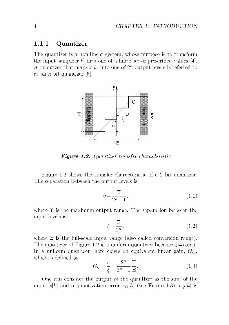
1.1.1 Quantizer
The quantizer is a non-linear system, whose purpose is to transform
the input sample x[k] into one of a finite set of prescribed values [4].A quantizer that maps x[k] into one of 2n output levels is referred to
as an n bit quantizer [5].
y*
Y
1)
Figure 1.2: Quantizer transfer characteristic
Figure 1.2 shows the transfer characteristic of a 2 bit quantizer.The separation between the output levels is
Tv-
1'i.r
where T is the maximum output range. The separation between the
input levels is
^2n
'1.2N
where S is the full-scale input range (also called conversion range).The quantizer of Figure 1.2 is a uniform quantizer because £ = const.
In a uniform quantizer there exists an equivalent linear gain, Gq,which is defined as
v 2n T
GQ = - =-^— A. (1.3)
One can consider the output of the quantizer as the sum of the
input x[k] and a quantization error eQ[k] (see Figure 1.3), eç)[k] is

1.1. A/D CONVERSION
Quantizer
Figure 1.3: Mathematical model of the quantizer
therefore the difference between y[k] and x[k],
eQ[k]=y[k]-x[k]. (1.4)
if x[k] is in the conversion range, then
\eQ[k]\<^ (1.5)
if x[k] is not in the conversion range, then
|eqW|>| (1.6)
and y[k] is said to be clipped.An important characteristic of a quantizer is its resolution, also
known as dynamic range (DR), defined as the ratio of a full scale
input sinusoid and the input referred quantization noise. Due to the
non-linear nature of the quantizer characteristic, and to the correla¬
tion of eQ[k] and x[k], it is difficult to make an exact analysis of the
quantizer. Nevertheless, it has been shown in [6] and [7] that with
some assumptions, the spectral density of eq[k] approaches that of an
additive, uniformly distributed white noise that is uncorrelated with
x[k\. The last sentence is referred to as the white noise approxima¬tion. The distribution peQ and the power spectral density Seq, of
ecf/c], under the white noise approximation are shown in Figure 1.4.
The power of a full scale sinusoidal x[k] and of the total inputreferred quantization noise are
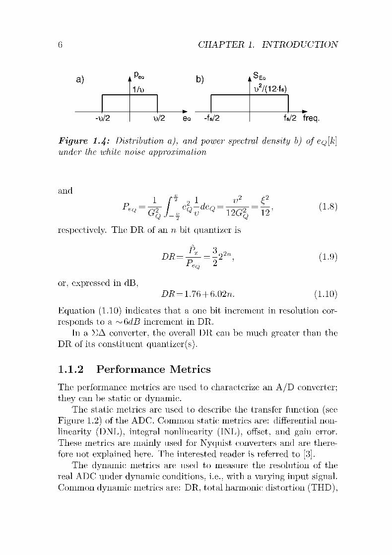
6 CHAPTER 1. INTRODUCTION
a).Pea
1/l)
-d/2 d/2 e(
b)
ea -fs/2
>Ea
0)7(12-fs)
fs/2 freq.
Figure 1.4: Distribution a), and power spectral density b) of eç)[k]under the white noise approximation
and
P.Q G
ïQ-dec^v
V
12Gi
respectively. The DR of an n bit quantizer is
DR=^ = -22n,P.
Q
or, expressed in dB,DÄ= 1.76 + 6.02n.
e12'
;i.9)
;i.io)
Equation (1.10) indicates that a one bit increment in resolution cor¬
responds to a ~6dB increment in DR.
In a EA converter, the overall DR can be much greater than the
DR of its constituent quantizer(s).
1.1.2 Performance Metrics
The performance metrics are used to characterize an A/D converter;
they can be static or dynamic.The static metrics are used to describe the transfer function (see
Figure 1.2) of the ADC. Common static metrics are: differential non-
linearity (DNL), integral nonlinearity (INL), offset, and gain error.
These metrics are mainly used for Nyquist converters and are there¬
fore not explained here. The interested reader is referred to [3].The dynamic metrics are used to measure the resolution of the
real ADC under dynamic conditions, i.e., with a varying input signal.Common dynamic metrics are: DR, total harmonic distortion (THD),

1.1. A/D CONVERSION 7
signal-to-noise ratio (SNR), and signal-to-noise-and-distortion ratio
(SNDR). These metrics are extensively used to characterize EA A/Dconverters. A list of the metrics with the corresponding explanationsfollows.
THD: Ratio between the sum of the power of the higher harmonics,and the power of the fundamental harmonic.
SNR: Ratio between the power of the fundamental harmonic, and
the power of the noise integrated on the band of interest.
SNDR: Ratio between the power of the fundamental harmonic, and
the sum of the power of the higher harmonics and of the noise,
integrated in the band of interest.
DR: Ratio between the power of the fundamental harmonic by full
scale input, and the noise floor integrated in the band of interest.
The dynamic performance metrics are usually given in dB.
In an ideal A/D converter, there is no distortion. Thus the THD
tend to be equal to minus infinity, the SNR and the SNDR are iden¬
tical, and the DR corresponds to the peak SNR and SNDR. In a real
A/D converter, the distortion usually degrades the resolution when
the input signal is near to full scale. Thus the THD, near full scale,is almost equal to the negative SNDR and the SNR is always largerthan the SNDR. Full scale input signals not only generate distortion
but also increase the noise floor, thus the DR is always larger than
the peak SNR. Finally, it must be observed that the dynamic metrics
depend also on the frequency of the input sinusoid.
In the design phase of EA converters, it is sometimes necessary
to consider thermal noise and quantization noise separately. For this
reason two supplementary performance metrics are introduced here,
namely, the signal-to-thermal-noise ratio (STNR) and the signal-to-
quantization-noise ratio (SQNR).
STNR: Ratio between the power of the fundamental harmonic, and
the power of the thermal noise integrated on the band of interest.
SQNR: Ratio between the power of the fundamental harmonic, and
the power of the quantization noise integrated on the band of
interest.

8 CHAPTER 1. INTRODUCTION
SNR, STNR and SQNR are linked by
SNR = 10logPthn + Pe
Q
= -101og(l0——+10-SQNR10 i.ir
where Pthn and PeQ are the thermal noise power and the quantizationnoise power, respectively.
1.2 Sigma-Delta A/D Converter
As stated in Section 1.1 the EA A/D converter is an oversampled con¬
verter. It consists of two blocks: the analog EA modulator that con-
x[k] y[k] yD[k]
lk_
XA
Modulator
Decimation
Filter
fB1
Figure 1.5: Block diagram of the EA converter
verts the analog input signal x[k] into an oversampled, low resolution,
digital signal y[k], and a digital decimation filter, that converts y[k]into a, high resolution, Nyquist rate, pulse-code-modulated (PCM),signal yD[k] (see Figure 1.5).
The first time that a similar architecture has been published was
in 1969 [8]. The main difference, with the current architecture, was
that instead of employing a EA modulator, it used a simple delta
modulator. The first converter employing a EA modulator was pub¬lished five years later [9], although the AE1 modulation was alreadyknown for 12 years [10].
1The name of the modulation in the first paper was AE modulation. The A
before the E probably meant that the difference operation A, is placed in front

1.2. SIGMA-DELTA A/D CONVERTER 9
In these early days, the main obstacle to the broadening of the
technique, were the high implementation costs of the digital circuits
required in the decimation filter [11]. Nowadays, the situation has
completely changed. Modern computer-aided design (CAD) tools
have made the generation of digital circuits almost automatic, and
the power consumption of digital devices has been strongly reduced.
In contrast to this, the complexity of the analog circuit design has re¬
mained almost unchanged. Thus the main obstacle to the broadeningof EA converters in their early days has become the main engine of
their success, today.
1.2.1 Sigma-Delta Modulator
x[k] xn[k]Loopfilter
Quantizer
yA[k]
Figure 1.6: Block diagram of the EA modulator
The block diagram that is usually taken to describe the opera¬
tion of a EA modulator is illustrated in Figure 1.6. The analog low-
pass input sequence x(k) is oversampled; H(z) represents an analogdiscrete-time filter, also called loopfilter; the quantizer generates a dig¬ital sequence y[k] that is the sum of yh[k], the output of the loopfilter,and ecf/c], the quantization error.
The discrete-time filter shown in Figure 1.6 is very difficult to
analyze in its full generality, due to the nonlinear quantizer. It only
appears possible to arrive at useful results, when assumptions are
made concerning x[k] and H(z) [12] - [15], or when the quantizer linear
model is taken (see Section 1.1.1). This second method, combined
of the integrator E. The first authors of converters, based on the AE modula¬
tion called their circuits EA converters, to point out that they used a delta (A)modulator preceded by an integration operation E. In this book we use EABoth
nomenclatures, EA and AE refer exactly to the same method.

10 CHAPTER 1. INTRODUCTION
with the extensive use of numerical simulations, is sometimes the only
existing method for the design of high-order modulators.
Next linearization of the quantizer will be considered to explain the
operation of the modulator. Denoting the z-transforms of the input,
noise and output sequences by X{z), Eq{z) and Y{z), respectively,it can be concluded that the signal transfer function (STF) and the
noise transfer function (NTF) are
STF{z)
NTF(z)
Y(z)
X(z)
Y(z)Eo(z,
H(z)
Eq(z)=0
X(z)=0
1 + HizY
1
1 + H(z)
'I.I2:
;i.i3)
If the loopfilter is chosen to have a large gain over the signal band
fß and a gain much lower than the one outside, the gain of the STF
is close to one in fß and close to zero outside. On the other hand,the gain of the NTF is close to zero in fß and close to one outside.
Therefore the spectrum of y [k] is approximately equal to the spectrum
of x[k] in fß, and contains noise outside. This redistribution of the
quantization noise towards high frequencies is referred to as noise
shaping. Noise shaping is advantageous because the spectrum of x[k]can be recovered quite accurately by lowpass filtering.
xn[k] Delay
<> D
yh[k]
Figure 1.7: Discrete time integrator
The simplest operator that fulfills the above mentioned require¬
ments for H{z) is the integrator. Figure 1.7 shows a discrete-time
integrator. A EA modulator with a simple integrator is referred to
as first order modulator because of the order of H{z). The steepness
of the NTF in the transition from almost zero to one, gives the shap¬
ing capability of the modulator. The steepness can be increased by
increasing the order of H(z). The order cannot be freely increased

1.2. SIGMA-DELTA A/D CONVERTER 11
because the higher the order, the less stable the modulator becomes.
Depending on the OSR and on the number of bit n in the quantizer,
there is an order, after which, the reduction of the quantization noise
power, in fß, is compensated by the reduction of the maximum stable
input amplitude. This order is lower for modulators with a low OSR
and a small n.
The stability problem arises when the order of H(z) is higher than
two. The linear model cannot predict if a designed H(z) will turn
into a stable modulator, or not. In the linear model, the quantizer is
substituted by a constant gain Gq, while the instant gain
°«[fcl=ä- (L14)
in a real quantizer is variable. Thus one can not predict if the polesof the real system will be inside the unit circle (stability criterion),or not. Since the higher is n, the less variâtes Gq[/c], the accuracy of
the linear model increases with the number of bits in the quantizer.
However, the only secure way to proof a modulator for stability is by
computer simulation.
The design of a EA modulator consists in the optimal choice of
OSR, n, and H(z), and in the optimal realization of H(z). There is no
simple solution to this problem, since the optimal choice depends on
many parameters such as, the required resolution, the bandwidth, and
the power consumption. The existing architectures of EA modulators
will be introduced in Chapter 2 and will be analyzed with regard to
the goal of this thesis.
Before concluding this section an important hidden problem should
be pointed out. In Figure 1.6 a digital-to-analog (D/A) converter
in the feedback path has been neglected. Indeed, the y[k] must be
converted into an analog signal yA[k] before being subtracted to x[k\.As it will be shown in Chapter 3, if the D/A converter is not perfectly
linear, the DR of the modulator is strongly degraded. EA modulators
with single bit quantizer do not suffer from this problem, since theyhave a two level D/A converter. The two level D/A converter is
intrinsically linear because it is always possible to draw a straight line
that connects two points. Unfortunately, the singlebit quantizer has a
poor DR (see Section 1.1.1) and is not suited for EA converters with
a low OSR.
12 CHAPTER 1. INTRODUCTION
For the sake of completeness it must be mentioned that H(z) can
have both, a lowpass and a bandpass characteristic. In the latter
case the input signal is sampled at four, to eight, times the central
frequency loq, and the noise is minimized only around its band. The
output y[k] is then decimated and mixed to baseband in the digitaldomain. In the context of a communication system, early conversion
to digital at either the intermediate or radio frequency stage results in
a more robust system with improved intermediate-frequency (IF) strip
testability and provides opportunities for dealing with the multitude
of standards present in commercial broadcasting and telecommunica¬
tions [16]. In particular, the IF filter can be pushed to the digital
domain, where testing is systematic and changing filter coefficients is
easy.
This thesis considers only the lowpass EA converter. For bandpassEA converters, the reader is referred to the literature [16].
1.2.2 Decimation Filter
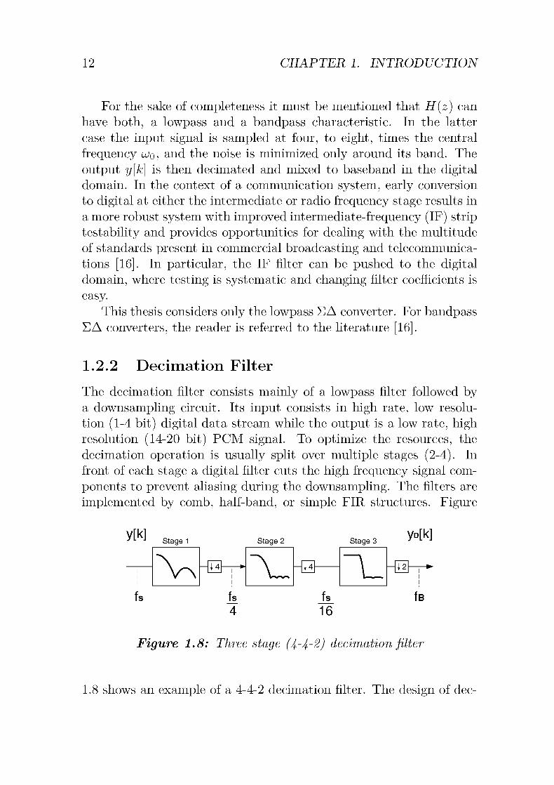
The decimation filter consists mainly of a lowpass filter followed bya downsampling circuit. Its input consists in high rate, low resolu¬
tion (1-4 bit) digital data stream while the output is a low rate, highresolution (14-20 bit) PCM signal. To optimize the resources, the
decimation operation is usually split over multiple stages (2-4). In
front of each stage a digital filter cuts the high frequency signal com¬
ponents to prevent aliasing during the downsampling. The filters are
implemented by comb, half-band, or simple FIR structures. Figure
Stage 1 Stage 2
A k A_14,
1-
Stage 3
A 1_i4
yD[k]
12
k4 16
fB
Figure 1.8: Three stage (4~4-2) decimation filter
1.8 shows an example of a 4-4-2 decimation filter. The design of dec-

1.3. DESIGN CHALLENGES 13
imators is not the central topic of this thesis, the interested reader is
referred to [16].
1.3 Design Challenges
Modern deep sub micron digital technologies, allow fast devices and
very dense system integration, while keeping the power density con¬
stant. Indeed the interconnections capacitors are reduced and the
supply voltage decreased. Along with the appreciated increment in
speed, from the point of view of the analog designer, this scaling trend
brings many disadvantages: the low voltage supply and the increment
of the device intrinsic noise reduces the DR of the on-chip signals, the
short channel length reduce the voltage gain of the devices.
Nevertheless it is economically very attractive to take the same
main stream technology for both, the A/D interface and the digi¬tal circuitry, not only because both parts can be integrated onto the
same chip, but also because the same voltage supply can be used, and
because no special interfacing circuitry is required; and also because
main stream technologies are cheaper and more dense than analog ori¬
ented technologies, and also because reducing the number of different
technologies used for a product reduces the administrative costs.
In monolithic realizations, EA A/D converters are preferred to
Nyquist A/D converters because of their simplicity. Indeed, they do
not need a sample-and-hold (S/H) circuit, and they put relaxed re¬
quirements on the anti-aliasing filter. With respect to the Nyquist
A/D converters, that suffer from the DR reduction, EA converter
can also efficiently trade off speed for resolution. Since they do not
require circuit calibration or device trimming to achieve more than
12 bit of resolution, they are very well suited for implementations, in
deep sub micron technologies, that require high resolution A/D con¬
verters. However, in spite of the fast devices, EA modulators still
suffer from lack of speed, since higher OSRs are needed to cope with
the lower DR.
To be compatible with the majority of the modern digital sig¬nal processing applications (mainly communications applications), the
A/D converter does not only have to provide high resolution, but also
high conversion rates. Thus, the primary goal of this work is to re-

14 CHAPTER 1. INTRODUCTION
search converter architectures which are able to provide high reso¬
lution at low OSR. However, this condition alone does not ensure a
high conversion rate unless the sampling speed is also maximized. The
choice of the architecture has to take care also of this second aspect,
that has been very often omitted in similar studies [42].
1.4 Organization of the Thesis
This thesis discusses the development and the design of two broadband
EA modulators for ADSL and VDSL communications applications,
respectively. The structure of the thesis follows the development from
the choice of the basic architecture to the implementation of the analog
building blocks composing the final modulators.
Chapter 2 describes the existing architectures used to implementEA modulators. The possible implementations are sorted into eightclasses and are analyzed comparing complementary solutions. The
goal is to find the architecture that is best suited for the implementa¬tion of broadband EA modulators. The main motivation underlyingthe whole Chapter is that the best final performance is reached onlywhen the architecture that puts the most relaxed specifications on the
building blocks is selected.
One of the conclusions drawn in Chapter 2 is the need of a multibit
quantizer. Since a multibit quantizer implies a DAC with more than
two output levels, the linearity of the DAC becomes a very critical
parameter of the design. Chapter 3 describes an attempt to find an
analytical solution for the estimation of the performance degradationdue to the DAC nonlinearity. The assumptions taken to simplify the
modulator model are firstly explained. Then the final equation is
given and is exactly solved for the case of a 5th order trilevel DAC
EA modulator. Simulated and calculated results are finally comparedand discussed.
Chapter 4 explains the first design of this thesis which consists
of a EA modulator for ADSL standard with 14 bit of resolution and
2.5 MS/s. The design is approached in a top-down fashion: startingfrom the architecture level, where the parameters remained undefined
from Chapter 2, are given; continuing with the switch level, where
the SC implementation is explained; and ending in the circuit level,

1.4. ORGANIZATION OF THE THESIS 15
where the specifications and the implementation of the analog buildingblocks is shown. The Chapter closes with the presentation of the
experimental results.
The good measurement results of the ADSL EA modulator allow
us to go one step further in the development, namely to increase the
conversion speed. In Chapter 5, the implementation of a VDSL EA
modulator with 25 MS/s and 14 bit resolution is described in detail.
The design is also approached in a top-down fashion and closes with
the presentation of the experimental results, as well.
Chapter 6 begins with a summary of the thesis for the hurried
reader. This summary also serves as the basis for the concludingcomments on the results achieved in this thesis and for the discussion
on the issues not covered by this work that would be interesting to be
further investigated.


Chapter 2
Architectures
The performance of a EA modulator is mainly determined by the
performance of the analog building blocks whose specifications are
dictated by the selected architecture. Therefore it is of particular
importance to choose the best possible architecture that relaxes the
specifications on the analog building blocks to enable the final perfor¬mance to be more easily achieved. For this reason an entire chapterof this work is dedicated to the discussion of the EA architectures.
There are so many different ways to implement a EA modulator
that an exhaustive review would take many pages. Nevertheless, EA
architectures can easily be sorted in eight different classes. Namely,discrete-time (DT), continuous-time (CT), cascaded, single-loop, sin-
glebit, multibit, feedforward (FF), and feedback (FB).This chapter is organized in five sections. Each of the first four
sections will present, two of the eight above mentioned classes. To
simplify the discussion two complementary classes will be taken. At
the beginning of each section the basic architectural differences will
be mentioned. The second part will instead go into more details on
studying how these differences translate into the actual modulator im¬
plementation, from a theoretical and a practical point of view. This
includes the study of several aspects such as the stability of the loop,the shaping capability, the sensitivity to circuit and signal nonideal-
ities, the circuit complexity, and the power consumption. The final
part will point out the main motivation of why an architecture is
17

18 CHAPTER 2. ARCHITECTURES
better suited for the implementation of broadband EA modulators.
The fifth section will then recapitulate the main conclusions of
the previous sections and will provide the guidelines for the following
designs.
2.1 Continuous-Time vs. Discrete-Time
There are three attributes that differentiate a CT from a DT archi¬
tecture; namely, the position of the sampler, the type of the loopfilter,and the operation of the feedback DAC. The following sections will
point out the consequences of each of these differences on the benefits
of one architecture class in respect of the other.
2.1.1 Sampler Position
The position of the sampler is a basic difference between the CT and
the DT architecture. As shown in Figure 2.1, in the CT architecture
a; Loopfilterm
(Quantizer
X(t) Xh(t)
H(s)yn(t)
f'
y[k]
yA(t)nAPUrtU
b)
x(t).y
Loopfilter Quantizer
fs
yA[t]
Xh(t)
H(z)yh(t) y[kj
I
rapUAU
Figure 2.1: Block Diagram of a continuous-time (a) and of a
discrete-time (b) EA modulator.

2.1. CONTINUOUS-TIME VS. DISCRETE-TIME 19
the signal is sampled at the quantizer1, i.e., at the loopfilter back-end
while in the DT architecture the signal is sampled at the input of the
modulator, i.e., at the loopfilter front-end.
The sampling operation is always linked with the uncertainty of
the sampling instant caused by the clock jitter. In the literature, the
clock jitter is usually modeled as a white, normal distributed, mean
free, clock period variation Ar[k] with standard deviation <jat- The
influence of the clock jitter on the sampling operation is calculated
first.
If a sinusoidal signal x(t) = A sm(27rft) is sampled at time intervals
defined by a noisy clock the sampling error at time kTs is given by
ej[k]=Asm(27rf(kTs + Ar[k]))-Asm(27rfkTs) (2.1)
i.e., by the difference between the signal sampled at noisy time in¬
tervals Ts + Ar[/c] and the signal sampled at clean time intervals Ts.
Since 2tt/At[A;]<1,
ej[k] ^27rfAT[k]Acos(27rfkTs). (2.2)
The variance of ej [k]
N
J=n^oo2NTÏ è (27r/Ar[/cMcos(27r//cTs))2 (2.3)k=-N
gives then the power of the error due to the non-zero Ar[fc], By
assuming that Ar[k] and xW\ = cos(2ttfkTs) are signals generated bytwo ergodic processes, Equation (2.3) can be rewritten as
-I /OOpi
/ AtVp(At,xMx,At) (2.4)-ooJ-l
where p(Ar,x) is the two-dimensional probability distribution func¬
tion of Ar and x- However, since Ar and x are statistically indepen¬
dent,
p{At,x)=p{At)p{x) (2.5)
1The idea of sampling at the quantizer and using a CT loopfilter in a EA
modulator dates to 1984 when, in [19], a EA A/D converter for digital audio
application employing a passive, second order, loopfilter has been published. The
circuit was fabricated using a 3.5 um CMOS technology, and achieved 13 bit over
20 kHz with 256 OSR.

20 CHAPTER 2. ARCHITECTURES
Equation (2.3) can be rewritten as
/OOpi
Ar2p{Ar)dAr- x2p(x)dX (2.6)-oo J — 1
where the two integrals represent the individual contributions of Ar
and x to the error power, respectively. Since
/oo Ar2p{Ar)dAr = a'iT (2.7)-oo
and
f1 1
J xMx)dX=^ (2.8)
the variance can be expressed as:
o2ej=^2f2A2o\T. (2.9)
Equation (2.9) shows that, given a fixed noisy clock source with stan¬
dard deviation <7at, the error power caused by the clock jitter is pro¬
portional to the square of both the amplitude and of the frequency of
the signal to be sampled.
The position of the sampler at the loopfilter back-end can be con¬
sidered an advantage of the CT with respect to DT architecture. On
one hand, in the DT architecture the sampling error gets multiplied
by the STF thus, its power in fß appears unchanged at the output.
On the other hand, in the CT architecture the sampling error gets
multiplied by the NTF therefore its power in fß is highly attenuated.
However, it must also be noted that since the maximum frequencyat the sampler in the DT architecture is fß while the maximum fre¬
quency at the sampler in the CT architecture is fs/2 (y^ contains
quantization noise at high frequencies) the power of the sampling er¬
ror in the CT architecture is higher. Nevertheless this is not a real
problem for CT architectures, since the increment of the noise power
is usually much less than the attenuation of the NTF.
An other advantage of the CT architecture is that since the sam¬
pler is at the loopfilter back-end the aliasing components are also

2.1. CONTINUOUS-TIME VS. DISCRETE-TIME 21
multiplied by the NTF and are thus also strongly attenuated2. Fur¬
thermore, the loopfilter in CT architectures isolates the sampler from
the input node avoiding the generation of kickback noise. These are
all benefits that the DT architectures do not have. However, the po¬
sition of the sampler is not the only difference between the CT and
the DT architecture.
2.1.2 Loopfilter Type
Figure 2.1 shows that the CT architecture has a CT loopfilter H(s)while the DT architecture has a DT loopfilter H(z)
Due to this, more aggressive noise shaping can be achieved by DT
with respect to CT loopfilters. In fact, DT loopfilters are implemented
using the SC technique, thus employing very precise coefficients (ca¬pacitor ratios). Furthermore, analog/digital filter matching can be
easily obtained since DT analog and digital filters are of the same
type (discrete-time). Finally, time isolation can be used in DT filters
at circuit level to reduce coupling of digital noise (e.g., from the deci¬
mation filter) into the analog path since internal signals must be clean
only at the instant when the sampling switches are opened.
Since the loopfilters of the two architecture classes have quite dis¬
tinct working principles, they should also put different specifications
on their active analog building blocks. Thus, it would be interesting to
know which of the two filter types dictates the lowest specifications at
comparable modulator performance. This is not a simple task, since
on the one hand CT filters have slower transients, but they must be
very precise (linearity). On the other hand DT filters have faster tran¬
sients but need only be precise at the end of the sampling interval.
Furthermore, slewing is allowed in amplifiers used in DT filters while
this is strictly forbidden in CT filters. This problem has not been
solved during this work. Nevertheless, it could be a interesting issue
for further investigations.
2It has been shown in [17] that, under the assumption that the hold function in
the feedback path has a lowpass characteristic, with notches at m- fs, the aliasing
component of an input signal with frequency fs — fß is reduced by p(fs — fß) =
TT/r_r x.H(f) decreases by approximately L-20 dB/dec.

22 CHAPTER 2. ARCHITECTURES
2.1.3 DAC Operation
There is an other basic difference between the CT and the DT archi¬
tecture that is not as explicit as the previous two, but unfortunately is
by far the most important. In the EA modulator, a DAC in the feed¬
back path is required to convert the digital signal y[k] into an analog
signal ya (see Figure 2.1). Since x(t) is sampled before entering the
input node, ya is a DT signal in the DT architecture. In contrast to
this, ya is a CT signal in the CT architecture, as here the samplingtakes place at the back-end of the loopfilter. Thus, the feedback DAC
in a CT architecture not only has to convert a discrete-time digital
signal into a discrete-time analog signal but the signal must also be
continuous-time. This extra task produces two additional sources of
error. Since these errors take place at the modulator input node,which is the most sensitive node, the CT architecture turns out on
putting overall higher specifications on the analog building blocks,than its DT counterpart.
The unavoidable delay in the feedback path reduces the stabilityof the loop and the shaping capability of the modulator. Indeed, some
time is required from when the signal is sampled to the moment it is
digitally converted, analog re-converted, and fed back to the input.Since the input is CT, at the time the output is fed back to the input,
the input signal has already changed, compared to its value at the
time the sampling operation has taken place. Furthermore, one has
to take care that the loop delay is not signal dependent, otherwise a
supplementary error is introduced. (The problem of the excess loop
delay has been studied in depth in [18].)In the CT architecture the summation operation is carried out by
currents. The second source of error is the variation of the duration
of the DAC feedback current pulses. Since in usual CT implementa¬tions the duration of the current pulses is defined by the clock signal,the clock jitter Ar defines a small random variation in the chargetransfered during a clock period.
Figure 2.2 shows a simplified CT integrator combining input pathand 1-bit feedback DAC. The behavior of its internal currents ix(t)and iDAc{t) are also illustrated. The DAC is of return-to-zero (RZ)type and generates current pulses with amplitude IdAC and rate fs =
1/TS. The input signal ix(t) is the dashed curve, it is a sinusoid with
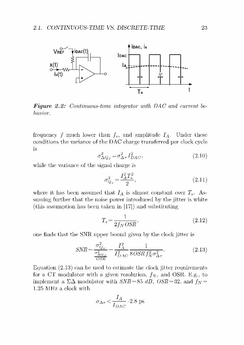
2.1. CONTINUOUS-TIME VS. DISCRETE-TIME 23
VREF ^ÎDAc(t)
x(t)o—^-Wv
ix(t)
n ÎDAC, ix
I DAC
Ia
At
Ts
Figure 2.2: Continuous-time integrator with DAC and current be¬
havior.
frequency / much lower than /s, and amplitude I
a- Under these
conditions the variance of the DAC charge transferred per clock cycleis
<taqj=<tAtIdac, (2-10)
while the variance of the signal charge is
OrI\T2
:2.ir
where it has been assumed that I
a is almost constant over Ts. As¬
suming further that the noise power introduced by the jitter is white
(this assumption has been taken in [17]) and substituting
1
s
2fNOSR
one finds that the SNR upper bound given by the clock jitter is
,2 t2
:2.i2:
SNR--Or I
A
1
TU.j ItjAC80SRf^ai12.13)
OSR
Equation (2.13) can be used to estimate the clock jitter requirements
for a CT modulator with a given resolution, /jv, and OSR. E.g., to
implement a EA modulator with SNR = 85 dB, OSR = 32, and /jv =
1.25 MHz a clock with
0"At<
I
A
IDAC
2.8 ps

24 CHAPTER 2. ARCHITECTURES
is needed. This requirement is quite hard to obtain and is even wors¬
ened by the fact that, the loop stability requirements are involved and
since the duty cycle of the DAC is usually less than one, -p"*— <C 1.
In DT EA modulators implemented using the SC technique the
current pulses generated by the DAC have the shape of an exponential
curve settling to zero. The error in charge transfer due to the random
variation of the DAC pulse duration is thus much smaller.
The sensitivity of CT architectures to the variation of the dura¬
tion of the DAC feedback current pulses is the main reason why DT
architectures are better suited than CT architectures for the imple¬mentation of broadband modulators.
2.2 Cascaded vs. Single-Loop
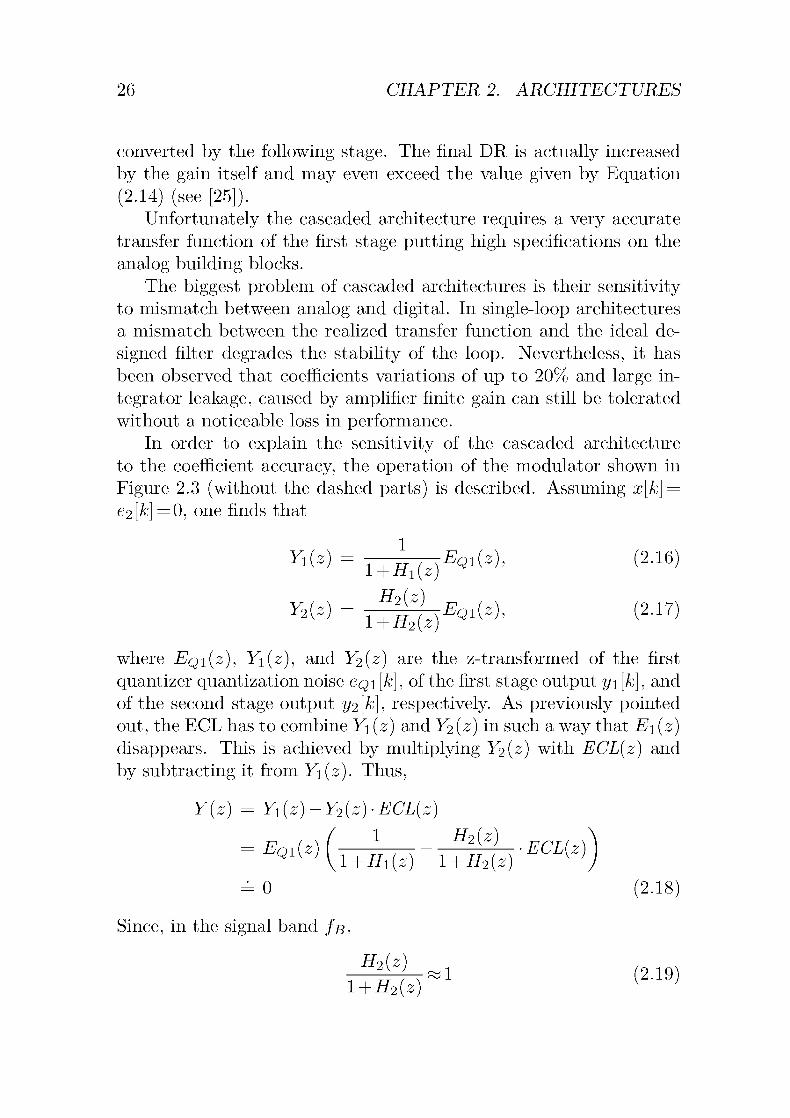
In this section the cascaded and the single-loop architecture will be
compared.
The main difference between the cascaded3 and the single-loop ar¬
chitecture is the number of conversion stages. The single-loop archi¬
tecture has only one conversion stage, while the cascaded architecture
has more conversion stages. In most of the published implementationsthe stages are all made by EA modulators, but this is not mandatoryas has been shown in [20] and [21]. This section will only consider the
"full-EA " cascaded architectures.
Figure 2.3 shows a block diagram of a possible implementation;several single-loop modulators can be seen, where each stage takes the
error of the previous quantizer and digitizes it. The output streams
are then combined in the error correction logic (ECL) in such a way
that each quantization error ecj/c], but the one generated in the last
stage, is cancelled. The result of this exercise is that, if every operation
is exact, the remaining noise is shaped with an order equal to the sum
of the orders of the employed loopfilters.
3This technique was proposed for the first time with two cascaded delta mod¬
ulators, in 1967 [22], and it has been applied to the EA modulation only 20 years
later [23]. The authors of [23] named the cascaded architecture, the MASH ar¬
chitecture. Unfortunately they did not provide any explanation for the name.
Nevertheless, the cascaded modulators are often also called MASH modulators.
Both names stay exactly for the same method.

2.2. CASCADED VS. SINGLE-LOOP 25
x[k] „_
Loopfilter 1
Hi(z)
<±>
Loopfilter 2
H2(z)
_u
<±>
7-<
yi[k]
ECLy[k]
y2[k]
Figure 2.3: Cascaded EA modulator.
In [24], it has been shown that OSR, n and L of iï"(^) are related
to the dynamic range of the EA modulator by
DR=—(2n-
2v ir(2L+r
fOSR\2L+1I2-14)
where the white noise approximation is used and
NTF(z) = (l-z~1)i\L
:2A5)
is assumed. Equation (2.14) is exact for L<2. However, as pointedout in Section 1.2.1, stability considerations prevent the NTF shown
in Equation (2.15) from being implemented when L>2. As a result,the effective DR in L > 2 single-loop modulators is usually lower than
that predicted by Equation (2.14). Cascaded modulators, instead,do not need loops with L>2 to achieve higher order noise shaping.
Hence, they have better stability and they usually reach higher DRs
at similar OSR, n, and L conditions.
In addition, the architectures with cascaded loops also take also
advantage of the fact that the quantization noise is reduced when
the residual error of an internal quantizer is amplified, before being
26 CHAPTER 2. ARCHITECTURES
converted by the following stage. The final DR is actually increased
by the gain itself and may even exceed the value given by Equation
(2.14) (see [25]).Unfortunately the cascaded architecture requires a very accurate
transfer function of the first stage putting high specifications on the
analog building blocks.
The biggest problem of cascaded architectures is their sensitivityto mismatch between analog and digital. In single-loop architectures
a mismatch between the realized transfer function and the ideal de¬
signed filter degrades the stability of the loop. Nevertheless, it has
been observed that coefficients variations of up to 20% and large in¬
tegrator leakage, caused by amplifier finite gain can still be tolerated
without a noticeable loss in performance.In order to explain the sensitivity of the cascaded architecture
to the coefficient accuracy, the operation of the modulator shown in
Figure 2.3 (without the dashed parts) is described. Assuming x[k] =
e2[k] =0, one finds that
Y^z) = Tïk(z)EQl{z)' (2'16)
Y^ = iä&^w- (2-17)
where Eq\{z), Y\{z), and 12(2) are the z-transformed of the first
quantizer quantization noise eQi[/c], of the first stage output yi[k], and
of the second stage output 2/2^], respectively. As previously pointed
out, the ECL has to combine Y\{z) and 12(2) in such a way that E\{z)disappears. This is achieved by multiplying 12(2) with ECL(z) and
by subtracting it from Y\{z). Thus,
Y(z) = Y1(z)-Y2(z)-ECL(z)
^«(ïTÏÏW-ïaËw^H= 0 (2.18)
Since, in the signal band /#,
H2(z)_
1 + H2(z]r^j [2.19)

2.2. CASCADED VS. SINGLE-LOOP 27
Equation (2.18) is satisfied when
ECL(z]1 + HUz)
;2.20)
which means that ECL(z) has to be equal to Y\{z). Indeed, if there is
a mismatch between ECL(z) and Y\{z), Equation (2.18) is not zero,
and part of the noise of the first quantizer leaks into Y{z).To get an idea of how good the matching between the digital and
the analog transfer function should be, an example is given. From
Equation (2.18) it is known that the quantization noise of the first
quantizer Eq1(z) that leaks into Y{z) is
Yleakage(z)nEQl (nTF^z) ~ NTF^z] :2.2r
where NTFl(z) and NTF1(z) are the analog and the digital imple¬mentation of the first stage NTF, respectively. To provide intrinsic
stability the order of NTF\{z) has to be less than two.
xi[k]
-^-i 1-z1
eoi[k], yi[k]
Figure 2.4'- Possible realization of a second order HA modulator foran input stage of a cascaded architecture.
A possible implementation of a NTF\{z) with order two is shown
in Figure 2.4. The ideal NTF of the depicted modulator is
NTF(=(l-z~1)2,
while the NTF assuming integrators with transfer function
(l-a^z-1Hz.
l-{l-ß)z~1
'2.22'
'2.23'

28 CHAPTER 2. ARCHITECTURES
where a and ß are the gain and the pole error, is
NTFl = -, r-,r4i
w. V-^-
(2.24)1
-1 1 (l-ai)(l-a2)z2
I 2(l-a2)z 1 v '
1+(l-(l-ßl)z-i)(l-(l-ß2)z-i)
"t-i_(i_Ä)z-i
where ai, ß\, a2l and /?2 are the gain and the pole error of the first and
the second integrator, respectively. By substituting Equation (2.22)and Equation (2.24) in Equation (2.21) and by solving the resulting
expression assuming that a.\, ß\, a2l ß2 «Cl and that \z — l|<Cl one
finds
Yieakage{z)^EQl{z) 'i-d-JihA,-! (A+A). (2.2.5;
Hence, Yieakage{z) is the first-order shaped Eq1(z) attenuated by the
factor ß\-\-ß2- The DR of a first order modulator has been givenin Equation (2.14) for L = l; by adding the effect of the attenuation
factor ßi + /?2 one finds that
DRleakage = mog(^{2n-l)OSRi}-20log{ß1+ß2). [dB]
(2.26)The contribution of the leaked noise should obviously be negligible
compared to any other noise contribution. The quantizer number of
bits n and the OSR are characteristics of the architecture while ß
depends on the actual implementation of the analog integrator. The
link between the ß factor and the SC integrator, implemented byan operational transimpedance amplifier (OTA) with transimpedance
Gmi output impedance Ro, feedback capacitance Cp and sampling
capacitance Cs, has been given in [43], and is
201og(/?)«-201og i1^0^) (2.27)
Hence, ß mainly depends on the closed-loop gain of the OTA.
The case of a modulator with OSR= 32, a first stage with order
two, a single-bit quantizer, DR= 86 dB (14 bit), and a leakage noise
20 dB below the noise floor is presented as an example. By substitut¬
ing the given data in Equation (2.26) one finds
201og(/?i+/?2) = 42 dB-106 dB = -64 dB. (2.28)

2.3. MULTIBIT VS. SINGLEBIT 29
Assuming further that ßi=ß2 = ßi (2.28) demands that 201og/? =
—70 dB. Since the two paths present at the input of each integra¬tor of the first stage shown in Figure 2.4 are usually implemented by
separate capacitors, Csi/Cpi = 2 and Cs2/Cp2 = 3. By substitution
of all known data in Equation (2.26) one finds that the open-loop gain
requirement for the used OTAs are
201og(Gmi/GOi) = 201og3 + 70 dB = 80 dB (2.29)
and
201og(Gm2/GO2) = 201og4 + 70 dB = 82 dB, (2.30)
respectively. These requirements are not hard to achieve if the OTAs
are implemented by moderate sub-micron integration technologies.
However, they become critical when fast deep sub-micron technologiesare selected.
Since high fs is required in broadband EA modulators, fast deepsub-micron are welcomed for their implementation. Hence, it is prefer¬able to choose an architecture that is insensitive to the OTA open-loop
gain. As a consequence the single-loop architecture is more suited
than the cascaded architecture for the implementation of broadband
modulators.
2.3 Multibit vs. Singlebit
The main difference between the multibit and the singlebit architec¬
ture is that the singlebit architecture has a quantizer with n = 1 while
the multibit architecture has a quantizer with n>l. This has several
consequences on the main benefits of the two architecture classes.
The main quality of EA modulators employing multibit quantizersis that the ratio of the total quantization noise power to the signal
power at the modulator's output is dramatically reduced, comparedto that of a modulator with singlebit quantizer, typically by 6 dB
per additional bit. Therefore, it is possible to increase the overall
resolution of any EA A/D converter, without increasing the OSR,
simply by increasing the number of levels in the internal quantizers.
Equivalently, the architectures with multibit quantizers can achieve
resolutions comparable to that of architectures with singlebit quan¬
tizers at lower OSR.

30 CHAPTER 2. ARCHITECTURES
Architectures with a L > 2 loopfilter can also benefit from the more
stable instantaneous gain G[k] (see Section 1.2.1) of the quantizer,
because the better the gain of the quantizer is known, the more stable
is the loop and the more aggressive can be the noise shaping. As a
result, higher DRs can be obtained at the same OSR. In Chapter 4 it
will be shown that using a 1.5 bit quantizer instead of a 1 bit quantizer,in a bth order EA modulator, with a single loop, may increase the final
DR by 10 dB. This happens despite the fact that the DR of a 1.5 bit
quantizer is only 6 dB higher than that of a 1 bit quantizer.Architectures with cascaded loops can also benefit from the use of
multibit quantizers. In Section 2.2 it has been stated that the DR can
be increased, by introducing a gain factor between two stages. If a
singlebit quantizer is employed, the generated quantization noise is so
large that an attenuation factor is required, to prevent the next stage
from saturating. This translates into a loss of DR. With a multibit
quantizer, on the other hand, the generated quantization noise is much
smaller and a gain factor larger than one can be used. As a result,the final DR is increased not only by 6 dB per added bit, but also
by the gain factor of the introduced stage. Furthermore, since the
quantization noise becomes "more random" as the number of bits in
the quantizer is increased, the tone performance of the single loopswith L < 2 is improved.
The main quality of architectures employing a singlebit quantizer
is the simplicity of the circuit implementation of the quantizer. In a
single bit quantizer only a single comparator is required. Any offset in
the comparator is handled as a constant DC term, added at the output
of the modulator and is therefore multiplied with the NTF. Since the
NTF has zeros at DC, the offset of the comparator is completely can¬
celed. Not only the quantizer is simple in a singlebit architecture but
also the circuit that provides the signal to the quantizer (e.g., the last
integrator in a feedback architecture or the weighted summing circuit
in a feedforward architecture). Furthermore, since the singlebit quan¬
tization is very coarse the accuracy required at the circuit precedingit is very low.
Another property of the singlebit architecture is that the accuracy
of the feedback DAC does not determine the linearity of the inputnode. The output of the DAC is subtracted from the input signal at
the input node. Since the input node has to meet the linearity spec-
2.3. MULTIBIT VS. SINGLEBIT 31
ification of the entire modulator, the DAC must fulfill the linearity
specification, as well. However, with two levels it is impossible to gen¬
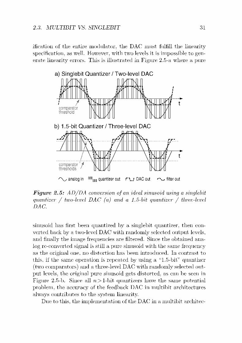
erate linearity errors. This is illustrated in Figure 2.5-a where a pure
a) Singlebit Quantizer/Two-level DAC
^\y analog in mm quantizer out r\j DAC out 'N, filter out
Figure 2.5: AD/DA conversion of an ideal sinusoid using a singlebit
quantizer / two-level DAC (a) and a 1.5-bit quantizer / three-level
DAC.
sinusoid has first been quantized by a singlebit quantizer, then con¬
verted back by a two-level DAC with randomly selected output levels,and finally the image frequencies are filtered. Since the obtained ana¬
log re-converted signal is still a pure sinusoid with the same frequencyas the original one, no distortion has been introduced. In contrast to
this, if the same operation is repeated by using a "1.5-bit" quantizer
(two comparators) and a three-level DAC with randomly selected out¬
put levels, the original pure sinusoid gets distorted, as can be seen in
Figure 2.5-b. Since all n> 1-bit quantizers have the same potential
problem, the accuracy of the feedback DAC in multibit architectures
always contributes to the system linearity.Due to this, the implementation of the DAC in a multibit architec-

32 CHAPTER 2. ARCHITECTURES
ture is very critical. However, as already pointed out, the large amount
of quantization noise generated by the singlebit quantizer limits the
noise shaping capability of the modulator at low OSRs. Hence, for the
implementation of broadband EA modulators the choice of a multibit
architecture is usually mandatory. For this reason, some techniquesto cope with the nonlinearity of the feedback DAC will be presentedin the coming sections.
2.3.1 Laser Trimming
A first post processing linearization technique makes use of laser trim¬
ming. Trimming of capacitors is typically done by switching off very
small capacitors parallel to the capacitor being trimmed. This tech¬
nique requires little effort from the point of view of the circuit design,as one can assume that the DAC is ideally linear. Thus, trimmed
multibit DACs are as simple as untrimmed DACs. Unfortunately, the
trimming operation requires a big effort in the preparation of the chip.Laser trimmed chips are very expensive and require special infrastruc¬
tures to be produced.
Furthermore, variations in matching with temperature, power sup¬
ply voltage, age, and so on cannot be compensated by this method;
performance can drift during operation.
2.3.2 Digital Correction
A second post processing linearization technique uses digital correc¬
tion.
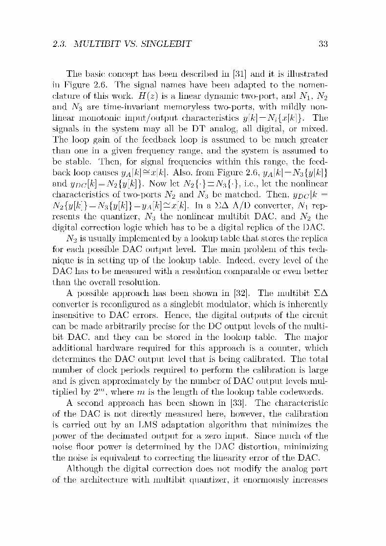
<[V - H(z) Ni
Ns
y[k]N2
y°
1 V
fA[k]
Figure 2.6: General block diagram of the digitally corrected system.
2.3. MULTIBIT VS. SINGLEBIT 33
The basic concept has been described in [31] and it is illustrated
in Figure 2.6. The signal names have been adapted to the nomen¬
clature of this work. H{z) is a linear dynamic two-port, and iVi, N2
and N$ are time-invariant memoryless two-ports, with mildly non¬
linear monotonie input/output characteristics y[k]=Nl{x[k\]. The
signals in the system may all be DT analog, all digital, or mixed.
The loop gain of the feedback loop is assumed to be much greater
than one in a given frequency range, and the system is assumed to
be stable. Then, for signal frequencies within this range, the feed¬
back loop causes yA[k] =x[k]. Also, from Figure 2.6, yA[k] = Ns{y[k]}and yDc[k]=N2{y[k]}. Now let A^2{-} = A^3{-}, i.e., let the nonlinear
characteristics of two-ports N2 and N3 be matched. Then, yDC'[k] =
N2{y[k]} = N3{y[k]} = yA[k]=x[k]. In a EA A/D converter, iVi rep¬
resents the quantizer, N3 the nonlinear multibit DAC, and N2 the
digital correction logic which has to be a digital replica of the DAC.
N2 is usually implemented by a lookup table that stores the replicafor each possible DAC output level. The main problem of this tech¬
nique is in setting up of the lookup table. Indeed, every level of the
DAC has to be measured with a resolution comparable or even better
than the overall resolution.
A possible approach has been shown in [32]. The multibit EA
converter is reconfigured as a singlebit modulator, which is inherentlyinsensitive to DAC errors. Hence, the digital outputs of the circuit
can be made arbitrarily precise for the DC output levels of the multi-
bit DAC, and they can be stored in the lookup table. The majoradditional hardware required for this approach is a counter, which
determines the DAC output level that is being calibrated. The total
number of clock periods required to perform the calibration is largeand is given approximately by the number of DAC output levels mul¬
tiplied by 2m, where m is the length of the lookup table codewords.
A second approach has been shown in [33]. The characteristic
of the DAC is not directly measured here, however, the calibration
is carried out by an LMS adaptation algorithm that minimizes the
power of the decimated output for a zero input. Since much of the
noise floor power is determined by the DAC distortion, minimizingthe noise is equivalent to correcting the linearity error of the DAC.
Although the digital correction does not modify the analog part
of the architecture with multibit quantizer, it enormously increases

34 CHAPTER 2. ARCHITECTURES
the complexity of the digital decimation filter. Indeed, architectures
with a multibit quantizer possess quantizers with a low number of
bits (2-5 bit) that generate a narrow output data stream. To ensure a
sufficiently good correction, the width of the corrected output stream
must be at least as high as the overall resolution. As a result, the
complexity of the decimation filter is highly increased when a digitalcorrection logic is utilized.
Furthermore, as in the case of the laser trimming method, varia¬
tions in matching during normal operation cannot be compensated bythe digital correction since the lookup table is set up at the beginningof the operation; the performance can drift with time.
2.3.3 Dynamic Element Matching
The third post processing linearization technique makes use of dy¬namic element matching (DEM). DEM is not a new method. The
first publication on the basic principle of the DEM was [34] while the
first time that the DEM name for this technique has been used was
in [35].
Although there is a great variety of circuit topologies that can be
used to implement a DAC, one common architecture employs 2n — 1
parallel unit quantities of approximately equal value El = EJrAElA^where n is the number of bits. (See Figure 2.7.)In a parallel-unit-
quantity DAC, the Kth output level is generated by connecting K unit
elements to the output summing node, i.e., by activating K switches
S%. Since the unit quantities are only approximately equal, it is not
only the number K of activated switches which count in the definition
of the output value, but also their position, i.e., their index i. E.g.,in the DAC of Figure 2.7, two different output levels can be obtained
activating switches S± S2 and S± S3 namely, 2E + AE\ + AE2 and
2E + AEX + AE3. In a DAC without DEM, always the same set of
switches are activated to implement the same output level, while in
a DAC with DEM the sets of switches are changed dynamically fol¬
lowing a given DEM algorithm. In this way the DAC nonlinearityerror can easily be made uncorrelated to the input digital signal and
furthermore, the accumulated nonlinearity error can be reduced over
4Et can be a charge, a voltage, or a current.

2.3. MULTIBIT VS. SINGLEBIT 35
Digital,input
'-*. DEM
algorithm
Ei
E2
Es
E2n-1
1
-,S3
,,S2n-1
1
"A
1
"\ \ Analog\V output
1
Figure 2.7: DAC with dynamic element matching linearization.
the time (noise shaping).The DEM technique, if compared to the solution without DEM,
has the advantage that it does not increase the requirements of the
analog building blocks because nothing in the loopfilter is changed.Since the width of the digital output data stream is not increased,thus also the complexity of the decimation filter is kept unchanged.
Furthermore, since the linearization process is dynamic, variations
in matching caused by temperature, age, and supply voltage can be
corrected.
Unfortunately, as illustrated in Figure 2.7, DEM techniques re¬
quire some digital signal processing between the output of the quan¬
tizer and the input of the DAC. This introduces a supplementary de¬
lay in the feedback path with a potential reduction of the maximum
sampling frequency.
Since DEM techniques achieve DAC linearization by the use of
noise shaping, their efficiency grows with a higher OSRs and with
higher order of shaping. Broadband EA modulators have low OSRs
therefore the shaping capability can be kept high only by increasing

36 CHAPTER 2. ARCHITECTURES
the order of noise shaping. But the higher is the order of the noise
shaping, the higher is the complexity of the DEM algorithm and the
larger is the delay introduced. As a result, it turns out that in the
case of high sampling frequencies, only simple DEM algorithms can
be utilized. This may be a limitation for this technique.
Despite these minor drawbacks the DEM technique is a very ele¬
gant way to cope with the nonlinearity of the multibit DAC. It takes
advantage of the noise shaping technique and it further benefits from
the oversampling of the EA modulator. For this reason DEM should
be preferred to the previously presented techniques.
2.4 Feedback vs. Feedforward
(a) Feedback Architecture
Quantizer
(b) Feedforward Architecture
x[k] xn[k]Quantizer
Figure 2.8: Feedback (a), and Feedforward (b), loopfilter topology.
The main difference between the FB and the FF topology is that in
the FB topology (Figure 2.8-a), the output of the quantizer y[k] is fed
back to the input of each integrator, and the output of the loopfilter
(input of the quantizer) yh[k] is the output of the last integrator. In

2.4. FEEDBACK VS. FEEDFORWARD 37
the FF topology (Figure 2.8-b) y[k] is fed back only to the input node,and yh[k] is obtained by summing the output of each integrator.
From the implementation point of view, the main feature of the
FB architecture is that the output of the last integrator is directlythe input of the quantizer. Hence, the quantizer is driven directly bythe low impedance output of the active integrator. This is very useful
in multibit architectures where the quantizer input signal must be
accurate and must have a large swing. On the other hand, the main
feature of the FF architecture is that it only has one global feedback
and hence one single DAC. This is also useful in multibit architectures
where the multi-level DAC is quite complicated to be implemented.The topologies shown in Figure 2.8 give complete control of the
position of the poles of the NTF, i.e., on the form of the noise shapingcharacteristic and on the stability of the loop, but NTF and STF
cannot be defined independently from each other. The STF of the FB
and of the FF loopfilter are
_ 3
STFFB(z) = 3(1 z"1)32
r (2.31Nv y
-li 0,10,20.32 I O2O3Z I 03 Z1 v '
i_r(l-z-l)3
T-(l_z-l)2
"I" l_z-l
and— 3 — 2 — 1
Q>\Q>2a3z i_ &1&2^ i_ alz
STFFF(z)=(1~z"1)3 a-^1)2 1~z~1
(2.32)v y
-ii 01O2O3Z I 01O2Z I a\z1 v '
i_r(l-z-l)3
T-(l_z-l)2
"I" l_z-l
respectively. Although the STFs of both topologies satisfy the basic
requirement, STF~1 for frequencies inside the signal band fß-, theyare not the same. Indeed, the STF of the FF topology has the form
of a first order lowpass filter while the STF of the FB topology has
the form of a L-th order lowpass filter5. As a result, the FB topologyhas a better rejection of the out of band disturbances than the FF
topology. Out of band disturbances, in a EA modulator, are usuallynot critical, since they are filtered out by the decimation filter in the
same way the quantization noise is. However, if they are stronger
5This can be shown by applying the s^ „ z_1 transformation and by substi-1
sz
tuting s = ju>. By building up the limit uj^oo one can see the exponent of u> that
dominates at the denominator of the NTF at high frequencies. For the two cases
given above one finds NTFfb œaia2a3/(Tu>)3 while NTFFpK,az/(Tuj).

38 CHAPTER 2. ARCHITECTURES
than the quantization noise, they can cause earlier saturation of the
loopfilter thus reducing the DR. Furthermore, since the noise power
in multibit architectures is quite low, their sensitivity to out of band
disturbances is increased compared to singlebit architectures.
The transfer functions from the loopfilter internal nodes to the
modulator input are another very important aspect of a EA ADC
architecture. In fact, they give information on how filter-internal dis¬
turbances, like noise, nonlinearities, and settling errors, are scaled
compared to the input signal. In the design of a EA modulator a
requirement is that all of the input referred disturbances, in the sig¬nal band fß-, are below the allowed noise floor. Since the loopfilterconsists of a cascade of integrators with large gains at low frequenciesthe most critical internal node of the EA modulator is node 2 (seeFigure 2.8), i.e., the node after the first integrator. The transfer func¬
tion from node 2 to node 1 of the EA modulator with FB architecture
shown in Figure 2.8-a is
TF21FB(z) = ^-. (2.33)1 1 —ZL
The frequency behavior of TF21 fb is obtained by substituting z =
ej2nf/fs m Eq^tion (2.33) and by calculating the absolute value
\TF21FB(f)\ = ^J2(l-cœ(27rj-\ (2.34)
and since /<C/S
\TF21FB(f)\n—27r-£-, (2.35)«1 Js
From a practical point of view, it is important that, | TF21 Fß{f)\ < 1
for f <fB indeed, only if this condition is satisfied can one reduce
the requirements of the SC integrators coming after the first stage,
without degrading the overall performances. Since OSR = fs/(2fB)the previous statement translates into the following inequality
0l>ök (2'36)
Thus, as the OSR decreases the minimum allowed a\ increases. This
implies the problem that the minimum value of a\ may become too
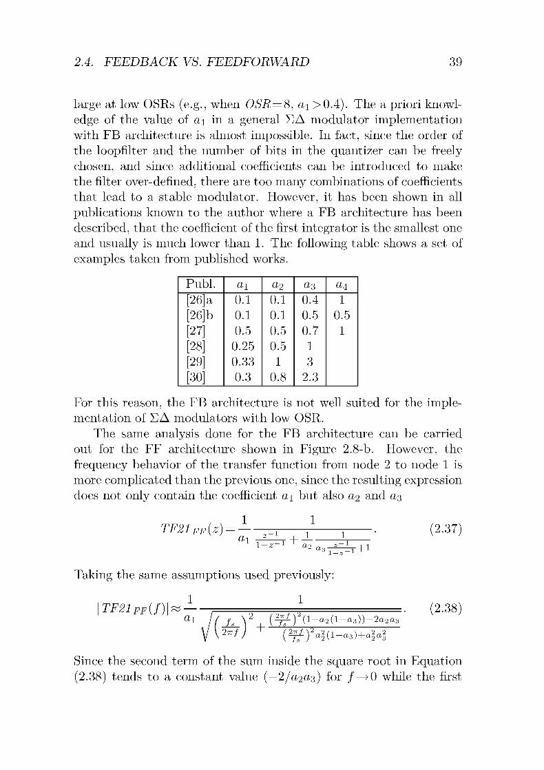
2.4. FEEDBACK VS. FEEDFORWARD 39
large at low OSRs (e.g., when OSR= 8, a\ >0.4). The a priori knowl¬
edge of the value of a\ in a general EA modulator implementationwith FB architecture is almost impossible. In fact, since the order of
the loopfilter and the number of bits in the quantizer can be freely
chosen, and since additional coefficients can be introduced to make
the filter over-defined, there are too many combinations of coefficients
that lead to a stable modulator. However, it has been shown in all
publications known to the author where a FB architecture has been
described, that the coefficient of the first integrator is the smallest one
and usually is much lower than 1. The following table shows a set of
examples taken from published works.
Publ. a\ «2 «3 04
[26] a 0.1 0.1 0.4 1
[26]b 0.1 0.1 0.5 0.5
[27] 0.5 0.5 0.7 1
[28] 0.25 0.5 1
[29] 0.33 1 3
[30] 0.3 0.8 2.3
For this reason, the FB architecture is not well suited for the imple¬mentation of EA modulators with low OSR.
The same analysis done for the FB architecture can be carried
out for the FF architecture shown in Figure 2.8-b. However, the
frequency behavior of the transfer function from node 2 to node 1 is
more complicated than the previous one, since the resulting expressiondoes not only contain the coefficient a\ but also a2 and a3
TF21FF(z)1 1
a\ ±+l;2.37)
0203- - + 1
Taking the same assumptions used previously:
\TF21FF(f)\l l
a\ 2 (^£)2(l-«2(l-a3))-2a2a3fs
2irf —f^-j «2 (1 — a<3) + a<203
;2.38)
Since the second term of the sum inside the square root in Equation
(2.38) tends to a constant value (—2/0203) for /—>0 while the first
40 CHAPTER 2. ARCHITECTURES
term tends to infinity, Equation (2.38) can be further simplified to
1 f\TF21FF(f)\n—27r±- (2.39)
«1 fs
when /<C/S is assumed.
This means that | TF21 FF{f)\ and \TF21 Fß{f)\ have similar fre¬
quency behaviors at very low frequencies. Nevertheless, the two a\
coefficients are not the same, since the FF architecture is the trans¬
position of the FB architecture one expects that if in one case the
coefficient a\ is the smallest and 03 the largest, in the transposed case
a\ will become the largest and 03 the smallest. As a result, the FF
architecture usually ends up with a smaller \TF21 FF{f)\-, and conse¬
quently a better rejection of internal disturbances. Unfortunately, as
/ increases, also the second term of the sum under the square root
in Equation (2.38) starts to have an influence, which is difficult to be
determined a priori.A modulator with this architecture has been carried out during this
research work and will be presented in Chapter 5. It can be anticipatedthat the implemented modulator achieves a | TF21 ff (/)| = —10 dB at
the edge of the signal band by an 8x OSR. Hence, it can be concluded
that the FF architectures have better suppression of the disturbances
generated at the loopfilter internal nodes than the FB architectures.
It is for this reason that FF architectures should be preferred to FB
architectures in broadband EA modulators.
2.5 Conclusions
In Section 2.1 the DT architecture has been preferred to the CT ar¬
chitecture for its much lower sensitivity to the random variation of the
DAC feedback pulse that puts very high specifications on the clock
jitter of CT modulators with high fs.The benefit of the single-loop architecture of having lower sensitiv¬
ity than the cascaded architecture to the imperfections of the analog
building blocks, has make the former be preferred to the latter in Sec¬
tion 2.2. More precisely, single-loop architectures are insensitive to
the finite open-loop gain of the OTAs, these are difficult to achieve,when fast deep sub-micron technologies are used.

2.5. CONCLUSIONS 41
Since the singlebit quantizer generates a large amount of quanti¬zation noise that prevents high DRs being achieved at low OSRs, in
Section 2.3 the multibit architecture has been preferred to the singlebitarchitecture. The use of the DEM method has then been suggestedto cope with the problem of the nonlinearity of multilevel DACs.
Finally, in Section 2.4 the FF architecture has been preferred to
the FB architecture because of its lower sensitivity to the loopfilterinternal disturbances at low OSRs.
For these reasons the architecture that has turned out to be best
suited for the implementation of broadband EA modulators is DT,is single-loop, makes use of a multibit quantizer, and has a loopfilterwith FF topology. This combination does not represent an absolute
optimum since, as it has been shown, other architecture classes have
benefits that this architecture does not have. Nevertheless, this archi¬
tecture represents the best trade-off for the broadband requirements.
Although the above mentioned architecture definition strongly lim¬
its the spectrum of the selectable implementations, there are still many
different individual realizations that can be designed. Hence, the re¬
sult of this analysis represents only a starting point for the designsthat will be presented in Chapter 4 and in Chapter 5.
The next chapter will study the effects of the DAC nonlinearityon the overall performance of the EA ADC.


Chapter 3
DAC Distortion
The feedback DAC is one of the most important elements in a EA A/Dconverter with internal multibit quantizer. As stated in Chapter 2,the DR of the system depends directly on its linearity. It is a rule
of thumb to require that the linearity of the DAC is at least as goodas the resolution of the system. This rule is quite inaccurate for such
a critical element. This chapter shows an attempt to determine the
kind of distortion introduced by a nonlinear DAC.
3.1 System Definition
x[k] xn[k]Loopfilter
yh[k] Quantizer y[k]
Figure 3.1: Block diagram of the EA modulator with nonlinear DAC.
The starting point of this analysis is a generic single-loop EA
modulator with a loopfilter transfer function H{z) (see Figure 3.1).
43

44 CHAPTER 3. NONLINEAR DAC
To simplify the analysis, the quantizer has been assumed perfectlyuniform and with only 1.5 bits; its equivalent linear gain is Gq (seeSection 1.1.1). The DAC has consequently three output levels; its
approximate gain is Ga-
i^yÂ/
/
1-
-jr-it / :
81 /
/ i
/ i
• i *-
1 À, i ^^
'-1' /' 0' '+1' yi /
i /
i /
A/_ -1/>/
/
Figure 3.2: Transfer characteristic of a trilevel nonlinear DAC.
The characteristic function of the non-linear trilevel DAC is plot¬ted in Figure 3.21. The horizontal axis represents the digital inputs,which have been written in quotes, to point out the fact that theyare taken from a finite set of integers, the vertical axis represents the
analog output levels which can vary slightly over the given range and
have instead been written without quotes. To be perfectly linear the
DAC requires its three points to be exactly aligned. The nonlinearityis then described by the displacement e of the central level from the
line drawn connecting the two external points.
The block diagram of Figure 3.1 can be modified without loss of
generality to the diagram illustrated in Figure 3.3. Where eA and eQ
are the DAC and the quantizer linearity errors.
eQ[k] is obtained by subtracting the quantizer input and output
value at time k. e^f/c] is calculated by taking the distance to the ideal
straight line of the DAC output level at time k. The DAC linearityerror is related to y[k] by
eA[k]=fA(y[k}), (3.1)
1For the sake of completeness it must be observed that a nonideal DAC can also
generate a DC error. However, the DC error does not create distortion therefore,
Figure 3.2 can be considered generic although the line drawn connecting the two
external points goes exactly through the origin.

3.2. ASSUMPTIONS 45
Loopfilter
yh[k] leo[k] y[k]
GB> (+
yX[k] TeA[k]
Figure 3.3: Block diagram of the EA modulator with nonlinear DAC.
t öa= fA(y)
jf-a
-x-
'-r '0' '+r y
Figure 3.4: Trilevel DAC linearity error eA as a function of the
output yia
where /a(-) is illustrated in Figure 3.4. Since the DAC output levels
at y— ±1' are exactly on the straight line /^('il') = 0 while since the
central point is shifted by e, /^('O') = e.
3.2 Assumptions
The model described in the previous section cannot be solved analyt¬
ically since it contains nonlinear blocks and can only be described by
implicit equations. The following sections will introduce three impor¬
tant simplifications.
3.2.1 DAC Error Shift
The block diagram shown in Figure 3.5 is equivalent to the diagramshown in Figure 3.3. The former has been obtained by adding e^f/c] to
the output node incoming path and subtracting it to the two outgoing

46 CHAPTER 3. NONLINEAR DAC
Loopfiltereo[k]eA[k] eA[k]
y'h[k] 11 _1 y[k]
yX[k]
Figure 3.5: Equivalent block diagram of the EA modulator with non¬
linear DAC.
paths. Because in practical implementations the resolution of the
quantizer is low (n<4 bit) while the accuracy of the DAC is high
(>10 bit), eQ[k] ^>eA[k]. Hence, e^f/c] can be considered negligible
compared to ecf/c]. The influence of e^f/c] in the loop can therefore
be canceled. The resulting simplified block diagram is illustrated in
Loopfiltereo[k] eA[k]
y'h[k] 1 .1 y[k]
yX[k]
Figure 3.6: Approximated block diagram of the EA modulator with
nonlinear DAC.
Figure 3.6.
The consequence of this operation is that the initial EA modulator
with non-linear DAC is converted into a modulator with ideal DAC
followed by an additive error which is function of the modulator output
itself
y [k] = y'A[k]-eA[k]
eA[k] = fA{y'A[k]).
(3.2)
(3.3)
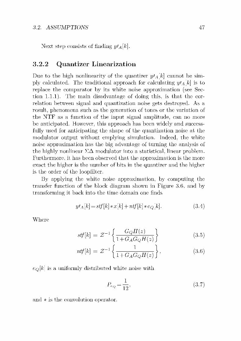
3.2. ASSUMPTIONS 47
Next step consists of finding yia [k].
3.2.2 Quantizer Linearization
Due to the high nonlinearity of the quantizer yfA[k] cannot be sim¬
ply calculated. The traditional approach for calculating yfA[k] is to
replace the comparator by its white noise approximation (see Sec¬
tion 1.1.1). The main disadvantage of doing this, is that the cor¬
relation between signal and quantization noise gets destroyed. As a
result, phenomena such as the generation of tones or the variation of
the NTF as a function of the input signal amplitude, can no more
be anticipated. However, this approach has been widely and success¬
fully used for anticipating the shape of the quantization noise at the
modulator output without emplying simulation. Indeed, the white
noise approximation has the big advantage of turning the analysis of
the highly nonlinear EA modulator into a statistical, linear problem.
Furthermore, it has been observed that the approximation is the more
exact the higher is the number of bits in the quantizer and the higheris the order of the loopfilter.
By applying the white noise approximation, by computing the
transfer function of the block diagram shown in Figure 3.6, and by
transforming it back into the time domain one finds
yrA[k] = stf[k]*x[k] + ntf[k]*eQ[k]. (3.4)
Where
GAGQH(z
e<Q [k] is a uniformly distributed white noise with
1
peQ = yr (3-7)
and * is the convolution operator.

48 CHAPTER 3. NONLINEAR DAC
3.2.3 DAC Error Function
Equation (3.4) cannot be simply substituted in (3.2) because /a(-) is
a function of '-1', '0', and '1', only while yfA[k] in (3.4) has been made
continuous by the means of the white noise approximation. The last
approximation consists in finding a continuous function fA(.) capableof extending the domain of /a(0-
The selection of fA(-) is critical since on one hand it specifies the
kind of distortion introduced by the DAC, on the other hand it defines
the complexity of the resulting equation. A sensible choice for fA(.) is
a function that interpolates fA{*), i-e., that is continuous and equals
/a(.) when 2//^='-l','0','l'. However, as shown in Figure 3.7 there are
f eA= ïa(x)
Figure 3.7: There are many functions capable of interpolating three
points.
infinite expressions fulfilling this requirement.
Since an interpolating function is smooth, i.e., differentiable, it can
be approximated by a Taylor polynomial. Furthermore, since /a(0is symmetric to the vertical axis, fA(-) should be symmetric, as well.
Indeed, there is no plausible reason in having the left and the rightvalue of fA(-) handled in a different way.
The polynomial that satisfies the above requirements is
fcA{x) = e-eSPjatx2% (3.8)%=i
withoo
XX=L (3.9)%=i
3.3. SYSTEM EQUATION 49
Where the symmetry is granted by the choice of an even order polyno¬mial while the agreement of /a(^) and fA(x) at x = —1,0,1 is granted
by (3.9) and by the selection of the e factor.
f eA= ïa(x)
Figure 3.8: Interpolation of the error function for the trilevel DAC.
The solution of (3.8) with
a%-
1 if 1 = 1
0 otherwise(3.10)
is selected here among the infinite a% combinations for the require¬
ment of simplicity. The resulting interpolating expression is then the
quadratic polynomial
fcA(x) = e(l-x2) (3.11)
that is plotted in Figure 3.2.
3.3 System Equation
By combining Equations (3.2), (3.4), and (3.11) one finds
y[k] = stf[k]*x[k] + ntf[k]*eQ[k] —
e(stf[k]*x[k] + ntf[k]*eQ[k])2, (3.12)
where stf[k], ntf[k], and ecf/c] are defined in (3.5), (3.6), and (3.7),respectively.
It can be observed in (3.12) that the first two terms represent the
impulse response of a EA modulator with an ideal DAC, while the re¬
maining terms are the contributions of the linearity error. According

50 CHAPTER 3. NONLINEAR DAC
to the presented model, the DAC nonlinearity generates an intermod¬
ulation of the filtered input signal stf[k] *x[k] and quantization noise
ntf[k] *eQ[k\. The order of the intermodulation is two and is given bythe order of the selected interpolating polynomial.
To demonstrate the validity of the model and the correctness of
the interpolating polynomial, a complete analysis will be carried out
for a EA modulator with a bth order loopfilter.
3.4 5th Order Trilevel-DAC EA Modula¬
tor
3.4.1 Analytical Solution
To find y[k] for a specific EA modulator with a nonlinear trilevel DAC
Equation
y[k]=yfA[k}-fA(yfA[k})1 (3.13)
has to be solved where,
y/A[k] = stf[k]*x[k] + ntf[k]*eQ[k], (3.14)
frA(yfA[k]) = e(l-yfA[k}2)1 (3.15)
and stf[k] and ntf[k] are functions defined by the chosen modulator.
A basic requirement for the STF, in a EA modulator, is that
STF(f)œl for f<fB. Since it is assumed here, that X(f)=0 for
f>fB,
stf[k]*x[k]^^, (3.16)
and Equation (3.12) becomes
yU[k] = ^- + ntf[k]*eQ[k]. (3.17)
Equation (3.17) contains the random signal ecf/c], thus, y[k] has to be
treated as a random signal, as well; to get insight into the statistical
3.4. A 5J H ORDER TRILEVEL-DAC EA MODULATOR 51
properties of y[k], the autocorrelation function Ry has to be calcu¬
lated. The Fourier transformed Sy of Ry will then give the power
spectrum of y[k]. The equation to be solved is
Ry = RylA-e{i-yl*Ay (3-18)
Applying the definition of the autocorrelation function Rx (A.37), one
finds
Ry[k]=E{(yiA[k + .]-e-eyiA[k + .]2)(yiA[.]-e-eyiA[.]2)}1(3.19)
and expanding the brackets, using the linearity of the expectation
value E{}, and with the definition of the crosscorrelation function
CXjV (A.40), one obtains
Ry = RyiA + e Ryi\ ~ 2e RyA IP] + e +
*{Cv>A,v>\+Cy,*A,y,A) -*E{yrA}- (3.20)
The next task will be to solve each term of Equation (3.20) by
substituting yfA with Expression (3.17) and by applying the statistical
properties of ecf/c]. This is a quite tedious mathematical exercise; the
interested reader can find it in Appendix A.l. The result is
_
Rx R*ntf fCx2,x+Cx,x2 2E{x}\y~ G\+ 12 +\ GA GA )
+
(E{x}R*ntf E{x}R*ntfn\ 2(RX, 2RX[0}\
e\GA 3+
GA 6 j+CUi G\ )
2(Ktf Rx.
KtMRM\, 2^
6
V 3 G\+ 6 G\ )+e+
120 144 6 J' l ' '
where R* is the autocorrelation function for energy bounded signals
(A.39).Since, in Equation (3.17), x[k] and ecf/c] are defined by an an¬
alytical and a statistical function, respectively, their lengths can be
infinite. That is the reason why the definitions for E{}, Rx[k], and

52 CHAPTER 3. NONLINEAR DAC
Gx,y[k] for infinite sequences (see Appendix A.4.1) have been used to
calculate Equation (3.21). In contrast to this, if x[k] and ecf/c] are
measured or simulated, their length is finite, since no measurement
or simulation can last forever. This will be the case for the results of
the simulation that need to be compared to Equation (3.21). To sim¬
plify the result comparison, both the analytical calculation and the
simulation result are treated with the same methods. Therefore it is
advantageous to assume that the ideal x[k] and ecf/c] are sequences of
finite length TV and to apply the definitions of Appendix A.4.2. This
does not modify Equation (3.21) as long as,
• x[k] only contains frequencies that are multiples of 1/iV,
• ecf/c], of finite length TV, is still a uniformly distributed white
noise,
N is greater than the length of ntf[k], i.e.,
N-l oo
£wn2=£w]| (3.22)i=0 i=0
If N is large, it can usually be assumed that all three requirements
are satisfied.
By using the discrete Fourier transform (DFT) (see Equation A.46)and by applying the time-frequency pairs of Table A.l, one finds that
2r x ( x x1
Sy~N
X
GA Ga \Ga Ga

3.4. A51H ORDER TRILEVEL-DAC EA MODULATOR 53
where X and NTF are the DFT of x[k] and ntf[k], respectively, Ö
is the Kronecker delta function, and © is the symbol for the cyclicconvolution (see Equation A.48).
Equation (3.23) can be further simplified ignoring the terms with
negligible influence (see Appendix A.2)
\NTF\2S,.
\x\
NG\ 12
\X®X\
~^G\+
\NTF\ \NTF\
12 6
\NTF®NTF\+
E{x}~g7
'KtfM6 2JNÔ +
7?*
Untf [0]:144
KtfM6
RaM
uA+ l No.
(3.24)
The first two terms of Equation (3.24) represent the output spectrum
of the modulator with ideal DAC; the third and fourth term are the
second order intermodulation of x[k] and e^f/c], respectively; the re¬
maining terms are the additional DC components.
The final task will be to substitute GAl Gq, ntf[k], and NTF[n]of the studied modulator, and to solve the resulting expression.
The modulator taken as an example is the one with the trilevel
DAC, 5th order loopfilter, and OSR = 32, designed in Chapter 4; its
loopfilter transfer function is
0.71z"1-2.5z"2 + 3.35z-3-2.04z"4+ 0.48z"5( ô.AO JHz)
1 - 5z"1 + lOz"2 - 10z"3 + 5z"4 - z-
Gq = ^, and GA = 2. The ntf[k] can be obtained by using Equation
(3.6) and by truncating the result at the Nth element; NTF[n] is
calculated by applying the DFT to ntf[k\. The final calculation is
made on a computer.
3.4.2 Simulation Description
The system to be simulated is the one illustrated in Figure 3.1; the
quantizer is uniform and has 1.5 bit, its gain is Gq = \\ the DAC

54 CHAPTER 3. NONLINEAR DAC
1/80/-I
1/32/I
1/7
[kl T_
D --r* D -
!*•
/2
D < *
1/12
D t-D>^> D -
L" \l
Figure 3.9: Loopfilter block diagram of the simulated EA modulator.
is a nonlinear trilevel DAC, with nonlinearity e and gain GA = 2, its
transfer characteristic is shown in Figure 3.2; the block diagram of
the loopfilter H{z) is illustrated in Figure 3.9.
Each iteration of the simulation consists in computing the values
for si...5[i + l] and y/h[i + l] making use of si...s[i], x[i], and y/^KI;y[i + l] is found by quantizing yfh[i + l] while y/^fi + 1] is found by
applying the DAC function on y[i + l]; N iterations are executed.
3.4.3 Results Comparison
The simulation is executed and the power spectrum Sy[n] is obtained
by a DFT. Since, in the calculation of the DFT, it is required that
the signal to be transformed is periodic in TV, a window w[k] needs to
be applied to y[k\. Indeed, y[k] is an a-periodical random sequence.
To make the calculated spectrum comparable to the spectrum of the
windowed y[k], w[k] must also be applied to the calculated spectrum.
This cannot be done in the same way as it has been made for the
simulated y[k] since y[k] does not exist in the calculations. However,it is still possible to apply it, because y[k] and w[k] are statistically
independent. Indeed, using Equation (A.23),
Ry-w — Ry [k\ • Rw [k\, (3.26)
3.4. A51H ORDER TRILEVEL-DAC EA MODULATOR 55
and applying the last time-frequency pair of Table A.l,
DFT{Ry[k]-Rw[k]} = Sy®Sw[n]. (3.27)
Since Sy[n] and Sw[n] still depend on TV, they have been normal¬
ized using Equation (A.50). The final expression for the comparisonis
j^-Sy®Sw^j^-±\DFT{y[k]-w[k]}\2, (3.28)
where the term on the left is given by the analytical calculation, while
the term on the right is given by the numerical simulation.
The comparison has been carried out with
x[k]=Asm(2irfk),
where f = $ and 7V = 215; the nonlinearity of the DAC is e = 0.0001;
w[k] is generated using the Hanning function [36]. To average the
effect of the random e<Q [k], on the power spectrum of the simulated
y[k], the final spectrum has been obtained by averaging the spectra
of 50 simulations, always starting with different initial conditions.
As a first comparison criterion, the SNR curve generated by the
theoretical model and the simulated output spectrum is plotted as a
function of the amplitude A of x[k], the result is shown in Figure 3.10;the gray dots are points of the simulated SNR of the modulator with
ideally linear DAC, the circles are points of the simulated SNR of
the modulator with nonlinear DAC, while the solid line shows the
calculated SNR curve for the modulator, with the nonlinear DAC.
The noise has been integrated over /b=0.8/jv; the DC component
has been discarded in the computation.
It can be observed in Figure 3.10 that the SNR curve can be sepa¬
rated into four regions, with respect to the accuracy of the analyticalestimation. The first region starts at A=—100 dBFS and ends around
A=—70 dBFS, the second region starts at A=—70 dBFS and ends at
A=—20 dBFS, the third region starts at A=—20 dBFS and reaches
A=—5 dBFS, the fourth region covers the remaining part of the curve.
In the first region, the calculated and the simulated SNR match
very well. But, if one considers the power spectrum of y[k] for one
of the input amplitudes in this range (e.g. A=—80 dBFS), shown in
Figure 3.11, it can be observed that the output spectra do not match
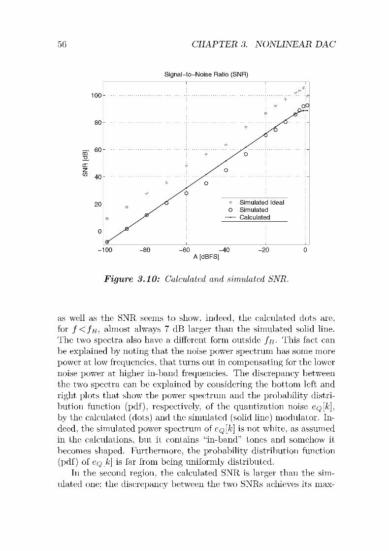
56 CHAPTER 3. NONLINEAR DAC
Signal-to-Noise Ratio (SNR)
100
80
w40
20
0
-100 -80 -60 -40 -20 0
A [dBFS]
Figure 3.10: Calculated and simulated SNR.
as well as the SNR seems to show, indeed, the calculated dots are,
for f <fßi almost always 7 dB larger than the simulated solid line.
The two spectra also have a different form outside fß. This fact can
be explained by noting that the noise power spectrum has some more
power at low frequencies, that turns out in compensating for the lower
noise power at higher in-band frequencies. The discrepancy between
the two spectra can be explained by considering the bottom left and
right plots that show the power spectrum and the probability distri¬
bution function (pdf), respectively, of the quantization noise ecf/c],by the calculated (dots) and the simulated (solid line) modulator. In¬
deed, the simulated power spectrum of ecf/c] is not white, as assumed
in the calculations, but it contains "in-band" tones and somehow it
becomes shaped. Furthermore, the probability distribution function
(pdf) of eQ [k] is far from being uniformly distributed.
In the second region, the calculated SNR is larger than the sim¬
ulated one; the discrepancy between the two SNRs achieves its max-
Simulated Ideal
o Simulated
— Calculated

3.4. A bTH ORDER TRILEVEL-DAC EA MODULATOR 57
c^_ -50
'S
-150
Power Spectrum of y[k]
Simulated Ideal
Simulated
Calculated
10"
Power Spectrum of e [k]
10 10"
FREQ
10"'
pdf of eQ[k]
-4 -3 -2 -1
LOG10(FREQ)
Figure 3.11: Power spectrum of y [k] of the calculated and simulated
modulator; A=—80 dBFS.
imum of 8 dB, when A=—40 dBFS. By considering the power spec¬
trum of y[k] at this input amplitude, shown in Figure 3.12, it can
be observed that the noise floor of the calculated and simulated y[k],inside and outside fß, match quite well, but the simulated spectrum
contains many tones with a considerable amount of power. The dis¬
crepancy of the SNR is due to these tones. Tones are also contained
in the quantization noise power spectrum (plot at the bottom left)and, surprisingly, in the spectrum of y[k] obtained by simulating the
modulator with ideal DAC (gray line). If the tones are ignored, the
simulated power spectrum of ecf/c] becomes more similar to the as¬
sumed spectrum; also the pdf is becoming more similar to the assumed
one, which translates into a better accuracy of the calculation.
In the third region, the calculated and the simulated SNR match
very well. This is the region where the power spectrum of the simu-

58 CHAPTER 3. NONLINEAR DAC
C\l -50
>*
HLL
Q
C\l -100
-150
Power Spectrum of y[k]
x^JuuajSimulated Ideal
Simulated
Calculated
10"
Power Spectrum of e [k]
10 10"
FREQ
10"'
pdf of eQ[k]
-4 -3 -2 -1
LOG10(FREQ) "Q
Figure 3.12: Power spectrum of y[k] of the calculated and simulated
modulator; A=—40 dBFS.
lated and the calculated y[k] are more similar. Indeed, considering the
power spectra of y[k] for A=—5 dBFS, shown in Figure 3.13, it can
be noted that, except for a couple of small tones, the calculated and
the simulated spectra agree almost perfectly. It can also be observed
that, not only the noise floor and the signal component are identi¬
cal, but also the DC component and the second harmonic. Since the
simulated power spectrum of eQ [k] and its pdf match very well with
the power spectrum and the pdf of the white noise approximation,assumed in the analytical calculation, these two last components are
a strong evidence that the polynomial model used to model the DAC
error delivers enough accuracy.
Finally, in the fourth region, the calculated SNR is smaller than
the simulated one; the discrepancy between the two SNRs reaches
a maximum of 3 dB when A=—1 dBFS. By considering the power

3.4. A 5th ORDER TRILEVEL-DAC EA MODULATOR 59
-50
-150
-20 r
Ï. -40
-60 :
^ -80L
Power Spectrum of y[k]
(I
—•-—I I M m4A ft
>**MmW Simulated Ideal
Simulated
Calculated
10"
Power Spectrum of e [k]
10 10"
FREQ
10"'
pdf of eQ[k]
—mmrmmmmim'
-4 -3 -2 -1
LOG10(FREQ) "Q
Figure 3.13: Power spectrum of y [k] of the calculated and simulated
modulator; A=—5 dBFS.
spectrum of y[k] at A=—1 dBFS, shown in Figure 3.14, it can be
observed that, although the signal component, the noise floor, and
the DC component of the calculated spectrum match very well, the
second harmonic component is wrong, since it does not exist in the
simulated spectrum while it is prominent in the calculation results.
This is the source of the 3 dB improvement of the simulated SNR
with respect to the calculated one. The simulated power spectrum of
eQ [k] and its pdf match well with the power spectrum and the pdf of
the white noise approximation; however, not as well as in the previous
case.
3.4.4 Assumptions Discussion
To derive the basic equation (3.12), three major assumptions have
been taken. The first assumption, introduced in Section 3.2.1, neglects

60 CHAPTER 3. NONLINEAR DAC
Power Spectrum of y[k]
c^_ -50-
U<M MQ^> uj.uAjJIjiL**mmnmr
-150-
Simulated Ideal
Simulated
Calculated
10"
cvl. -20 r
"a
£ -40
° -60:z
^ -80L
Power Spectrum of e [k]
•u—m+mmmmtmmqv
10 10"
FREQ
10"'
pdf of eQ[k]
-4 -3 -2 -1
LOG10(FREQ) "Q
Figure 3.14: Power spectrum ofy[k] of the calculated and simulated
modulator; A=—l dBFS.
the contribution of eA[k] in the EA loop. The second assumption was
introduced in Section 3.2.2 and says that the quantizer is a linear ele¬
ment that adds an uncorrelated uniformly distributed white noise to
the input signal. Finally, the third assumption, introduced in Section
3.2.3, extends the domain of the DAC function using a second order
polynomial function. All these assumptions, together, contribute in
making the power spectrum of the calculated y[k] different from the
simulated one.
Considering the results of the comparisons shown in the previous
section, it turns out that the second assumption is a strong source of
error. In fact, the better the power spectrum and the pdf of the sim¬
ulated eq[k] correspond to the assumed ones (i.e., power spectrum is
white and pdf is uniform) the better the calculated and the simulated
power spectra of y[k] match. Further evidence that the first assump-

3.4. A bTH ORDER TRILEVEL-DAC EA MODULATOR 61
Quantizer
Figure 3.15: Dithered quantizer.
c^_ -50
LL
Q
C -loo
-150
-20
o
-40
9 -60
^ -80
Power Spectrum of y[k]
Simulated Ideal
Simulated
Calculated
10"
Power Spectrum of e [k]
10 10"
FREQ
10"
pdf of eQ[k]
A. o
1.5
1
wi——*m**mmmmm0*- 3*°- 0.5
-4 -3 -2 -1
LOG10(FREQ)
-0.5 0.5
Figure 3.16: Power spectrum of y [k] of the calculated and simulated
modulator; A=—80 dBFS; the simulated quantizer is dithered with
-16 dBFS.cr,
&DTH
tion is a strong source of error is that the matching of the spectra
improves when the quantizer is dithered (see Figure 3.15), i.e., when
a random signal is added in front of the quantizer. In fact, by dither¬
ing the quantizer, enj/c] is made "more uncorrelated" with y/h, "more
uniformly" distributed and "more white". This can be observed com-

62 CHAPTER 3. NONLINEAR DAC
paring Figure 3.16 and Figure 3.11. Both figures show the power
spectrum of y[k] for the same input signal (A=—80 dBFS). However,the simulated and calculated data shown in Figure 3.16 match much
better than the corresponding data shown in Figure 3.11.
Power Spectrum of y[k]
WB..Ü npw
-150-
Simulated Ideal
Simulated
Calculated
10
-20 r
Ï. -40
-60 :
^ -80L
Power Spectrum of e [k]
aaMNMM
10 10
FREQ
10
pdf of eQ[k]
o
1.5
1
°- 0.5
-4 -3 -2 -1
LOG10(FREQ)
-0.5 0
e
0.5
Q
Figure 3.17: Power spectra of y[k] of the calculated and simu¬
lated modulator; A=—l dBFS; the simulated quantizer is dithered with
-26 dBFS.(J.
e-DTH
Dithering can improve the matching of many of the spectra shown
in Section 3.4.3 but not of all of them. For instance, it cannot match
the second harmonic of the simulated power spectrum in Figure 3.14
with the calculated one, as illustrated in Figure 3.17. The reason for
the disappearance of the second harmonic may then be one of the two
remaining assumptions and must be further investigated.
To test the first assumption, i.e., to find out if eA[k] has indeed
only a negligible contribution in the loop, the system shown in Fig¬ure 3.18 is simulated and compared to the analytical calculation. To

3.4. A51H ORDER TRILEVEL-DAC EA MODULATOR 63
eA[k]=£(1+y2[k]2)
ec[k]y[k]
^„„LJ,E«(f)|=
fua i
r^ ÇC|*""'
I I. |
Figure 3.18: Block diagram of the modulator with linearized quan¬
tizer and DAC nonlinearity added in the loop.
exclude the effect of the first assumption the quantizer is substituted
with its linear model. In contrast to this, the addition of the DAC
error is left in the loop. The comparison of the resulting spectra, il¬
lustrated in Figure 3.19, shows that since they are almost identical
the third assumption cannot be a major source of mismatch between
the simulated and calculated spectra in Figure 3.17.
The remaining possible cause for the disappearance of the second
harmonic could be the third assumption; i.e., the choice of using a
second order polynomial function to extend the domain of the DAC.
To investigate this, the system shown in Figure 3.20 has been built.
The system consists of a linearized modulator (Modulator 2) using"a real" eQ [k] instead of an uncorrelated uniformly distributed white
noise. The quantization noise cq[/c] is generated by an identical mod¬
ulator with identical input signal (Modulator 1). A problem of this
set up is that, by setting an identical input signal and hence an identi¬
cal quantization noise, also y<±[k] tends to be identical to yi[k\. Thus,
2/2 [k] tends to take only values +1, 0, and —1, without making use of
the extended DAC domain. To prevent this, firstly different random
initial conditions have been taken, secondly the quantizer of Modu¬
lator 1 has been dithered, and finally enj/c] is subtracted from yfh[k]instead of being added.
The spectrum of the simulated 2/2 [&] is illustrated in Figure 3.21; it
shows that despite the use in Modulator 2 of the polynomial extension
of the DAC function the second harmonic is still much lower than the
level anticipated by the analytical calculation. As a result, it can be

64 CHAPTER 3. NONLINEAR DAC
c^_ -50
'S
-150
^ -80
Power Spectrum of y[k]
Sim. (Linearized Mod.
Calculated
10"
Power Spectrum of e [k]
10 10"
FREQ
10"'
pdf of eQ[k]
-4 -3 -2 -1
LOG10(FREQ)
-0.5 0.5
Figure 3.19: Power spectrum of y [k] of the simulated linearized mod¬
ulator and of the calculated modulator; A=—l dBFS.
concluded that also the third assumption cannot be responsible for
the mismatch between the simulated and the calculated spectra in
Figure 3.17.
Since neither the first nor the third assumption can be the source
of the mismatch, the second assumption has to be considered more
carefully. The second assumption not only assumes that the quanti¬
zation error is white and its pdf uniformly distributed, but also that
it is uncorrelated to the input signal. Although the first two charac¬
teristics can be simply checked, by plotting the power spectrum and
the pdf of the simulated ôq [k] the latter characteristic is more difficult
to observe. At the beginning of this section it has been assumed that
dithering is always capable of making the quantization error and the
input signal uncorrelated. Nevertheless, as the modulator input signal
increases, the power of the dithering has to be reduced to prevent the
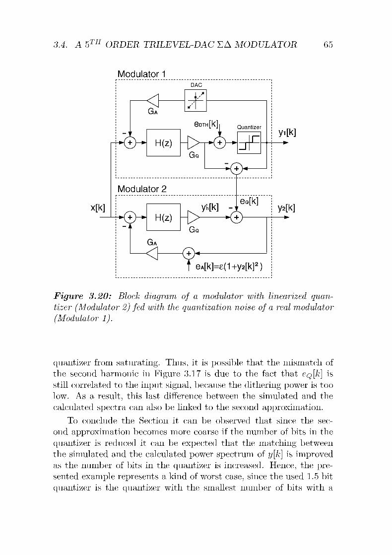
3.4. A51H ORDER TRILEVEL-DAC EA MODULATOR 65
Modulator 1
/"I
DAC
if'
eDT
i -1
Ga
HLk.| Quantizer
S. H(z)
Gq
-W +W rj yiL
i*W"
^kJJ*
J
;r^vModulator 2
y'h[k] -,
eQ[k]r
'^(T^ -
H(z)| Y2[
Go
Ga
CO*\]f eA[k]=8(1+y2[k]2)
Figure 3.20: Block diagram of a modulator with linearized quan¬
tizer (Modulator 2) fed with the quantization noise of a real modulator
(Modulator 1).
quantizer from saturating. Thus, it is possible that the mismatch of
the second harmonic in Figure 3.17 is due to the fact that enj/c] is
still correlated to the input signal, because the dithering power is too
low. As a result, this last difference between the simulated and the
calculated spectra can also be linked to the second approximation.
To conclude the Section it can be observed that since the sec¬
ond approximation becomes more coarse if the number of bits in the
quantizer is reduced it can be expected that the matching between
the simulated and the calculated power spectrum of y[k] is improved
as the number of bits in the quantizer is increased. Hence, the pre¬
sented example represents a kind of worst case, since the used 1.5 bit
quantizer is the quantizer with the smallest number of bits with a

66 CHAPTER 3. NONLINEAR DAC
Power Spectrum of y[k]
c^_ -50-
Sim. (Linearized Mod.)Calculated
-150-
10"
Power Spectrum of e [k]
10 10"
FREQ
10"'
pdf of eQ[k]
-4 -3 -2 -1
LOG10(FREQ) "Q
Figure 3.21 : Power spectrum of y2 [k] of the simulated modulator
with linearized quantizer fed with an eQ [k] generated by a real mod¬
ulator, with dithered quantizer, having the same input signal with
A=-l dBFS.
potentially nonlinear DAC.
3.5 Conclusions
In this Chapter, an analytical method of approximating the effects of
a trilevel nonlinear DAC on the output spectrum of a EA modulator
has been presented. The method is based on three main assump¬
tions, namely, the negligibility of the DAC error in the EA loop, the
quantizer linearity, and the capability of the second order polynomialfunction of interpolating the trilevel DAC linearity error.
To demonstrate the validity of the method, a complete analysis has
been carried out for a EA modulator of bth order and trilevel DAC.

3.5. CONCLUSIONS 67
The main equation has been exactly solved in this case. The calculated
and the simulated power spectra of the modulator output signal y[k]for a pure sinusoidal input have been plotted and compared. The re¬
sults matched quite well although, in certain conditions, discrepancies
were present. The effects of the assumptions taken on the mismatch
between the simulated and the calculated power spectra have been
further studied. Several simulated experiments have pointed out that
the second assumption i.e., the assumption that the quantizer is a lin¬
ear element adding and an uncorrelated uniformly distributed white
noise, is the main source of the mismatch between the calculated and
the simulated power spectra.


Chapter 4
A EA Modulator for
ADSL Standard
Asymmetric digital subscriber line (ADSL) is a telecommunications
standard that uses the plain old telephone service (POTS) to transmit
digital data up to a rate of 8 Mbps [37]. To achieve such a high transfer
rate, the POTS are used up to a bandwidth of 1.1 MHz. Since the
POTS have different degree's of quality and different lengths, discrete
multi-tone (DMT) modulation methods are employed to adapt the
data rate to the characteristic of the transmission medium. Such
adaptability is paid with an increased accuracy in the detection of the
modulated signals. ADSL modems require ADCs with a resolution in
the 13-15 bits range.
Resolution and bandwidth are not the only requirements for an
ADSL ADC. Indeed, the power consumption is also an issue, be it due
to limited available energy in mobile devices, to power limits, e.g., for
bus powered peripheral modems in customer premises equipments, or
to the direct and indirect costs of higher power consumption and heat
generation in central office applications.
This chapter describes the implementation of a EA modulator
with bandwidth, resolution and power consumption suitable for this
kind of application. After showing the selected architecture and de¬
scribing the switch level operation of the implemented filter, the chap-
69
70 CHAPTER 4. A EA MODULATOR FOR ADSL STANDARD
ter will focus on the design of the main analog building blocks. Finally,the experimental results will be reported.
4.1 Architecture
The guidelines for the implementation of a broadband EA modulator
have been given in Chapter 2. According to the conclusions of that
chapter, a broadband EA modulator should have a discrete-time loop-filter with FF topology, be single-loop, and have a multibit quantizer.
The basic concept behind the choice of this architecture was the
conviction that high DR at low OSR and high /s, are achieved bythis class of architecture, with the lowest analog building block re¬
quirements. Since the analog building block requirements are directlyrelated to the quiescent currents and consequently to the circuit power
consumption, the architecture indicated in Chapter 2 can also be ex¬
pected to be the one that leads to the circuit with lowest power con¬
sumption. Hence, the selected architecture should also be suitable for
low power implementations.The guidelines given in Chapter 2 are quite precise, however some
degree of freedom is still left. In fact, the order L of the loopfilter, the
number of bits n of the quantizer, the OSR, and the actual coefficients
of the loopfilter are still freely selectable.
Since multibit quantizers are more complex than singlebit quantiz¬
ers and since they increase the specifications for the circuit providingthe loopfilter output, multibit quantizers are usually not welcomed.
However, it was pointed out in Chapter 2 that their selection is usu¬
ally mandatory in broadband applications, due to the need for a highDR at a low OSR. The selected implementation technology however is
quite fast, providing a fs =80 MHz that by the chosen /jv = 1.25 MHz
results in a not as low OSR= 32. Hence, the constrictions concerningthe number of bits in the quantizer are quite relaxed in this imple¬
mentation; a n=1.5 bit quantizer has been chosen.
The n=1.5 bit quantizer links the advantages of the multibit ar¬
chitecture of having better stability and less quantization noise power,
with the advantages of the singlebit architecture, of being simple and
having low specifications for the circuit providing the signal to the
quantizer.

4.1. ARCHITECTURE 71
The choice for the remaining free parameters will be discussed in
the next sections.
4.1.1 Optimal Loopfilter Order
The optimal loopfilter order L, can achieve the required DR with the
minimum usage of resources, i.e., with the smallest area occupation
and power consumption. In an SC circuit the area occupation and
the power consumption are mainly determined by the values of the
capacitances. In fact, the capacitances usually take a non negligiblearea on the chip and constitute the load to the active components,
defining the quiescent currents and the dimensions of the transistors.
It will be shown in Section 4.3.1 that the values of the capacitances
are inversely proportional to the allowed thermal noise power Pthn hi
fß. Thus, area occupation and power consumption are minimized
when the maximum tolerable noise power Pthn is maximized.
By using Equation (1.11) and solving for Pthn one finds that
^ „
/ SNR SQNR\
Ptfc„ = Pü(lO—nr-10-^ra-J (4.1)
where Px is the power of the full scale input signal, SQNR is the
peak signal to quantization noise ratio, and SNR is the peak signalto noise (thermal plus quantization noise) ratio which for an ideal
system corresponds to the DR. Since the DR is defined by the ADC
specifications and is fix, (4.1) shows that Pthn is increased when Px
and SQNR are also increased. However, there is a trade-off, setting Px
and SQNR since the first usually decreases, while the second increases,
as L increases, and vice versa.
An other consequence of Equation (4.1) is that SQNR has to be
larger than the DR, since Pthn is always positive. Among the loop-filters with L satisfying this requirement a study has been made for
L = 4, 5, and 6. Figure 4.1 shows the result of several simulations
made with EA modulators, with the selected architecture and em¬
ploying loopfilters with the given filter orders. The graph is obtained
by simulating a EA modulator with general architecture, given filter
order and input signal amplitude, and by calculating the SQNR. The
coefficients of the loopfilter are determined by mapping the NTF ob¬
tained with inverse Chebyshev filter function [39]. As a free parameter

72 CHAPTER 4. A EA MODULATOR FOR ADSL STANDARD
Peak SQNR vs. Full Scale Amplitude (OSR=32, n=1.5bit)120
115'
110
105'
m
2,100
ce
0 95CO
1 90'Q.
85
80
75
70-14 -12 -10 -8 -6 -4 -2
Full Scale Amplitude [dBR]
Figure Jf..l: Peak SQNR achievable by single-loop EA modulators
with FF loopfilter topology and with L = A, b, and 6, as a function ofthe full scale input swing.
of the filter function the out of band gain is taken and is increased un¬
til the resulting EA modulator becomes unstable. Then each point of
the graph represents the last SQNR obtained before the loop becomes
unstable. The plot of Figure 4.1 has been obtained by using a filter
with rational coefficients and a topology that includes a loop with
zero-delay. Since the coefficients have to be discretized, to be imple¬mented by capacitor ratios, and the zero-delay loop is removed, when
the NTF is mapped to the selected FF loopfilter topology, the real EA
modulator will be stable for lower maximum input signals thus, it will
achieve lower peak SQNRs. To take these limitations into account the
solutions highlighted in Figure 4.1, have been chosen on the flat part
of the curve, far away from the collapsing region. Furthermore, to the
simulated peak SQNR, 2 dB have been subtracted before substitutingit in Equation (4.1) to calculate Pthn- The following table shows the

4.1. ARCHITECTURE 73
values of Pthn obtained by substituting in Equation (4.1) the points
highlighted in Figure 4.1 relative to Vr.
L Pthn [/Vg\4
5
6
2.38e-10
2.78e-10
1.73e-10
The maximum Pthn is achieved by the EA modulator with L = 5 thus,L = 5 is the optimal filter order and it has been selected for this im¬
plementation.
4.1.2 Zero Placement
NTFs
In-Band Noise >
Reduction /1 \ JF » à
JÊ 1 /jrVÊL * /
JF I if
/
y^ —Z_J ,—1—4_^
:
Frequency Fb — log
Figure J^.2: Notch filter generated by the internal negative feedback
loop.
The shaping capability of every single-loop EA modulator with
L > 2 can be improved by shifting the zeros of the NTF away from
DC such that the quantization noise becomes optimally spread and
minimized over the signal band; the effect is shown in Figure 4.2. In
practice, the zeros are shifted by adding a negative feedback path over
a couple of integrators, as is illustrated in Figure 4.3. The transfer

74 CHAPTER 4. A EA MODULATOR FOR ADSL STANDARD
G(z)=z2- 2z + g + 1
Figure Jf..3: Topology, transfer function, and pole position of the
internal negative feedback loop.
function of the block diagram is
R(z.z2-2z + g + l'
(4.2;
The poles of R(z) are a conjugated complex couple; their position is
given by the vertical line going through z = \ (see Figure 4.3). Because
of the global feedback, the poles of the loopfilter become the zeros of
the NTF(z). For g<Cl the position of the conjugated complex zeros
is very near to the circle with radius one, they therefore implement
an almost perfect notch at the frequency
hVg fs
IT
(4.3)
To find the most convenient position of the zeros the frequency
response of the decimation filter should also be known. In fact, as
illustrated in Figure 4.4 as the decimation filter requires some space to
cut off the upper part of the bandwidth near to the Nyquist frequency
/iv is not available to the input signal. It is therefore convenient
to place the zero in such a way that only the noise in fß < fjy is
minimized. Indeed, the narrower the signal band is the higher is the
minimum quantization noise attenuation i.e., the better is the achieved
peak SQNR.With L = 5, two notches can be implemented in this design. The
choice of the frequency of the two notches has been made for fß =
1.05 MHz; the two frequencies are at 649.747 kHz and 1.006584 MHz,

4.1. ARCHITECTURE
OD
;o
<D
TD
"cO)
CO
Decimation Filter
ShapingImprovement
-f^-->'-
Frequency Fb Fn
Figure 4-4: Optimal zero position.
respectively. The improvement compared to the solution without the
notches is 12 dB.
4.1.3 Filter Coefficients
Figure 4.5: Block diagram of the ADSL EA modulator.
By taking the NTF of the 5th order solution highlighted in Fig¬ure 4.1, mapping it to the FF bth order loopfilter topology, scaling the
internal nodes (limit the signals into the ranges allowed by the am¬
plifier output swings), quantizing the obtained coefficients into ratios

76 CHAPTER 4. A EA MODULATOR FOR ADSL STANDARD
of integers (more accurate to be implemented with ratios of capaci¬
tor), and setting up the internal feedbacks to implement the notches
at the frequencies specified in Section 4.1.2, the EA modulator with
block diagram depicted in Figure 4.5 is obtained. The simulated peak
SQNR is 106 dB when /# = 1.05 MHz; the full scale input signal is
0 dB when referred to the DAC reference level.
Noise and Signal Transfer Functions
10
Frequency [MHz]
Figure 4-@: Noise and signal transfer function of the designed EA
modulator.
The frequency response of the NTF and STF, obtained by makinguse of the the quantizer white noise approximation are plotted Figure4.6.
Figure 4.7 shows that every internal node of the loopfilter has a
transfer function, to the input node, with gain less than 0 dB, in fß.
Hence, every internal disturbance, in fß, is reduced when referred
to the input signal. This allows the requirements of the internal in¬
tegrating stages to be lowered and their power consumption to be
reduced.

4.2. SWITCH LEVEL DESIGN 77
Internal Transfer Functions
20 r
10
0
-10
S -20-
Signal Band
><>o<>
CD
DJ
CO
30
-40-
-50
-60
-70-
-80
+++++++
+
o°°°0o
0<>**<><**>'
$0*0<><>
o<>*ooo00
>*,^D1
, +++-•^j:*+:i++
,oO'>o°
oooooooo
+ o
o
+ o
— NTF110 NTF21o NTF31+ NTF41o NTF51
0 0.02 0.04
f/(fs/2)0.06 0.08 0.1
Figure 4 •7: Transfer function, of the internal nodes, to the input of
the modulator.
4.2 Switch Level Design
The single-ended version of the switch level diagram of the imple¬mented circuit is shown in Figure 4.8. The actual EA modulator
however, has been implemented with a fully differential SC techniquebecause of increased signal dynamic range, higher immunity to clock
and charge feed-through and better substrate noise rejection. The
integrators are operated with two non-overlapping clock phases in
non-inverting mode: during phase (f\ the sampling capacitors Cs%
are charged, while during phase </?2 that charge is transfered to the
integrating capacitor Cpi- The coefficients are realized as capacitor
ratios.
The voltage VVh is obtained by a passive capacitive voltage divider.
During cpi the output of the summing network built of Cffi to Cff5

00
Cfbci
Cfbm
CFBC2
CFBA2
X[k]
cpiD^f
Ç2
CF2
^ITCfbbiCfs
I1|
1CS3
cpid
..92
||^
cpip
?JjN
91^
v\y
920]
fi
(p2o
W
CFF2
CS4
IV
\"l
>J
w\
cpinx
y2**
)i
^91
r\y^
(P2c,N
i
CF4
(P1\TCFBB2
Cf5
Hhn
essHH
XCFF3X
CFF4
""j91
rt^^
(p2D
ï
XCFF5
1.5
bitQuantizer
Tri-levelDAC
y[k]
2V
Vh
92£
Figure
4-&:SC
implementation
oftheADSLEA
modulator.
I > O Ü o o Ü CO Co B I

4.2. SWITCH LEVEL DESIGN 79
settles to
Vyh =T,5t=iVo*CFFt
(44)CpFl + Cpp2 + CpF3 + Cpp4 + Cpp$
where the voltages Vo% are the output voltages of integrator 1 to 5,
respectively. The loss in signal amplitude due to the passive network
can be tolerated because the 1.5 bit quantizer has quite relaxed speci¬fications. The two voltage references of the quantizer are implemented
by connecting the Cq capacitors, previously charged to voltage V^EFand VftEF, respectively between the output of the loopfilter VVh and
the input node of the corresponding comparator. The latter starts its
regeneration at the end of cpi and it is designed to be fast enough to
have its output settled for the beginning of </?2, so that the reference
branches can either be directly, crossed, or not connected at all to the
input of the first amplifier, depending on whether the input of the
quantizer was lower than V^EF, greater than V^EF or between V^EFand VftEF. The factor of two at the output of the D/A in Figure 4.8
is obtained by cross coupling the reference branches connected to the
reference voltages V^ and V^.The inner feedback loops to establish the NTF notches are im¬
plemented by T-cell structures [50] that with the implemented filter
coefficient
_
CfbaCfbc 1_ ,. _n
Cfba + Cpßß + Cpßc Cp
achieve large ratios despite low capacitor spread.All the used capacitance values are multiples of the unit capaci¬
tance CM = 0.1 pF and are listed in Table 4.1.
To reduce the effect of the signal dependent charge injection, de¬
layed phases (Ç\d and cf2D have been used [16]. To further reduce
the amount of charge involved, the switches with delayed phases are
transmission gates with NMOS and PMOS transistors of equal size.
Figure 4.9 shows the circuit for the generation of the non-overlapping50% duty-cycle two-phase clock. Phase TpT^ and Tp2~5 are requiredto toggle the PMOS switches used in the transmission gates. The
supplementary delaying block AT\ and AT2 increases the time avail¬
able to the comparator for regenerating and the time available to the
amplifiers for integrating, respectively. With this architecture of the
clock generator the input clock signal is 2fs.

80 CHAPTER 4. A EA MODULATOR FOR ADSL STANDARD
i 1 2 3 4 5
CSt [pF] 0.5 0.5 0.2 0.2 0.1
CFl [pF] 3.5 0.8 0.4 0.8 1.2
Cpp% [pF] 0.5 0.4 0.3 0.2 0.2
Cfbäi [pF] 0.1 0.1
Cfbbi [pF] 0.2 0.8
Cfbc* [pF] 0.1 0.1
Cß [PF] 0.5
^Q [PF] 0.5
Table 4-l; Values of the used capacitors.
D Qh
^o b> Q
r-AT2-
~> >>—P^T^0q)i 0 q)iD 0 q)iD
Figure 4-9: Non overlapping two-phase clock generator.
The design of the input stage and of the quantizer will be explainednext.
4.3 Input Stage Design
As shown in Chapter 2, in the selected set of EA architectures the
noise and distortion performance is determined primarily by the noise
and distortion performance of the input stage. The implementationof an input stage capable of achieving the specified performance is
therefore the most important task of the design.

4.3. INPUT STAGE DESIGN 81
4.3.1 Capacitor Sizing
Among the several noise sources present in an SC circuit, the most
important are represented by the switches. The thermal noise power
Pc, sampled on a switched capacitance C, is approximately white and
is equal to the thermal noise power generated in fs/2 by an equivalentresistor with resistance [41]
1
(4-6)Req~~faC-
thus, the power sampled on the capacitor is
Pc = 4kTReq2
2kT
~C~ (4.7)
where k is the Boltzmann constant and T is the absolute temperature.
Cr y-i9)Vro
C+f
Figure 4-10: Switch level diagram of the input stage.
The employed stage (see Figure 4.10, [40]) has four switched ca¬
pacitors namely, C<t, Co, C^, and C^. With (4.6) and (4.7), one
finds that the noise, generated in fß sampled on Cg and Co, and on
C^ and CR is
P<Cs 2-2kT
CsOSRand PcR = 2
2kT
CrOSR1(4.8)

82 CHAPTER 4. A EA MODULATOR FOR ADSL STANDARD
respectively. Referring both noise contributions to the input node
gives
p-=^+iPc«=cSj(1+ä)- (4-9)
Since Cs = Cr here (4.9) simplifies to
RkT
By assuming that the noise power of all but the first integrator are
negligible, the requirement for Pthn is given by
Pthn<PxlO-^. (4.11)
To obtain at least 14 bit of resolution a DR>86 dB is required (seeEquation (1.10)). Since the modulator is stable for input signals with
swing up to the value of the DAC reference level, here chosen to be
Vr = Vr —Vft =1.6 V, and since each signal swing is doubled by the
fully differential circuit architecture
1.62P* =— (4-12)
Thus, by substituting Equations (4.12) and (4.9) in (4.11), and by
solving for Cs, one finds that Cr = Cs~ 0.5 pF and Cf = 3.5 pF.
4.3.2 OTA Offset Requirements
Since the load of the amplifiers used in SC circuits is capacitive,
the most commonly used type of amplifier is the operational tran¬
simpedance amplifier (OTA). In usual input stage implementations,the OTA input offset is not a critical parameter, since it merely trans¬
lates into a supplementary DC term that is easily compensated. How¬
ever as it will be shown next, in the used input stage implementationthe offset of the OTA turns out to be one of the main sources of the
DAC nonlinearity.The circuit to be analyzed is shown in Figure 4.11; it is the input
stage of Figure 4.10 without the signal branches. Indeed, the signalbranches do not have a direct influence on the linearity of the DAC.

4.3. INPUT STAGE DESIGN 83
(1+ocr)Cr
Vro
Vr°
(1+aF)CF
Figure 4-H; Switch level diagram of the DAC with the analyzed
asymmetries.
Three main sources of asymmetry have been introduced namely, the
mismatch of the reference capacitors cxr, the mismatch of the in¬
tegrating capacitors ap, and the input referred OTA offset voltage
Vos- These are not the only three sources of asymmetry in a real
case, indeed, the asymmetrical charge injection due to the mismatch
of the switches, to the mismatch of the parasitic capacitors, and to
the mismatch of the phases falling edge steepness, can also contribute
to the harming of the symmetry. However, these effects are difficult
to quantify and furthermore, as it has been observed in the measure¬
ments, they have a negligible effect compared to previously mentioned
sources.
The first step of this analysis is the calculation of AVq , AVq, and
AVq i.e., the variations of the OTA output voltage Vo for y = +l,
y = 0, and y = —l, respectively. Due to these asymmetries the cir¬
cuit cannot be simplified into a single-ended version and the obtained
variations are quite complex indeed,
AV+1 -2VRCR {l + ctR)CR + {l + aRF)CFCF {l + a'RF)CR + {l + aF)CF
vCr {l + ctR){CR + Cp)
+ OS
Cp {l + a'RF)CR + {l + aF)CF(4.13)

84 CHAPTER 4. A EA MODULATOR FOR ADSL STANDARD
AVS
AVö1
0
2VR
(4-14)
CR {l + aR)CR + {l + a'RF)CFCF {l + a'RF)CR + {l + aF)CF
CR {l + aR)CR + CF+Vos
CF {l + ct'RF)CR + {l + ctF)CF(4.15)
where a'RF = (cvr + ap + ctRCtp)/'2 and aRF = (cvr + ap)/2. Equations
(4.15), (4.14), and (4.13) allow the characteristic function of the tri¬
level DAC to be plotted (see Figure 4.12) and the nonlinearity factor,
Figure 4-l%: Transfer characteristic of the nonlinear DAC.
as defined in Chapter 3, to be calculated
AV^ + AVn1 -2AKo
2AF+1(4.16)
Then, by substituting (4.15), (4.14), and (4.13) in Equation (4.16)and by assuming
one finds that
aR,aF <C 1,
Vos < VR,
aRaF {l + aF)CF-{l + aR)CR Vos
{Cr + CfY 2VR
(4.17)
(4.18)
Equation (4.18) shows that e is mainly determined by the ratio2V~-
The contribution of the, already small, aR and cïf can be considered
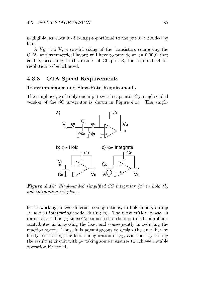
4.3. INPUT STAGE DESIGN 85
negligible, as a result of being proportional to the product divided byfour.
A Vr = 1.6 V, a careful sizing of the transistors composing the
OTA, and symmetrical layout will have to provide an e~ 0.0001 that
enable, according to the results of Chapter 3, the required 14 bit
resolution to be achieved.
4.3.3 OTA Speed Requirements
Transimpedance and Slew-Rate Requirements
The simplified, with only one input switch capacitor Cs, single-endedversion of the SC integrator is shown in Figure 4.13. The ampli-
a)
Vl (Di 9S CD2
/<P2 />
b) cpi- Hold c) cp2- IntegrateCf
CsT fl>^ Vo ViCp ft
Figure 4-13: Single-ended simplified SC integrator (a) in hold (b)and integrating (c) phase.
fier is working in two different configurations, in hold mode, during
</?i and in integrating mode, during cf2- The most critical phase, in
terms of speed, is </?2 since Cs connected to the input of the amplifier,contributes in increasing the load and consequently in reducing the
reaction speed. Thus, it is advantageous to design the amplifier by
firstly considering the load configuration of </?2, and then by testingthe resulting circuit with cpi taking some measures to achieve a stable
operation if needed.

86 CHAPTER 4. A EA MODULATOR FOR ADSL STANDARD
The operation of the OTA can be separated into two modes, in
slewing mode, the OTA is a constant current source Iß, with an input
and output capacitance Cgs and Co, respectively while, in settling
mode, it is an ideal transconductance gm with the same input and
output capacitances. The equivalent circuit of the integrator for each
OTA operating mode is shown in Figure 4.14. The step response of
a) Slewing Mode
Cf
b) Settling Mode
CfVg
Cs •gs Ib©
Co Cs /gs Vggm®
Co
Figure 4-14: Equivalent circuit of the slewing (a) and settling (b)mode.
the simplified integrator is shown in Figure 4.15. At the first instance,
Figure 4-15: Transient response of the OTA output during the inte¬
grating phase.
due to the direct capacitive Vj —> Vb path,
Cp CsvS=Vj
where
Cf + Co Cs + Cgs + Cp||Co
CpCoCf\\Co
Cp + Co
(4.19)

4.3. INPUT STAGE DESIGN 87
Then, if the input step is sufficiently large, the OTA operates in slew¬
ing mode and the charge sitting on the capacitors is sunk by a constant
current Iß ; the slope of Vb is given by the slew rate
SR=lB
. (4.20)^L, slew
where
CL,slew=Co+CF\\(Cs + CgS). (4-21)
After a while, the OTA input voltage Vg has been reduced so much
that the OTA begins to operate in settling mode; Vb takes an expo¬
nential form with time constant
Tsetti=^îL, (4.22)9m
where
CL,setti=Co + CF^Co(Cs + Cgs), (4.23)Uf
and converges to
VSr = ~V!. (4.24)Up
Since the settling operation is exponential, Vq° is achieved onlyafter an infinite amount of time. Thus, a residual error esetti. is always
present at the end of cf2 if the duration of cf2 is finite. Determiningwhat is the maximum eseui., tolerated by the EA modulator, is very
important for the definition of the SR and the Tseui. of the OTA. The
more accurately the SR and rsetti. can be determined, the more tighttheir values will be and the less current will the OTA consume. How¬
ever, this is not a simple task since it implies the selection of more
complicated circuit models that have to be applied to the full EA
modulator by an extensive use of behavioral simulations. Further¬
more, this approach is risky since it is always possible to forget the
contribution of a parasitic element and then to specify too tight values
for the SR and the rseui.. However, Geerts [42] and Burger[43], in their
thesis, have successfully used this approach in the implementation of
two 3th order, single-loop, EA modulators.

88 CHAPTER 4. A EA MODULATOR FOR ADSL STANDARD
The requirement set up here is that eseui, relative to the step
size Vq° ,when Vj is maximum, must be less than half of the least
significant bit (LSB) of the entire EA ADC, i.e.,
e^tL i__V°? 2
y J
Only if this requirement is satisfied can one be completely sure that the
system will not be able to detect the integration error, independentlyfrom what the source of the error is.
Since Vb at the end of </?2 is given by
l-Asettie-—y (4.26)
T'settl
eSetti=VSrAsettie~T^r (4.27)
where TseUi. is the duration and —Vq°(1 — Asetti.) is the initial condi¬
tion, of the settling curve. Substituting (4.27) in (4.25) gives
TsettL < TT^ü—,in , i' t a T• (4.28)
0.69(n + l)+ln (Asetti.)
Unfortunately both, Tseui. and Asetti. are unknown, furthermore theycan be considered fitting parameters of the settling curve since the
used model assumes that there is a well know instance where the
OTA stops to slew and begins to settle; in reality, this instance does
not exist since the transition from one mode to another is smooth.
However, with some further simplifications this model can lead to a
useful lower bound. Firstly, since Vb is already near to Vq° when
the settling phase begins, Asetti. is less than one. Nevertheless, Asetti.
is still in the order of magnitude of one thus, \n(Asetti.)~0 can be
assumed without losing too much in accuracy and without increasingthe bound. Equation (4.28) becomes then
Secondly, one can define a lower bound for rsetti. by assuming that,for a duration Tsiew the OTA brings Vb to approximately Vq° , oper¬
ating in slewing mode, and for the remaining time Tsetti. it converges

4.3. INPUT STAGE DESIGN 89
to exactly Vq°, operating in settling mode (see Figure 4.15). This
assumption gives the following condition for SR
Gm=^^max s ( i \ _£ ) (4 30)Tglew Cp \ (CF+Co)(Cs + CgS+Cp\\Co) J
where V/;max is the maximum Vj and
Tsiew=T(p2—Tsetti.. (4-31)
Considering the system of equation composed by (4.29), (4.30),and (4.31) it becomes clear that there is only one free parameter
namely, Tsetti.- Furthermore, Tseui. sets a trade-off between the set¬
tling and the slewing requirements, that can be optimized to exploitthe full advantages of the used integration technology. Indeed, because
of Equation (4.31), if Tsetti. is increased to reduce the requirements on
Tsetti., Tsiew is decreased and the requirements on the SR increased,and vice versa.
In the input stage of this design Cp = 3.5 pF, Cs = 1 pF (the sum of
the two input capacitors), V/)max = 1.2 V, the estimated CffS = .5 pF,the estimated Co = l pF, n«14 bit, and T(f>2=b ns (assuming that
T(f>1 = 5 ns and giving a budget of 2.5 ns for the two time slots between
the two non-overlapping phases, Ts = 12.5 ns); Tsetti. and Tsiew have
been chosen to be 3.75 ns and 1.25 ns, respectively. Substituting the
given numbers in Equations (4.30) and (4.29) gives S'A = 600 V/psand rsetti. =355 ps. Substituting DR in Equation (4.20) gives 7b=~
1.23 mA while the given Tsetti. corresponds to an integrator dominant
pole at frequency fPcl =450 MHz.
4.3.4 Finite Switch ON Resistance
The calculations of the previous section assume that the switches are
ideal. Among the characteristics of a switch its ON and OFF resis¬
tances are of great importance. The advantage of the MOS transistor,used as a switch, is that it is an almost ideal open connection when
it is in the OFF state. In contrast to this, the resistance in the ON
state is not zero and depends on many design parameters such as the
over drive voltage, the channel size and the used technology.
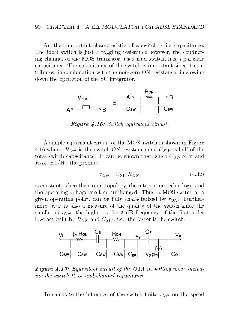
90 CHAPTER 4. A EA MODULATOR FOR ADSL STANDARD
Another important characteristic of a switch is its capacitance.The ideal switch is just a toggling resistance however, the conduct¬
ing channel of the MOS transistor, used as a switch, has a parasitic
capacitance. The capacitance of the switch is important since it con¬
tributes, in combination with the non-zero ON resistance, in slowingdown the operation of the SC integrator.
Vh Ao-
-*B Csw
Ron
-^wv- -oB
Csw
Figure 4-16: Switch equivalent circuit.
A simple equivalent circuit of the MOS switch is shown in Figure4.16 where, Ron is the switch ON resistance and Csw is half of the
total switch capacitance. It can be shown that, since Csw^W and
Ron ocl/W, the product
T~ON = CswRoN (4.32)
is constant, when the circuit topology, the integration technology, and
the operating voltage are kept unchanged. Thus, a MOS switch at a
given operating point, can be fully characterized by ton- Further¬
more, ton is also a measure of the quality of the switch since the
smaller is ton, the higher is the 3 dB frequency of the first order
lowpass built by Ron and Csw, i.e., the faster is the switch.
Vi ßx RonCs Ron
-J\AAr-Vg
Cf
Csw Csw Csw Csw >gs Vggm
Vo—o
Co
Figure 4-17: Equivalent circuit of the OTA in settling mode includ¬
ing the switch Ron and channel capacitance.
To calculate the influence of the switch finite ton on the speed

4.3. INPUT STAGE DESIGN 91
of the SC integrator, the schematic shown in Figure 4.14-b, analyzedin Section 4.3.3, has been extended with the switch model. The re¬
sulting circuit is depicted in Figure 4.17. The parameter ßT has been
introduced to point out the fact that the switch on the left and on
the right side of Cs can have a different operating point and can be
also implemented by a different type of switch and therefore can have
a different ton-
By considering Figure 4.17, it can be noted that the displayedcircuit can be slowed down in two ways, with respect to the switch
characteristic. By setting up a too large Csw or a too large Ron -
The optimum Ron is then given by
, 2ton(Co + Cf)
RoN>opt-xlcscF9m(ßr+iy (433)
and, by substituting Ron,opt back into the expression for the domi¬
nant closed loop pole
Pc'-°pt =Co + (Cs + Cga)(l+ColCF) + CT
(434)
CT = gmroN(ßr + l) | l + 2\l2Cs{1 + Co/CF\ßT + l]9mJON
(4-35)
Where CT = 0 for tov = 0. Equation (4.34) will be used later to test
the degradation of the OTA settling speed due to the switch non-
idealities and (4.33) will be then used to size the switches for maximum
settling speed.
4.3.5 OTA Architecture
A fully differential telescopic OTA [44] with regulated cascode [45][46] [47] has been selected to implement the OTA; the schematic is
shown in Figure 4.18; the common mode feedback is dynamic [48] and
is applied to the gates of transistors M7 and Ms. The auxiliary ampli¬fiers OPi and OP2 are implemented with two fully differential, folded
cascode OTA [49] with PMOS and NMOS transistor input differen¬
tial pairs, respectively; The common mode feedback is implemented

92 CHAPTER 4. A EA MODULATOR FOR ADSL STANDARD
91
91
0)2
Vb
—^^
C3 Ci
M7 M8
^ 92
VOUT*o
VlN
.M3
Ml
3 C
J +À
i +x
J C
OPi
©lb
©2 k
C2
OP2tM5 Met
M4
92
C4
-cpi
1vc
M2
Figure 4-l&: Schematic of the main OTA.
by tail transistors, operating in the linear region [50]; the schematic
is shown in Figure 4.19. Due to the five stacked MOST, this archi¬
tecture has a limited output swing and a poor input common mode
range, these are not real problems in an SC integrator.
The design strategy for the optimal sizing of the amplifier transis¬
tors is given in [43].With a current consumption of 3.9 mA, of which 2.4 mA are spent
in the main amplifier and the rest in the regulating amplifiers, the im¬
plemented OTA has gm = 16 mS and lb = 2A mA. By substituting the
open loop characteristics of the OTA in Equations (4.20) and (4.22)one finds that SX=600 V/ps and fPcl=870 MHz. By using Equa¬tion (4.34), instead fPcl>opt = 638 MHz, where t0at = 1.65 ps (NMOSswitches) and /?T = 2.45 (ration between ton of the NMOS switches
and ton of the transmission gates). The last bandwidth seems to be
still quite high compared to the basic requirement calculated in Sec¬
tion 4.3.3, but the basic requirement must be held also at worst case
operating conditions i.e., Vdd =2.2b V, T=85°C, and slow technol-

4.4. QUANTIZER DESIGN 93
TL r
Figure 4-19: Schematic of the auxiliary OTAs.
ogy. Since the performance degradation of the switches is very highin worst case conditions (up to 100% increment in ton), Pel has to be
set with a good margin.
4.4 Quantizer Design
The less uniform is the multibit quantizer, the less stable is the EA
modulator. Indeed, a non-uniform quantizer generates more quanti¬zation noise power than a uniform quantizer1. Hence, the maximum
input signal power has to be reduced to keep the quantizer input in
the conversion range.
The quantizer in the chosen architecture is not critical from this
point of view, since it only contains two comparators with two thresh¬
olds. Two thresholds are simply implemented in differential circuit
architectures by changing the circuit connections and using only one
reference voltage. Hence, only one voltage is required to define the
characteristic of the quantizer. This voltage is provided externally
1This can be intuitively understood considering that any quantizer can be
interpreted as a non-uniform quantizer of higher resolution which is so non-uniform
to have some of its levels joined together.

94 CHAPTER 4. A EA MODULATOR FOR ADSL STANDARD
here so that the comparator uniformity is corrected externally de¬
spite random comparator offsets. This is advantageous for the passive
implementation of the sums of the loopfilter feedforward paths since
the resulting signal with reduced swing and consequently the reduced
quantizer reference voltages do not increase the offset requirements.
With the selected capacitor sizes and ratios, in accordance with the
modulator block diagram shown in Figure 4.5, and with Vr = 1.6 V,
Vref = Vref ~ Vref = 26 mV. The voltage has to be provided differ¬
entially and with a common-mode compatible with the comparator
input common-mode swing.A more critical requirement for the quantizer in this implementa¬
tion is its speed, more precisely its regeneration speed. As already
pointed out in Section 4.2, the time from the starting of the regenera¬
tion phase, to the time when the quantizer output is needed, is short.
Indeed, it is the time slot between the end of cpi and the beginning of
cf2- Section 4.4.1 will show the architecture of the implemented com¬
parators that is specially suitable for fast regenerating comparators.
A further problem of a general quantizer is its hysteresis i.e., the
dependency of the current decision from the previous one. With the
adopted architecture this type of problem can be considered negligible,since all the voltages in the comparator and in the following logic are
always the same before the beginning of the regeneration phase.
4.4.1 Comparator Architecture
The comparator used in this design is depicted in Figure 4.20. It
consists of a differential input pair (Mi, M2), two current mirrors
(M3-M5, M^-Mq), an NMOS latch circuit, and a synchronizing logic.The NMOS latch is composed of two n-channel transistors (M7, Ms)with cross-connected gates and an n-channel switch (Mq) for resetting.The dynamic operation of this circuit is divided into a reset time and a
regeneration time. The two operations take place near to the edges of
(f\. When cpi rises, switch Mq is closed, the current that flows through
Mq forces the previous two logic state voltages to be equalized. Duringthe rest of cpi the latch acts as a resistive load for the differential pair
Mi, M2 and the output tracks the input. In the meanwhile, the inputof the AND stages is set to zero and the output of the comparator
is brought to the logic state zero, independently of what the voltage

4.4. QUANTIZER DESIGN 95
A A
Figure 4-%0: Schematic of the implemented comparator.
level on the latch is. The regeneration time is initiated by the openingof M9, i.e., by the falling edge of (f\. The voltage settled on M9 at
this instant acts as an initial imbalance for the regeneration operationcarried out by transistors M7 and M&. After a while, when M7 and
Ms have already begun to regenerate, the input of the AND stages is
set to one and the AND connected to the rising terminal sets to one.
The output of the comparator will remain valid until the next reset
operation will start i.e., until cpi will return to one.
To maximize the speed of the regeneration time, the parasitic ca¬
pacitance at nodes A and B has to be minimized. This mainly impliesthe minimization of the interconnecting capacitances, the minimiza¬
tion of the area of transistor Mg and of the transistors composing the
two AND gates. The input load of the AND gates can be optimized
considering the fact that, during the regeneration time, they are onlyallowed to go from zero to one and not vice versa.
The trade-offs in the design of the NMOS latch are pointed out in
[51].
4.4.2 Feedback Logic
The feedback logic must be simple since it is also in the critical path;it has to synchronize the output of the comparators with cf2 and to

96 CHAPTER 4. A EA MODULATOR FOR ADSL STANDARD
generate the signal that goes to the DAC switches. The feedback logicis implemented by the circuit shown in Figure 4.21 where Q+ and
Q+ are the outputs of the comparator sensing the quantizer positivethreshold and Q~ and Q~ are the outputs of the comparator sensingthe quantizer negative threshold.
Figure 4-%l: Logic used to generate the digital feedback signal.
4.5 Experimental Results
The EA modulator has been implemented in a digital 0.25 pm CMOS
process with six layers of metals and one layer of polysilicon. No spe¬
cial option for the implementation of precise capacitors is available.
The capacitance density achieved by capacitors implemented with a
six metal sandwich is 0.22 fF/rmi2. The bottom plate stray capaci¬
tance is 12% of the main capacitance. The nominal supply voltage is
2.5 V.
The chip photomicrograph is depicted in Figure 4.22. A pseudo-differential layout strategy [16] has been adopted. A regular field of
squares is clearly visible in the upper side of the chip, it is composedof 266 unit capacitors with capacitance 100 fF, it contains every used
switched capacitor and some dummy structures. The switches are
positioned below the capacitors, with the bus of digital signals, that
occupies the entire width of the core but have a height of no more
that two unit capacitors. The OTAs are placed below the switches.
The OTA of the input stage is at the left side and occupies one third
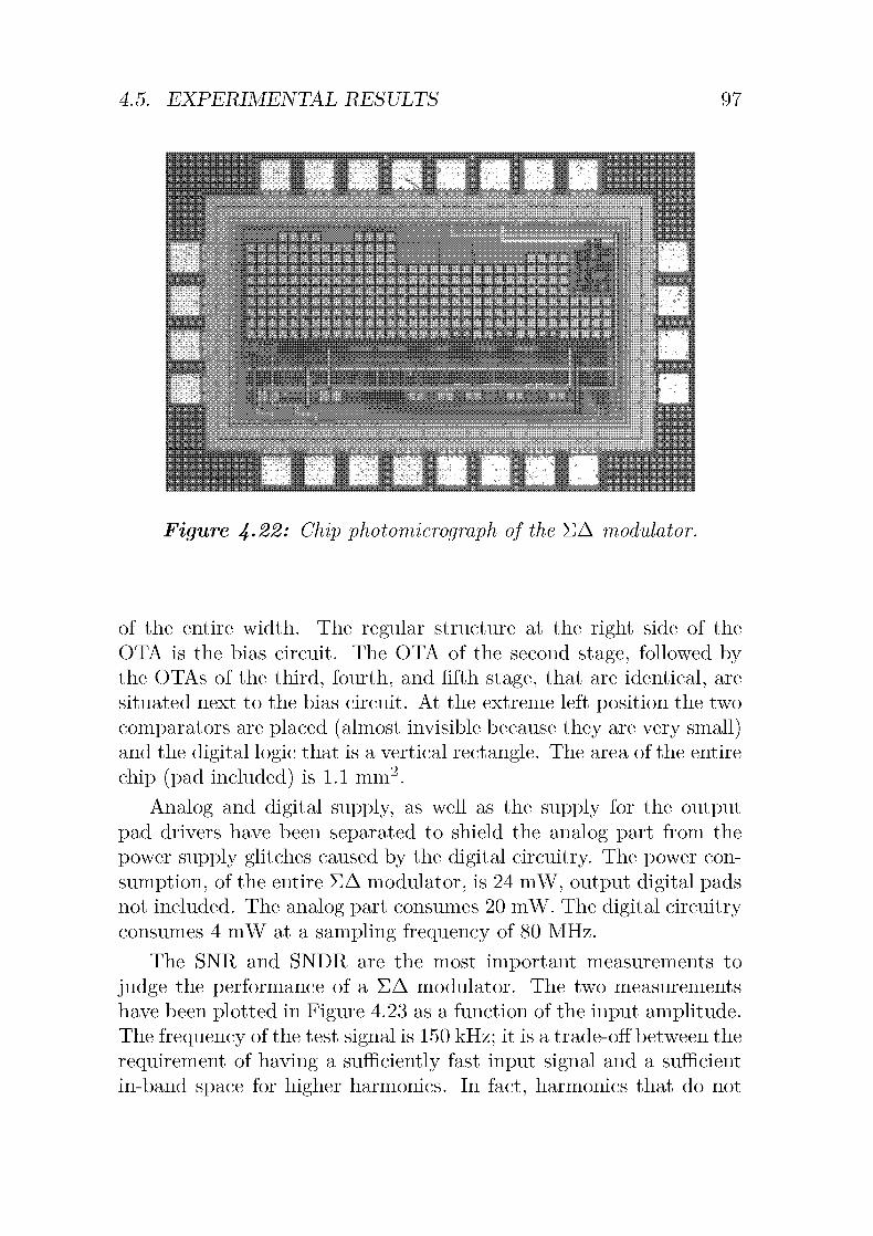
4.5. EXPERIMENTAL RESULTS 97
Figure 4-22: Chip photomicrograph of the EA modulator.
of the entire width. The regular structure at the right side of the
OTA is the bias circuit. The OTA of the second stage, followed bythe OTAs of the third, fourth, and fifth stage, that are identical, are
situated next to the bias circuit. At the extreme left position the two
comparators are placed (almost invisible because they are very small)and the digital logic that is a vertical rectangle. The area of the entire
chip (pad included) is 1.1 mm2.
Analog and digital supply, as well as the supply for the output
pad drivers have been separated to shield the analog part from the
power supply glitches caused by the digital circuitry. The power con¬
sumption, of the entire EA modulator, is 24 mW, output digital padsnot included. The analog part consumes 20 mW. The digital circuitry
consumes 4 mW at a sampling frequency of 80 MHz.
The SNR and SNDR are the most important measurements to
judge the performance of a EA modulator. The two measurements
have been plotted in Figure 4.23 as a function of the input amplitude.The frequency of the test signal is 150 kHz; it is a trade-off between the
requirement of having a sufficiently fast input signal and a sufficient
in-band space for higher harmonics. In fact, harmonics that do not

98 CHAPTER 4. A EA MODULATOR FOR ADSL STANDARD
80
S* \
70
0D
— SNR
—- SNDR
S 60
g 50
co 40 \
oc
z 30en
1
1
1
20
10
0/ DR = 88 dB
-! :
-80 -60 -40 -20
Signal Power [dBFS]
0
Figure 4.23: Measured SNR and SNDR of the EA modulator.
fall into the signal band are not, as in Nyquist converters, aliased back
but they add to the out of band quantization noise and are filtered
out. The DR of the converter can be read on the x-axis of Figure 4.23
when the SNR crosses the zero-dB horizontal line; it is 88 dB. The
peak SNR is 85 dB and the peak SNDR is 79 dB. An example of a
measured spectrum is shown in Figure 4.24; the input amplitude is
-3 dBFS; the measured SNR is 83 dB and the SNDR is 77 dB. The
chip has been tested in a standard, 44 pin, JLCC package.
Since the measured noise floor is as low as the noise floor, calcu¬
lated by sizing the sampling capacitors, it can be assumed that the
nonlinearity of the DAC is lower than e = 0.0001. However, in certain
circumstances the effects of the nonlinearity can be observed. E.g.,when the input signal is a simple DC level, tones are internally gen¬
erated. This can be seen in the measured spectrum shown in Figure4.25 indeed, three tones can be observed, in the signal band, althoughthe input signal is a DC signal. The magnitude of the highest tone is
less than -90 dBFS.

4.6. SUMMARY 99
Modulator Ouptut Spectrum
10 10 10
frequency [MHz]
10
Figure 4-%4: Example of measured output spectrum.
The measured results are summarized in Table 4.2.
4.6 Summary
The design of a 2.5 MS/s, 14 bit EA modulator with 32x OSR is de¬
scribed in this chapter. The modulator employs a bth order loopfilterwith two internal feedback loops and a 1.5 bit quantizer. The switch
level diagram of the implemented modulator is described. The de¬
sign of the input stage is analyzed carefully; the effects of the circuit
non idealities on the linearity of the trilevel DAC are calculated; the
desired DR is achieved using the smallest possible capacitor area; a
simple flow for determining the requirements of the OTA is presented;
a method to optimally size the circuit switches is shown.
The Measured performance is very similar to the calculated one,
and the 14 bit of resolution have been achieved. The total power

100 CHAPTER 4. A EA MODULATOR FOR ADSL STANDARD
Modulator Ouptut Spectrum
10 10
frequency [MHz]
Figure 4-25: Effect, on the output spectrum, of the DAC nonlinear¬
ity.
consumption is 24 mW, this is, by far, the lowest power consumptionachieved up to now by a EA modulator with such high combination of
resolution and bandwidth. A comparison of the power consumptionof published EA modulators, as a function of the maximum SNR, is
plotted in Figure 4.26. The low power consumption shows that that
this architecture is more suited for broadband implementations than
the architectures used in the previously published converters.

4.6. SUMMARY 101
DR
Peak SNR
Peak SNDR
Input Range
88 dB
85 dB
79 dB
3.2 Ypp diff.
ÎB
fsOSR
1 MHz
80 MHz
32
Power SupplyPower Consumption
2.5 V
24 mW
Process
Chip Area
0.25pm Single-Poly6 Metal CMOS
1.1 mm2
Table 4-2: Characteristics of the EA modulator.
Power vs. Peak SNR Comparison1 1
o(7)-
0(6)
(4)
o(5)(4MS/S)
This XA
Modulator!
"70 75 80 85 90 95
SNR [dB]
Figure 4-%6: Consumed power, as a function of the peak SNR, of
published EA modulators. (l)-[52], (2)-[53j, (3)-[54j, (4)-[55j, (5)-[56], (6)-[57j, (7)-[30j.
300
250
| 200
§ 150
oQ_
100
50
n
-
c
°(3)
o(2)°(1)
•


Chapter 5
A EA Modulator for
VDSL Standard
Very high bit-rate digital subscriber line (VDSL) is a telecommunica¬
tion standard that has been developed to support exceptionally high-bandwidth applications, such as high-definition television (HDTV).VDSL can achieve data rates up to approximately 30 Mbps over voice
on a single twisted-pair copper loop [58] [59]. This makes VDSL the
fastest available form of DSL. Like most DSL technologies, the per¬
formance of VDSL depends significantly on the physical distance tra¬
versed by wiring: shorter distances mean faster networking. Such level
of speed and channel adaptability require A/D Converters capable of
achieving resolutions up to 14 bit and conversion rates of more than
20 MS/s.This set of requirements represents a significant challenge for a
EA ADC. To give an idea of how these specifications compare to the
existing implementations, it can be observed that the fastest EA mod¬
ulator implemented in a CMOS technology published so far has a con¬
version rate of only 12.5 MS/s and a resolution as low as 11 bits [30].This chapter demonstrates the implementation of a 14 bit, 25 MS/sEA modulator.
After showing the selected architecture and describing the switch
level implementation, this chapter focuses on the requirements and
103
104 CHAPTER 5. A EA MODULATOR FOR VDSL STANDARD
the implementation of the main analog building blocks. Finally the
experimental results are reported.
5.1 Architecture
Like the EA modulator described in Chapter 4, this modulator also
makes use of the design guidelines of Chapter 2.
Since the integration technology used to implement this circuit is
one generation newer than the technology used for the the ADSL ADC
in Chapter 4, the sampling frequency is chosen so as to be about twice
as high. A fs = 200 MHz is taken that implies 8x OSR at the specifiedconversion rate of 25 MS/s. Due to the low OSR, a n = 4 bit quantizer
is chosen here to achieve the required DR. The selected value of n is
the result of a trade-off between the improvement of the quantizer
linearity and the increment in circuit complexity.
5.1.1 Optimal Loopfilter Order
The method used to select the optimal order of the loopfilter is based
on the same principles as those described in Section 4.1.1 i.e., the
minimization of the input switched capacitor. However this time, to
define a first guess for the loopfilter transfer function, the CLANS1
method, illustrated in [60], is used. The CLANS method determines
the position of the NTF poles by maximizing the loopfilter noise shap¬
ing capability while keeping the ||L|| i norm of the NTF in the specified
range. The CLANS method turns out to be superior to the simpledetermination of the NTF, by using an inverse Chebyshev filter func¬
tion adopted in Section 4.1.1. However, it is limited to modulators
with large n (n>2).After having considered the performance of loopfilters with order
L = 5, 6, generated with slightly different parameters, L = b has been
chosen because of better stability and sufficient noise shaping. The
NTF used as a starting point for the design of the current loopfilter,achieves 96 dB of peak SQNR, being stable for input signals with
amplitude up to -4 dB the DAC reference level.
1Closed-Loop Analysis of Noise Shaping Coders

5.1. ARCHITECTURE 105
5.1.2 An Ideal Pipelined Resonator
Section 4.1.2 has shown that the shaping capability of the single-loopEA modulator, can be improved by realizing a notch in the signalband. In practice, the notch is implemented with a resonator in the
loopfilter transfer function H(z).Section 4.1.2 has shown how to implement a resonator with the
poles placed on the vertical line tangents to the unit circle, with its
center in the origin. However, a real resonator requires the poles to
be exactly on the unit circle. As long as the resonant frequency is
low (i$^2 2)' ^ne P°les obtained with the method of Section 4.1.2,
are near to the unit circle and the quality of the obtained resonator
is good. However, as the resonant frequency increases, the distance
of the poles from the unit circle increases. As a result, the qualityof the resonator gets worse and the capability of the correspondingNTF notch to suppress the quantization noise decreases. This effect
can be observed in Figure 4.6, where the notch at the lower frequency
(649.7 kHz) is deeper than the notch at the higher frequency (1 MHz).With the even lower OSR used in this design, the relative frequen¬
cies of the required resonators are higher than in Chapter 4. Hence,the quality and the noise suppression capability of the resulting NTF
notches give a poor result. Thus, real resonators with poles on the
unit circle are used, instead. The topology of the selected resonator
preserves the pipelined structure of the filter, despite the realization
of a two-integrator loop with only one overall delay. The basic idea
is to use integrator blocks with only half a delay each. The block
G(z)=z2- z(2-g) + 1
Im' Pole
/
i
"**x Pos.
-1\ J Re
Figure 5.1: Block diagram of the ideal resonator composed by two
integrators with half clock delay.

106 CHAPTER 5. A EA MODULATOR FOR VDSL STANDARD
diagram is shown in Figure 5.1. The transfer function of the obtained
resonator is
and its pole frequency is
/ff = arctan [ —^- ] . (5.2;
The two resonators implemented with the selected L = b loopfil¬ter have their pole frequencies being optimized for /b=0.85</jv; theyare at frequency 6.34 MHz and 9.86 MHz, respectively. As the first
notch is sufficiently low it is still implemented by a standard two-delay
resonator, while the second notch is implemented by the described
one-delay resonator.
5.1.3 Filter Coefficients
The next step in the loopfilter design requires three operations. At
first the NTF has to be mapped to the used filter topology. Secondlythe internal states have to be scaled in accordance to the amplifier
output swings. Finally the filter coefficients have to be quantized.The latter of the listed operations is by far the most difficult and
time demanding one, since the stability and the noise shaping capabil¬
ity of the filter can be strongly modified. However, the result of this
operation is extremely important in obtaining a well designed EA
modulator. Indeed, achieving small coefficient ratios is convenient for
simplifying the SC filter implementation. Furthermore, the stabilityof the modulator can be further improved by manually varying the
loopfilter transfer function.
The block diagram of the final architecture is illustrated in Fig¬ure 5.2. The ideal resonator is implemented by the last two integra¬
tors, while the second and third integrators implement the standard
approximated resonator. Compared to the ADSL modulator whose
block diagram is shown in Figure 4.5, this modulator has all the FF
paths anticipated by half a clock cycle. This is needed to reduce the
speed specifications of the comparator regeneration time and of the
DAC related digital logic.
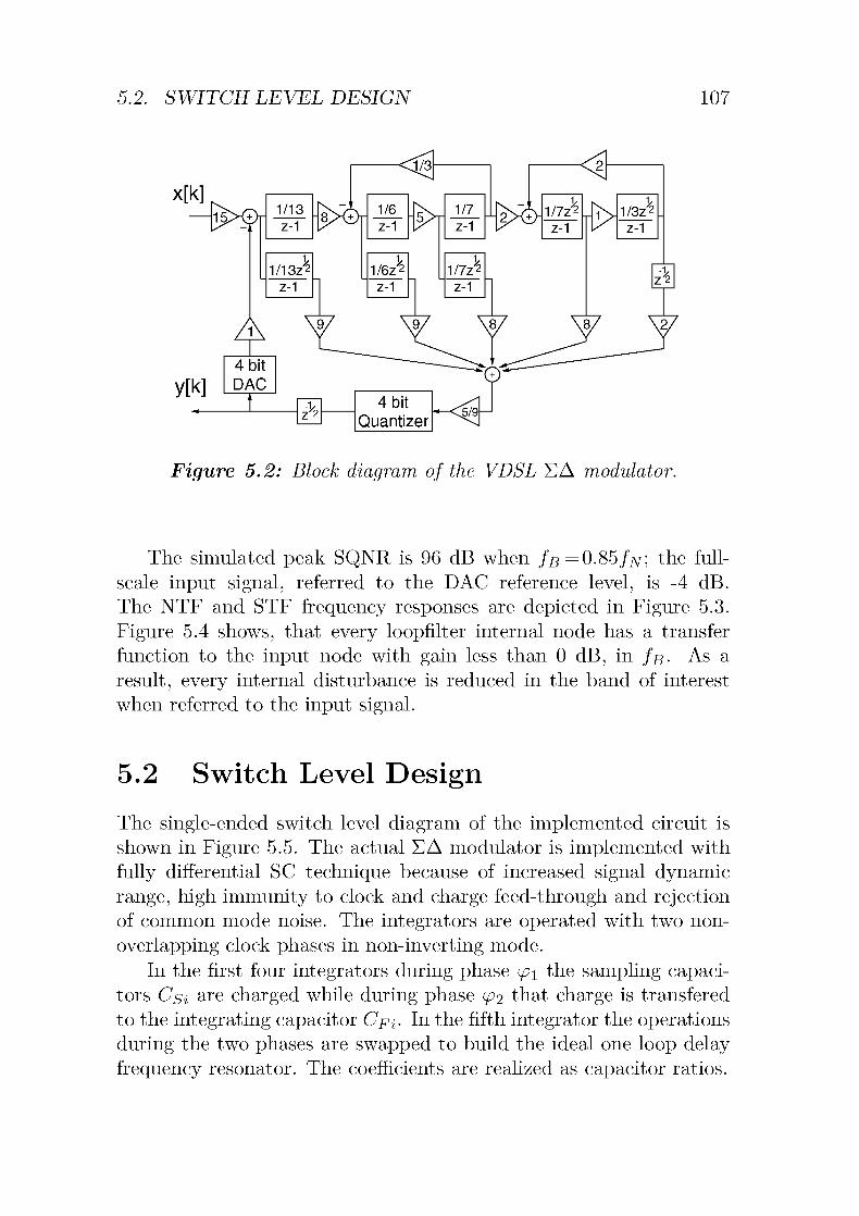
5.2. SWITCH LEVEL DESIGN 107
Figure 5.2: Block diagram of the VDSL EA modulator.
The simulated peak SQNR is 96 dB when /s=0.85/]v; the full-
scale input signal, referred to the DAC reference level, is -4 dB.
The NTF and STF frequency responses are depicted in Figure 5.3.
Figure 5.4 shows, that every loopfilter internal node has a transfer
function to the input node with gain less than 0 dB, in fß- As a
result, every internal disturbance is reduced in the band of interest
when referred to the input signal.
5.2 Switch Level Design
The single-ended switch level diagram of the implemented circuit is
shown in Figure 5.5. The actual EA modulator is implemented with
fully differential SC technique because of increased signal dynamic
range, high immunity to clock and charge feed-through and rejectionof common mode noise. The integrators are operated with two non-
overlapping clock phases in non-inverting mode.
In the first four integrators during phase cpi the sampling capaci¬
tors Csi are charged while during phase </?2 that charge is transfered
to the integrating capacitor Cp%. In the fifth integrator the operations
during the two phases are swapped to build the ideal one loop delay
frequency resonator. The coefficients are realized as capacitor ratios.

108 CHAPTER 5. A EA MODULATOR FOR VDSL STANDARD
40
20
ÊÊ -20
CÛ
« -40
-60
-80
-100
-120
10"
Noise and Signal Transfer Function
NTF
STF
10u 10'
Frequency [MHz]
10
Figure 5.3: NTF and STF of the EA modulator.
The loopfilter output voltage VVh is obtained by a passive capac¬
itive voltage divider. During cp2 the output of the summing network
built of CpFi to Cpp5 settles to
VJ2i=l VoiCFFi
VhCppi + Cpp2 + Cpp3 + Cpp4 + Cpp5
(5.3)
where the voltages Vo% are the output voltages of integrator 1 to
5, respectively at the end of the (f2- Compared to the ADSL EA
modulator, the loss in signal amplitude due to the passive network
cannot be tolerated in this design, because of the quantizer higherresolution. A gain stage with gain G that amplify VVh is therefore
introduced between the loopfilter output and the quantizer input.
A resistor ladder with identical unit resistors Ru builds up the
voltage references that are sampled on capacitors Cq's during cpi and
added to the gain stage output voltage during cp2- The resulting signal

5.2. SWITCH LEVEL DESIGN 109
Internal Transfer Functions
20 r
10
0
-10
£-20CD
Signal Band
,0<>0
CO
30
-40
-50
-60
-70
-80
Yö +o
V°
ö
o °0 +
-ü +++++o +
^^^oooooooooooooooooooooooo.
-^.ô-. _++, D.°ö5PJl.°P.a.PnöxicLn.[iöD.QBE>Bnft +<
+ + + +
â +Oooo0o«H +o
.anxiixQ.cxa aaBE^a
°0o°ooooooooooooooooooooo
. _ . _ NTF110 NTF?1D NTF,1+ NTF410 NTF51
0 0.05 0.1 0.15 0.2 0.25 0.3 0.35
f/(fs/2)0.4
Figure 5.4- Transfer function, of the internal nodes, to the input ofthe modulator.
is then sensed by the 15 comparators that are regenerated at the end
of (f2- The outputs of the latter are mapped through the logarithmicshifter to the switches at the unit capacitors bottom terminals. The
connection to either V^ or V^ is individually selected. The compara¬
tor and the logarithmic shifter must be sufficiently fast to have their
outputs settled for the beginning of the next (f2-
At the same time, the comparator output goes to the input of
the DEM block building up the next controlling signal for the loga¬rithmic shifter, which is changed at end of the next cf2- The binary
representation of the quantizer output y[k] is calculated, as well and
sent to the output. The DEM logic and the logarithmic shifter im¬
plement the data weighted averaging (DWA [61]) algorithm used to
average the DAC linearity error generated from the mismatch of the
unit capacitors.
The values of all the used capacitances are listed in Table 5.1.

CS2
Til
Cfbi
CF2
I1|
1CS3
Mrs
CFB2
CF3
(P2d^[
q\p>
\q)2D
(pIC),
|Cp2
(P2D^[
(P^rb
15^
cpiD
\q)2D
(P1D
(P1D
CS4
'Uhr
h'
(piD
CF4
1>D
CF5
I1|
1CS5
92
p.q)
2DM
cpi
<p2°
L<pi
Lf-/^
KPid
1(P2
|vC^
CFF2
JCf
f3~|~\q)2D
cpiD
Cff4~|~
CFF5
\q)2D
Logarithmic
Shifter
4bitQuantizer
4>
y[k]
,^_
DEM
15
(P1
i^>u"^H^"
GainStage
V
Vh
r cpi
92
Figure
5.5:SC
implementation
oftheVDSLEA
modulator.
i I Ol > O Ü o o CO
Co 1

5.2. SWITCH LEVEL DESIGN 111
i 1 2 3 4 5
CSt [pF] 0.25x15 1.2 0.5 0.2 0.1
CFl [pF] 3.25 0.9 0.7 0.7 0.3
CpF% [pF] 0.45 0.45 0.4 0.4 0.1
Cfb% [pF] 0.05 0.2
Cq [pF] 0.3
Table 5.1: Values of the used capacitors.
Due to the 1.8 V supply voltage, the overdrive of the samplingswitches is too small to make the time constant negligible at fs =
200 MHz. Bootstrapping is therefore used in the input stage to make
the settling accuracy signal independent. The charge pump used is
Switch
Figure 5.6: Charge pump schematic.
shown in Figure 5.6 [62]. In the remaining stages, transmission gates
with NMOS and PMOS transistors, having their size optimized for
minimum switch time constant are used, instead. The switches con¬
nected to the amplifier inputs are simple NMOS transistors. Boot¬
strapping is also used for the cpi and (p\p> switches in the quantizer to
reduce the capacitive load of the reference resistor chain. The selected
charge pump circuit is shown in Figure 5.7 [63]. Delayed phases (p\p>
and (f2D reduce the effect of the signal dependent charge injection

112 CHAPTER 5. A EA MODULATOR FOR VDSL STANDARD
M4 Vi Ms Vbs,cik-o
Vclk
Figure 5.7: Charge pump schematic to achieve a Vdd+Vt boot¬
strapped voltage.
[16].The circuit selected for the generation of the non-overlapping two-
phase clock is almost identical to the one shown in Figure 4.9. Since
no critical operation is executed during the time slot between two
phases, ATi=0. In contrast to this, to increase the duration of </?2
and reduce the specifications of the analog building blocks in the most
critical phase, AT2>0.
The requirements and the implementations of the used circuit
block will be explained next.
5.3 Input Stage Design
The selected input stage is a single-capacitor stage. This means that
the same sampled capacitance is used to sample both, the input signaland the voltage reference. The fully differential switch level diagram of
the stage is shown in Figure 5.8. The ideal variation of the differential
integrator output Vb, at the end of </?2 at time /c + 1, is given by
AVo[k + l]=Vo[k + l\-Vo[k]Cp
Vx[k]2g/[fc]-15
15VR
(5.4)where 0<y[/c]<15 is the quantizer output at time k while Vx[k]V£[h]-V£[k] andFß: n VR are the differential input signal at
time k and the DAC voltage reference, respectively.

5.3. INPUT STAGE DESIGN 113
Vxo-
Vxo-
Vro Vro+
(p1D (p2(14)\(p2(14)\Csu14
Vro Vr
cpiD q)2(i)\ cp2(i))l (P2(1)\ Csui
VSo Vr
cpiD q)2(o)\ q)2(o)/
)\ (P2(0)\ CSUO
"~s.~
cpiD q)2(o)/ q)2(o)0)/ (p2(0)/
vsA vs*CsuO
(p1D (p2(1)/ (p2(1);yn es
Vr^ Vr^u1
cpiD q)2(i4)/q)2(i4)
Vcmin
(p1?
Cf
92
VcminCf
Vr6 Vr6
^Vo
^V5
Figure 5.8: SC diagram of the input stage.
5.3.1 Capacitor Sizing
To size the capacitors of the input stage, it is assumed that their
switching noise dominates over any other noise source. The noise
power, sampled on a switched capacitor C in /jv, is given by Equation
(4.11). In the chosen input stage (Figure 5.8), there are 30 capacitorswith capacitance Csu, each with a noise transfer function
TFis.(*:Csu
Cp
1
[z-r(5.5)
According to (4.7), every capacitor contributes to the total noise power
with
Pt2kT
CsuaSu
(5.6)

114 CHAPTER 5. A EA MODULATOR FOR VDSL STANDARD
Since the input signal x[k] is sampled on 15 capacitors together, the
square of the transfer function of x [k] is
^KI^îiV (5-7)
Hence, by assuming that the noise of each capacitor is uncorrelated,one finds that the total input referred noise power, in /jv, turns out
to be
th"-
TF\(z) -15CS„-(5-8)
Since in this design Vr = 1.2 V and since the modulator is stable
for input signals up to -4 dB of Vr, the full scale signal power is
By substituting Equations (5.8) and (5.9) in (4.11) and by solvingfor Csu one finds that to achieve 14 bit of resolution 6^^250 fF is
required. Consequently, Csi=3.75 pF and Cpi = 3.25 pF.
5.3.2 Capacitor Matching Requirements
In the selected input stage the linearity of the DAC is mainly deter¬
mined by the matching capability of the used unit capacitors. The
capacitance of the ith unit capacitor CSu% can be expressed as
CL=(l + *l)Csu (5.10)
where Csu is its nominal value and aSt (i = 0...14) is the relative
variation. By calculating AVo including the effect of the capacitor
mismatch one finds that the error, i.e., the difference between the
ideal and the real AVo is
ic^ v^ asi+asi v^ asi+asi
eAV°=—c^rVR is ' (5'n'
A is the set of the indexes of y [k] capacitors selected by the used DEM
algorithm, while A is the set of the indexes of the remaining y[k] —15
capacitors.
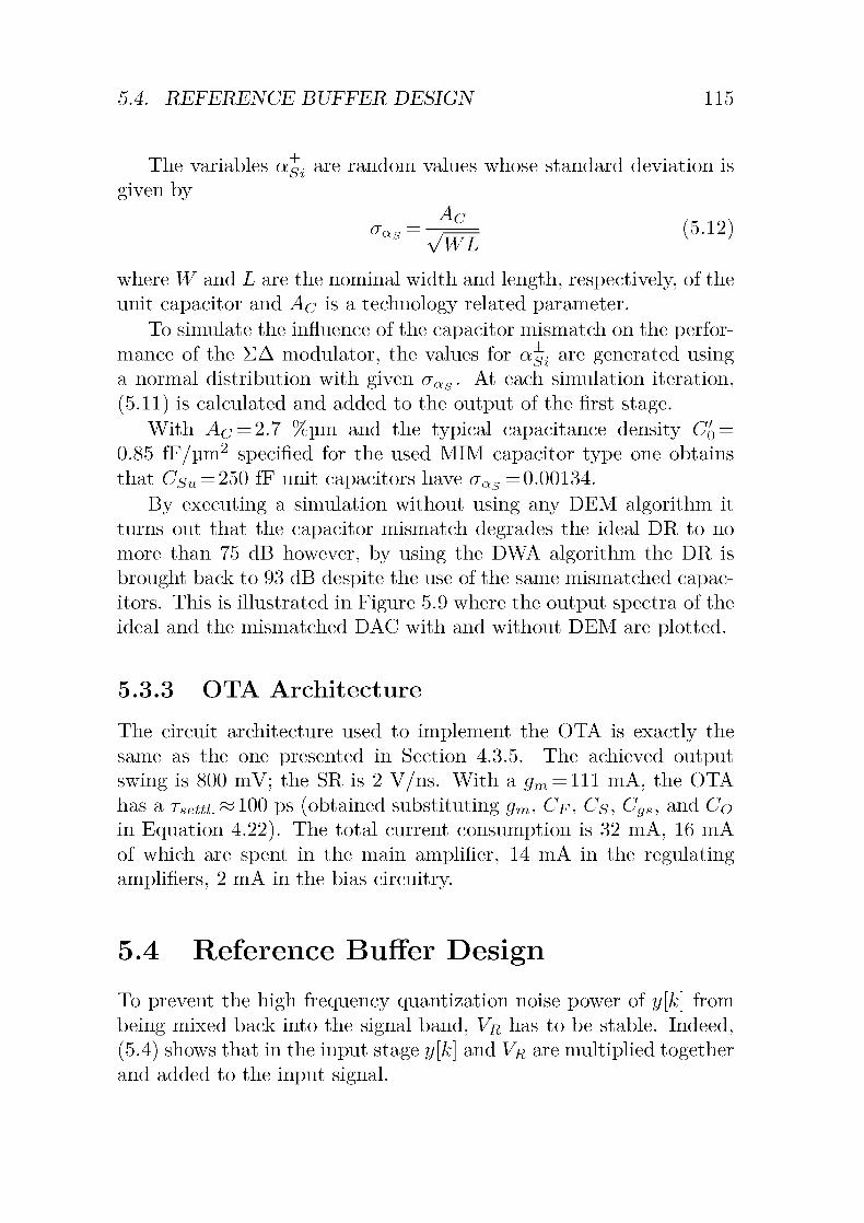
5.4. REFERENCE BUFFER DESIGN 115
The variables aSl are random values whose standard deviation is
given byAr
oas =^=(5.12)
s
VWLV ;
where W and L are the nominal width and length, respectively, of the
unit capacitor and Ac is a technology related parameter.
To simulate the influence of the capacitor mismatch on the perfor¬
mance of the EA modulator, the values for aSt are generated usinga normal distribution with given o~as. At each simulation iteration,
(5.11) is calculated and added to the output of the first stage.
With Ac = 2.7 %mn and the typical capacitance density C'0 =
0.85 fF/mn2 specified for the used MIM capacitor type one obtains
that 6^ = 250 fF unit capacitors have aas =0.00134.
By executing a simulation without using any DEM algorithm it
turns out that the capacitor mismatch degrades the ideal DR to no
more than 75 dB however, by using the DWA algorithm the DR is
brought back to 93 dB despite the use of the same mismatched capac¬
itors. This is illustrated in Figure 5.9 where the output spectra of the
ideal and the mismatched DAC with and without DEM are plotted.
5.3.3 OTA Architecture
The circuit architecture used to implement the OTA is exactly the
same as the one presented in Section 4.3.5. The achieved output
swing is 800 mV; the SR is 2 V/ns. With a 0m = lll mA, the OTA
has a Tseui. ~100 ps (obtained substituting gmi Cf, Cs, Cgs, and Co
in Equation 4.22). The total current consumption is 32 mA, 16 mA
of which are spent in the main amplifier, 14 mA in the regulating
amplifiers, 2 mA in the bias circuitry.
5.4 Reference Buffer Design
To prevent the high frequency quantization noise power of y[k] from
being mixed back into the signal band, Vr has to be stable. Indeed,
(5.4) shows that in the input stage y[k] and Vr are multiplied togetherand added to the input signal.
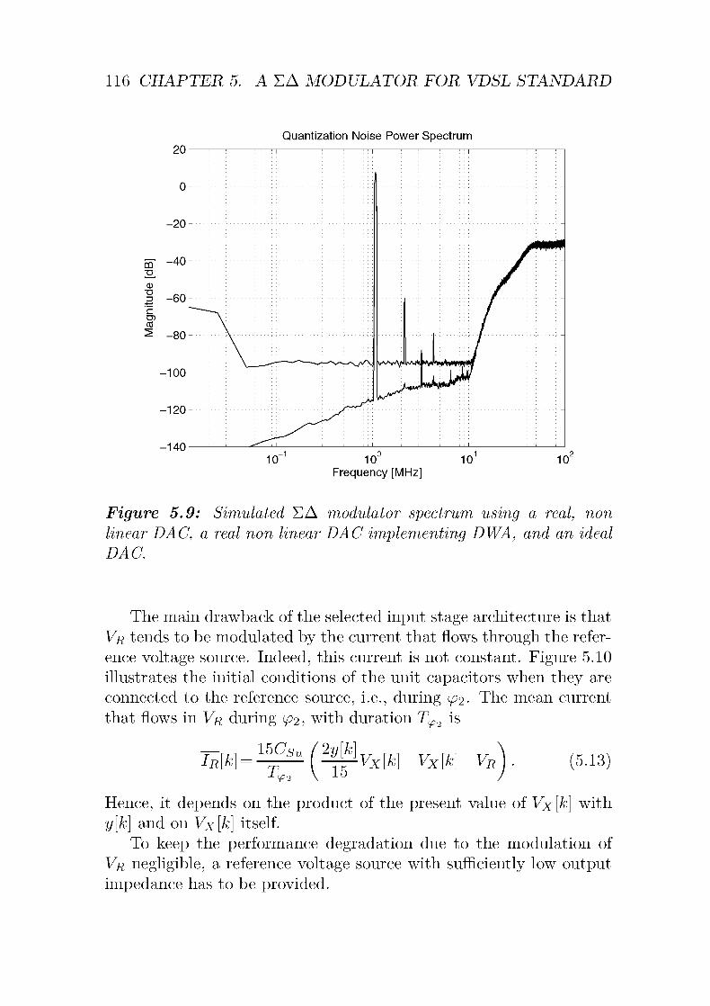
116 CHAPTER 5. A EA MODULATOR FOR VDSL STANDARD
Quantization Noise Power Spectrum
CD
co
20
-20
m-40
-60
-80
-100
-120
-140
10" 10u
Frequency [MHz]
10 10
Figure 5.9: Simulated EA modulator spectrum using a real, non
linear DAC, a real non linear DAC implementing DWA, and an ideal
DAC.
The main drawback of the selected input stage architecture is that
Vr tends to be modulated by the current that flows through the refer¬
ence voltage source. Indeed, this current is not constant. Figure 5.10
illustrates the initial conditions of the unit capacitors when they are
connected to the reference source, i.e., during cf2- The mean current
that flows in Vr during </?2, with duration T(f>2 is
—ril ISCsu (2y[k]IR[k]
liP2 \ 15Vx[k]-Vx[k]-VR (5.13)
Hence, it depends on the product of the present value of Vx [k] with
y[k] and on Vx[k] itself.
To keep the performance degradation due to the modulation of
Vr negligible, a reference voltage source with sufficiently low output
impedance has to be provided.

5.4. REFERENCE BUFFER DESIGN 117
(15-y[k])Csu
y[k]Csu
Figure 5.10: Simplified differential switch level diagram of the input
stage.
5.4.1 Output Impedance Requirements
The requirements for the buffer output impedance are found by be¬
havioral simulation. The used model is explained next. Capacitors
Cx and Cr, and resistors Rx and Rr are resistance and output ca¬
pacitance of the signal and the reference source, respectively. Resistor
Ron is the total switch ON resistance of the sampled unit capacitors
Csu-
During cpi the unit capacitors are connected to the signal source
Vx [k] while the reference source Vr is floating. The resulting single-ended equivalent circuit for cpi is illustrated in Figure 5.11. The initial
conditions of the capacitors depend on the final conditions of the previ¬
ous phase and are V%2[k-1], Vp[k-l], Vp[k-1], and -Vp[k-1],respectively. The latter voltage is the initial condition of the capaci¬
tors previously connected to the Vr negative branch (differential cir¬
cuit). The final voltages V'^1 [/c], V^f1 [/c], and V'^1 [k] are computed at
each clock cycle as a function of the phase duration TVl by solving
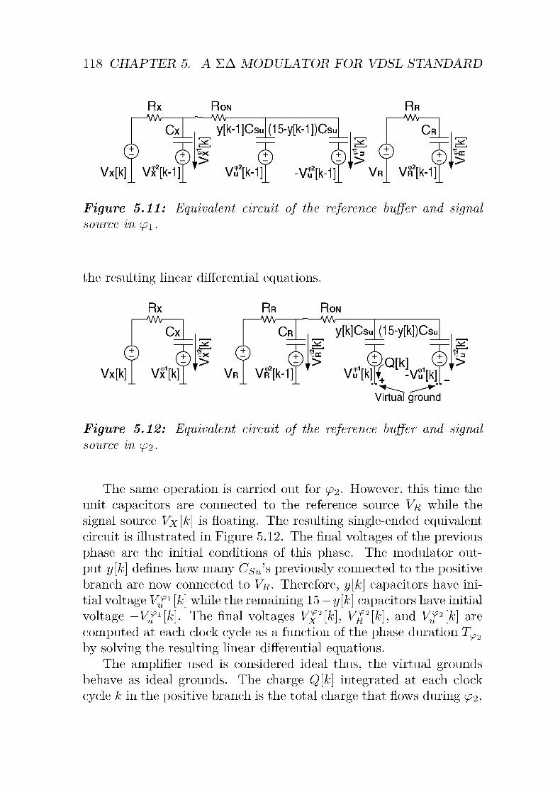
118 CHAPTER 5. A EA MODULATOR FOR VDSL STANDARD
Rx
i—wv-
Cx
Ron-AAAr
Vx[k]1 \/<P.2N, HlT
vr[k-i]
y[k-1]Csu(15-y[k-1])Csu
>,q>2
VuHk-1] VT[k-1]
Rr-A/W-
Cr
^ If? JVr Vff[k-1]
>
Figure 5.11: Equivalent circuit of the reference buffer and signalsource in cpi.
the resulting linear differential equations.
Rx
i—vw-
Cx
Vx[k] W[k]
Rr-AA/V-
Cr
Ron--—vw-
0 m <?>,
$i \/£1ruT T
\/_ \/<£2n, HiTVr Vif[k-1]
y[k]Csu (15-y[k])Csu
Sec
>
VS1[k]?+ -vs1[k]
9-3
>
Virtual ground
Figure 5.12: Equivalent circuit of the reference buffer and signalsource in </?2-
The same operation is carried out for cf2- However, this time the
unit capacitors are connected to the reference source Vr while the
signal source Vx [k] is floating. The resulting single-ended equivalentcircuit is illustrated in Figure 5.12. The final voltages of the previous
phase are the initial conditions of this phase. The modulator out¬
put y[k] defines how many Csu$ previously connected to the positive
branch are now connected to Vr. Therefore, y[k] capacitors have ini¬
tial voltage V^f1 [k] while the remaining 15 — y[k] capacitors have initial
voltage -V^[k}. The final voltages F|2[/c], Vp[k], and V**[k] are
computed at each clock cycle as a function of the phase duration T(f>2by solving the resulting linear differential equations.
The amplifier used is considered ideal thus, the virtual groundsbehave as ideal grounds. The charge Q[k] integrated at each clock
cycle k in the positive branch is the total charge that flows during </?2,

5.4. REFERENCE BUFFER DESIGN 119
from both the positive and the negative (not shown) branch, into the
positive virtual ground
The variation of the single-ended integrator output is
Q[k]
(5.14)
V+[k]-V+[k-l]Cp
(5.15)
The results of the behavioral simulation show that, with Csu =
250 fF, Ron = 30 O, Cx = 5 pF, i?x = 50 O, and CR = b pF, a RR<
10 O is required.
5.4.2 Buffer Architecture
a)
Vi
®"i
M2
/gsMi
Vr—o
Iccomp. _|_
Cl
b) v a
/compJÇc
Vbo-
/gs
—q
Mi Vr-o
IB®
M;
Figure 5.13: Schematic of the reference buffer.
The selected buffer is composed of two separated circuits that gen¬
erate the positive and the negative part of the voltage reference, re¬
spectively; they are shown in Figure 5.13. Since both circuits are
equivalent, only the one for V^T, shown in Figure 5.13-a, is explained.
The buffer has three ranges of operation. At low frequencies, all

120 CHAPTER 5. A EA MODULATOR FOR VDSL STANDARD
c)
lo
-gm2Vl
gmlV2
-O-
Cl /gs
Figure 5.14: Small signal, buffer equivalent circuit at low frequencies
a), at medium frequencies b), and at high frequencies c).
the capacitors are open connections; the equivalent small signal circuit
is depicted in Figure 5.14-a and has the output impedance
1ï'out
9mA 1 +9ml
9o2
(5.16)
i.e., the output impedance l/gmi of Mi is reduced further by the
gain G2=gm2/9o2 of the transistor M2. As the frequency increases,
Rr
-AA/V-
VR,id.(+) Cr: Vr
o-L
Figure 5.15: Equivalent circuit of the reference buffer.
Ccomp begins to conduct; Ccomp can be then assumed to be a short.
The equivalent small signal circuit is depicted in Figure 5.15-b. The
output impedance is
Tout- • (5.17)9rn2
Finally, as the frequency further increases, the output impedance be¬
comes dominated by the capacitors Cgs and Cl connected at the
output node (the equivalent circuit is displayed in Figure 5.15-c). Fig¬ure 5.16 shows the spectral behavior of rout. In this implementation,
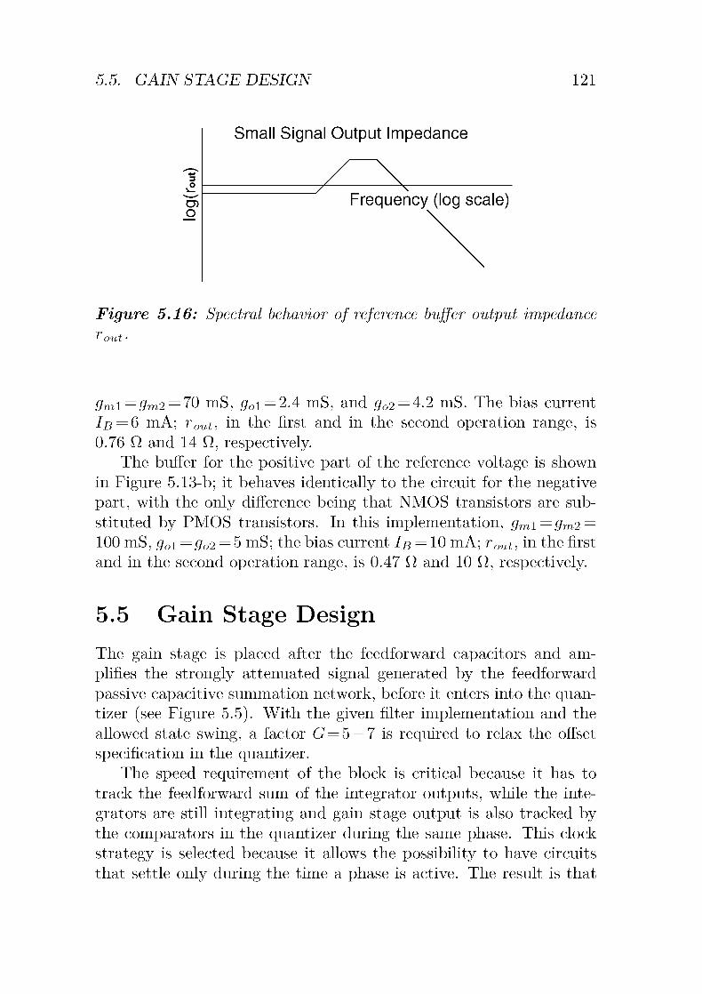
5.5. GAIN STAGE DESIGN 121
o
Small Signal Output Impedance
Frequency (log scale)
Figure 5.16: Spectral behavior of reference buffer output impedanceÏ out
9mi=9m2 = 70 mS, poi = 2.4 mS, and g02 = 4.2 mS. The bias current
Iß = 6 mA; rout, in the first and in the second operation range, is
0.76 0 and 14 O, respectively.The buffer for the positive part of the reference voltage is shown
in Figure 5.13-b; it behaves identically to the circuit for the negative
part, with the only difference being that NMOS transistors are sub¬
stituted by PMOS transistors. In this implementation, gmi=gm2 =
100 mS, g0i=9o2 = ^ mS; the bias current Iß = 10 mA; rout, in the first
and in the second operation range, is 0.47 O and 10 O, respectively.
5.5 Gain Stage Design
The gain stage is placed after the feedforward capacitors and am¬
plifies the strongly attenuated signal generated by the feedforward
passive capacitive summation network, before it enters into the quan¬
tizer (see Figure 5.5). With the given filter implementation and the
allowed state swing, a factor G = 5 —7 is required to relax the offset
specification in the quantizer.The speed requirement of the block is critical because it has to
track the feedforward sum of the integrator outputs, while the inte¬
grators are still integrating and gain stage output is also tracked bythe comparators in the quantizer during the same phase. This clock
strategy is selected because it allows the possibility to have circuits
that settle only during the time a phase is active. The result is that

122 CHAPTER 5. A EA MODULATOR FOR VDSL STANDARD
the time gaps between the phases are minimized and the duration of
</?i and </?2 maximized with the benefit of the integrator blocks.
5.5.1 Linearity Requirements
An open-loop amplifier is selected here to implement the gain stage,
because of its superior speed compared to the classical closed-loopSC block. Open loop amplifiers are known to be inferior in linearityin comparison to the closed-loop counterpart, however, here the gain
stage is placed at the back end of the loopfilter where the sensitivityof the EA modulator to linearity errors is low.
To find the linearity specifications behavioral simulation is againused. A fully differential amplifier usually has its maximum gain Gmax
when the input is around zero and its minimum gain Gmin when the
input is maximum. Furthermore, in fully differential implementationsthe gain function G(x) is symmetric. Because of its simplicity and
because it satisfies the above mentioned requirements the quadratic
expression
G(x)=(\-Gma*-GmmÇ\Gmax (5.18)\ (j'max & J
is selected for G(x)1 where d is the maximum input amplitude. The
G(x)<Umax
Clmin \
/ [ \
i—\—o ru
Figure 5.17: Mathematical model of the variation of the gain G as
a function of the input value x.
proposed curve fits the points at Gmax and Gmin exactly, as is illus¬
trated in Figure 5.17.
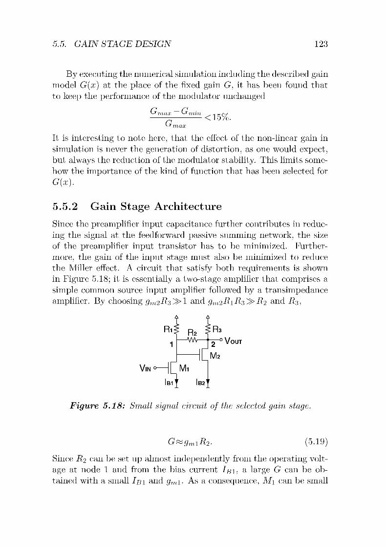
5.5. GAIN STAGE DESIGN 123
By executing the numerical simulation including the described gainmodel G(x) at the place of the fixed gain G, it has been found that
to keep the performance of the modulator unchanged
{J'rn.n.rr. ^mm
„-. - nv
<15%.
^'max
It is interesting to note here, that the effect of the non-linear gain in
simulation is never the generation of distortion, as one would expect,
but always the reduction of the modulator stability. This limits some¬
how the importance of the kind of function that has been selected for
G(x).
5.5.2 Gain Stage Architecture
Since the preamplifier input capacitance further contributes in reduc¬
ing the signal at the feedforward passive summing network, the size
of the preamplifier input transistor has to be minimized. Further¬
more, the gain of the input stage must also be minimized to reduce
the Miller effect. A circuit that satisfy both requirements is shown
in Figure 5.18; it is essentially a two-stage amplifier that comprises a
simple common source input amplifier followed by a transimpedance
amplifier. By choosing gm2-R3^>l and gm2RiR?,^>R2 and A3,
—WV—'^Vout
Vin o
Figure 5.18: Small signal circuit of the selected gain stage.
G^gmlR2- (5.19)
Since R2 can be set up almost independently from the operating volt¬
age at node 1 and from the bias current Ibi, a large G can be ob¬
tained with a small Ibi and gm\. As a consequence, Mi can be small

124 CHAPTER 5. A EA MODULATOR FOR VDSL STANDARD
and the input capacitance can also be small. Furthermore, since the
impedance at node 1 is
under the same conditions given before, Z\ <C-Ri and the Miller effect
is strongly reduced. Not only the impedance at node 1 is reduced but
also the impedance at node 2 indeed,
As a result, the frequency of the poles of the transfer function and the
settling speed are increased.
Due to their excellent temperature independence, unsilicided na¬
tive N+ Polysilicon resistors are used. However, the absolute precisionof these kinds of resistors is poor since the nominal resistance can vary
by ±18% over technology conditions. Furthermore, also the gm of the
employed transistors can vary by ±15% over temperature and technol¬
ogy conditions. As a result, since GttgmlR2, the worst case variation
of G is ±33%. An elegant way to keep G unchanged despite the tech¬
nology variations is to modulate the transistor bias current Iß in such
a way that the product gmR remains constant. Since the gm has a
square root relation with i#, Iß can vary up to ±66%. Thus a largetransistor operating range with respect to Iß is required. The actual,
fully differential, realization of the circuit is shown in Figure 5.19. The
bias currents are defined by transistors Ms and M4; the circuit for the
generation of the regulated voltages Vßni and Vßn2 will be presentedin the next section. The main difficulty in implementing this circuit is
to make it operative over the entire current range. In the straightfor¬ward implementation (black schematic), the operating point voltages
V\ and V2 are exclusively defined by resistors. Thus, by increasingthe bias currents, the voltage drop on R\ and R3 increases linearlywith Iß. Consequently, V\ and V2 are linearly pushed to lower levels.
However, the saturation voltage of transistors Mi, M2, M3, and M4
increases because of the increased Iß. As a result, the transistors stop
very rapidly stop working in the saturation region.
E.g., by increasing I\ and I2 by a factor ß the voltage drop over Ri
is increased by ß and V\ is decreased by the same delta. The source
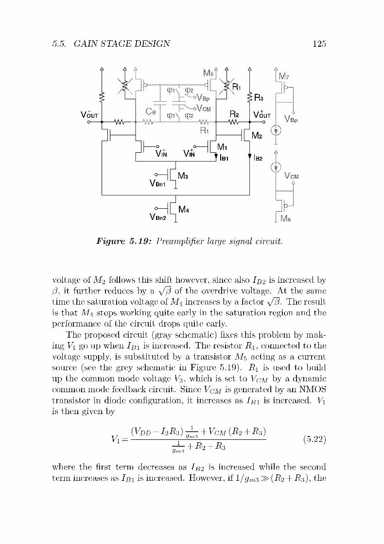
5.5. GAIN STAGE DESIGN 125
VOUT
Mi
Vßn2 \_
M4
f ')y
Vsp
(ï f}Vci
M«
Figure 5.19: Preamplifier large signal circuit.
voltage of M2 follows this shift however, since also Iß2 is increased by
/?, it further reduces by a y/ß of the overdrive voltage. At the same
time the saturation voltage of M4 increases by a factor y/ß. The result
is that M4 stops working quite early in the saturation region and the
performance of the circuit drops quite early.The proposed circuit (gray schematic) fixes this problem by mak¬
ing V\ go up when Ibi is increased. The resistor i?i, connected to the
voltage supply, is substituted by a transistor M5 acting as a current
source (see the grey schematic in Figure 5.19). R\ is used to build
up the common mode voltage V3, which is set to Vqm by a dynamiccommon mode feedback circuit. Since Vqm is generated by an NMOS
transistor in diode configuration, it increases as Ibi is increased. V\
is then given by
(VDD-l2R3)y-+VCM(R2+R3)17
' 9m3 v '
9m3+ R2+R2
(5.22)
where the first term decreases as Ib2 is increased while the second
term increases as Ibi is increased. However, if l/gm3 ^> (R2 + R3), the
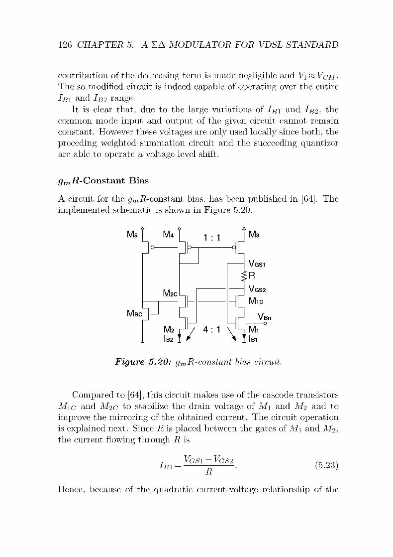
126 CHAPTER 5. A EA MODULATOR FOR VDSL STANDARD
contribution of the decreasing term is made negligible and V\^Vcm-
The so modified circuit is indeed capable of operating over the entire
Ibi and Ib2 range.
It is clear that, due to the large variations of Ibi and Iß2, the
common mode input and output of the given circuit cannot remain
constant. However these voltages are only used locally since both, the
preceding weighted summation circuit and the succeeding quantizer
are able to operate a voltage level shift.
grm.R-Constant Bias
A circuit for the gm.R-constant bias, has been published in [64]. The
implemented schematic is shown in Figure 5.20.
Figure 5.20: gmR-constant bias circuit.
Compared to [64], this circuit makes use of the cascode transistors
Mic and M2C to stabilize the drain voltage of Mi and M2 and to
improve the mirroring of the obtained current. The circuit operationis explained next. Since R is placed between the gates of Mi and M2,the current flowing through R is
ImVgsi — Vgs2
R(5.23)
Hence, because of the quadratic current-voltage relationship of the
5.5. GAIN STAGE DESIGN 127
MOS transistor, one obtains
Vgsi-Vt = — (5.24)9ml
Vgs2-Vt = —- (5.25)9m2
Since M3 and M4 are identical, Ibi = Ib2 = Ib- Thus, by substituting
Equations (5.24) and (5.25) in Equation (5.23) one finds that
R. (5.26)9ml 9m2
Finally, by setting grn2 = ^9mi and W2 = AW\, Equation (5.26) be¬
comes
^- = R. (5.27)9ml
Equation (5.27) shows that the implemented circuit generates an Iß
that keeps gm\R=\1 independently of what the absolute gm\ and R
are.
The presented circuit works as long as the simple quadratic model
of the MOS transistor is valid. Due to the low supply voltage of the
technology used, to give more range to the further stacked transistors
one is forced to minimize the saturation voltage of Mi (replica of Mi
are used as current sources). Thus, Mi has to work near to the mod¬
erate inversion; then, since M2 is biased by the same current as Mi
but has W2 = AW\, it is very likely not to operate in strong inversion.
As a result, the current-voltage relation of M2 is not quadratic and
the obtained gmR is not exactly constant. Nevertheless, simulations
have shown that the gain variation is sufficiently small for the purpose
required.
The entire preamplifier with the gm.R-constant bias is simulated
in typical, best, and worst case conditions. Typical case means, here,T=27 C, typical technology speed and nominal resistor value; best
case means T=0 C, fast technology and maximum resistor value; fi¬
nally, worst case means T=70 C, slow technology and minimum resis¬
tor value.

128 CHAPTER 5. A EA MODULATOR FOR VDSL STANDARD
In typical conditions Gmax = 6.9, Gmm = 6.87 for an input swingof 100 mV, /3dB = 2.03 GHz by a load of 500 fF, and the total current
consumption is Itot = 9.5 mA; in best conditions Gmax = 7.2, Gmin = 7,
/3dB = l-77 GHz, and the total current consumption is 7ioi = 6.0 mA;
finally, in worst conditions Gmax = 5.98, Gmin = 5.95, /3dB = 2.38 GHz,and the total current consumption is Itot = 17.6 mA. These results
show that Gmax is still quite constant over the worst-, typical-, and
best-case conditions while the variation of G, over the input swingof 100 mV, is for all conditions better than 5%; it is therefore much
better than specified.
Since, in worst and in best case conditions, the resistor values are
minimum and maximum, respectively, /3dB is maximum for the worst
case conditions and minimum for the best case conditions. The input
capacitance is 70 fF.
5.6 Quantizer Design
The quantizer is placed after the gain stage and it converts the analog
loopfilter output into a 4 bit digital value. This value represent the
output of the EA modulator and the input of the internal DAC (seeFigure 5.5).
The architecture chosen for the quantizer is fully differential and
is illustrated in Figure 5.21 for n = 2. A resistor chain with identical
unit resistors Ru builds up the voltage references that are sampled on
capacitors Cq's during cpi and added to the loopfilter output voltage
Vyh during cp2- The resulting signal is then sensed by the comparators
that are regenerated at the end of (f2-
The following sections will show how the requirements of each
block composing the quantizer are found and how the requirements
are mapped to the specifications of the actual circuit realizations.
The trade-offs in design of the selected analog building blocks will be
illustrated as well.
5.6.1 Uniformity Requirement
The main specification for the quantizer used in this EA modulator
is its uniformity. In fact, despite a small n (4 bit), the accuracy of

5.6. QUANTIZER DESIGN 129
Figure 5.21: Simplified, for n = 2, Switch level diagram of the im¬
plemented quantizer.
the quantizer uniformity needs to be much higher than n. Behavioral
simulation is used to determine the uniformity requirements.
To carry out the reduction of the quantizer uniformity, the dis¬
tances between the reference levels are randomly shifted using a nor¬
mal distribution with standard deviation gq. By simulating the mod¬
ulator with the quantizer which is obtained, what happens is that the
loop performance is not worsened as long as <7q<0.5% of the con¬
version range. With a gain stage G = 6 (Section 5.5) the quantizer
differential input signal swing is 1.2 V, hence gq <6 mV. This specifi¬cation can be directly referred to the specification of the comparator
input offset. Nevertheless, the comparators are not the only source of
uniformity degradation in the quantizer with the selected architecture.
These will be discussed in the following sections.

130 CHAPTER 5. A EA MODULATOR FOR VDSL STANDARD
5.6.2 Capacitor Matching Requirement
Cq
92/.
VcmG+VcS2
cpi\Si
ComparatorvSo—
<P1
Vqo
.o o
VcmREF+VREFi Vcmin
Cgigs
Figure 5.22: Switch level diagram of the circuit for implementingthe differential difference.
Figure 5.22 shows the single-ended switch level diagram of a com¬
parator. Where, VcrnG, VcrnREF, and Vcrnin are the gain stage, ref¬
erence resistor ladder, and comparator common modes, respectivelyand C+, is the parasitic gate capacitance of the comparator inputtransistor.
The value of VÂ at the beginning of the comparator regenerationtime (end of ^2) is
VA = (Vcm G Vc,+
cmREF,
Cq ± CgS~r Vcmzn-\-yvq V-,
REFi
c,+
Cn ±CQgs
(5.28)The value of Vq is given by the same equation where Vq and V^EFlare substituted by Vq and VR~EFï, respectively and where the CX and
C+, are substituted by Cq and C~s.
As long as Cq=Cq and C^S = C~S, setting Vq = Vrff% leads to
however if, e.g., CX = Cq ± ACq an imbalance is generated and VÂ^0. This is the source of uniformity degradation due to the capacitormismatch. Assuming that ACq<C1, one finds that the imbalance is
Vd
?e|ACQ/0
, dV+(C+)v++ Q:.Q ACc
dC,+
v; (5.29)VG=VREFt

5.6. QUANTIZER DESIGN 131
where Vq(CX) is linearized with respect to CX. Solving (5.29) gives
\rd I —(V 1/ \ CgsCQ ACq
VUc^„-(^G-^w)(c^ +C(3)2—•(5.30)
The interesting information in (5.30) is that the mismatch of Cq does
not have any influence on the uniformity of the quantizer as long as
VCrnG = VcmREF- By making VcmREF externally adjustable in this de¬
sign, the influence of the mismatch of capacitor Cq on the modulator
performance can be made negligible. This is in fact also true for Cgs
VQe\AC^0 = (VcmG-VcmREF)9* Q
^"TT^- (5'31)9 ^ (Cgs+CQ) ^gs
5.6.3 Switch Requirements
The switches can contribute to the degradation of the quantizer uni¬
formity in two ways. The first way is by injecting a charge that de¬
pends on the signal they are connected with. The second way is by a
mismatch of the injected charges due to the mismatch of the switches
themselves. Both effects are joined together under the concept of clock
feedthrough [65].Figure 5.22 shows the position of the three switches involved in the
quantizing operation (single-ended schematic). The subscript symbolD in the phase name means that the signal is delayed. This circuit is
repeated 15 times with only a change of the voltage Vref%-
During cpi_, the voltage on Cj is set to Vref% (VCmREF = Vcm%n).Switches S\ and S3 are closed while S2 is opened. At the end of </?i,
S3 opens first, injecting some charge on CX. Since S3 is connected to
a voltage that is the same in each comparator the clock feedthrough
depends only on the matching of S3. Then Si also opens but since S3
is already opened, the charge injected by Si generates only a chargeredistribution and it is not sampled on CX. After the end of tp\1 CX
is connected to the quantizer input signal CcrnG + VQ by closing S2.
The voltage previously sampled on CX is then subtracted from the
input and passed to the comparator. The comparator tracks its input
during the entire </?2 and is latched at the end of the phase. After a
while also S2 is closed and some charge is injected. However, since

132 CHAPTER 5. A EA MODULATOR FOR VDSL STANDARD
the comparator has been previously latched this charge has no effect
on the decision.
In conclusion, it can be observed that the only switch that can
generate clock feedthrough and reduce the quantizer uniformity is S3.
Thus only switch S3 requires some care during the layout phase. It is
interesting to note that in the circuit shown in Figure 5.22 there is no
clock feedthrough due to signal dependent charge injection.
5.6.4 Resistor Ladder Design
The resistor ladder is composed of 16 identical resistors that generate
at the internal nodes a uniform sequence of 15 reference voltages.
Resistor Matching Requirement
The first condition, for having a perfectly uniform sequence of ref¬
erence voltages, is to have unit resistors that match perfectly. The
equation that relates the matching parameter of the unit resistance
0"Afl„ to the relative standard deviation of the random variation of
the reference voltage gavref has been given in [3] and is
(JAVREF=
1 (JARU(5^2)
Vladder \[ÄM Ru
where M and Viadder are the length and the external differential volt¬
age of the resistor ladder, respectively.With M=16 and VRzac^er = 600 mV of this design, one obtains
that to achieve gq<6 mV, garu/Ru<^%. This matching specifica¬tion is very relaxed and can even be easily outperformed.
Ladder Bowing Requirement
A bowing of the reference sequence is generated when current is flow¬
ing away from any of the internal nodes of the ladder. This is the
case for the SC quantizer architecture used here. Indeed, a chargeis transfered from every node of the resistor ladder to the sampling
capacitor Cq during each clock cycle.To analyze this problem, a node of the resistor ladder, shown in
Figure 5.23 with its loading circuitry, is studied; Ca is the parasitic

5.6. QUANTIZER DESIGN 133
VcmREF+VREFi
VcmG+VÖ 9 Ru J / 9 VcmG+Vc
Figure 5.23: Circuitry connected to one node of the resistor ladder.
capacitance at the side of Cq, connected to the reference voltage.Since the resistor ladder is used in a fully differential quantizer, the
node is connected to a positive (on the right) and to a negative (on the
left) branch, respectively of two different comparators. To find out the
current flowing out from the resistor ladder, the delivered charge Q^and Q~ is calculated and added together. The resulting total chargeis
Qi = QÏ + Q7 = (2VREFï)(CA + CQ\\Cgs) (5.33)
and the mean current flowing out from the node is
Iref
R
Vref
eq
(CA+CQ\\Cgs) fs
(5.34)
(5.35)
where Req is the SC equivalent resistance.
Equations (5.34) and (5.35) are used to calculate the bowing of
the resistor ladder. The resistor ladder with the equivalent resistive
loads is shown in Figure 5.24.
With CQ=300 fF, CA = 20 fF, Cgs = 28 fF, and /s = 200 MHz the
equivalent resistor is Req = bb kO. Simulation executed with the mod¬
ified reference levels have shown that for a proper operation of the
EA modulator Ru has to be less than 250 O.
The above results give a minimum requirement for the resistor

134 CHAPTER 5. A EA MODULATOR FOR VDSL STANDARD
Vtadder Ruo—vvv-
Ru-AAAr
Ru-AAAr
Ru Vladder
-AAA o
iReq:R
eq:R
eq iReq
Figure 5.24: Resistor ladder with equivalent resistive loads.
ladder. However, during each phase the ladder is also subjected to
strong current pulses generated by the switches. Hence the internal
nodes have to be sufficiently fast to absorb these pulses in the time of
a single phase.The most critical node is the one in the center of the resistor ladder
because it sees the highest impedance. The most critical phase is cpi
because Cq is connected to the node and the capacitive load is higher.
Analog simulations have shown that, to achieve a maximum shift of
the reference voltage of 1 mV, Ru = 2b Q is needed.
5.6.5 Comparator Architecture
Figure 5.25: Circuit schematic of the implemented comparator.
The comparator used in this design is depicted in Figure 5.25. The
operation of this circuit is very similar to the operation of the circuit

5.6. QUANTIZER DESIGN 135
described in Section 4.4.1. The voltage Vab tracks Vq during cp2
while, for the rest of the time, the initial Vab imbalance is regenerated.To prevent the succeeding digital logic taking an initial wrong decision,the two NAND gates, introduce a small delay between the beginningof the regeneration phase (end of cpi) and the instant where the output
of the comparator is made transparent (begin of ^2). The SR latch
keeps the last output state when the comparator is reset.
Compared to the comparator presented in Section 4.4.1, this cir¬
cuit has a faster tracking mode since the upper, slow, PMOS current
mirrors are substituted by a folded cascode structure. The comparator
must be fast because it is chained to the integrators and the pream¬
plifier and must settle together. The poles of the circuit, in tracking
mode, are
9m2 fr. oß\Pi =
-ç- (5-36)
1 2-rONP2 =
-fi , (5.37)^2 ton
where C\ and C2 are the total capacitive load of node 1 and 2, respec¬
tively and roN is the ON resistance of the switch transistor Mq. In this
design, the dominant pole is pi; with Ci = 62 fF and gm2 = 0.75 mS,
fPl =1.91 GHz. Transistor Mo receives a bootstrapped clock signal to
keep Wq and consequently C2 small. Figure 5.7 illustrates the used
charge pump circuit.
The offset of the comparator has a direct influence on the unifor¬
mity of the quantizer. The equation for the calculation of the standard
deviation of the drain current of two identical matched transistors is
<rAJ = -^=WPV
. ±J) +Ä* (5.38)
where, gm and Vas are the nominal transconductance and the gate-
source voltage, W and L are the channel width and length, and Aßand AyT are technology related parameters for the transconductance
and the threshold voltage mismatch, respectively. Since Aß<^AyTand since (Vos — Vt)<^1, the first term under the root of Equation
(5.38) can be neglected, furthermore, since gavgs =(JAi/g?imi
Av,
aAVas=vwz' (5'39)

136 CHAPTER 5. A EA MODULATOR FOR VDSL STANDARD
By assuming that the NMOS and PMOS transistors have similar AyT,the total influence of the <7avGs °f each couple of transistors, referred
to the input of the comparator, is
—Af(ä2+2!(ä2 ^
where L3 and L4 are the lengths of M3 and M4, and K,'n and k'p are the
transconductance parameters of the NMOS and PMOS transistors,
respectively.To minimize <jaVbs5 -^3 an(^ -^4 are set greater than Li. In this
design, the transistors of the comparator are dimensioned to achieve
o"AVos=3-4 mV.
5.7 Data Weighted Averaging Algorithm
Design
The data weighted averaging (DWA) algorithm is used to select the
unit elements of the DAC in such a way that the linearity error due
to the capacitor mismatch is modulated at frequencies outside the
signal band. The DWA is placed between the quantizer and the input
DAC. It consists of the DEM block and the logarithmic shifter (seeFigure 4.8).
The DWA algorithm requires that the unit capacitors of the DAC
are employed, as if they were elements of a circular buffer. To imple¬ment the current DAC value, one has to utilize the first element of the
buffer that has not yet been used in the previous value and to sequen¬
tially take as many units as defined by the digital input. The buffer
must always be walked through in the same direction. Figure 5.26
illustrates the operation of the selection of the unit capacitances for a
circular buffer of length 15 and a digital partial sequence y[k]=b and
y[k + l] = 12.
5.7.1 Algorithm Implementation
Figure 5.27 shows the main blocks of the DWA logic. A first block
counts the number of l's present in the quantizer thermometer coded

5.7. DATA WEIGHTED AVERAGING ALGORITHM DESIGN137
y[k]=5
y[k+1]=12
Figure 5.26: DWA algorithm working principle.
Q[k]
'15
1'S
counter
A[k]
RegState[0..3]
92
Modulo
15 adder
RegOut[0..3]
y[k]
t (p2
Figure 5.21: Block Diagram of the DWA logic.
output (a true ones-counter is used, here, to deal with code bub¬
bles). The sum is passed to the output register RegOut and to the
modulo-15 adder that adds it to the current control signal of the log¬arithmic shifter, stored in the register RegState; the result is passedto RegState. At the </?2 falling edge then, both registers, RegOut and
RegState, fetch their input data and the number of ones will be the
current output value of the EA modulator, while the result of the

138 CHAPTER 5. A EA MODULATOR FOR VDSL STANDARD
modulo-15 sum will be the current control signal of the logarithmicshifter.
The implemented DWA logic has a delay of less than 4 ns and
utilizes 94 digital standard cells.
5.7.2 Logarithmic Shifter Architecture
The implemented circuit maps Xq. .. X\^ inputs to Yq ... Y\± outputs.
The four bit wide A^... A3 controlling signal defines the spatial shift
of each output compared to the corresponding input.
Figure 5.28: Single Slice of the logarithmic shifter circuit schematic.
The structure of the logarithmic shifter is very repetitive; one of
the 15 used identical slices is depicted in Figure 5.28. The slices are
aligned one close to the other. The dashed connections are connections
between external slices. The remaining connections, of the first and
of the last slice, have to be made manually pretending that the two
slices are near to the other.
The internal branches are implemented by couples of NMOS tran¬
sistors toggled by inverted signals (Ai and Ai). Since NMOS tran¬
sistors can only raise the signal up to Vdd—Vt, level restorers are
used. Two level restorers limit the number of series connected NMOS
switches to two.

5.8. EXPERIMENTAL RESULTS 139
5.8 Experimental Results
The EA modulator is implemented in a digital triple well 0.18 pm
CMOS process with seven metal layers (one of them is a tungsten
layer for local interconnections, only), one polysilicon layer, and the
option for MIM capacitors. The power supply is 1.8 V.
Figure 5.29: Chip photomicrograph of the EA modulator.
The chip photograph is depicted in Figure 5.29. The big vertical
stripe at the furthest left position is the reference buffer (1); it con¬
sists mainly of decoupling unit capacitors, made by PMOS and NMOS
transistors of lOxlOmn area, and of the actual circuit that is situated
in the middle of the stripe. The input stage (2) is at the right side
of the reference buffer; it occupies 3/5 of the core width. From the
bottom to the top, one can distinguish the OTA, composed of eightunit OTAs and separated by two supply vertical stripes, the associ¬
ated MIM capacitors, the switches, crossed by the horizontal clock
bus, and the capacitors of the charge pump. The bias circuitry of the
OTAs and some decoupling MOS capacitors (3) are at the right of

140 CHAPTER 5. A EA MODULATOR FOR VDSL STANDARD
the input stage; above them, the MIM capacitors and the associated
switches of the FF path can be identified. By moving further towards
the upper part of the circuit, one can distinguish the square shaped
preamplifier (4). The remaining stages (5) of the loopfilter are next
to the bias circuitry. From the bottom to the top, one can distinguishthe OTAs, separated by power supply vertical stripes and the respec¬
tive MIM capacitors with the associated switches. The 4 bit quantizer
(6) is placed above the switches; it consists of 15 thin identical ver¬
tical stripes containing a charge pump, two sampling capacitors, and
a comparator. The logarithmic shifter and the DWA logic are placedat the upper end of the quantizer. The circuit order in the quantizeris from the "most analog" (bottom part) to the "most digital" (upperpart). The resistor ladder network uses the entire width of the quan¬
tizer but it cannot be seen, since it is under the sampling capacitors.
The digital circuit for the generation of clock phases (7) is at the rightend of the clock bus. The entire core occupies an area of 0.95 mm2.
To reduce the noise coupling, the reference buffer, the integrators,the preamplifier and the analog part of the quantizer, the digital part
of the quantizer, the buffers of the digital pads, and the remaining
digital logic have a separated power supply. Analog and digital padsare further isolated from each other, by using separated pad rings.The output pad buffers are differential with constant bias currents;
Off Chip
X] Kl PADS
Figure 5.30: Differential digital output buffer.
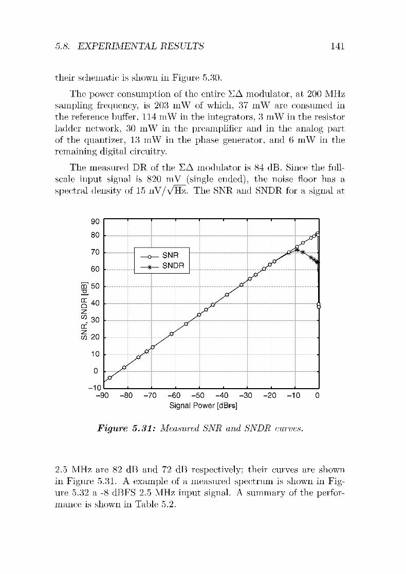
5.8. EXPERIMENTAL RESULTS 141
their schematic is shown in Figure 5.30.
The power consumption of the entire EA modulator, at 200 MHz
sampling frequency, is 203 mW of which, 37 mW are consumed in
the reference buffer, 114 mW in the integrators, 3 mW in the resistor
ladder network, 30 mW in the preamplifier and in the analog part
of the quantizer, 13 mW in the phase generator, and 6 mW in the
remaining digital circuitry.
The measured DR of the EA modulator is 84 dB. Since the full-
scale input signal is 820 mV (single ended), the noise floor has a
spectral density of 15 nV/vHz. The SNR and SNDR for a signal at
90
80
70
60
m 50
| 40
^30cc
OT 20
10
0
-10
-90 -80 -70 -60 -50 -40 -30 -20 -10 0
Signal Power [cIBfs]
Figure 5.31: Measured SNR and SNDR curves.
2.5 MHz are 82 dB and 72 dB respectively; their curves are shown
in Figure 5.31. A example of a measured spectrum is shown in Fig¬ure 5.32 a -8 dBFS 2.5 MHz input signal. A summary of the perfor¬
mance is shown in Table 5.2.
t 1 1 1 1 r
J i I i i i i L

142 CHAPTER 5. A EA MODULATOR FOR VDSL STANDARD
0.001 0.01 0.1 1
Frequency [MHz]
4 6 8
Frequency [MHz]
10 100
Figure 5.32: Full and close-in view of the measured spectrum.
DR
Peak SNR
Peak SNDR
Input Range
84 dB
82 dB
72 dB
1.6 Xpp diff.
ÎB
fsOSR
10.6 MHz
200 MHz
8
Power SupplyPower Consumption
1.8 V
203 mW
Process
Core Area
CMOS 0.18um lp7m0.77 mm2
Table 5.2: Characteristics of the EA modulator.
5.9 Summary
The design of a 25 MS/s, 14 bit EA modulator with 8x OSR and
implemented in a digital 0.18 urn technology has been described in

5.9. SUMMARY 143
this chapter.The modulator employs a 5* order loopfilter with two internal
feedback loops and a 4 bit quantizer. The peak SQNR of the imple¬mented loopfilter is 96 dB.
The circuit implementation is SC. An input stage architecture with
single capacitor for signal and voltage reference is used. The effects of
the signal and feedback dependent current sinked from the reference
voltage, by the input stage, are carefully analyzed. To keep the output
impedance of the voltage reference low, an active buffer is designed.Due to the low supply voltage (1.8 V), the speed of the switches
was a problem in this design; charge pumps are used where neces¬
sary. Since the weighted sum of the feedforward paths is implemented
by capacitor charge sharing, an open-loop amplifying stage is put in
front of the 4 bit quantizer to amplify the resulting attenuated signal.The effects of the amplifier linearity are studied in simulation usinga quadratic model. To keep the gain of the amplifier constant, over
technology speed and temperature variations, a special gmR-constant
bias is employed. The 4 bit quantizer makes the required difference
of differential signals using an SC circuit. The reference levels are
generated from a resistor ladder network. The selected comparator
combines the speed of the folded-cascode amplifier, during the track¬
ing phase, with the speed of the NMOS latch, during the regenerating
phase. The effect of each non-ideality such as resistor, capacitor, and
transistor mismatch, on the uniformity degradation of the quantizer,is analyzed. The feedback DAC uses 15 unit capacitors to implementthe required 16 levels, to linearize the DAC a DWA algorithm is cho¬
sen. The clock phasing arrangement reserves a complete clock periodfor the logic operations related to the DWA algorithm.
The measured DR of the implemented EA modulator is 84 dB, its
power consumption is 203 mW. Figure 5.33 shows how the achieved
bandwidth/resolution pair compares to the results obtained by other
recently published EA modulators. As can be observed, no other
modulator can achieve such a high DR in this order of conversion
bandwidth.

144 CHAPTER 5. A EA MODULATOR FOR VDSL STANDARD
100 -
„ 90
8)80c
CO
rr
o 70ECO
§60
50
I '
^'(6)"X
-
- (1)X
X(4)X(5)
This
Work"
X
~ (2)X
(3)-
X (8) -
(7)X
X
....i . .
100k 1M 10M
Signal Bandwidth [Hz]
Figure 5.33: Comparison of the current modulator resolution and
bandwidth. (l)-[66], (2)-[68j, (3)-[30j, (4)-[25j, (5)-[61], (6)-[56],(1)-[69J, (8)-[10[.

Chapter 6
Conclusions
The increasing demand for broadband Internet access and the growinguse of digital processing, motivates the implementation of communica¬
tions standards employing sophisticated decoding methods, capable of
achieving high data rates using existing communications media. How¬
ever, the trend toward increased data rates and digital signal process¬
ing increases the dynamic range (DR) and the bandwidth needed at
the A/D interface.
Sigma-Delta (EA) ADCs have tolerance for component mismatch
and circuit non-idealities. Furthermore, EA ADCs simplify system
integration by reducing the burden on the supporting analog circuitry.
Specifically, they do not require precision S/H circuitry and they relax
the specifications of the anti-aliasing filter. Even the synchronizationof the transmitted symbols is simplified when EA ADCs are used
because of the oversampled signal.
Oversampling is however the main weakness of EA modulators
since it prevents high conversion rates from being achieved. Several
attempts [52] [30] [56] have been made to increase the conversion
rate by minimizing the oversampling ratio but they have somehow
overlooked another important aspect i.e., the maximization of the
sampling frequency. In this thesis both aspects have instead been
considered.
Since the specifications of the analog building blocks are deter-
145

146 CHAPTER 6. CONCLUSIONS
mined by the architecture of the EA modulator, the choice of an
architecture that puts low speed specifications on the analog buildingblocks despite high sampling rates constitutes a central point in this
work. Furthermore, sufficient DR at low OSR has to be provided, as
well.
Because the discrete-time EA modulator has lower clock jitter
sensitivity than its continuous-time counterpart, it relaxes the clock
circuit specifications at high sampling frequencies. Therefore, the
discrete-time architecture is selected in this work. The single-looparchitecture is better suited for the implementation of broadband EA
ADCs than the cascaded architecture because it puts lower amplifierDC gain specifications. High DC gains are difficult to obtain using fast
CMOS technologies required for achieving high sampling rates. The
feedforward is preferred to the feedback loopfilter topology because
it has larger input coefficients that better attenuate the influence of
the internal node disturbances. This is advantageous in low OSR EA
modulators, where the gain of the integrator at the edge of the signalband is low. Finally, high DR at low OSR are obtained using a multi-
bit architecture. The dynamic element matching method is preferredto laser trimming and digital correction for the DAC linearization
because of its simplicity and because it also corrects dynamic errors
(temperature variation, component aging, etc.).The influence of the DAC nonlinearity on the overall performance
is further analyzed. A method to calculate the performance degrada¬tion due to the trilevel DAC non-ideal characteristic is proposed.
The method employs three simplifications: the influence of the
DAC linearity error in the EA loop is considered negligible comparedto the influence of the quantization error; the quantizer is substituted
by a sum of an uncorrelated, white, uniformly distributed noise; the
DAC characteristic function is interpolated by a second order polyno¬mial function.
A closed equation for calculating the power spectrum of the EA
modulator output signal is given. The equation is analytically solved
for the practical case of a 5th order modulator with 1.5 bit quantizer.The maximum error achieved in the calculation of the signal-to-noiseratio curve remains always below 7 dB. Calculation results show that
the DAC linearity has a strong influence on the overall ADC perfor¬
mance.

147
The remaining part of the thesis is dedicated to the description of
two designs namely, a EA modulator for ADSL standard and a EA
modulator for VDSL standard. Both use an architecture whose main
features have been previously outlined.
The design of the ADSL modulator with a 2.5 MS/s, 14 bit EA
modulator, and 32x OSR is described first. The modulator employs a
bth order loopfilter with two internal feedback loops and a 1.5 bit quan¬
tizer. To reduce the power consumption, the desired DR is achieved
using the smallest possible capacitance area. To achieve the speci¬fied resolution the effects of the circuit non idealities on the linearityof the selected DAC architecture are calculated. A simple flow for
determining the required OTA GBW and SR, as a function of sam¬
pling frequency and final resolution is then proposed. The switches
are dimensioned for maximum settling speed. The EA modulator is
implemented in a 0.25 urn technology. The measured DR, peak SNR
and peak SNDR are 89 dB, 85 dB, and 79 dB respectively and corre¬
spond quite well to the designed values. The total power consumption
is 24 mW which was, at the time the circuit has been published, the
lowest power consumption achieved by a EA modulator with this or¬
der of resolution/bandwidth.The good measurement results of the ADSL EA modulator allowed
us to go one step further in the development namely, to increase the
conversion speed. The design of the VDSL modulator with a 25 MS/s,14 bit EA modulator, and 8x oversampling-ratio is described. The
modulator employs a 5th order loopfilter with two internal feedback
loops and a 4 bit quantizer.An input stage architecture with single capacitor for signal and
voltage reference is selected to reduce the capacitor area. The effects
of the signal and feedback dependent current sinked from the reference
voltage are carefully analyzed. A fast buffer, used to keep the output
impedance of the voltage reference low, is designed. Charge pumps
are used where the speed of standard MOS switches are not enough.Since the weighted sum of the feedforward paths is implemented
by capacitor charge sharing, an amplifying stage is required in front
of the quantizer, to amplify the resulting attenuated signal. Due to
its superior speed, an open-loop amplifier is selected. The amplifier
gain linearity constraints are obtained by means of behavioral simula¬
tions and using a quadratic model. To keep the gain of the amplifier

148 CHAPTER 6. CONCLUSIONS
constant, over technology speed and temperature variations, a special
gmR-constant bias is employed.
The quantizer makes the required difference of differential signals
using an SC circuit. The 15 reference levels are generated from a re¬
sistor ladder network. The selected comparator combines the speedof the folded-cascode amplifier, during the tracking phase, with the
speed of the NMOS latch, during the regenerating phase. The spec¬
ifications of the analog building blocks composing the quantizer are
determined by behavioral simulation.
The feedback DAC uses 15 unit capacitors to implement the re¬
quired 16 levels, to linearize the DAC, a data weighted averaging
algorithm is chosen. The clock phasing arrangement reserves a com¬
plete clock period for the logic operations related to the data weighted
averaging algorithm.
The EA modulator is implemented using a 0.18 urn CMOS tech¬
nology with one layer of polysilicon, six layers of metals, and option
for MIM capacitors. The measured DR at 25 MS/s conversion rate
is 84 dB which corresponds to a resolution of 14 bit. The power
consumption is 203 mW. This modulator outperforms in speed any
previously published 14 bit (effective number of bits) EA modulator.
In this thesis it has been demonstrated that, by using fast CMOS
technologies and by selecting the right EA modulator and circuit ar¬
chitectures, ADCs with conversion rates up to several tens of MS/sand 14 bit resolution can be implemented. This kind of performancehas been obtained only by Nyquist converters, so far. However, Ny¬
quist converters have several disadvantages and suffer from the reduc¬
tion of signal swing in deep sub-micron CMOS technologies while EA
ADCs do not.
One possible problem of the chosen EA ADC architecture, with
respect to its implementation in deeper sub-micron CMOS technolo¬
gies, is the degradation of the switch speed due to the reduction of
the overdrive voltages. A solution to this problem has been partially
presented in Chapter 5 where charge pumps have been employed to
decrease the switch resistance at the modulator input node. It is very
likely that, to take advantage of the faster transistors, charge pumps
have to be implemented for other switches, as well when CMOS tech-

149
nologies with even smaller channel lengths are taken. However, the
overhead in chip area and power consumption due to the charge pumpsshould still be tolerable as a result of the higher overdrive voltage, in¬
deed bootstrapped switches are much smaller than non-bootstrappedswitches. Another elegant way to get rid of the switch slowing down in
EA modulators is by using continuous-time architectures. Nonethe¬
less, this is not a real option in high resolution ADCs as long as the
problem of the high sensitivity to clock jitter is not solved.
Because of the benefits that the EA ADC has, compared to other
ADCs, the motivation for expanding the EA ADC field of applica¬tions is very high. Increasing the conversion rate is one of the most
effective ways of achieving it. The Author hopes with his work to
have contributed to making this happen.


Appendix A
Trilevel DAC
Calculations
151
152 APPENDIX A. TRILEVEL DAC CALCULATIONS
A.l Calculation of Ry
A. 1.1 Main Equation
From Section 3.4.1
and
Where
Ry = Ry,A-\-e Ry,A—2t _Ry/j4[0]+e +
+c(cv>a,v>>a+cv>>a,v'a) -2eEiy^}- (a.i;
yU[k] = ^- + ntf[k]*eQ[k]. (A.2)
• x[k] is a signal with frequency components only in the signalband /#;
• e<Q [k] is an uncorrelated uniformly distributed white noise with
J i _i<e<iPeQ{e) = <
0 otnerwise2 (A-3)
Each term of Equation A.l is solved separately and summed at
the end.
The first term is RyiA '-
tty/A =R-^+eQ*ntf,
by using the definitions for the autocorrelation (A.37) and the cross-
correlation (A.40) one finds that
RyfA=R-£rA- +ReQ*ntf + C^-,eQ*nt/ + CeQ*ntf ,-£- ]
by substituting Equation (A.11) and by using Property (A.24) of sta¬
tistically independent signals, it follows that
Ry'A = q2+ -jf +2q7E^ * ntf};

A.l. CALCULATION OF RY 153
finally, by substituting Equation (A. 10)
Rx RntfGl+ 12
Rvu = jw + ^7T- (A-4)rA
The second term is R,.,2 :
-R„,,2 =R,
by using the definitions for the autocorrelation (A.37) and the cross-
correlation (A.40) follows that
R*A = R(*)2+R{eQ*ntff+R2(_^\{eQ,ntf) +GA) \GA
te)2'2te)(eQ*nf/)+ (cTl)2>(eQ*«i/)2+
C2(^_)(eQ*nt/),(^_)2+C'2(^)(eQ*nt/),(eQ*nt/)2 +
C(eQ*nt/)2,(Tf_)2+C'(eQ*nt/)2,2(7f_)(eQ*nt/);
by using Properties (A.23), (A.24), and (A.25) of statistically inde¬
pendent signals follows that
RylA = Rf_^y+R(eQ*ntf)2+-Q2~ReQ*ntf+^-^-E{eQ*ntf}
^j^E{(eQ*ntf)2}+2^E{eQ*ntf} +E{x} E{x2} 2
2r2 CeQ*ntf,(eQ*ntf)2 + —"7^
E { (&Q * ntf) ) +
E{x}
rA ^A
2n2 (~/(eQ*ntf)2,eQ*ntf:>LrA
and by substituting Equations (A.10), (A.11), (A.12), and (A.13), and
by using Definition (A.38)
R =Rl KtfM2,Kg2 Ktf*
,Rx Ktf RxMKtM
v'^ Cy 144+
72 120 +G\ 3+
G\ 6'
(A.5)
154 APPENDIX A. TRILEVEL DAC CALCULATIONS
The third term is E{ijIa]'-
E{va} = E{-^+eQ*ntf\-by using the definition for the autocorrelation (A.37) one finds that
E{va}=^ß+E{eQ*ntf};<^A
finally, by substituting Equation (A. 10)
E{va} = ^ff. (A.6)
The fourth term is Cy,A^y,2 :
^y'A,y'2A = ^ -^r-+eQ*ntf ,(x*stf+eQ*ntf)2 'i
by using the definition of the crosscorrelation (A.40), one finds that
CVA,y>A =
C^^y+C1fx,(eQ*ntf)2+C_?_^{eQ^ntf) +
CeQ^ntff7^Y+CeQ*ntf,(eQ*ntf)2+CeQ*ntf,^(eQ*ntf^
by using Properties (A.24), and (A.25) of statistically independent
signals, and substituting Equation (A. 13) follows that
CWi = ^f + ^E{(eQ*,dff}+2^E{eQ*,df}+E{x2\ E\x\
E{eQ*ntf}—^ + 2ReQ*ntf-±-!--
finally, by substituting Equations (A. 10) and (A. 11), and by usingDefinition (A.38)
CX,X2 E{x}R*ntf[0] KtfE{x}uVA>y'A-
GA+
GA 12+
6 GA• [ }
The last term is Cy,2 ^y,A:
Cyl\ ,y'A= Cy!A ,y/2A [~«J

A.l. CALCULATION OF RY 155
by substituting with Equation (A.7)
r =Cx,x2i-i] E{x}R*ntf[0] R*ntf[-i] E{x}U*a>v'a GA GA 12 6 GA
'
and because of the symmetry of R*ntr
_
ClV E{X} R*ntf[0] R'ntf E{X}C»'2a.»'*--G\
+GA 12
+6 GA
tA'8J
By substituting the calculated terms in Equation (A.l) one finds
that
r _
Rx Rntf fCx2,x+Cx,x2 2E{x}\y~
G2A 12 +ev G\ GA J
(E{x}Ktf.
E{x} R*ntf[0]\ 2(RX2 2RX[0]\
\GA 3+
GA 6 J+e Ui ^i 7
2(Ktf Rx,Kt/[Q]^[Q]\
, 2^6
V 3 Gi+ 6 Gi J+e+
|^2 Î2Ô~+^44 6~ »• (A-9)
A. 1.2 Basic Equation Terms
The first term is E{ntf*e<Q}. By substituting the convolution with
its definition (A.34)
{oo]T ntf[k]eQ[.-k]
l=— oo
and by applying the linearity property of the expectation value follows
that
E{ntf*eQ}= J2 ntf[k]E{eQ},l=— oo
finally, for the property (A.35) of &Q\k\
E{ntf*eA} = 0- (A.10)

156 APPENDIX A. TRILEVEL DAC CALCULATIONS
The second term is ReQ*ntf[i\- By substituting the autocorrelation
(A.37), and the convolution (A.34), definitions
tteq*ntf \}\
E\ \ E eQl--k]ntf[k] ) ( ]T eQ[. + i-k]ntf[k]
oo \ / oo
vfc= —OO / \fc=— OO
and by expanding the brackets
oo
ReQ*ntf[i]=El Y^ eQ[--k]ntf[k}eQ[- + i-J}ntf[J]
By applying the linearity property of the expectation value follows
that
oo
ReQ*ntf[l\= E ntf[k]ntf\J]E{eQ^-k]eQ[.+i-j]},k,,j =-oo
and by making use of Property (A.31) of ecf/c]
oo
ReQ*ntf[i]= E ntf[k]ntf[i + k]E{e2Q}.k=— oo
Finally, substituting back the definition of the autocorrelation for en¬
ergy bounded signals (A.39) and using Equation (A.28) gives
Äeg*nt/[«] = -^. (A-ll]
The third term is R^^ntf)2 [i\- By substituting the autocorrelation
(A.37) and the convolution (A.34) definitions
R(eQ*ntf)2[i] =
2'
oo
E{[ E eQ[.-k]ntf[k]\ J2 eQ[. + i-k]ntf[k]vfc=— OO / \fc= -

A.l. CALCULATION OF RY 157
by expanding the brackets and using the linearity of the expectationvalue
oo
R(eQ*ntf)2[i] = E ntf[k]ntf\j + i\ntf[l]ntf[m + i\k,j,l,m= — oo
E{eQ[.-k]n[.-j]eQ[.-l\n[.-m]}\
by making use of Properties (A.31) and (A.33) of the white noise one
finds that
oo
R(eQ*ntf)2\i] = E ntf[k]2ntf\j+i]2E{e2Q}2 +k,,j =-oo
oo
2 J2 ntf[k]ntf[k + i]ntf[j]ntf[j+i]E{e2Q}2-k,,j =-oo
oo
3 Y, ntf[k]2ntf[k + z]2E{e2Q} +
k=— oo
oo
Y ntf[k]2ntf[k + z]2E{e4Q},k=— oo
where the term
oo
Y ntf[k]2ntf[k + z]2E{e2QYk=— oo
has been added three times, in the first two terms, using the wrong ex¬
pectation value E{eq}2, the third term of Equation cancels the wrong
contributions while the last term adds the right value; by building up
the brackets from the nested sums and using the fact that
oo oo
Yx[k +i}=Yx\iïiî=oo î=oo
follows that
R(eQ*ntf)2[l] = ( E ntf^2 ) E{elY +

158 APPENDIX A. TRILEVEL DAC CALCULATIONS
2
22 Y ntf[k]ntf[k + ï\) E{e2Q}
\k=— oo
oo
3 Y ntf[k]2ntf[k + i]2E{e2Q} +
k=— oo
oo
Y ntf[k]2ntf[k + z]2E{e4Q}k=— oo
finally, by substituting back the definition of the autocorrelation for
energy bounded signals (A.39) and by using Equations (A.31) and
(A.33) gives
KtA®}2 KtM2 Ktf*\PlR(eQ*ntf)2M- 144 +^ Ï2Ô-• ( }
The last term is C ^ntf,(eQ*ntf)2[i]- By substituting the autocor¬
relation (A.37), and the convolution (A.34), definitions
C'eQ*nt/ ,(eQ*ntf)2b} =
2-
oo
E\[Y, eQ[.-k]ntf[k]\ I Y eQ[. + i-k]ntf[k]I \fc=— oo / \fc=— oo
by expanding the brackets and by using the linearity of the expectationvalue
C'eQ*nt/ ,(eQ*ntf)2b} =
oo
Y ntf[k]ntf[j]ntf[l]E{eQ[. + i-k]n[.-3]eQ[.-l]}-k,,j,l=-oo
by using Equation (A.32) follows that
CeQ*ntf,(eQ*ntff[i]=°- (A-13)
A.2 Simplification of Sy
Some terms in Equation (3.24) can be discarded because of their neg¬
ligible influence on Sy:

A.2. SIMPLIFICATION OF SY 159
• Since | NTF | <C 1 in the signal band and since e <C 1,
e2X
Ga~
2 \NTF\2
3
X
~G~a
2
(A.14)
and can be neglected.
• Since, for loop stability requirements, ][2 < 1 and since e<C 1,
E{u\ \NTF\2 \NTF\2,k s
e-èr-ir-«-ir- (A-15)
and can be neglected, too.
• if x[k] is an odd signal, i.e., x[k] = —x[—/c], then X[n] is imagi¬
nary while X [n] ©X [n] is real and
^{£M®£)h°- (A16)
If x[k] is a pure sinusoid then (A. 16) is also true because X[n] ©
X[n] and X[n] have their components at different frequencies;their product is zero.
If x[k] is not odd and contains more than one tone, the first
line of Equation (3.24) must be carefully inspected to find out
whether there are special conditions where
*Me (£•£)} (A-17)
is predominant and cannot be neglected, or not.
The signal
Ä=^0cos(2A)+^lCos(2Ä), (A.18)
KjrA N N
has been selected for the inspection since it has a real spectrum
and more than one tone. By choosing n\ = 2no it is assured that
Term (A. 17) keeps two frequencies with non zero amplitude.

160 APPENDIX A. TRILEVEL DAC CALCULATIONS
Äö A2i
1_N2
_XGa
0
0
no 2no 3no
eAoAi 8^1-J L
no 2no
4no
28
N29te
3no 4no
0
J-
8
J- 4-no
t2no
t3no 4no
GaIGa Ga
g2(Ao+A2i) £2AoA2i 82>^> 82>û|M e2^- 828
N2—®—Ga Ga
Figure A.l: Single-sided spectrum of the terms of Equation (3.24)that need to be inspected.
The single-sided spectra of the three terms of Equation (3.23)that need to be inspected are shown in Figure A.l for the case
where x[k] is defined by Equation (A.18); the components at
frequencies no and 2uq require to be discussed.
The first frequency to be considered is no- The total magnitudeat no is
Atot 3-(l + 2eA1+e2A2). (A.19)
Since e<C 1, the first term of the sum is dominant. The influence
of Term (A.17) can be neglected in the computation of the no
component.
For the components at frequency ri\ the discussion is more com¬
plex. Indeed,
A2A -^0-n-tot
—
— ft'+^ffl' (A.20)

A.3. SIGNAL PROPERTIES 161
the first term is dominant when
A2
the third term is dominant when
A2
while the central term contributes to the 50% of the final value
whenA2
A1 = e^.2
Only in this last case, the error done by neglecting Term (A. 17)is not negligible and achieves a maximum of 3 dB.
Because this case is very unlikely it has been assumed that also
Term (A. 17) can be neglected.
A.3 Signal Properties
A.3.1 Statistically Independent Signals
Let x and y be statistically independent.
• Definition
Px,y(x,y)=px(x)-py(y) (A.21)
• Expectation value
E{f(x)-g(y)} = E{f(x)}-E{g(y)} (A.22)
• It follows that
t^x-y K'X '
-Hy (A.23)
Cx,y = E{x}-E{y} (A.24)
^x-y,z J-J\X j•
*^y,z (A.25)
(x and z are statistically independent)
• If x and y are statistically independent then also x*h\ and y * I12
are statistically independent.

162 APPENDIX A. TRILEVEL DAC CALCULATIONS
A.3.2 White Noise with Uniform Distribution
Let x[k] be a white noise with distribution
p{x)
• First four moments of x
12 <x<2
0 otherwise
E{x} = 0,
E^) = hE{x3} = 0,
E^ =
w
• x[.] and x[. + i] are statistically independent if i^O.
• It follows that
E{x[. + k]x[.+j]}--0 k^j
E {x2} otherwise
..and that
E{x[. + k]x[.+j]x[. + l\} = 0
..and that
E{x[. -\-k]x[. +j]x[. + l]x[. + m]} =
t 0 (k^j^l^m)V(k^j = l = m)V(j^k = l = m)V(l^k=j = m)V(m^k = l=j)
E{x2} (k=j^l = m)V(k = l^j = m)V(k = m^j = l)
{ E{XA} (k=J=l:
(A.26)
(A.27)
(A.28)
(A.29)
(A.30)
(A.3i;
(A.32)
(A.33)
m\

A.4. DEFINITIONS 163
A.4 Definitions
A.4.1 Infinite Aperiodic Sequences
• Convolutionoo
*y[k]= Y x\f\-v[b-ï\ (A.34)
oo
X- J]]i=— oo
• Expectation Value
Ni
N
EVW = iv1 2NTÏ £ fix[k]) (A'35;k=-N
f(x)px(x) dx (A.36)-oo
• Autocorrelation function for power bounded signals
Rx[k]=E{x[k + .]x[.]} (A.37)
• Autocorrelation function at 0
RxM=E{x2} (A.38)
• Autocorrelation function for energy bounded signals
N
m
iV^oo
R*x[k]= lim V x[k + i]x[i] (A.39)TV—irvo * **
*=-JV
• Crosscorrelation function for power bounded signals
Cx,y[k]=E{x[k + .]y[.]} (A.40)
A.4.2 Periodic Sequences with Length N
• Expectation Value
N-l
E{f(x)} = -Yf(m) (A.41)fc=0
164 APPENDIX A. TRILEVEL DAC CALCULATIONS
• Autocorrelation function
Rx[k] = E{x[mod(k + .,N)]x[.]} (A.42)
Rx[0] = E{x2} (A.43)
Rx[k] = N-Rx[k] (AAA)
• Crosscorrelation function
Cx,y[k]=E{x[mod(k + .,N)]y[.]} (A.45)
A.4.3 Discrete Fourier Transform
• DFTN-l
X[n] = Yxik^e~j27vk^ (A.46)fc=0
• DFT"1
x[k] = -j- Y Xin] •ej27Tn^ (A.47)fc=0
• Circular convolution in time domain
N-l
x®y [k] = y^jx[mod(k-i,N)]y[i] (A.48)i=0
•...
in frequency domain
N-l
X®Y [n] = — ^X[mod(n-i,AT)]y[i] (A.49)N
i=0
• Double-sided power density spectrum
PM = ^Sx[n] (A.50)
• Table A.l shows the time-frequency pairs of the DFT
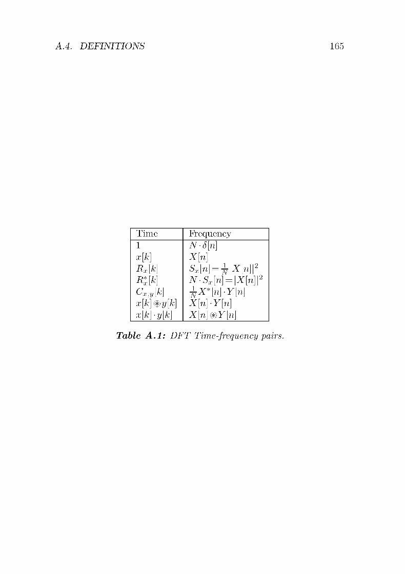
A.4. DEFINITIONS 165
Time Frequency1 N-Ô[n]x[k] X[n]Rx[k] Sx[n] = jj\X[n]\2R*x[k] N-Sx[n] = \X[n]\2Cx,y[k\ jjX*[n]-Y[n]x[k] ®y[k] X[n]-Y[n]x[k]-y[k] X[n]®Y[n]
Table A.l: DFT Time-frequency pairs.


Bibliography
[1] R. H. Waiden, "Performance Trends for Analog-to-Digital Con¬
verters," IEEE Communication Magazine, pp. 96-101, February1999.
[2] G. E. Moore, "No Exponential is Forever: But Forever Can Be
Delayed!" ISSCC, February 2003.
[3] B. Razavi, Principles of Data Conversion System Design, IEEE
Press, New York, 1995.
[4] A. V. Oppenhein, R. W. Schäfer, Discrete-Time Signal Process¬
ing, Prentice Hall, New Jersey, 1989.
[5] S. Rabii, B. A. Wooley, The Design of Low-Voltage, Low-Power
Sigma-Delta Modulators, Kluwer Academic Publisher, Boston,1999.
[6] W. Bennet, "Spectra of Quantized Signals," Bell System Tech.
Journal, Vol. 27, pp. 446-472, 1948.
[7] B. Widrow," A Study of Rough Amplitude Quantization by
Means of Nyquist Sampling Theory," IRE Trans. Circuit Theory,Vol. CT-3, pp. 266-276, December 1956.
[8] D. J. Goodman, "The Application of Delta Modulation to
Analog-to-Digital Encoding," Bell System Technical Journal,Vol. 48, pp. 321-343, February 1969.
167
168 BIBLIOGRAPHY
[9] J. C. Candy, "A Use of Limit Cycle Oscillations to Obtain
Robust Analog-to-Digital Converters," IEEE Trans. Commun.,Vol. COM-22, pp.298-305, March 1974.
[10] H. Inose, Y. Yasuda, and J. Murakami, "A Telemetering Sys¬tem by Code Modulation - AEModulation", IRE Transactions
on Space Electronics and Telemetry, Vol. SET-8, pp. 204-209,
September 1962.
[11] J. C. Candy, G. C. Temes, Oversampling Delta-Sigma Data Con¬
verters, IEEE Press, New York, 1992.
[12] J. C. Candy, O. J. Benjamin, "The Structure of QuantizationNoise from Sigma-Delta Modulation," IEEE Transactions on
Communications, Vol. COM-29, pp. 1316-1323, September 1981.
[13] R. M. Gray, "Oversampled Sigma-Delta Modulation," IEEE
Transactions on Communications, Vol. COM-35, pp. 481-489,
May 1987.
[14] W. Chou, P. W. Wong, R. M. Gray, "Multistage Sigma-Delta
Modulation," IEEE Transactions on Information Theory, Vol.
IT-35, pp. 784-796, July 1989.
[15] R. M. Gray, "Quantization Noise Spectra," IEEE Transactions
on Information Theory, Vol. IT-36, pp. 1220-1244, November
1990.
[16] S. R. Norsworthy, R. Schreier, G. C. Temes, Delta-Sigma Data
Converters, IEEE Press, New York, 1997.
[17] E. J. Van Der Zwan, E. C. Dijkmans, "A 0.2-mW CMOS EA
Modulator for Speech Coding with 80 dB Dynamic Range,"IEEE Journal of Solid-State Circuits, Vol. 31, No. 12, December
1996.
[18] J. A. Cherry, W. M. Snelgrove, Continuous-Time Delta-SigmaModulators for High-Speed A/D Conversion, Kluwer Academic
Publishers, 2000.
BIBLIOGRAPHY 169
[19] H. L. Fiedler and B. Höffhnger, "A CMOS Pulse Density Mod¬
ulator of High-Resolution A/D Converters," IEEE Journal of
Solid-State Circuits, Vol. SC-19, No. 6, December 1984.
[20] T. C. Leslie and B. Singh, "An Improved Sigma-Delta Modulator
Architecture," IEEE Proc. ISCAS'90, pp. 372-375, May 1990.
[21] T. Brooks, D. H. Robertson, D. F. Kelly, A. Del Muro, and S.
W. Hartson, "A Cascaded Sigma-Delta Pipeline A/D Converter
with 1.25 MHz Signal Bandwidth and 89 dB SNR," IEEE Jour¬
nal of Solid-State Circuits, Vol. 32, No. 12, December 1997.
[22] J. Das and P. K. Chatterjee, "Optimized AA Modulation Sys¬
tem," Electronic Letters, Vol. 3, pp. 286-287, June 1967.
[23] Y. Matsuya, K. Uchimura, A. Iwata, T. Kobayashi, M. Ishikawa,T. Yoshitome, "A 16-bit Oversampling A-to-D conversion Tech¬
nology Using Triple-Integration Noise Shaping," IEEE Journal
of Solid-State Circuits, Vol. SC-22, pp. 921-929, December 1987.
[24] A. Marques, V. Peluso, M. S. Steyaert, and W. Sansen, "OptimalParameters for AE Modulator Topologies," IEEE Transactions
on Circuit and Systems II: Analog and Digital Signal Processing,Vol. 45, No. 9, September 1998.
[25] I. Fujimori, L. Longo, A. Hairapetian, K. Seiyama, S. Kosic,J. Cao, and S.-L. Chan, "A 90-dB SNR 2.5-MHz Output-RateADC Using Cascaded Multibit Delta-Sigma Modulation at 8x
Oversampling Ratio," IEEE Journal of Solid-State Circuits, Vol.
35, No. 12, December 2000.
[26] F. Op't Eynde, G. M. Yin, W. Sansen, "A CMOS Fourth-Order
14b 500k-Sample/s Sigma-Delta ADC Converter," IEEE Inter¬
national Solid-State Circuit Conference Digest of Technical Pa¬
pers, pp. 62-63, February 1991.
[27] R. T. Baird, T. S. Fiez, "A Low Oversampling Ratio 14-b 500-
kHz EA ADC with a Self-Calibrated Multibit DAC," IEEE
Journal of Solid-State Circuits, Vol. 31, No. 3, pp. 312-320,
March 1996.

170 BIBLIOGRAPHY
[28] S. Au, and B. H. Leung, "A 1.95-V, o.34-mW, 12-b Sigma-DeltaModualtor Stabilized by Local Feedback Loops," IEEE Journal
of Solid-State Circuits, Vol. 32, No. 3, March 1997.
[29] A. Yasuda, H. Tanimoto, and T. Iida, "A Third-Order A-E
Modulator Using Second-Order Noise-Shaping Dynamic Ele¬
ment Matching," IEEE Journal of Solid-State Circuits, Vol. 33,No. 12, December 1998.
[30] Y. Geerts, M. S. J. Steyaert, and W. Sansen, "A High-Performance Multibit AE CMOS ADC," IEEE Journal of Solid-
State Circuits, Vol. 35, No. 12, December 2000.
[31] T. Cataltepe, A. R. Kramer, L. E. Larson, G. C. Temes, and R.
H. Waiden, "Digitally Corrected Multi-Bit EA Data Conveters,"IEEE Proc. ISCAS'89, pp. 647-650, May 1989.
[32] L. E. Larson, T. Cataltepe, G. C. Temes, "Multibit OversampledE-A A/D Convertor With Digital Error Correction," Electronics
Letters, Vol. 24, No. 16, pp. 1051-1052, August 1988.
[33] C. D. Thompson, S. R. Bernadas, "A Digitally-Corrected 20b
Delta-Sigma Modulator," IEEE International Solid-State Cir¬
cuit Conference Digest of Technical Papers, pp. 195-195, Febru¬
ary 1994.
[34] K. B. Klaassen, "Digitally Controlled Absolute Voltage Divi¬
sion," IEEE Transactions on Instrumentation and Measurement,Vol. 24, No.2, pp. 106-112, June 1975.
[35] R. J. Van De Plassche, "Dynamic Element Matching for High-
Accuracy Monolitic D/A Converters," IEEE Journal of Solid-
State Circuits, Vol. SC-11, No. 6, December 1976.
[36] F. J. Harris, "On the Use of Windows for Harmonic Analysiswith the Discrete Fourier Transform," Proceedings of the IEEE,Vol. 66, No. 11, January 1978.
[37] ETSI Documentation Service, "ETSI TS 101 388 VI.2.1", Oc¬
tober 2001.

BIBLIOGRAPHY 171
[38] D. Hester, "Analog Front End Design For ADSL," Proceedingsof VLSI Circuit Short Course, Honolulu, June 2000.
[39] R. W. Adams, P. F. Ferguson, A. Ganesan, S. Vincelette, A.
Volpe, R. Libert, "Theory and Practical Implementation of a
Fifth-Order Sigma-Delta A/D Converter," J. Audio Eng. Soc,
vol.39, No. 7 8, July August 1991.
[40] K. Y. Leung, E. J. Swanson, S. S. Zhu, "A 5V, 118dB Delta-
Sigma Analog-to-Digital Converter for Wideband Digital Au¬
dio," IEEE International Solid-State Circuits Conference, San
Francisco, 1997.
[41] J.H. Fischer, "Noise Sources and Calculation Techniques for
Switched Capacitor Filters," IEEE Journal of Solid State Cir¬
cuits, Vol.SC-17, August 1982.
[42] Y. Geerts, M. Steyaert, W. Sansen, Design of Multi-Bit Delta-
Sigma A/D Converters, Kluwer Academic, Boston, 2002.
[43] T. Burger, Optimal Design of Operational Transconductance
Amplifiers with Application for Low Power AE Modulators,
Hartung-Gorre Verlag, Konstanz, 2002.
[44] G. Nicollini, F. Moretti, M. Conti, "High-Frequency Fully Dif¬
ferential Filter Using Operational Amplifiers Without Common-
Mode Feedback," IEEE Journal of Solid-State Circuits, Vol. 24,No. 3, June 1989.
[45] E. Säckinger, W. Guggenbiihl, "A High-Swing, High ImpedanceMOS Cascode Circuit," IEEE Journal of Solid-State Circuit,
Vol.25, No.l, February 1990.
[46] K. Bult, G. J. G. M. Geelen, "A Fast-Settling CMOS Op Ampfor SC Circuits with 90-dB DC Gain," IEEE Journal of Solid
State Circuits, Vol.25, No.6, December 1990.
[47] J. Lloyd and H.-S. Lee, "A CMOS Op Amp with Fully-Differential Gain Enhancement," IEEE Transaction on Circuits
and Systems-II: Analog and Digital Signal Processing, Vol.41,
No.3, March 1994.
172 BIBLIOGRAPHY
[48] D. Senderowicz, S. F. Dreyer, J. H. Huggins, CF. Rahim, C.
A. Laber, "A Family of Differential NMOS Analog Circuits for a
PCM Codec Filter Chip," IEEE Journal of Solid-State Circuits,Vol. SC-17, No. 6, December 1982.
[49] S. M. Mallya, J. H. Nevin, "Design Procedures for a Fully Dif¬
ferential Folded-Cascode CMOS Operational Amplifier," IEEE
Journal of Solid-State Circuits, Vol. 24, No. 6, December 1989.
[50] T. C. Choi, R. T. Kaneshiro, R. W. Brodersen, P. R. Gray,W. B. Jett, M. Wilcox, "High-Frequency CMOS Switched-
Capacitor Filters for Communications Application," IEEE Jour¬
nal of Solid-State Circuits, Vol. 14, No. 6, December 1983.
[51] G. M. Yin, F. Op't Eynde, W. Sansen, "A High-Speed CMOS
Comparator with 8-b Resolution," IEEE Journal of Solid-State
Circuits, Vol. 27, No. 2, pp. 208-211, February 1992.
[52] B. P. Brandt, B. A. Wooley, "A 50-MHz Multibit Sigma-DeltaModulator for 12-b 2-MHz A/D Conversion," IEEE Journal of
Solid-State Circuits, Vol.26, No.12, pp. 1746-1756, December
1991.
[53] F. Medeiro, B. Perez-Verdu, A. Rodriguez-Vazquez, "A 13-bit,
2.2MS/s, 55-mW Multibit Cascade EA Modulator in CMOS
0.7um Single-Poly Technology," IEEE Journal of Solid-State
Circuits, Vol.34, No. 6, pp. 748-760, June 1999.
[54] A. Wiesbauer, H. Weinberger, M. Clara, J. Hauptmann,"A 13.5-Bit Cost Optimized Multi-Bit Delta-Sigma ADC for
ADSL," Proceedings of the ESSCIRC, pp. 86-88, Duisburg Ger¬
many, September 1999.
[55] Y. Geerts, A. M. Marques, M. S. J. Steyaert, W. Sansen, "A
3.3V, 15bit, Delta-Sigma ADC with a Signal Bandwidth of
1.1MHz for ADSL Applications," IEEE Journal of Solid-State
Circuits, Vol.34, No.7, pp. 927-936,July 1999.
[56] K. Vleugels, S. Rabii, B. A. Wooley, "A 2.5-V Sigma-Delta Mod¬
ulator for Broadband Communications Applications," IEEE

BIBLIOGRAPHY 173
Journal of Solid-State Circuits, Vol. 36, No. 12, pp. 1887-1999,December 2001.
[57] A. M. Marques, V. Peluso, M. S. J. Steyaert, W. Sansen, "A 15-
b Resolution 2-MHz Nyquist rate Delta-Sigma ADC in a 1-um
CMOS Technology," IEEE Journal of Solid-State Circuits, Vol.
33, No. 7, pp. 1065-1075, July 1998.
[58] ETSI Documentation Service, "ETSI TS 101 270-1 VI.2.1",1999-10.
[59] ETSI Documentation Service, "ETSI TS 101 270-2 VI.1.1",2001-02.
[60] J. G. Kenney, L. R. Carley, "Design of Multibit Noise-ShapingData Converters," Kluwer Academic Publisher: Analog Inte¬
grated Circuits and Signal Processing, Vol. 3, pp. 259-272, 1993.
[61] R. T. Baird, T. S. Fiez, "Linearity Enhancement of Multibit
AE A/D and D/A Converters Using Data Weighted Averaging,"IEEE Transactions on Circuits and Systems-II: Analog and Dig¬ital Signal Processing, Vol. 42, No. 12, pp. 753-762, December
1995.
[62] A. M. Abo, Design for Reliability of Low-Voltage, Switched-
Capacitor Circuits, Dissertation at California Institute of Tech¬
nology, Spring 1999.
[63] F. Piazza, Low Power RF-Receiver Front-End ICs for Mobile
Communications, Hartung-Gorre Verlag, Konstanz, 2000.
[64] I. E. Opris, L. D. Lewicki, "Bias Optimization for Switched
Capacitor Amplifiers," IEEE Transactions on Circuits and
Systems-II: Analog and Digital Signal Processing, Vol. 44, No.
12, pp. 985-989, December 1997.
[65] P. E. Allen and D. R. Holberg, CMOS Analog Circuit Design,Oxford University Press, New York, 1987.
[66] T. Burger, Q. Huang, "A 3V, 2.8mW CMOS Sigma-Delta-Modulator for GSM Applications", IEEE Symposium on VLSI
Circuits, Honolulu, 1998.

174 BIBLIOGRAPHY
[67] R. Reutemann, P. Balmelli, Q. Huang, "A 33mW 14b 2.5MSam-
ple/s EA A/D Converter in 0.25um Digital CMOS", ISSCC Di¬
gest of Technical Papers, pp. 316-317, Feb. 2002.
[68] A. R. Feldman, B. E. Boser, P. R. Gray, "A 13 bit, 1.4MS/s,3.3V Sigma-Delta Modulator for RF Baseband Channel Appli¬
cations," IEEE Journal of Solid-State Circuits, Vol. 33, No. 10,October 1998.
[69] L. Luh, J. Chôma Jr., J. Draper, "A 400MHz 5th-Order CMOS
Continuous-Time Switched-Current EA Modulator," Proceed¬
ings of the ESSCIRC, pp. 72-75, Stockholm, Sweden, September
2000.
[70] A. Di Giandomenico, S. Paton, A. Wiesbauer, L. Hernandez, T.
Pötscher, L. Dörrer, "A 15MHz Bandwidth Sigma-Delta ADC
with 11 Bits of Resolution in 0.13um CMOS," Proceedings of
the ESSCIRC, pp. 233-236, Estoril, Portugal, September 2003.

Curriculum Vitae
Pio Balmelli
Born July 12, 1973 in LuganoCitizen of Paradiso (TI), Switzerland
Sept. 1988 - June 1992 Secondary School (Liceo) of Canton Ti-
cino, Lugano
June 1992 Scientific Type Matura
Nov. 1992 - May 1998 Student at the Electrical Engineering
department of the Swiss Federal Insti¬
tute of Technology (ETH) Zurich
May 1998 Degree in Electrical Engineering from
ETH Zurich (dipl. El. Ing. ETH)
April 1998 - Dec. 2003 Ph.D. student and research assistant at
the Analog and Mixed Signal Design
group of the Integrated Systems Labo¬
ratory, headed by Prof. Dr. Q. Huang.
175


List of Publication
• [1] J. Meierhofer, U.P. Bernhard, P. Balmelli, D. Bernasconi,
"Priority Scheduling Algorithm for ATM Wireless Network Ac¬
cess," IEEE 1997 International Conference on Universal Per¬
sonal Communications, San Diego (CA), October 1997.
• [2] P. Balmelli, Q. Huang and F. Piazza, "A 50-mW 14-bit 2.5-
MS/s E-A Modulator in a 0.25um Digital CMOS Technology,"IEEE 2000 Symposium on VLSI Circuits Digest of Technical
Papers, pp. 142-143, Honolulu (HI), June 2000.
• [3] R. Reutemann, P. Balmelli, Q. Huang, "A 33mW 14b 2.5MSam-
ple/s EA A/D Converter in 0.25um Digital CMOS," ISSCC
Digest of Technical Papers, pp. 316-317, San Francisco (CA),February 2002.
• [4] P. Balmelli, Q. Huang, "A 25MS/s 14b 200mW EA Modu¬
lator in 0.18um CMOS," ISSCC Digest of Technical Papers, pp.
74-75, San Francisco (CA), February 2004.
177