implementation & eco design experience sharing...
TRANSCRIPT

1
RoHSRoHSImplementation & Eco DesignImplementation & Eco Design
Experience SharingExperience SharingCDILCDIL
What is RoHS ?What is RoHS ?Directive 2002/95/EC of the European parliament and of theDirective 2002/95/EC of the European parliament and of thecouncil (27 January 2003)council (27 January 2003)
Member States shall ensure that, from Member States shall ensure that, from 11stst JulyJuly20062006,, new electrical and electronic equipment put on new electrical and electronic equipment put on
the market does not contain the market does not contain 1.1. Lead, Lead, 2.2. Mercury, Mercury, 3.3. Cadmium, Cadmium, 4.4. Hexavalent ChromiumHexavalent Chromium5. 5. Polybrominated biphenyls (PBB) Polybrominated biphenyls (PBB) 6.6. Polybrominated diphenyl ethers (PBDEPolybrominated diphenyl ethers (PBDE).).

2
Supply Chain Environment ManagementSupply Chain Environment Management[ Implications of EU[ Implications of EU’’s RoHS & WEEE s RoHS & WEEE
Directives]Directives]## In 2001 CDIL carried out a joint study with ELCINA (Electronic CIn 2001 CDIL carried out a joint study with ELCINA (Electronic Component omponent
Industries Association, India); NetPEM (Network for Preventive Industries Association, India); NetPEM (Network for Preventive Environment Management) a Nagpur based NGO and IIIEE (InternatioEnvironment Management) a Nagpur based NGO and IIIEE (International nal Institute for Industrial Environmental Economics) Lund UniversitInstitute for Industrial Environmental Economics) Lund University, Lund, y, Lund, Sweden to understand the implications of European Union RoHS & WSweden to understand the implications of European Union RoHS & WEEE EEE Directives on Indian Electronic Components Manufacturers ( with Directives on Indian Electronic Components Manufacturers ( with special special reference to CDIL)reference to CDIL)
## Prof. Lars Prof. Lars HanssonHansson & Prof. Thomas Lindhqvist of Lund University Sweden & Prof. Thomas Lindhqvist of Lund University Sweden visited CDIL to facilitate the understanding of the product orievisited CDIL to facilitate the understanding of the product oriented environment nted environment legislations in specific and the study as a wholelegislations in specific and the study as a whole
## Prof. Hansjorg Griese of Fraunhofer Institute Berlin also visiteProf. Hansjorg Griese of Fraunhofer Institute Berlin also visited CDIL and have d CDIL and have facilitated in building understanding of GREEN ELECTRONICS facilitated in building understanding of GREEN ELECTRONICS
## The outcome of this study and the understanding build up was dThe outcome of this study and the understanding build up was disseminated in isseminated in a seminar organized by ELCINA in 2002 among the member industriea seminar organized by ELCINA in 2002 among the member industries.s.
CDILCDIL’’s RoHS Issuess RoHS Issues
Five Key Challenges of CDIL semiconductor Five Key Challenges of CDIL semiconductor devices with respect to RoHS compliancedevices with respect to RoHS complianceElimination of RoHS material from processElimination of RoHS material from processDevelopment of alternative Material & Process Development of alternative Material & Process particularly lead free processparticularly lead free processForward & Backward Compatibility, Forward & Backward Compatibility, Supply Chain Management, Supply Chain Management, Cost of compliance, Cost of compliance,

3
Elimination of ChromiumElimination of Chromium-- The first The first stepstep
Historically CDIL used Potassium Dichromate Historically CDIL used Potassium Dichromate solution in solution in HClHCl as pre cleaners in axial diodes as pre cleaners in axial diodes
prior to lead prior to lead finish. finish.
Action Taken : In Oct 2002 ,a non hazardous chemical MICROPREP 18 was tried and found as a substitute .
Result : • Chrome eliminated from process.• Customer demand was fulfilled.• The Cost is reduced both Mfg. and Effluent Treatment Aprox. 1 lakh per year•All the quality parameters are comparable.• The solderability after dry aging and steam aging,•Finish, Coverage , Solder thickness and Reliability results were found OK.
Cadmium in InkCadmium in Ink-- The Sony episodeThe Sony episodeIn Jan 2003 Sony (India) awarded Green Partner status toIn Jan 2003 Sony (India) awarded Green Partner status toCDIL. CDIL.
In Oct 2002 CDIL found that the printing ink in the packaging of a consignment meant for Sony contained more than 9 ppm of Cadmium as per a test report from a Lab.
On probing it was found that the Lab was using BS EN 1122 : 2001 ["Plastics-Determination of cadmium - Wet decomposition method" ] . This is done by Atomic Absorption Spectrometer (AAS)
On further investigation we found Inductively Coupled Plasma Atomic EmissionSpectrometer [ ICP-AES ] is the more reliable instrument for such test.But this was available with Sony only. On contacting, Sony agreed to help us and It was found that there was error in the earlier report. Also the cadmium was found only in the refilled cartridge and not in the original cartridge.
4
Material & Process DevelopmentMaterial & Process Development
CDIL hasCDIL has ADOPTED Lead free manufacturingADOPTED Lead free manufacturingand all its devices have become lead free and all its devices have become lead free wefwef 11stst July 2005. July 2005. Earlier Terminal Finish : Sn/PbEarlier Terminal Finish : Sn/Pb----90/10 90/10 RoHS Compliant Lead free Terminal Finish : Matte RoHS Compliant Lead free Terminal Finish : Matte SnSnManufacturing issues to be addressed on an ongoing basisManufacturing issues to be addressed on an ongoing basis
---- Growth of Tin whiskersGrowth of Tin whiskers---- PbPb free solders typically have a higher melting point. The free solders typically have a higher melting point. The
consequentconsequent higher temperature processinghigher temperature processing requires requires enhanced heat resistance in components and enhanced heat resistance in components and improvement/modification to PCB assembly equipmentimprovement/modification to PCB assembly equipment and and materials.materials.
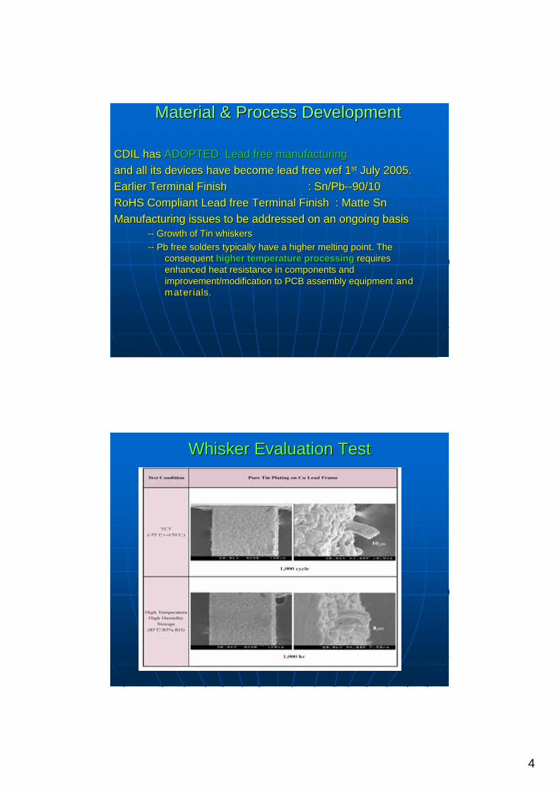
Whisker Evaluation TestWhisker Evaluation Test
5
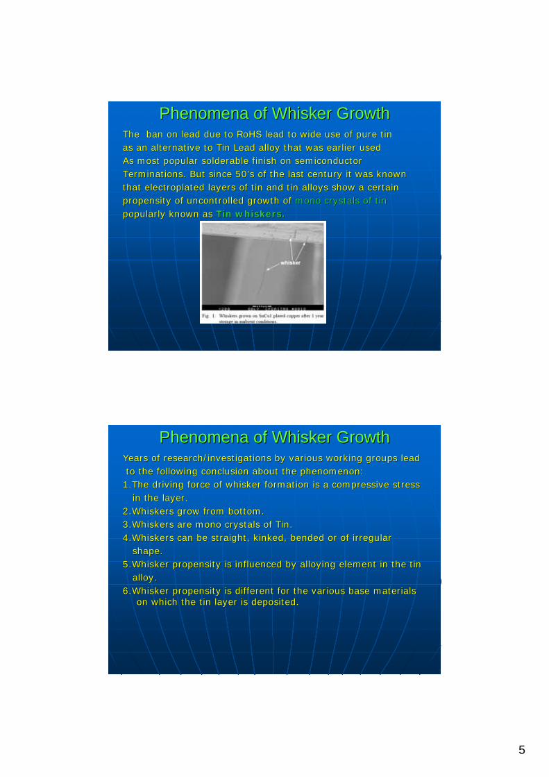
Phenomena of Whisker GrowthPhenomena of Whisker GrowthThe ban on lead due to RoHS lead to wide use of pure tinThe ban on lead due to RoHS lead to wide use of pure tinas an alternative to Tin Lead alloy that was earlier used as an alternative to Tin Lead alloy that was earlier used As most popular solderable finish on semiconductorAs most popular solderable finish on semiconductorTerminations. But since 50Terminations. But since 50’’s of the last century it was known s of the last century it was known that electroplated layers of tin and tin alloys show a certainthat electroplated layers of tin and tin alloys show a certainpropensity of uncontrolled growth ofpropensity of uncontrolled growth of mono crystals of tinmono crystals of tinpopularly known aspopularly known as Tin whiskers.Tin whiskers.
Phenomena of Whisker GrowthPhenomena of Whisker GrowthYears of research/investigations by various working groups leadYears of research/investigations by various working groups leadto the following conclusion about the phenomenon:to the following conclusion about the phenomenon:
1.The driving force of whisker formation is a compressive stress1.The driving force of whisker formation is a compressive stressin the layer.in the layer.
2.Whiskers grow from bottom.2.Whiskers grow from bottom.3.Whiskers are mono crystals of Tin.3.Whiskers are mono crystals of Tin.4.Whiskers can be straight, kinked, bended or of irregular 4.Whiskers can be straight, kinked, bended or of irregular
shape.shape.5.Whisker propensity is influenced by alloying element in the ti5.Whisker propensity is influenced by alloying element in the tin n
alloy.alloy.6.Whisker propensity is different for the various base materials6.Whisker propensity is different for the various base materials
on which the tin layer is deposited.on which the tin layer is deposited.

6
Phenomena of Whisker GrowthPhenomena of Whisker Growth
Whisker MitigationWhisker Mitigation
Post plate (Matte Post plate (Matte SnSn) bake ) bake –– 15015000C / 60 minutes C / 60 minutes Developed and promoted by E4 Developed and promoted by E4 –– ST ST
Microelectronics, Philips Semiconductors, Infineon Microelectronics, Philips Semiconductors, Infineon Technologies, Freescale Semiconductors.Technologies, Freescale Semiconductors.
Applicable to Lead frames based on Cu and Applicable to Lead frames based on Cu and Alloy 42 (FeNi42)Alloy 42 (FeNi42)
Matte Sn most preferredWhisker mitigation -
7
Mitigation of Whisker GrowthMitigation of Whisker GrowthDuring the bake, the major effect is the artificial growth of thDuring the bake, the major effect is the artificial growth of the intermetallic double e intermetallic double layer Cu3Sn / Cu6Sn5 at the Cu layer Cu3Sn / Cu6Sn5 at the Cu –– SnSn interface. interface. This intermetallic grows uniformly at 150 deg C and forms a contThis intermetallic grows uniformly at 150 deg C and forms a continuous layer, which inuous layer, which acts as a diffusion barrier for further Cu acts as a diffusion barrier for further Cu –– diffusion into Tin . This copper diffusion is diffusion into Tin . This copper diffusion is associated with the intermetallic formation and happens only in associated with the intermetallic formation and happens only in the Tin grain the Tin grain boundaries at Room Temperature i.e. irregular growth of intermetboundaries at Room Temperature i.e. irregular growth of intermetallics. allics. At higher temperatures (150 C) there is a shift from grain boundAt higher temperatures (150 C) there is a shift from grain boundary diffusion in ary diffusion in favour of bulk diffusion resulting in a uniform layer. Since thfavour of bulk diffusion resulting in a uniform layer. Since the intermetallic formation e intermetallic formation is associated with a volume increase, The irregularities induce is associated with a volume increase, The irregularities induce stress and have to be stress and have to be avoided. avoided. This can be achieved by introduction of barrier metals (Ni, Ag This can be achieved by introduction of barrier metals (Ni, Ag ……) or by the artificial ) or by the artificial growth of the inter metallic itself.growth of the inter metallic itself.
In addition, the phenomenon of recrystallization, dislocation slIn addition, the phenomenon of recrystallization, dislocation slide and climb and ide and climb and recombination occur at 150 C resulting in a stress relieve. recombination occur at 150 C resulting in a stress relieve.
Matte Tin has larger grains (> 1 micron) compared to Bright Tin Matte Tin has larger grains (> 1 micron) compared to Bright Tin (<0.5 micron). (<0.5 micron). Smaller grains provide more grain boundaries leading to whiskeriSmaller grains provide more grain boundaries leading to whiskering. Optimum grainng. Optimum grainsize 2 size 2 –– 5 micron. Also, carbon content should be <300 ppm.5 micron. Also, carbon content should be <300 ppm.
In the FeNi42 Lead frame the whisker formation occurs during TMCIn the FeNi42 Lead frame the whisker formation occurs during TMCL due to L due to large large
CTE mismatch of FeNi42 and CTE mismatch of FeNi42 and SnSn..
SOLDER COMPATIBILITYSOLDER COMPATIBILITY
FORWARD COMPATIBILITY:FORWARD COMPATIBILITY: COMPATIBILITY COMPATIBILITY JUDGED WHEN COMPONENT FINISH IS JUDGED WHEN COMPONENT FINISH IS NOTNOTLEADLEAD--FREE AND SOLDER USED IS LEADFREE AND SOLDER USED IS LEAD--FREEFREE
B A C K W A R D C O M P A T I B I L I T Y :B A C K W A R D C O M P A T I B I L I T Y :C O M P A T I B I L I T Y J U D G E D W H E N C O M P A T I B I L I T Y J U D G E D W H E N COMPONENT FINISH IS LEAD FREE AND COMPONENT FINISH IS LEAD FREE AND S O L D E R U S E D I S N O N L E A D F R E ES O L D E R U S E D I S N O N L E A D F R E E
All CDIL products, All CDIL products, PbPb--free & non free & non PbPb--free are free are Forward compatible and Backward compatible.Forward compatible and Backward compatible.
8
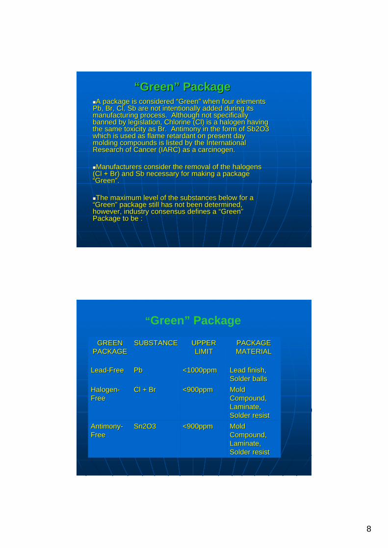
““GreenGreen”” PackagePackageA package is considered A package is considered ““GreenGreen”” when four elements when four elements
Pb, Br, Cl, Sb are not intentionally added during its Pb, Br, Cl, Sb are not intentionally added during its manufacturing process. Although not specifically manufacturing process. Although not specifically banned by legislation, Chlorine (Cl) is a halogen having banned by legislation, Chlorine (Cl) is a halogen having the same toxicity as Br. Antimony in the form of Sb2O3 the same toxicity as Br. Antimony in the form of Sb2O3 which is used as flame retardant on present day which is used as flame retardant on present day molding compounds is listed by the International molding compounds is listed by the International Research of Cancer (IARC) as a carcinogen. Research of Cancer (IARC) as a carcinogen.
Manufacturers consider the removal of the halogens Manufacturers consider the removal of the halogens ((ClCl + Br) and Sb necessary for making a package + Br) and Sb necessary for making a package ““GreenGreen””..
The maximum level of the substances below for a The maximum level of the substances below for a ““GreenGreen”” package still has not been determined, package still has not been determined, however, industry consensus defines a however, industry consensus defines a ““GreenGreen””Package to be : Package to be :
Mold Mold Compound, Compound, Laminate, Laminate, Solder resistSolder resist
<900ppm<900ppmSn2O3Sn2O3AntimonyAntimony--FreeFree
Mold Mold Compound, Compound, Laminate, Laminate, Solder resistSolder resist
<900ppm<900ppmCl + BrCl + BrHalogenHalogen--FreeFree
Lead finish, Lead finish, Solder ballsSolder balls
<1000ppm<1000ppmPbPbLeadLead--FreeFree
PACKAGE PACKAGE MATERIALMATERIAL
UPPER UPPER LIMITLIMIT
SUBSTANCESUBSTANCEGREEN GREEN PACKAGEPACKAGE
“Green” Package
9
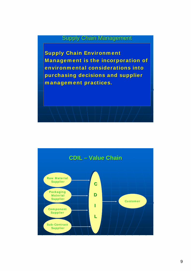
Supply Chain ManagementSupply Chain Management
Supply Chain Environment Supply Chain Environment Management is the incorporation of Management is the incorporation of environmental considerations into environmental considerations into purchasing decisions and supplier purchasing decisions and supplier management practices.management practices.
CDIL CDIL –– Value ChainValue Chain
C
D
I
L
CC
DD
II
LL
Raw MaterialSupplier
PackagingMaterialSupplier
Customer
ComponentSupplier
Sub-ContractSupplier

10
System for Tracking & Reporting System for Tracking & Reporting ComplianceCompliance
ProcurementProcedure for Raw Material
ProcurementProcedure for
Packaging Material
ProcurementProcedure for
Semiconductors
Procedure for Subcontracting
Procedure for Reporting Compliance to
Customer
System for Tracking & Reporting System for Tracking & Reporting ComplianceCompliance
Raw Material Supplier
Packaging MaterialSupplier
SemiconductorsSupplier
Sub-Contractors
Material Content Declaration
Certificate of Compliance
Material Content Declaration
Certificate of Compliance
Qualification Documents
11
Technical FileTechnical File
Material Content Declaration of Each Homogenous MaterialMaterial Content Declaration of Each Homogenous Material
Certificate of ComplianceCertificate of Compliance
Qualification Document [Lead Free Component]Qualification Document [Lead Free Component]
Format for Reporting Compliance to Format for Reporting Compliance to CustomerCustomer
Material Content Declaration RoHS / ELV Banned Substance Declaration (in mg/kg)
Remarks
Parts Name(Homogenous Material) & Weight (in mg)
Chemical Substance Occurr
ence in %
Pb Cd Hg Cr+6 PBB PBDE
Package Name: Package Weight:

12
Initiative for ResourceInitiative for ResourceConservationConservation
Total Raw water usage in Total Raw water usage in KL / Million Chips ProductionKL / Million Chips Production
13
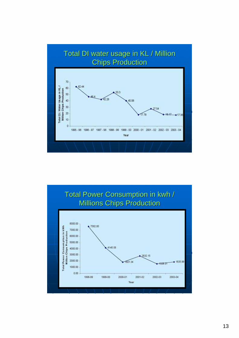
Total DI water usage in KL / Million Total DI water usage in KL / Million Chips ProductionChips Production
Total Power Consumption in kwh / Total Power Consumption in kwh / Millions Chips ProductionMillions Chips Production
14
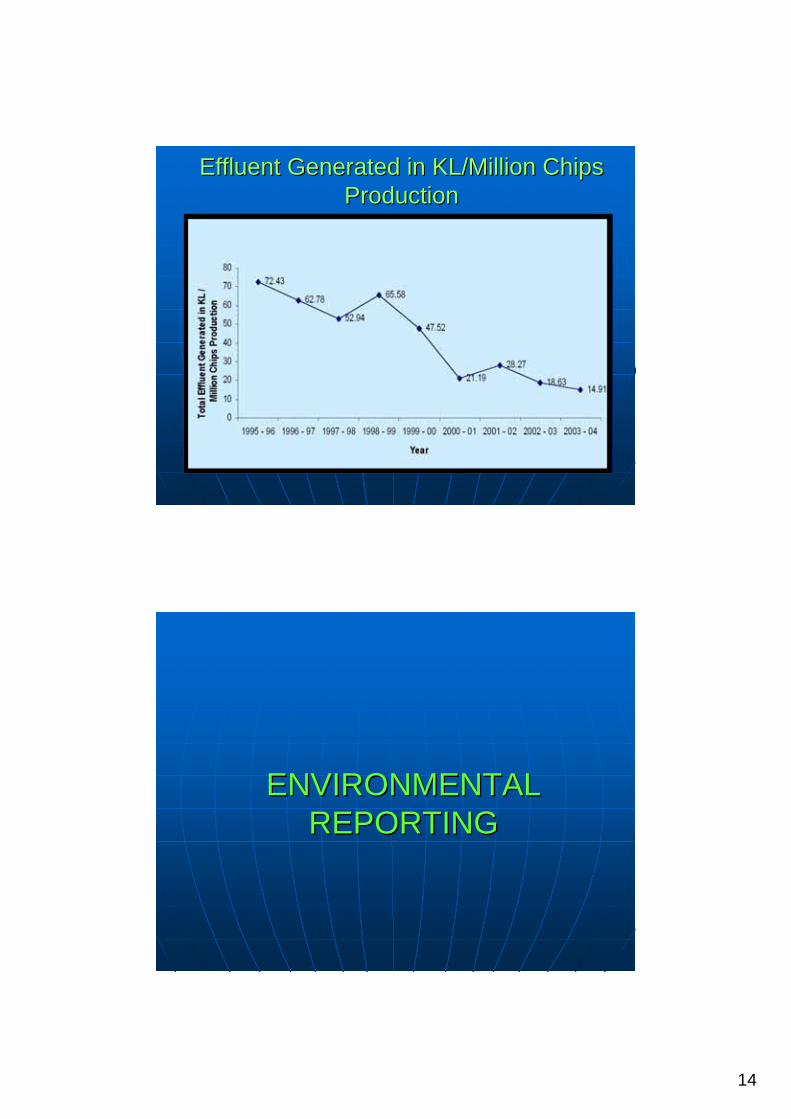
Effluent Generated in KL/Million Chips Effluent Generated in KL/Million Chips ProductionProduction
ENVIRONMENTAL ENVIRONMENTAL REPORTINGREPORTING

15
BACKGROUNDBACKGROUNDIn view of heightened public and societal In view of heightened public and societal concern for environmental issues, the World concern for environmental issues, the World Business Council for Sustainable Development Business Council for Sustainable Development (WBSCD) along with the Coalition for (WBSCD) along with the Coalition for Environmentally Responsible Economics Environmentally Responsible Economics (CERES) has proposed the Global Reporting (CERES) has proposed the Global Reporting Initiative (GRI). The GRI was established in Initiative (GRI). The GRI was established in 1997 with a mission to elevate sustainability 1997 with a mission to elevate sustainability reporting to equivalency with financial reporting. reporting to equivalency with financial reporting. In 2001, the Harvard Business School espoused In 2001, the Harvard Business School espoused the concept of the Triple Bottom Line (TBL) the concept of the Triple Bottom Line (TBL) which comprises the three axes of People, which comprises the three axes of People, Planet and Profits. Planet and Profits.
Several Indian companies have adopted TBL concepts in Several Indian companies have adopted TBL concepts in their Annual reports. The TBL is an adjunct to the earlier their Annual reports. The TBL is an adjunct to the earlier Balanced Score Card (BSC).Balanced Score Card (BSC).
There are four constituents of Reporting :There are four constituents of Reporting :a)a) Quantitative burden Quantitative burden b)b) Environmental accounting, including cost Environmental accounting, including cost –– benefit benefit
analysis (benefit includes Economic benefit and analysis (benefit includes Economic benefit and Environmental Impact Reduction).Environmental Impact Reduction).
c)c) Qualitative listing of all initiatives in the area of Qualitative listing of all initiatives in the area of Environment, Safety, Health and Social Environment, Safety, Health and Social Contributions.Contributions.
d)d) Environment Cost analysis similar to Quality CostEnvironment Cost analysis similar to Quality Cost
In due course the reporting of In due course the reporting of Quantitative Quantitative Burden will become mandatoryBurden will become mandatory. The others . The others are guidance for internal controls.are guidance for internal controls.
16
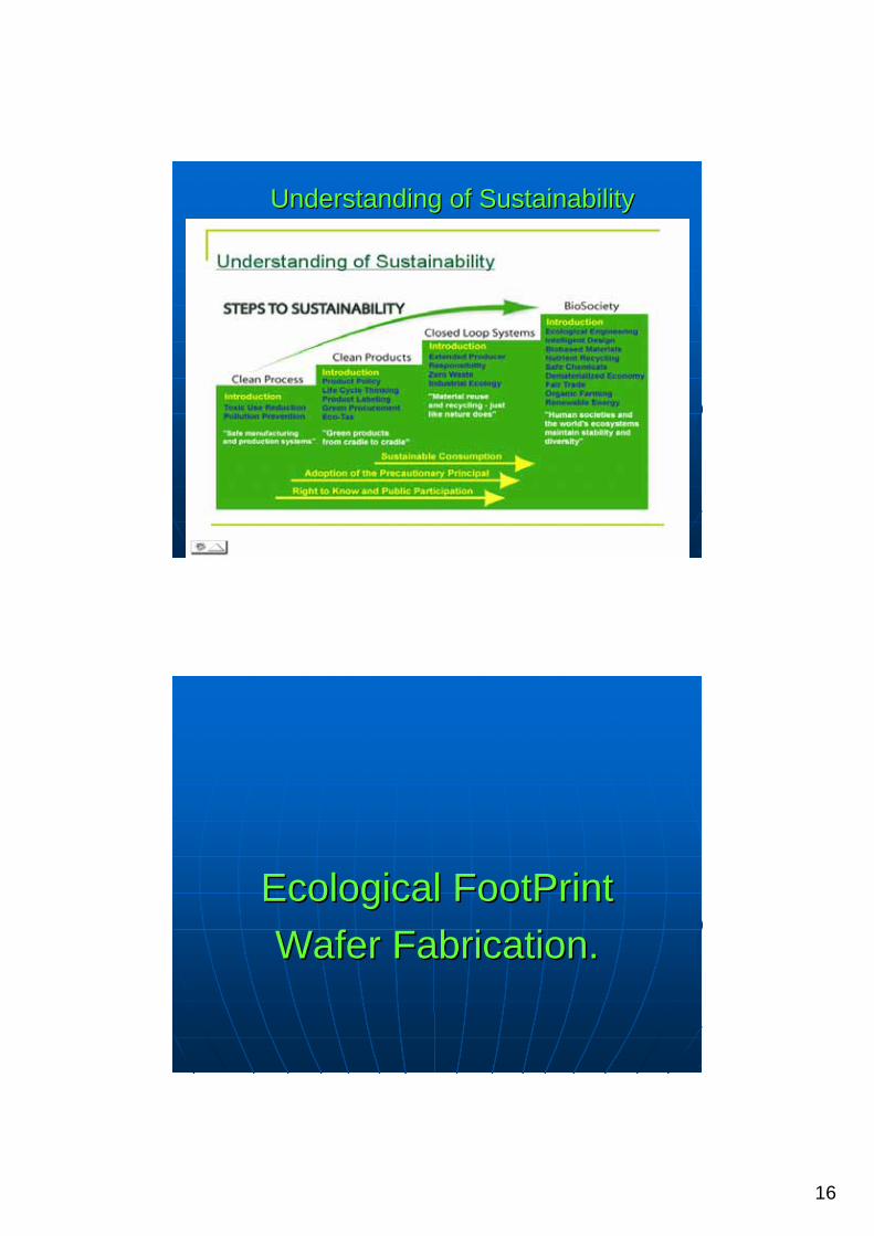
Understanding of SustainabilityUnderstanding of Sustainability
Ecological FootPrint Ecological FootPrint Wafer Fabrication.Wafer Fabrication.

17
Environmental burdenEnvironmental burdenThe The environmental burden methodenvironmental burden method is used to is used to estimate the potential environmental impactestimate the potential environmental impact of of emissions and wastes, rather than just stating emissions and wastes, rather than just stating quantities against local legislation limits. quantities against local legislation limits.
This is an informative and scientifically sound This is an informative and scientifically sound way of quantifying the environmental way of quantifying the environmental performance of a company and can be used performance of a company and can be used to set and monitor targets for improvementto set and monitor targets for improvement..
A total of A total of 7 impact categories7 impact categories are used are used ––Five Five dealing with emissions to air and two to waterdealing with emissions to air and two to water..
1452.201452.20
2.602.60
94.394.3
0.100.10
32972.032972.0
20042004--0505
Kg Ethylene Kg Ethylene EqEq
Kg SO2 EqKg SO2 Eq
Kg VOCKg VOC
Kg RKg R--11 Eq11 Eq
Kg CO2 EqKg CO2 Eq
UNITS*UNITS*(Per 1000 Wafer)(Per 1000 Wafer)
2086.302086.30
2.302.30
92.292.2
0.100.10
27787.627787.6
20052005--0606
Urban smog; Urban smog; healthhealth
Photochemical Photochemical Ozone CreationOzone Creation
Acid rain; Acid rain; healthhealth
Atmospheric Atmospheric acidificationacidification
Urban smog; Urban smog; health & safetyhealth & safety
Total VOC Total VOC emissionsemissions
Climate & Climate & healthhealth
Ozone DepletionOzone Depletion
Climate Climate changechange
Global WarmingGlobal Warming
POTENTIAL POTENTIAL EFFECTSEFFECTS
BURDENBURDEN
Environmental Burdens Wafer Fab
(Comparison FY 04-05 and 05-06)

18
7.407.40
15.7015.70
20042004--0505
Kg Kg PhosphaPhospha
te Eqte Eq
Kg BODKg BOD
UNITS*UNITS*(Per (Per 1000 1000
Wafer)Wafer)
7.107.10
15.1015.10
20052005--0606
Removes Removes oxygen from oxygen from waterwater
Aquatic EutrophicationAquatic Eutrophication
Threat to fish Threat to fish and aquatic and aquatic lifelife
Aquatic Oxygen DemandAquatic Oxygen Demand
POTENTIAL POTENTIAL EFFECTSEFFECTS
BURDENBURDEN
* For meaningful control we need to monitor prorata e.g. MTCE/1000 wafers or MTCE / MReAV
Environmental Burdens Wafer Fab (Comparison 04-05 & 05-06)
Wafer Fab. Environmental Impacts (Comparison FY 04-05 & FY 05-06)
0.01570.0157
0.00740.0074
1.4521.452
0.00260.0026
0.00010.0001
0.09430.0943
32.97232.972
Per wafer 2004Per wafer 2004--0505
0.01520.0152Kg BODKg BODAquatic Oxygen DepletionAquatic Oxygen Depletion
0.00710.0071Kg Phosphate Kg Phosphate EqEq
Aquatic EutrophicationAquatic Eutrophication
2.08632.0863Kg Ethylene EqKg Ethylene EqPhotochemical Ozone Photochemical Ozone CreationCreation
0.00230.0023Kg SOKg SO22 EqEqAtmospheric Acidification Atmospheric Acidification
0.00010.0001Kg CFCKg CFC--11 Eq11 EqOzone DepletionOzone Depletion
0.09220.0922Kg VOCKg VOCTotal VOC EmissionsTotal VOC Emissions
27.78827.788Kg CO2 EqKg CO2 EqGlobal Warming Global Warming
Per Wafer 2005Per Wafer 2005--0606UNITSUNITSEnvironmental Burden / Environmental Burden / ImpactsImpacts
19
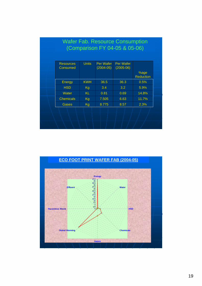
Wafer Fab. Resource Consumption (Comparison FY 04-05 & 05-06)
2.3%2.3%8.578.578.7758.775KgKgGasesGases11.7%11.7%6.636.637.5057.505KgKgChemicalsChemicals14.8%14.8%0.690.690.810.81KLKLWaterWater5.9%5.9%3.23.23.43.4KgKgHSDHSD0.5%0.5%36.336.336.536.5KWHKWHEnergyEnergy
%age %age ReductionReduction
Per Wafer Per Wafer (2005(2005--06)06)
Per Wafer Per Wafer (2004(2004--05)05)
UnitsUnitsResources Resources ConsumedConsumed
02.5
57.510
12.515
17.520
22.525
27.530
32.535
37.5Energy
Water
HSD
Chemicals
Gases
Global Warming
Hazardous Waste
Effluent
ECO FOOT PRINT WAFER FAB (2004-05)
20
0.02.55.07.5
10.012.515.017.520.022.525.027.530.032.535.037.5Energy
Water
HSD
Chemicals
Gases
Global Warming
Hazardous Waste
Effluent
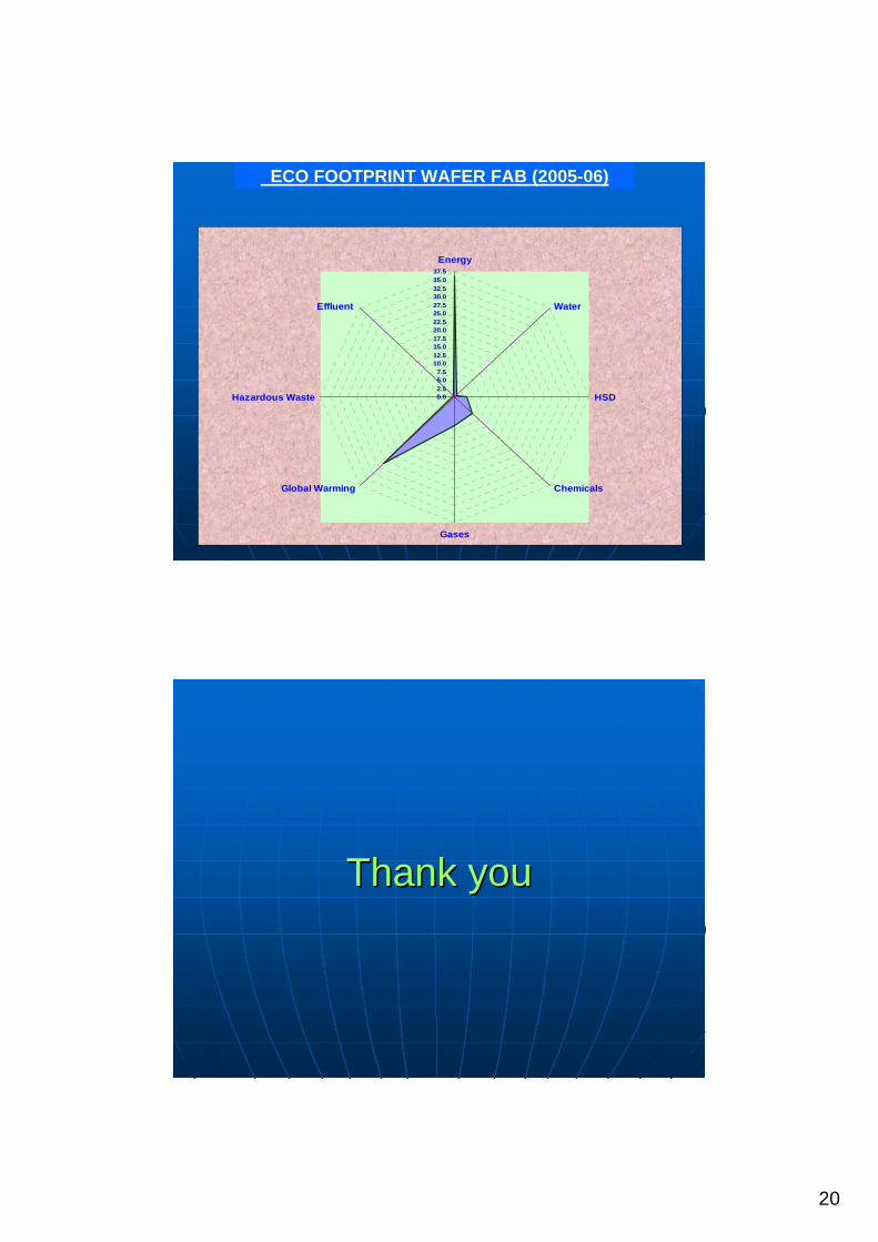
ECO FOOTPRINT WAFER FAB (2005-06)
Thank youThank you