imaging the interfaces of conjugated polymer optoelectronic devices
TRANSCRIPT
DOI: 10.1002/adma.200700887
Imaging the Interfaces of Conjugated Polymer OptoelectronicDevices**
By David W. Steuerman, Andres Garcia, Mark Dante, Renqiang Yang, Jan P. Löfvander,and Thuc-Quyen Nguyen*
As the science of polymeric optoelectronic devices continu-ously matures, performance often improves at the expense ofincreasingly more complex device architectures. One wide-spread approach toward optimization is the use of severalpolymers, either in the form of blends or multiple layers.[1,2] Inthe multilayer approach, each polymer is individually tailoredto address specific functions such as charge carrier injection/transport, carrier separation, light absorption, or emission.A central assumption behind this approach is an understand-ing of the resulting complex interfaces. Historically, to achieveimproved device efficiency in polymer light emitting diodes(PLEDs), a variety of surface treatments of electrodes andchemical modifications of polymers to tailor their ionizationpotential and/or electron affinity have been pursued.[3] Ex-periments designed to extract the mechanistic rationale be-hind the observed improvements can lead to differing conclu-sions.[4–16] The inherent difficulty of performing analyticalmeasurements on materials embedded between electrodescontributes in part to these controversies. Recent advances insubsurface imaging by scanning near-field ultrasound hologra-phy[17] may shed some light on the interfacial structure ofthese systems. There has also been related progress by usingneutron reflectivity. [18] Other techniques used to characterizepolymer-polymer interfaces are soft X-Ray reflectivity,[19–21]
secondary ion mass spectroscopy (SIMS),[22–26] and ellipsome-try.[27,28] However, these techniques have been used mainly tocharacterize traditional non-conducting polymers. At present
there have been few attempts to directly image polymer-poly-mer interfaces inside device structures,[29–33] and currentlythere are no high resolution images of operational multilayerpolymer light-emitting diodes (PLEDs). Typically, a PLED isbuilt upon a transparent ITO electrode modified by a bufferlayer, such as poly(3,4-ethylenedioxythiophene)-poly(styrene-sulfonate) (PEDOT:PSS); these two components comprisethe anode. Subsequently, hole transport, emissive layer andelectron transport/injection layers (ETL/EIL) are depositedby spin casting, followed by the deposition of the cathode, al-though many variations exist. The efficiencies of multilayerPLEDs have been substantially higher than those of singlelayer counterparts.[1,2,34] Often, small molecules deposited bythermal evaporation[35] or surfactants[36] or ionomers[37,38] areused as the ETL. The use of conjugated polymers as the ETLis less common, primarily because when multilayers are spuncast from organic solvents, some mixing of the components isunavoidable as well as removal of the underlying layer.Recently, conjugated polyelectrolytes (CPs) or charged conju-gated polymers, i.e., conjugated polymers with charged func-tional groups, have been used to improve electron injectionand transport in PLEDs.[1,2] Due to the presence of thecharged functional groups, which can be ionized in high di-electric media, CPs are soluble in water and polar organic sol-vents. Advantages of using CPs as the ETL in PLEDs includethe ability to form multilayer devices by solution methods thatalternate solvent polarity, the presence of the charge func-tional groups which incorporate dipoles at adjacent to theelectrode surface and the presence of mobile counterions forcompensating injected charge carriers. Throughout much ofthe reported work, it is the working assumption that the cast-ing of the CP layer does not disrupt the underlying neutralconjugated polymer layer. In this communication we report ageneral technique to image and thus examine the different in-terfaces of these devices. We employ a dual beam scanningelectron microscope/focused-ion beam (SEM/FIB) to create150 nm thick cross-sections that can be investigated by trans-mission electron microscopy (TEM). This proven method ofmanufacturing TEM samples is widely accepted[39] and amainstay of defect analysis in the semiconductor industry. Theresults obtained by cross-sectional TEM imaging are com-pared to atomic force microscopy (AFM) thickness profilesand dynamic secondary ion mass spectrometry (SIMS) analy-sis. We apply this cross-sectional analysis to a series of conju-gated polymer device structures and processing options todemonstrate the versatility of the technique in probing the in-
CO
MM
UN
ICATI
ON
528 © 2008 WILEY-VCH Verlag GmbH & Co. KGaA, Weinheim Adv. Mater. 2008, 20, 528–534
–[*] Prof. T.-Q. Nguyen, A. Garcia, M. Dante, Dr. R. Yang
Center for Polymers and Organic Solids andMitsubishi Chemical Center for Advanced MaterialsDepartment of Chemistry & Biochemistry, University of California,Santa BarbaraSanta Barbara, CA 93106-9510 (USA)E-mail: [email protected]. D. W. SteuermanDepartment of Physics, University of California, Santa BarbaraSanta Barbara, CA 93106-9530 (USA)Dr. Jan P. LöfvanderMaterials Research Laboratory, University of California, SantaBarbaraSanta Barbara, CA 93106-5121 (USA)
[**] The authors thank Dr. Tom Mates for his guidance with SIMS mea-surements and the Mitsubishi Chemical Center for AdvancedMaterials, the Office of Naval Research Young InvestigatorAward, and the National Science Foundation CAREER Award(DMR# 0547639) for financial support.
ternal structures including polymer-polymer and polymer-metal interfaces as a function of processing conditions andchoice of materials. We found that a principle rule for fabri-cating multilayer PLEDs with well defined device interfacesis to match the solvent polarity so that it does not interactwith the underlying polymer layer. This rule applies for a sin-gle polymer component as well as for a polymer blend. Ther-mal annealing reduces intermixing of two polymer layerswhen both layers are spun cast from the same solvent or sol-vents with similar polarity.
To examine the type of polymer-polymer interfaces thatarise when both polymers are spun cast from similar solventswith similar polarity, poly[2-methoxy-5-(2′-ethyl-hexyloxy)-1,4-phenylene vinylene] (MEH-PPV) was spun cast from tolu-ene onto an ITO-coated glass substrate followed by a layer ofpoly(3-hexylthiophene) (P3HT) spun cast from toluene orpoly[9,9-bis(6′-hexyl)fluorene-co-alt-phenylene] (PFP) spuncast from tetrahydrofuran (THF). For the polymer-polymerinterface formed from different solvent polarity, the first layeris MEH-PPV and the second layer is poly[9,9-bis(6′-(N,N,N-trimethylammonium)-hexyl)fluorene-co-alt-phenylene] dibro-mide (PFN+Br–) spun cast from methanol. The interfacebetween PEDOT:PSS and a layer previously used to incorpo-rating phosphorescent dopants was examined by lookingat a blend comprising poly(N-vinylcarbazole) (PVK) and2-(4-biphenylyl)-5-(4-tert-butylphenyl)-1,3,4-oxadiazole(PBD). To examine the polymer-metal interface, the cathodefrom either Al and/or Ba is deposited on top of the selectivepolymer bilayer.
After fabrication, the devices can be examined for their op-tical/electronic performance. After this evaluation, FIB lift-out technique was used to prepare the cross sectional films.This technique has been used successfully to fabricate thinfilms of biological,[40] organic[41] and inorganic[42,43] materialsfor TEM imaging. Microtome or ultramicrotome is anothercommon technique to prepare cross sectional films for TEMimages, in which a glass or diamond knife is used to dissect athin slice from a sample. However, this technique is only ap-plicable for soft materials such as biological samples, polymersdeposited onto soft epoxy substrates, and free standing poly-mer films embedded in epoxy or resin matrix. Free standingpolymer films are prepared by spin-casting a polymer solutiononto a glass substrate, and the resulted film is submerged inwater until the film is detached from the substrate. However,this approach is incompatible with our films and devices sincethe CPE layer would dissolve.
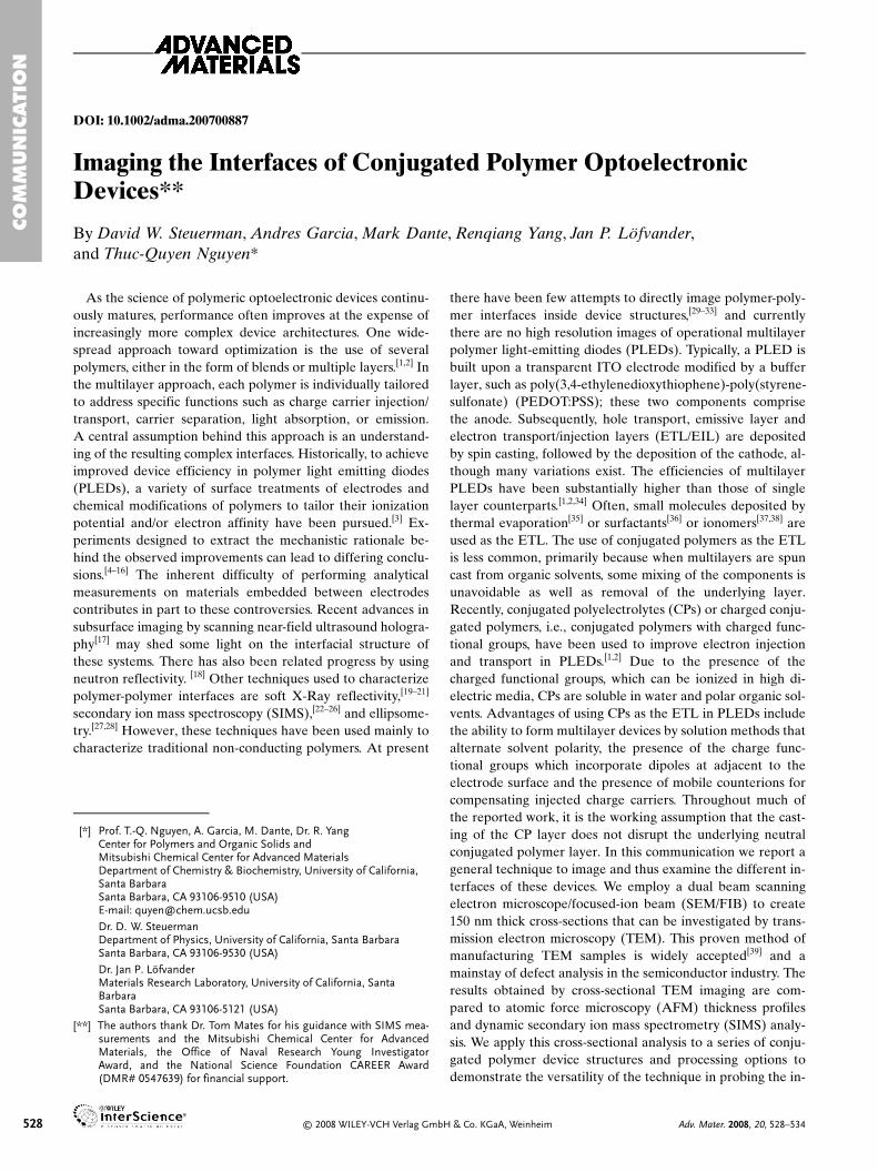
To fabricate a cross section, multilayer films or devices aretransferred to the e-beam evaporator for deposition of200 nm SiO2 to protect the organic layers from ion damageduring FIB processing, followed by a ∼ 3 nm sputter deposi-tion of Au to limit charging in the SEM. The cross-section fab-rication begins by locating the desired area in the SEM andwriting Pt alignment squares via FIB-assisted cleavage of aPt-organometallic vapor. The FIB (FEI Strata DB 235) is thenused to sculpt an “X” in each of the Pt squares (markers).These markers are used as references to ensure that the FIB
does not impinge on the final cross section area throughoutthe fabrication process. A thin Pt protective/supporting layeris then deposited over the fabrication area between themarkers. Next, the FIB is used to mill two large trenches oneither side of the cross-section that are repeatedly widenedand deepened using progressively smaller ion beam apertures.After each ion mill step, the alignment markers are re-imagedto account for any drift that may have occurred. Slowly thecross section between these trenches erodes until the only sep-aration is ∼ 150 nm thick. Midway through the trench crea-tion, the cross-section is nearly freed from the substrate bymilling along the bottom and sides. Upon completion, thecross-section is suspended above the substrate by two thintabs of Pt, as seen in Figure 1. In this geometry, the resultingsection (10 lm × 3 lm × 150 nm) can be readily removed by amicro-manipulated pulled glass rod and placed on a TEMgrid. These samples are subsequently imaged with a FEI Tec-nai G2 F30 microscope outfitted with a Gatan CCD camera.Stains and dyes were avoided to preserve the integrity of thenative device structure, albeit at the expense of contrast.
In this section we will discuss four multilayer devices. Twotypical PLED configurations using conjugated polyelectro-lytes are ITO/MEH-PPV(unannealed)/PFN+Br–/Al andITO/MEH-PPV(annealed)/PFN+Br–/Al. Two electron-onlydevices include, Al/MEH-PPV(unannealed)/PFP/Ba/Al and
CO
MM
UN
ICATIO
N
Adv. Mater. 2008, 20, 528–534 © 2008 WILEY-VCH Verlag GmbH & Co. KGaA, Weinheim www.advmat.de 529
Figure 1. Schematic composition of a multi-layer device as well as chemi-cal structures of polymers in this study. An SEM image of a device cross-section while still embedded in the substrate after the FIB process iscomplete. Note that this cross-section process can be performed at anyposition on the wafer with submicrometer precision.
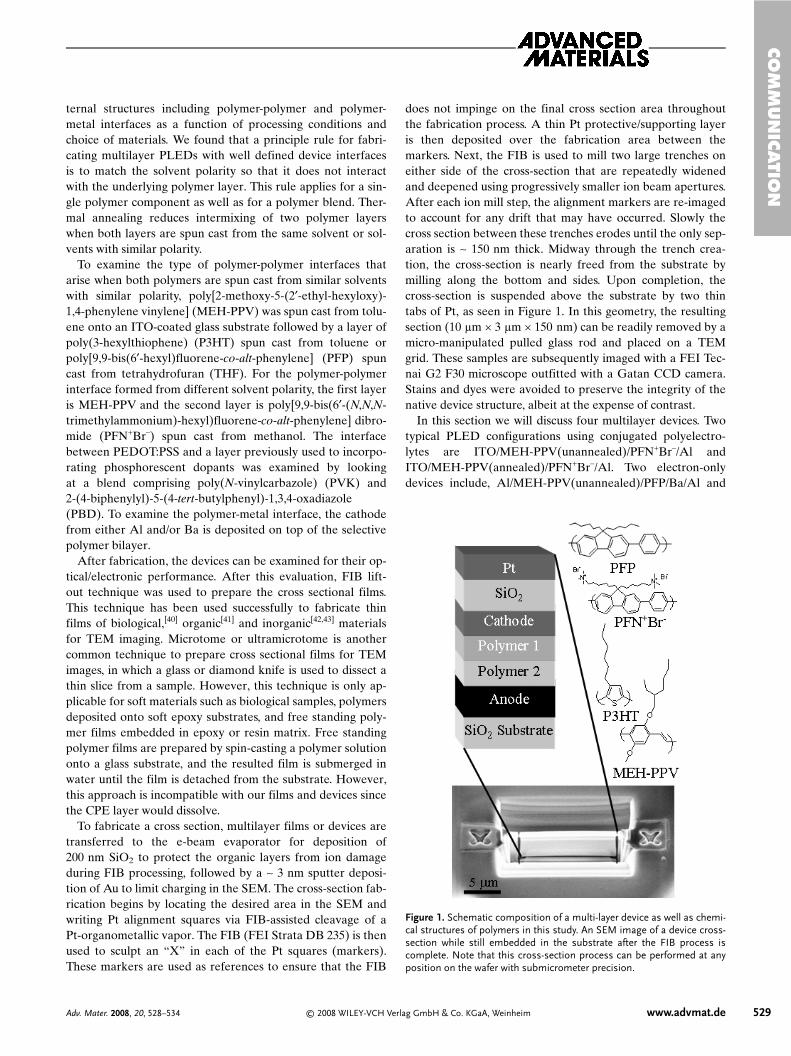
Al/MEH-PPV(annealed)/PFP/Ba/Al. Figure 2a shows the re-sulting TEM image from the ITO/MEH-PPV(unannealed)/PFN+Br–/Al device. The MEH-PPV(unannealed)/PFN+Br–
and PFN+Br–/Al interfaces are visible. Commensurate withAFM thickness measurements of single polymer layers((68 ± 2) nm for the MEH-PPV and (25 ± 3) nm for thePFN+Br–) and a bilayer ((96 ± 3) nm), we observe an interfacelocated (65 ± 2) nm above the ITO layer. As designed, theMEH-PPV(unannealed)/PFN+Br– interface between the neu-tral and charged polymers is well defined with little intermix-ing and dissolving of the underlying MEH-PPV layer. Tominimize intermixing of the two polymer layers, a poor sol-vent should be used to suppress dissolution of the underlyingpolymer. There should be little intermixing between theMEH-PPV and the PFN+Br– layers because MEH-PPV is notsoluble in methanol, even when heated. Furthermore, MEH-PPV is hydrophobic whereas PFN+Br– is hydrophilic; there-fore, there is no driving force for the two polymer layers tomix in solid state. Both polymers have a glass transition tem-perature above 100 °C. Additionally, it is evident that the con-trast is homogenous in each layer, indicating that there is nocompositional gradient, a signature of intermixing. If there ispartial dissolution of the underlying MEH-PPV layer uponthe deposition of the PFN+Br–, the total bilayer thicknesswould be much less than the sum of the single polymer layerthickness ((93 ± 4) nm). The total thickness estimated fromthe TEM image is (94 ± 2) nm, which agrees well with thethickness value obtained by the AFM measurements. Theseresults demonstrate that no shrinking or stretching of the sam-ple occurs during the cross section fabrication process. Thereis little contrast difference between the bulk of each polymer,which makes it difficult to assess the precise interfacial width.The interfacial region estimated from the TEM image is∼ 2 nm, which is in the agreement with the interfacial width(∼ 1.4 nm) obtained by soft X-Ray reflectivity measure-
ments.[44] The quantitative limits on the interfacial resolutionusing AFM and TEM are determined by the instrument reso-lutions: 0.1 Å for AFM vertical resolution and 0.25 nm forTEM lateral resolution. Any contrast is likely the result ofvariations in electron scattering due to differences in molecu-lar composition and/or polymer density. Since conjugatedpolymers consist of light atoms such as carbon, hydrogen, oxy-gen, and nitrogen, the scattering is weak, therefore, producespoor contrast. For our case, both conjugated polymers containcarbon and hydrogen. The MEH-PPV contains oxygenwhereas the PFN+Br– contains nitrogen and bromide ions.The electron density differences are small; therefore, the im-age contrast is weak. Staining polymer films with osmium tetr-oxide (OsO4), mercuric trifluoroacetate, ruthenium tetroxide(RuO4), phosphotungstic acid (PTA), hydrazine, etc. has beenshown to improve the image contrast.[45–47] However, staininghas been shown to introduce imaging artifacts.[48]
For our purposes, we define the area bounded by bulk poly-mer signature and crystalline cathode material as the poly-mer-cathode interface, i.e., PFN+Br–/Al, which in this case isapproximately 10 nm thick. This interface appears to havesome morphological structure at the nanometer scale, as indi-cated by parallel structures along the interface. This inter-facial region may also be a result of aluminum oxide forma-tion and/or the diffusion of Al atoms into the polymer layerduring the evaporation process.[49–51] TEM images obtainedfrom an ITO/MEH-PPV(annealed)/PFN+Br–/Al device ex-hibited no marked differences from those described forITO/MEH-PPV(unannealed)/PFN+Br–/Al (Fig. 2a).
Attempts to fabricate a multilayer device from unannealedMEH-PPV and PFP as an ETL, where both layers were spuncast from THF, led to transport characteristics consistent witha short circuited junction. This may be the result of multiplepin hole formation due to the complete removal of the neutralpolymer layer. Unfortunately, quantification of this phenome-non could not be pursued because all efforts to produce afunctioning diode were unsuccessful. Subsequent imaging ofthese devices verified that large areas of the anode and evapo-rated cathode were in intimate contact. It appears that onceMEH-PPV is cast, subsequent casting of PFP dissolves themajority of the pre-deposited polymer under our experimen-tal conditions. We will revisit neutral polymers cast on neutralpolymers later.
Figure 2b shows a TEM image of the Al/MEH-PPV(an-nealed)/PFP/Ba/Al. The PFP layer is spun from THF on ther-mally annealed MEH-PPV (220 °C for an hour) followed by aBa/Al (20 nm/100 nm as determined by quartz crystal micro-balance) cathode. The annealing process renders the MEH-PPV less soluble in organic solvents, thus allowing fabricationof a more robust bilayer device, although the reason for thelower solubility of the annealed MEH-PPV film remains un-known. The TEM image shows that the MEH-PPV/PFP inter-face varies smoothly from 2 to 15 nm along the length of thecross-section. We speculate that this could result from varia-tions in domain microstructure, but further analysis is neces-sary for confirmation. It is interesting to note that even
CO
MM
UN
ICATI
ON
530 www.advmat.de © 2008 WILEY-VCH Verlag GmbH & Co. KGaA, Weinheim Adv. Mater. 2008, 20, 528–534
Figure 2. Cross-sectional TEM images of polymer-bilayer devices fabri-cated with a FIB, showing a) unannealed MEH-PPV and PFN+Br– on ITOwith an Al top electrode. b) annealed MEH-PPV and PFP on Al with Ba/Altop electrode. This device was designed for electron only transport stud-ies. In both devices, the polymer-polymer interface can be found near thecenter and horizontally spanning the images. The observed position ofthese interfaces is consistent with thickness measurements of singlelayer structures performed via AFM. Observe that the Ba/PFP is rougherthan the Al/PFN+Br– interface. This was observed regardless of polymertype and can be attributed to the grain size and crystallinity of evaporatedBa versus Al.
though the bulk polymers show no contrast, yet the interfacecan be observed, possibly because of an interfacial dipole orcontact potential phenomenon. The PFP/Ba interface issignificantly rougher than that of the PFN+Br–/Al interface.The Ba/Al interface is clearly observed and the diffusion ofAl atoms into the Ba layer appears to be present.
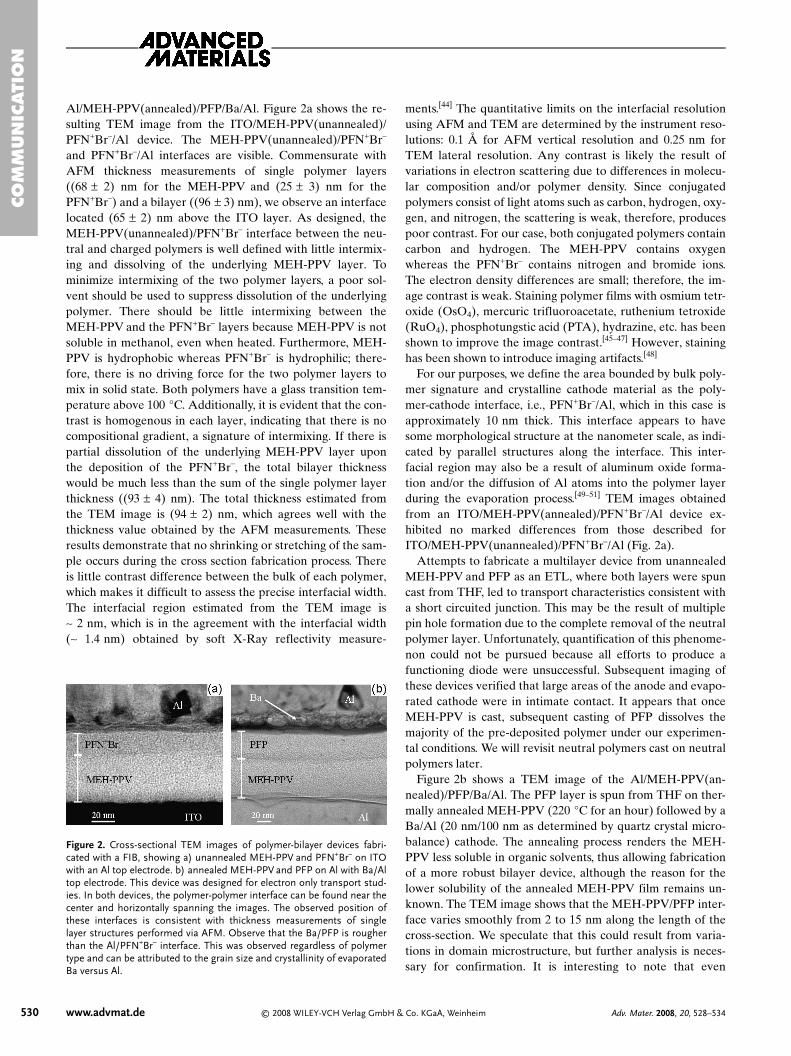
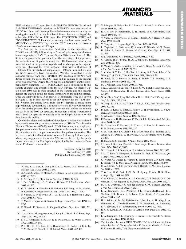
To further confirm that there is little intermixing or dissolu-tion of the MEH-PPV layer upon the deposition of thePFN+Br–, dynamic SIMS was performed on the ITO/MEH-PPV(unannealed)/PFN+Br–/Al devices. This technique hasbeen used to characterize various interfaces.[22–26] In SIMS, ahigh energy ion beam (Ga+, O2
+, or Cs+) is directed on thesample surface and the generated ions, atoms, clusters ofatoms, and molecular fragments are detected as a function oftime by the mass spectrometer, which is proportional to thedepth profile of the sample. Thus, this technique allows us toobserve the elemental composition as function of depth fromthe surface of the sample. SIMS can provide depth profileswith resolution down to a few nanometers and ppm sensitivity.As the surface of the device was etched away by the O2
+
beam, multiple fragments of various weights were monitoredsimultaneously. Since the conjugated polymers in this studycontain similar elements (largely composed of C, O, and H),determining the thickness of the individual constituents of thebilayers is quite challenging. However, it is possible for ourITO/MEH-PPV(unannealed)/PFN+Br–/Al device imaged inFigure 2a because the PFN+Br– contains the bromide counter-ions. Figure 3 shows the molecular compositional data fromthe ITO/MEH-PPV(unannealed)/PFN+Br–/Al device as afunction of the time that the ion beam is incident to thesurface. The removal of the Al top electrode is realized first.As the Al signal decays, the C and Br signals begin to increaseindicating the PFN+Br– layer is now being fragmented. The Brsignal is much lower than the C signal since there are two Brions and thirty C atoms per monomer. The Br signal drops sig-nificantly at ∼ 400 s whereas the C signal persists for another100 s. Eventually, In fragments are detected once the oxygenplasma reaches the depth of the ITO-coated glass substrate.Figure 3b plots the normalized fragment intensity for C andBr to examine the structure at the MEH-PPV and thePFN+Br– interface. This allows us to focus on the polymer-bi-layer where the first source of C (presumably from thePFN+Br–) is correlated with a large signal in the Br channel.At approximately midway through the C rich region of theSIMS spectrum, there is a shallow decrease in C amplitudeand ∼ 90 % drop in intensity of the Br signal. These two spec-tral characteristics taken together indicate that the C signalcomes from two separated polymer layers.[25] The aforemen-tioned spectral features are used to determine the thicknessesof the constituent polymer layers (PFN+Br–/MEH-PPV).[23]
To achieve this, first a crater was etched and the processstopped when the Al signal dropped and the C signal in-creased. Next, a second crater was etched and the etching wasstopped when the Br signal started decreasing. For the finaletch we created a third crater that was stopped at the begin-ning of the In signal. Finally, a profilometer was used to deter-
mine the depth of all three craters which in turn reveal thethicknesses of the two polymer layers. From the SIMS and theprofilometry measurements, the PFN+Br– and the MEH-PPVlayer thicknesses are (22 ± 3) nm and (58 ± 5) nm, respective-ly. These thicknesses agree with the results obtained from theAFM and the cross sectional TEM image analysis. Thus, theSIMS spectral signatures support the distinct partitioning ofthe constituents of the polymer-bilayer observed in the TEManalysis.
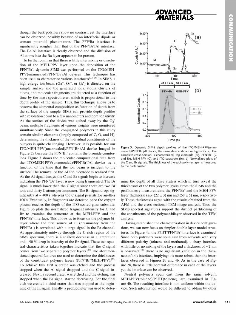
Having established the characterization in device configura-tions, we can now focus on simpler double layer model struc-tures. In Figure 4a, the P3HT/PFN+Br– interface is examined.Since both polymers were spun cast from solvents with verydifferent polarity (toluene and methanol), a sharp interfacewith little or no mixing of the layers and a thickness of ∼ 2 nmis observed.[44] There is no significant variation in the thick-ness of this interface, implying it is more robust than the inter-faces observed in Figures 2b and 4b. As in the case of Fig-ure 2b, there is little contrast difference in each of the layers,yet the interface can be observed.
Neutral polymers spun cast from the same solvent,MEH-PPV(toluene)/P3HT(toluene), are examined in Fig-ure 4b. The resulting interface is non uniform within the de-vice. Such information would be difficult to obtain by other
CO
MM
UN
ICATIO
N
Adv. Mater. 2008, 20, 528–534 © 2008 WILEY-VCH Verlag GmbH & Co. KGaA, Weinheim www.advmat.de 531
300 400 5000
1x10⁵
2x10⁵
3x10⁵
4x10⁵
Time
Br
In
C
Co
un
ts (
A.U
.)
Al
300 400 500
0.0
0.2
0.4
0.6
0.8
1.0
No
rma
lize
d C
ou
nts
Time (s)
C
Br
22 ± 3 nm 58 ± 5 nm
300 400 5000
1x10⁵
2x10⁵
3x10⁵
4x10⁵
Time
Br
In
C
Co
un
ts (
A.U
.)
Al
300 400 500
0.0
0.2
0.4
0.6
0.8
1.0
No
rma
lize
d C
ou
nts
Time (s)
C
Br
PFN+Br MEH-PPV
22 ± 3 nm
PFN+Br MEH-PPV
58 ± 5 nm
(a)
(b)
Figure 3. Dynamic SIMS depth profiles of the ITO/MEH-PPV(unan-nealed)/PFN+Br–/Al device, the same device shown in Figure 2a. a) Thecomplete cross-section is characterized: top electrode (Al), PFN+Br– (Cand Br), MEH-PPV (C), and ITO substrate (In). b) Normalized plots ofthe C and Br signals. The thickness of the each polymer layer is measuredby the profilometer.
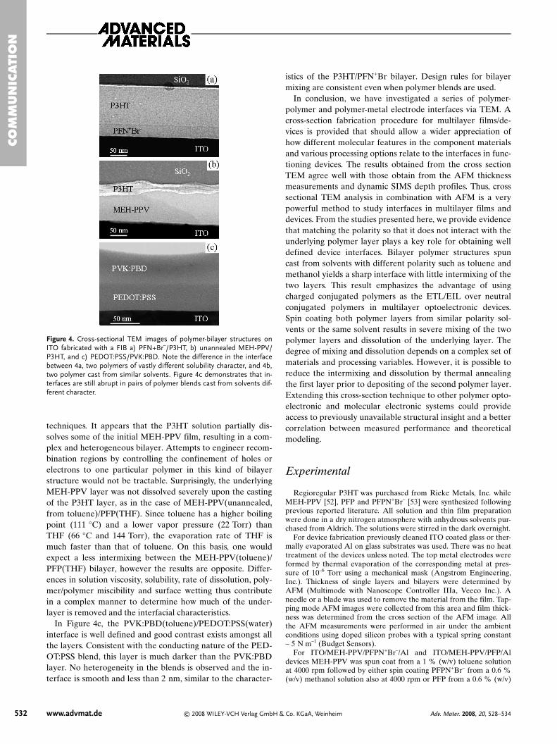
techniques. It appears that the P3HT solution partially dis-solves some of the initial MEH-PPV film, resulting in a com-plex and heterogeneous bilayer. Attempts to engineer recom-bination regions by controlling the confinement of holes orelectrons to one particular polymer in this kind of bilayerstructure would not be tractable. Surprisingly, the underlyingMEH-PPV layer was not dissolved severely upon the castingof the P3HT layer, as in the case of MEH-PPV(unannealed,from toluene)/PFP(THF). Since toluene has a higher boilingpoint (111 °C) and a lower vapor pressure (22 Torr) thanTHF (66 °C and 144 Torr), the evaporation rate of THF ismuch faster than that of toluene. On this basis, one wouldexpect a less intermixing between the MEH-PPV(toluene)/PFP(THF) bilayer, however the results are opposite. Differ-ences in solution viscosity, solubility, rate of dissolution, poly-mer/polymer miscibility and surface wetting thus contributein a complex manner to determine how much of the under-layer is removed and the interfacial characteristics.
In Figure 4c, the PVK:PBD(toluene)/PEDOT:PSS(water)interface is well defined and good contrast exists amongst allthe layers. Consistent with the conducting nature of the PED-OT:PSS blend, this layer is much darker than the PVK:PBDlayer. No heterogeneity in the blends is observed and the in-terface is smooth and less than 2 nm, similar to the character-
istics of the P3HT/PFN+Br bilayer. Design rules for bilayermixing are consistent even when polymer blends are used.
In conclusion, we have investigated a series of polymer-polymer and polymer-metal electrode interfaces via TEM. Across-section fabrication procedure for multilayer films/de-vices is provided that should allow a wider appreciation ofhow different molecular features in the component materialsand various processing options relate to the interfaces in func-tioning devices. The results obtained from the cross sectionTEM agree well with those obtain from the AFM thicknessmeasurements and dynamic SIMS depth profiles. Thus, crosssectional TEM analysis in combination with AFM is a verypowerful method to study interfaces in multilayer films anddevices. From the studies presented here, we provide evidencethat matching the polarity so that it does not interact with theunderlying polymer layer plays a key role for obtaining welldefined device interfaces. Bilayer polymer structures spuncast from solvents with different polarity such as toluene andmethanol yields a sharp interface with little intermixing of thetwo layers. This result emphasizes the advantage of usingcharged conjugated polymers as the ETL/EIL over neutralconjugated polymers in multilayer optoelectronic devices.Spin coating both polymer layers from similar polarity sol-vents or the same solvent results in severe mixing of the twopolymer layers and dissolution of the underlying layer. Thedegree of mixing and dissolution depends on a complex set ofmaterials and processing variables. However, it is possible toreduce the intermixing and dissolution by thermal annealingthe first layer prior to depositing of the second polymer layer.Extending this cross-section technique to other polymer opto-electronic and molecular electronic systems could provideaccess to previously unavailable structural insight and a bettercorrelation between measured performance and theoreticalmodeling.
Experimental
Regioregular P3HT was purchased from Rieke Metals, Inc. whileMEH-PPV [52], PFP and PFPN+Br– [53] were synthesized followingprevious reported literature. All solution and thin film preparationwere done in a dry nitrogen atmosphere with anhydrous solvents pur-chased from Aldrich. The solutions were stirred in the dark overnight.
For device fabrication previously cleaned ITO coated glass or ther-mally evaporated Al on glass substrates was used. There was no heattreatment of the devices unless noted. The top metal electrodes wereformed by thermal evaporation of the corresponding metal at pres-sure of 10–6 Torr using a mechanical mask (Angstrom Engineering,Inc.). Thickness of single layers and bilayers were determined byAFM (Multimode with Nanoscope Controller IIIa, Veeco Inc.). Aneedle or a blade was used to remove the material from the film. Tap-ping mode AFM images were collected from this area and film thick-ness was determined from the cross section of the AFM image. Allthe AFM measurements were performed in air under the ambientconditions using doped silicon probes with a typical spring constant∼ 5 N m–1 (Budget Sensors).
For ITO/MEH-PPV/PFPN+Br–/Al and ITO/MEH-PPV/PFP/Aldevices MEH-PPV was spun coat from a 1 % (w/v) toluene solutionat 4000 rpm followed by either spin coating PFPN+Br– from a 0.6 %(w/v) methanol solution also at 4000 rpm or PFP from a 0.6 % (w/v)
CO
MM
UN
ICATI
ON
532 www.advmat.de © 2008 WILEY-VCH Verlag GmbH & Co. KGaA, Weinheim Adv. Mater. 2008, 20, 528–534
Figure 4. Cross-sectional TEM images of polymer-bilayer structures onITO fabricated with a FIB a) PFN+Br–/P3HT, b) unannealed MEH-PPV/P3HT, and c) PEDOT:PSS/PVK:PBD. Note the difference in the interfacebetween 4a, two polymers of vastly different solubility character, and 4b,two polymer cast from similar solvents. Figure 4c demonstrates that in-terfaces are still abrupt in pairs of polymer blends cast from solvents dif-ferent character.
THF solution at 1500 rpm. For Al/MEH-PPV/ PFPN+Br–/Ba/Al andAl/MEH-PPV/PFP/Ba/Al devices the MEH-PPV layer was heated at220 °C for 1 hour and then rapidly cooled to room temperature by re-moving the sample from the hotplate followed by spin coating of theeither the PFPN+Br– or PFP layer. For ITO/PFPN+Br–/P3HT andITO/MEH-PPV/P3HT identical processing condition were used forMEH-PPV and PFPN+Br– layers while P3HT was spun coat from a1%w/v toluene solution at 1500 rpm.
The first step in cross section fabrication is the deposition of200–300 nm of SiO2 followed by ∼ 3 nm of gold using an electronbeam evaporator (10 kV Temescal Series 260 e-beam Source). TheSiO2 layer protects the polymer from the next stage of the process,the deposition of Pt patterns using the FIB. However, these layerswere not used in the previous reports and no damage to the organiclayer was observed for cross sectional films with a thickness of∼ 100 nm. For our study, all samples are ∼ 150 nm thick and we alsouse SiO2 protective layer for caution. We also fabricated a crosssectional sample from the ITO/MEH-PPV(unannealed)/PFN+Br–/Aldevice without the use of the SiO2 layer and no damage to the organiclayer was observed. During the Pt deposition, trimethyl-methylcyclo-pentadienyl-platinum ((CH3)3(CH3C5H9Pt) gas is introduced to thesample chamber and absorbs onto the SiO2 surface. An intense Ga+
ion beam (500 pA) is then directed at the sample and the organicligands are ejected in the gas phase leaving Pt on the sample surface.Once the sample is tilted to an angle of 7° and nearly freed as is shownin Figure 1, the Pt layer serves as the only support for the TEM sam-ple. Notches are etched away from the Pt supports to make themapproximately 100 nm thick. This facilitates easy lift out of the sampleafter the cutting process. The initial trenches that define the sampleare cut with the 5000 pA aperture. Subsequent etching is performedwith a 1000 pA aperture eventually with the 300 pA aperture for thefinal fine-scale milling.
Qualitative elemental analysis of the polymer devices was achievedby dynamic secondary ion mass spectrometry (SIMS). To this end aPhysical Electronics 6650 Dynamic SIMS instrument was employed.Samples were etched by an oxygen plasma with a nominal current of38 pA while an electron gun was used for charged compensation. Theactive etch area for all measurements was a 150 lm by 150 lm squarewhere only fragments of the center 20% were collected by the quad-rupolar mass detector. For depth analysis of individual craters, a Dek-tak VI Profilometer was utilized.
Received: April 14, 2007Revised: July 17, 2007
Published online: January 9, 2008
–[1] W. Ma, P. K. Iyer, X. Gong, B. Liu, D. Moses, G. C. Bazan, A. J.
Heeger, Adv. Mater. 2005, 17, 274.[2] X. Gong, S. Wang, D. Moses, G. C. Bazan, A. J. Heeger, Adv. Mater.
2005, 17, 2053.[3] L. S. Hung, C. H. Chen, Mater. Sci. Eng. R 2002, 39, 143.[4] J. Cui, Q. Huang, J. G. C. Veinot, H. Yan, T. J. Marks, Adv. Mater.
2002, 14, 565.[5] G. E. Jabbour, Y. Kawabe, S. E. Shaheen, J. F. Wang, M. M. Morrell,
B. Kippelen, N. Peyghamarian, Appl. Phys. Lett. 1997, 71, 1762.[6] F. Nüesch, E. W. Forsythe, Q. T. Le, Y. Gao, L. J. Rothberg, J. Appl.
Phys. 2000, 87, 7973.[7] T. Mori, H. Fujikawa, S. Tokito, T. Taga, Appl. Phys. Lett. 1998, 73,
2763.[8] F. Nüesch, K. Kamaras, L. Zuppiroli, Chem. Phys. Lett. 1998, 283,
194.[9] S. A. Carter, M. Angelopoulos, S. Karg, P. J. Brock, J. C. Scott, Appl.
Phys. Lett. 1997, 70, 2067.[10] S. F. J. Appleyard, S. R. Day, R. D. Pickford, M. R. Willis, J. Mater.
Chem. 2000, 10, 169.[11] P. K. H. Ho, J.-S. Kim, J. H. Burroughes, H. Becker, S. F. Y. Li,
T. M. Brown, F. Cacialli, R. H. Friend, Nature 2000, 404, 481.
[12] V. Bliznyuk, B. Ruhstaller, P. J. Brock, U. Scherf, S. A. Carter, Adv.Mater. 1999, 11, 1257.
[13] P. K. H. Ho, M. Granstrom, R. H. Friend, N. C. Greenham, Adv.Mater. 1998, 10, 769.
[14] Y. Yang, E. Westerweele, C. Zahng, P. Smith, A. J. Heeger, J. Appl.Phys. 1995, 77, 694.
[15] Y. Yang, A. H. Heeger, Appl. Phys. Lett. 1993, 64, 1245.[16] L. Zuppiroli, L. Si-Ahmed, K. Kamars, F. Nüesch, M. N. Bussas,
D. Ades, A. Siove, E. Moons, M. Grätzel, Eur. Phys. J. B 1999,11, 505.
[17] G. S. Shekhawat, V. P. Dravid, Science 2005, 310, 89.[18] C. Carelli, R. N. Young, R. A. L. Jones, M. Sferrazza, Europhys.
Lett. 2006, 75, 274.[19] C. Wang, T. Araki, B. Watts, S. Harton, T. Koga, S. Basu, H. Ade,
J. Vac. Sci. Technol. A 2007, 25, 575.[20] S. Y. Kim, S. Y. Ryu, J. M. Choi, S. J. Kang, S. P. Park, S. Im, C. N.
Whang, D. S. Choib, Thin Solid Films 2001, 398–399, 78.[21] H. Kima, M. D. Fostera, H. Jiang, S. Tullisb, T. J. Bunning, C. F.
Majkrzak, Polymer 2004, 45, 3175.[22] M. S. Wagner, Anal. Chem. 2005, 77, 911.[23] J. K. J. Van Duren, X. Yang, J. Loos, C. W. T. Bulle-Lieuwma, A. B.
Sieval, J. C. Hummelen, R. A. J. Janssen, Adv. Funct. Mater. 2004,14, 425.
[24] W.-Y. Chen, Y.-C. Ling, B.-J. Chen, H.-H. Shih, C.-H. Cheng, Appl.Surf. Sci. 2006, 252, 6594.
[25] W. Song, Z. Li, S. K. So, Y. Qiu, Y. Zhu, L. Cao, Surf. Interface Anal.2001, 32, 102.
[26] B. Kim, H. Kang, K. Char, K. Katsov, G. H. Fredrickson, E. J. Kra-mer, Macromolecules 2005, 38, 6108.
[27] S. Yukioka, T. Inoue, Polymer 1993, 34, 1256.[28] P. Duckworth, H. Richardson, C. Carelli, J. L. Keddie, Surf. Interface
Anal. 2004, 36, 33.[29] M. Granstrom, K. Petritsch, A. C. Arias, A. Lux, M. R. Andersson,
R. H. Friend, Nature 1998, 395, 257.[30] C. M. Ramsdale, I. C. Bache, J. D. MacKenzie, D. S. Thomas, A. C.
Arias, A. M. Donald, R. H. Friend, N. C. Greenham, Phys. E 2002,14, 268.
[31] H. Hoppe, N. S. Sariciftci, J. Mater. Chem. 2006, 16, 45.[32] J. Loosa, J. K. J. van Durenb, F. Morrisseyc, R. A. J. Janssen, Thin
Solid Films 2002, 43, 7493.[33] W. U. Huynh, J. J. Dittmer, A. P. Alivisatos, Science 2002, 295, 2425.[34] J. Li, T. Sano, Y. Hirayama, T. Tomita, H. Fujii, K. Wakisaka, Jpn.
J. Appl. Phys. 2006, 45, 3746.[35] G. Wantz, O. Dautel, L. Vignau, F. Serein-Spirau, J. P. Lere-Porte,
L. Hirsch, J. J. E. Moreau, J. P. Parneix, Synth. Met. 2006, 156, 690.[36] C. A. Olivati, A. J. F. Carvalho, D. T. Balogh, R. M. Faria, J. Mater.
Sci. 2006, 41, 2767.[37] T. W. Lee, O. O. Park, L. M. Do, T. Zyung, T. Ahn, H. K. Shim,
J. Appl. Phys. 2001, 90, 2128.[38] C. A. Olivati, M. Ferreira, A. J. F. Carvalho, D. T. Balogh, O. N. Oli-
veira, Jr., H. von Seggern, R. M. Faria, Chem. Phys. Lett. 2005, 408, 31.[39] M. H. F. Overwijk, F. C. van den Heuvel, C. W. T. Bulle-Lieuwma,
J. Vac. Sci. Technol. B 1993, 11, 2021.[40] L. A. Giannuzzi, B. I. Prenitzer, J. L. Drown-MacDonald, T. L.
Shofner, S. R. Brown, R. B. Irwin, F. A. Stevie, J. Process Anal.Chem. 1999, 4, 162.
[41] H. J. White, Y. Pu, M. Rafailovich, J. Sokolov, A. H. King, L. A.Giannuzzi, C. Urbanik-Shannon, B. W. Kempshall, A. Eisenberg,S. A. Schwarz, Y. M. Strzhemechny, Polymer 2001, 42, 1613.
[42] E. C. G. Kirk, D. A. Williams, H. Ahmed, Inst. Phys. Ser. 1989, 100,501.
[43] L. A. Giannuzzi, J. L. Drown, S. R. Brown, R. B. Irwin, F. A. Stevie,Microsc. Res. Tech. 1998, 41, 285.
[44] The interface between MEH-PPV/PFN+Br– is ∼ 1.4 nm as deter-mined by the soft X-ray reflectivity. K. Sohn, A. Garcia, G. Bazan,E. Kramer, H. Aide, T.-Q. Nguyen, unpublished.
CO
MM
UN
ICATIO
N
Adv. Mater. 2008, 20, 528–534 © 2008 WILEY-VCH Verlag GmbH & Co. KGaA, Weinheim www.advmat.de 533

[45] Z. Yin, J. Yang, N. Coombs, M. A. Winnik, R. A. Ryntz, P. V. Yaneff,Polymer 2007, 48, 1297.
[46] J. S. Trent, J. I. Scheinbeim, P. R. Couchman, J. Polym. Sci. Polym.Lett. Ed. 1981, 19, 315.
[47] R. J. Spontak, M. C. Williams, D. A. Agard, Macromolecules 1988,21, 1377.
[48] T. M. Chou, P. Prayoonthong, A. Aitouchen, M. Libera, Polymer2002, 43, 2085.
[49] F. Faupel, R. Willecke, A. Thran, Mater. Sci. Eng. R 1998, 22, 1.[50] Y. Hirose, A. Kahn, V. Aristov, P. Soukiassian, V. Bulovic, S. R. For-
rest, Phys. Rev. B 1996, 54, 13748.[51] G. Parthasarathy, C. Shen, A. Kahn, S. R. Forrest, J. Appl. Phys.
2001, 89, 4986.[52] C. J. Neef, J. P. Ferraris, Macromolecules 2000, 33, 2311.[53] M. Stork, B. S. Gaylord, A. J. Heeger, G. C. Bazan, Adv. Mater.
2002, 14, 361.
______________________
CO
MM
UN
ICATI
ON
534 www.advmat.de © 2008 WILEY-VCH Verlag GmbH & Co. KGaA, Weinheim Adv. Mater. 2008, 20, 528–534