ieee sf bay area mems &...
TRANSCRIPT
IEEE SF Bay Area MEMS & Sensors
http://sites.ieee.org/scv-mems/
October 22, 2014

Meeting Sponsor
Acuity IncorporatedFremont, CA, USA
www.acuitymicro.com
Complimentary food and refreshments sponsored by Acuity Inc.
Thanks to Dr. Jim Knutti, President/CEO
2
Upcoming Meetings
Nov. 19th, 2014 (Wednesday) 7:45 PM to 8:45 PM.Title: Innovative Pressure Sensing Solutions.Speaker: Mr. Holger Doering, Chief Operating Officer, Silicon Microstructures, Inc.Location: Qualcomm, Building B, Room 132, 3165 Kifer Road, Santa Clara, CA.Food: Pizza and beverages will be available starting at 7:15 pm for a $5 donationat the door.
Feb. 25th, 2015 (Wednesday) 7:45 PM to 8:45 PM.Title: Building Successful MEMS Company: From Start to IPOSpeaker: Mr. Steve Nasiri, Nasiri Ventures.Location: TBD
Mar. 25th, 2015 (Wednesday) 5:30 PM to 7:30 PM.IEEE MEMS and Sensors Happy HourLocation: TBD
3
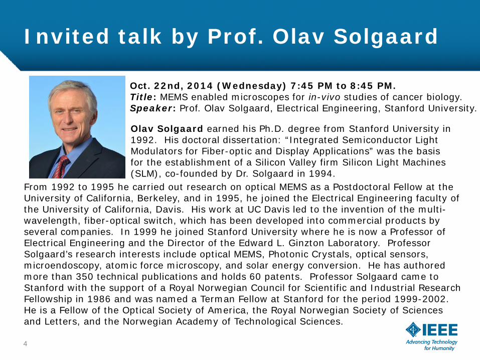
Invited talk by Prof. Olav Solgaard
From 1992 to 1995 he carried out research on optical MEMS as a Postdoctoral Fellow at the University of California, Berkeley, and in 1995, he joined the Electrical Engineering faculty of the University of California, Davis. His work at UC Davis led to the invention of the multi-wavelength, fiber-optical switch, which has been developed into commercial products by several companies. In 1999 he joined Stanford University where he is now a Professor of Electrical Engineering and the Director of the Edward L. Ginzton Laboratory. Professor Solgaard’s research interests include optical MEMS, Photonic Crystals, optical sensors, microendoscopy, atomic force microscopy, and solar energy conversion. He has authored more than 350 technical publications and holds 60 patents. Professor Solgaard came to Stanford with the support of a Royal Norwegian Council for Scientific and Industrial Research Fellowship in 1986 and was named a Terman Fellow at Stanford for the period 1999-2002. He is a Fellow of the Optical Society of America, the Royal Norwegian Society of Sciences and Letters, and the Norwegian Academy of Technological Sciences.
Oct. 22nd, 2014 (Wednesday) 7:45 PM to 8:45 PM.Title: MEMS enabled microscopes for in-vivo studies of cancer biology.Speaker: Prof. Olav Solgaard, Electrical Engineering, Stanford University.
Olav Solgaard earned his Ph.D. degree from Stanford University in 1992. His doctoral dissertation: “Integrated Semiconductor Light Modulators for Fiber-optic and Display Applications” was the basis for the establishment of a Silicon Valley firm Silicon Light Machines (SLM), co-founded by Dr. Solgaard in 1994.
4
1
Solgaard Lab, Stanford
Acknowledgements: J.-W. Jeung, H. Ra, C. Jan, A. Gellineau, M. Mandela, C. Contag
Support: Boeing, CIS, CPN, DARPA, NIH, NSF
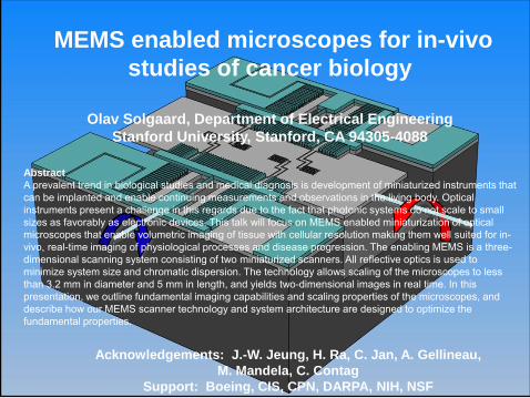
MEMS enabled microscopes for in-vivo studies of cancer biology
Olav Solgaard, Department of Electrical EngineeringStanford University, Stanford, CA 94305-4088
AbstractA prevalent trend in biological studies and medical diagnosis is development of miniaturized instruments that can be implanted and enable continuing measurements and observations in the living body. Optical instruments present a challenge in this regards due to the fact that photonic systems do not scale to small sizes as favorably as electronic devices. This talk will focus on MEMS enabled miniaturization of optical microscopes that enable volumetric imaging of tissue with cellular resolution making them well suited for in-vivo, real-time imaging of physiological processes and disease progression. The enabling MEMS is a three-dimensional scanning system consisting of two miniaturized scanners. All reflective optics is used to minimize system size and chromatic dispersion. The technology allows scaling of the microscopes to less than 3.2 mm in diameter and 5 mm in length, and yields two-dimensional images in real time. In this presentation, we outline fundamental imaging capabilities and scaling properties of the microscopes, and describe how our MEMS scanner technology and system architecture are designed to optimize the fundamental properties.
Solgaard Lab, Stanford
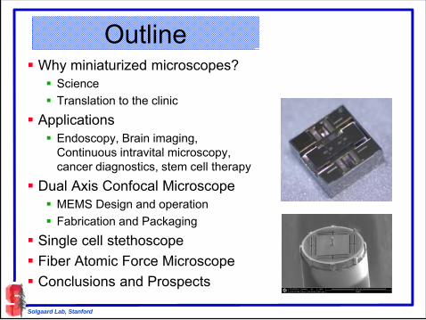
Outline Why miniaturized microscopes? Science
Translation to the clinic
Applications Endoscopy, Brain imaging,
Continuous intravital microscopy, cancer diagnostics, stem cell therapy
Dual Axis Confocal Microscope MEMS Design and operation
Fabrication and Packaging
Single cell stethoscope
Fiber Atomic Force Microscope
Conclusions and Prospects
1
Solgaard Lab, Stanford
Acknowledgements: J.-W. Jeung, H. Ra, C. Jan, A. Gellineau, M. Mandela, C. Contag
Support: Boeing, CIS, CPN, DARPA, NIH, NSF
MEMS enabled microscopes for in-vivo studies of cancer biology
Olav Solgaard, Department of Electrical EngineeringStanford University, Stanford, CA 94305-4088
AbstractA prevalent trend in biological studies and medical diagnosis is development of miniaturized instruments that can be implanted and enable continuing measurements and observations in the living body. Optical instruments present a challenge in this regards due to the fact that photonic systems do not scale to small sizes as favorably as electronic devices. This talk will focus on MEMS enabled miniaturization of optical microscopes that enable volumetric imaging of tissue with cellular resolution making them well suited for in-vivo, real-time imaging of physiological processes and disease progression. The enabling MEMS is a three-dimensional scanning system consisting of two miniaturized scanners. All reflective optics is used to minimize system size and chromatic dispersion. The technology allows scaling of the microscopes to less than 3.2 mm in diameter and 5 mm in length, and yields two-dimensional images in real time. In this presentation, we outline fundamental imaging capabilities and scaling properties of the microscopes, and describe how our MEMS scanner technology and system architecture are designed to optimize the fundamental properties.
Solgaard Lab, Stanford
Outline Why miniaturized microscopes? Science
Translation to the clinic
Applications Endoscopy, Brain imaging,
Continuous intravital microscopy, cancer diagnostics, stem cell therapy
Dual Axis Confocal Microscope MEMS Design and operation
Fabrication and Packaging
Single cell stethoscope
Fiber Atomic Force Microscope
Conclusions and Prospects
2
Solgaard Lab, Stanford
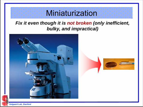
MiniaturizationFix it even though it is not broken (only inefficient,
bulky, and impractical)
10 cm
Solgaard Lab, Stanford
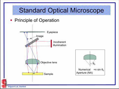
Standard Optical Microscope
Principle of Operation
Eyepiece
Incoherentillumination
Objective lens
Sample
Image
θ0
NumericalAperture (NA)
=n sin θ0
2
Solgaard Lab, Stanford
MiniaturizationFix it even though it is not broken (only inefficient,
bulky, and impractical)
10 cm
Solgaard Lab, Stanford
Standard Optical Microscope
Principle of Operation
Eyepiece
Incoherentillumination
Objective lens
Sample
Image
θ0
NumericalAperture (NA)
=n sin θ0
3
Solgaard Lab, Stanford
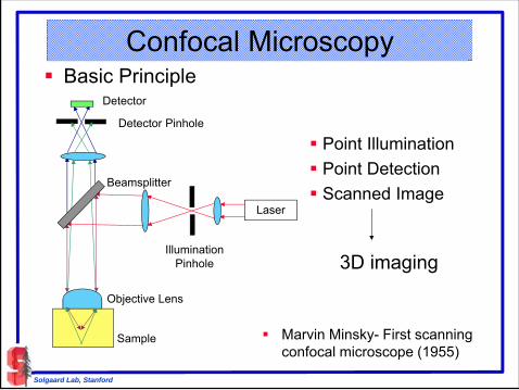
Confocal Microscopy Basic Principle
Laser
Detector
Detector Pinhole
IlluminationPinhole
Objective Lens
Sample
Beamsplitter
Point Illumination
Point Detection
Scanned Image
3D imaging
Marvin Minsky- First scanning confocal microscope (1955)
Solgaard Lab, Stanford
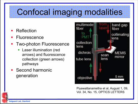
Confocal imaging modalities
Reflection
Fluorescence
Two-photon Fluorescence Laser illumination (red
arrows) and fluorescence collection (green arrows) pathways
Second harmonic generation
Piyawattanametha et al, August 1, 09, Vol. 34, No. 15, OPTICS LETTERS
3
Solgaard Lab, Stanford
Confocal Microscopy Basic Principle
Laser
Detector
Detector Pinhole
IlluminationPinhole
Objective Lens
Sample
Beamsplitter
Point Illumination
Point Detection
Scanned Image
3D imaging
Marvin Minsky- First scanning confocal microscope (1955)
Solgaard Lab, Stanford
Confocal imaging modalities
Reflection
Fluorescence
Two-photon Fluorescence Laser illumination (red
arrows) and fluorescence collection (green arrows) pathways
Second harmonic generation
Piyawattanametha et al, August 1, 09, Vol. 34, No. 15, OPTICS LETTERS
4
Solgaard Lab, Stanford
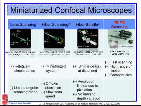
Lens Scanning1 Fiber Scanning2 Fiber Bundle3 MEMS Scanning
(+) Relatively simple optics
(+) Miniaturized system
(+) Simple design at distal end
(+) Fast scanning(+) High range of
motion(+) Compact size
(-) Limited angular scanning range
(-) Off-axis aberration
(-) Slow scan speed
(-) Resolution limited due to pixelation
(-) No imaging depth variation
Miniaturized Confocal Microscopes
Sung, et al., Optics Express, 2003Thiberville, et al., PATS, 2009
Dikensheets and Kino, Optics Letters, 1996
Giniunas, et al., Electron. Lett, 1991Dikensheets, et al., SPIE 1994
Harris, US patent # 5,120,953, 1992Dabbs, et al., Applied Optics, 1992
1-D MEMS scanners
1 – 3. Images from B.A. Flusberg, et al, Nature Methods, Vol. 2, No. 12, 2005
Solgaard Lab, Stanford
Dual Axis Confocal (DAC) Microscope
HL: hemispherical lens PMT: photomultiplier tube
Advantages of the DAC: Larger dynamic range – deeper imaging Low NA objective lens – miniaturization Longer working distance – post-objective scanning Cellular resolution in both transverse and axial dimensions

4
Solgaard Lab, Stanford
Lens Scanning1 Fiber Scanning2 Fiber Bundle3 MEMS Scanning
(+) Relatively simple optics
(+) Miniaturized system
(+) Simple design at distal end
(+) Fast scanning(+) High range of
motion(+) Compact size
(-) Limited angular scanning range
(-) Off-axis aberration
(-) Slow scan speed
(-) Resolution limited due to pixelation
(-) No imaging depth variation
Miniaturized Confocal Microscopes
Sung, et al., Optics Express, 2003Thiberville, et al., PATS, 2009
Dikensheets and Kino, Optics Letters, 1996
Giniunas, et al., Electron. Lett, 1991Dikensheets, et al., SPIE 1994
Harris, US patent # 5,120,953, 1992Dabbs, et al., Applied Optics, 1992
1-D MEMS scanners
1 – 3. Images from B.A. Flusberg, et al, Nature Methods, Vol. 2, No. 12, 2005
Solgaard Lab, Stanford
Dual Axis Confocal (DAC) Microscope
HL: hemispherical lens PMT: photomultiplier tube
Advantages of the DAC: Larger dynamic range – deeper imaging Low NA objective lens – miniaturization Longer working distance – post-objective scanning Cellular resolution in both transverse and axial dimensions
5
Solgaard Lab, Stanford
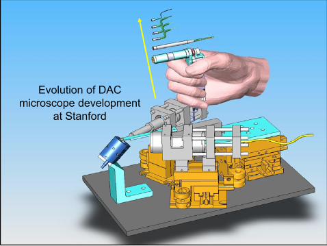
Evolution of DAC microscope development
at Stanford
Solgaard Lab, Stanford
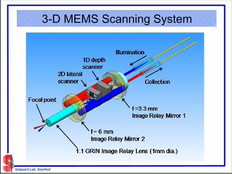
3-D MEMS Scanning System
5
Solgaard Lab, Stanford
Evolution of DAC microscope development
at Stanford
Solgaard Lab, Stanford
3-D MEMS Scanning System
6
Solgaard Lab, Stanford
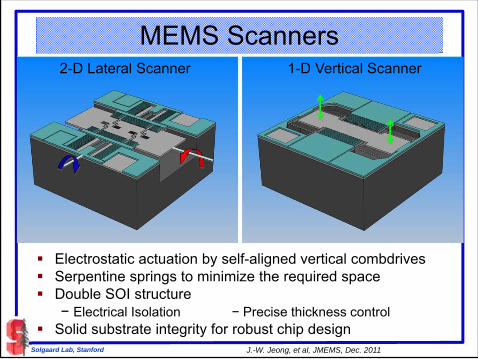
MEMS Scanners
Electrostatic actuation by self-aligned vertical combdrives Serpentine springs to minimize the required space Double SOI structure
− Electrical Isolation − Precise thickness control Solid substrate integrity for robust chip design
2-D Lateral Scanner 1-D Vertical Scanner
J.-W. Jeong, et al, JMEMS, Dec. 2011
Solgaard Lab, Stanford
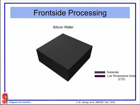
Frontside Processing
J.-W. Jeong, et al, JMEMS, Dec. 2011
SubstrateLow Temperature Oxide
(LTO)
Silicon Wafer
6
Solgaard Lab, Stanford
MEMS Scanners
Electrostatic actuation by self-aligned vertical combdrives Serpentine springs to minimize the required space Double SOI structure
− Electrical Isolation − Precise thickness control Solid substrate integrity for robust chip design
2-D Lateral Scanner 1-D Vertical Scanner
J.-W. Jeong, et al, JMEMS, Dec. 2011
Solgaard Lab, Stanford
Frontside Processing
J.-W. Jeong, et al, JMEMS, Dec. 2011
SubstrateLow Temperature Oxide
(LTO)
Silicon Wafer
7
Solgaard Lab, Stanford
Frontside Processing
SubstrateLow Temperature Oxide
(LTO)
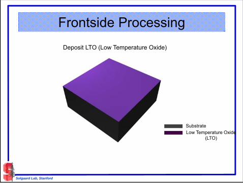
Deposit LTO (Low Temperature Oxide)
Solgaard Lab, Stanford
Frontside Processing
SubstrateLow Temperature Oxide
(LTO)
Pattern LTO to define a large cavity (Mask 1)
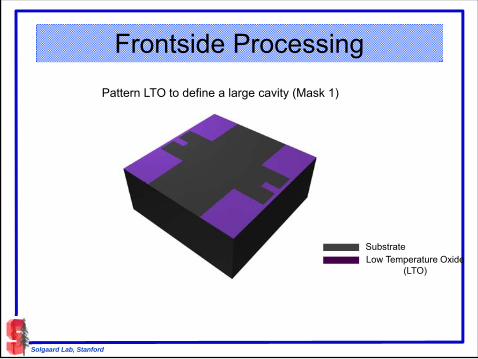
7
Solgaard Lab, Stanford
Frontside Processing
SubstrateLow Temperature Oxide
(LTO)
Deposit LTO (Low Temperature Oxide)
Solgaard Lab, Stanford
Frontside Processing
SubstrateLow Temperature Oxide
(LTO)
Pattern LTO to define a large cavity (Mask 1)
8
Solgaard Lab, Stanford
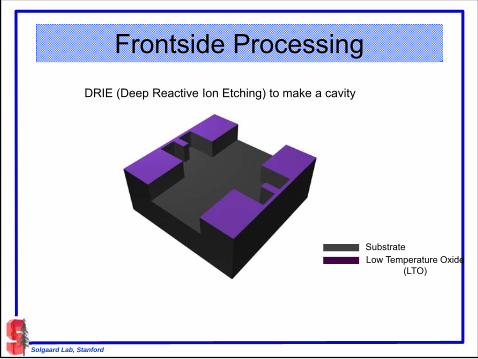
Frontside Processing
SubstrateLow Temperature Oxide
(LTO)
DRIE (Deep Reactive Ion Etching) to make a cavity
Solgaard Lab, Stanford
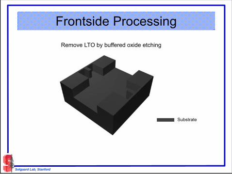
Frontside Processing
Substrate
Remove LTO by buffered oxide etching
8
Solgaard Lab, Stanford
Frontside Processing
SubstrateLow Temperature Oxide
(LTO)
DRIE (Deep Reactive Ion Etching) to make a cavity
Solgaard Lab, Stanford
Frontside Processing
Substrate
Remove LTO by buffered oxide etching
9
Solgaard Lab, Stanford
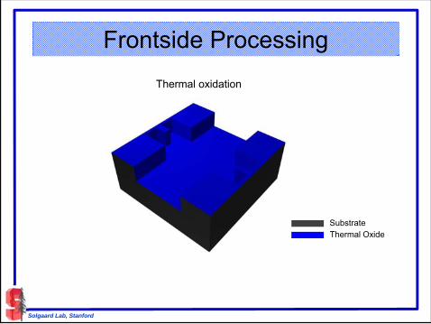
Frontside Processing
SubstrateThermal Oxide
Thermal oxidation
Solgaard Lab, Stanford
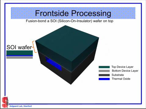
Frontside Processing
SubstrateThermal Oxide
Top Device Layer Bottom Device Layer
Fusion-bond a SOI (Silicon-On-Insulator) wafer on top
SOI wafer
9
Solgaard Lab, Stanford
Frontside Processing
SubstrateThermal Oxide
Thermal oxidation
Solgaard Lab, Stanford
Frontside Processing
SubstrateThermal Oxide
Top Device Layer Bottom Device Layer
Fusion-bond a SOI (Silicon-On-Insulator) wafer on top
SOI wafer
10
Solgaard Lab, Stanford
Frontside Processing
SubstrateThermal Oxide
Top Device Layer Bottom Device Layer
Grind and polish the substrate of the SOI wafer
Solgaard Lab, Stanford
Frontside Processing
SubstrateThermal Oxide
Top Device Layer Bottom Device Layer
Low Temperature Oxide(LTO)
Self-alignment mask patterning of LTO (Mask 2)
10
Solgaard Lab, Stanford
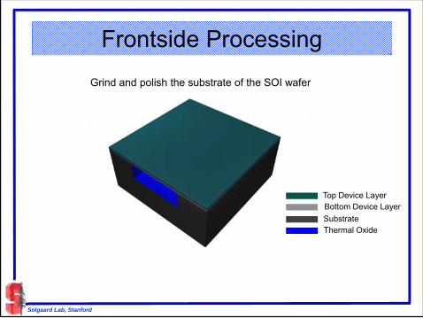
Frontside Processing
SubstrateThermal Oxide
Top Device Layer Bottom Device Layer
Grind and polish the substrate of the SOI wafer
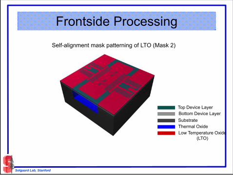
Solgaard Lab, Stanford
Frontside Processing
SubstrateThermal Oxide
Top Device Layer Bottom Device Layer
Low Temperature Oxide(LTO)
Self-alignment mask patterning of LTO (Mask 2)
11
Solgaard Lab, Stanford
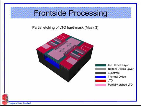
Frontside Processing
SubstrateThermal Oxide
Top Device Layer Bottom Device Layer
LTO
Partial etching of LTO hard mask (Mask 3)
Partially-etched LTO
Solgaard Lab, Stanford
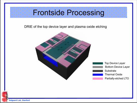
Frontside Processing
SubstrateThermal Oxide
Top Device Layer Bottom Device Layer
DRIE of the top device layer and plasma oxide etching
Partially-etched LTO
11
Solgaard Lab, Stanford
Frontside Processing
SubstrateThermal Oxide
Top Device Layer Bottom Device Layer
LTO
Partial etching of LTO hard mask (Mask 3)
Partially-etched LTO
Solgaard Lab, Stanford
Frontside Processing
SubstrateThermal Oxide
Top Device Layer Bottom Device Layer
DRIE of the top device layer and plasma oxide etching
Partially-etched LTO
12
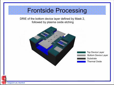
Solgaard Lab, Stanford
Frontside Processing
SubstrateThermal Oxide
Top Device Layer Bottom Device Layer
DRIE of the bottom device layer defined by Mask 2, followed by plasma oxide etching
Solgaard Lab, Stanford
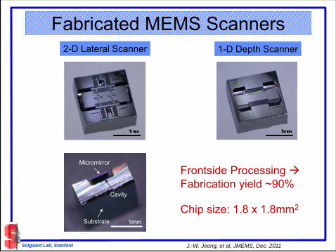
Fabricated MEMS Scanners2-D Lateral Scanner 1-D Depth Scanner
Chip size: 1.8 x 1.8mm2
1mmSubstrate
Micromirror
Cavity
J.-W. Jeong, et al, JMEMS, Dec. 2011
Frontside Processing Fabrication yield ~90%
12
Solgaard Lab, Stanford
Frontside Processing
SubstrateThermal Oxide
Top Device Layer Bottom Device Layer
DRIE of the bottom device layer defined by Mask 2, followed by plasma oxide etching
Solgaard Lab, Stanford
Fabricated MEMS Scanners2-D Lateral Scanner 1-D Depth Scanner
Chip size: 1.8 x 1.8mm2
1mmSubstrate
Micromirror
Cavity
J.-W. Jeong, et al, JMEMS, Dec. 2011
Frontside Processing Fabrication yield ~90%
13
Solgaard Lab, Stanford
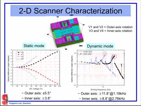
2-D Scanner Characterization
0 20 40 60 80 100 120 140 160 180 200-6
-5
-4
-3
-2
-1
0
1
2
3
4
5
6
Opt
ical
def
lect
ion
angl
e (d
egre
e)
DC voltage (V)
V2 V1 V3 V4
102
103
10-2
10-1
100
101
Opt
ical
def
lect
ion
ang
le (
degr
ee)
Driving frequency (Hz)
Outer axis Inner axis
− Outer axis: ±5.5°
− Inner axis: ±3.8°− Outer axis: ±11.8°@1.18kHz
− Inner axis: ±8.8°@2.76kHz
V1 and V2 = Outer-axis rotationV3 and V4 = Inner-axis rotation
Static mode Dynamic mode
Solgaard Lab, Stanford
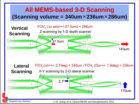
All MEMS-based 3-D Scanning(Scanning volume = 340um×236um×286um)
143um
27.5um
Z-scanning by 1-D depth scanner
2.7º
170um
X-Y scanning by 2-D lateral scanner
FOVz (z axis=+/-27.5um) = 286um
FOVx(=+/- 2.7deg) = 340um / FOVy (Dq=+/- 1.9deg) = 236um
J.-W. Jeong, et al, Optical MEMS and Nanophotonics, 2011
Vertical Scanning
Lateral Scanning
13
Solgaard Lab, Stanford
2-D Scanner Characterization
0 20 40 60 80 100 120 140 160 180 200-6
-5
-4
-3
-2
-1
0
1
2
3
4
5
6
Opt
ical
def
lect
ion
angl
e (d
egre
e)
DC voltage (V)
V2 V1 V3 V4
102
103
10-2
10-1
100
101
Opt
ical
def
lect
ion
ang
le (
degr
ee)
Driving frequency (Hz)
Outer axis Inner axis
− Outer axis: ±5.5°
− Inner axis: ±3.8°− Outer axis: ±11.8°@1.18kHz
− Inner axis: ±8.8°@2.76kHz
V1 and V2 = Outer-axis rotationV3 and V4 = Inner-axis rotation
Static mode Dynamic mode
Solgaard Lab, Stanford
All MEMS-based 3-D Scanning(Scanning volume = 340um×236um×286um)
143um
27.5um
Z-scanning by 1-D depth scanner
2.7º
170um
X-Y scanning by 2-D lateral scanner
FOVz (z axis=+/-27.5um) = 286um
FOVx(=+/- 2.7deg) = 340um / FOVy (Dq=+/- 1.9deg) = 236um
J.-W. Jeong, et al, Optical MEMS and Nanophotonics, 2011
Vertical Scanning
Lateral Scanning
14
Solgaard Lab, Stanford
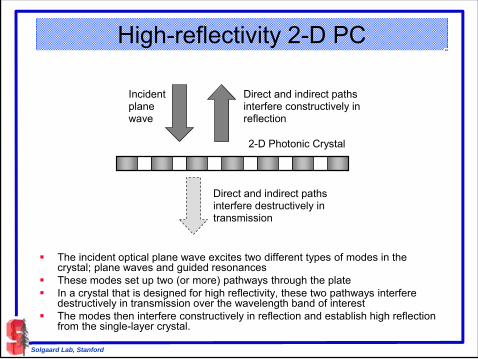
High-reflectivity 2-D PC
The incident optical plane wave excites two different types of modes in the crystal; plane waves and guided resonances
These modes set up two (or more) pathways through the plate In a crystal that is designed for high reflectivity, these two pathways interfere
destructively in transmission over the wavelength band of interest The modes then interfere constructively in reflection and establish high reflection
from the single-layer crystal.
Incident plane wave
Direct and indirect paths interfere destructively in transmission
Direct and indirect paths interfere constructively in reflection
2-D Photonic Crystal
Solgaard Lab, Stanford
0
0.1
0.2
0.3
0.4
0.5
0.6
0.7
0.8
0.9
1
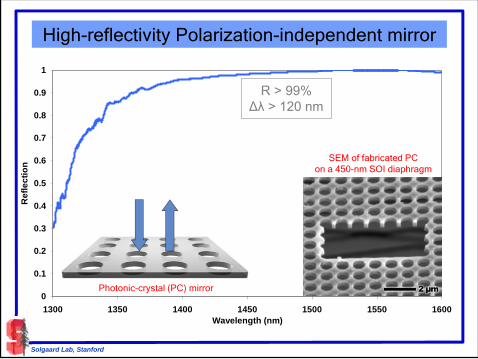
1300 1350 1400 1450 1500 1550 1600Wavelength (nm)
Re
fle
cti
on
R > 99%∆λ > 120 nm
High-reflectivity Polarization-independent mirror
Photonic-crystal (PC) mirror
SEM of fabricated PCon a 450-nm SOI diaphragm
14
Solgaard Lab, Stanford
High-reflectivity 2-D PC
The incident optical plane wave excites two different types of modes in the crystal; plane waves and guided resonances
These modes set up two (or more) pathways through the plate In a crystal that is designed for high reflectivity, these two pathways interfere
destructively in transmission over the wavelength band of interest The modes then interfere constructively in reflection and establish high reflection
from the single-layer crystal.
Incident plane wave
Direct and indirect paths interfere destructively in transmission
Direct and indirect paths interfere constructively in reflection
2-D Photonic Crystal
Solgaard Lab, Stanford
0
0.1
0.2
0.3
0.4
0.5
0.6
0.7
0.8
0.9
1
1300 1350 1400 1450 1500 1550 1600Wavelength (nm)
Re
fle
cti
on
R > 99%∆λ > 120 nm
High-reflectivity Polarization-independent mirror
Photonic-crystal (PC) mirror
SEM of fabricated PCon a 450-nm SOI diaphragm
15
Solgaard Lab, Stanford
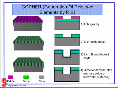
GOPHER (Generation Of PHotonicElements by RIE)
1) Lithography
2)Etch oxide mask
3)Etch Si and deposit oxide
PMMA Oxide Silicon
4) Directional oxide etch (remove oxide on horizontal surfaces)
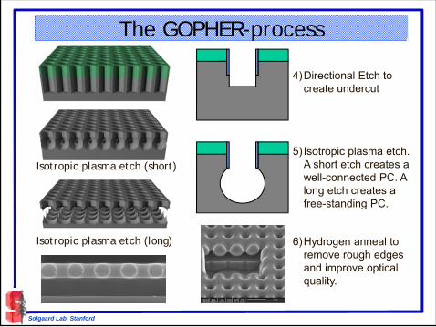
Solgaard Lab, Stanford
The GOPHER-process
Isotropic plasma etch (short)
4)Directional Etch to create undercut
Isotropic plasma etch (long)
5) Isotropic plasma etch. A short etch creates a well-connected PC. A long etch creates a free-standing PC.
6)Hydrogen anneal to remove rough edges and improve optical quality.
15
Solgaard Lab, Stanford
GOPHER (Generation Of PHotonicElements by RIE)
1) Lithography
2)Etch oxide mask
3)Etch Si and deposit oxide
PMMA Oxide Silicon
4) Directional oxide etch (remove oxide on horizontal surfaces)
Solgaard Lab, Stanford
The GOPHER-process
Isotropic plasma etch (short)
4)Directional Etch to create undercut
Isotropic plasma etch (long)
5) Isotropic plasma etch. A short etch creates a well-connected PC. A long etch creates a free-standing PC.
6)Hydrogen anneal to remove rough edges and improve optical quality.
16
Solgaard Lab, Stanford
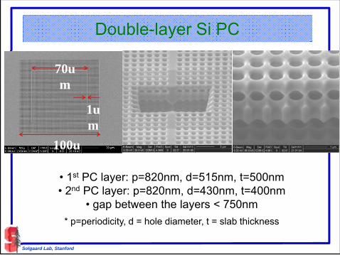
Double-layer Si PC
70um
100um
1um
• 1st PC layer: p=820nm, d=515nm, t=500nm• 2nd PC layer: p=820nm, d=430nm, t=400nm
• gap between the layers < 750nm
* p=periodicity, d = hole diameter, t = slab thickness
Solgaard Lab, Stanford
Fabry-Perots with PC mirrors
PC mirrors
High reflectivity in IR
(99.5% reflectivity)
Thermally robust
High power handling
Flexible polarization
Single dielectric layer
MEMS compatible, flexible post processing
Complex phase response
Small angular range
Limited wavelength rangeFabry-Perot
Mirror on fiber facet
Acoustic wave Photonic-crystal mirror
Single-mode fiber
16
Solgaard Lab, Stanford
Double-layer Si PC
70um
100um
1um
• 1st PC layer: p=820nm, d=515nm, t=500nm• 2nd PC layer: p=820nm, d=430nm, t=400nm
• gap between the layers < 750nm
* p=periodicity, d = hole diameter, t = slab thickness
Solgaard Lab, Stanford
Fabry-Perots with PC mirrors
PC mirrors
High reflectivity in IR
(99.5% reflectivity)
Thermally robust
High power handling
Flexible polarization
Single dielectric layer
MEMS compatible, flexible post processing
Complex phase response
Small angular range
Limited wavelength rangeFabry-Perot
Mirror on fiber facet
Acoustic wave Photonic-crystal mirror
Single-mode fiber
17
Solgaard Lab, Stanford
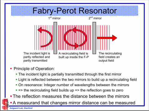
Fabry-Perot Resonator
The recirculating field creates an output field
A recirculating field is built up inside the F-P
The incident light is partly reflected and partly transmitted
1st mirror 2nd mirror
Principle of Operation: The incident light is partially transmitted through the first mirror
Light is reflected between the two mirrors to build up a recirculating field
On resonance: Integer number of wavelengths between the mirrors
=> the recirculating field builds up => the reflection goes to zero
The reflection measures the distance between the mirrors
A measurand that changes mirror distance can be measured
Solgaard Lab, Stanford
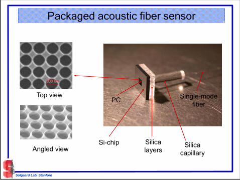
Packaged acoustic fiber sensor
Si-chip
PC
Silica layers
Silica capillary
Single-mode fiber
Top view
Angled view
17
Solgaard Lab, Stanford
Fabry-Perot Resonator
The recirculating field creates an output field
A recirculating field is built up inside the F-P
The incident light is partly reflected and partly transmitted
1st mirror 2nd mirror
Principle of Operation: The incident light is partially transmitted through the first mirror
Light is reflected between the two mirrors to build up a recirculating field
On resonance: Integer number of wavelengths between the mirrors
=> the recirculating field builds up => the reflection goes to zero
The reflection measures the distance between the mirrors
A measurand that changes mirror distance can be measured
Solgaard Lab, Stanford
Packaged acoustic fiber sensor
Si-chip
PC
Silica layers
Silica capillary
Single-mode fiber
Top view
Angled view
18
Solgaard Lab, Stanford
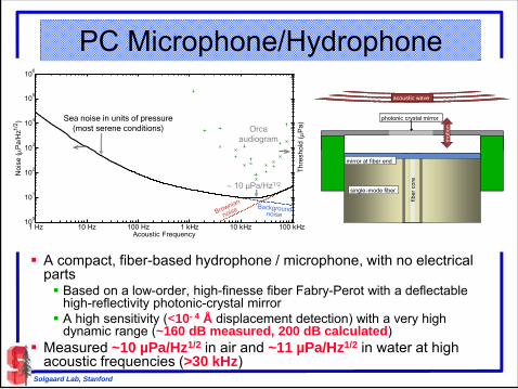
1 Hz 10 Hz 100 Hz 1 kHz 10 kHz 100 kHz10
0
101
102
103
104
105
106
Noi
se (P
a/H
z1/2 )
Acoustic Frequency
Thr
esh
old
( P
a)
10 µPa/Hz1/2
Sea noise in units of pressure(most serene conditions)
Brownian
noiseBackground
noise
Orca audiogram
PC Microphone/Hydrophone
A compact, fiber-based hydrophone / microphone, with no electrical parts Based on a low-order, high-finesse fiber Fabry-Perot with a deflectable
high-reflectivity photonic-crystal mirror A high sensitivity (<10-4 Å displacement detection) with a very high
dynamic range (~160 dB measured, 200 dB calculated) Measured ~10 µPa/Hz1/2 in air and ~11 µPa/Hz1/2 in water at high
acoustic frequencies (>30 kHz)
acoustic wave
mot
ion
fiber
cor
e
single-mode fiber
photonic crystal mirror
mirror at fiber end
acoustic wave
mot
ion
fiber
cor
e
single-mode fiber
photonic crystal mirror
mirror at fiber end
Solgaard Lab, Stanford
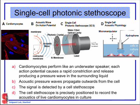
Single-cell photonic stethoscope
a) Cardiomyocytes perform like an underwater speaker; each action potential causes a rapid constriction and release producing a pressure wave in the surrounding liquid
b) Acoustic pressure waves propagate outwards from the cell
c) The signal is detected by a cell stethoscope
d) The cell stethoscope is precisely positioned to record the acoustics of live cardiomyocytes in culture
18
Solgaard Lab, Stanford
1 Hz 10 Hz 100 Hz 1 kHz 10 kHz 100 kHz10
0
101
102
103
104
105
106
Noi
se (P
a/H
z1/2 )
Acoustic Frequency
Thr
esh
old
( P
a)
10 µPa/Hz1/2
Sea noise in units of pressure(most serene conditions)
Brownian
noiseBackground
noise
Orca audiogram
PC Microphone/Hydrophone
A compact, fiber-based hydrophone / microphone, with no electrical parts Based on a low-order, high-finesse fiber Fabry-Perot with a deflectable
high-reflectivity photonic-crystal mirror A high sensitivity (<10-4 Å displacement detection) with a very high
dynamic range (~160 dB measured, 200 dB calculated) Measured ~10 µPa/Hz1/2 in air and ~11 µPa/Hz1/2 in water at high
acoustic frequencies (>30 kHz)
acoustic wave
mot
ion
fiber
cor
e
single-mode fiber
photonic crystal mirror
mirror at fiber end
acoustic wave
mot
ion
fiber
cor
e
single-mode fiber
photonic crystal mirror
mirror at fiber end
Solgaard Lab, Stanford
Single-cell photonic stethoscope
a) Cardiomyocytes perform like an underwater speaker; each action potential causes a rapid constriction and release producing a pressure wave in the surrounding liquid
b) Acoustic pressure waves propagate outwards from the cell
c) The signal is detected by a cell stethoscope
d) The cell stethoscope is precisely positioned to record the acoustics of live cardiomyocytes in culture
19
Solgaard Lab, Stanford
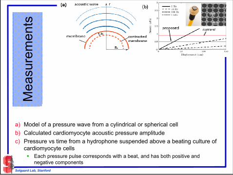
Mea
sure
men
ts
a) Model of a pressure wave from a cylindrical or spherical cell
b) Calculated cardiomyocyte acoustic pressure amplitude
c) Pressure vs time from a hydrophone suspended above a beating culture of cardiomyocyte cells Each pressure pulse corresponds with a beat, and has both positive and
negative components
Solgaard Lab, Stanford
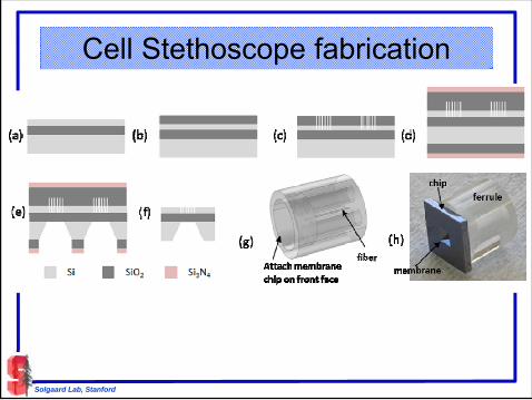
Cell Stethoscope fabrication
19
Solgaard Lab, Stanford
Mea
sure
men
ts
a) Model of a pressure wave from a cylindrical or spherical cell
b) Calculated cardiomyocyte acoustic pressure amplitude
c) Pressure vs time from a hydrophone suspended above a beating culture of cardiomyocyte cells Each pressure pulse corresponds with a beat, and has both positive and
negative components
Solgaard Lab, Stanford
Cell Stethoscope fabrication
20
Solgaard Lab, Stanford
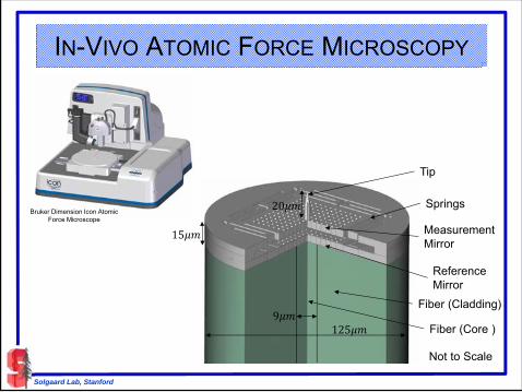
IN-VIVO ATOMIC FORCE MICROSCOPY
Tip
Springs
Measurement Mirror
Reference Mirror
Fiber (Cladding)
Not to Scale
Fiber (Core )9
125
20
15
Bruker Dimension Icon Atomic Force Microscope
Solgaard Lab, Stanford
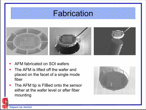
Fabrication
AFM fabricated on SOI wafers
The AFM is lifted off the wafer and placed on the facet of a single mode fiber
The AFM tip is FIBed onto the sensor either at the wafer level or after fiber mounting
20
Solgaard Lab, Stanford
IN-VIVO ATOMIC FORCE MICROSCOPY
Tip
Springs
Measurement Mirror
Reference Mirror
Fiber (Cladding)
Not to Scale
Fiber (Core )9
125
20
15
Bruker Dimension Icon Atomic Force Microscope
Solgaard Lab, Stanford
Fabrication
AFM fabricated on SOI wafers
The AFM is lifted off the wafer and placed on the facet of a single mode fiber
The AFM tip is FIBed onto the sensor either at the wafer level or after fiber mounting
21
Solgaard Lab, Stanford
Distance From Sample
Attractive Force
Adhesive Force
Repulsive Force
Time (ms)
Reflectance
Photodiode
Laser
Device
3dB Coupler
PhotodiodeReflected Power
Transmitted Power
Relative D
isplacement
Measurement Setup
Oscillating Sample
Fixed Reference Mirror
Moving Measurement Mirror
Solgaard Lab, Stanford
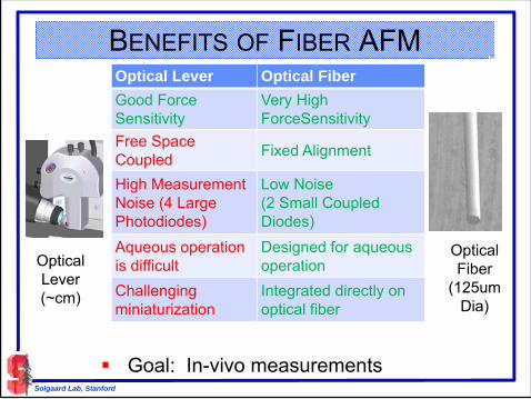
BENEFITS OF FIBER AFMOptical Lever Optical Fiber
Good Force Sensitivity
Very High ForceSensitivity
Free Space Coupled
Fixed Alignment
High Measurement Noise (4 Large Photodiodes)
Low Noise(2 Small Coupled Diodes)
Aqueous operationis difficult
Designed for aqueous operation
Challenging miniaturization
Integrated directly on optical fiber
Goal: In-vivo measurements
Optical Lever(~cm)
Optical Fiber
(125um Dia)
21
Solgaard Lab, Stanford
Distance From Sample
Attractive Force
Adhesive Force
Repulsive Force
Time (ms)
Reflectance
Photodiode
Laser
Device
3dB Coupler
PhotodiodeReflected Power
Transmitted Power
Relative D
isplacement
Measurement Setup
Oscillating Sample
Fixed Reference Mirror
Moving Measurement Mirror
Solgaard Lab, Stanford
BENEFITS OF FIBER AFMOptical Lever Optical Fiber
Good Force Sensitivity
Very High ForceSensitivity
Free Space Coupled
Fixed Alignment
High Measurement Noise (4 Large Photodiodes)
Low Noise(2 Small Coupled Diodes)
Aqueous operationis difficult
Designed for aqueous operation
Challenging miniaturization
Integrated directly on optical fiber
Goal: In-vivo measurements
Optical Lever(~cm)
Optical Fiber
(125um Dia)
22
Solgaard Lab, Stanford
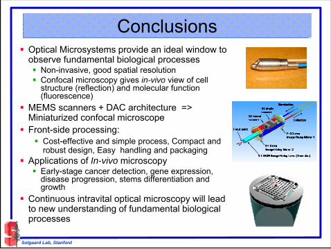
Conclusions Optical Microsystems provide an ideal window to
observe fundamental biological processes Non-invasive, good spatial resolution Confocal microscopy gives in-vivo view of cell
structure (reflection) and molecular function (fluorescence)
MEMS scanners + DAC architecture =>Miniaturized confocal microscope
Front-side processing: Cost-effective and simple process, Compact and
robust design, Easy handling and packaging Applications of In-vivo microscopy Early-stage cancer detection, gene expression,
disease progression, stems differentiation and growth
Continuous intravital optical microscopy will lead to new understanding of fundamental biological processes