ieee journal of solid-state circuits, vol. …rnavid/index_files/papers/16gbpsjssc.pdf... member,...
TRANSCRIPT

IEEE JOURNAL OF SOLID-STATE CIRCUITS, VOL. 44, NO. 4, APRIL 2009 1235
A 16 Gb/s/Link, 64 GB/s Bidirectional AsymmetricMemory Interface
Haechang Lee, Member, IEEE, Kun-Yung Ken Chang, Member, IEEE, Jung-Hoon Chun, Member, IEEE,Ting Wu, Member, IEEE, Yohan Frans, Member, IEEE, Brian Leibowitz, Member, IEEE, Nhat Nguyen, T. J. Chin,
Kambiz Kaviani, Member, IEEE, Jie Shen, Xudong Shi, Wendemagegnehu T. Beyene, Senior Member, IEEE,Simon Li, Reza Navid, Member, IEEE, Marko Aleksic, Member, IEEE, Fred S. Lee, Member, IEEE, Fredy Quan,
Jared Zerbe, Member, IEEE, Rich Perego, and Fariborz Assaderaghi, Senior Member, IEEE
Abstract—This paper describes a bidirectional, differential,16 Gb/s per link memory interface that includes a Controllerand an emulated DRAM physical interface (PHY) designed in65 nm CMOS. To achieve high data rate, the interface employsthe following technology ingredients: asymmetric equalization,asymmetric timing calibration, asymmetric link margining, in-ductor based (LC) PLLs, multi-phase error correction, and a datadependent regulator. At 16 Gb/s, this interface achieves a unit-in-terval to inverter FO4 ratio of 2.8 (Controller) and 1.4 (DRAM)and operates in a channel with 15 dB loss at Nyquist. Under suchbandwidth limitations on and off chip, the Controller and DRAMPHYs consume 13 mW/Gb/s and 8 mW/Gb/s, respectively. UsingPRBS 2�� 1, the link achieves a timing margin of 0.19 UI at aBER of 1e-12 for both read and write operations.
Index Terms—CMOS memory integrated circuits, DRAM chips,equalizers, high-speed integrated circuits, interconnections, inter-symbol interference, jitter, synchronization, transceivers.
I. INTRODUCTION
S YSTEM memory bandwidth is one of the key limitationsto high performance computing. Total memory bandwidth
can be increased either by increasing the number of links or byincreasing the per link data rate. However, there is a cost ad-vantage to increasing the per link data rate to achieve this goalas it reduces the package size as well as the number of DRAMsand eases routing congestion that would otherwise require moremetal layers in the package and PCB. Thus, the primary objec-tive of this work is to build the fastest memory transceiver pos-sible while constraining power efficiency (mW/Gb/s) such thatthermal issues do not negate the cost savings achieved by re-ducing the number of links.
It is estimated that the total memory bandwidth required bygraphics processors and game consoles will approach 1 TB/s in
Manuscript received August 25, 2008; revised October 22, 2008. Current ver-sion published March 25, 2009.
H. Lee, K.-Y. K. Chang, T. Wu, Y. Frans, B. Leibowitz, N. Nguyen, T. J.Chin, K. Kaviani, J. Shen, X. Shi, W. T. Beyene, S. Li, M. Aleksic, F. Quan, J.Zerbe, and R. Perego are with Rambus Inc., Los Altos, CA 94022 USA (e-mail:[email protected]).
J.-H. Chun was with Rambus Inc., Los Altos, CA 94022 USA, and is nowwith the Department of Semiconductor Systems Engineering, SungKyunKwanUniversity, Suwon, Korea.
R. Navid was with Rambus Inc., Los Altos, CA 94022 USA, and is now withTrue Circuits Inc., Los Altos, CA 94022 USA.
F. Assaderaghi and F. S. Lee were with Rambus Inc., Los Altos, CA 94022USA, and are now with SiTime Corporation, Sunnyvale, CA 94085 USA.
Digital Object Identifier 10.1109/JSSC.2009.2014199
2012 [1]. The interface in this work operates at 16 Gb/s/linkin order to achieve this aggregate bandwidth with 512 links,a count that has already been demonstrated in state-of-the-artGPUs.
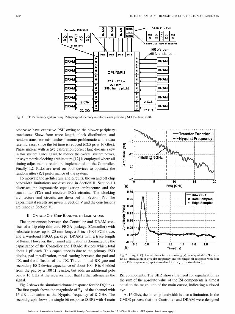
Fig. 1 illustrates such a 1 TB/s memory system [2]. It shows16 DRAMs, each of which has 32 data links (DQ) and twoCommand/Address (C/A) links all operating at 16 Gb/s. The 32DQs provide a combined data bandwidth of 64 GB/s to eachDRAM.1 Both C/A and DQ are point-to-point differential links.Point-to-point signaling provides good signal integrity by min-imizing impedance discontinuities while differential signalingis robust against common-mode noise sources such as supplynoise and ground bounce. Furthermore, differential signaling re-sults in less crosstalk/EMI and simultaneous switching outputnoise than single-ended signaling. One difference between theC/A and DQ links is that the C/A is unidirectional whereas theDQ is bidirectional.
The key technical challenges to designing 16 Gb/s memorylinks discussed in [3] and [4] are: bandwidth limitation in thechannel, bandwidth limitation on the silicon, jitter, skew, andpower efficiency. To overcome the bandwidth limitation of thechannel, an asymmetric equalization architecture that placesall the equalization capability on the Controller is used. Sincethe transistors in the Controller are about twice as fast as theperiphery devices in the DRAM in any given process genera-tion, the power of the overall system can be reduced by placingequalization circuits for both read and write directions on theController. As a reference, the inverter fanout-of-4 (FO4) gatedelay is 22 ps for the controller and 45 ps for the emulatedDRAM in this work. To further alleviate the speed limitation ofthe silicon, half rate and quadrature clocking are employed onthe Controller and DRAM, respectively, to reduce the on-chipclock rates. Since high frequency jitter is amplified whenpassing through a low pass channel [5], duty cycle correctionand quadrature correction are employed in the Controller andDRAM respectively to reduce deterministic jitter (DJ). Thespeed limitation of the silicon exacerbates another type of jitter,namely power-supply induced jitter (PSIJ) which cannot be al-leviated with multi-phase clocking. A data-dependent regulatorpowers the datapath and clock tree of the DRAM which would
1The two C/A links to each DRAM enables a 64-byte access granularity. A32-byte granularity can be achieved simply by adding two more C/A links perDRAM. The 2� improvement in granularity would increase the area and powerof the interface by only 6%.
0018-9200/$25.00 © 2009 IEEE
Authorized licensed use limited to: Stanford University. Downloaded on September 27, 2009 at 18:45 from IEEE Xplore. Restrictions apply.
1236 IEEE JOURNAL OF SOLID-STATE CIRCUITS, VOL. 44, NO. 4, APRIL 2009
Fig. 1. 1 TB/s memory system using 16 high speed memory interfaces each providing 64 GB/s bandwidth.
otherwise have excessive PSIJ owing to the slower peripherytransistors. Skew from trace length, clock distribution, andrandom transistor mismatches become problematic as the datarate increases since the bit time is reduced (62.5 ps at 16 Gb/s).Phase mixers with active calibration correct lane-to-lane skewin this system. Once again, to reduce the overall system power,an asymmetric clocking architecture [12] is employed where alltiming adjustment circuits are implemented on the Controller.Finally, LC PLLs are used on both devices to optimize therandom jitter (RJ) performance of the system.
To motivate the architecture and circuits, the on and off chipbandwidth limitations are discussed in Section II. Section IIIdiscusses the asymmetric equalization architecture and thetransmitter (TX) and receiver (RX) circuits. The clockingarchitecture and circuits are described in Section IV. Theexperimental results are given in Section V and the conclusionsare made in Section VI.
II. ON AND OFF CHIP BANDWIDTH LIMITATIONS
The interconnect between the Controller and DRAM con-sists of a flip-chip thin-core FBGA package (Controller) withsubstrate traces up to 20-mm long, a 3-inch FR4 PCB trace,and a wirebond FBGA package (DRAM) with a trace lengthof 8-mm. However, the channel attenuation is dominated by thecapacitance of the Controller and DRAM devices which totalabout 1 pF each. This capacitance is due to the primary ESDdiodes, pad metallization, metal routing between the pad andTX, and the diffusion of the TX. The combined RX gate andsecondary ESD device capacitance of about 100 fF is shieldedfrom the pad by a 100 resistor, but adds an additional polebelow 16 GHz at the receiver input that further attenuates thesignal.
Fig. 2 shows the simulated channel response for the DQ links.The first graph shows the magnitude of of the channel with15 dB attenuation at the Nyquist frequency of 8 GHz. Thesecond graph shows the single bit response (SBR) with 4 main
Fig. 2. Target DQ channel characteristic showing (a) the magnitude of � with15 dB attenuation at Nyquist frequency and (b) single bit response with fourmain ISI components (input normalized to 1 � in simulation).
ISI components. The SBR shows the need for equalization asthe sum of the absolute value of the ISI components is almostequal to the magnitude of the main cursor, indicating a closedeye.
At 16 Gb/s, the on-chip bandwidth is also a limitation. In theCMOS process that the Controller and DRAM were designed
Authorized licensed use limited to: Stanford University. Downloaded on September 27, 2009 at 18:45 from IEEE Xplore. Restrictions apply.

LEE et al.: A 16 Gb/s/Link, 64 GB/s BIDIRECTIONAL ASYMMETRIC MEMORY INTERFACE 1237
Fig. 3. Asymmetric link architecture places equalization, clocking, and link diagnostic complexity on the Controller for improved power efficiency.
in, the FO4 inverter delays are 22 ps and 45 ps, respectively,in the slow device, low voltage, high temperature corner. Thistranslates into a low unit-interval to inverter FO4 ratio (UI/FO4)of 2.8 (Controller) and 1.4 (DRAM). Prior research showed thatthe minimum clock period to pass through a FO4 chain of in-verters without amplitude reduction is 8-FO4 [6]. This meansthat the high speed portions of this design will require logic witheffective FO less than 4. In fact, the required FO of the clocktrees approaches 2 for double data rate at the Controller andquad data rate at the DRAM. The primary cost of low FO designis added power consumption. A related observation is that de-signing a given circuit in the Controller is more power efficientthan designing it in the DRAM. This is true for analog circuits aswell as logic, as the lower and high thresholds in the DRAMprocess degrade amplifier power efficiency. This is the motiva-tion behind the asymmetric memory link architecture, shown inFig. 3, where the Controller contains more of the timing, equal-ization, and link diagnostic circuitry. The details will be coveredin subsequent sections.
In addition to the slower devices, DRAM processes also havefewer metal layers (at most 3) which have higher resistivity andlarger capacitance to the substrate than those for ASICs. Thislimits the options for on-chip inductors as well as global clockand power grid distribution.
On a final note, we want to make clear that the DRAM pre-sented in this paper is an emulated DRAM. Since this memorylink is designed for production in the 2010–2012 timeframe,the process does not exist yet. Hence, to validate the architec-ture and ideas set forth, a 65 nm CMOS process was degraded(by design constraints) to match the best estimates on the futureDRAM process. For example, non minimum length and highthreshold devices were exclusively used to match the thresholdvoltage and the FO4 of the future DRAM process and metalusage was restricted to three routing layers as described in [4].In contrast, the ASIC process in the 2010–2012 timeframe willbe faster than the 65 nm CMOS process used for the Controller.Hence, the power efficiency (mW/Gb/s) of the Controller willimprove in the future process.
III. EQUALIZATION ARCHITECTURE AND CIRCUITS
As shown in Fig. 3, the Controller provides equalizationfor both write and read operations. In the write direction,the channel is equalized using a 5-tap TX FIR.2 In the readdirection, an analog linear equalizer provides about 6 dB ofemphasis at the Nyquist frequency of 8 GHz. As the write andread directions leverage different equalizers, some performancemismatch between them is expected, but they are designedto offer similar performance to prevent one direction fromlimiting the overall system margin. Based on signal integritysimulations, the nominal swing of the Controller (DC swingwithout equalization) is made 50% larger than the DRAM forthis purpose. The DRAM TX output swing is set to 540 mV
11 mA so that its high threshold transistors havesufficient saturation margin. The Controller swing is thus800 mV 16 mA .
A. Transmit FIR and Link Diagnostic Circuits
A block diagram of the Controller TX is shown in Fig. 4. Ithas 5 FIR taps (1 pre, 1 main, 3 post) to equalize the SBR ofFig. 2. Each segment has a 2:1 multiplexing pre-driver that seri-alizes the 8 Gb/s input into a full rate 16 Gb/s stream. The outputdrivers are open-drain differential pairs with digitally controlledtail current sources for tap weight adjustment.
The FIR circuits necessary for equalization are also used toevaluate the performance of the link. With minor reconfigurationenabled by digital registers, the Controller TX can add a DC dif-ferential voltage offset into the channel so that the voltage margincan be measured. This is important because while the write eyeat the pad of the DRAM is relatively wide open due to the Con-troller TX-FIR, the read eye at the pad of the Controller will beseverely degraded since the effect of equalization is only visibleon chip at the output of the Controller RX. This is illustrated bythe eye diagrams in Fig. 3.3 Hence, it is not possible to verify the
2The DRAM RX amplifier has 3 dB nominal gain and can be configured toprovide some equalization of on-chip losses via de-emphasis, but is not capableof equalizing the ISI shown in Fig. 2.
3The eye diagrams in Fig. 3 are for illustration only and are not the actualeyes at the pads.
Authorized licensed use limited to: Stanford University. Downloaded on September 27, 2009 at 18:45 from IEEE Xplore. Restrictions apply.

1238 IEEE JOURNAL OF SOLID-STATE CIRCUITS, VOL. 44, NO. 4, APRIL 2009
Fig. 4. (a) Block diagram, and conceptual schematics of (b) normal write mode, (c) margining write mode, and (d) margining read mode of segmentedController TX.
functionality of the equalizers by observing eye diagrams on anexternal scope. The ability to add a voltage offset combined withtiming control from the phase mixers enables the Controller tomap the effective BER eye diagram in voltage and time for theentire link, including the RX circuits themselves. There are twodistinct features in our implementation compared to [7] and [8]:the first is that the voltage offset is added by the transmitter ratherthan the receiver and the second is that the Controller transmitteradds the voltage offset to margin the link for both the write andread operations. These features leverage both the asymmetry andthe bidirectionality of the link. Fig. 4(b)–(d) shows how the Con-troller TX is reconfigured for the various modes of operation.Conceptually, each TX tap driver consists of 3 separate segments.The first segment consumes half the current and the sum of theother 2 segments makes up the other half. During normal writeoperation, all three segments are driven with data by their respec-tive pre-drivers. When the write direction is margined, only thefirst segment (‘Data Segment’) is connected to its pre-driver andtransmits data. The second segment (‘Offset Segment’) is hardswitched to add a differential offset to the channel. The polarityof the offset is set by which transistor of the differential pair isconnected to supply and which is connected to ground. The mag-nitude of the offset is adjusted with the digital code to thetail current source. The inputs of the third differential pair (‘CMSegment’) are both tied to the supply to pull both output nodesdown. The current of the CM segment is set according toconstraints (1) and (2) so that the output common-mode level iskept constant even as the offset is varied. Essentially, the Con-troller TX is adding a differential offset to its own signal on thechannel. When margining the read direction, the DRAM TX isput in half swing mode and the Data Segment of the Controller
TX is now turned off. The Offset and CM segments are still en-abled. As mentioned before, the swing of the DRAM is less thanthe Controller, so the current of the Offset and CM Segments arescaled by the same proportion to maintain the common mode ofthe signal at the input of the Controller RX. In this manner, theController TX adds a differential offset to the signal from theDRAM.
(1)
(2)
B. Controller Receive Equalizer
The Controller RX shown in Fig. 5(a) starts with a contin-uous time equalizer (i.e. linear equalizer). The RX then splitsinto two sampling paths (even and odd) to relieve the maximumon-chip clock frequency. The circuits are kept as small as pos-sible to minimize power consumption, and the resulting randommismatch components are corrected via current summing at thesampler inputs. The simulated mismatch of the complete RXhas a standard deviation of 12 mV referred to the input of thesamplers where the correction takes place. The offset correctionrange is 40 mV with 3 mV resolution.
A linear equalizer is chosen over the more versatile decisionfeedback equalizer (DFE) to avoid having a feedback path of3 FO4. Unlike the more prevalent source degenerated and re-sistor loaded topology [9], the linear equalizer in Fig. 5(b) usesactive inductor loads [10] to provide emphasis in its transferfunction. Hence, the DC gain is not changed when varying thepeaking in the transfer function, as seen in Fig. 5(c). The activeinductor topology was chosen as simulations showed that it pro-vides 3 dB more emphasis than the source degenerated topology
Authorized licensed use limited to: Stanford University. Downloaded on September 27, 2009 at 18:45 from IEEE Xplore. Restrictions apply.

LEE et al.: A 16 Gb/s/Link, 64 GB/s BIDIRECTIONAL ASYMMETRIC MEMORY INTERFACE 1239
Fig. 5. (a) Controller RX block diagram, (b) linear equalizer using active inductor loads, and (c) AC response in nominal corner.
when the input gate size, current consumption, and DC gain arekept equal.
The active inductor equalizer is not without its challenges.For Vdd referenced signaling, the active inductor loads need tobe biased with a gate voltage higher than Vdd (Vbh) in orderto provide significant output swing. A good choice for Vbh is
such that the load device remains saturated and stillacts as an inductor for all output voltages. Vbh is generated by avoltage boosting circuit similar to [11] with an added feedbackloop to compensate for various losses from PVT and input clockconditions.
The transfer function of the equalizer can be expressed as(3). is the load capacitance, is the transconductance ofthe input device, and is the transconductance of the load.To simplify the analysis, the finite output impedance of the de-vices as well as any parasitic capacitance between the gate ofthe active inductor and (AC) ground were ignored. However,care must be taken to minimize this parasitic capacitance as itreduces the effective inductance. The frequency of the zero canbe lowered, and the peak gain increased, by either increasingor . Digitally controlled resistors are used for to provideadjustable peaking of the AC response. NMOS accumulationmode capacitors were added to supplement the inherent Cgs ofthe load device to increase the peaking.
(3)
Fig. 5(c) shows a family of transfer function curves simulatedin the nominal corner for the complete receiver. The DC gainis 2.5 dB at all settings, and the AC gain is controllable from6–9 dB to provide up to 6.5 dB of emphasis.
IV. CLOCKING ARCHITECTURE AND CIRCUITS
To ensure sufficient timing margin at 16 Gb/s, high perfor-mance clocking circuits are necessary on both the Controllerand DRAM. Therefore, LC-VCO based PLLs, which offer su-perior noise performance compared to ring-VCO based PLLs,are employed on both PHYs. Fewer and more resistive metallayers present challenges to designing an LC-VCO in a DRAMprocess. Solutions to these challenges are discussed in [4]. Alow-cost 500 MHz reference clock from an external clock partis distributed in a controlled impedance fashion to the Controllerand then to the DRAM. An asymmetric clocking architecture isemployed (Fig. 3). The burden of phase adjustment, skip, andlevelization are all placed on the Controller. The phase mixeradjusts the TX and RX clock for optimal BER performance andalso compensates the skew between bit slices to ease routing onthe board. The skip block handles the arbitrary phase clock do-main crossing between sclk and dclk (phase mixer output). Thepurpose of levelization is to address skew greater than 1 UI byequalizing the latency of the bit slices. Together, the levelizationand phase mixer enable an effective phase adjustment range of64 UI for both the TX and RX. These features are also used tocompensate C/A and DQ flight time differences as well as ref-erence clock skew across the multiple DRAMs.
Authorized licensed use limited to: Stanford University. Downloaded on September 27, 2009 at 18:45 from IEEE Xplore. Restrictions apply.

1240 IEEE JOURNAL OF SOLID-STATE CIRCUITS, VOL. 44, NO. 4, APRIL 2009
Fig. 6. Controller clocking architecture using a cascade of LC and ring-based PLLs. Each ring-based PLL is shared between two bitslices. Each bitslice has onephase mixer to correct skew in both the write and read directions.
A. Controller Clocking Architecture and Circuits
The Controller clocking architecture is shown in Fig. 6.On the top of each byte, an LC-VCO based PLL generates an8 GHz differential clock signal from the 500 MHz reference.This 8 GHz clock is divided down to 2 GHz before distributionto reduce the power consumption. Although this LC PLL re-sults in a clean clock output, there are two challenges. First, thephase mixer that adjusts dclk requires quadrature 8 GHz phasesto be interpolated. Second, a wide frequency range is desired totest the interface at different data rates. To address these, eachbyte level LC PLL is followed by local M/N ring-VCO basedPLLs which generate multiple phases over a wide frequencyrange.
To reduce power consumption, each ring PLL is shared bytwo neighboring bit slices (DQx2). The DQx2 clocking circuitsgenerate a dclk0 for bit0, a dclk1 for bit1, and a common sclk.To avoid the area and power consumption of two phase mixersper bit slice (a total of five for a DQx2 block), one phase mixer istime-multiplexed between the TX and RX of the same bit slice,since the two operate at different times in the same bidirectionalI/O. Two phase codes are obtained from separate read and writeoperation timing calibrations and provided to the shared phasemixer through a multiplexer which is appropriately selected ac-cording to the data transaction taking place.
B. DRAM Clocking Architecture and Circuits
The clocking architecture of the DRAM is shown in Fig. 7.One LC-PLL is used in each DQ byte to multiply the 500 MHzreference clock to 8 GHz. Because of the aforementionedtransistor and global metal routing limitations, the 8 GHz PLLoutput is divided and distributed as quadrature 4 GHz clocks(two pairs of differential 4 GHz clocks I/Ib and Q/Qb) to theindividual bit slices. These 4 GHz clocks are distributed inCML to minimize PSIJ. In each bit slice, these quadrature 4GHz clocks are locally converted to CMOS levels to drive thefront-end circuits of the TX and RX.
16 Gb/s operation in the DRAM is challenging even withquadrature rate operation. Of primary concern is PSIJ which isproportional to the delay of the circuit, and is not improved by
Fig. 7. DRAM PHY architecture showing clocking and supply regulation do-main.
multiphase clocking. Since the relatively slow process leads toa large circuit delay, PSIJ is more severe on the DRAM. It is notjust the clock tree that is of concern, but also the clocked TXand RX circuits that are closest to the pad. Variations in the clk-qdelay of the pulser as well as the aperture time of the RX samplerequally hurt the performance of the link. These blocks are imple-mented in CMOS due to headroom limitations and better powerefficiency than their CML counterparts. However, this comes atthe cost of higher PSIJ, which is addressed by supply regula-tion of the front-end datapath circuits and local (bit slice level)clocking circuits, as shown in Fig. 7. This approach maintains anet power advantage over a full CML datapath implementation,even with the regulator overhead.
The primary challenge of the voltage regulator design ismaintaining a stable output voltage despite the data-dependenttransient load currents of the CMOS datapath circuits. A voltageregulator with a replica load has been shown to provide powerand area efficient suppression of high frequency transient noisefrom the external supply [13]. We extend the idea by using adata-dependent replica (Fig. 8) that has a transient load current
Authorized licensed use limited to: Stanford University. Downloaded on September 27, 2009 at 18:45 from IEEE Xplore. Restrictions apply.

LEE et al.: A 16 Gb/s/Link, 64 GB/s BIDIRECTIONAL ASYMMETRIC MEMORY INTERFACE 1241
Fig. 8. Data dependent regulator reduces power supply induced jitter on DRAM.
Fig. 9. (a) Duty cycle correction (DCC) circuits for the Controller and (b)quadrature error correction (QEC) circuits for the DRAM.
proportional to that of the front-end, providing fast feed-for-ward regulation of transient load currents. When a transient loadstep occurs, the small capacitance of the replica circuit allowsthe change in VREP to be detected very quickly. The amplifiercan then quickly adjust the PMOS gate voltage to match thenew load condition before any significant change occurs in theoutput voltage VREG. The regulated load includes local clockbuffers, receive samplers, transmit pulser, and several flip-flops.The replica load is implemented with simple CMOS inverterswhich receive the same clock and data signals as the actualload, but are scaled to consume one quarter of the load current.The regulator is designed to power a 36 mA maximum loadcurrent with 300 MHz closed loop bandwidth, and an output
Fig. 10. Photomicrographs of (a) �32 Controller PHY and (b) �16 DRAMPHY.
capacitance of 100 pF. This regulator reduces the capacitancerequired to achieve a given transient load ripple by 4 . Thesimulated worst case PSRR over all frequencies is 16 dB.
C. Duty-Cycle and Quadrature Correction
High frequency jitter can be severely amplified by lossychannels [5]. Hence, both duty cycle error on the Controllerand quadrature phase error on the DRAM must be minimized.These are achieved by using a duty cycle corrector (DCC) anda quadrature error corrector (QEC), respectively, as shown inFig. 9(a) and (b).
Similar to the phase mixer on the Controller, a single digitallycontrolled DCC is time-multiplexed between the TX and the RXclocks. The clock duty cycle is adjusted toward its desired 50%value by using a duty cycle correction loop. This feedback loopdepicted in Fig. 9(a) consists of the DCC to adjust clock dutycycle, a MUX to select the clock signal to be calibrated, an in-tegrator followed by a comparator to detect the duty cycle errorpolarity, and an FSM that accordingly increments or decrements
Authorized licensed use limited to: Stanford University. Downloaded on September 27, 2009 at 18:45 from IEEE Xplore. Restrictions apply.

1242 IEEE JOURNAL OF SOLID-STATE CIRCUITS, VOL. 44, NO. 4, APRIL 2009
Fig. 11. Jitter characterization of (a) Controller LC PLL at 8 GHz, (b) Controller TX output at 16 Gb/s, and (c) DRAM TX output at 16 Gb/s.
the control code of the DCC. The duty cycle adjustment rangeis approximately 0.08 UI with an LSB of 2.5 mUI.
On the DRAM PHY, the accumulated quadrature phase errorsfrom mismatches in the global distribution, CML-to-CMOSconversion, and local clock buffers are corrected by the feed-back loop shown in Fig. 9(b). Quadrature error is detected nearthe front-end circuits by a symmetric CML XOR transcon-ductor followed by an integrator. The integrator output is thensensed by a comparator whose output is accumulated by anFSM to adjust switched capacitor loads. The resolution is20 mUI (1.25 ps at 16 Gb/s) and the range is 0.07 UI (4.5 ps).Using this scheme, quadrature error is limited by local devicemismatches in the quadrature detector itself.
V. MEASUREMENTS
The testchip was fabricated in TSMC 65 nm G+ technology.Fig. 10 shows the cell photomicrographs of a Controller inter-face with 4 C/A4 and 32 DQ links as well as a DRAM inter-face with 1 C/A and 16 DQ links. Each Controller byte has oneLC PLL, eight bit slices, and a dedicated place and route (PnR)logic block that includes pattern generators and checkers, timingmargin measurement logic, termination calibration, phase mixercontrol, etc. On the DRAM interface, the PLL on the left pro-vides high speed clocks to 8 neighboring DQ slices, while thePLL on the right provides clocks to the other 8 DQ slices as wellas to the receiver in the C/A cell for command requests. TheDRAM C/A cell also includes associated logic for commandprocessing. Memory reads and writes are targeted to 512 kbitsof on-chip SRAM to allow interface testing with various readand write activity patterns. Note that the C/A slice is placed tothe side to emulate the signal routing and timing requirementsfor a 32-bit interface with C/A in the center, which would beapproximately 8 mm wide.
The measured jitter performance of the Controller LC PLL,Controller TX output, and DRAM TX output are shown inFig. 11. The measured random jitter (RJ) of the ControllerLC-PLL output routed directly to pads is 318 fs rms and totaljitter (TJ) is 7.7 ps at a BER of 1e-12. When transmitting a2 1 PRBS pattern at 16 Gb/s, the Controller TX waveformhas RJ of 810 fs and TJ of 24.36 ps. Apart from the RJ contri-bution, the TJ increases because of power supply induced jitter(PSIJ) in the PLL/clock tree and transmitter, crosstalk from
4The extra C/A were routed off the board via SMP connectors to providevisibility of various analog/mixed signal components (e.g. TX-FIR, PLL).
Fig. 12. DRAM TX eye (a) before and (b) after quadrature correction. Eye isimproved from 34 mV � 25 ps to 68 mV � 35 ps.
adjacent bit slices, residual ISI, and reference feed-through.The DRAM TX output has a measured RJ of 378 fs and a TJ of8.2 ps when transmitting a clock pattern. The DRAM TX hasless jitter than the Controller TX since the LC drives the TXdirectly rather than passing through another ring-based PLL.The ring-based PLL provides flexibility to the Controller butincreases the RJ and PSIJ.
The effect of jitter amplification and the need for duty cycleand quadrature (IQ) correction is shown in Fig. 12. The timingmargin of the PRBS 2 DRAM TX eye increases by 10 ps withonly a 3.75 ps clock correction. Thus, the loss in this channel, asevidenced by the significant amount of ISI, more than doublesthe impact of the quadrature error on the eye size.
Fig. 13 shows measured BER bathtub curves for both writeand read directions at 16 Gb/s with a PRBS 2 1 data pattern.The measurement was taken with optimized TX/RX equaliza-tion coefficients and calibrated settings for RX voltage offset(both devices), for DCC (Controller), and for IQ correction(DRAM). Positive eye openings of 0.19 UI are observed at aBER of 1e-12 in both directions.
Fig. 14 shows the 16 Gb/s on-chip eyes measured using theasymmetric link diagnostic feature for both the write and readdirections. This in situ measurement shows the effective eye ofthe system including the complete effects of the channel, equal-ization, jitter, and all TX and RX circuit limitations. Althoughthe transmit swings are cut in half for these tests as mentionedearlier, both directions show timing margin greater than 0.3 UIand voltage margin of 25 mV at a BER of 1e-9.
To test the robustness of the memory interface, the timingmargin is measured across a byte. As shown in Fig. 15, both
Authorized licensed use limited to: Stanford University. Downloaded on September 27, 2009 at 18:45 from IEEE Xplore. Restrictions apply.

LEE et al.: A 16 Gb/s/Link, 64 GB/s BIDIRECTIONAL ASYMMETRIC MEMORY INTERFACE 1243
TABLE I.PERFORMANCE SUMMARY OF CONTROLLER (CTRL) AND DRAM
Fig. 13. 16 Gb/s BER bathtub curves of both write and read operations usingcontinuous � � � PRBS data
Fig. 14. On-chip eyes measured using the Controller TX to margin both thewrite and read directions at 16 Gb/s.
the write and read operations have timing margin greater than0.5 UI at a BER of 1e-3. The effect of bus turnaround (the act ofpowering on and off the TX or RX between transactions), whichresults in the worst case supply noise condition, is included inthese measurements.
Fig. 15. Timing margin measured across a byte at 16 Gb/s. Both (a) write and(b) read operations have timing margin greater than 0.5 UI at a BER of 1e-3.This measurement includes the effect of bus turnaround.
Fig. 16. Power breakdown at 16 Gb/s of Controller and DRAM.
Fig. 16 shows the breakdown of the power for both devices.The power efficiency of the interface cells are 13 mW/Gb/s for
Authorized licensed use limited to: Stanford University. Downloaded on September 27, 2009 at 18:45 from IEEE Xplore. Restrictions apply.

1244 IEEE JOURNAL OF SOLID-STATE CIRCUITS, VOL. 44, NO. 4, APRIL 2009
the Controller and 8 mW/Gb/s for the DRAM. In both cases,clock related power is greater than 40% and is the most sig-nificant contributor, while the TX and RX combined accountfor about 25% of the power. Finally, Table I summarizes theachieved performance of the Controller and DRAM interfaces.
VI. CONCLUSION
A 16 Gb/s/link memory interface has been demonstrated. Anasymmetric memory architecture and circuit innovations allowthe testchip to overcome the primary challenges of on and offchip bandwidth limitations while achieving 13 mW/Gb/s and8 mW/Gb/s at the Controller and emulated DRAM, respectively.The jitter in the system was optimized using LC PLLs, dutycycle and quadrature error correction circuits, and a data de-pendent regulator to reduce PSIJ. The technologies demonstratethe feasibility of a 1 TB/s memory system in the 2010–2012timeframe.
ACKNOWLEDGMENT
The authors are grateful to M. Ludwig, the late Bob Nickell,G. Holst, D. Olarte, A. Chen, M. Christiansen, and C.-Y. Kuofor their layout support, C. Madden, N. Kim, G. Yip, R. Schmitt,and X. Qi for their measurement support.
REFERENCES
[1] S. Woo, “Computing trends and applications driving memory perfor-mance,” in Rambus Developer Forum—Japan, Nov. 28, 2007.
[2] R. Perego, “Architectural considerations for next-generation memorysystems,” in Rambus Developer Forum—Japan, Nov. 28, 2007.
[3] K. Chang et al., “A 16 Gb/s/link, 64 GB/s bidirectional asymmetricmemory interface cell,” in Symp. VLSI Circuits Dig. Tech. Papers, Jun.2008, pp. 126–127.
[4] N. Nguyen et al., “A 16-Gb/s differential I/O cell with 380 fs RJ in anemulated 40 nm DRAM process,” in Symp. VLSI Circuits Dig. Tech.Papers, Jun. 2008, pp. 128–129.
[5] S. Chaudhuri, W. Anderson, J. Bryan, J. McCall, and S. Dabral, “Jitteramplification characterization of passive clock channels at 6.4 and 9.6Gb/s,” in Proc. IEEE Electrical Performance of Electronic PackagingConf., Oct. 2006, pp. 21–24.
[6] A. Chandrakasan, W. Bowhill, and F. Fox, Design of High-Perfor-mance Microprocessor Circuits. Piscataway, NJ: IEEE Press, 2001,p. 402.
[7] J. L. Zerbe, C. W. Werner, V. Stojanovic, F. Chen, J. Wei, G.Tsang, D. Kim, W. F. Stonecypher, A. Ho, T. P. Thrush, R.T. Kollipara, M. A. Horowitz, and K. S. Donnelly, “Equalizationand clock recovery for a 2.5–10-Gb/s 2-PAM/4-PAM backplanetransceiver cell,” IEEE J. Solid-State Circuits, vol. 38, no. 12, pp.2121–2130, Dec. 2003.
[8] G. Balamurugan, J. Jaussi, D. R. Johnson, B. Casper, A. Martin, J.Kennedy, R. Mooney, and N. Shanbhag, “Receiver adaptation andsystem characterization of an 8 Gbps source-synchronous I/O linkusing on-die circuits in 0.13 �m CMOS,” in Symp. VLSI Circuits Dig.Tech. Papers, Jun. 2004, pp. 356–359.
[9] R. Farjad-Rad et al., “0.622–8.0 Gbps 150 mW serial IO macrocell withfully flexible preemphasis and equalization,” in Symp. VLSI CircuitsDig. Tech. Papers, Jun. 2003, pp. 63–66.
[10] E. Säckinger and W. C. Fischer, “A 3-GHz 32-dB CMOS limiting am-plifier for SONET OC-48 receivers,” IEEE J. Solid-State Circuits, vol.35, no. 12, pp. 1884–1888, Dec. 2000.
[11] P. Favrat, P. Deval, and M. J. Declercq, “A high-efficiency CMOSvoltage doubler,” IEEE J. Solid-State Circuits, vol. 33, no. 3, pp.410–416, Mar. 1998.
[12] K. Chang, W. Ellersick, S. Chuang, S. Sidiropoulos, and M. Horowitz,“A 2 Gb/s/pin CMOS asymmetric serial link,” in Symp. VLSI CircuitsDig. Tech. Papers, Jun. 1998, pp. 216–217.
[13] E. Alon, J. Kim, S. Pamarti, K. Chang, and M. Horowitz, “Replicacompensated linear regulators for supply-regulated phase-lockedloops,” IEEE J. Solid-State Circuits, vol. 41, no. 2, pp. 413–424,Feb. 2006.
Haechang (Hae-Chang) Lee (M’06) received theB.S. and Ph.D. degrees in electrical engineeringfrom Stanford University, Stanford, CA, in 1998 and2007, respectively.
He is currently a Principal Engineer at RambusInc. developing technology for high-speed andlow-power memory interfaces. Since joiningRambus in 2005, he has worked on CDR, PLL,and equalizer circuits for a backplane SerDes,chip-to-chip processor bus, and memory interface.Prior to joining Rambus, he worked at LGC Wireless
(a startup) and Agilent Technologies. He is an author or coauthor of more thanten technical papers.
Dr. Lee is a member of Phi Beta Kappa and Tau Beta Pi.
Kun-Yung Ken Chang (S’93–M’99) received theB.S. degree in electrical engineering from NationalTaiwan University, Taipei, Taiwan, in 1990, theM.S. and Ph.D. degrees in electrical engineeringfrom Stanford University, Stanford, CA, in 1994 and1999, respectively.
He is currently a Senior Engineering Managerwith Rambus Inc., responsible for the next-genera-tion high-speed low-power memory interface. Hisresearch interests include high-speed mixed-signalCMOS circuit design, transmitter and receiver
design, PLL/DLL design, circuit noise analysis, and signal integrity analysis.Dr. Chang is currently on the technical program committee for the VLSI Cir-
cuits Symposium and the IEEE Custom Integrated Circuits Conference.
Jung-Hoon Chun (M’06) received the B.S. and M.S.degrees in electrical engineering from Seoul NationalUniversity, Seoul, Korea, in 1998 and 2000, respec-tively, and the Ph.D. degree in electrical engineeringfrom Stanford University, Stanford, CA, in 2006.
He is an Assistant Professor in the Depart-ment of Semiconductor Systems Engineering,SungKyunKwan University, Suwon, Korea. From2000 to 2001, he was with Samsung Electronics,Kiheung, Korea, where he developed BiCMOS RFfront-end IC for wireless communication. From
2006 to 2008, he was with Rambus Inc. where he was involved with high-speedinterface design. His current research includes advanced on-chip ESD protec-tion circuit and I/O, RF/analog circuit, high-speed serial links, and high powerdevices.
Authorized licensed use limited to: Stanford University. Downloaded on September 27, 2009 at 18:45 from IEEE Xplore. Restrictions apply.

LEE et al.: A 16 Gb/s/Link, 64 GB/s BIDIRECTIONAL ASYMMETRIC MEMORY INTERFACE 1245
Ting Wu (M’07) received the B.E. degree inelectronic engineering from Tsinghua University,Beijing, China, in 2000, the M.Phil. degree inelectrical and electronic engineering from the HongKong University of Science and Technology, HongKong, in 2003, and the Ph.D. degree in electrical andcomputer engineering from Oregon State University,Corvallis, OR, in 2007.
From February 2003 to August 2003, he wasa Mixed-Signal Designer with Via TechnologiesInc., Beijing, China, where he designed serializer
for PCIX. During summer 2004, he was with Broadcom Corporation, Irvine,CA, working on CMOS circuits for high-speed serial link applications. InFebruary 2007, he joined Rambus Inc., Los Altos, CA, as a Senior Member ofTechnical Staff. His current research interests are in CMOS integrated circuitsand systems for wired and wireless communications.
Yohan Frans (M’02) received the B.S. degree inelectrical engineering from Bandung Institute ofTechnology, Indonesia, in 1995, and the M.S degreein electrical engineering from Stanford University,Stanford, CA, in 2001.
He is a Senior Principal Engineer at Rambus Inc.His current interests include clocking circuits and ar-chitectures, high-speed serial links, and memory in-terfaces.
Brian Leibowitz (M’05) received the B.S. degree inelectrical engineering and the Edwin H. ArmstrongAward from Columbia University in 1998. In 2004,he received the Ph.D. degree in electrical engineeringfrom the University of California at Berkeley, wherehe developed a fully integrated CMOS imagingreceiver for free-space optical communication.His graduate studies at Berkeley were supportedby a fellowship from the Fannie and John HertzFoundation.
He is currently a Principal Engineer at Rambus Inc.Since joining Rambus in 2004, he has worked on equalization and mixed-signalcircuit design for a variety of high-speed serial links and memory interfaces.
Nhat Nguyen received the B.S. degree with highesthonors in computer engineering, computer science,and mathematics from Portland State University,Portland, OR, in 1986, and the M.S. and Ph.D. de-grees in electrical engineering from the University ofCalifornia, Berkeley, in 1987 and 1991, respectively.
From 1991 to 1995, he was with Hewlett Packardworking on RF circuits in standard silicon bipolartechnology. He was with MicroUnity in 1996working on analog circuits for graphic processors.Since August 1996, he has been with Rambus
working on high-speed I/O interfaces for memory, networking, and computingapplications. He is presently a Senior Design Manager. He has published onebook chapter and several technical papers. He holds 15 patents. His currentresearch interest includes PLL design, clocking architecture, high-speed andlow-power serial links, and wideband circuits.
Dr. Nguyen was a past Associate Editor of the IEEE TRANSACTIONS ON
CIRCUITS AND SYSTEMS.
T. J. Chin (M’96) was born in Taipei, Taiwan. Hereceived the B.S. degree from Tamkang University,Taipei, Taiwan, in 1991, and the M.S. degree in elec-trical engineering from San Jose State University, SanJose, CA, in 1994.
From 1995 to 1997, he was with S3 Inc. workingon RAMDAC and analog/digital PLLs. Since 1997,he has been with Rambus Inc., Los Altos, CA,working on high-speed I/O circuit design.
Kambiz Kaviani (S’97–M’03) received the B.S. de-gree from Sharif University of Technology, Tehran,Iran, in 1994, and the M.S. and Ph.D. degrees fromStanford University, Stanford, CA, both in electricalengineering, in 1999 and 2003, respectively.
He is currently a Principal Engineer at RambusInc., Los Altos, CA, working on high-performanceVLSI embedded memory interface technologies.During the summer of 1998, he was with RadioLANCorporation, Sunnyvale, CA, where he was involvedin the design and development of next generation 5
GHz wireless local area networks (WLAN). At Stanford, he was focusing onhigh-speed and high-precision VLSI data converters and capacitive macro-ma-chined ultrasonic transducers (CMUT) developments. His main interestsinclude high performance CMOS mixed-signal and RF integrated circuits andsystems.
Dr. Kaviani was a co-recipient of the 2002 Outstanding Paper Award ofthe IEEE Ultrasonic, Ferroelectrics, and Frequency Control Society. He wasa member of the Iranian team in the 21st international Physics Olympiad,Groningen, The Netherlands.
Jie Shen received the B.S. and Ph.D. degrees in elec-trical engineering from Tsinghua University, Beijing,China, in 1992 and 1998, respectively.
He is a Principal Engineer at Rambus Inc. His cur-rent interests include high-speed memory interfaceand design methodology.
Xudong Shi received the B.S. and M.S. degreesin precision instruments from Shanghai Jiao TongUniversity, Shanghai, China, and the M.S. degreein electrical engineering from Georgia Institute ofTechnology, Atlanta, GA.
In 1994, he joined Level One CommunicationsInc., Sacramento, CA, where he designed T1/E1transceiver AFEs. From 1996 to 1998, he waswith Rockwell Semiconductor Systems, NewportBeach, CA, where he designed Ethernet and xDSLtransceiver AFEs. From 1998 to 2002, he was with
Lucent Microelectronics (Agere Systems Inc.), most recently as a TechnicalManager and DMTS, where he led design and development of HomePNA,Gigabit Ethernet and CMOS low-power 10-Gb/s SONET/SDH transceiverAFEs. Since 2002, he has been with Rambus Inc., Los Altos, CA, where he iscurrently a Principal Engineer designing mixed signal circuits for high-speedinterfaces such as that in the Sony Playstation-3 Cell processor. He holds fourU.S. patents.
Authorized licensed use limited to: Stanford University. Downloaded on September 27, 2009 at 18:45 from IEEE Xplore. Restrictions apply.

1246 IEEE JOURNAL OF SOLID-STATE CIRCUITS, VOL. 44, NO. 4, APRIL 2009
Wendemagegnehu (Wendem) T. Beyene(M’88–SM’05) received the B.S., M.S., andPh.D. degrees in electrical engineering and computerengineering from Columbia University and theUniversity of Illinois at Urbana-Champaign.
In the past, he was with IBM, Hewlett-PackardCompany, and Agilent Technologies, where heworked on design and electrical characterization ofadvanced multilayer packages and analog and RFcircuit simulation tools. He is currently with Rambusas a Senior Principal Engineer responsible for signal
integrity of high-speed systems. His current interests include signals andsystems in general and efficient simulation and optimization of deterministicand stochastic systems in high-speed links in particular.
Simon Li received the B.S. degree in electrical engi-neering from the University of California at Berkeleyin 1992.
He is a Principal Design Engineer at RambusInc. His current interests include high-speed andlow-power digital design.
Reza Navid (M’05) received the B.S., M.S., andPh.D. degrees in electrical engineering from the Uni-versity of Tehran, Sharif University of Technology,and Stanford University, in 1996, 1998, and 2005,respectively.
From 1998 to 2000, he was with ParsElectric MFGCorporation, Tehran, Iran, where he worked on RFcircuits for TV tuners. From January 2000 to May2001, he was with the University of Michigan, AnnArbor, as a researcher working on MEMS for wire-less communications. He spent the summer of 2001
with Maxim Integrated Products, Hillsboro, OR, where he worked on a 3.125Gbit/s high-speed communication receiver front-end. From 2005 to 2008, hewas with Rambus Inc., Los Altos, CA, working on high-speed integrated cir-cuits for chip-to-chip and memory link applications. He is now with True Cir-cuits Inc., Los Altos, CA. His current research interests include low-phase-noisetiming circuits for various communication and data conversion systems.
Marko Aleksic (S’01–M’07) received the Dipl.Ing.degree in electrical engineering from the Universityof Belgrade, Serbia, in 2000, and M.S. and Ph.D. de-grees in electrical engineering from the University ofCalifornia at Davis in 2004 and 2006, respectively.
In 2000 and 2001, he was a visiting researcher atthe Advanced Computer Systems Engineering Labat UC Davis, where he worked on high-performancelow-power clocked storage elements, and circuit opti-mization. In 2002, he joined Solid-State Circuits Re-search Lab at UC Davis, where he worked on the de-
sign and noise analysis of mixed-signal circuits. He is currently with Rambus,Inc., Los Altos, CA, where he works on high-speed memory interfaces.
Fred S. Lee (M’07) received the B.S., M.Eng.,and Ph.D. degrees in electrical engineering andcomputer science from the Massachusetts Instituteof Technology (MIT), Cambridge, MA, in 2002 and2007. His doctoral thesis was on “Energy EfficientUltra-Wideband Radio Transceiver Architecturesand Receiver Circuits”.
He is currently with SiTime, Sunnyvale, CA,developing quartz-less timing references andmixed-signal/RF chips based on MEMS resonators.From 2007 to 2008, he was with Rambus Inc., Los
Altos, CA, focusing on mixed-signal multi-GHz wireline and 60 GHz wirelesstransceiver circuits and systems.
While at MIT, Dr. Lee received many awards with his colleagues, includingfirst place at the Autonomous LEGO Robot Competition in 2001, the ISLPEDLow Power Design Contest in 2002, the DAC/ISSCC Student Design ContestAward in 2004, and the Jack Kilby Best Student Paper Award at ISSCC in 2007.
Fredy Quan received the B.S. degree from TexasA&M University in 1994 and the M.S. degree fromNorth Carolina State University in 1996, both inelectrical engineering.
He is a Senior Member of Technical Staff IIat Rambus Inc. From 1996 to 2006, he was withCadence Design Systems, Cary, NC. His currentinterests include high-speed memory interface anddigital design methodology and automation.
Jared Zerbe (M’90) graduated from StanfordUniversity, Stanford, CA, in 1987. From 1987 to1992, he worked at VLSI Technology and MIPSComputer Systems. In 1992, he joined RambusInc. where he has since specialized in the designof high-speed I/O, PLL/DLL clock-recovery, andequalization and data-synchronization circuits. Hehas authored multiple papers and patents in thearea of high-speed data transmission and clockingand has taught courses at Berkeley and Stanford inhigh-speed link design. He is currently a Technical
Director at Rambus where he is focused on development of future signalingtechnologies.
Rich Perego received the B.S. degree in electrical en-gineering with highest honors from Georgia Instituteof Technology, Atlanta, GA, in 1989.
Since joining Rambus Inc. in 1999, he was theprincipal architect for the XDR memory system andthe Terabyte Bandwidth Initiative. He is currentlya Technical Director and Distinguished Inventor atRambus and holds 49 U.S. patents. Prior to joiningRambus, he held key technical positions at 3dfxInteractive, Cyrix Corporation, AST Research, andHughes Aircraft.
He is the recipient of the 2008 DesignCon DesignVision award, EDN Mag-azine’s 2005 Innovation of the Year in the Digital SOC IP category, and was afinalist for EDN Magazine’s 2005 Innovator of the Year.
Authorized licensed use limited to: Stanford University. Downloaded on September 27, 2009 at 18:45 from IEEE Xplore. Restrictions apply.

LEE et al.: A 16 Gb/s/Link, 64 GB/s BIDIRECTIONAL ASYMMETRIC MEMORY INTERFACE 1247
Fariborz (Fari) Assaderaghi (M’93–SM’01) re-ceived the B.S. degree in electrical engineering fromSDSU, graduating summa cum laude and UniversityValedictorian in 1989. After an internship withAT&T Bell Labs, he attended UC Berkeley wherehe received the M.S. and Ph.D. degrees in electricalengineering in 1992 and 1994, respectively.
After graduation, he joined HP Labs, Palo Alto,CA. From 1995 to 2001, he was with IBM T. J.Watson Research Center in New York where heco-developed the first commercial version of CMOS
SOI for VLSI. The technology became the workhorse for IBM’s high-endmicroprocessors and was used in Apple’s processors, as well as Sony Playsta-
tion-3 Cell processor. He was the technology director for Silicon Wave Inc., aSan Diego based company developing Bluetooth products, from 2001 to 2003.Silicon Wave was later acquired by RF Micro Devices Corporation. From 2003till 2008, he was with Rambus, Los Altos, CA, most recently as the SeniorDirector of Engineering. His groups were responsible for developing veryhigh speed chip-to-chip data communication circuits, including all high-speedlinks for the PS3 Cell processor, TI DLP, and the Terabyte/sec initiative. SinceFebruary 2008, he has been Vice President of Engineering at SiTime, a fablessintegrated circuit company developing silicon timing, clock, and RF chips,which incorporate MEMS timing reference devices inside standard siliconelectronic chips. He has contributed to two book chapters and to more than 80technical papers. He holds 47 patents, with more than 20 pending.
Authorized licensed use limited to: Stanford University. Downloaded on September 27, 2009 at 18:45 from IEEE Xplore. Restrictions apply.