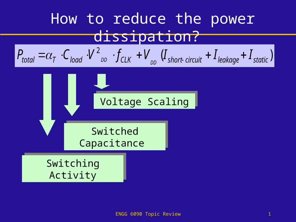
how to reduce the power dissipation?
DESCRIPTION
How to reduce the power dissipation?. Voltage Scaling. Switched Capacitance. Switching Activity. Low-Power Design Through Voltage Scaling. Different from constant-field scaling (Full Scaling). - PowerPoint PPT PresentationTRANSCRIPT
ENGG 6090 Topic Review 1
How to reduce the power dissipation?
)(2staticleakagecircuitshortCLKloadTtotal IIIVfVCP
DDDD
Switching ActivitySwitching Activity
Switched Capacitance Switched Capacitance
Voltage ScalingVoltage Scaling
ENGG 6090 Topic Review 2
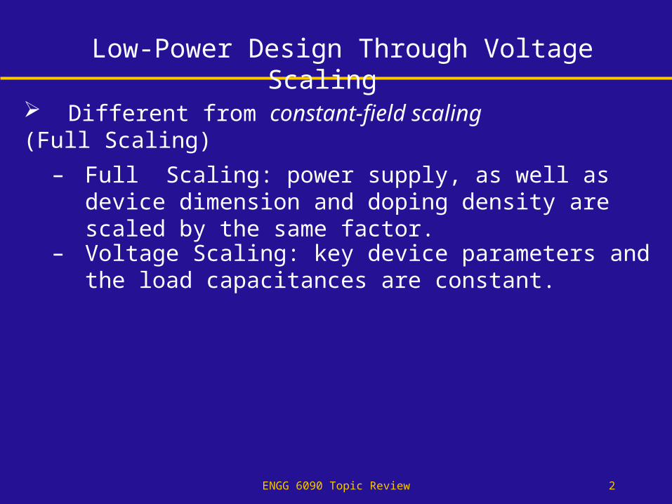
Low-Power Design Through Voltage Scaling
Different from constant-field scaling (Full Scaling)
– Full Scaling: power supply, as well as device dimension and doping density are scaled by the same factor.
– Voltage Scaling: key device parameters and the load capacitances are constant.
ENGG 6090 Topic Review 3
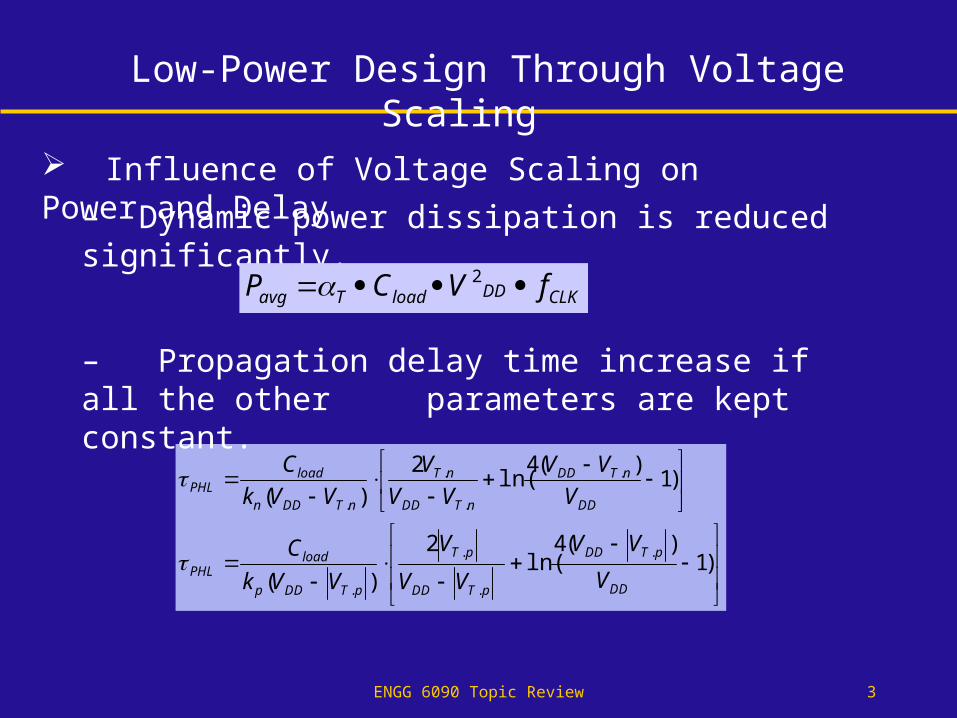
Influence of Voltage Scaling on Power and Delay
– Dynamic power dissipation is reduced significantly.
CLKDDloadTavg fVCP 2
)1)(4
ln(2
)(
)1)(4
ln(2
)(
.
.
.
.
.
.
.
.
DD
pTDD
pTDD
pT
pTDDp
loadPHL
DD
nTDD
nTDD
nT
nTDDn
loadPHL
V
VV
VV
V
VVk
C
V
VV
VV
V
VVk
C
– Propagation delay time increase if all the other parameters are kept constant.
Low-Power Design Through Voltage Scaling
ENGG 6090 Topic Review 4
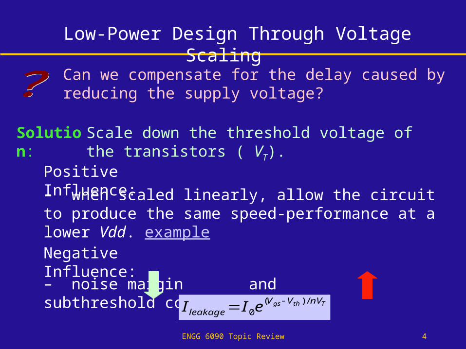
Can we compensate for the delay caused by reducing the supply voltage?
Solution: Scale down the threshold voltage of the transistors ( VT).
– when scaled linearly, allow the circuit to produce the same speed-performance at a lower Vdd. example
Positive Influence:
– noise margin and subthreshold conduction.
Negative Influence:
Low-Power Design Through Voltage Scaling
Tthgs nVVVleakage eII /)(
0
ENGG 6090 Topic Review 5
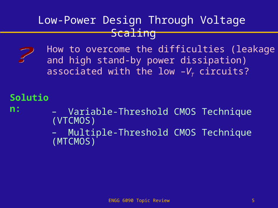
Solution:
– Variable-Threshold CMOS Technique (VTCMOS)
How to overcome the difficulties (leakage and high stand-by power dissipation) associated with the low –VT circuits?
Low-Power Design Through Voltage Scaling
– Multiple-Threshold CMOS Technique (MTCMOS)
ENGG 6090 Topic Review 6
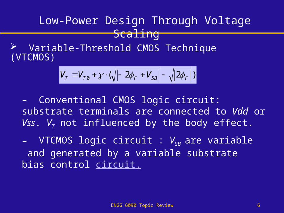
Variable-Threshold CMOS Technique (VTCMOS)
Low-Power Design Through Voltage Scaling
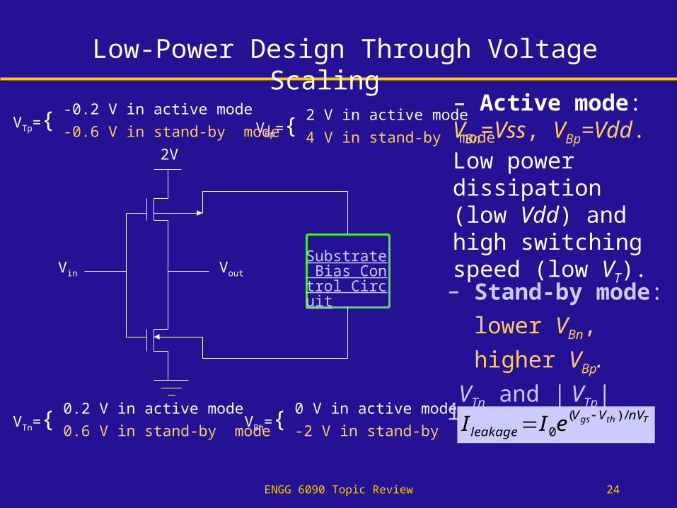
– Conventional CMOS logic circuit: substrate terminals are connected to Vdd or Vss. VT not influenced by the body effect.
)22(0 FSBFTT VVV
– VTCMOS logic circuit : VSB are variable and generated by a variable substrate bias control circuit.
ENGG 6090 Topic Review 7
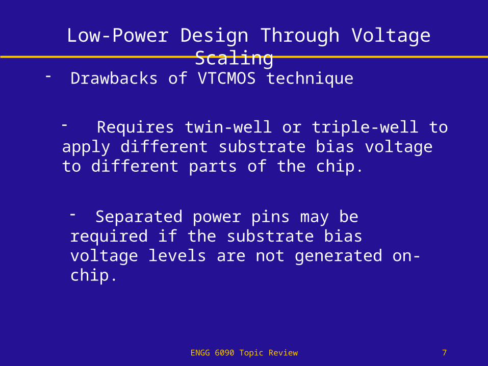
Requires twin-well or triple-well to apply different substrate bias voltage to different parts of the chip.
Low-Power Design Through Voltage Scaling
Separated power pins may be required if the substrate bias voltage levels are not generated on-chip.
Drawbacks of VTCMOS technique
ENGG 6090 Topic Review 8
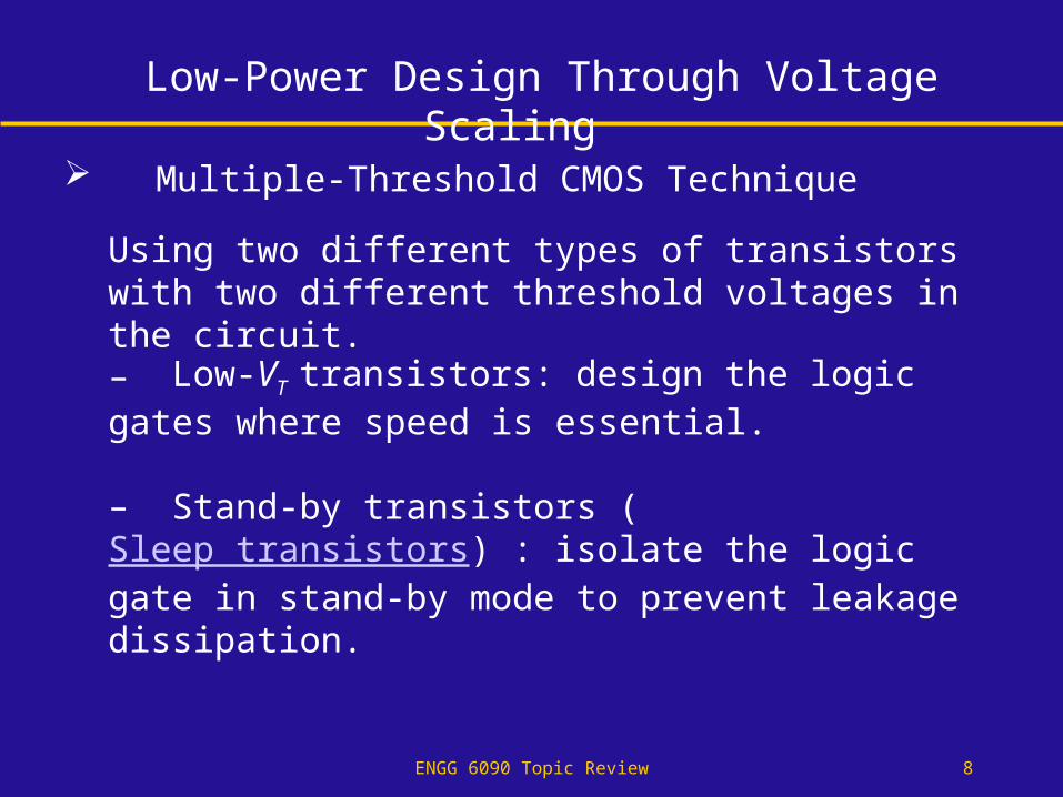
– Low-VT transistors: design the logic gates where speed is essential.
Multiple-Threshold CMOS Technique
Using two different types of transistors with two different threshold voltages in the circuit.
Low-Power Design Through Voltage Scaling
– Stand-by transistors (Sleep transistors) : isolate the logic gate in stand-by mode to prevent leakage dissipation.
ENGG 6090 Topic Review 9
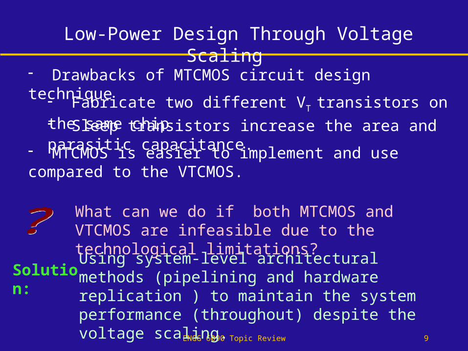
Drawbacks of MTCMOS circuit design technique
Solution:Using system-level architectural methods (pipelining and hardware replication ) to maintain the system performance (throughout) despite the voltage scaling.
Low-Power Design Through Voltage Scaling
Fabricate two different VT transistors on the same chip Sleep transistors increase the area and parasitic capacitance.
MTCMOS is easier to implement and use compared to the VTCMOS.
What can we do if both MTCMOS and VTCMOS are infeasible due to the technological limitations?
ENGG 6090 Topic Review 10
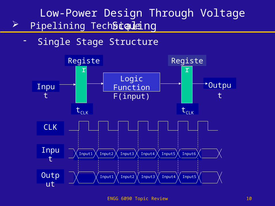
tCLKtCLK
Input Output
Register Register
Logic FunctionF(input)
Input6Input5Input4Input3Input2Input1Input
Output
CLK
Input5Input4Input3Input2Input1
Single Stage Structure
Low-Power Design Through Voltage Scaling Pipelining Technique
ENGG 6090 Topic Review 11
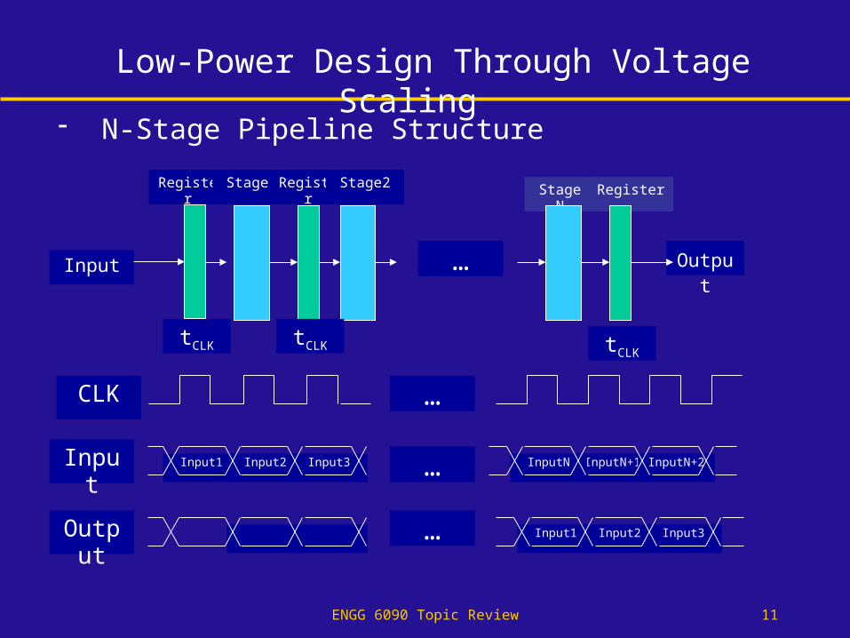
N-Stage Pipeline Structure
Register
tCLK
Input Output
Register Stage NStage1
…
Register Stage2
tCLK tCLK
CLK …
InputN+1InputN InputN+2Input3Input2Input1Input
Input2Input1 Input3Output …
…
Low-Power Design Through Voltage Scaling
ENGG 6090 Topic Review 12
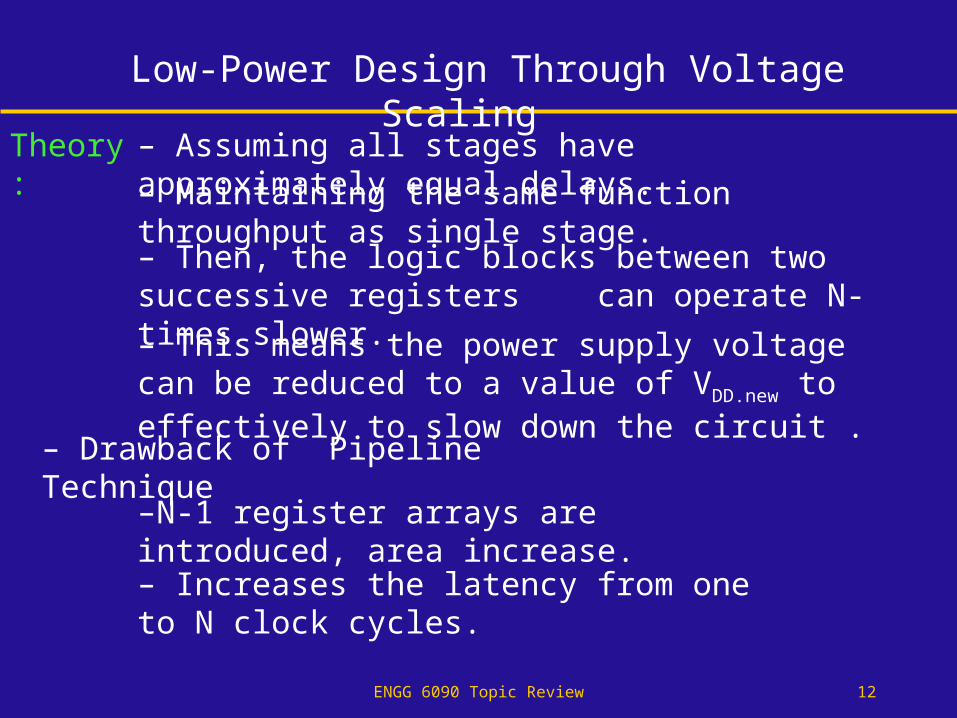
Theory:
Low-Power Design Through Voltage Scaling
– Drawback of Pipeline Technique
–N-1 register arrays are introduced, area increase.
– Increases the latency from one to N clock cycles.
– Assuming all stages have approximately equal delays.
– Maintaining the same function throughput as single stage.
– This means the power supply voltage can be reduced to a value of VDD.new to effectively to slow down the circuit .
– Then, the logic blocks between two successive registers can operate N-times slower.
ENGG 6090 Topic Review 13
Low-Power Design Through Voltage Scaling
…
…
…
…
…
CLK
Input2Input1 InputN+1InputNInput
CLK_1
CLK_2
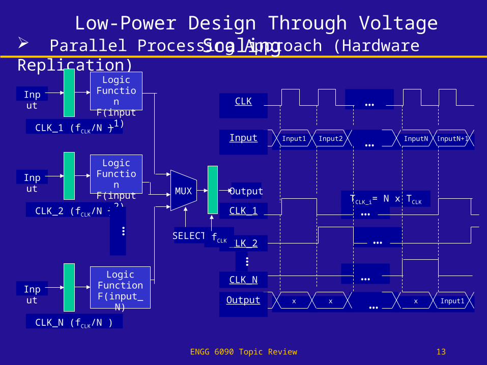
TCLK_i= N x TCLK
…
…xx Input1xOutput
CLK_N
Parallel Processing Approach (Hardware Replication)
MUX
SELECT fCLK
Output
CLK_1 (fCLK/N )
Input
Logic Function
F(input_1)
CLK_2 (fCLK/N )
Input
Logic Function
F(input_2)
CLK_N (fCLK/N )
Input
Logic Function
F(input_N)
…
ENGG 6090 Topic Review 14
Low-Power Design Through Voltage Scaling
Theory:
– Drawback of Hardware Replication
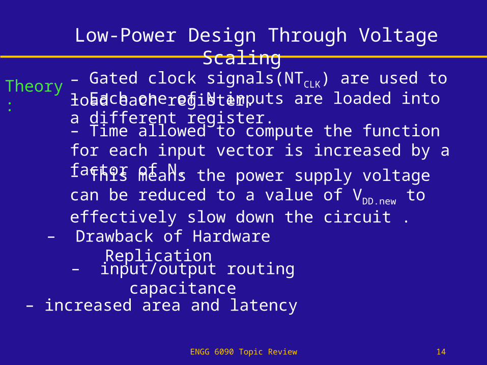
– Gated clock signals(NTCLK) are used to load each register.– Each one of N inputs are loaded into a different register.
– This means the power supply voltage can be reduced to a value of VDD.new to effectively slow down the circuit .
– Time allowed to compute the function for each input vector is increased by a factor of N.
– increased area and latency
– input/output routing capacitance
ENGG 6090 Topic Review 15
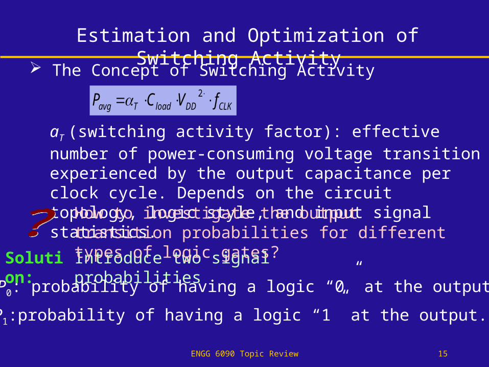
The Concept of Switching Activity
CLKDDloadTavg fVCP 2
aT (switching activity factor): effective number of power-consuming voltage transition experienced by the output capacitance per clock cycle. Depends on the circuit topology, logic style, and input signal statistics.
Solution: Introduce two signal probabilities
– P1:probability of having a logic “1” at the output. (P1=1-P0)
– P0: probability of having a logic “0” at the output.
Estimation and Optimization of Switching Activity
How to investigate the output transition probabilities for different types of logic gates?
ENGG 6090 Topic Review 16
Estimation and Optimization of Switching Activity
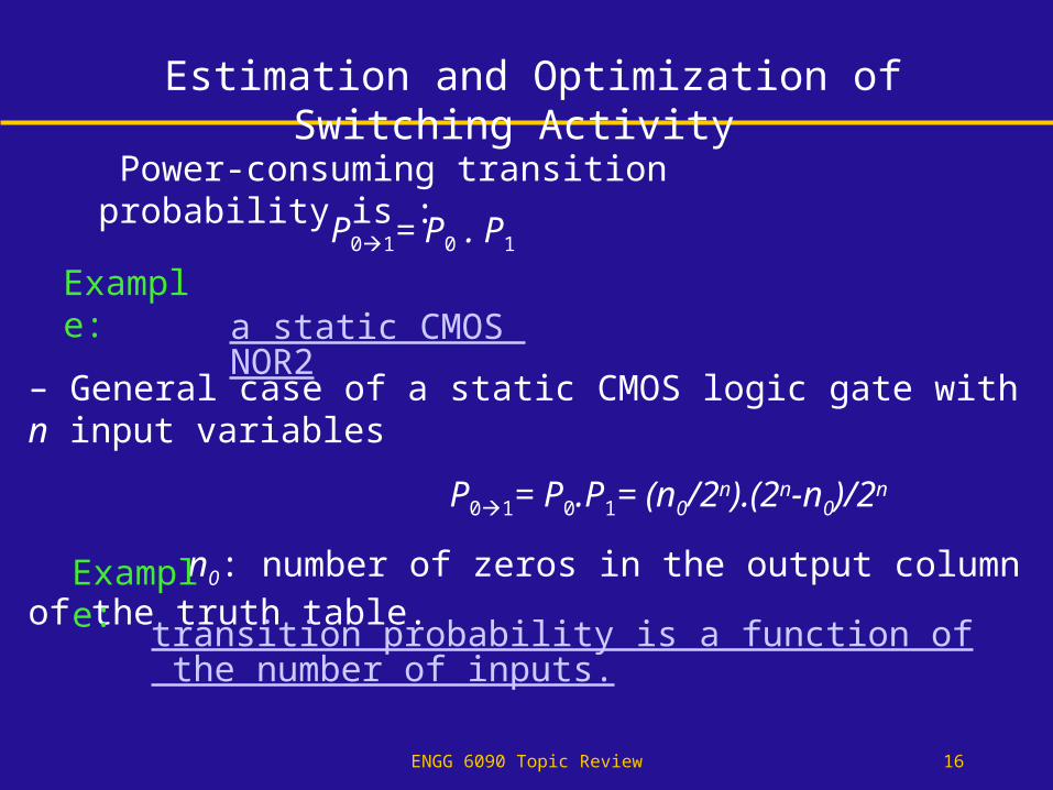
a static CMOS NOR2
– General case of a static CMOS logic gate with n input variables
P01= P0.P1= (n0/2n).(2n-n0)/2n
n0: number of zeros in the output column of the truth table.
Example:
transition probability is a function of the number of inputs.
Power-consuming transition probability is :
Example:
P01= P0 . P1
ENGG 6090 Topic Review 17
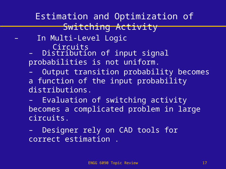
– In Multi-Level Logic Circuits
Estimation and Optimization of Switching Activity
– Distribution of input signal probabilities is not uniform.
– Evaluation of switching activity becomes a complicated problem in large circuits.
– Designer rely on CAD tools for correct estimation .
– Output transition probability becomes a function of the input probability distributions.
ENGG 6090 Topic Review 18
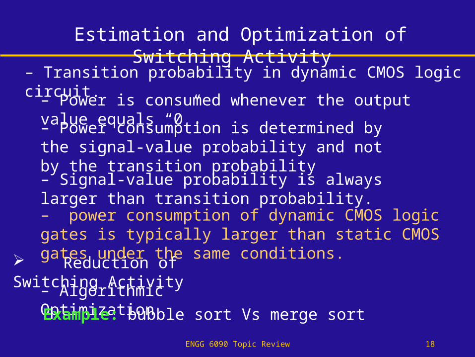
– Transition probability in dynamic CMOS logic circuit.
– Power is consumed whenever the output value equals “0”.
Reduction of Switching Activity
bubble sort Vs merge sort
Estimation and Optimization of Switching Activity
– power consumption of dynamic CMOS logic gates is typically larger than static CMOS gates under the same conditions.
– Signal-value probability is always larger than transition probability.
– Power consumption is determined by the signal-value probability and not by the transition probability
– Algorithmic Optimization
Example:
ENGG 6090 Topic Review 19
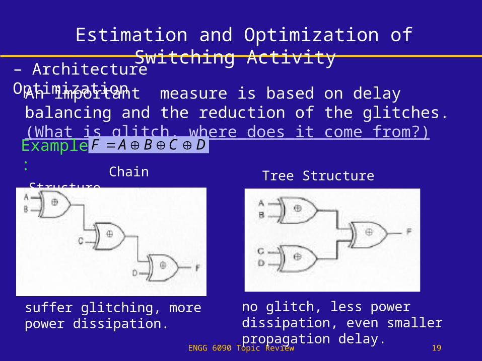
– Architecture Optimization
An important measure is based on delay balancing and the reduction of the glitches. (What is glitch, where does it come from?)
Example: DCBAF
Chain Structure
suffer glitching, more power dissipation.
Estimation and Optimization of Switching Activity
no glitch, less power dissipation, even smaller propagation delay.
Tree Structure
ENGG 6090 Topic Review 20
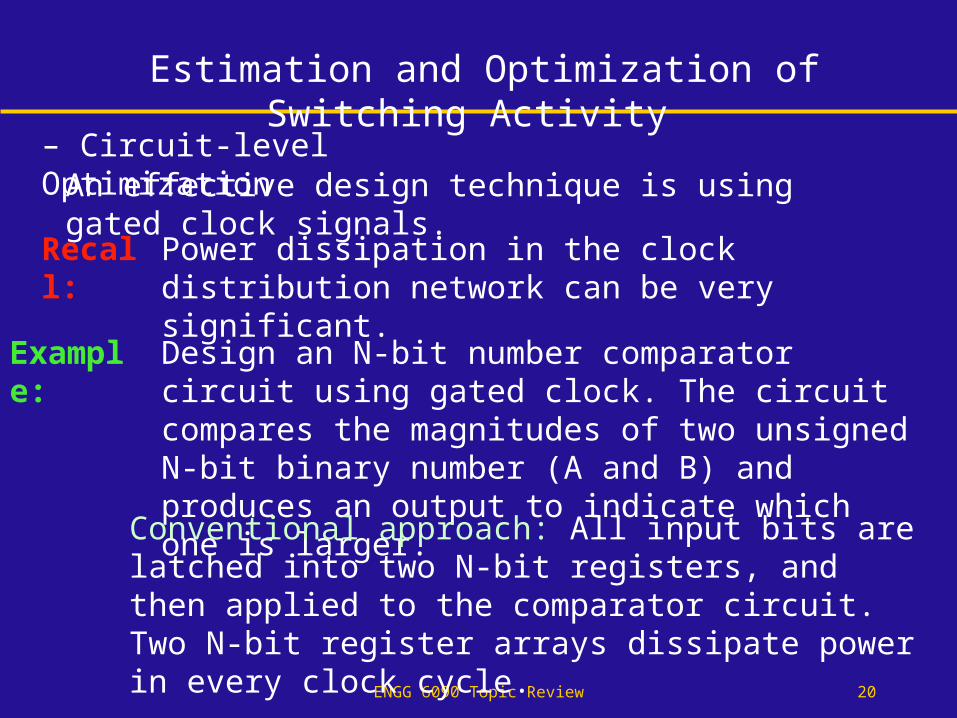
Power dissipation in the clock distribution network can be very significant.
– Circuit-level Optimization An effective design technique is using gated clock signals.
Recall:
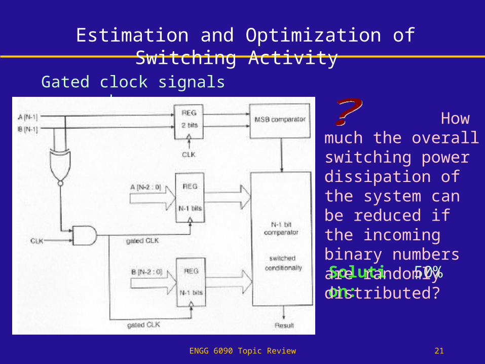
Example: Design an N-bit number comparator circuit using gated clock. The circuit compares the magnitudes of two unsigned N-bit binary number (A and B) and produces an output to indicate which one is larger.
Estimation and Optimization of Switching Activity
Conventional approach: All input bits are latched into two N-bit registers, and then applied to the comparator circuit. Two N-bit register arrays dissipate power in every clock cycle.
ENGG 6090 Topic Review 21
Gated clock signals approach:
Solution:
Estimation and Optimization of Switching Activity
50%
How much the overall switching power dissipation of the system can be reduced if the incoming binary numbers are randomly distributed?
ENGG 6090 Topic Review 22
Welcome Shaw back!
ENGG 6090 Topic Review 23
Low-Power Design Through Voltage Scaling
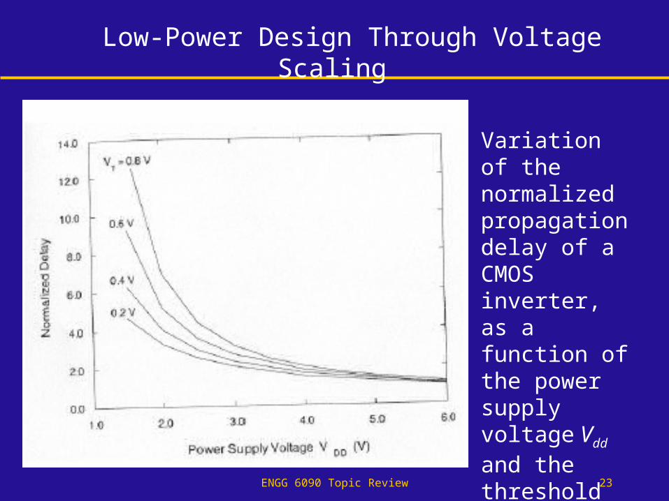
Variation of the normalized propagation delay of a CMOS inverter, as a function of the power supply voltage Vdd and the threshold voltage VT.
ENGG 6090 Topic Review 24
Vin Vout
2V
Substrate Bias Control Circuit
VTn={
VTp={
VBn={0 V in active mode0.2 V in active mode
VBp={2 V in active mode-0.2 V in active mode – Active mode:
VBn=Vss, VBp=Vdd. Low power dissipation (low Vdd) and high switching speed (low VT).
-2 V in stand-by mode0.6 V in stand-by mode
4 V in stand-by mode-0.6 V in stand-by mode
– Stand-by mode:
lower VBn,
higher VBp.
VTn and | VTp| increase. Tthgs nVVV
leakage eII /)(0
Low-Power Design Through Voltage Scaling
ENGG 6090 Topic Review 25
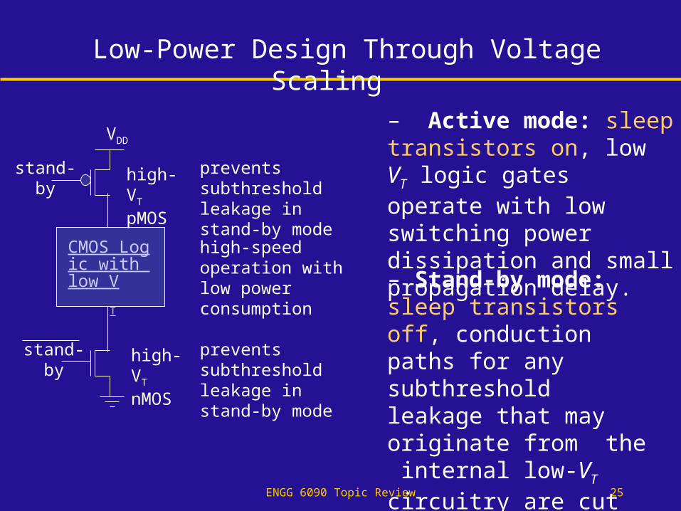
high-speed operation with low power consumption
prevents subthreshold leakage in stand-by mode
prevents subthreshold leakage in stand-by mode
CMOS Logic with low V
T
VDD
high- VT pMOS
stand-by
high- VT nMOS
stand-by
– Active mode: sleep transistors on, low VT logic gates operate with low switching power dissipation and small propagation delay.
– Stand-by mode: sleep transistors off, conduction paths for any subthreshold leakage that may originate from the internal low-VT circuitry are cut off.
Low-Power Design Through Voltage Scaling
ENGG 6090 Topic Review 26
Estimation and Optimization of Switching Activity
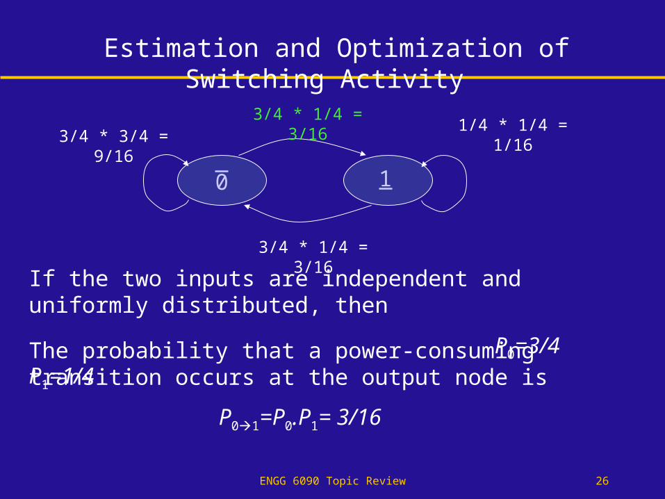
0
1
3/4 * 1/4 = 3/161/4 * 1/4 = 1/16
3/4 * 3/4 = 9/16
3/4 * 1/4 = 3/16
If the two inputs are independent and uniformly distributed, then
P0=3/4 P1=1/4
P01=P0.P1= 3/16
The probability that a power-consuming transition occurs at the output node is
ENGG 6090 Topic Review 27
Estimation and Optimization of Switching Activity
2 3 4 5 6 7 8
0.00
0.05
0.10
0.15
0.20
0.25
0.30
Number of Inputs
Out
put T
rans
itio
n P
roba
bili
ty
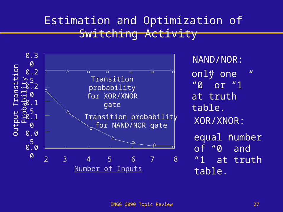
Transition probabilityfor NAND/NOR gate
Transition probability
for XOR/XNOR gate
NAND/NOR:
only one “0” or “1” at truth table.
XOR/XNOR:
equal number of “0” and “1” at truth table.
ENGG 6090 Topic Review 28
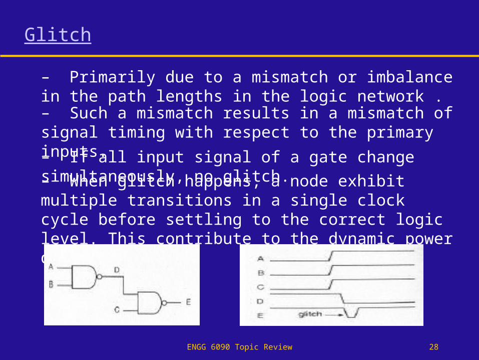
Glitch
– Primarily due to a mismatch or imbalance in the path lengths in the logic network .– Such a mismatch results in a mismatch of signal timing with respect to the primary inputs.
– If all input signal of a gate change simultaneously, no glitch.
– When glitch happens, a node exhibit multiple transitions in a single clock cycle before settling to the correct logic level. This contribute to the dynamic power dissipation.