hir1 ch09 photonics - ieee · 2019-10-03 · faced in packaging electronic ics, with the added...
TRANSCRIPT
2019 Edition
Chapter 9: Integrated Photonics
http://eps.ieee.org/hir
We acknowledge with gratitude the use of material and figures in this Roadmap that are excerpted from original sources. Figures & tables should be re-used only with the permission of the original source.
The HIR is devised and intended for technology assessment only and is without regard to any commercial considerations pertaining to individual products or equipment.
October, 2019 Table of Contents
HIR Version 1.0 (eps.ieee.org/hir) Page ii Heterogeneous Integration Roadmap
Table of Contents CHAPTER 1: HETEROGENEOUS INTEGRATION ROADMAP: OVERVIEW .......................................................................... 1
CHAPTER 2: HIGH PERFORMANCE COMPUTING AND DATA CENTERS ............................................................................. 1
CHAPTER 3: THE INTERNET OF THINGS (IOT) .................................................................................................................. 1
CHAPTER 4: MEDICAL, HEALTH & WEARABLES ............................................................................................................... 1
CHAPTER 5: AUTOMOTIVE ............................................................................................................................................ 1
CHAPTER 6: AEROSPACE AND DEFENSE ......................................................................................................................... 1
CHAPTER 7: MOBILE ...................................................................................................................................................... 1
CHAPTER 8: SINGLE CHIP AND MULTI CHIP INTEGRATION .............................................................................................. 1
CHAPTER 9: INTEGRATED PHOTONICS ........................................................................................................................... 1
CHAPTER 10: INTEGRATED POWER ELECTRONICS .......................................................................................................... 1
CHAPTER 11: MEMS AND SENSOR INTEGRATION ........................................................................................................... 1
CHAPTER 12: 5G COMMUNICATIONS ............................................................................................................................. 1
CHAPTER 13: CO DESIGN FOR HETEROGENEOUS INTEGRATION ..................................................................................... 1
CHAPTER 14: MODELING AND SIMULATION .................................................................................................................. 1
CHAPTER 15: MATERIALS AND EMERGING RESEARCH MATERIALS ................................................................................. 1
CHAPTER 16: EMERGING RESEARCH DEVICES ................................................................................................................ 1
CHAPTER 17: TEST TECHNOLOGY ................................................................................................................................... 1
CHAPTER 18: SUPPLY CHAIN .......................................................................................................................................... 1
CHAPTER 19: SECURITY ................................................................................................................................................. 1
CHAPTER 20: THERMAL ................................................................................................................................................. 1
CHAPTER 21: SIP AND MODULE SYSTEM INTEGRATION ................................................................................................. 1
CHAPTER 22: INTERCONNECTS FOR 2D AND 3D ARCHITECTURES ................................................................................... 1
CHAPTER 23: WAFER‐LEVEL PACKAGING (WLP) ............................................................................................................. 1
To download additional chapters, please visit
http://eps.ieee.org/hir
October, 2019 Integrated Photonics
HIR version 1.0 (eps.ieee.org/hir) Chapter 9, Page 1 Heterogeneous Integration Roadmap
Chapter 9: Integrated Photonics
This chapter is in preparation, and will be integrated into the Roadmap at Version 1.1, planned for the end of 2019.
In its place is the following summary and a series of slides giving the current status of integrated photonics and some information that is relevant to the progress needed over the next 10 to 15 years.
Executive Summary The global network requirements are changing with the rise of the internet of things (IoT) and the migration to the
cloud of data, logic and applications. These changing requirements must be accommodated while maintaining the pace of progress in size, cost and power per function that we have enjoyed for more than 50 years. This progress was based primarily on the benefits of Moore’s Law scaling of CMOS electronics. The introduction of photonics into the transmission, processing and even the generation of data through optical-based sensors is a key enabling factor for continued progress in these areas as we reach the limits of the physics, and the benefits of Moore’s Law scaling slow.
There will be many specific challenges in integrating the benefits of photonics into the fabric of the global network. The solutions, however, cannot come from just the packaging of photonic components. The co-packaging of electronics, photonics and plasmonics will be required to address these substantial new challenges in order to meet the expanding requirement for higher performance, higher reliability, increased security, lower latency and continued decrease in cost per function. The packaging of photonic integrated circuits (PICs) will face the same challenges faced in packaging electronic ICs, with the added complexity of integrating both active and passive photonic elements as well as the necessary electronics. Wherever possible industry must adopt and adapt the packaging technologies developed for electronics to decrease cost and time-to-market for packaging of individual PIC circuits and incorporating PIC circuits and other photonic components into the complex 3D SiP through heterogeneous integration.
October, 2019 Integrated Photonics
HIR version 1.0 (eps.ieee.org/hir) Chapter 9, Page 2 Heterogeneous Integration Roadmap
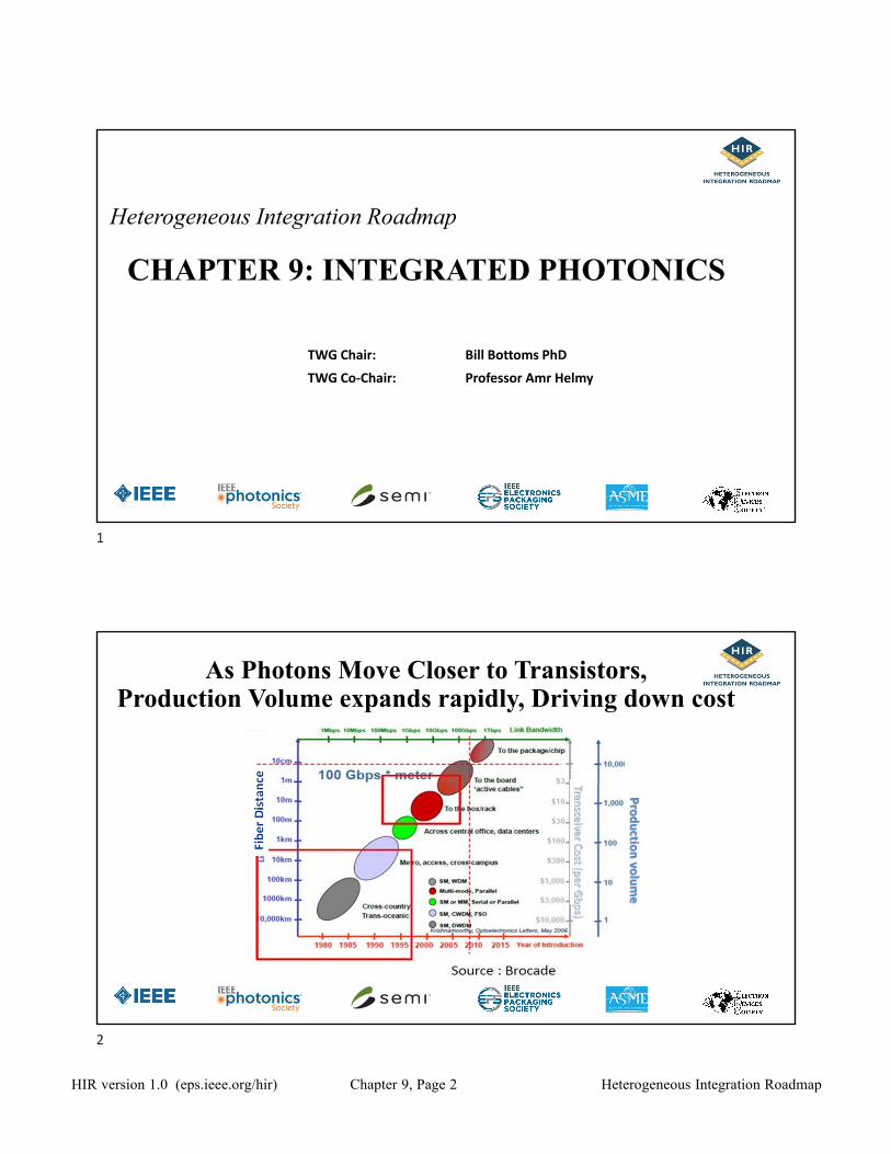
TWG Chair: Bill Bottoms PhD
TWG Co‐Chair: Professor Amr Helmy
Heterogeneous Integration Roadmap
CHAPTER 9: INTEGRATED PHOTONICS
As Photons Move Closer to Transistors, Production Volume expands rapidly, Driving down cost
1
2
October, 2019 Integrated Photonics
HIR version 1.0 (eps.ieee.org/hir) Chapter 9, Page 3 Heterogeneous Integration Roadmap
PACKAGING PHOTONIC DEVICESThere are a large number of devices involving photons which share the common requirement of providing a photon path either into or out of a system, or both. They include:
• Light emitting diodes (LEDs)• Laser diodes• Plasmonic photon emitters • Photonic Integrated circuits (PICs)• MEMS optical switching devices• Camera modules• Optical modulators• Active optical cables• E to O and O to E converters• Optical sensors (photo diodes and other types)• WDM multiplexers and de‐multiplexers
Many have unique thermal, electrical, and mechanical characteristics that will require specialized materials and system integration (packaging) processes and
equipment
A Selection of Emerging Integrated Photonic Solutions
Addressing various
Heterogenous Integration Challenges
3
4
October, 2019 Integrated Photonics
HIR version 1.0 (eps.ieee.org/hir) Chapter 9, Page 4 Heterogeneous Integration Roadmap
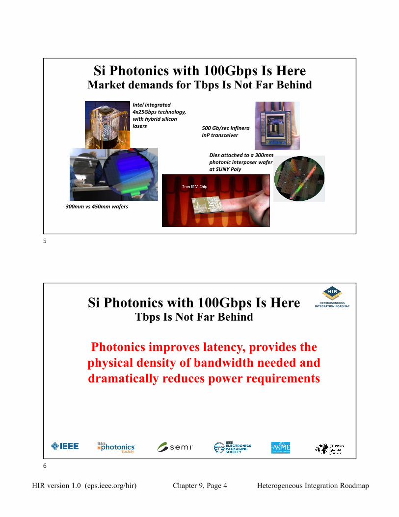
Si Photonics with 100Gbps Is Here Market demands for Tbps Is Not Far Behind
300mm vs 450mm wafers
500 Gb/sec Infinera InP transceiver
Intel integrated 4x25Gbps technology, with hybrid silicon lasers
Dies attached to a 300mm photonic interposer waferat SUNY Poly
Si Photonics with 100Gbps Is Here Tbps Is Not Far Behind
Photonics improves latency, provides the physical density of bandwidth needed and dramatically reduces power requirements
5
6
October, 2019 Integrated Photonics
HIR version 1.0 (eps.ieee.org/hir) Chapter 9, Page 5 Heterogeneous Integration Roadmap
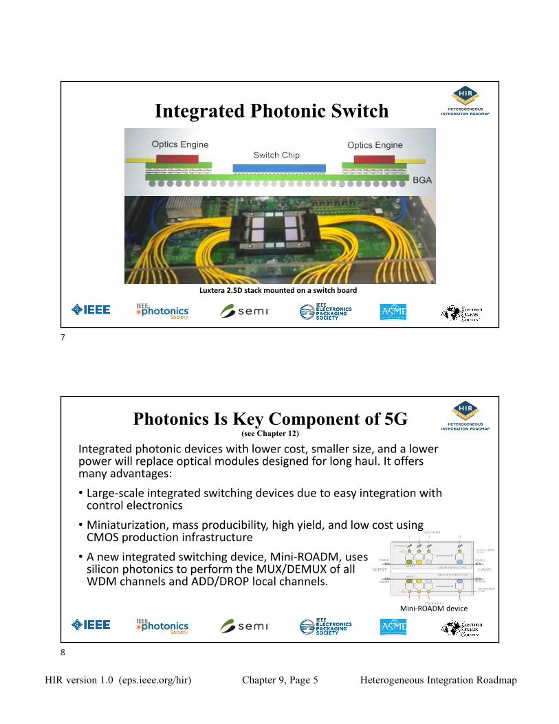
Luxtera 2.5D stack mounted on a switch board
Integrated Photonic Switch
Photonics Is Key Component of 5G(see Chapter 12)
Integrated photonic devices with lower cost, smaller size, and a lower power will replace optical modules designed for long haul. It offers many advantages:• Large‐scale integrated switching devices due to easy integration with control electronics
• Miniaturization, mass producibility, high yield, and low cost using CMOS production infrastructure
• A new integrated switching device, Mini‐ROADM, uses silicon photonics to perform the MUX/DEMUX of all WDM channels and ADD/DROP local channels.
Mini‐ROADM device
7
8
October, 2019 Integrated Photonics
HIR version 1.0 (eps.ieee.org/hir) Chapter 9, Page 6 Heterogeneous Integration Roadmap
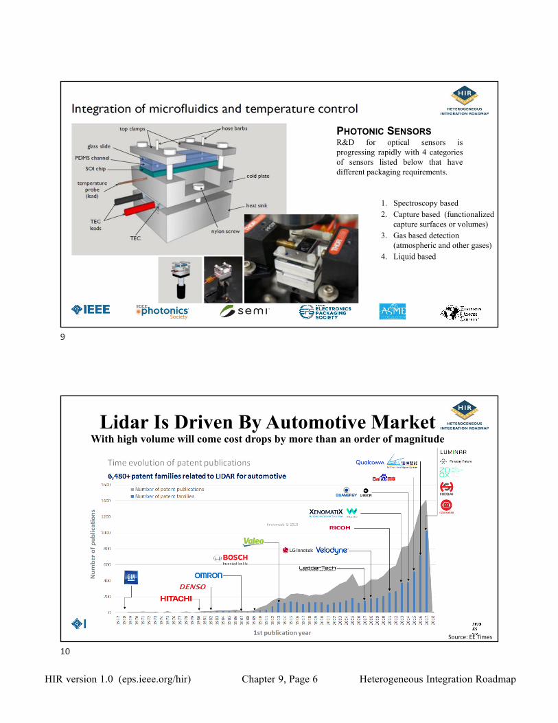
PHOTONIC SENSORSR&D for optical sensors isprogressing rapidly with 4 categoriesof sensors listed below that havedifferent packaging requirements.
1. Spectroscopy based2. Capture based (functionalized
capture surfaces or volumes) 3. Gas based detection
(atmospheric and other gases)4. Liquid based
Lidar Is Driven By Automotive Market With high volume will come cost drops by more than an order of magnitude
Source: EE Times
9
10
October, 2019 Integrated Photonics
HIR version 1.0 (eps.ieee.org/hir) Chapter 9, Page 7 Heterogeneous Integration Roadmap
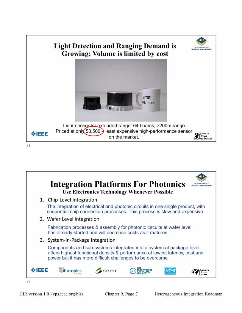
Light Detection and Ranging Demand is Growing; Volume is limited by cost
Lidar sensor for extended range: 64 beams, >200m rangePriced at only $3,500 – least expensive high-performance sensor
on the market. Source: Ouster
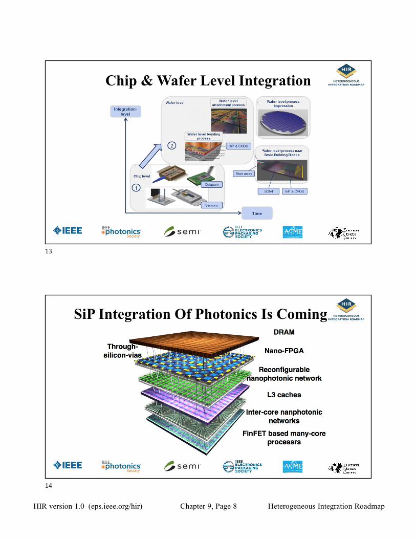
Integration Platforms For PhotonicsUse Electronics Technology Whenever Possible
1. Chip‐Level IntegrationThe integration of electrical and photonic circuits in one single product, with sequential chip connection processes. This process is slow and expensive.
2. Wafer Level IntegrationFabrication processes & assembly for photonic circuits at wafer level has already started and will decrease costs as it matures.
3. System‐in‐Package integrationComponents and sub-systems integrated into a system at package level offers highest functional density & performance at lowest latency, cost and power but it has more difficult challenges to be overcome
11
12
October, 2019 Integrated Photonics
HIR version 1.0 (eps.ieee.org/hir) Chapter 9, Page 8 Heterogeneous Integration Roadmap
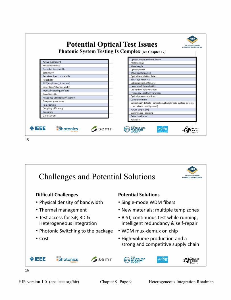
Chip & Wafer Level Integration
SiP Integration Of Photonics Is Coming
13
14
October, 2019 Integrated Photonics
HIR version 1.0 (eps.ieee.org/hir) Chapter 9, Page 9 Heterogeneous Integration Roadmap
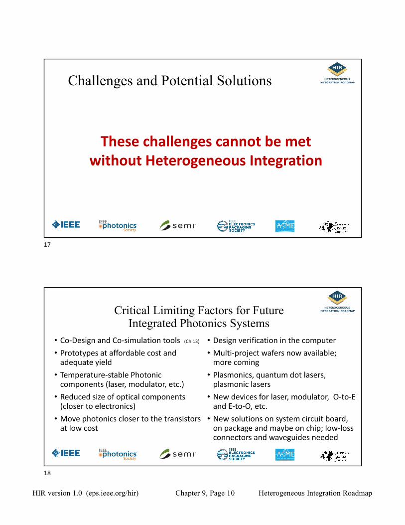
Optical Amplitude ModulationPolarizationsWavelengthOptical powerWavelength spacingOptical Modulation RateBER ‐ eye mask (4x)EYE(amplitued, jitter, etc)Laser lane/channel widthLasing threshold variationFrequency spectrum variationOptical power variationsCoherence timeOptical path defects ( optical coupling defects: surface defects: core defects misalignment)Power output (4x)System Loss ‐ couplingExtinction RatioReliability
Potential Optical Test IssuesPhotonic System Testing Is Complex (see Chapter 17)
Active AlignmentResponsivenessDetector bandwidthSensitivityReceiver Spectrum widthReliabilityEYE(amplitued, jitter, etc)Laser lane/channel width optical coupling defectsSensitivity (4x)Response time (delay/latency)Frequency responsePolarizationCoupling efficiencyCrosstalkDark current
Challenges and Potential Solutions
Difficult Challenges• Physical density of bandwidth • Thermal management• Test access for SiP, 3D & Heterogeneous integration
• Photonic Switching to the package• Cost
Potential Solutions• Single‐mode WDM fibers• New materials; multiple temp zones• BIST, continuous test while running, intelligent redundancy & self‐repair
• WDM mux‐demux on chip• High‐volume production and a strong and competitive supply chain
15
16
October, 2019 Integrated Photonics
HIR version 1.0 (eps.ieee.org/hir) Chapter 9, Page 10 Heterogeneous Integration Roadmap
Challenges and Potential Solutions
These challenges cannot be met without Heterogeneous Integration
Critical Limiting Factors for Future Integrated Photonics Systems
• Co‐Design and Co‐simulation tools (Ch 13)• Prototypes at affordable cost and adequate yield
• Temperature‐stable Photonic components (laser, modulator, etc.)
• Reduced size of optical components (closer to electronics)
• Move photonics closer to the transistors at low cost
• Design verification in the computer• Multi‐project wafers now available; more coming
• Plasmonics, quantum dot lasers, plasmonic lasers
• New devices for laser, modulator, O‐to‐E and E‐to‐O, etc.
• New solutions on system circuit board, on package and maybe on chip; low‐loss connectors and waveguides needed
17
18
October, 2019 Integrated Photonics
HIR version 1.0 (eps.ieee.org/hir) Chapter 9, Page 11 Heterogeneous Integration Roadmap
Many New Components / Technologies For Integrated Photonics
with New Capabilities are in an
Advanced State of Development
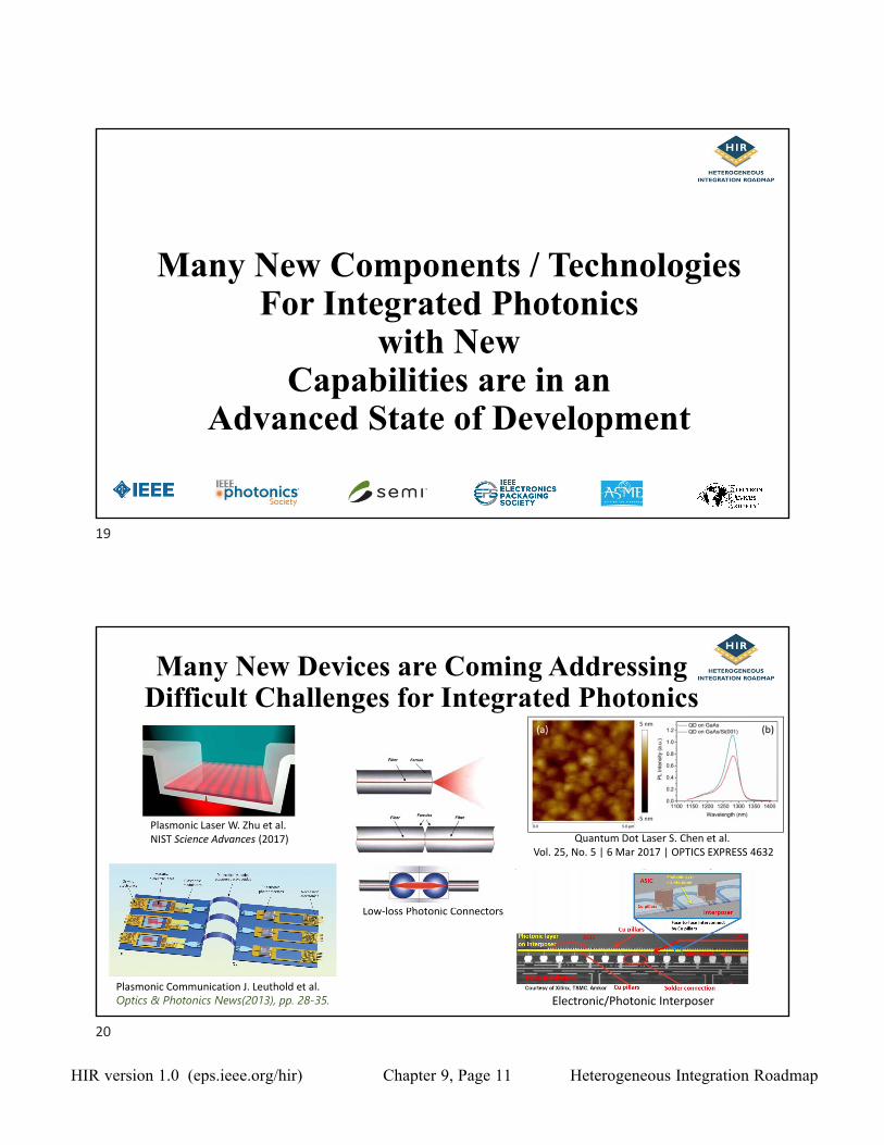
Many New Devices are Coming Addressing Difficult Challenges for Integrated Photonics
Plasmonic Communication J. Leuthold et al.Optics & Photonics News(2013), pp. 28-35.
Quantum Dot Laser S. Chen et al. Vol. 25, No. 5 | 6 Mar 2017 | OPTICS EXPRESS 4632
Low‐loss Photonic Connectors
Electronic/Photonic Interposer
Plasmonic Laser W. Zhu et al. NIST Science Advances (2017)
19
20
October, 2019 Integrated Photonics
HIR version 1.0 (eps.ieee.org/hir) Chapter 9, Page 12 Heterogeneous Integration Roadmap
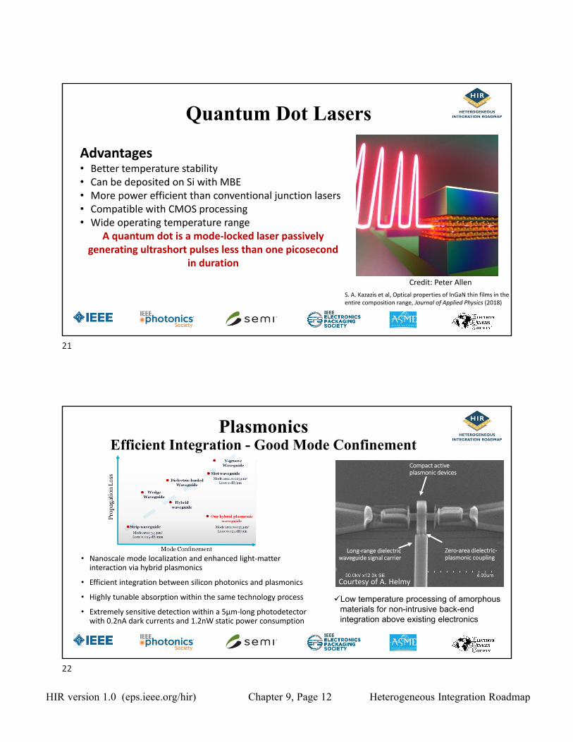
Quantum Dot Lasers
S. A. Kazazis et al, Optical properties of InGaN thin films in the entire composition range, Journal of Applied Physics (2018)
Advantages• Better temperature stability• Can be deposited on Si with MBE• More power efficient than conventional junction lasers• Compatible with CMOS processing• Wide operating temperature range
A quantum dot is a mode‐locked laser passively generating ultrashort pulses less than one picosecond
in duration
Credit: Peter Allen
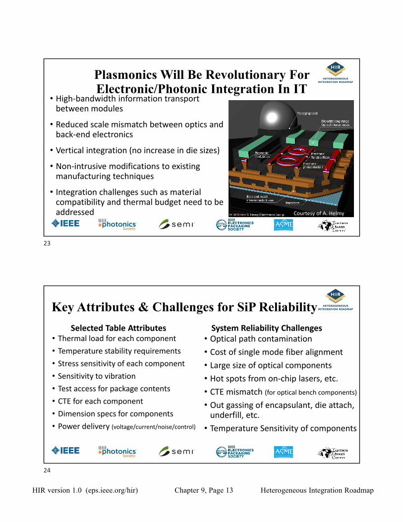
PlasmonicsEfficient Integration - Good Mode Confinement
• Nanoscale mode localization and enhanced light‐matter interaction via hybrid plasmonics
• Efficient integration between silicon photonics and plasmonics
• Highly tunable absorption within the same technology process
• Extremely sensitive detection within a 5µm‐long photodetector with 0.2nA dark currents and 1.2nW static power consumption
Long‐range dielectric waveguide signal carrier
Compact active plasmonic devices
Zero‐area dielectric‐plasmonic coupling
9Low temperature processing of amorphous materials for non-intrusive back-end integration above existing electronics
Courtesy of A. Helmy
21
22
October, 2019 Integrated Photonics
HIR version 1.0 (eps.ieee.org/hir) Chapter 9, Page 13 Heterogeneous Integration Roadmap
• High‐bandwidth information transport between modules
• Reduced scale mismatch between optics and back‐end electronics
• Vertical integration (no increase in die sizes)
• Non‐intrusive modifications to existing manufacturing techniques
• Integration challenges such as material compatibility and thermal budget need to be addressed
BEOL OPTOELECTRONICSPlasmonics Will Be Revolutionary For Electronic/Photonic Integration In IT
Courtesy of A. Helmy
Key Attributes & Challenges for SiP Reliability
• Thermal load for each component• Temperature stability requirements• Stress sensitivity of each component• Sensitivity to vibration• Test access for package contents• CTE for each component• Dimension specs for components• Power delivery (voltage/current/noise/control)
• Optical path contamination• Cost of single mode fiber alignment• Large size of optical components• Hot spots from on‐chip lasers, etc.• CTE mismatch (for optical bench components)
• Out gassing of encapsulant, die attach, underfill, etc.
• Temperature Sensitivity of components
Selected Table Attributes System Reliability Challenges
23
24
October, 2019 Integrated Photonics
HIR version 1.0 (eps.ieee.org/hir) Chapter 9, Page 14 Heterogeneous Integration Roadmap
ConclusionIntegrated photonics will be a key enabler, delivering the low power, low cost, low latency and increased bandwidth density and performance required to meet the demands of the data and data traffic explosion that will continue rapid growth.The physical bandwidth density needed to support big data, data analytics, artificial intelligence and neuromorphic and quantum computing will be much greater, and photonics will continue to get closer to the logic supporting these emerging technologies for decades to come. This view of the future cannot be realized without increasing
performance and density in Integrated Photonics
25