hi–ps technique for mems fabrication
TRANSCRIPT
Sensors and Actuators A 115 (2004) 608–616
HI–PS technique for MEMS fabrication
M.O.S. Dantasa,∗, E. Galeazzoa, H.E.M. Peresa, F.J. Ramirez-Fernandeza, A. Errachidb
a Laboratório de Microeletronica, Universidade de São Paulo, Escola Politécnica, USP, Av. Prof. Luciano Gualberto,Trav. 3, 158, CEP 05508-900, Sensores Integrados e Microssistemas, SIM Group, São Paulo, SP, Brazil
b Laboratory of NanoBioEngineering, Barcelona Science Park, Barcelona, Spain
Received 22 September 2003; received in revised form 13 March 2004; accepted 27 March 2004Available online 18 May 2004
Abstract
This work presents the results obtained by mean of a promising procedure for silicon-based MEMS fabrication named hydrogen ionimplantation–porous silicon (HI–PS) technique. On this technique HI followed by adequate thermal annealing constitutes an effective“mask” for subsequent PS formation by usual anodization process [Sens. Actuators B 76 (2001) 343]. As this formation is isotropic undermasks borders, PS can be used as sacrificial layer in order to obtain silicon microstructures as sharp tips (diameter around 0.1�m andheight around 45�m) and thin membranes (around 1�m thick). Additionally, it is shown that membranes thickness can be controlled bythermal annealing time, so thickness up to 4�m can be obtained.© 2004 Elsevier B.V. All rights reserved.
Keywords: MEMS; Silicon tips; Silicon membranes; Porous silicon; Hydrogen ion implantation; Microelectrodes; Sacrificial layer
1. Introduction
The continual demand for sensors and control sys-tems in all areas has stimulated the development ofmicro-electro-mechanical systems (MEMS). For this pur-pose, many alternatives of materials and fabrication pro-cesses are applied and new alternatives are frequentlyexperienced. In general, integration between mechanicalmicrostructures and microelectronic circuits is preferreddue to advantages offered by the well established micro-electronic technology, such as batch process, miniaturiza-tion, low cost, fast response, low noise, and the possibilityto realize in situ signal processing. Moreover, silicon hasappropriated mechanical and electrical characteristics formicrostructures fabrication. In such way, it is importantthat materials and processes for fabrication of integratedmicrostructures be compatible with CMOS technology.
This work explores a new procedure for microstructuresfabrication reported in recent works[1–3]and here called hy-drogen ion implantation–porous silicon (HI–PS) technique.In this technique porous silicon is used as sacrificial layerunder geometries “masked” by hydrogen ion implantation
∗ Corresponding author. Tel.:+55-11-3091-5310;fax: +55-11-3091-5585.E-mail address: [email protected] (M.O.S. Dantas).URL: http://sim.lme.usp.br.
(or simply hydrogen implantation) followed by rapid ther-mal annealing (RTA).
PS is a sponge-like material usually obtained by electro-chemical anodization of crystalline silicon into HF solution.Due to its high specific area (around 400 m2/cm3) and highreactivity, PS can be applied as material for gas sensors[4,5].Due to the photoluminescence properties of PS at room tem-perature, PS is also a promising material for optoelectronicapplications[6,7]. Also, PS can be used as electrical andthermal isolation as well as sacrificial layer for microstruc-tures fabrication. For this application, there are some advan-tages on the usage of PS[8].
• PS obtaining is a simple and cheap fabrication process.• There is high CMOS compatibility.• Possibility of obtaining thick layers, about hundreds mi-
crometers.• No significant dependence on crystallographic orientation
of Si bulk.• Selectivity dependent on type and bulk doping.• Fast chemical reactions occur on PS surface, making etch-
ing easy and simple at room temperature.• It is possible to obtain surface or bulk micromachining.
In order to masking PS formation, anodization currentmust be blocked by some electrically isolated layer werePS is not desired. Usual choices are polysilicon over sili-con dioxide[9], silicon nitride[8] or even n-type doping (as
0924-4247/$ – see front matter © 2004 Elsevier B.V. All rights reserved.doi:10.1016/j.sna.2004.03.062
M.O.S. Dantas et al. / Sensors and Actuators A 115 (2004) 608–616 609
phosphorous) by ion implantation into p-type silicon sub-strates[10]. An alternative method is the combination ofhydrogen ion implantation into p-type silicon and RTA, thatcreates a stable high resistivity layer into silicon due to thesum of three factors[1].
• Damage of crystalline silicon lattice by the ion implanta-tion process.
• Neutralization of boron (the dopant in p-type silicon) bythe hydrogen (dopant passivation).
• RTA process induces H2 bubbles formation, which lowdiffusivity makes difficult the lattice rearrangement andfixing the high resistivity layer.
As reported in previous work[11], such “mask” for siliconanodization has many advantages
• It is an effective barrier against anodization current onundesirable regions.
• There is no time limitation for anodization process, sothick PS layers can be obtained.
• As the PS formation is isotropic bellow mask borders, asuperficial silicon layer can be obtained above PS layer.
• As the PS can be easily removed by diluted KOH at roomtemperature, a fast micromachining can be performed andsilicon membranes around 1�m thick can be obtained.
• Membranes have low mechanical stress.
Besides these advantages, one interesting characteristicstudied and explored in this work is that the thickness of thehigh resistivity layer can be raised by adding a conventionalthermal annealing (CTA) step after RTA[3].
This way, HI–PS technique is applied in this work to studythe fabrication of two important types of microstructuresuseful for MEMS: silicon membranes and silicon tips, withespecial attention to the possibility to control the membranethickness from CTA time.
Membranes are used in a large number of applicationssuch as pressure sensors, accelerometers, micropumps and
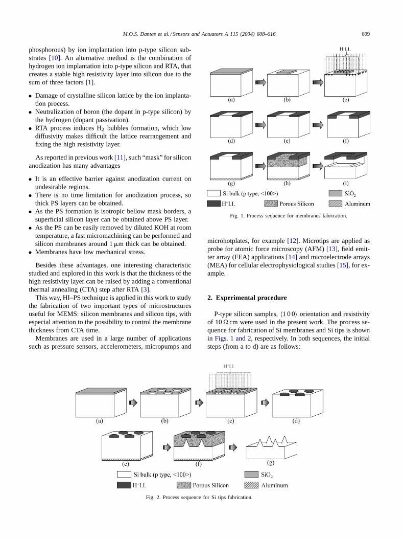
Fig. 2. Process sequence for Si tips fabrication.
Fig. 1. Process sequence for membranes fabrication.
microhotplates, for example[12]. Microtips are applied asprobe for atomic force microscopy (AFM)[13], field emit-ter array (FEA) applications[14] and microelectrode arrays(MEA) for cellular electrophysiological studies[15], for ex-ample.
2. Experimental procedure
P-type silicon samples,〈1 0 0〉 orientation and resistivityof 10� cm were used in the present work. The process se-quence for fabrication of Si membranes and Si tips is shownin Figs. 1 and 2, respectively. In both sequences, the initialsteps (from a to d) are as follows:

610 M.O.S. Dantas et al. / Sensors and Actuators A 115 (2004) 608–616
Fig. 3. Geometries applied on study of HI–PS technique for microstructures fabrication (a and b) stripes for CTA studies and (c) circles/squares for Sitips fabrication.
(1a/2a) Thermal growth of 1�m thickness silicon oxide(SiO2) as a barrier against the HI.
(1b/2b) Definition of regions (by lithography) in which H+is implanted.
(1c/2c) HI with energy of 50 keV and dose of 1×10¹⁶ H+/cm2.
(1d/2d) SiO2 etching.
Considering the processes described before, it is possi-ble to take two ways for microstructures fabrication, as pre-sented in the next paragraphs.
2.1. Si membranes fabrication
The way for obtaining Si membranes, as shown fromFig. 1e–i, is the following one
(1e) RTA with temperature of 450◦C, time of 5 min andargon environment to activate the H+ ion on Si. Thisstep results in a high resistivity layer about 1�m thick,which corresponds to Si membranes thickness if noCTA step is applied, as reported before[2].
(1f) CTA (T = 1200◦C, environment: O2 (t = 10 min) +N2 (t = 54 or 90 min)) to increase the thickness ofhigh resistivity layer after RTA process. The initial ox-idation step in CTA process is done to avoid possiblecontamination from the oven to the sample during thethermal annealing.
(1g) Aluminum (Al) evaporation to improve ohmic contactat the backside of Si bulk, followed by thermal process(T = 450◦C, environment: N2 (95%)/H2 (5%), t =30 min) to form Al/Si alloy.
(1h) PS formation on selective areas by anodization process(HF chemical solution (48% wt.), current density (J)of 20 mA/cm2 and process times of 20 min).
(1i) PS etching by diluted aqueous KOH (1% concentra-tion) at room temperature for obtaining microstruc-tures.
2.2. Si tips fabrication
The complementary steps for obtaining the Si tips, asshown fromFig. 2e–g, are described next.
(2e) Aluminum (Al) evaporation to form ohmic contact atthe backside of Si bulk, followed by RTA (rapid ther-mal annealing) with temperature of 450◦C, time of5 min and argon environment to activate the H+ ion onSi and to form Al/Si alloy.
(2f) PS formation on selective areas by anodization process(HF chemical solution (48% wt.), current density (J)of 20 mA/cm2 and different process time to promotelateral link of PS layers).
(2g) PS etching by diluted aqueous KOH (1% concentra-tion) at room temperature for Si Tip obtaining.
2.3. Mask geometries
Lithographic masks with “stripes” (for CTA studies,Fig. 3a and b) and circular/square geometries (for Si tipsstudies,Fig. 3c) were designed. The black regions inFig. 3are the regions with H+I.I., where PS is not desired. Thewhite ones are the PS formation regions. The masks de-signed explore the isotropic PS formation; this way, thePS layer will be formed under the HI region and afterthe removal of PS, only the HI regions remains as thinmembranes. In the mask for Si tips fabrication studies isimportant to emphasize that the designed geometries havedifferent dimensions of diameter (∅) and side (d) in thesame lithographic mask, thus, it is possible to explore theformation of different structures from a single anodizationprocess.
3. Results and discussion
3.1. Si membranes obtained by HI and RTA + CTAprocesses
Fig. 4 shows scanning electron microscopy (SEM)cross-section images of Si samples before and after PS hasbeen removed by etching in a diluted KOH solution. Thethickness of the remaining Si layer on the sample with HIand RTA processes is about 1�m Fig. 4a and b).
With and additional CTA step included in the process (of64 and 100 min as indicated inFig. 4) the remaining Si layershows thickness about 1.6�m Fig. 4c and d) and 1.9�mFig. 4e and f), respectively.

M.O.S. Dantas et al. / Sensors and Actuators A 115 (2004) 608–616 611
Fig. 4. Samples with HI, RTA and different conditions of CTA process: (a) only RTA process (T = 450◦C, t = 5 min) (b) the same sample after PSetching, proving that the remaining layer is silicon (c) RTA+CTA processes (T = 1200◦C, t = 64 min) before and (d) after the PS etching (e) RTA+CTAprocesses (T = 1200◦C, t = 100 min) before and (f) after the PS etching, where it is possible to see large irregularities at the Si remaining layer[3].
By comparing the results reported inFig. 4d and f [3], it isevident that CTA time can control the thickness of Si layers.
However, it is possible to observe a large non-uniformityof the remaining Si layer at the samples with CTA
Fig. 5. Samples with CTA of (a) 100 min and (b) 64 min after PS etching by KOH (1%).
process. In fact, the images ofFig. 5 reveal that thecentral region of each stripe was etched, because PSwas formed in localized points of stripes for bothsamples.

612 M.O.S. Dantas et al. / Sensors and Actuators A 115 (2004) 608–616
The hypothesis for PS formation in central regions of thestripes is that the density of defects in the Si layer (gener-ated during the ion implantation process) has been reducedin relation to the samples without CTA, which caused a re-duction of its resistance to the anodization current lines. Inorder to justify the results observed in these samples, it isnecessary to point out some considerations regarding the Sianodization processes with mask areas.
As any Si anodization process, PS will be formed in allareas exposed to the anodization (or areas without mask);therefore the conduction will obviously be given by meansof “conductive ways”.
During the process, the electrochemical reactions occuronly in the PS/Si interface because the formed porous layer(that includes pores and Si crystallites) is depleted of holes[10,16] (Fig. 6).
Considering that porous silicon layer thickness increasesduring anodization process, the diffusion of reacting speciesthrough the pores becomes difficult, raising electrical resis-tance for anodization. When such resistance is comparableto HI barrier resistance, charge carriers could also be leadto this region, providing PS formationFig. 7b and c).
Due PS formation is isotropic, as previously mentioned,the extremities of the HI stripes will be protected by PSlayer bellow them (as shown inFig. 7). In this region, the
Fig. 7. Sketch representing the anodization current lines for applying HI as a barrier (a) in the beginning of the anodization (b) after a certain periodof process, where some current lines also appear through the mask, and (c) detail of the mask extremity, indicating that current lines pass through themask center due to its extremities being protected by a thick PS layer.
Fig. 8. Samples with increased dose of HI (2× 10¹⁶H+/cm2) after PS etching.
Fig. 6. Illustrative sketch of carriers depletion in the formed PS layer;consequently, the corrosion will occur only in the PS/Si interface.
anodization current will flow preferentially through dilutedelectrolyte inside porous.
In order to verify if the hypothesis of resistivity reductionafter CTA is correct, other samples were prepared: the HIdose was increased to 2×10¹⁶ H+/cm2 with the aim of highresistivity layers obtaining even after CTA step.

M.O.S. Dantas et al. / Sensors and Actuators A 115 (2004) 608–616 613
Fig. 9. Samples with CTA step at 1200◦C: (a) with 64 min and (b) with 100 min.
The results are shown inFig. 8. It is possible to see thatthe mask surface was not etched, evidencing that the in-crease of the ion implantation dose was efficient to inhibitthe anodization current lines through mask.
Fig. 9 illustrates transversal images of samples with CTAof 64 min (Fig. 9a) and 100 min (Fig. 9b), where Si remain-ing layer thickness of 3.1 and 3.7�m, respectively, are ob-served. Thus, the results show that CTA time can be appliedto control the thickness of Si membranes.
3.2. Si Tips formed by HI and RTA procedure
An SEM micrograph of Si “pedestals” is shown inFig. 10after etching of PS layers by diluted KOH (1%). The an-odization time used in this process was 25 min and a maskwith an array of circles with 50�m diameter each was uti-lized to define tips. The thickness of the remaining Si (topof the “pedestal”) is approximately 1�m, which is similaras obtained inFig. 4a and b. This etching time was insuffi-cient to form PS under all the mask, which was not releasedand, consequently, Si tips could be not obtained.
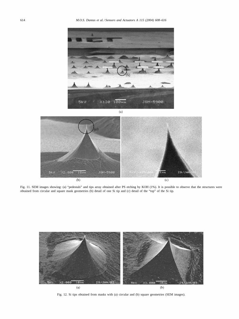
In another experiment, by increasing the anodization time(55 min) and using array of circles and rectangles mask withdifferent areas, PS was formed under all circular geometrieswith 90�m diameter and the top of the Si pedestals couldbe removed during KOH etching for 8 min. Then, some Sitips were formed, as shown inFig. 11.
Fig. 11b shows a detail of a tip with 45�m of heightobtained with circular geometry mask. The “top” of the Sitip is about 0.1�m in diameter (in detail,Fig. 11c). A thinPS layer remained on the base of the Si tip indicates thatKOH etching time should be increased in order to achievetotal PS etching.
An interesting point can be observed inFig. 12: differ-ent Si tip profiles were obtained as function of the maskgeometry. Si tip obtained from the square mask geome-try has “pyramidal” shape with four well-defined planes(Fig. 12b), while Si tip fabricated from a circular mask ge-ometry shows “conical” shape with little radial lines on thissurface (Fig. 12a). Tips obtained by square mask geometry
will not be defined in its superior extremity as a “needle”,but as a base with corners.
In Fig. 13 it is possible to see that, although the circleand rectangular geometries have the same dimensions (∅ =d = 100�m), the square “pedestal” has Si width higherthan the circular one in the region close to the “top” of the“pedestal”. These results are assigned to the different elec-tric current lines distribution and chemical reagent speciesconcentration, whose are strongly dependent on the geome-tries exposed to the electrochemical process[17].
Fig. 10. SEM photographs showing: (a) “pedestals” of monocrystalline Siafter etch of PS layer by KOH and (b) detail of one Si “pedestal”. Themeasurements shown in this image correspond to the PS layer thicknessin depth and laterally (due to isotropic PS formation).
614 M.O.S. Dantas et al. / Sensors and Actuators A 115 (2004) 608–616
Fig. 11. SEM images showing: (a) “pedestals” and tips array obtained after PS etching by KOH (1%). It is possible to observe that the structures wereobtained from circular and square mask geometries (b) detail of one Si tip and (c) detail of the “top” of the Si tip.
Fig. 12. Si tips obtained from masks with (a) circular and (b) square geometries (SEM images).

M.O.S. Dantas et al. / Sensors and Actuators A 115 (2004) 608–616 615
Fig. 13. Transversal image (SEM) of Si “pedestals” obtained from circularand square mask geometries.
4. Conclusions
Si microstructures were successfully fabricated by HI–PStechnique: the combination of PS sacrificial layers with HImask.
The results obtained show that HI with RTA maskingpresents good definition of anodization regions and makesit possible to obtain selective, thick and isotropic PS on Sisurface.
Si membranes with controlled thickness (from 1 to 4�m)were fabricated by applying additional CTA processes. How-ever, the ion implantation dose must be raised to obtain thickSi layers without defects. No visual stress was observed inthe membranes fabricated, even in the relatively large struc-tures (dimensions about 200�m × 200�m, without CTA(thickness about 1�m) [3]), but future work will be focusedin characterization of mechanical properties of the mem-branes such as the residual stress, Young modulus, hardness,and fatigue (with and without CTA process).
Applying HI–PS, an array of Si microtips was producedwith different tip shapes. Mask geometries and anodizationtime define the height and shape of the Si tips. Then, it ispossible to fabricate large quantities of Si tips in the sameprocessing with good repeatability.
This process neither bends nor damages the Si tips andmembranes, thus it is presented as a promising procedureto reduce the costs and complexity of microstructures fabri-cation, which promotes MEMS integration into microelec-tronic devices.
Acknowledgements
The authors would like to thank theLaboratório de Mi-croscopia Eletronica at LNLS, Campinas, Brazil, for theelectron microscopy work performed with the JSM-5900LVmicroscope, theLaboratório de Sistemas Integráveis at Es-cola Politécnica from Universidade de São Paulo, Brazil,
for the electron microscopy work performed with theSEM-515 microscope and for RTA process, CAPES andCNPq (476673/01–1(NV)) for financial support.
References
[1] E. Galeazzo, W.J. Salcedo, H.E.M. Peres, F.J.R. Fernandez, Poroussilicon patterned by hydrogen ion implantation, Sens. Actuators B76 (2001) 343–346.
[2] M.O.S. Dantas, E. Galeazzo, H.E.M. Peres, F.J.R. Fernandez, Siliconmicromechanical structures fabricated by electrochemical process, in:Proceedings of the First IEEE International Conference on Sensors,IEEE Sensors 2002, Orlando, USA, 2002, 575–579.
[3] M.O.S. Dantas, E. Galeazzo, H.E.M. Peres, F.J.R. Fernandez, Siliconmicromechanical structures fabricated by electrochemical process,IEEE Sens. J. 3 (6) (2003) 722–727.
[4] I. Schechter, M. Ben-Chorin, A. Kux, Gas sensing properties ofporous silicon, Anal. Chem. 67 (1995) 3727–3732.
[5] E. Galeazzo, H.E.M. Peres, G. do Santos, N. Peixoto, F.J.R. Fer-nandez, Gas sensitive porous silicon devices: responses to organicvapors, Sens. Actuators B 93 (2003) 384–390.
[6] H.F. Arrand, et al., Application of porous silicon to optical waveg-ueding technology, IEEE J. Selected Topics Quantum Electron. 4(1998) 975–982.
[7] L. Pavesi, Will silicon be the photonic material of the third mille-nium? J. Phys.: Cond. Matter 15 (2003) R1169–R1196.
[8] F. Hedrich, S. Billat, W. Lang, Structuring of membrane sensors usingsacrificial porous silicon, Sens. Actuators A 84 (2000) 315–323.
[9] R. Krüger, M. Arens-Fischer, H. Thönissen, M.G. Münder, H. Berger,S. Lüth, W. Hilbrich, Theiss, formation of porous silicon on patternedsubstrates, Thin Solid Films 276 (1996) 257–260.
[10] M. Madou, Fundamentals of Microfabrication. CRC Press, 1997, pp.145–208.
[11] H.E.M. Peres, E. Galeazzo, M.O.S. Dantas, F.J. Ramirez-Fernandez,Porous silicon masking by silicon oxide and hydrogen ion implanta-tion, in: Proceeding of the XVI International Conference on Micro-electronics and Packaging, SBmicro 2001, Pirenópilis, Goiás, Brazil,2001, pp. 118–121.
[12] W. Gopel, J. Hesse, J.N. Zemel, Sensors, VHC, 1991.[13] R.J. Grow, S.C. Minne, S.R. Manalis, C.F. Quate, Silicon nitride
cantilevers with oxidation-sharpened silicon tips for atomic forcemicroscopy, J. Microelectromech. Syst. 11 (4) (2002) 317–321.
[14] D. Kim, S.J. Kwon, J.D. Lee, Fabrication of silicon field emittersby forming porous silicon, J. Vacuum Sci. Technol. B 14 (1996)1906–1909.
[15] M.O. Heuschkel, M. Fejtl, M. Raggenbass, D. Bertrand, P. Renaud,A three-dimensional multi-electrode array for multi-site stimulationand recording in acute brain slices, J. Neurosci. Methods 114 (2002)135–148.
[16] V. Lehmann, S. Rönnebeck, The physics of macropore formation inlow doped p-type silicon, J. Electrochem. Soc. 146 (1999) 2968–2975.
[17] M. Datta, D. Landolt, Fundamental aspects and applications ofelectrochemical microfabrication, Electrochim. Acta 45 (2000)2535–2558.
Biographies
Michel Oliveira da Silva Dantas was born in São Paulo, Brazil in 1977.He received his degree in technology from Faculdade de Tecnologia deSão Paulo in 2000 and obtained his MS degree in electrical engineeringfrom Universidade de São Paulo in 2003. Presently, he is pursuing

616 M.O.S. Dantas et al. / Sensors and Actuators A 115 (2004) 608–616
his PhD degree at the Sensores Integráveis e Microssistemas group inthe Laboratório de Microeletronica of Escola Politécnica from Univer-sidade de São Paulo, Brazil. His PhD work involves the fabricationof microstructures applying the potential offered by the porous silicontechnology.
Elisabete Galeazzo obtained her degree in physics from the Universidadede São Paulo in 1989. She has been a researcher at the Laboratóriode Microeletronica of Escola Politécnica da Universidade de São Paulosince 1990, where she received a MS degree in 1993 and her PhDdegree in electrical engineering in 2000. Her current research is focusedon the development of porous silicon gas sensors and microfabricationtechnologies using porous silicon.
Henrique Estanislau Maldonado Peres received his BS degree in physicsin 1990, his MS degree in 1996 and his PhD degree in 2003, both inelectrical engineering from Universidade de São Paulo. He works atthe Sensores Integráveis e Microssistemas group in the Laboratório deMicroeletronica of Escola Politécnica from Universidade de São Paulo,Brazil. His research interest includes microelectronics processing, MEMSand sensors integration.
Francisco Javier Ramirez-Fernandez is an associate professor at theUniversidade de São Paulo, SP, Brazil. He had his degree in electricalengineering in 1970 from UTE Santiago, Chile, his MS and PhD degreesin microelectronics in 1978 and 1986 from USP, Brazil. He is Vice-Headof the Microelectronic Laboratory LME/EPUSP, Head of Integrated Sen-sors and Microsystems Division. His technological development include:bipolar low power transistor, operational amplifier, voltage regulators,integrated injection logic, high power integrated circuits technology,BIFET technology, VLSI magneto transistor, Pd-MOSFET gas sensors,porous silicon technology, electronic nose, and neuro-electronic arrays.
Abdelhamid Errachid was born in Khenifra, Morocco in 1966. Hegraduated in physics from the University M. Ismail, Meknes in 1992,and received a PhD degree in electronic engineering from UniversitatAutònoma de Barcelona, Spain in 1998. From 1992 to 2001, he workedat Centro Nacional de Microelectronica (CNM) as a PhD student anda post-doctoral researcher. At the end of 2001, he joined the CBEN atthe University of Barcelona as a researcher within the Spanish “Ramóny Cajal” Program. He worked in the development of chemical sensorsbased on ISFET and microelectrodes and on integrated instrumentationfor ISFETs. His current research activity is focused on sensing devicesfor nanobiotechnology.