high performance aerospace and defense solutions · of aerospace and defense systems including...
TRANSCRIPT

High performance aerospaceand defense solutions
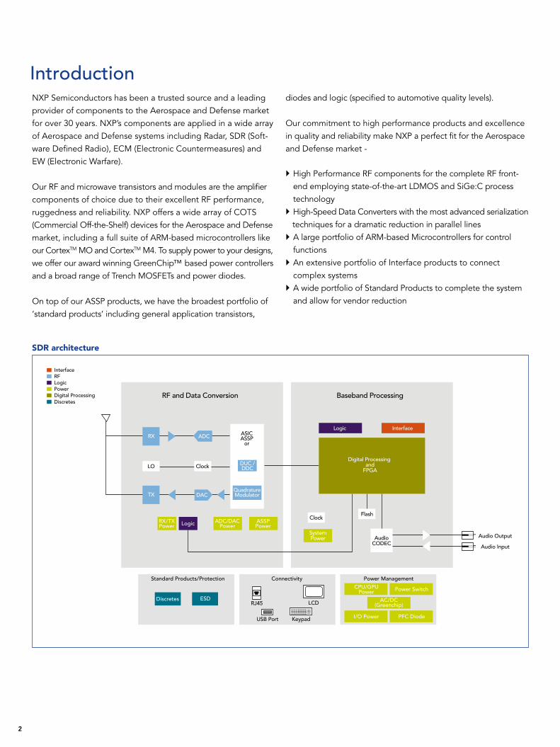
NXP Semiconductors has been a trusted source and a leading provider of components to the Aerospace and Defense market for over 30 years. NXP’s components are applied in a wide array of Aerospace and Defense systems including Radar, SDR (Soft-ware Defined Radio), ECM (Electronic Countermeasures) and EW (Electronic Warfare).
Our RF and microwave transistors and modules are the amplifier components of choice due to their excellent RF performance, ruggedness and reliability. NXP offers a wide array of COTS (Commercial Off-the-Shelf) devices for the Aerospace and Defense market, including a full suite of ARM-based microcontrollers like our CortexTM MO and CortexTM M4. To supply power to your designs, we offer our award winning GreenChip™ based power controllers and a broad range of Trench MOSFETs and power diodes.
On top of our ASSP products, we have the broadest portfolio of ‘standard products’ including general application transistors,
diodes and logic (specified to automotive quality levels).
Our commitment to high performance products and excellence in quality and reliability make NXP a perfect fit for the Aerospace and Defense market -
} High Performance RF components for the complete RF front- end employing state-of-the-art LDMOS and SiGe:C process technology} High-Speed Data Converters with the most advanced serialization
techniques for a dramatic reduction in parallel lines} A large portfolio of ARM-based Microcontrollers for control functions} An extensive portfolio of Interface products to connect complex systems} A wide portfolio of Standard Products to complete the system and allow for vendor reduction
Introduction
ConnectivityStandard Products/Protection
Power Switch
PFC Diode
CPU/GPUPower
AC/DC(Greenchip)
I/O Power
Power Management
RX
TX
LO
QuadratureModulator
RF and Data Conversion Baseband Processing
ADC
DAC
Audio Output
Audio Input
ADC/DACPower
ASSPPower
RX/TXPower Logic
SystemPower Audio
CODEC
InterfaceLogic
Flash
InterfaceRFLogicPowerDigital Processing
Clock
ASICASSP
or
DUC /DDCClock
Digital Processing and
FPGA
LCD
KeypadUSB Port
RJ45Discretes ESD
Discretes
SDR architecture
2
ConnectivityStandard Products/Protection
Power Switch
PFC Diode
CPU/GPUPower
AC/DC(Greenchip)
I/O Power
Power Management
RX
TX
LO
QuadratureModulator
RF and Data Conversion Baseband Processing
ADC
DAC
Audio Output
Audio Input
ADC/DACPower
ASSPPower
RX/TXPower Logic
SystemPower Audio
CODEC
InterfaceLogic
Flash
InterfaceRFLogicPowerDigital Processing
Clock
ASICASSP
or
DUC /DDCClock
Digital Processing and
FPGA
LCD
KeypadUSB Port
RJ45Discretes ESD
Discretes
3
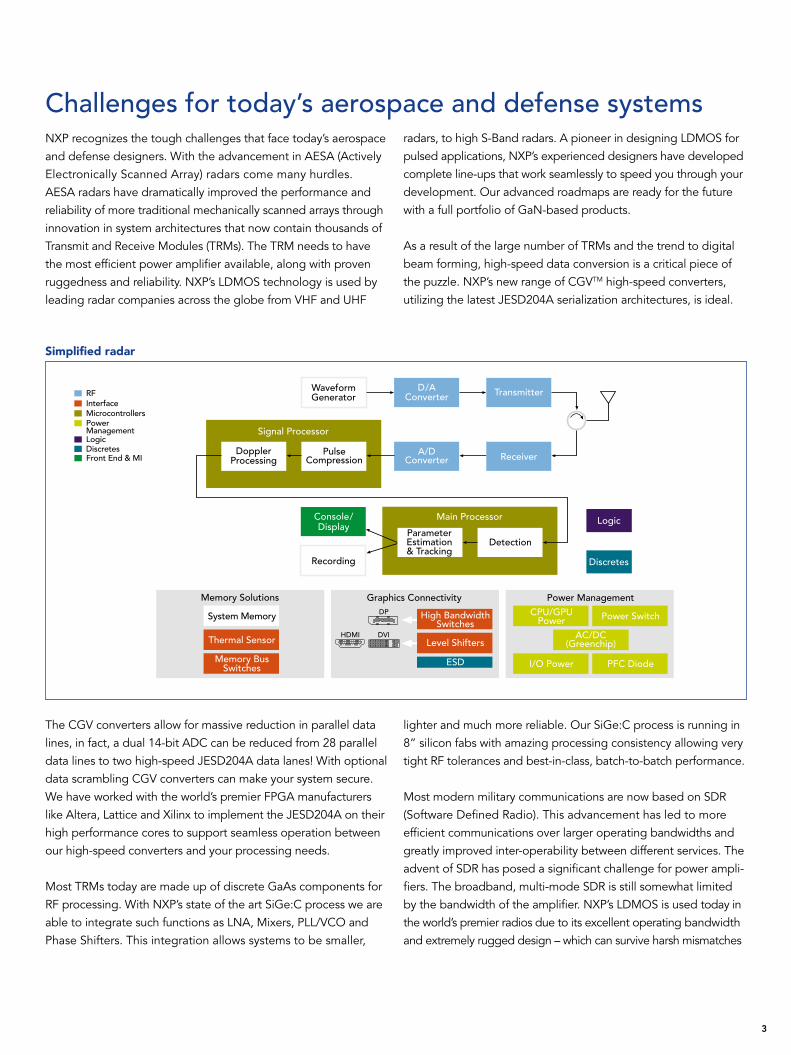
NXP recognizes the tough challenges that face today’s aerospace and defense designers. With the advancement in AESA (Actively Electronically Scanned Array) radars come many hurdles. AESA radars have dramatically improved the performance and reliability of more traditional mechanically scanned arrays through innovation in system architectures that now contain thousands of Transmit and Receive Modules (TRMs). The TRM needs to have the most efficient power amplifier available, along with proven ruggedness and reliability. NXP’s LDMOS technology is used by leading radar companies across the globe from VHF and UHF
radars, to high S-Band radars. A pioneer in designing LDMOS for pulsed applications, NXP’s experienced designers have developed complete line-ups that work seamlessly to speed you through your development. Our advanced roadmaps are ready for the future with a full portfolio of GaN-based products.
As a result of the large number of TRMs and the trend to digital beam forming, high-speed data conversion is a critical piece of the puzzle. NXP’s new range of CGVTM high-speed converters, utilizing the latest JESD204A serialization architectures, is ideal.
Challenges for today’s aerospace and defense systems
The CGV converters allow for massive reduction in parallel data lines, in fact, a dual 14-bit ADC can be reduced from 28 parallel data lines to two high-speed JESD204A data lanes! With optional data scrambling CGV converters can make your system secure. We have worked with the world’s premier FPGA manufacturers like Altera, Lattice and Xilinx to implement the JESD204A on their high performance cores to support seamless operation between our high-speed converters and your processing needs.
Most TRMs today are made up of discrete GaAs components for RF processing. With NXP’s state of the art SiGe:C process we are able to integrate such functions as LNA, Mixers, PLL/VCO and Phase Shifters. This integration allows systems to be smaller,
lighter and much more reliable. Our SiGe:C process is running in 8” silicon fabs with amazing processing consistency allowing very tight RF tolerances and best-in-class, batch-to-batch performance.
Most modern military communications are now based on SDR (Software Defined Radio). This advancement has led to more efficient communications over larger operating bandwidths and greatly improved inter-operability between different services. The advent of SDR has posed a significant challenge for power ampli-fiers. The broadband, multi-mode SDR is still somewhat limited by the bandwidth of the amplifier. NXP’s LDMOS is used today in the world’s premier radios due to its excellent operating bandwidth and extremely rugged design – which can survive harsh mismatches
Simplified radar
Logic
Discretes
ESD
Signal Processor
Graphics ConnectivityDP
DVIHDMI
System Memory
Memory Solutions
Power Switch
PFC Diode
CPU/GPUPower
AC/DC(Greenchip)
I/O Power
Power Management
PulseCompression
WaveformGenerator
D/AConverter Transmitter
A/DConverter
Console/Display
DopplerProcessing
Main Processor
Detection
Recording
Receiver
ParameterEstimation& Tracking
Thermal Sensor
Memory BusSwitches
RFInterface
Power Management
DiscretesLogic
Microcontrollers
Front End & MI
High BandwidthSwitches
Level Shifters
4
Logic
DiscretesESD
Graphics ConnectivityDP
DVIHDMI
Power Switch
PFC Diode
CPU/GPUPower
AC/DC(Greenchip)
I/O Power
Power Management
WaveformGenerator
DataConversion
TransmitFrontEnd
TimingReference
ReceiveFrontEnd
OperationalControl
RFSequencer
DigitalUp conversion
WidebandDigital
Down conversion
Console/Display
SignalProcessing
RFInterface
Power Management
DiscretesLogic
Microcontrollers
Front End & MI
High BandwidthSwitches
Level Shifters
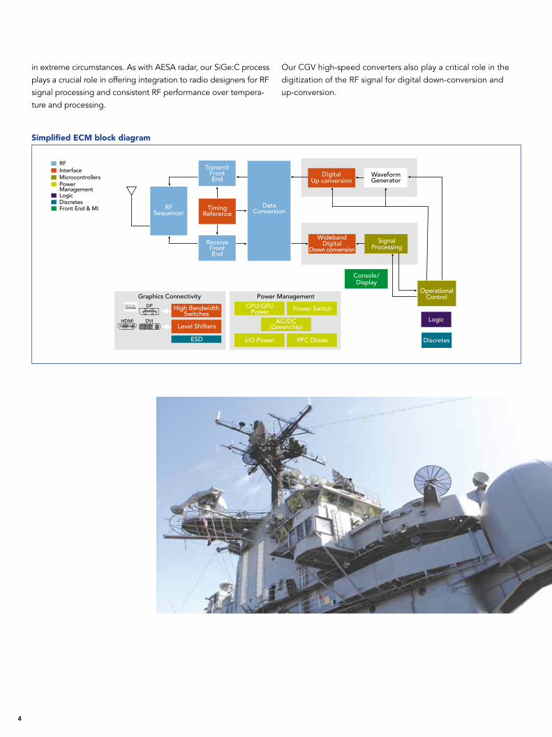
Simplified ECM block diagram
in extreme circumstances. As with AESA radar, our SiGe:C process plays a crucial role in offering integration to radio designers for RF signal processing and consistent RF performance over tempera-ture and processing.
Our CGV high-speed converters also play a critical role in the digitization of the RF signal for digital down-conversion and up-conversion.
5
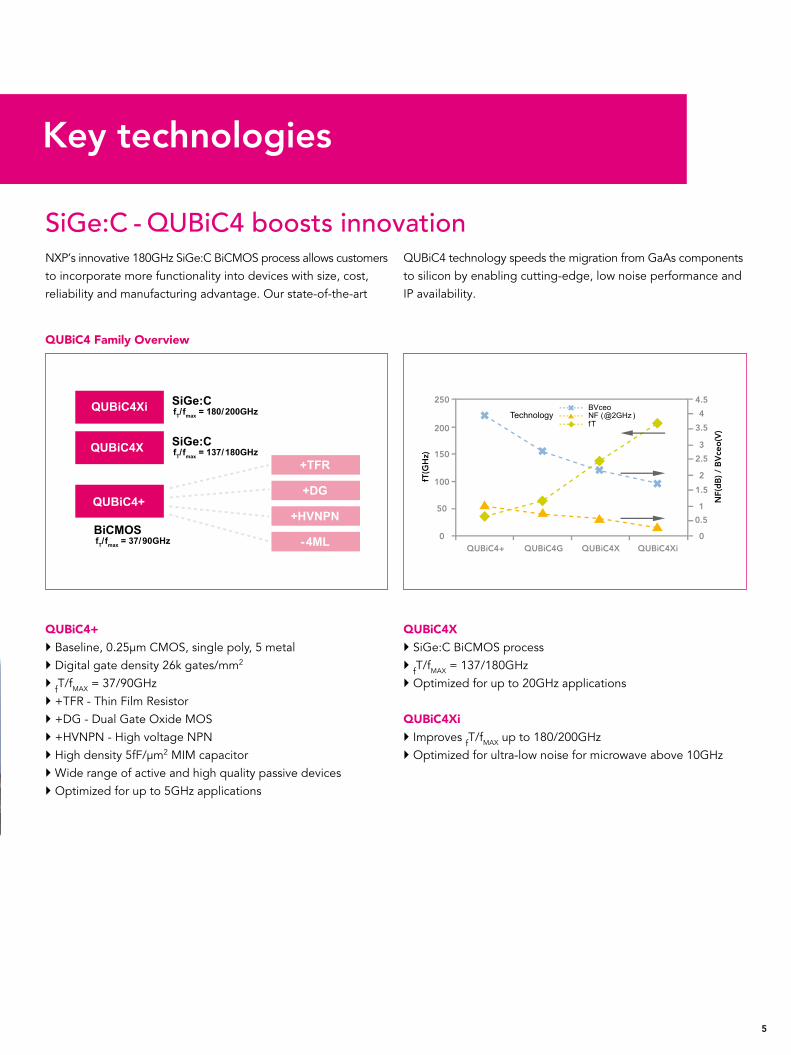
NXP’s innovative 180GHz SiGe:C BiCMOS process allows customers to incorporate more functionality into devices with size, cost, reliability and manufacturing advantage. Our state-of-the-art
QUBiC4 technology speeds the migration from GaAs components to silicon by enabling cutting-edge, low noise performance and IP availability.
QUBiC4 Family Overview
SiGe:C - QUBiC4 boosts innovation
Key technologies
QUBiC4+} Baseline, 0.25μm CMOS, single poly, 5 metal} Digital gate density 26k gates/mm2
} fT/fMAX = 37/90GHz} +TFR - Thin Film Resistor} +DG - Dual Gate Oxide MOS} +HVNPN - High voltage NPN} High density 5fF/μm2 MIM capacitor} Wide range of active and high quality passive devices} Optimized for up to 5GHz applications
QUBiC4X} SiGe:C BiCMOS process} fT/fMAX = 137/180GHz} Optimized for up to 20GHz applications
QUBiC4Xi} Improves fT/fMAX up to 180/200GHz} Optimized for ultra-low noise for microwave above 10GHz
6
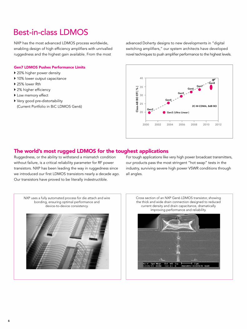
NXP has the most advanced LDMOS process worldwide, enabling design of high efficiency amplifiers with unrivalled ruggedness and the highest gain available. From the most
advanced Doherty designs to new developments in “digital switching amplifiers,” our system architects have developed novel techniques to push amplifier performance to the highest levels.
Best-in-class LDMOS
Ruggedness, or the ability to withstand a mismatch condition without failure, is a critical reliability parameter for RF power transistors. NXP has been leading the way in ruggedness since we introduced our first LDMOS transistors nearly a decade ago. Our transistors have proved to be literally indestructible.
For tough applications like very high power broadcast transmitters, our products pass the most stringent “hot swap” tests in the industry, surviving severe high power VSWR conditions through all angles.
The world’s most rugged LDMOS for the toughest applications
Gen7 LDMOS Pushes Performance Limits} 20% higher power density} 10% lower output capacitance} 25% lower Rth} 2% higher efficiency} Low memory effect} Very good pre-distortability
(Current Portfolio in BiC LDMOS Gen6)
Cross section of an NXP Gen6 LDMOS transistor, showing the thick and wide drain connection designed to reduced
current density and drain capacitance, dramatically improving performance and reliability.
NXP uses a fully automated process for die attach and wire bonding, ensuring optimal performance and
device-to-device consistency.
NXP is not only designing next-generation transistors in GaN technology with breakthrough specifications, we’re leading the charge in discovery and innovation in the field of digital transmit-ter switching power amplifiers based on GaN technology. GaN technology is truly enabling an age of universal transmitters.
7
High performance RF products
NXP’s ongoing commitment to the Aerospace and Defense market is built on a 30+ year track record of providing world class products into avionics, communications, jammer, and radar applications. For these and other high power, high performance applications, we offer state-of-the-art 28V and 50V LDMOS (Laterally Diffused Metal Oxide Semiconductor) products delivering high power density and high efficiency from a few MHz up through S-band. Our latest 7th Generation LDMOS technology offers even greater advantages over bipolar technologies, including higher gain, lower thermal impedance, improved MTTF, unparalleled thermal stability, and inherently stable pulsed performance. As the first semiconductor company to supply LDMOS-based S-band transistors with a range of 2700-3500MHz, we are expanding our product portfolio with new, higher power and higher bandwidth components based on GaN technology.
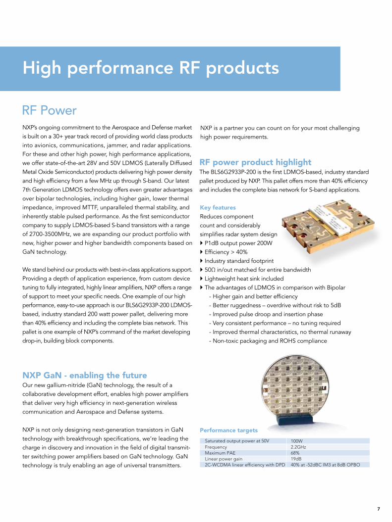
We stand behind our products with best-in-class applications support. Providing a depth of application experience, from custom device tuning to fully integrated, highly linear amplifiers, NXP offers a range of support to meet your specific needs. One example of our high performance, easy-to-use approach is our BLS6G2933P-200 LDMOS- based, industry standard 200 watt power pallet, delivering more than 40% efficiency and including the complete bias network. This pallet is one example of NXP’s command of the market developing drop-in, building block components.
RF power product highlightThe BLS6G2933P-200 is the first LDMOS-based, industry standard pallet produced by NXP. This pallet offers more than 40% efficiency and includes the complete bias network for S-band applications.
NXP GaN - enabling the futureOur new gallium-nitride (GaN) technology, the result of a collaborative development effort, enables high power amplifiers that deliver very high efficiency in next-generation wireless communication and Aerospace and Defense systems.
RF PowerNXP is a partner you can count on for your most challenging high power requirements.
Key featuresReduces component count and considerably simplifies radar system design} P1dB output power 200W} Efficiency > 40%} Industry standard footprint} 50Ω in/out matched for entire bandwidth} Lightweight heat sink included} The advantages of LDMOS in comparison with Bipolar - Higher gain and better efficiency - Better ruggedness – overdrive without risk to 5dB - Improved pulse droop and insertion phase - Very consistent performance – no tuning required - Improved thermal characteristics, no thermal runaway - Non-toxic packaging and ROHS compliance
Performance targets
2.2GHz68%19dB40% at -52dBC IM3 at 8dB OPBO
100WFrequencyMaximum PAELinear power gain2C-WCDMA linear ef�ciency with DPD
Saturated output power at 50V
8
�nal BLA0912-250R SOT502A2 960 - 1215 250 50 13.5 36 PULSED RF; class AB�nal BLA6H0912-500 SOT539A 960 - 1215 450 50 17 50 PULSED RF; class AB�nal BLA6H1011-600 SOT539A 1030 - 1090 600 52 19 50 PULSED RF; class AB�nal BLA6G1011-200R SOT502A2 1030 - 1090 200 65 20 28 PULSED RF; class AB
Function Type Packagefrange PL (av) ηD Gp @VDS
Mode of operationMHz W % dB V
driver BLL6H0514-25 SOT467C 500 - 1400 25 (min) 50 19 50 PULSED RF; class ABnal BLL6H1214-500 SOT539A 1200 - 1400 500 (min) 50 17 50 PULSED RF; class ABnal BLL6H1214L(S)-250 SOT502 1200 - 1400 250 55 17 50 Pulsed RFnal BLL6HL(S)0514-130 SOT1135 1200 - 1400 130 50 18 50 Pulsed RF
Function Type Packagefrange PL (av) ηD Gp @VDS
Mode of operationMHz W % dB V
driver BLS6G2731-6G SOT975C 2700 - 3100 6 33 15 32 PULSED RF; class ABdriver BLS6G3135-20 SOT608A 3100 - 3500 20 45 15.5 32 PULSED RF; class ABdriver BLS6G3135S-20 SOT608B 3100 - 3500 20 45 15.5 32 PULSED RF; class AB nal BLS6G2731-120 SOT502A 2700 - 3100 120 48 13.5 32 PULSED RF; class AB nal BLS6G2731S-120 SOT502B 2700 - 3100 120 48 13.5 32 PULSED RF; class AB nal BLS6G2933S-130 SOT922-1 2900 - 3300 130 47 12.5 32 PULSED RF; class AB nal BLS6G3135-120 SOT502A 3100 - 3500 120 43 11 32 PULSED RF; class AB nal BLS6G3135S-120 SOT502B 3100 - 3500 120 43 11 32 PULSED RF; class AB nal BLS6G2933P-200 pallet 2900 - 3300 200 45 11 32 PULSED RF; class AB nal BLS6G2731P-200 pallet 2700 - 3100 200 45 11 32 PULSED RF; class AB nal BLS6G2731S-130 SOT922 2700 - 3100 130 49 13 32 Pulsed RF
L-Band LDMOS transistors
S-Band LDMOS transistors
Function Type Packagefrange PL (av) ηD Gp @VDS
Mode of operationMHz W % dB V
driver BLL6H0514-25 SOT467C 500 - 1400 25 (min) 50 19 50 PULSED RF; class AB
Avionics LDMOS transistors
Function Type Packagefrange PL(AV) ηD Gp @VDS
Mode of operationMHz W % dB V
driver
BLF871 SOT467C0 - 1000 100 47 21 40 2-TONE0 - 1000 24 33 22 40 DVB-T
driver BLF871S SOT467B0 - 1000 100 47 21 40 2-TONE0 - 1000 24 33 22 40 DVB-T
driver BLF881 SOT467C0 - 1000 140 49 21 50 2-TONE0 - 1000 33 34 21 50 DVB-T
driver BLF881S SOT467C0 - 1000 140 49 21 50 2-TONE0 - 1000 33 34 21 50 DVB-T
�nal BLF645 SOT540A0 - 1400 100 45 18 32 2-TONE0 - 1400 100 56 18 32 CW
driver BLF571 SOT467C 0 - 1000 20 70 27.5 50 CW�nal BLF573 SOT502A3 0 - 1000 300 70 27.2 50 CW�nal BLF573S SOT502B 0 - 1000 300 70 27.2 50 CW�nal BLF574 SOT539A 0 - 1000 500 70 26.5 50 CW
�nal BLF578 SOT539A0 - 1000 1200 71 24 50 PULSED RF0 - 1000 1000 75 26 50 CW
Function Type Packagefrange PL(AV) ηD Gp @VDS
Mode of operationMHz W % dB V
driver BLF871 SOT467C0 - 1000 100 47 21 40 2-TONE0 - 1000 24 33 22 40 DVB-T
driver BLF871S SOT467B0 - 1000 100 47 21 40 2-TONE0 - 1000 24 33 22 40 DVB-T
�nal BLF878 SOT979A470 - 860 300 32 21 42 CW470 - 860 75 46 21 42 DVB-T
driver BLF881S SOT467C0 - 1000 120 48 21 50 2-TONE0 - 1000 30 31 21 50 DVB-T
driver BLF881 SOT467C0 - 1000 120 48 21 50 2-TONE0 - 1000 30 31 21 50 DVB-T
�nal BLF888 SOT979A470 - 860 250 46 19 50 2-TONE470 - 860 110 31 19 50 DVB-T
�nal BLF888AS SOT539B470 - 860 250 46 19 50 2-TONE470 - 860 110 31 19 50 DVB-T
�nal BLF888A SOT539B470 - 860 255 47 19 50 2-TONE470 - 860 115 32 19 50 DVB-T
0 -1000MHz (UHF/VHF/HF/ISM) LDMOS line up
470-876MHz (UHF) LDMOS line up
�nal BLA0912-250R SOT502A2 960 - 1215 250 50 13.5 36 PULSED RF; class AB�nal BLA6H0912-500 SOT539A 960 - 1215 450 50 17 50 PULSED RF; class AB�nal BLA6H1011-600 SOT539A 1030 - 1090 600 52 19 50 PULSED RF; class AB�nal BLA6G1011-200R SOT502A2 1030 - 1090 200 65 20 28 PULSED RF; class AB
Function Type Packagefrange PL (av) ηD Gp @VDS
Mode of operationMHz W % dB V
driver BLL6H0514-25 SOT467C 500 - 1400 25 (min) 50 19 50 PULSED RF; class ABnal BLL6H1214-500 SOT539A 1200 - 1400 500 (min) 50 17 50 PULSED RF; class ABnal BLL6H1214L(S)-250 SOT502 1200 - 1400 250 55 17 50 Pulsed RFnal BLL6HL(S)0514-130 SOT1135 1200 - 1400 130 50 18 50 Pulsed RF
Function Type Packagefrange PL (av) ηD Gp @VDS
Mode of operationMHz W % dB V
driver BLS6G2731-6G SOT975C 2700 - 3100 6 33 15 32 PULSED RF; class ABdriver BLS6G3135-20 SOT608A 3100 - 3500 20 45 15.5 32 PULSED RF; class ABdriver BLS6G3135S-20 SOT608B 3100 - 3500 20 45 15.5 32 PULSED RF; class AB nal BLS6G2731-120 SOT502A 2700 - 3100 120 48 13.5 32 PULSED RF; class AB nal BLS6G2731S-120 SOT502B 2700 - 3100 120 48 13.5 32 PULSED RF; class AB nal BLS6G2933S-130 SOT922-1 2900 - 3300 130 47 12.5 32 PULSED RF; class AB nal BLS6G3135-120 SOT502A 3100 - 3500 120 43 11 32 PULSED RF; class AB nal BLS6G3135S-120 SOT502B 3100 - 3500 120 43 11 32 PULSED RF; class AB nal BLS6G2933P-200 pallet 2900 - 3300 200 45 11 32 PULSED RF; class AB nal BLS6G2731P-200 pallet 2700 - 3100 200 45 11 32 PULSED RF; class AB nal BLS6G2731S-130 SOT922 2700 - 3100 130 49 13 32 Pulsed RF
L-Band LDMOS transistors
S-Band LDMOS transistors
Function Type Packagefrange PL (av) ηD Gp @VDS
Mode of operationMHz W % dB V
driver BLL6H0514-25 SOT467C 500 - 1400 25 (min) 50 19 50 PULSED RF; class AB
Avionics LDMOS transistors
9
Function Type Packagefrange PL(AV) ηD Gp @VDS
Mode of operationMHz W % dB V
driver
BLF871 SOT467C0 - 1000 100 47 21 40 2-TONE0 - 1000 24 33 22 40 DVB-T
driver BLF871S SOT467B0 - 1000 100 47 21 40 2-TONE0 - 1000 24 33 22 40 DVB-T
driver BLF881 SOT467C0 - 1000 140 49 21 50 2-TONE0 - 1000 33 34 21 50 DVB-T
driver BLF881S SOT467C0 - 1000 140 49 21 50 2-TONE0 - 1000 33 34 21 50 DVB-T
�nal BLF645 SOT540A0 - 1400 100 45 18 32 2-TONE0 - 1400 100 56 18 32 CW
driver BLF571 SOT467C 0 - 1000 20 70 27.5 50 CW�nal BLF573 SOT502A3 0 - 1000 300 70 27.2 50 CW�nal BLF573S SOT502B 0 - 1000 300 70 27.2 50 CW�nal BLF574 SOT539A 0 - 1000 500 70 26.5 50 CW
�nal BLF578 SOT539A0 - 1000 1200 71 24 50 PULSED RF0 - 1000 1000 75 26 50 CW
Function Type Packagefrange PL(AV) ηD Gp @VDS
Mode of operationMHz W % dB V
driver BLF871 SOT467C0 - 1000 100 47 21 40 2-TONE0 - 1000 24 33 22 40 DVB-T
driver BLF871S SOT467B0 - 1000 100 47 21 40 2-TONE0 - 1000 24 33 22 40 DVB-T
�nal BLF878 SOT979A470 - 860 300 32 21 42 CW470 - 860 75 46 21 42 DVB-T
driver BLF881S SOT467C0 - 1000 120 48 21 50 2-TONE0 - 1000 30 31 21 50 DVB-T
driver BLF881 SOT467C0 - 1000 120 48 21 50 2-TONE0 - 1000 30 31 21 50 DVB-T
�nal BLF888 SOT979A470 - 860 250 46 19 50 2-TONE470 - 860 110 31 19 50 DVB-T
�nal BLF888AS SOT539B470 - 860 250 46 19 50 2-TONE470 - 860 110 31 19 50 DVB-T
�nal BLF888A SOT539B470 - 860 255 47 19 50 2-TONE470 - 860 115 32 19 50 DVB-T
0 -1000MHz (UHF/VHF/HF/ISM) LDMOS line up
470-876MHz (UHF) LDMOS line up
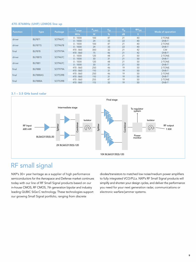
3.1 – 3.5 GHz band radar
Intermediate stage
10X BLS6G3135(S)-120
Split
ter
Final stage
To regulator system
RF Input600 mW
BLS6G3135(S)-20 Powermonitor
IsolatorIsolator
RF outputC
ombi
ner
1 KW
2X BLS6G3135(S)-120
Split
ter
Com
bine
r
NXP’s 30+ year heritage as a supplier of high performance semiconductors for the Aerospace and Defense market continues today with our line of RF Small Signal products based on our in-house CMOS, RF CMOS, 7th generation bipolar and industry leading QUBIC SiGe:C technology. These technologies support our growing Small Signal portfolio, ranging from discrete
diodes/transistors to matched low noise/medium power amplifiers to fully integrated VCO/PLLs. NXP’s RF Small Signal products will simplify and shorten your design cycles, and deliver the performance you need for your next generation radar, communications or electronic warfare/jammer systems.
RF small signal
10
NXP’s QUBiCxi process delivers an impressive noise figure of 0.5dB at 13GHz – performance at one time the exclusive domain of GaAs HEMT devices. With the inherent integration
capability of silicon, such as built-in power-down functionality, NXP enables best-in-class performance and ease-of-use for your receive chain amplifier needs.
MMIC low noise amplifiers
MMIC medium power amplifiersLow noise LO generators for VSAT applications
Type Package
fIN(REF) VCC ICC PLL phase noise @ N=64, @100kHz
PLL Output buffer Input
fo(RF) Po RLout(RF) Si
Typ Typ Max Typ Max Min
MHz V mA dBc/Hz GHz dBm dB dBm
TFF1003HN SOT616 50~815 3.3 100 -92 12.8~13.05 -5 -10 -10
TFF1007HN* SOT616 230.46~234.38 3.3 100 -104 14.75~15 -3 -10 -10
Low noise LO generators for general microwave applications
Type PackagefIN(REF)
VCC ICCPLL phase noise @
N=64PLL Output buffer Input
fo(RF) Po RLout(RF) STyp Typ @ 100kHz @ 10MHz Min Typ Max Typ Max Min
MHz V mA dBc/Hz dBc/Hz GHz GHz GHz dBm dB dBmTFF11070HN* SOT616 27 - 448 3.3 100 -95 -131 6.84 7.00 7.16 -5 -10 -10TFF11073HN* SOT616 28 - 468 3.3 100 -95 -131 7.16 7.33 7.49 -5 -10 -10TFF11077HN* SOT616 29 - 490 3.3 100 -95 -131 7.49 7.67 7.84 -5 -10 -10TFF11080HN* SOT616 31 - 513 3.3 100 -95 -131 7.84 8.02 8.21 -5 -10 -10TFF11084HN* SOT616 32 - 537 3.3 100 -95 -131 8.21 8.40 8.59 -5 -10 -10TFF11088HN* SOT616 34 - 562 3.3 100 -95 -131 8.59 8.79 8.99 -5 -10 -10TFF11092HN* SOT616 35 - 588 3.3 100 -95 -131 8.99 9.20 9.41 -5 -10 -10TFF11096HN* SOT616 37 - 616 3.3 100 -95 -131 9.41 9.63 9.85 -5 -10 -10TFF11101HN* SOT616 38 - 644 3.3 100 -95 -131 9.85 10.07 10.31 -5 -10 -10TFF11105HN* SOT616 40 - 674 3.3 100 -95 -131 10.31 10.54 10.79 -5 -10 -10TFF11110HN* SOT616 42 - 706 3.3 100 -95 -131 10.79 11.03 11.29 -5 -10 -10TFF11115HN* SOT616 44 - 738 3.3 100 -95 -131 11.29 11.55 11.81 -5 -10 -10TFF11121HN* SOT616 46 - 773 3.3 100 -95 -131 11.81 12.09 12.36 -5 -10 -10TFF11126HN* SOT616 48 - 809 3.3 100 -95 -131 12.36 12.65 12.94 -5 -10 -10TFF11139HN* SOT616 53 - 886 3.3 100 -95 -131 13.54 13.85 14.17 -5 -10 -10TFF11145HN* SOT616 55 - 927 3.3 100 -95 -131 14.17 14.50 14.83 -5 -10 -10TFF11152HN* SOT616 58 - 970 3.3 100 -95 -131 14.83 15.18 15.52 -5 -10 -10
* = check product status, as this type has not been released for mass productionBold Red = New, highly recommended product
* = check product status, as this type has not been released for mass productionBold Red = New, highly recommended product
SiGe:C MMIC LNAs
Type Package Vsupply (Typ) C L(1dB)
(V)
IRL
(dB)
IRL
(dB)
OIP3 (Typ)
(dBm)
P (Typ)
(dBmW)
NF (Typ)
(dB)
Gass (Typ)
(dB)
@ f =
(MHz)
@ I =
(mA)BGU7051* SOT650BGU7052* SOT650BGU7053* SOT650BGU7054* SOT650
* = check product status, as this type has not been released for mass productionBold Red = New, highly recommended product
3.3 65 900 20.9 0.7 17.8 34 22 15.8
3.3 65 3500 20 1.1 18 35 20 153.3 65 2500 20 1 18 35 20 153.3 65 1900 20.1 0.9 18 35.5 20 15
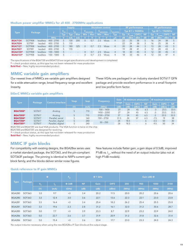
Medium power ampli�er MMICs for all 400 - 2700MHz applications
Supply Shutdown control RF performance RF performance
Type Package fVcc Icc VI(D)L(SHDN) VI(D)H(SHDN) II(D)L(SHDN) Typ @ f = 940MHz Typ @ f = 1960MHz
Typ Typ Max Min Max Min Max Typ Gp PL(1dB) OIP3 NF Gp PL(1dB) OIP3 NF MHz V mA mA V V V V µA dB dBm dBm dB dB dBm dBm dB
BGA7124 SOT908 leadless 400 - 2700 5 130 200 0 0.7 2.5 Vbias 4 22 25 38 5 16 24 38 5BGA7024 SOT89 leaded 400 - 2700 5 110 - - - - - - 22 24 38 3 16 25 38 4BGA7127 SOT908 leadless 400 - 2700 5 180 325 0 0.7 2.5 Vbias 4 20 28 44 3 13 28 43 5BGA7027 SOT89 leaded 400 - 2700 5 170 - - - - - - 19 28 41 3 12 28 43 4BGA6130* SOT908 leadless 100 - 1000 5 - - 0 0.7 2.5 Vbias 4 18 30 45 4 12 30 45 4BGA6133* SOT908 leadless 100 - 1000 5 - - 0 0.7 2.5 Vbias 4 18 33 46 4 12 33 47 4
SiGe:C MMICs (for e.g. GPS)
Type Package
Supply voltage
Supply current
@ 1.575 GHz
Insertion power gain
Noise �gure
Input power at 1 dB gain compression
Input third-order intercept pointf1 = 1713 MHz, f2 = 1851 MHz
Vcc Icc |s21 |2 NF PI(1 dB) IP3i
V mA dB dB dBm dBm
Min Max Min Type Max Min Type Max TypeVcc = 1.8V, Min
Vcc = 1.8V, Type
Vcc = 2.5V, Icc =5mA
Vcc = 2.85V, Min
Vcc = 2.85V, Type
Vcc = 1.8V, Min
Vcc = 1.8V, Type
Vcc = 2.5V, Icc =
5 mA Min
Vcc = 2.85V,
Vcc = 2.85V,
Type
i
BGU7003 SOT891 2.2 2.85 3 - 15 16 18,3 20 0.8 - - -20 - - - - 0 - -BGU7005 SOT886 1.5 2.85 - 4.5 - - 16.5 - 0.9 -14 -11 - -11 -8 5 9 - 5 12BGU7007 SOT886 1.5 2.85 - 4.8 - - 18 - 0.9 -14 -11 - -11 -8 5 9 - 5 12
Low noise LO generators for VSAT applications
Type Package
fIN(REF) VCC ICC PLL phase noise @ N=64, @100kHz
PLL Output buffer Input
fo(RF) Po RLout(RF) Si
Typ Typ Max Typ Max Min
MHz V mA dBc/Hz GHz dBm dB dBm
TFF1003HN SOT616 50~815 3.3 100 -92 12.8~13.05 -5 -10 -10
TFF1007HN* SOT616 230.46~234.38 3.3 100 -104 14.75~15 -3 -10 -10
Low noise LO generators for general microwave applications
Type PackagefIN(REF)
VCC ICCPLL phase noise @
N=64PLL Output buffer Input
fo(RF) Po RLout(RF) STyp Typ @ 100kHz @ 10MHz Min Typ Max Typ Max Min
MHz V mA dBc/Hz dBc/Hz GHz GHz GHz dBm dB dBmTFF11070HN* SOT616 27 - 448 3.3 100 -95 -131 6.84 7.00 7.16 -5 -10 -10TFF11073HN* SOT616 28 - 468 3.3 100 -95 -131 7.16 7.33 7.49 -5 -10 -10TFF11077HN* SOT616 29 - 490 3.3 100 -95 -131 7.49 7.67 7.84 -5 -10 -10TFF11080HN* SOT616 31 - 513 3.3 100 -95 -131 7.84 8.02 8.21 -5 -10 -10TFF11084HN* SOT616 32 - 537 3.3 100 -95 -131 8.21 8.40 8.59 -5 -10 -10TFF11088HN* SOT616 34 - 562 3.3 100 -95 -131 8.59 8.79 8.99 -5 -10 -10TFF11092HN* SOT616 35 - 588 3.3 100 -95 -131 8.99 9.20 9.41 -5 -10 -10TFF11096HN* SOT616 37 - 616 3.3 100 -95 -131 9.41 9.63 9.85 -5 -10 -10TFF11101HN* SOT616 38 - 644 3.3 100 -95 -131 9.85 10.07 10.31 -5 -10 -10TFF11105HN* SOT616 40 - 674 3.3 100 -95 -131 10.31 10.54 10.79 -5 -10 -10TFF11110HN* SOT616 42 - 706 3.3 100 -95 -131 10.79 11.03 11.29 -5 -10 -10TFF11115HN* SOT616 44 - 738 3.3 100 -95 -131 11.29 11.55 11.81 -5 -10 -10TFF11121HN* SOT616 46 - 773 3.3 100 -95 -131 11.81 12.09 12.36 -5 -10 -10TFF11126HN* SOT616 48 - 809 3.3 100 -95 -131 12.36 12.65 12.94 -5 -10 -10TFF11139HN* SOT616 53 - 886 3.3 100 -95 -131 13.54 13.85 14.17 -5 -10 -10TFF11145HN* SOT616 55 - 927 3.3 100 -95 -131 14.17 14.50 14.83 -5 -10 -10TFF11152HN* SOT616 58 - 970 3.3 100 -95 -131 14.83 15.18 15.52 -5 -10 -10
* = check product status, as this type has not been released for mass productionBold Red = New, highly recommended product
* = check product status, as this type has not been released for mass productionBold Red = New, highly recommended product
SiGe:C MMIC LNAs
Type Package Vsupply (Typ) C L(1dB)
(V)
IRL
(dB)
IRL
(dB)
OIP3 (Typ)
(dBm)
P (Typ)
(dBmW)
NF (Typ)
(dB)
Gass (Typ)
(dB)
@ f =
(MHz)
@ I =
(mA)BGU7051* SOT650BGU7052* SOT650BGU7053* SOT650BGU7054* SOT650
* = check product status, as this type has not been released for mass productionBold Red = New, highly recommended product
3.3 65 900 20.9 0.7 17.8 34 22 15.8
3.3 65 3500 20 1.1 18 35 20 153.3 65 2500 20 1 18 35 20 153.3 65 1900 20.1 0.9 18 35.5 20 15
Medium power ampli�er MMICs for all 400 - 2700MHz applications
Supply Shutdown control RF performance RF performance
Type Package fVcc Icc VI(D)L(SHDN) VI(D)H(SHDN) II(D)L(SHDN) Typ @ f = 940MHz Typ @ f = 1960MHz
Typ Typ Max Min Max Min Max Typ Gp PL(1dB) OIP3 NF Gp PL(1dB) OIP3 NF MHz V mA mA V V V V µA dB dBm dBm dB dB dBm dBm dB
BGA7124 SOT908 leadless 400 - 2700 5 130 200 0 0.7 2.5 Vbias 4 22 25 38 5 16 24 38 5BGA7024 SOT89 leaded 400 - 2700 5 110 - - - - - - 22 24 38 3 16 25 38 4BGA7127 SOT908 leadless 400 - 2700 5 180 325 0 0.7 2.5 Vbias 4 20 28 44 3 13 28 43 5BGA7027 SOT89 leaded 400 - 2700 5 170 - - - - - - 19 28 41 3 12 28 43 4BGA6130* SOT908 leadless 100 - 1000 5 - - 0 0.7 2.5 Vbias 4 18 30 45 4 12 30 45 4BGA6133* SOT908 leadless 100 - 1000 5 - - 0 0.7 2.5 Vbias 4 18 33 46 4 12 33 47 4
SiGe:C MMICs (for e.g. GPS)
Type Package
Supply voltage
Supply current
@ 1.575 GHz
Insertion power gain
Noise �gure
Input power at 1 dB gain compression
Input third-order intercept pointf1 = 1713 MHz, f2 = 1851 MHz
Vcc Icc |s21 |2 NF PI(1 dB) IP3i
V mA dB dB dBm dBm
Min Max Min Type Max Min Type Max TypeVcc = 1.8V, Min
Vcc = 1.8V, Type
Vcc = 2.5V, Icc =5mA
Vcc = 2.85V, Min
Vcc = 2.85V, Type
Vcc = 1.8V, Min
Vcc = 1.8V, Type
Vcc = 2.5V, Icc =
5 mA Min
Vcc = 2.85V,
Vcc = 2.85V,
Type
i
BGU7003 SOT891 2.2 2.85 3 - 15 16 18,3 20 0.8 - - -20 - - - - 0 - -BGU7005 SOT886 1.5 2.85 - 4.5 - - 16.5 - 0.9 -14 -11 - -11 -8 5 9 - 5 12BGU7007 SOT886 1.5 2.85 - 4.8 - - 18 - 0.9 -14 -11 - -11 -8 5 9 - 5 12
Our recently released line of BiCMOS medium power amplifiers once again demonstrates NXP’s leading edge SiGe:C technology. Our BGA7124 sets a new benchmark in performance for silicon-based amplifiers with its integrated active bias, quiescent current adjustment and shutdown capability, excellent thermal performance, high ESD rating, and silicon repeatability/reliability. This device
operates from 400-2700MHz, delivers 24dBm of power, 17dB of gain (2Ghz) and OIP3 of 37dBm, all in a 3 x 3 mm low profile package. The performance and ease-of-use of this amplifier family makes it a perfect solution for many amplification requirements in both transmit and receive paths of today’s RF systems.
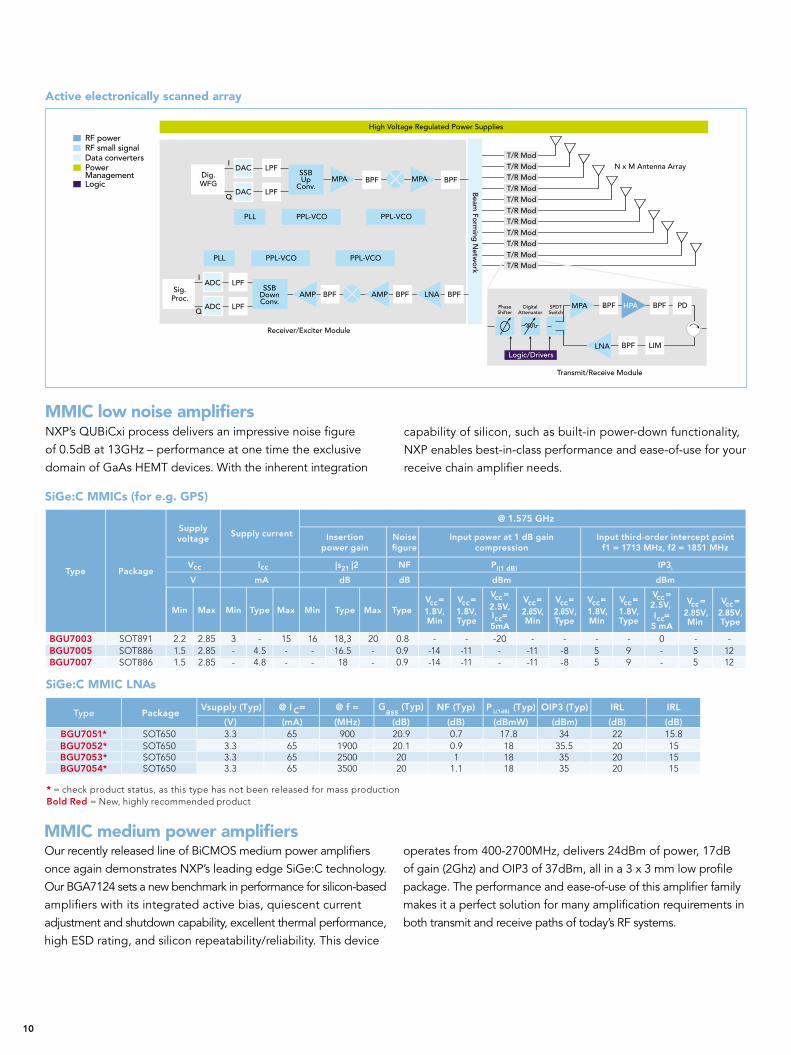
Active electronically scanned array
PPL-VCO PPL-VCOPLL
PPL-VCO PPL-VCOPLL
Dig.WFG
SSBUp
Conv.
N x M Antenna Array
Beam
Forming
Netw
ork
High Voltage Regulated Power Supplies
DAC
DAC
LPF
LPF
T/R ModT/R ModT/R ModT/R ModT/R ModT/R ModT/R ModT/R ModT/R ModT/R ModT/R Mod
DigitalAttenuator
SPDTSwitch
PhaseShifter
Sig.Proc.
SSBDownConv. MPA HPABPF BPF PD
LNA BPF LIM Logic/Drivers
MPA MPABPF BPF
AMP BPF LNA BPFBPFAMP
ADCI
Q
I
Q
ADC
LPF
LPF
Receiver/Exciter Module
Transmit/Receive Module
RF powerRF small signalData convertersPower ManagementLogic
PPL-VCO PPL-VCOPLL
PPL-VCO PPL-VCOPLL
Dig.WFG
SSBUp
Conv.
N x M Antenna Array
Beam
Forming
Netw
ork
High Voltage Regulated Power Supplies
DAC
DAC
LPF
LPF
T/R ModT/R ModT/R ModT/R ModT/R ModT/R ModT/R ModT/R ModT/R ModT/R ModT/R Mod
DigitalAttenuator
SPDTSwitch
PhaseShifter
Sig.Proc.
SSBDownConv. MPA HPABPF BPF PD
LNA BPF LIM Logic/Drivers
MPA MPABPF BPF
AMP BPF LNA BPFBPFAMP
ADCI
Q
I
Q
ADC
LPF
LPF
Receiver/Exciter Module
Transmit/Receive Module
RF powerRF small signalData convertersPower ManagementLogic
11
Low noise LO generators for VSAT applications
Type Package
fIN(REF) VCC ICC PLL phase noise @ N=64, @100kHz
PLL Output buffer Input
fo(RF) Po RLout(RF) Si
Typ Typ Max Typ Max Min
MHz V mA dBc/Hz GHz dBm dB dBm
TFF1003HN SOT616 50~815 3.3 100 -92 12.8~13.05 -5 -10 -10
TFF1007HN* SOT616 230.46~234.38 3.3 100 -104 14.75~15 -3 -10 -10
Low noise LO generators for general microwave applications
Type PackagefIN(REF)
VCC ICCPLL phase noise @
N=64PLL Output buffer Input
fo(RF) Po RLout(RF) STyp Typ @ 100kHz @ 10MHz Min Typ Max Typ Max Min
MHz V mA dBc/Hz dBc/Hz GHz GHz GHz dBm dB dBmTFF11070HN* SOT616 27 - 448 3.3 100 -95 -131 6.84 7.00 7.16 -5 -10 -10TFF11073HN* SOT616 28 - 468 3.3 100 -95 -131 7.16 7.33 7.49 -5 -10 -10TFF11077HN* SOT616 29 - 490 3.3 100 -95 -131 7.49 7.67 7.84 -5 -10 -10TFF11080HN* SOT616 31 - 513 3.3 100 -95 -131 7.84 8.02 8.21 -5 -10 -10TFF11084HN* SOT616 32 - 537 3.3 100 -95 -131 8.21 8.40 8.59 -5 -10 -10TFF11088HN* SOT616 34 - 562 3.3 100 -95 -131 8.59 8.79 8.99 -5 -10 -10TFF11092HN* SOT616 35 - 588 3.3 100 -95 -131 8.99 9.20 9.41 -5 -10 -10TFF11096HN* SOT616 37 - 616 3.3 100 -95 -131 9.41 9.63 9.85 -5 -10 -10TFF11101HN* SOT616 38 - 644 3.3 100 -95 -131 9.85 10.07 10.31 -5 -10 -10TFF11105HN* SOT616 40 - 674 3.3 100 -95 -131 10.31 10.54 10.79 -5 -10 -10TFF11110HN* SOT616 42 - 706 3.3 100 -95 -131 10.79 11.03 11.29 -5 -10 -10TFF11115HN* SOT616 44 - 738 3.3 100 -95 -131 11.29 11.55 11.81 -5 -10 -10TFF11121HN* SOT616 46 - 773 3.3 100 -95 -131 11.81 12.09 12.36 -5 -10 -10TFF11126HN* SOT616 48 - 809 3.3 100 -95 -131 12.36 12.65 12.94 -5 -10 -10TFF11139HN* SOT616 53 - 886 3.3 100 -95 -131 13.54 13.85 14.17 -5 -10 -10TFF11145HN* SOT616 55 - 927 3.3 100 -95 -131 14.17 14.50 14.83 -5 -10 -10TFF11152HN* SOT616 58 - 970 3.3 100 -95 -131 14.83 15.18 15.52 -5 -10 -10
* = check product status, as this type has not been released for mass productionBold Red = New, highly recommended product
* = check product status, as this type has not been released for mass productionBold Red = New, highly recommended product
SiGe:C MMIC LNAs
Type Package Vsupply (Typ) C L(1dB)
(V)
IRL
(dB)
IRL
(dB)
OIP3 (Typ)
(dBm)
P (Typ)
(dBmW)
NF (Typ)
(dB)
Gass (Typ)
(dB)
@ f =
(MHz)
@ I =
(mA)BGU7051* SOT650BGU7052* SOT650BGU7053* SOT650BGU7054* SOT650
* = check product status, as this type has not been released for mass productionBold Red = New, highly recommended product
3.3 65 900 20.9 0.7 17.8 34 22 15.8
3.3 65 3500 20 1.1 18 35 20 153.3 65 2500 20 1 18 35 20 153.3 65 1900 20.1 0.9 18 35.5 20 15
Medium power ampli�er MMICs for all 400 - 2700MHz applications
Supply Shutdown control RF performance RF performance
Type Package fVcc Icc VI(D)L(SHDN) VI(D)H(SHDN) II(D)L(SHDN) Typ @ f = 940MHz Typ @ f = 1960MHz
Typ Typ Max Min Max Min Max Typ Gp PL(1dB) OIP3 NF Gp PL(1dB) OIP3 NF MHz V mA mA V V V V µA dB dBm dBm dB dB dBm dBm dB
BGA7124 SOT908 leadless 400 - 2700 5 130 200 0 0.7 2.5 Vbias 4 22 25 38 5 16 24 38 5BGA7024 SOT89 leaded 400 - 2700 5 110 - - - - - - 22 24 38 3 16 25 38 4BGA7127 SOT908 leadless 400 - 2700 5 180 325 0 0.7 2.5 Vbias 4 20 28 44 3 13 28 43 5BGA7027 SOT89 leaded 400 - 2700 5 170 - - - - - - 19 28 41 3 12 28 43 4BGA6130* SOT908 leadless 100 - 1000 5 - - 0 0.7 2.5 Vbias 4 18 30 45 4 12 30 45 4BGA6133* SOT908 leadless 100 - 1000 5 - - 0 0.7 2.5 Vbias 4 18 33 46 4 12 33 47 4
SiGe:C MMICs (for e.g. GPS)
Type Package
Supply voltage
Supply current
@ 1.575 GHz
Insertion power gain
Noise �gure
Input power at 1 dB gain compression
Input third-order intercept pointf1 = 1713 MHz, f2 = 1851 MHz
Vcc Icc |s21 |2 NF PI(1 dB) IP3i
V mA dB dB dBm dBm
Min Max Min Type Max Min Type Max TypeVcc = 1.8V, Min
Vcc = 1.8V, Type
Vcc = 2.5V, Icc =5mA
Vcc = 2.85V, Min
Vcc = 2.85V, Type
Vcc = 1.8V, Min
Vcc = 1.8V, Type
Vcc = 2.5V, Icc =
5 mA Min
Vcc = 2.85V,
Vcc = 2.85V,
Type
i
BGU7003 SOT891 2.2 2.85 3 - 15 16 18,3 20 0.8 - - -20 - - - - 0 - -BGU7005 SOT886 1.5 2.85 - 4.5 - - 16.5 - 0.9 -14 -11 - -11 -8 5 9 - 5 12BGU7007 SOT886 1.5 2.85 - 4.8 - - 18 - 0.9 -14 -11 - -11 -8 5 9 - 5 12
MMIC variable gain amplifiersOur newest lines of MMICs are variable gain amplifiers designed for a wide attenuation range, broad frequency range and excellent linearity.
These VGAs are packaged in an industry standard SOT617 QFN package and provide excellent performance in a small footprint and low profile form factor.
SiGe:C MMICs variable gain ampli�ers
Type Package Control interfaceVsup Isup Frequency
Gain range
@ minimum attenuation @ maximum attenuation
Gain OIP3 NF Gain OIP3 NF(V) (mA) (MHz) (dB) (dB) (dBm) (dB) (dB) (dBm) (dB)
BGA7202* SOT617 Analog 5 710700 – 1450 27 24 45 6.5 -3 23.5 33.5
1450 – 2200 27 24 45 6.5 -3 23.5 33.5BGA7203* SOT617 Analog 5 710 2100 – 2750 27 24 45 6.5 -3 23.5 33.5BGA7204* SOT617 Parallel, serial 5 160 700 – 2750 31.5 24 37 6.5 -7.5 19 38BGA7350* SOT617 Parallel, digital 5 240
50 – 25024 18.5 - 6 -5.5 50 30
BGA7351* SOT617 Parallel, digital 5 240 28 18.5 - 6 -9.5 50 34
BGA7350 and BGA7351 are dual VGA products. The VGA function is twice on the chip.BGA7350 and BGA7351 are designed for receiving.
New features include flatter gain, a gain slope of 0.5dB, improved P1dB vs. Icc, without the need of an output inductor (also not at high P1dB models).
MMIC IF gain blocksFor compatibility with existing designs, the BGA28xx series uses a market standard package, the SOT363, and the pin-compliant SOT363F package. The pinning is identical to NXP’s current gainblock family, and the blocks deliver similar noise figures.
Quick reference to IF gain MMICs
Type Package
@ Fu @ 1 GHz Gain (dB) @
Vs Is @-3dB NF Gain OIP3 250 950 1550 2150
(V) (mA) (GHz) (dB) (dB) (dBm) (MHz) (MHz) (MHz) (MHz)
BGA280 SOT363 3.3 9.7 >3 3.4 20.2 11.5 20.0 20.2 20.6 20.6
BGA280 SOT363 3.3 12.4 3.0 3.6 22.1 13.6 22.3 22.1 23.0 23.8
BGA281 SOT363 3.3 16.4 >3 3.4 25.4 18.2 26.2 25.4 25.5 25.8
BGA281 SOT363 3.3 19.6 2.3 2.8 31.2 16.1 32.0 31.2 30.6 28.7
BGA285 SOT363 5.0 7.7 >3 3.9 23.3 8.7 22.9 23.2 23.9 24.0
BGA286 SOT363 5.0 22.7 2.6 3.7 31.9 20.9 31.2 31.8 32.6 31.4
BGA286 SOT363 5.0 15.4 >3 3.6 23.4 17.7 23.0 23.3 24.0 24.3
No output inductor necessary when using the new BGA28xx IF Gain blocks at the output stage.
12
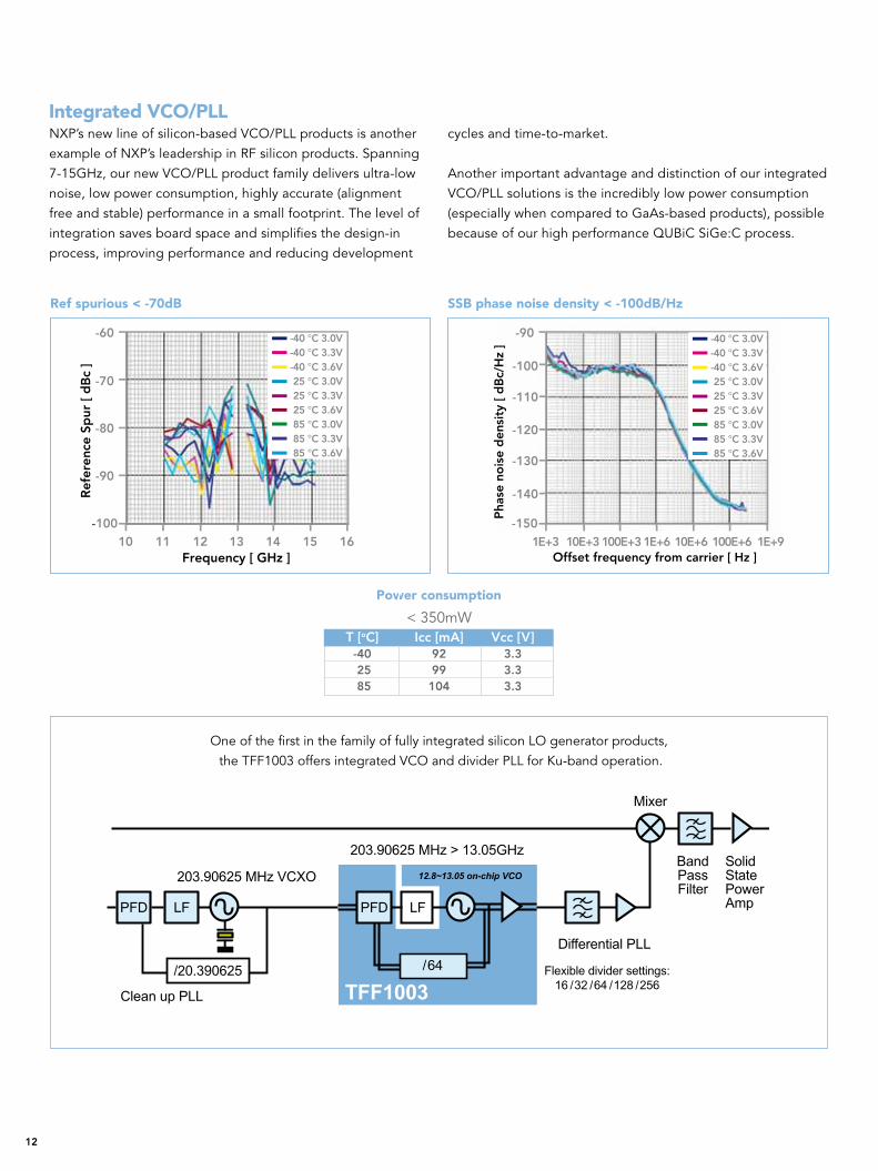
Ref spurious < -70dB
-40 ºC 3.0V -40 ºC 3.3V -40 ºC 3.6V 25 ºC 3.0V 25 ºC 3.3V 25 ºC 3.6V 85 ºC 3.0V 85 ºC 3.3V 85 ºC 3.6V
SSB phase noise density < -100dB/Hz
-40 ºC 3.0V -40 ºC 3.3V -40 ºC 3.6V 25 ºC 3.0V 25 ºC 3.3V 25 ºC 3.6V 85 ºC 3.0V 85 ºC 3.3V 85 ºC 3.6V
Power consumption
< 350mW T [oC] Icc [mA] Vcc [V] -40 92 3.3 25 99 3.3 85 104 3.3
One of the first in the family of fully integrated silicon LO generator products, the TFF1003 offers integrated VCO and divider PLL for Ku-band operation.
Integrated VCO/PLLNXP’s new line of silicon-based VCO/PLL products is another example of NXP’s leadership in RF silicon products. Spanning 7-15GHz, our new VCO/PLL product family delivers ultra-low noise, low power consumption, highly accurate (alignment free and stable) performance in a small footprint. The level of integration saves board space and simplifies the design-inprocess, improving performance and reducing development
cycles and time-to-market.
Another important advantage and distinction of our integrated VCO/PLL solutions is the incredibly low power consumption (especially when compared to GaAs-based products), possible because of our high performance QUBiC SiGe:C process.
13
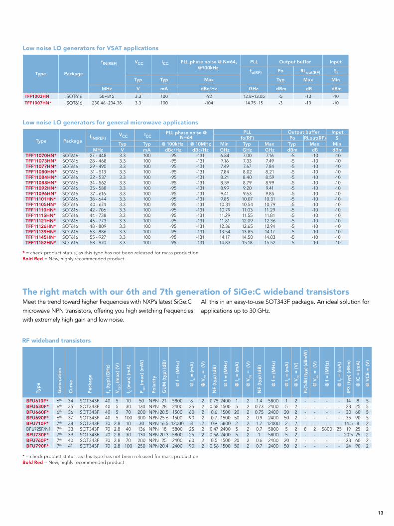
The right match with our 6th and 7th generation of SiGe:C wideband transistorsMeet the trend toward higher frequencies with NXP’s latest SiGe:C microwave NPN transistors, offering you high switching frequencies with extremely high gain and low noise.
All this in an easy-to-use SOT343F package. An ideal solution for applications up to 30 GHz.
RF wideband transistors
Typ
e
Ge
ne
rati
on
Cu
rve
Pac
kag
e
f T (t
yp) (
GH
z)
VC
EO (
max
) (V
)
I C (
max
) (m
A)
Pto
t (m
ax) (
mW
)
Po
lari
ty
GU
M (t
yp) (
dB
)
@ f
= (
MH
z)
@ I C
= (m
A)
@ V
CE =
(V
)
NF
(typ
) (d
B)
@ f
= (
MH
z)
@ I C
= (m
A)
@ V
CE =
(V
)
NF
(typ
) (d
B)
@ f
= (
MH
z)
@ I C
= (m
A)
@ V
CE =
(V
)
PL(1
dB) (
typ)
(dB
mW
)
@ V
CE =
(V
)
@ f
= (
MH
z)
@ I C
= (m
A)
IP3
(typ
) (d
Bm
)
@ IC
= (m
A)
@ V
CE
= (
V)
BFU610F* 6th 34 SOT343F 40 5 10 50 NPN 21 5800 8 2 0.75 2400 1 2 1.4 5800 1 2 - - - - 14 8 5BFU630F* 6th 35 SOT343F 40 5 30 130 NPN 28 2400 25 2 0.58 1500 5 2 0.73 2400 5 2 - - - - 23 25 5BFU660F* 6th 36 SOT343F 40 5 70 200 NPN 28.5 1500 60 2 0.6 1500 20 2 0.75 2400 20 2 - - - - 30 60 5BFU690F* 6th 37 SOT343F 40 5 100 300 NPN 25.6 1500 90 2 0.7 1500 50 2 0.9 2400 50 2 - - - - 35 90 5BFU710F* 7th 38 SOT343F 70 2.8 10 30 NPN 16.5 12000 8 2 0.9 5800 2 2 1.7 12000 2 2 - - - - 14.5 8 2BFU725F/N1 7th 33 SOT343F 70 2.8 40 136 NPN 18 5800 25 2 0.47 2400 5 2 0.7 5800 5 2 8 2 5800 25 19 25 2BFU730F* 7th 39 SOT343F 70 2.8 30 130 NPN 20.3 5800 25 2 0.56 2400 5 2 1 5800 5 2 - - - - 20.5 25 2BFU760F* 7th 40 SOT343F 70 2.8 70 200 NPN 25 2400 60 2 0.5 1500 20 2 0.6 2400 20 2 - - - - 23 60 2BFU790F* 7th 41 SOT343F 70 2.8 100 250 NPN 20.4 2400 90 2 0.56 1500 50 2 0.7 2400 50 2 - - - - 24 90 2
* = check product status, as this type has not been released for mass production Bold Red = New, highly recommended product
RF wideband transistors
Typ
e
Ge
ne
rati
on
Cu
rve
Pac
kag
e
f T (t
yp) (
GH
z)
VC
EO (
max
) (V
)
I C (
max
) (m
A)
Pto
t (m
ax) (
mW
)
Po
lari
ty
GU
M (t
yp) (
dB
)
@ f
= (
MH
z)
@ I C
= (m
A)
@ V
CE =
(V
)
NF
(typ
) (d
B)
@ f
= (
MH
z)
@ I C
= (m
A)
@ V
CE =
(V
)
NF
(typ
) (d
B)
@ f
= (
MH
z)
@ I C
= (m
A)
@ V
CE =
(V
)
PL(1
dB) (
typ)
(dB
mW
)
@ V
CE =
(V
)
@ f
= (
MH
z)
@ I C
= (m
A)
IP3
(typ
) (d
Bm
)
@ IC
= (m
A)
@ V
CE
= (
V)
BFG21W 5th 32 SOT343R - 4.5 500 600 NPN 10 1900 1 3.6 - - - - - - - - - - - - - - -BFG403W 5th 25 SOT343R 17 4.5 3.6 16 NPN 22 2000 3 2 1 900 1 2 1.6 2000 1 2 5 1 900 1 6 1 1BFG410W 5th 26 SOT343R 22 4.5 12 54 NPN 21 2000 10 2 0.9 900 1 2 1.2 2000 1 2 5 2 2000 10 15 10 2BFG424F 5th 27 SOT343F 25 4.5 30 135 NPN 23 2000 25 2 0.8 900 2 2 1.2 2000 2 2 12 2 2000 25 22 25 2BFG424W 5th 27 SOT343R 25 4.5 30 135 NPN 22 2000 25 2 0.8 900 2 2 1.2 2000 2 2 12 2 2000 25 22 25 2BFG425W 5th 27 SOT343R 25 4.5 30 135 NPN 20 2000 25 2 0.8 900 2 2 1.2 2000 2 2 12 2 2000 25 22 25 2BFG480W 5th 29 SOT343R 21 4.5 250 360 NPN 16 2000 80 2 1.2 900 8 2 1.8 2000 8 2 20 3.6 2000 1 28 80 2
BFU610F* 6th 34 SOT343F 40 5 10 50 NPN 21 5800 8 2 0.75 2400 1 2 1.4 5800 1 2 - - - - 14 8 5BFU630F* 6th 35 SOT343F 40 5 30 130 NPN 28 2400 25 2 0.58 1500 5 2 0.73 2400 5 2 - - - - 23 25 5BFU660F* 6th 36 SOT343F 40 5 70 200 NPN 28.5 1500 60 2 0.6 1500 20 2 0.75 2400 20 2 - - - - 30 60 5BFU690F* 6th 37 SOT343F 40 5 100 300 NPN 25.6 1500 90 2 0.7 1500 50 2 0.9 2400 50 2 - - - - 35 90 5BFU710F* 7th 38 SOT343F 70 2.8 10 30 NPN 16.5 12000 8 2 0.9 5800 2 2 1.7 12000 2 2 - - - - 14.5 8 2BFU725F/N1 7th 33 SOT343F 70 2.8 40 136 NPN 18 5800 25 2 0.47 2400 5 2 0.7 5800 5 2 8 2 5800 25 19 25 2BFU730F* 7th 39 SOT343F 70 2.8 30 130 NPN 20.3 5800 25 2 0.56 2400 5 2 1 5800 5 2 - - - - 20.5 25 2BFU760F* 7th 40 SOT343F 70 2.8 70 200 NPN 25 2400 60 2 0.5 1500 20 2 0.6 2400 20 2 - - - - 23 60 2BFU790F* 7th 41 SOT343F 70 2.8 100 250 NPN 20.4 2400 90 2 0.56 1500 50 2 0.7 2400 50 2 - - - - 24 90 2
* = check product status, as this type has not been released for mass production Bold Red = New, highly recommended product
Low noise LO generators for VSAT applications
Type Package
fIN(REF) VCC ICC PLL phase noise @ N=64, @100kHz
PLL Output buffer Input
fo(RF) Po RLout(RF) Si
Typ Typ Max Typ Max Min
MHz V mA dBc/Hz GHz dBm dB dBm
TFF1003HN SOT616 50~815 3.3 100 -92 12.8~13.05 -5 -10 -10
TFF1007HN* SOT616 230.46~234.38 3.3 100 -104 14.75~15 -3 -10 -10
Low noise LO generators for general microwave applications
Type PackagefIN(REF)
VCC ICCPLL phase noise @
N=64PLL Output buffer Input
fo(RF) Po RLout(RF) STyp Typ @ 100kHz @ 10MHz Min Typ Max Typ Max Min
MHz V mA dBc/Hz dBc/Hz GHz GHz GHz dBm dB dBmTFF11070HN* SOT616 27 - 448 3.3 100 -95 -131 6.84 7.00 7.16 -5 -10 -10TFF11073HN* SOT616 28 - 468 3.3 100 -95 -131 7.16 7.33 7.49 -5 -10 -10TFF11077HN* SOT616 29 - 490 3.3 100 -95 -131 7.49 7.67 7.84 -5 -10 -10TFF11080HN* SOT616 31 - 513 3.3 100 -95 -131 7.84 8.02 8.21 -5 -10 -10TFF11084HN* SOT616 32 - 537 3.3 100 -95 -131 8.21 8.40 8.59 -5 -10 -10TFF11088HN* SOT616 34 - 562 3.3 100 -95 -131 8.59 8.79 8.99 -5 -10 -10TFF11092HN* SOT616 35 - 588 3.3 100 -95 -131 8.99 9.20 9.41 -5 -10 -10TFF11096HN* SOT616 37 - 616 3.3 100 -95 -131 9.41 9.63 9.85 -5 -10 -10TFF11101HN* SOT616 38 - 644 3.3 100 -95 -131 9.85 10.07 10.31 -5 -10 -10TFF11105HN* SOT616 40 - 674 3.3 100 -95 -131 10.31 10.54 10.79 -5 -10 -10TFF11110HN* SOT616 42 - 706 3.3 100 -95 -131 10.79 11.03 11.29 -5 -10 -10TFF11115HN* SOT616 44 - 738 3.3 100 -95 -131 11.29 11.55 11.81 -5 -10 -10TFF11121HN* SOT616 46 - 773 3.3 100 -95 -131 11.81 12.09 12.36 -5 -10 -10TFF11126HN* SOT616 48 - 809 3.3 100 -95 -131 12.36 12.65 12.94 -5 -10 -10TFF11139HN* SOT616 53 - 886 3.3 100 -95 -131 13.54 13.85 14.17 -5 -10 -10TFF11145HN* SOT616 55 - 927 3.3 100 -95 -131 14.17 14.50 14.83 -5 -10 -10TFF11152HN* SOT616 58 - 970 3.3 100 -95 -131 14.83 15.18 15.52 -5 -10 -10
* = check product status, as this type has not been released for mass productionBold Red = New, highly recommended product
* = check product status, as this type has not been released for mass productionBold Red = New, highly recommended product
SiGe:C MMIC LNAs
Type Package Vsupply (Typ) C L(1dB)
(V)
IRL
(dB)
IRL
(dB)
OIP3 (Typ)
(dBm)
P (Typ)
(dBmW)
NF (Typ)
(dB)
Gass (Typ)
(dB)
@ f =
(MHz)
@ I =
(mA)BGU7051* SOT650BGU7052* SOT650BGU7053* SOT650BGU7054* SOT650
* = check product status, as this type has not been released for mass productionBold Red = New, highly recommended product
3.3 65 900 20.9 0.7 17.8 34 22 15.8
3.3 65 3500 20 1.1 18 35 20 153.3 65 2500 20 1 18 35 20 153.3 65 1900 20.1 0.9 18 35.5 20 15
Medium power ampli�er MMICs for all 400 - 2700MHz applications
Supply Shutdown control RF performance RF performance
Type Package fVcc Icc VI(D)L(SHDN) VI(D)H(SHDN) II(D)L(SHDN) Typ @ f = 940MHz Typ @ f = 1960MHz
Typ Typ Max Min Max Min Max Typ Gp PL(1dB) OIP3 NF Gp PL(1dB) OIP3 NF MHz V mA mA V V V V µA dB dBm dBm dB dB dBm dBm dB
BGA7124 SOT908 leadless 400 - 2700 5 130 200 0 0.7 2.5 Vbias 4 22 25 38 5 16 24 38 5BGA7024 SOT89 leaded 400 - 2700 5 110 - - - - - - 22 24 38 3 16 25 38 4BGA7127 SOT908 leadless 400 - 2700 5 180 325 0 0.7 2.5 Vbias 4 20 28 44 3 13 28 43 5BGA7027 SOT89 leaded 400 - 2700 5 170 - - - - - - 19 28 41 3 12 28 43 4BGA6130* SOT908 leadless 100 - 1000 5 - - 0 0.7 2.5 Vbias 4 18 30 45 4 12 30 45 4BGA6133* SOT908 leadless 100 - 1000 5 - - 0 0.7 2.5 Vbias 4 18 33 46 4 12 33 47 4
SiGe:C MMICs (for e.g. GPS)
Type Package
Supply voltage
Supply current
@ 1.575 GHz
Insertion power gain
Noise �gure
Input power at 1 dB gain compression
Input third-order intercept pointf1 = 1713 MHz, f2 = 1851 MHz
Vcc Icc |s21 |2 NF PI(1 dB) IP3i
V mA dB dB dBm dBm
Min Max Min Type Max Min Type Max TypeVcc = 1.8V, Min
Vcc = 1.8V, Type
Vcc = 2.5V, Icc =5mA
Vcc = 2.85V, Min
Vcc = 2.85V, Type
Vcc = 1.8V, Min
Vcc = 1.8V, Type
Vcc = 2.5V, Icc =
5 mA Min
Vcc = 2.85V,
Vcc = 2.85V,
Type
i
BGU7003 SOT891 2.2 2.85 3 - 15 16 18,3 20 0.8 - - -20 - - - - 0 - -BGU7005 SOT886 1.5 2.85 - 4.5 - - 16.5 - 0.9 -14 -11 - -11 -8 5 9 - 5 12BGU7007 SOT886 1.5 2.85 - 4.8 - - 18 - 0.9 -14 -11 - -11 -8 5 9 - 5 12
14
The C14AMS process, a 0.14μm, 55GHz RF-CMOS mixed signaltechnology, includes (flash) memories and delivers superior perfor-mance in data converters, audio applications, microcontrollers, and interfaces.
Our broad-based portfolio of design IP lets you choose from a wide selection of advanced functions. Along with our digital standard and I/O cells, we offer an extensive range of CMOS functions (processors, memories, interfaces, buses, data converters, PLLs, oscillators) and state-of-the-art RF function (VCOs, LNAs, PLLs, PAs, mixers, down converters, dividers, synthesizers).
You can select from several Customer-Owned Tooling (COT)business models and decide on the level of service you need.Our offerings can include complete design suites for COT design, design consultancy and DfT support, and fast prototyping that covers MPW runs, grinding/sawing, and sample assembly. We canalso provide design debug and modification (FIB), along with test development and product engineering. Life testing, failure analysis, and qualification are other options. All our wafer production, assembly, and test operations are conducted in-house, so you deal with one supplier, from start to finish.
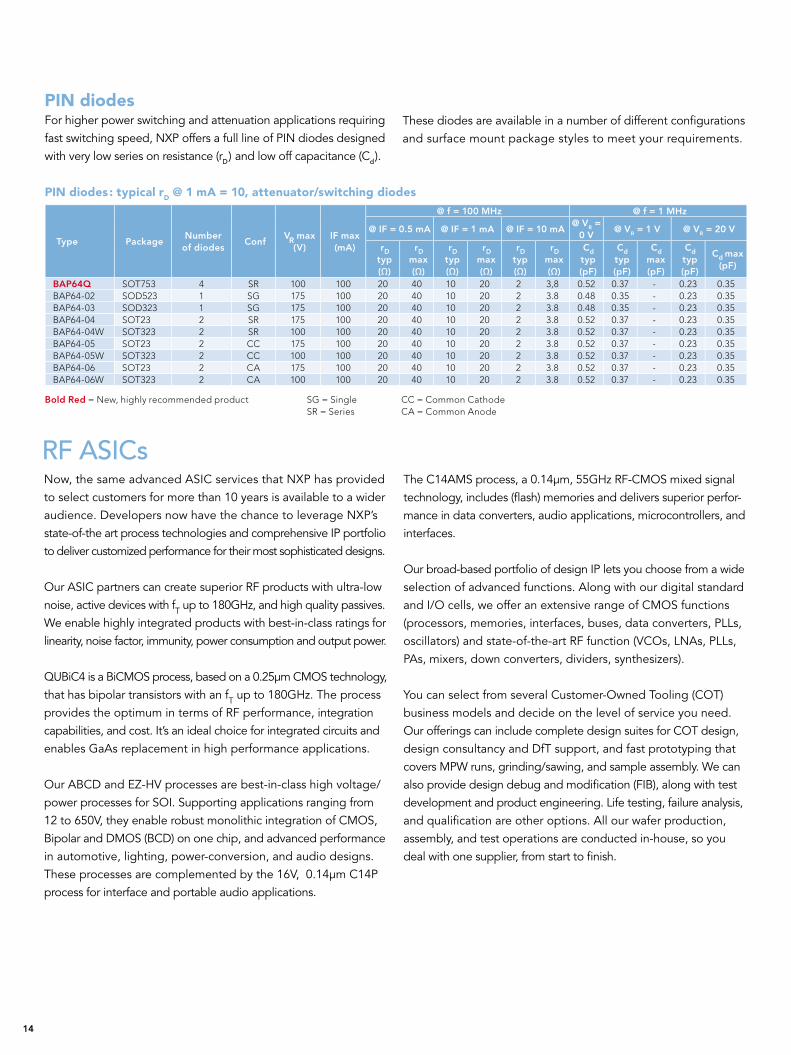
PIN diodesFor higher power switching and attenuation applications requiring fast switching speed, NXP offers a full line of PIN diodes designed with very low series on resistance (rD) and low off capacitance (Cd).
These diodes are available in a number of different configurations and surface mount package styles to meet your requirements.
PIN diodes : typical rD @ 1 mA = 10, attenuator/switching diodes
Type PackageNumber of diodes
ConfVR max
(V)IF max(mA)
@ f = 100 MHz @ f = 1 MHz
@ IF = 0.5 mA @ IF = 1 mA @ IF = 10 mA@ VR =
0 V@ VR = 1 V @ VR = 20 V
rDtyp(Ω)
rDmax(Ω)
rDtyp(Ω)
rDmax(Ω)
rDtyp(Ω)
rDmax(Ω)
Cdtyp(pF)
Cdtyp(pF)
Cd max(pF)
Cdtyp(pF)
Cd max(pF)
BAP64Q SOT753 4 SR 100 100 20 40 10 20 2 3,8 0.52 0.37 - 0.23 0.35BAP64-02 SOD523 1 SG 175 100 20 40 10 20 2 3.8 0.48 0.35 - 0.23 0.35BAP64-03 SOD323 1 SG 175 100 20 40 10 20 2 3.8 0.48 0.35 - 0.23 0.35BAP64-04 SOT23 2 SR 175 100 20 40 10 20 2 3.8 0.52 0.37 - 0.23 0.35BAP64-04W SOT323 2 SR 100 100 20 40 10 20 2 3.8 0.52 0.37 - 0.23 0.35BAP64-05 SOT23 2 CC 175 100 20 40 10 20 2 3.8 0.52 0.37 - 0.23 0.35BAP64-05W SOT323 2 CC 100 100 20 40 10 20 2 3.8 0.52 0.37 - 0.23 0.35BAP64-06 SOT23 2 CA 175 100 20 40 10 20 2 3.8 0.52 0.37 - 0.23 0.35BAP64-06W SOT323 2 CA 100 100 20 40 10 20 2 3.8 0.52 0.37 - 0.23 0.35
SG = Single CC = Common CathodeBold Red = New, highly recommended productSR = Series CA = Common Anode
Now, the same advanced ASIC services that NXP has providedto select customers for more than 10 years is available to a wideraudience. Developers now have the chance to leverage NXP’s state-of-the art process technologies and comprehensive IP portfolio to deliver customized performance for their most sophisticated designs.
Our ASIC partners can create superior RF products with ultra-low noise, active devices with fT up to 180GHz, and high quality passives.We enable highly integrated products with best-in-class ratings for linearity, noise factor, immunity, power consumption and output power.
QUBiC4 is a BiCMOS process, based on a 0.25μm CMOS technology, that has bipolar transistors with an fT up to 180GHz. The process provides the optimum in terms of RF performance, integration capabilities, and cost. It’s an ideal choice for integrated circuits and enables GaAs replacement in high performance applications.
Our ABCD and EZ-HV processes are best-in-class high voltage/power processes for SOI. Supporting applications ranging from12 to 650V, they enable robust monolithic integration of CMOS, Bipolar and DMOS (BCD) on one chip, and advanced performancein automotive, lighting, power-conversion, and audio designs. These processes are complemented by the 16V, 0.14μm C14P process for interface and portable audio applications.
RF ASICs
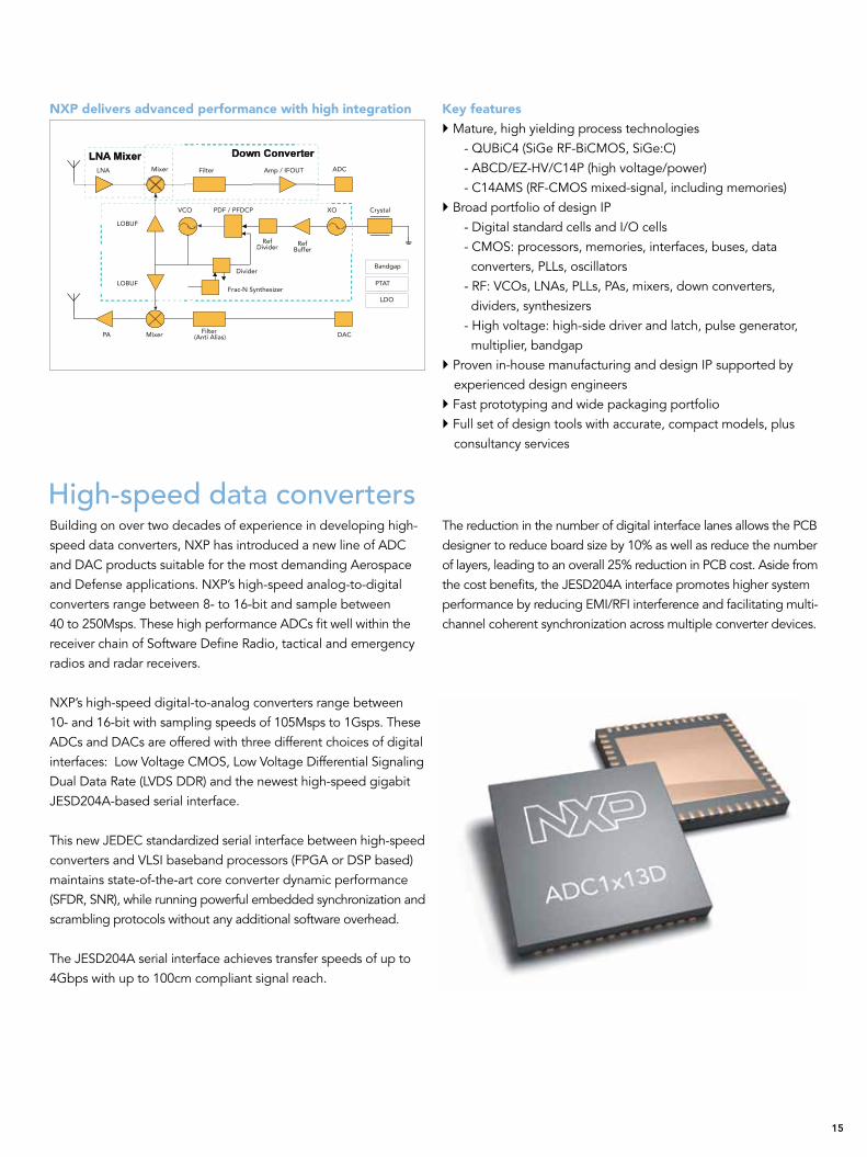
Building on over two decades of experience in developing high- speed data converters, NXP has introduced a new line of ADC and DAC products suitable for the most demanding Aerospace and Defense applications. NXP’s high-speed analog-to-digital converters range between 8- to 16-bit and sample between 40 to 250Msps. These high performance ADCs fit well within the receiver chain of Software Define Radio, tactical and emergency radios and radar receivers.
NXP’s high-speed digital-to-analog converters range between 10- and 16-bit with sampling speeds of 105Msps to 1Gsps. These ADCs and DACs are offered with three different choices of digital interfaces: Low Voltage CMOS, Low Voltage Differential Signaling Dual Data Rate (LVDS DDR) and the newest high-speed gigabit JESD204A-based serial interface.
This new JEDEC standardized serial interface between high-speed converters and VLSI baseband processors (FPGA or DSP based) maintains state-of-the-art core converter dynamic performance (SFDR, SNR), while running powerful embedded synchronization and scrambling protocols without any additional software overhead.
The JESD204A serial interface achieves transfer speeds of up to 4Gbps with up to 100cm compliant signal reach.
The reduction in the number of digital interface lanes allows the PCB designer to reduce board size by 10% as well as reduce the number of layers, leading to an overall 25% reduction in PCB cost. Aside fromthe cost benefits, the JESD204A interface promotes higher system performance by reducing EMI/RFI interference and facilitating multi-channel coherent synchronization across multiple converter devices.
High-speed data converters
15
NXP delivers advanced performance with high integration
LNA Mixer
Mixer
Filter Amp / IFOUT ADC
LOBUF
LOBUF
VCO PDF / PFDCP XO Crystal
RefBuffer
RefDivider
Divider
Frac-N Synthesizer
Bandgap
PTAT
LDO
DACFilter (Anti Alias)PA
Key features} Mature, high yielding process technologies - QUBiC4 (SiGe RF-BiCMOS, SiGe:C) - ABCD/EZ-HV/C14P (high voltage/power) - C14AMS (RF-CMOS mixed-signal, including memories)} Broad portfolio of design IP - Digital standard cells and I/O cells - CMOS: processors, memories, interfaces, buses, data converters, PLLs, oscillators - RF: VCOs, LNAs, PLLs, PAs, mixers, down converters, dividers, synthesizers - High voltage: high-side driver and latch, pulse generator, multiplier, bandgap} Proven in-house manufacturing and design IP supported by experienced design engineers} Fast prototyping and wide packaging portfolio} Full set of design tools with accurate, compact models, plus consultancy services
16
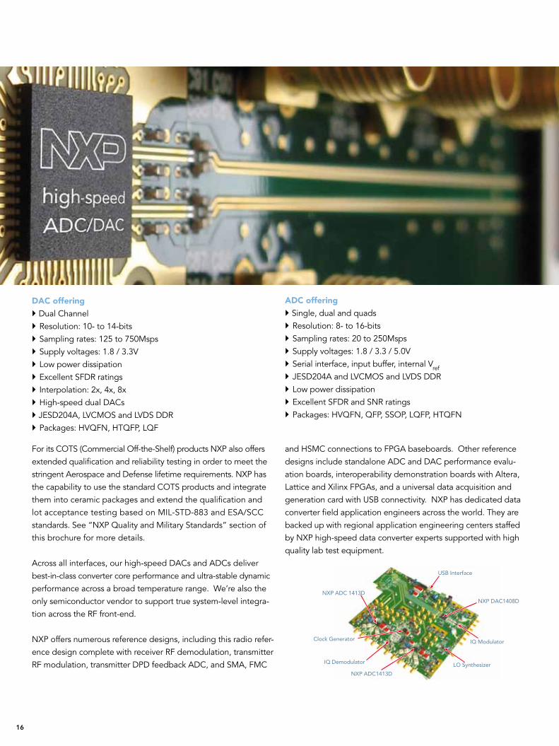
NXP ADC 1413D
USB Interface
NXP DAC1408D
IQ Modulator
LO Synthesizer
NXP ADC1413D
IQ Demodulator
Clock Generator
ADC offering} Single, dual and quads} Resolution: 8- to 16-bits} Sampling rates: 20 to 250Msps} Supply voltages: 1.8 / 3.3 / 5.0V} Serial interface, input buffer, internal Vref
} JESD204A and LVCMOS and LVDS DDR} Low power dissipation} Excellent SFDR and SNR ratings} Packages: HVQFN, QFP, SSOP, LQFP, HTQFN
DAC offering} Dual Channel} Resolution: 10- to 14-bits} Sampling rates: 125 to 750Msps} Supply voltages: 1.8 / 3.3V} Low power dissipation} Excellent SFDR ratings} Interpolation: 2x, 4x, 8x} High-speed dual DACs} JESD204A, LVCMOS and LVDS DDR} Packages: HVQFN, HTQFP, LQF
For its COTS (Commercial Off-the-Shelf) products NXP also offers extended qualification and reliability testing in order to meet the stringent Aerospace and Defense lifetime requirements. NXP has the capability to use the standard COTS products and integrate them into ceramic packages and extend the qualification and lot acceptance testing based on MIL-STD-883 and ESA/SCC standards. See “NXP Quality and Military Standards” section of this brochure for more details.
Across all interfaces, our high-speed DACs and ADCs deliver best-in-class converter core performance and ultra-stable dynamic performance across a broad temperature range. We’re also the only semiconductor vendor to support true system-level integra-tion across the RF front-end.
NXP offers numerous reference designs, including this radio refer-ence design complete with receiver RF demodulation, transmitter RF modulation, transmitter DPD feedback ADC, and SMA, FMC
and HSMC connections to FPGA baseboards. Other reference designs include standalone ADC and DAC performance evalu-ation boards, interoperability demonstration boards with Altera, Lattice and Xilinx FPGAs, and a universal data acquisition and generation card with USB connectivity. NXP has dedicated data converter field application engineers across the world. They are backed up with regional application engineering centers staffed by NXP high-speed data converter experts supported with high quality lab test equipment.
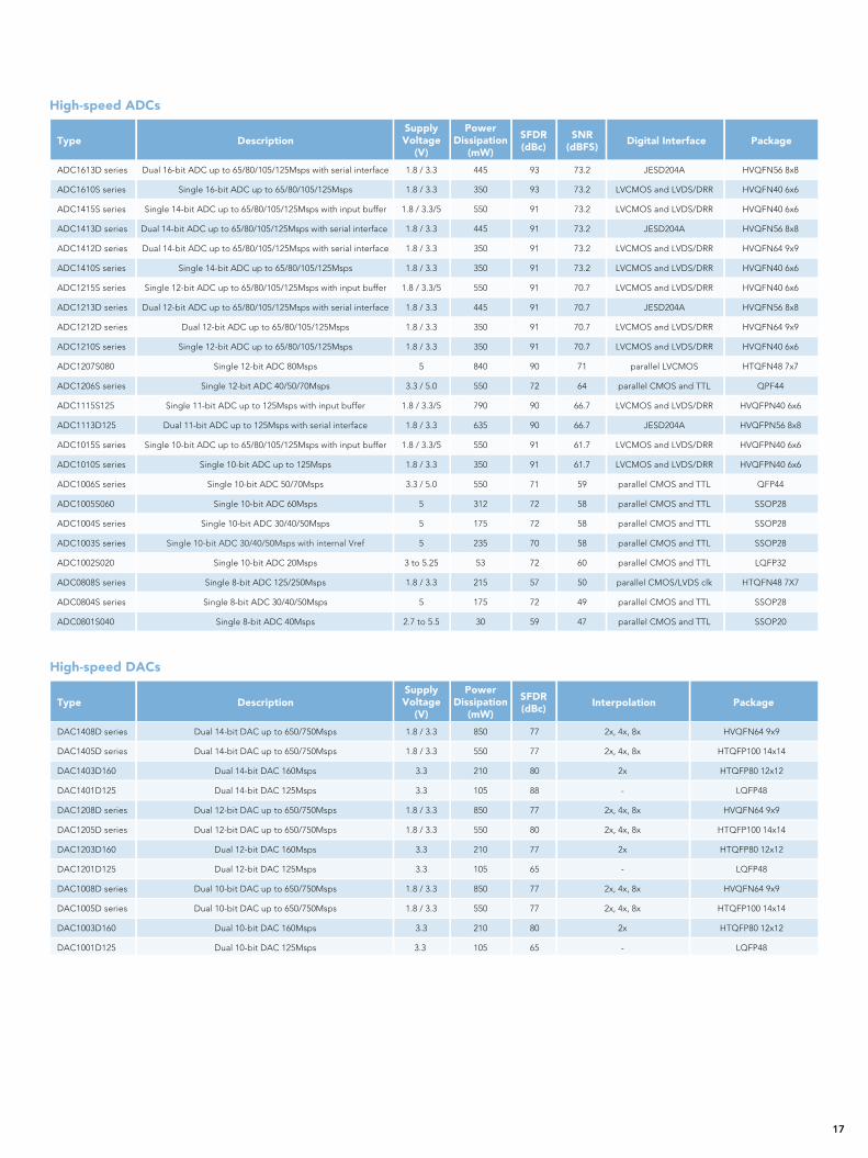
High-speed ADCs
Type Description Digital Interface PackageSupplyVoltage
(V)
PowerDissipation
(mW)
SFDR(dBc)
SNR(dBFS)
ADC1613D series Dual 16-bit ADC up to 65/80/105/125Msps with serial interface 1.8 / 3.3 445 93 73.2 JESD204A HVQFN56 8x8
ADC1610S series Single 16-bit ADC up to 65/80/105/125Msps 1.8 / 3.3 350 93 73.2 LVCMOS and LVDS/DRR HVQFN40 6x6
ADC1415S series Single 14-bit ADC up to 65/80/105/125Msps with input buffer 1.8 / 3.3/5 550 91 73.2 LVCMOS and LVDS/DRR HVQFN40 6x6
ADC1413D series Dual 14-bit ADC up to 65/80/105/125Msps with serial interface 1.8 / 3.3 445 91 73.2 JESD204A HVQFN56 8x8
ADC1412D series Dual 14-bit ADC up to 65/80/105/125Msps with serial interface 1.8 / 3.3 350 91 73.2 LVCMOS and LVDS/DRR HVQFN64 9x9
ADC1410S series Single 14-bit ADC up to 65/80/105/125Msps 1.8 / 3.3 350 91 73.2 LVCMOS and LVDS/DRR HVQFN40 6x6
ADC1215S series Single 12-bit ADC up to 65/80/105/125Msps with input buffer 1.8 / 3.3/5 550 91 70.7 LVCMOS and LVDS/DRR HVQFN40 6x6
ADC1213D series Dual 12-bit ADC up to 65/80/105/125Msps with serial interface 1.8 / 3.3 445 91 70.7 JESD204A HVQFN56 8x8
ADC1212D series Dual 12-bit ADC up to 65/80/105/125Msps 1.8 / 3.3 350 91 70.7 LVCMOS and LVDS/DRR HVQFN64 9x9
ADC1210S series Single 12-bit ADC up to 65/80/105/125Msps 1.8 / 3.3 350 91 70.7 LVCMOS and LVDS/DRR HVQFN40 6x6
ADC1207S080 Single 12-bit ADC 80Msps 5 840 90 71 parallel LVCMOS HTQFN48 7x7
ADC1206S series Single 12-bit ADC 40/50/70Msps 3.3 / 5.0 550 72 64 parallel CMOS and TTL QPF44
ADC1115S125 Single 11-bit ADC up to 125Msps with input buffer 1.8 / 3.3/5 790 90 66.7 LVCMOS and LVDS/DRR HVQFPN40 6x6
ADC1113D125 Dual 11-bit ADC up to 125Msps with serial interface 1.8 / 3.3 635 90 66.7 JESD204A HVQFPN56 8x8
ADC1015S series Single 10-bit ADC up to 65/80/105/125Msps with input buffer 1.8 / 3.3/5 550 91 61.7 LVCMOS and LVDS/DRR HVQFPN40 6x6
ADC1010S series Single 10-bit ADC up to 125Msps 1.8 / 3.3 350 91 61.7 LVCMOS and LVDS/DRR HVQFPN40 6x6
ADC1006S series Single 10-bit ADC 50/70Msps 3.3 / 5.0 550 71 59 parallel CMOS and TTL QFP44
ADC1005S060 Single 10-bit ADC 60Msps 5 312 72 58 parallel CMOS and TTL SSOP28
ADC1004S series Single 10-bit ADC 30/40/50Msps 5 175 72 58 parallel CMOS and TTL SSOP28
ADC1003S series Single 10-bit ADC 30/40/50Msps with internal Vref 5 235 70 58 parallel CMOS and TTL SSOP28
ADC1002S020 Single 10-bit ADC 20Msps 3 to 5.25 53 72 60 parallel CMOS and TTL LQFP32
ADC0808S series Single 8-bit ADC 125/250Msps 1.8 / 3.3 215 57 50 parallel CMOS/LVDS clk HTQFN48 7X7
ADC0804S series Single 8-bit ADC 30/40/50Msps 5 175 72 49 parallel CMOS and TTL SSOP28
ADC0801S040 Single 8-bit ADC 40Msps 2.7 to 5.5 30 59 47 parallel CMOS and TTL SSOP20
High-speed DACs
Type Description Interpolation PackageSupplyVoltage
(V)
PowerDissipation
(mW)
SFDR(dBc)
DAC1408D series Dual 14-bit DAC up to 650/750Msps 1.8 / 3.3 850 77 2x, 4x, 8x HVQFN64 9x9
DAC1405D series Dual 14-bit DAC up to 650/750Msps 1.8 / 3.3 550 77 2x, 4x, 8x HTQFP100 14x14
DAC1403D160 Dual 14-bit DAC 160Msps 3.3 210 80 2x HTQFP80 12x12
DAC1401D125 Dual 14-bit DAC 125Msps 3.3 105 88 - LQFP48
DAC1208D series Dual 12-bit DAC up to 650/750Msps 1.8 / 3.3 850 77 2x, 4x, 8x HVQFN64 9x9
DAC1205D series Dual 12-bit DAC up to 650/750Msps 1.8 / 3.3 550 80 2x, 4x, 8x HTQFP100 14x14
DAC1203D160 Dual 12-bit DAC 160Msps 3.3 210 77 2x HTQFP80 12x12
DAC1201D125 Dual 12-bit DAC 125Msps 3.3 105 65 - LQFP48
DAC1008D series Dual 10-bit DAC up to 650/750Msps 1.8 / 3.3 850 77 2x, 4x, 8x HVQFN64 9x9
DAC1005D series Dual 10-bit DAC up to 650/750Msps 1.8 / 3.3 550 77 2x, 4x, 8x HTQFP100 14x14
DAC1003D160 Dual 10-bit DAC 160Msps 3.3 210 80 2x HTQFP80 12x12
DAC1001D125 Dual 10-bit DAC 125Msps 3.3 105 65 - LQFP48
17
18
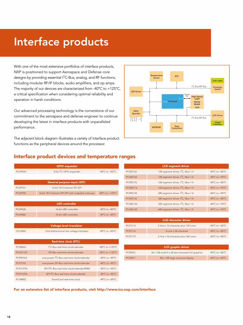
With one of the most extensive portfolios of interface products, NXP is positioned to support Aerospace and Defense core designs by providing essential I2C-Bus, analog, and RF functions, including modular RF/IF blocks, audio amplifiers, and op amps. The majority of our devices are characterized from -40ºC to +125ºC, a critical specification when considering optimal reliability and operation in harsh conditions.
Our advanced processing technology is the cornerstone of our commitment to the aerospace and defense engineer to continue developing the latest in interface products with unparalleled performance.
The adjacent block diagram illustrates a variety of interface product functions as the peripheral devices around the processor.
Interface products
XxXxXx
LED Driver
TemperatureSensor
RTC
ProximitySwitch
User Input
I2C Bus/SPI Bus
I2C Bus/SPI Bus
ParallelBus
VisualInterface
High-SpeedUART
RS232RS485
IrDA
EEPROM
LCD Driver
DataConverters
Processor
GPIO Epander
I2C/SPI
D[n:0]
PCA9554 8-bit I2C GPIO expander -40ºC to +85ºC
General purpose input (GPI)
LED controller
PCA9701 16-bit 18-V tolerant SPI GPI
PCA9703 16-bit 18-V tolerant SPI GPI with maskable interrupt -40ºC to +125ºC
PCA9635 16-bit LED controller -40ºC to +85ºC
PCA9685 16-bit LED controller -40ºC to +85ºC
Real-time clock (RTC)
PCA8565 I2C-Bus real-time clock/calendar -40ºC to +125ºC
PCA21125 SPI-Bus real-time clock/calendar -40ºC to +125ºC
PCF85163 Low-power I2C-Bus real-time clock/calendar -40ºC to +85ºC
PCF2123 Low-power SPI-Bus real-time clock/calendar -40ºC to +85ºC
PCF2127A SPI/I2C-Bus real-time clock/calendar/RAM -40ºC to +85ºC
PCF2129A SPI/I2C-Bus real-time clock/calendar -40ºC to +85ºC
PCA8802 SmartCard real-time clock -40ºC to +85ºC
LCD character driver
PCF2113 2-line x 12-character plus 120 icons
PCF2116 -40ºC to +85ºC
-40ºC to +85ºC
PCF85162 128 segment driver, I2C, Mux 1:4 -40ºC to +85ºC
PCA85162 128 segment driver, I2C, Mux 1:4 -40ºC to +95ºC
PCF85176 160 segment driver, I2C, Mux 1:4 -40ºC to +85ºC
PCA85176 160 segment driver, I2C, Mux 1:4 -40ºC to +95ºC
PCF85134 240 segment driver, I2C, Mux 1:4 -40ºC to +85ºC
PCF85133 320 segment driver, I2C, Mux 1:4 -40ºC to +85ºC
PCA85133 320 segment driver, I2C, Mux 1:4 -40ºC to +95ºC
PCA85132 640 segment driver, I2C, Mux 1:4 -40ºC to +95ºC
2-Line x 24-character
PCF2119 2-line x 16-character plus 160 icons -40ºC to +85ºC
LCD graphic driver
PCF8531 34 x 128 small 4 x 20 text character full graphics -40ºC to +85ºC
PCF8811 80 x 128 large universal display -40ºC to +85ºC
GPIO expander
GTL2002 2-bit bidirectional low voltage translator -40ºC to +85ºC
Voltage-level translator
LCD segment driver
Interface product devices and temperature ranges
For an extensive list of interface products, visit http://www.ics.nxp.com/interface
NXP Semiconductors has a broad portfolio of microcontroller solutions that complement Aerospace and Defense core designs by providing best-in-class embedded memory with many periph-eral options to meet every design need. Many of the devices are qualified to operate within an extended temperature range from -40˚C up to +125˚C and are designed to ensure reliable opera-tion under harsh conditions. NXP is committed to supporting the aerospace and defense system requirements and will continue to release new microcontroller products that leverage NXP’s most advanced processing technology to create best-in-class performance. From the smallest 8-bit to the highest performing 32-bit ARM microcontrollers, we drive the industry as an innovation
leader with our highly integrated and cost effective products. Our leading ARM9/ARM7-based LPC3000 and LPC2000 families have numerous, sophisticated integrated peripherals available. The industry’s fastest microcontrollers based on the low-power, cost-effective ARM Cortex-M3 and Cortex-M0 cores are part of our exciting new LPC1000 family, running at speeds of up to 100MHz and offering best-in-class performance and peripheral support. Our ARM-based LH7A and LH7 families feature high resolution integrated LCD controllers and provide System-on-Chip capability. Our established LPC900, LPC700, and 80C51 microcontroller families deliver solid 80C51-based performance. Be sure to visit our support section at www.nxp.com/microcontrollers
LPC3000 familyThe 32-bit LPC3000 family is based on the ARM926EJ core and is the only ARM9 microcontroller that provides a vector floating-point co-processor and integrated USB On-The-Go, as well as the ability
to operate in ultra-low power mode down to 0.9V. With speeds of up to 266MHz, the NXP LPC3000 family supports Linux and WinCE.
Microcontroller devices
LPC3000 family
The choice for embedded technologiesMemory Timers Serial interfaces Analog
Max
. fre
q. (
MH
z)
Type FLA
SH
RA
M
Inst
ruct
ion
cach
e
Dat
a ca
che
No
. of
tim
ers*
PW
M c
hann
els
Eth
erne
t
USB
UA
RT
I2 2
C
SPI
SSP
IS
AD
C (1
0-b
it)
No
. of
chan
-ne
ls
LCD
Co
ntro
ller/
Inte
rfac
e
SD/M
MC
I/O
pin
s
Ext
erna
l b
us in
terf
ace
PLL
CP
U v
olt
age
I/O
vo
ltag
e
Tem
p. r
ang
e o
pti
ons
Package Comments / special features
LPC3250 256 KB 32 KB 32 KB 8 11 1 1 7 2 2 2 2 3 • • 87 • • 266/ 208
1.35/ 1.2 V
1.8/ 2.8/ 3.0 V F LFBGA296
VFP unit, NAND Flash, SRAM/SDRAM/DDR, USB 2.0 FS OTG/Host/Device, 24-bit Color LCD controller and Touch Screen controller, Keypad interface and 0.9 V low power mode
LPC3240 256 KB 32 KB 32 KB 8 11 1 1 7 2 2 2 2 3 • 87 • • 266/ 208
1.35/ 1.2 V
1.8/ 2.8/ 3.0 V F LFBGA296 VFP unit, NAND Flash, SRAM/SDRAM/DDR, USB 2.0 FS OTG/Host/Device, Keypad
interface and 0.9 V low power mode
LPC3230 256 KB 32 KB 32 KB 8 11 1 7 2 2 2 2 3 • • 87 • • 266/ 208
1.35/ 1.2 V
1.8/ 2.8/ 3.0 V F LFBGA296
VFP unit, NAND Flash, SRAM/SDRAM/DDR, USB 2.0 FS OTG/Host/Device, 24-bit Color LCD controller and Touch Screen controller, Keypad interface and 0.9 V low power mode
LPC3220 128 KB 32 KB 32 KB 8 11 1 7 2 2 2 2 3 • 87 • • 266/ 208
1.35/ 1.2 V
1.8/ 2.8/ 3.0 V F LFBGA296 VFP unit, NAND Flash, SRAM/SDRAM/DDR, USB 2.0 FS OTG/Host/Device, Keypad
interface and 0.9 V low power mode
LPC3154 192 KB 16 KB 16 KB 4 1 1 1 1 1 1 3 • • 157 • • 180 1.2 V 1.8/ 2.8/ 3.3 V F TFBGA208 LPC3152 with a Decryption Engine & Secure Boot
LPC3152 192 KB 16 KB 16 KB 4 1 1 1 1 1 1 3 • • 157 • • 180 1.2 V 1.8/ 2.8/ 3.3 V F TFBGA208 Charger, Unique ID, OTP, HS USB 2.0 OTG with on-chip PHY, NAND Flash Controller,
MMC/SDHC/SDIO/CE-ATA, 6800/8080/Serial LCD Interface
LPC3143 192 KB 16 KB 16 KB 4 1 1 1 2 1 2 4 • • 97 • • 270 1.2 V 1.8/ 2.8/ 3.3 V F TFBGA180 LPC3141 with a Decryption Engine & Secure Boot
LPC3141 192 KB 16 KB 16 KB 4 1 1 1 2 1 2 4 • • 97 • • 270 1.2 V 1.8/ 2.8/ 3.3 V F TFBGA180 HS USB 2.0 OTG with on-chip PHY, NAND Flash Controller, MMC/SDHC/SDIO/CE-
ATA, 6800/8080 LCD Interface, Random Number Generator, Unique ID, OTP
LPC3131 192 KB 16 KB 16 KB 4 1 1 1 2 1 2 4 • • 97 • • 180 1.2 V 1.8/ 2.8/ 3.3 V F TFBGA180 LPC3130 with 192 KB SRAM
LPC3130 96 KB 16 KB 16 KB 4 1 1 1 2 1 2 4 • • 97 • • 180 1.2 V 1.8/ 2.8/ 3.3 V F TFBGA180 HS USB 2.0 OTG with on-chip PHY, NAND Flash Controller with 8-bit ECC, MMC/
SDHC/SDIO/CE-ATA, 6800/8080/Serial LCD Interface, Random Number Generator
LPC3180/01 64 KB 32 KB 32 KB 4 2 1 7 2 2 3 • 55 • • 208 1.2 V 1.8/ 2.8/ 3.0 V F LFBGA320 VFP unit, NAND Flash, SDRAM/DDR, USB 2.0 FS OTG/Host/Device
19
Microcontroller products
20
For an extensive list of all our micocontroller products and tools, visit http://www.ics.nxp.com/micrcontrollers
LPC1000 familyThe LPC1100 series, based on the ARM Cortex-M0, is the lowest priced 32-bit MCU solution on the market. It delivers unprecedent-ed performance, simplicity, low power, and dramatic reductions in
code size for every application. Based on the ARM Cortex-M3 core, operating at up to 120MHz, the LPC1700 series are low power 32-bit microcontrollers featuring a broad range of serial interfaces.
LPC1000 family
Memory Timers Serial interfaces Analog
Max
. fre
q. (M
Hz)
Tem
p. r
ange
op
tions
Type FLA
SH
RAM
No.
of t
imer
s*
PWM
cha
nnel
s
Ethe
rnet
USB
UA
RT
I2C
CA
N
SPI
SSP
I2S
AD
C c
hann
els/
reso
lutio
n
DA
C (1
0-bi
t)
No.
of c
han-
nels
SD/M
MC
I/O
pin
s
PLL
CPU
vol
tage
I/O
vol
tage
Package Comments / special features
LPC1700 devices
LPC1769 512 KB 64 KB 6 6 1 1 4 3 2 1 2 1 8 /12 b 1 70 • 120 3.3 V F LQFP100 120 MHz, 512 KB Flash with Ethernet, USB, CAN.
LPC1768 512 KB 64 KB 6 6 1 1 4 3 2 1 2 1 8 /12 b 1 70 • 100 3.3 V F LQFP100, TFBGA100 Cortex-M3 (Rev 2) version of LPC2368; adds NVIC, MPU, Motor Control PWM, QEI.
LPC1767 512 KB 64 KB 6 6 1 4 3 1 2 1 8 /12 b 1 70 • 100 3.3 V F LQFP100 512 K Flash with Ethernet
LPC1766 256 KB 64 KB 6 6 1 1 4 3 2 1 2 1 8 /12 b 1 70 • 100 3.3 V F LQFP100 256 K Flash version of LPC1768.
LPC1100 devices
LPC1114 32 KB 4-8 KB 5 13** 1 1 1-2 8 /10 b • 50 3.3 V F HVQFN33, LQFP48 Low cost, low power Cortex-M0 device
LPC1113 24 KB 4-8 KB 5 13** 1 1 1-2 8 /10 b • 50 3.3 V F HVQFN33, LQFP48 24 KB Flash version of LPC1114
LPC1112 16 KB 2-4 KB 5 13** 1 1 1 8 /10 b • 50 3.3 V F HVQFN33 16 KB Flash version of LPC1114
LPC1111 8 KB 2-4 KB 5 13** 1 1 1 8 /10 b • 50 3.3 V F HVQFN33 8 KB Flash version of LPC1114
LPC1765 256 KB 64 KB 6 6 1 4 3 2 1 2 1 8 /12 b 1 70 • 100 3.3 V F LQFP100 Same as LPC1766, but no Ethernet.
LPC1764 128 KB 32 KB 6 6 1 1 4 3 2 1 2 8 /12 b 70 • 100 3.3 V F LQFP100 128 K Flash / 32 K RAM version of LPC1766; USB Device only; no I2S, no DAC.
LPC1759 512 KB 64 KB 6 6 1 4 2 2 1 2 1 6 /12 b 1 52 • 120 3.3 V F LQFP80 120 MHz, 512 KB Flash with USB and CAN, 80-pin package.
LPC1758 512 KB 64 KB 6 6 1 1 4 2 2 1 2 1 6 /12 b 1 52 • 100 3.3 V F LQFP80 80-pin version of LPC1768 with 6-channels ADC in LQFP80.
LPC1756 256 KB 32 KB 6 6 1 4 2 2 1 2 1 6 /12 b 1 52 • 100 3.3 V F LQFP80 256 K Flash / 32 K RAM version of LPC1758; no Ethernet.
LPC1754 128 KB 32 KB 6 6 1 4 2 1 1 2 6 /12 b 1 52 • 100 3.3 V F LQFP80 128 K Flash version of LPC1756; 1 CAN only, no I2S.
LPC1752 64 KB 16 KB 6 6 1 4 2 1 1 2 6 /12 b 52 • 100 3.3 V F LQFP80 64 K Flash / 16 K RAM version of LPC1754; USB Device only, no DAC.
LPC1751 32 KB 8 KB 6 6 1 4 2 1 1 2 6 /12 b 52 • 100 3.3 V F LQFP80 32 K Flash / 8 K RAM version of LPC1752.
28 - 42
28 - 42
28
28
LPC11C00 devices
LPC11C12 16 KB 8 KB 5 13** 1 1 2 8 /10 b • 50 3.3 V F LQFP48 Cortex-M0 MCU with on-chip CAN drivers
LPC11C14 32 KB 8 KB 5 13** 1 1
1
1 2 8 /10 b • 50 3.3 V F LQFP48 32K Flash version of the LPC11C12
42
42
* Includes Watchdog timer and real-time clock. ** Using timers 0-3.
NXP offers a wide variety of AC-DC power conversion controllers and regulators. We have flyback controllers, resonant controllers and
secondary side controllers that provide the ultimate in efficiency and very low stand-by powers.
Key features} Integrated power factor correction (PFC) controller and flyback controller} High level of integration, low external component count} High voltage start-up current source} Wide VCC range (38V)} Fast latch reset function implemented, enabling fast recovery by mains interrupt} Soft (re)start for both flyback and PFC controller} Mains under-voltage and brown-out protection integrated
Flyback controller} Zero voltage switching} Quasi-resonant operation with frequency limitation} Frequency reduction at low loads
Power factor controller} Switches off automatically at standby/low power mode (controlled by flyback controller)} Dedicated circuitry built in to prevent audible noise during low power mode
Power management products
21
Power solution product highlightGreenChipTM III is the third generation of green Switched Mode Power Supply (SMPS) controller ICs. The TEA1751 combines a controller for Power Factor Correction (PFC) and a flyback controller. Its high level of integration allows the design of compact, high
efficiency power supplies with a very low number of external com- ponents. GreenChip™ III controllers are an excellent choice for power supplies up to about 250W.
Description Topology Soft startfosc
[max](kHz)
VCC[max]
Overloadprotection
Type
TEA1610P
TEA1610T
TEA1611T
TEA1713T
TEA1733AT
TEA1733LT
TEA1733P
TEA1733T
TEA1750T
TEA1751LT
TEA1751T
TEA1752LT
TEA1752T
TEA1761T
TEA1762T
TEA1791AT
TEA1791T
Resonant
Resonant
Resonant
Resonant+PFC
FF Flyback
FF Flyback
FF Flyback
FF Flyback
QR PFC + QR Flyback
QR PFC + QR Flyback
QR PFC + QR Flyback
QR PFC + QR Flyback
QR PFC + QR Flyback
Synchronous Recti�cation
Synchronous Recti�cation
Synchronous Recti�cation
Synchronous Recti�cation
500
500
500
500
90
67
67
67
125 (PFC) / 125 (Flyback)
125 (PFC) / 125 (Flyback)
125 (PFC) / 125 (Flyback)
250 (PFC) / 125 (Flyback)
250 (PFC) / 125 (Flyback)
500
500
500
500
15
15
20
38
30 (35V < 100msec)
30 (35V < 100msec)
30 (35V < 100msec)
30 (35V < 100msec)
38
38
38
38
38
38
38
38
38
Latched
Latched
Latched
Latched
Safe Restart
Latched
Safe Restart
Safe Restart
Safe Restart
Safe Restart
Latched
Safe Restart
Latched
No
No
Yes
Yes
Yes
Yes
Yes
Yes
Yes (PFC) / Yes (Flyback)
Yes (PFC) / Yes (Flyback)
Yes (PFC) / Yes (Fl yback)
Yes (PFC) / Yes (Flyback)
Yes (PFC) / Yes (Flyback)
Zero-voltage-switching resonant converter controller
Zero-voltage-switching resonant converter controller
Zero-voltage-switching resonant converter controller
GreenChipTM Resonant; LLC+PFC controller
GreenChipTM III Low Power, Flyback controller
GreenChipTM III Low Power, Flyback controller
GreenChipTM III Low Power, Flyback controller
GreenChipTM III Low Power, Flyback controller
GreenChipTM III, PFC + Flyback controller
GreenChipTM III, PFC + Flyback controller
GreenChipTM III, PFC + Flyback controller
GreenChipTM III, PFC + Flyback controller
GreenChipTM III, PFC + Flyback controller
GreenChipTM SR, Sync. Rec. control + feedback
GreenChipTM SR, Sync. Rec. control + feedback
GreenChipTM SR, Sync. Rec. control
GreenChipTM SR, Sync. Rec. control
DIP16
SO16
SO20
SO24
SO8
SO8
SO8
SO16
SO16
SO16
SO16
SO16
SO8
SO14
SO8
SO8
SOT38-1
SOT109-1
SOT163-1
SOT137-1
SOT96-1
SOT96-1
SOT96-1
SOT109-1
SOT109-1
SOT109-1
SOT109-1
SOT109-1
SOT96-1
SOT108-1
SOT96-1
SOT96-1
Package
DIP8
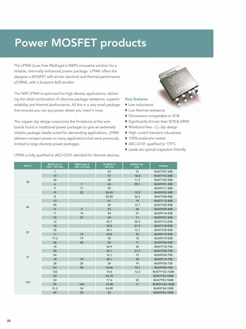
22
GPIO expanderVDS (V) Package
RDson max @VGS = 10V (mΩ)
RDson max @VGS = 5V (mΩ)
ID (MAX) @25ºC (A)
QG(tot) Typ(nC)
30
40
55
75
100
30
40
55
75
100
7102069
198
13258
112412183511
17.336182854182853
102335399
31.249
71122
91427
121940
193058
1043453
6347286359
26.6558.85
4125534024
43.733.520.143.83226
34.925.115.134.124
14.6610.6
24.7817.6
10.4824.89
23
3118.811.228.1
10.536.319
12.1302111
35.221.913.132181135
21.2123019
10.712.2
2211
BUK7Y07-30BBUK7Y10-30BBUK7Y20-30BBUK9Y07-30BBUK9Y11-30BBUK9Y22-30BBUK7Y08-40BBUK7Y13-40BBUK7Y25-40BBUK9Y09-40BBUK9Y14-40BBUK9Y27-40BBUK7Y12-55BBUK7Y18-55BBUK7Y35-55BBUK9Y12-55BBUK9Y19-55BBUK9Y40-55BBUK7Y18-75BBUK7Y28-75BBUK9Y54-75BBUK9Y19-75BBUK9Y30-75BBUK9Y58-75B
BUK7Y102-100BBUK7Y33-100BBUK7Y53-100B
BUK9Y104-100BBUK9Y34-100BBUK9Y53-100B
GPIO expander
The LFPAK (Loss Free PAcKage) is NXP’s innovative solution for a reliable, thermally enhanced power package. LFPAK offers the designer a MOSFET with similar electrical and thermal performance of DPAK, with a footprint 46% smaller.
The NXP LFPAK is optimized for high density applications, deliver-ing the ideal combination of ultra-low package resistance, superior reliability and thermal performance. All this in a very small package that ensures you can put power where you need it most.
The copper clip design overcomes the limitations of the wire bonds found in traditional power packages to give an extremelyreliable package ideally suited for demanding applications. LFPAKdelivers compact power to many applications that were previouslylimited to large discrete power packages.
LFPAK is fully qualified to AEC-Q101 standard for discrete devices.
Key features} Low inductance} Low thermal resistance} Dimensions comparable to SO8} Significantly thinner than SO8 & DPAK} Wirebond free - Cu clip design} High current transient robustness} 100% avalanche tested} AEC-Q101 qualified to 175°C} Leads are optical-inspection friendly
Power MOSFET products
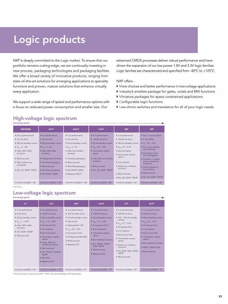
NXP is deeply committed to the Logic market. To ensure that our portfolio remains cutting-edge, we are continually investing in new process, packaging technologies and packaging facilities. We offer a broad variety of innovative products, ranging from state-of–the-art solutions for emerging applications to specialty functions and proven, mature solutions that enhance virtually every application.
We support a wide range of speed and performance options with a focus on reduced power consumption and smaller size. Our
advanced CMOS processes deliver robust performance and have driven the expansion of our low power 1.8V and 3.3V logic families.Logic families are characterized and specified from -40ºC to +125ºC.
NXP offers -} More choices and better performance in low-voltage applications} Industry’s smallest package for gates, octals and MSI functions} Miniature packages for space constrained applications} Configurable logic functions} Low-ohmic switches and translators for all of your logic needs
High-voltage logic spectrum
HEF4000B
Increasing speed
HC/T AHC/T FAST ABT CBT
� 60 ns performance*
� ±3 mA drive*
� 600 µA standby current
� VCC: 5 – 15V
� Gate, MSI, buffer functions
� Multi-sourced
� NXP number one worldwide
� DIL, SO, SSOP, TSSOP
Function available = 85
* At 15 V VCC
� 9 ns performance
� ±8 mA drive
� 80 µA standby current
� VCC: 2 – 6V
� Gate, MSI, buffer functions
� Analog switch functions
� PicoGate packaging
� MicroPak packaging
� SO,TSSOP, DQFN
� Multi-sourced
Function available = 321
� 5 ns performance
� ±8 mA drive
� 40 µA standby current
� VCC: 2 – 6V
� Gate, bus interface functions
� PicoGate packaging
� Multi-sourced
� SO,TSSOP, DQFN
� Replaces VHC/T
� MicroPak packaging
Function available = 105
� 4 ns performance
� -15/24 mA drive
� 90 µA standby current
� VCC: 4.5 – 5.5V
� Termination resistor option
� Gate, MSI, bus interface functions
� DIL, SO, SSOP, TSSOP
� Multi-sourced
Function available = 80 Function available = 64
� 3 ns performance
� -32/64 mA drive
� 250 µA standby current
� VCC: 4.5 – 5.5V
� Bus hold option
� Live insertion
� Termination resistor option
� Gates, bus, interface functions
� Multi-sourced
� DIL, SO, SSOP, TSSOP
Function available = 30
� Sub 1 ns prop delays
� 5 ohm RON
� VCC: 4.5 – 5.5V
� For circuit isolation and switching
� Schottky or charge pump undershoot protection
� Percharge circuit for hot plugging
� Internal diode for level shifting
� DIL, SO, SSOP, TSSOP
� Multi-sourced
LV
Increasing speed
LVC AUP ALVC LVT ALVT
� 9 ns performance
� 8 mA drive
� 20 µA standby current
� VCC: 1 – 3.6V*
� Gate, MSI, buffer functions
� SO, SSOP, TSSOP
� Multi-sourced
� SO, TSSOP, PicoGate DQFN
� MicroPak
� Replaces LCX
Function available = 46
* LV: some functions can operate up to 5.5V ** AVLC: only non-bus hold types are 5V input tolerant
� 4 ns performance
� -24/24 mA drive
� 20 µA standby current
� VCC: 1.2 – 3.6V*
� 5V tolerant I/O’s
� Live insertion
� 4 ns performance
� -4/4 mA static drive
� Optimized for 1.8V
� VCC: 0.8 – 3.6V
� Bus hold option
� Termination resistor option
� Multi-sourced
� Gates, MSI, bus interface functions
Function available = 137
� 0.9 µA standby current
� Cpd 4.5 pF
� 3.6 tolerant I/O’s
� PicoGate and MicroPak
� Replaces ULP
� Multi-sourced
Function available = 57
� 2 ns performance
� -24/24 mA drive
� 40 µA standby current
� VCC: 1.2 – 3.6V
� 5 V tolerant I/O’s**
� Bus hold option
� Termination resistor option
� SO, VSSOP, TSSOP BGA, DQFN
� Bus interface functions
� Multi-sourced
� Replaces VCX
Function available = 54 Function available = 44
� 2 ns performance
� -32/64 mA drive
� 120 – 190 µA standby current
� VCC: 2.7 – 3.6V
� Multi-sourced
� 5V tolerant I/O’s
� Termination resistor option
� Live insertion
� Built-in bus hold
� SO, SSOP, BGA, TSSOP, DQFN
� Gates, bus interface functions
Function available = 23
� 1.5 ns performance
� 32/64 mA drive
� 90 µA standby current
� VCC: 2.3 – 3.6V
� Live insertion
� Built-in bus hold
� Termination resistor option
� 5V tolerant I/O’s
� Bus interface functions
� Multi-sourced
� SSOP, TSSOP, BGA
Low-voltage logic spectrum
HEF4000B
Increasing speed
HC/T AHC/T FAST ABT CBT
� 60 ns performance*
� ±3 mA drive*
� 600 µA standby current
� VCC: 5 – 15V
� Gate, MSI, buffer functions
� Multi-sourced
� NXP number one worldwide
� DIL, SO, SSOP, TSSOP
Function available = 85
* At 15 V VCC
� 9 ns performance
� ±8 mA drive
� 80 µA standby current
� VCC: 2 – 6V
� Gate, MSI, buffer functions
� Analog switch functions
� PicoGate packaging
� MicroPak packaging
� SO,TSSOP, DQFN
� Multi-sourced
Function available = 321
� 5 ns performance
� ±8 mA drive
� 40 µA standby current
� VCC: 2 – 6V
� Gate, bus interface functions
� PicoGate packaging
� Multi-sourced
� SO,TSSOP, DQFN
� Replaces VHC/T
� MicroPak packaging
Function available = 105
� 4 ns performance
� -15/24 mA drive
� 90 µA standby current
� VCC: 4.5 – 5.5V
� Termination resistor option
� Gate, MSI, bus interface functions
� DIL, SO, SSOP, TSSOP
� Multi-sourced
Function available = 80 Function available = 64
� 3 ns performance
� -32/64 mA drive
� 250 µA standby current
� VCC: 4.5 – 5.5V
� Bus hold option
� Live insertion
� Termination resistor option
� Gates, bus, interface functions
� Multi-sourced
� DIL, SO, SSOP, TSSOP
Function available = 30
� Sub 1 ns prop delays
� 5 ohm RON
� VCC: 4.5 – 5.5V
� For circuit isolation and switching
� Schottky or charge pump undershoot protection
� Percharge circuit for hot plugging
� Internal diode for level shifting
� DIL, SO, SSOP, TSSOP
� Multi-sourced
LV
Increasing speed
LVC AUP ALVC LVT ALVT
� 9 ns performance
� 8 mA drive
� 20 µA standby current
� VCC: 1 – 3.6V*
� Gate, MSI, buffer functions
� SO, SSOP, TSSOP
� Multi-sourced
� SO, TSSOP, PicoGate DQFN
� MicroPak
� Replaces LCX
Function available = 46
* LV: some functions can operate up to 5.5V ** AVLC: only non-bus hold types are 5V input tolerant
� 4 ns performance
� -24/24 mA drive
� 20 µA standby current
� VCC: 1.2 – 3.6V*
� 5V tolerant I/O’s
� Live insertion
� 4 ns performance
� -4/4 mA static drive
� Optimized for 1.8V
� VCC: 0.8 – 3.6V
� Bus hold option
� Termination resistor option
� Multi-sourced
� Gates, MSI, bus interface functions
Function available = 137
� 0.9 µA standby current
� Cpd 4.5 pF
� 3.6 tolerant I/O’s
� PicoGate and MicroPak
� Replaces ULP
� Multi-sourced
Function available = 57
� 2 ns performance
� -24/24 mA drive
� 40 µA standby current
� VCC: 1.2 – 3.6V
� 5 V tolerant I/O’s**
� Bus hold option
� Termination resistor option
� SO, VSSOP, TSSOP BGA, DQFN
� Bus interface functions
� Multi-sourced
� Replaces VCX
Function available = 54 Function available = 44
� 2 ns performance
� -32/64 mA drive
� 120 – 190 µA standby current
� VCC: 2.7 – 3.6V
� Multi-sourced
� 5V tolerant I/O’s
� Termination resistor option
� Live insertion
� Built-in bus hold
� SO, SSOP, BGA, TSSOP, DQFN
� Gates, bus interface functions
Function available = 23
� 1.5 ns performance
� 32/64 mA drive
� 90 µA standby current
� VCC: 2.3 – 3.6V
� Live insertion
� Built-in bus hold
� Termination resistor option
� 5V tolerant I/O’s
� Bus interface functions
� Multi-sourced
� SSOP, TSSOP, BGA
23
Logic products
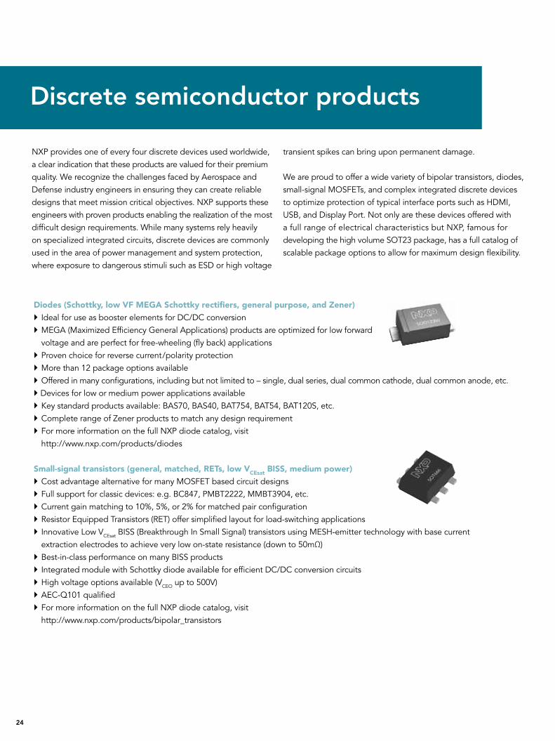
24
Diodes (Schottky, low VF MEGA Schottky rectifiers, general purpose, and Zener) } Ideal for use as booster elements for DC/DC conversion} MEGA (Maximized Efficiency General Applications) products are optimized for low forward voltage and are perfect for free-wheeling (fly back) applications} Proven choice for reverse current/polarity protection} More than 12 package options available} Offered in many configurations, including but not limited to – single, dual series, dual common cathode, dual common anode, etc.} Devices for low or medium power applications available } Key standard products available: BAS70, BAS40, BAT754, BAT54, BAT120S, etc.} Complete range of Zener products to match any design requirement} For more information on the full NXP diode catalog, visit http://www.nxp.com/products/diodes
Small-signal transistors (general, matched, RETs, low VCEsat BISS, medium power) } Cost advantage alternative for many MOSFET based circuit designs } Full support for classic devices: e.g. BC847, PMBT2222, MMBT3904, etc.} Current gain matching to 10%, 5%, or 2% for matched pair configuration } Resistor Equipped Transistors (RET) offer simplified layout for load-switching applications} Innovative Low VCEsat BISS (Breakthrough In Small Signal) transistors using MESH-emitter technology with base current extraction electrodes to achieve very low on-state resistance (down to 50mΩ) } Best-in-class performance on many BISS products} Integrated module with Schottky diode available for efficient DC/DC conversion circuits } High voltage options available (VCEO up to 500V)} AEC-Q101 qualified} For more information on the full NXP diode catalog, visit http://www.nxp.com/products/bipolar_transistors
NXP provides one of every four discrete devices used worldwide, a clear indication that these products are valued for their premium quality. We recognize the challenges faced by Aerospace and Defense industry engineers in ensuring they can create reliable designs that meet mission critical objectives. NXP supports these engineers with proven products enabling the realization of the most difficult design requirements. While many systems rely heavily on specialized integrated circuits, discrete devices are commonly used in the area of power management and system protection, where exposure to dangerous stimuli such as ESD or high voltage
transient spikes can bring upon permanent damage.
We are proud to offer a wide variety of bipolar transistors, diodes, small-signal MOSFETs, and complex integrated discrete devices to optimize protection of typical interface ports such as HDMI, USB, and Display Port. Not only are these devices offered with a full range of electrical characteristics but NXP, famous for developing the high volume SOT23 package, has a full catalog of scalable package options to allow for maximum design flexibility.
Discrete semiconductor products
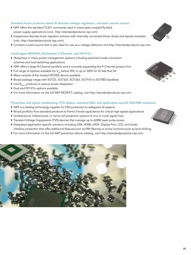
Standard linear products (shunt & discrete voltage regulators, constant current source)} NXP offers the standard TL431 commonly used in many opto-coupled fly-back power supply applications (visit, http://standardproducts.nxp.com)} Inexpensive discrete linear regulator solution with internally connected Zener diode and bipolar transistor (visit, http://standardproducts.nxp.com)} Constant current source that is also ideal for use as a voltage reference visit http://standardproducts.nxp.com
Small-signal MOSFETs (N-Channel, P-Channel, and FET-KYs)} Ubiquitous in many power management systems including switched mode conversion schemes and load switching applications } NXP offers a large N-Channel portfolio and is currently expanding the P-Channel product line} Full range of options available for VDS below 50V, or up to 300V for ID less that 5A} Many variants of the trusted 2N7002 device available} Broad package range with SOT23, SOT323, SOT363, SOT416 to SOT883 (leadless)} Low RDSon products to reduce power dissipation} Dual and FET-KYs options available} For more information on the full NXP MOSFET catalog, visit http://standardproducts.nxp.com
Protection and signal conditioning (TVS diodes, standard ESD, and application specific ESD/EMI solutions)} NXP is a leading technology supplier for ESD protection to safeguard all systems} Broad portfolio from standard products to Femto Farrad capacitance for critical high-speed applications} Unidirectional, bidirectional, or rail-to-rail protection options of one or more signal lines.} Transient Voltage Suppression (TVS) devices that manage up to 600W peak pulse power} Integrated application specific solutions including USB, HDMI, LVDS, Display Port, LCD, and Audio interface protection that offer additional features such as EMI filtering or active functions such as level shifting.} For more information on the full NXP protection device catalog, visit http://standardproducts.nxp.com
25
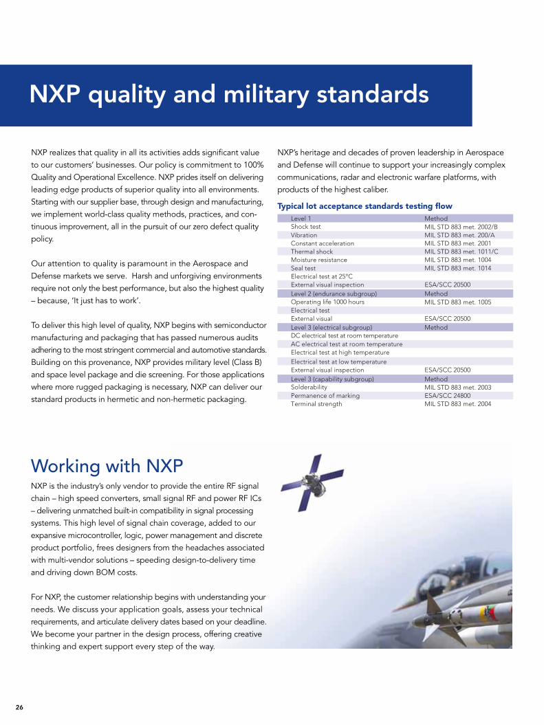
26
NXP realizes that quality in all its activities adds significant value to our customers’ businesses. Our policy is commitment to 100% Quality and Operational Excellence. NXP prides itself on delivering leading edge products of superior quality into all environments. Starting with our supplier base, through design and manufacturing, we implement world-class quality methods, practices, and con-tinuous improvement, all in the pursuit of our zero defect quality policy.
Our attention to quality is paramount in the Aerospace and Defense markets we serve. Harsh and unforgiving environments require not only the best performance, but also the highest quality – because, ‘It just has to work’.
To deliver this high level of quality, NXP begins with semiconductor manufacturing and packaging that has passed numerous audits adhering to the most stringent commercial and automotive standards. Building on this provenance, NXP provides military level (Class B) and space level package and die screening. For those applications where more rugged packaging is necessary, NXP can deliver our standard products in hermetic and non-hermetic packaging.
NXP’s heritage and decades of proven leadership in Aerospace and Defense will continue to support your increasingly complex communications, radar and electronic warfare platforms, with products of the highest caliber.
NXP is the industry’s only vendor to provide the entire RF signalchain – high speed converters, small signal RF and power RF ICs – delivering unmatched built-in compatibility in signal processing systems. This high level of signal chain coverage, added to our expansive microcontroller, logic, power management and discrete product portfolio, frees designers from the headaches associated with multi-vendor solutions – speeding design-to-delivery time and driving down BOM costs.
For NXP, the customer relationship begins with understanding your needs. We discuss your application goals, assess your technical requirements, and articulate delivery dates based on your deadline. We become your partner in the design process, offering creative thinking and expert support every step of the way.
Working with NXP
NXP quality and military standards
MIL STD 883 met. 200/AMIL STD 883 met. 2001MIL STD 883 met. 1011/CMIL STD 883 met. 1004
MIL STD 883 met. 2002/BVibrationConstant accelerationThermal shockMoisture resistance
Shock test
ESA/SCC 20500
MIL STD 883 met. 1005Electrical testExternal visual
Operating life 1000 hours
MIL STD 883 met. 2004
MIL STD 883 met. 2003Permanence of marking ESA/SCC 24800Terminal strength
Solderability
AC electrical test at room temperatureElectrical test at high temperatureElectrical test at low temperatureExternal visual inspection ESA/SCC 20500
DC electrical test at room temperature
MIL STD 883 met. 1014
ESA/SCC 20500
Seal testElectrical test at 25ºCExternal visual inspection
Level 1 Method
Level 3 (electrical subgroup) Method
Level 3 (capability subgroup) Method
Level 2 (endurance subgroup) Method
Typical lot acceptance standards testing flow
NXP’s history of firsts in RF1963 - Philips diffuses first transistors and diodes on 0.75 inch wafers
1964 - Launches first RF wideband transistor with 1.5GHz max
1970 - Introduces the BFR90, 5GHz wideband transistor
1978 - Introduces the BFQ33, 14GHz wideband transistor
1989 - First to introduce output matching in common emitter basestation transistors
1992 - First to introduce highest-power broadcast bipolar devices
1996 - First to introduce the highest-performance 2GHz LDMOS
1999 - Introduces Bluetooth integrated radio in QUBiC3 BiCMOS process
2000 - NXP follows up with WLAN integrated radio in QUBiC3 BiCMOS process
2001 - First to demonstrate LDMOS-based 250W feedforward power amplifier at European Microwave Conference
2001 - First to fully qualify and introduce LDMOS power amplifier product BLA1011-200 for Pulsed Avionics applications
2001 - Introduces first integrated silicon tuner products in BiCMOS
2003 - First to introduce the ultra-linear LDMOS using Vt distribution at IMS2003
2004 - First to introduce an LDMOS-based 200W Doherty amplifier for UMTS at IMS2004
2004 - Introduces Gen5 LDMOS which becomes the industry’s most advanced process for power amplifiers
2005 - Introduces next level of BiCMOS with QUBiC4+
2006 - First to introduce fully integrated Doherty transistors
2006 - First to introduce ultra-thin leadless packages for breakthrough RF performance
2007 - Launches TFF1004HN, industry’s first fully integrated, silicon-based IC solution for satellite LNB
2007 - First to introduce high-power Novel 3-way Doherty for UMTS/LTE
2007 - NXP shows highest level of integration in BiCMOS with introduction of most advanced WiMAX transceivers
2008 - Introduces the first high-speed data converters based on JESD204A standard
2009 - First to launch 1kW single transistor (BLF578) PA for FM radio (88 to 108MHz)
2009 - First to introduce industry standard radar pallets with LDMOS transistors
2009 - First to introduce state-of-the-art next generation SiGe(C) BiCMOS QUBiC4x technology
2010 - NXP releases into production its new range of CGV™ high-speed data converters, the world’s first high-speed converters featuring the new JEDEC JESD204A serial interface standard
27
www.nxp.com
©2010 NXP B.V.All rights reserved. Reproduction in whole or in part is prohibited without the prior written consent of the copyright owner. The information presented in this document does not form part of any quotation or contract, is believed to be accurate and reliable and may be changed without notice. No liability will be accepted by the publisher for any consequence of its use. Publication thereof does not convey nor imply any license under patent- or other industrial or intellectual property rights.
Date of release: October 2010Document order number: 9397 750 17008Printed in the Netherlands