high-efficiency transformerless pv inverter circuits · high-efficiency transformerless pv inverter...
TRANSCRIPT
High-efficiency Transformerless PV Inverter
Circuits
Baifeng Chen
Dissertation submitted to the Faculty of the
Virginia Polytechnic Institute and State University
in partial fulfillment of the requirements for the degree of
Doctor of Philosophy
In
Electrical Engineering
Jih-Sheng Lai, Committee Chair
William T. Baumann
Douglas J. Nelson
Kathleen Meehan
Qiang Li
August 13, 2015
Blacksburg, Virginia
Keywords: Photovoltaic inverter, PV inverter, transformerless inverter,
MOSFET inverter, multilevel inverter, leakage current, common mode,
inverter control, reactive power generation
Copyright 2015, Baifeng Chen
High-efficiency Transformerless PV Inverter
Circuits
Baifeng Chen
ABSTRACT
With worldwide growing demand for electric energy, there has been a great
interest in exploring photovoltaic (PV) sources. For the PV generation system,
the power converter is the most essential part for the efficiency and function
performance. In recent years, there have been quite a few new transformerless
PV inverters topologies, which eliminate the traditional line frequency
transformers to achieve lower cost and higher efficiency, and maintain lower
leakage current as well.
With an overview of the state-of-the-art transformerless PV inverters, a
new inverter technology is summarized in the Chapter 2, which is named V-
NPC inverter technology. Based this V-NPC technology, a family of high
efficiency transformerless inverters are proposed and detailly analyzed. The
experimental results demonstrate the validity of V-NPC technology and high
performance of the transformerless inverters.
For the lower power level transformerless inverters, most of the innovative
topologies try to use super junction metal oxide semiconductor field effect
transistor (MOSFET) to boost efficiency, but these MOSFET based inverter
topologies suffer from one or more of these drawbacks: MOSFET failure risk
iii
from body diode reverse recovery, increased conduction losses due to more
devices, or low magnetics utilization. By splitting the conventional MOSFET
based phase leg with an optimized inductor, Chapter 3 proposes a novel
MOSFET based phase leg configuration to minimize these drawbacks. Based
on the proposed phase leg configuration, a high efficiency single-phase
MOSFET transformerless inverter is presented for the PV micro-inverter
applications. The PWM modulation and circuit operation principle are then
described. The common mode and differential mode voltage model is then
presented and analyzed for circuit design. Experimental results of a 250 W
hardware prototype are shown to demonstrate the merits of the proposed
MOSFET based phase-le and the proposed transformerless inverter.
New codes require PV inverters to provide system regulation and service to
improve the distribution system stabilization. One obvious impact on PV
inverters is that they now need to have reactive power generation capability.
The Chapter 4 improves the MOFET based transformerless inverter in the
Chapter 3 and proposed a novel pulse width modulation (PWM) method for
reactive power generation. The ground loop voltage of this inverter under the
proposed PWM method is also derived with common mode and differential
mode circuit analyses, which indicate that high-frequency voltage component
can be minimized with symmetrical design of inductors. A 250-W inverter
hardware prototype has been designed and fabricated. Steady state and
transient operating conditions are tested to demonstrate the validity of
iv
improved inverter and proposed PWM method for reactive power generation,
high efficiency of the inverter circuit, and the high-frequency-free ground loop
voltage.
Besides the high efficiency inverter circuit, the grid connection function is
also the essential part of the PV system. The Chapter 5 present the overall
function blocks for a grid-connected PV inverter system. The current control
and voltage control loop is then analyzed, modeled, and designed. The dynamic
reactive power generation is also realized in the control system. The new PLL
method for the grid frequency/voltage disturbance is also realized and
demonstrate the validity of the detection and protection capability for the
voltage/frequency disturbance.
At last, a brief conclusion is given in the Chapter 6 about each work. After
that, future works on device packaging, system integration, innovation on
inverter circuit, and standard compliance are discussed.

v
To my parents Mingbing Chen
Dimei Xu

vi
ACKNOWLEDGEMENTS
First, I would like to express my deepest gratitude and respect to my
advisor, Dr. Jih-Sheng Lai, for his professional supervision and experienced
guidance. Without his continuous support and encouragement, I could not
complete my projects and finish this Ph.D. program.
I would also like to express my sincere thanks to my advisory committee
members: Dr. William T. Baumann, Dr. Douglas J. Nelson, Dr. Kathleen
Meehan, and Dr. Qiang Li for their professional suggestions and comments
throughout my pursuit of the Ph.D. degree.
It want to thank to all the talented colleagues in the Future Energy
Electronics Center (FEEC). I would like to thank Mr. Gary Kerr, Dr. Wensong
Yu, Dr. Chien-Liang Chen, Dr. Younghoon Cho, Dr. Ethan Swint, Dr. Pengwei
Sun, Dr. Ahmed Koran, Dr. Zheng Zhao, Dr. Ben York, Dr. Zakariya Dalala,
Dr. Bin Gu, Dr. Thomas LaBella, Dr. Qingqing Ma, Dr. Cong Zheng, Ms.
Hongmei Wan, Mr. Yaxiao Qin, Mr. Zidong Liu, Ms. Hyun-Soo Koh, Mr. Zaka
Ullah Zahid, Mr. Eric Faraci, Mr. Rui Chen, Mr. Jason Dominic, Mr. Lanhua
Zhang, Ms. Xiaonan Zhao, Mr. Seung-Ryul Moon, Mr. Andrew Amrhein, Ms.
Rachael Born, Mr. Bo Zhou, Mr. Wei-Han Lai, Mr. Hidekazu Miwa, Mr. Hsin
Wang, Ms. Le Du, Mr. Chris Hutchens, Mr. Alex Kim, Mr. Nathan Kees, Mr.
Brett Whitaker, and Mr. Daniel Martin. My studies and research were
enjoyable with their friendly companionship and great support. My gratitude
also goes out to the visiting scholars and professors, Dr. Yen-Shin Lai, Dr.

vii
Chung-Yi Lin, Mr. Yuchen Liu, Dr. Chuang Liu, Dr. Bo-Yuan Chen, Dr.
Ruixiang Hao, Dr. Zhiling Liao, Dr. Deshang Sha, Dr. Xueshen Cui, Dr.
Hongbo Ma, Dr. Huang-Jen Chiu, Dr. Chien-Yu Lin, Dr. Yan Li, Dr. Chia-His
Chang, and Dr. Kuan-Hong Wu, for their help with my lab work and my life.
I want to express my deepest gratitude to my parents, Mingbing Chen and
Dimei Xu, my brother and sister in law, Hongzhou Xu and Xiaoyan Zhang, for
their substantial and continuous love, support, and encouragement with every
venture that I undertake during my life.
Baifeng Chen
07/07/2015 in Blacksburg
viii
CONTENTS
CHAPTER 1 INTRODUCTION ....................................................................... 1
1.1 RESEARCH BACKGROUND AND MOTIVATIONS ................................................ 1
1.2 STATE-OF-THE-ART PV INVERTERS ............................................................... 5
1.2.1 Microinverter ....................................................................................... 5
1.2.2 String inverter ..................................................................................... 6
1.2.3 Central inverter ................................................................................... 6
1.3 STATE-OF-THE-ART PV SYSTEM STRUCTURES ............................................... 6
1.3.1 Two-stage system with high frequency transformer and pseudo DC link ................................................................................................................ 6
1.3.2 Two-stage system with high frequency transformer and DC link bus voltage ........................................................................................................... 7
1.3.3 Two-stage system with non-isolated DC-DC and DC link bus voltage ........................................................................................................... 8
1.3.4 Single-stage system with line frequency transformer ....................... 8
1.3.5 Single-stage system without isolation transformer .......................... 9
1.4 OBJECTIVES OF THE RESEARCH PROJECT ................................................... 10
1.5 OUTLINE OF THE DISSERTATION ................................................................. 12
CHAPTER 2 TRANSFORMERLESS INVERTER CIRCUITS WITH
ADVANCED NEUTRAL POINT CLAMPING TECHNOLOGY .................... 15
2.1 INTRODUCTION .......................................................................................... 15
2.2 STATE-OF-THE-ART TRANSFORMERLESS INVERTERS ................................... 17
2.3 NEUTRAL POINT VIRTUALLY CLAMPED (V-NPC) TECHNOLOGY WITH
AUXILIARY FREEWHEELING SWITCHES ............................................................. 26
2.4 A FAMILY OF HIGH-EFFICIENCY TRANSFORMERLESS INVERTER CIRCUITS
WITH V-NPC TECHNOLOGY ............................................................................. 30
2.4.1 Proposed inverter topologies ............................................................. 31
2.4.2 PWM method and working principle ................................................ 33
2.4.3 Efficiency calculation and loss analysis ........................................... 41
2.4.4 Experimental Results ........................................................................ 47
2.5 INVERTER CIRCUITS WITH IMPROVED V-NPC TECHNOLOGY FOR HIGH INPUT
DC VOLTAGE APPLICATION ................................................................................ 52
2.5.1 Single-phase full bridge NPC inverter ............................................. 52
2.5.2 Inverter circuit with V-NPC method .............................................. 55
2.5.3 A family of inverter circuits with improved V-NPC method ........... 56
2.6 SUMMARY .................................................................................................. 59
CHAPTER 3 MOSFET BASED TRANSFORMERLESS INVERTER
CIRCUIT WITH HIGH MAGNETIC UTILIZATION ..................................... 60
3.1 INTRODUCTION .......................................................................................... 60
3.2 STATE-OF-THE-ART MOSFET BASED TRANSFORMERLESS INVERTERS ........ 61
3.2.1 Transformerless inverter with MOSFET phase-leg ........................ 61

ix
3.2.2 Transformerless inverter without MOSFET phase-leg ................... 63
3.3 PROPOSED MOSFET BASED PHASE-LEG METHOD ...................................... 65
3.4 PROPOSED TRANSFORMERLESS INVERTER WITH PROPOSED PHASE-LEG ...... 69
3.4.1 Proposed transformerless inverter circuit ........................................ 69
3.4.2 PWM method and operating modes .................................................. 70
3.4.3 Ground loop voltage analysis ............................................................ 74
3.4.4 Component selection and loss analysis ............................................ 79
3.4.5 Experimental results ......................................................................... 84
3.5 GENERAL APPLICATIONS OF PROPOSED MOSFET BASED PHASE-LEG ......... 89
3.6 SUMMARY .................................................................................................. 91
CHAPTER 4 REACTIVE POWER GENERATION ON MOSFET BASED
TRANSFORMERLESS INVERTER ............................................................... 93
4.1 INTRODUCTION .......................................................................................... 93
4.2 REACTIVE POWER CAPABILITY FOR CURRENT MOSFET BASED
TRANSFORMERLESS INVERTERS ........................................................................ 96
4.2.1 High efficiency topologies suffer from MOSFET body diode reverse recovery for reactive power generation ..................................................... 97
4.2.2 High efficiency MOSFET inverters don’t support reactive power generation ................................................................................................... 98
4.2.3 MOSFET inverter support reactive power generation .................... 99
4.2.4 A improved MOSFET inverter for reactive power generation ...... 100
4.3 OPERATING MODES OF THE IMPROVED MOSFET BASED TRANSFORMERLESS
INVERTERS ..................................................................................................... 102
4.4 PWM METHOD AND REALIZATION FOR IMPROVED MOSFET INVERTER .... 106
4.5 GROUND LOOP VOLTAGE ANALYSIS UNDER REACTIVE POWER GENERATION
...................................................................................................................... 114
4.6 EXPERIMENTAL RESULTS ......................................................................... 118
4.7 SUMMARY ................................................................................................ 124
CHAPTER 5 GRID CONNECTION ANALYSIS AND DESIGN ................. 126
5.1 INTRODUCTION ........................................................................................ 126
5.2 SYSTEM CONTROL AND MODELING ............................................................ 127
5.2.1 Current loop modeling and control ................................................. 128
5.2.2 DC voltage loop modeling and control ............................................ 136
5.3 DYNAMIC REACTIVE POWER GENERATION ................................................. 141
5.4 A NOVEL PLL FOR GRID VOLTAGE/FREQUENCY DISTURBANCE .................. 146
5.4.1 Traditional PLL method ................................................................. 146
5.4.2 Improved PLL method .................................................................... 149
5.4.3 Voltage magnitude detection method ............................................. 153
5.5 SUMMARY ................................................................................................ 156
CHAPTER 6 CONCLUSIONS AND FUTURE WORK ................................ 158
6.1 CONCLUSIONS .......................................................................................... 158
6.2 FUTURE WORK ......................................................................................... 160

x
LIST OF PUBLICATIONS ............................................................................ 162
REFERENCE ................................................................................................ 167
xi
LIST OF FIGURES
Figure 1.1 Microinverter, string inverter, and central inverter. ....................... 5
Figure 1.2 Two-stage system with high frequency transformer and pseudo DC
link. ............................................................................................................... 7
Figure 1.3 Two-stage system with high frequency transformer and DC link
bus voltage. ................................................................................................... 8
Figure 1.4 Two-stage system with non-isolated DC-DC and DC link bus
voltage. .......................................................................................................... 8
Figure 1.5 Single-stage system with line frequency transformer. .................... 9
Figure 1.6 Single-stage system without isolation transformer. ...................... 10
Figure 2.1 PV inverter system with transformer. ............................................ 15
Figure 2.2 The transformerless PV inverter system. ...................................... 16
Figure 2.3 Transformerless inverter system with parasitic capacitance. ....... 16
Figure 2.4 Neutral point clamp (NPC) inverter .............................................. 18
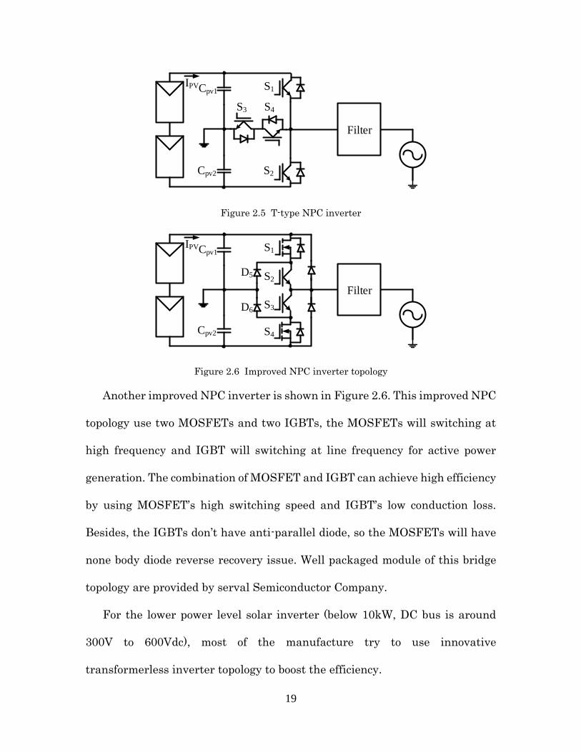
Figure 2.5 T-type NPC inverter ....................................................................... 19
Figure 2.6 Improved NPC inverter topology ................................................... 19
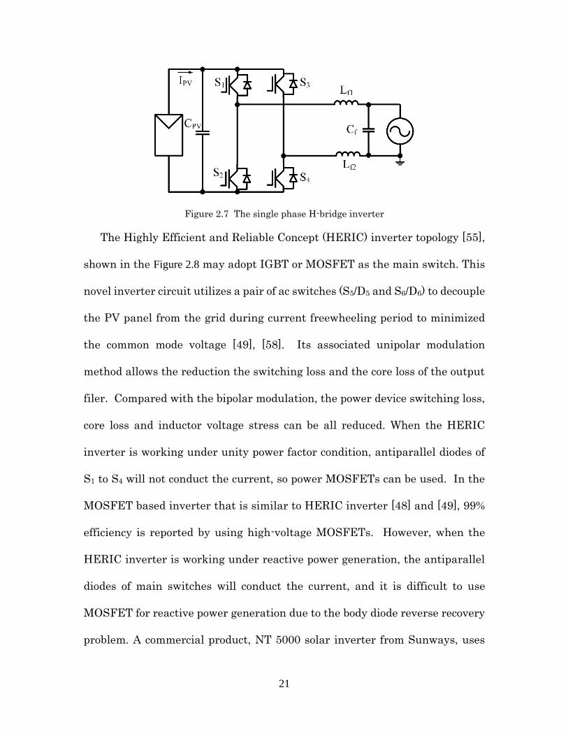
Figure 2.7 The single phase H-bridge inverter ............................................... 21
Figure 2.8 The HERIC inverter with paralleled auxiliary freewheeling
switches ...................................................................................................... 22
Figure 2.9 The HERIC inverter topology with back-to-back auxiliary
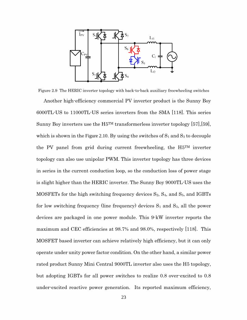
freewheeling switches ................................................................................ 23
Figure 2.10 The H5TM inverter topology .......................................................... 24
Figure 2.11 The H6 inverter topology ............................................................. 25
Figure 2.12 The symmetrical H6 inverter topology ........................................ 25
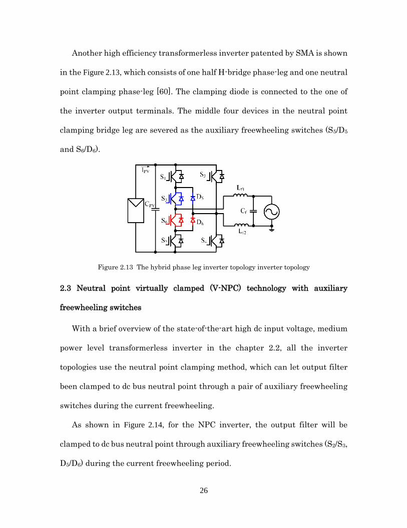
Figure 2.13 The hybrid phase leg inverter topology inverter topology .......... 26
Figure 2.14 Current freewheeling path for NPC inverter .............................. 27
Figure 2.15 Current freewheeling path for T-type inverter ........................... 27
Figure 2.16 Current freewheeling path of HERIC inverter ........................... 28
Figure 2.17 Current freewheeling path of H6 inverter .................................. 28
Figure 2.18 Current freewheeling path of H5 inverter .................................. 29
Figure 2.19 Current freewheeling path of symmetrical H6 inverter ............. 29
Figure 2.20 Current freewheeling path of the hybrid phase leg inverter ...... 30
Figure 2.21 Proposed a family of transformerless inverters .......................... 33
Figure 2.22 PWM implemented circuit for the proposed inverter ................. 34
Figure 2.23 The unipolar modulation gating signals for proposed inverter .. 34
Figure 2.24 Operating modes of the proposed transformerless inverter
Topology 1 in Figure 2.21(a): (a) Positive half-line cycle, S1 and S4 are on,
(b) Positive half-line cycle, S1 and S4 are off, free-wheeling current goes
through S5 and S6, (c) Negative half-line cycle, S3 and S2 are on, (d)
Negative half-line cycle, S3 and S2 are off, freewheeling current goes
through S5 and S6. ...................................................................................... 36
Figure 2.25 Operating modes of the inverter 3 in Figure 2.21(c): (a) Positive
half-line cycle, S1 and S4 are on, (b) Positive half-line cycle, S1 and S4 are

xii
off, free-wheeling current goes through S5 and D5, (c) Negative half-line
cycle, S3 and S2 are on, (d) Negative half-line cycle, S3 and S2 are off,
freewheeling current goes through D6 and S6. .......................................... 38
Figure 2.26 Simulation results of: (I) Topology 1 in Figure 2.21 (a); (II)
Topology 3 in Figure 2.21 (c) ...................................................................... 40
Figure 2.27 Calculated individual power loss under different power levels .. 47
Figure 2.28 Calculated total loss and efficiency under different power levels
..................................................................................................................... 47
Figure 2.29 250W micro-inverter hardware prototype ................................... 48
(a) 48
(b) 49
Figure 2.30 PWM gate signals waveforms for proposed inverter .................. 49
Figure 2.31 Output voltage/ current and ground loop voltage waveforms .... 49
Figure 2.32 The equivalent ground loop in proposed inverter topology 1 in
Fig. 21(a) ..................................................................................................... 49
Figure 2.33 Simulation results of ground loop voltage V_EG in proposed
inverter topology 1 in Fig. 21(a) ................................................................ 50
Figure 2.34 Calculated and test efficiency results under different power
levels ........................................................................................................... 51
Figure 2.35 The half bridge NPC inverter. ..................................................... 52
Figure 2.36 The single-phase full bridge NPC inverter. ................................. 53
Figure 2.37 The PWM implementation method and gating signals for single-
phase full bridge NPC inverter. ................................................................. 53
Figure 2.38 Operating modes of single-phase full bridge NPC inverter ........ 54
Figure 2.39 NPC single-phase full bridge inverter with V-NPC method ...... 55
Figure 2.40 Operating modes of V-NPC based single-phase full bridge
inverter ....................................................................................................... 55
Figure 2.41 A family of single-phase full bridge inverters based on improved
V-NPC technology ...................................................................................... 57
Figure 2.42 The output voltage, output current, and drain source voltage of
devices ......................................................................................................... 58
Figure 3.1 (a) Complimentary phase-leg with CoolMOS; (b) Buck converter
with CoolMOS and SiC diode. ................................................................... 61
Figure 3.2 The two stage topology with pseudo DC link ................................ 63
Figure 3.3 Dual buck transformerless inverter .............................................. 63
Figure 3.4 Bidirectional dual buck inverter .................................................... 65
Figure 3.5 MOSFET phase leg configurations: (a) Traditional phase leg, (b)
Dual buck method, (c) Proposed method. .................................................. 65
Figure 3.6 Double pulse test of the body diode reverse recovery ................... 67
Figure 3.7 Diode reverse recovery of IPB60R099C6 in (a) traditional phase
leg (b) proposed phase leg. ......................................................................... 68
Figure 3.8 Proposed transformerless inverter topology with (a) separated
magnetics (b) integrated magnetics .......................................................... 69
Figure 3.9 PWM implemented circuit for the proposed inverter. .................. 71

xiii
Figure 3.10 PWM signals in time domain for the proposed inverter. ............ 71
Figure 3.11 Operating modes of the proposed transformerless inverter: (a)
Positive half-line cycle, S1 and S4 are on, (b) Positive half-line cycle, S1
and S4 are off, free-wheeling current goes through S5 and D5, (c) Negative
half-line cycle, S3 and S2 are on, (d) Negative half-line cycle, S3 and S2 are
off, free-wheeling current goes through S6 and D6.................................... 73
Figure 3.12 The inverter system with ground loop parasitic capacitor ......... 75
Figure 3.13 Equivalent circuit with CM and DM model for the positive half-
line cycle ..................................................................................................... 75
Figure 3.14 Equivalent circuit with CM and DM model for the negative half-
line cycle ..................................................................................................... 77
Figure 3.15 Calculated individual power loss under different power levels. . 84
Figure 3.16 Calculated total loss and efficiency under different power levels.
..................................................................................................................... 84
Figure 3.17 250W two stage non-isolated micro-inverter hardware prototype.
..................................................................................................................... 85
Figure 3.18 Output voltage and current waveforms. ...................................... 86
Figure 3.19 PWM gate signals waveforms. ..................................................... 86
Figure 3.20 Inverter splitting inductor current waveform. ............................ 87
Figure 3.21 Waveforms of Voltage between grid ground and DC ground (VEG)
..................................................................................................................... 87
Figure 3.22 Efficiency test results of 250W proposed inverter. ..................... 88
(a)NPC topology (b) NPC topology with proposed phase-leg ....... 89
Figure 3.23 Application of proposed MOSFET phase-leg on NPC topology .. 89
(a) T-type inverter topology (b) T-type inverter topology with proposed
phase-leg ..................................................................................................... 90
Figure 3.24 Application of proposed MOSFET phase-leg on T-type inverter 90
(a) H-bridge topology (b) H-bridge topology with proposed phase-
leg ................................................................................................................ 90
Figure 3.25 Application of proposed MOSFET phase-leg on H-bridge topology
..................................................................................................................... 90
(a) H5 topology (b) H5 topology with proposed phase-leg .......... 90
Figure 3.26 Application of proposed MOSFET phase-leg on H5 topology ..... 90
(a) H6 topology (b) H6 topology with proposed phase-leg .......... 91
Figure 3.27 Application of proposed MOSFET phase-leg on H6 topology ..... 91
(a) Asymmetry H6 topology (b) Asymmetry H6 topology with
proposed phase-leg ..................................................................................... 91
Figure 3.28 Application of proposed MOSFET phase-leg on asymmetry H6
topology ....................................................................................................... 91
Figure 4.1 Power line voltage distribution in PV generation system
with/without reaction power compensation of PV inverters. ................... 93
Figure 4.2 Four different regions in time domain under current lagging
condition ..................................................................................................... 95
xiv
Figure 4.3 MOSFET phase leg configurations: (a) Traditional phase-leg
method, (b) unidirectional buck method, (c) Bidirectional buck method. 97
Figure 4.4 High efficiency transformerless inverter suffer MOSFET body
diode reverse recovery for reactive power generation .............................. 98
Figure 4.5 High efficiency transformerless inverter don’t support reactive
power generation ........................................................................................ 99
Figure 4.6 MOSFET based inverter support reactive power generation ..... 100
Figure 4.7 MOSFET based Phase-leg method .............................................. 101
Figure 4.8 Improved CoolMOS/SiC-diode based transformerless inverter.. 101
Figure 4.9 Buck operating mode in the I region ........................................... 103
Figure 4.10 Boost operating mode in the II region ....................................... 104
Figure 4.11 Buck operating mode in the III region ...................................... 105
Figure 4.12 Boost operating mode in the IV region ...................................... 105
Figure 4.13 Control system for voltage reference generation ...................... 107
Figure 4.14 Individual duty cycle generation and PWM modulation method
................................................................................................................... 107
Figure 4.15 Corresponding codes in DSP for duty cycle generator modules109
Figure 4.16 Gating signals of S1/ S4, S5, S2/ S3, and S6 for unity power factor
condition ................................................................................................... 111
Figure 4.17 Gating signals of S1/ S4, S5, S2/ S3, and S6 for current leading
condition ................................................................................................... 112
Figure 4.18 Gating signals of S1/ S4, S5, S2/ S3, and S6 for current lagging
condition. .................................................................................................. 113
Figure 4.19 The inverter system with ground loop parasitic capacitor ....... 114
Figure 4.20 Equivalent circuit with CM and DM model in region II ........... 115
Figure 4.21 Equivalent circuit with CM and DM model in region IV .......... 116
Figure 4.22 250W micro-inverter hardware prototype ................................. 118
Figure 4.23 The PWM gating signals for unity power factor (PF=1) operation
................................................................................................................... 119
Figure 4.24 The PWM gating signals for current leading (PF=-0.7) operation
................................................................................................................... 119
Figure 4.25 The PWM gating signals for current lagging (PF=0.7) operation
................................................................................................................... 120
Figure 4.26 Voltage and current under PF=1 ............................................... 121
Figure 4.27 Voltage and current under PF=0.7 ............................................ 122
Figure 4.28 Voltage and current under PF=-0.7 ........................................... 122
Figure 4.29 Ground loop leakage current waveform .................................... 123
Figure 4.30 Efficiency test results of proposed transformless inverter ........ 124
Figure 5.1 Block diagram of a typical grid-connected inverter system ......... 126
Figure 5.2 Block diagram of a simplified control system .............................. 127
Figure 5.3 Simplified current control system ............................................... 128
Figure 5.4 Bode diagram of second-order low-pass filter ............................ 129
Figure 5.5 Bode diagram of the (s)idG ........................................................... 130
Figure 5.6 Bode diagram of the (s)mF ........................................................... 131
xv
Figure 5.8 Bode diagram of current control loop plant _( )open diG s ................ 133
Figure 5.9 Bode diagram of current controller _( )c iG s ................................. 134
Figure 5.10 Bode diagram of current control open loop_
( )open iiG s .................. 134
Figure 5.11 Bode diagram of current control close loop close_
( )iiG s ................. 135
Figure 5.13 Bode diagram of voltage loop plant _
( )open ivG s .......................... 137
Figure 5.14 Nyquist plot of voltage loop plant _
( )open ivG s ............................. 138
Figure 5.15 Bode diagram of voltage control open loop _
( )open vvG s ............... 139
Figure 5.16 Nyquist plot of voltage control open loop _( )open vvG s for wide
frequency range ........................................................................................ 139
Figure 5.17 Nyquist plot of voltage control open loop _( )open vvG s for low
frequency range ........................................................................................ 140
Figure 5.18 DC bus voltage is control from 370 to 400 Vdc ......................... 141
Figure 5.19 the steady state waveform for ac current/voltage and dc voltage
................................................................................................................... 141
Figure 5.20 Voltage-Var control with dead-band method ........................... 143
Figure 5.21 Voltage-Var control with hysteresis method ............................ 143
Figure 5.22 System block diagram of Voltage-Var control .......................... 144
Figure 5.23 Transient form unity power factor (PF=1) operation to reactive
power generation (PF=0.7) operation ...................................................... 145
Figure 5.24 Transient form unity power factor (PF=1) operation to reactive
power absorbing (PF=-0.7) operation ...................................................... 146
Figure 5.25 Block diagram of the traditional PLL module. ......................... 147
Figure 5.26 Simulation results of traditional PLL method. ........................ 148
Figure 5.27 Frequency detection results of traditional PLL. ...................... 148
Figure 5.28 Block diagram of the improved PLL module. ........................... 149
Figure 5.29 The block diagram of notch filter .............................................. 150
Figure 5.30 Frequency detection results of improved PLL. ........................ 150
Figure 5.31 Experimental abnormal over-frequency trip. ........................... 151
Figure 5.32 Experimental abnormal under-frequency trip. ........................ 151
Figure 5.33 Abnormal over-frequency test ................................................... 152
Figure 5.34 Abnormal under-frequency test ................................................ 152
Figure 5.35 Voltage magnitude detection method ....................................... 153
Figure 5.36 Under-voltage (88%) test result. ................................................ 154
Figure 5.37 Under-voltage (50%) test result. ................................................ 154
Figure 5.38 Over-voltage (110%) test result. ............................................... 155
Figure 5.39 Over-voltage (120%) test result. ............................................... 155

xvi
LIST OF TABLES
Table 5-1 Summary of abnormal frequency test results ............................... 153
Table 5-2 Summary of abnormal voltage test results ................................... 156

1
Chapter 1 Introduction
1.1 Research background and motivations
Solar energy offers a number of strategic benefits to all the world. Replacing
fossil-fuel combustion with solar energy reduces emissions of human-induced
greenhouse gases (GHGs) and air pollutants. Sunlight is a free resource, thus,
once solar technologies are installed, they have very low operating costs and
require minimal non-solar inputs—this provides insurance against
conventional fuel supply disruptions and price volatility. In addition, growing
the domestic solar energy industry could establish the solar-related industry,
and support a growing number of solar-related jobs [1].
Despite these benefits, solar energy currently supplies only a small fraction
of U.S. energy needs. The SunShot Initiative, Launched in 2011 by U.S.
Department of Energy (DOE), is aiming at paving the way for rapid, large-
scale adoption of solar electricity across the United States through research
and development (R&D) and partly through U.S. and global solar market
stimulation. The target is using solar energy to satisfy roughly 14% of U.S.
electricity demand by 2030 and 27% by 2050 [1-4].
A typical solar power generation system feature three components: balance-
of-systems that support all the system, PV modules that consist of multiple PV
cells, and power electronic converter that connect the PV cells to the power
grid.

2
Balance-of-systems include support structures, mounting hardware,
wiring, monitoring equipment, shipping, and lands. Balance-of-systems also
include system design and engineering, customer and site acquisition,
installation, permitting, interconnection and inspection, financing,
contracting, market-regulatory barriers, and operation and
maintenance[5],[6].
PV modules consist of interconnected PV cells which are fabricated from
semiconductor materials and can converter sunlight into electricity based on
the photoelectric effect. Crystalline silicon based PV modules, which can be
divided as monocrystalline and multicrystalline silicon technology, constitute
about 85% of the current PV market. The rated DC efficiencies of standard
crystalline silicon PV modules are about 14%–16%. A number of non-standard
cell architectures—such as back-contact cells—are growing because they offer
the potential for significantly higher efficiency. Thin-film PV cells, which made
from a few microns thickness bandgap semiconductor, have the benefit of low
cost and low volume due to thickness is 100 times thinner than crystalline
silicon cells. Thin-film modules have lower DC efficiencies than crystalline
silicon modules: about 9%–12% for cadmium telluride (CdTe), 6%–9% for
amorphous silicon (a-Si), and 8%–14% for alloys of copper indium gallium
diselenide (CIGS). CdTe-based thin-film modules has experienced significantly
higher maker growth during the last decade due to lower-cost and non-vacuum
characteristics. Glass is a common substrate/superstrate, but thin films can
3
also be deposited on flexible substrates/superstrates such as metal, which
allows for the potential for flexible lightweight solar modules. Eliminating the
need for glass through the use of “ultra-barrier” flexible glass replacement
materials is an important next step in thin film development [1-6].
Power electronic converter is the heart of every PV plant, which is an
environmentally power generation system that uses the PV cells to convert
sunlight into electrical power. The main task of a PV inverter is to convert
direct current into alternating current to fit with the public power distribution
grids. As there is a bottleneck for the PV cell energy conversion efficiency, PV
inverters is required to have high efficiency for the maximum solar energy
utilization. High efficiency is also required by PV inverter system’s reliable
operation, PV plants are designed to operate for at least twenty years, so
failure possibility from thermal can be reduced with high efficiency power
conversion. High efficiency is also required by PV inverter system for the low
cost and low volume design, high efficiency and high switching frequency
power electronics system can reduce the passive component and cooling
component. For custom, high efficiency PV inverter means more PV power
generation and fast return of capital investment [7-13].
Besides the high efficiency performance of PV power electronics system, the
advanced functions is also the key of all the PV plant. The PV inverter need
collect data on the energy yields of the PV plant, monitors the electrical activity
of the PV array and signals, and also need monitor the power distribution grid.

4
If the grid voltage and frequencies overcome the specified limiting, PV inverter
will disconnect from the grid to ensure safety. However, if there is a slight
disturbance in the frequency or voltage, the PV inverter will adjust its output
active or reactive power to alleviate grid management. So, advance monitor
and control technologies are needed for these PV functions [5-10].
For the PV inverters, high efficiency power electronics system and
advanced functions capability are two essential future research and
development targets. These two are also linked together, one improvement in
one aspect will influence another aspect’s performance. Besides, the PV cells
new improvement and power grid new requirement will also influence the
overall PV inverter design and function definition.
My research work is supported by DOE Sunshot Project: Field Verification
of High-Penetration Levels of PV into the Distribution Grid with Advanced
Power Conditioning Systems. The main objective of this project is to verify and
demonstrate existing and new solar power conditioning systems in the
distribution grid while emphasizing current technological issues.
Improvements are focused on high efficiency power electronics technologies,
cost effectiveness power conversion system, and power system interactions
functions [1].

5
1.2 State-of-the-art PV inverters
As shown in Figure 1.1, from the power level and application point view, solar
conversion system can be divided into microinverter system, string inverter
system, and central inverter system [14-21].
Figure 1.1 Microinverter, string inverter, and central inverter.
1.2.1 Microinverter
The power level of microinverter is usually less than 1 kW, which means it
is only designed for one PV panel, so the Maximum power point tracking
(MPPT) can be executed on panel level [14-18]. The main purpose of
microinverter is for residential application. The overall system efficiency is
around 96.5%, and all the commercial products on the market don’t have
reactive power capability [110-114].
6
1.2.2 String inverter
The power level of string inverter is usually between 1 kW and 30 kW, and
connected to one or few string of PV panels, so the MPPT can be executed on
string level [18-21]. The main purpose of string inverter is for both the
residential and commercial application. The overall system efficiency is around
97%, some commercial products can achieve around 98% high efficiency. Most
commercial string inverter products don’t support reactive power generation
[116-121].
1.2.3 Central inverter
The power level of central inverter is usually more than 30kW, some can be
several MW. One central inverter is connected a PV panel array, so the MPPT
can be only executed on PV array level [18-21]. The central inverter is specially
designed for PV plant. The overall system efficiency is around 97.5%, and all
the central inverters are required to have reactive power generation capability
[122].
1.3 State-of-the-art PV system structures
From the solar power conditioning system structure point view, the PV
inverter system can be divided into five different structure.
1.3.1 Two-stage system with high frequency transformer and pseudo DC link
The two-stage PV system with high frequency transformer and pseudo DC
link is show in Figure 1.2. The principle of this system is that: first dc to ac stage
will generate a rectified sinusoidal waveform (pseudo DC link), an unfolding
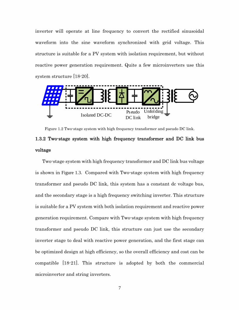
7
inverter will operate at line frequency to convert the rectified sinusoidal
waveform into the sine waveform synchronized with grid voltage. This
structure is suitable for a PV system with isolation requirement, but without
reactive power generation requirement. Quite a few microinverters use this
system structure [18-20].
Isolated DC-DCPseudo
DC link
Unfolding
bridge
Figure 1.2 Two-stage system with high frequency transformer and pseudo DC link.
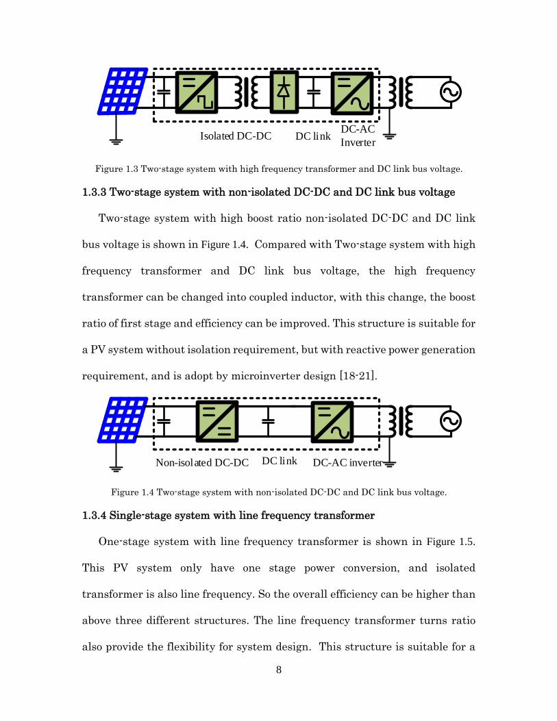
1.3.2 Two-stage system with high frequency transformer and DC link bus
voltage
Two-stage system with high frequency transformer and DC link bus voltage
is shown in Figure 1.3. Compared with Two-stage system with high frequency
transformer and pseudo DC link, this system has a constant dc voltage bus,
and the secondary stage is a high frequency switching inverter. This structure
is suitable for a PV system with both isolation requirement and reactive power
generation requirement. Compare with Two-stage system with high frequency
transformer and pseudo DC link, this structure can just use the secondary
inverter stage to deal with reactive power generation, and the first stage can
be optimized design at high efficiency, so the overall efficiency and cost can be
compatible [18-21]. This structure is adopted by both the commercial
microinverter and string inverters.
8
Isolated DC-DC DC linkDC-AC
Inverter
Figure 1.3 Two-stage system with high frequency transformer and DC link bus voltage.
1.3.3 Two-stage system with non-isolated DC-DC and DC link bus voltage
Two-stage system with high boost ratio non-isolated DC-DC and DC link
bus voltage is shown in Figure 1.4. Compared with Two-stage system with high
frequency transformer and DC link bus voltage, the high frequency
transformer can be changed into coupled inductor, with this change, the boost
ratio of first stage and efficiency can be improved. This structure is suitable for
a PV system without isolation requirement, but with reactive power generation
requirement, and is adopt by microinverter design [18-21].
Non-isolated DC-DC DC link DC-AC inverter
Figure 1.4 Two-stage system with non-isolated DC-DC and DC link bus voltage.
1.3.4 Single-stage system with line frequency transformer
One-stage system with line frequency transformer is shown in Figure 1.5.
This PV system only have one stage power conversion, and isolated
transformer is also line frequency. So the overall efficiency can be higher than
above three different structures. The line frequency transformer turns ratio
also provide the flexibility for system design. This structure is suitable for a
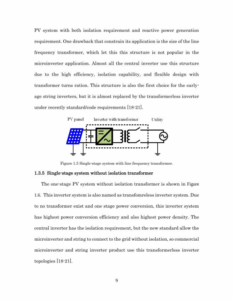
9
PV system with both isolation requirement and reactive power generation
requirement. One drawback that constrain its application is the size of the line
frequency transformer, which let this this structure is not popular in the
microinverter application. Almost all the central inverter use this structure
due to the high efficiency, isolation capability, and flexible design with
transformer turns ration. This structure is also the first choice for the early-
age string inverters, but it is almost replaced by the transformerless inverter
under recently standard/code requirements [18-21].
Figure 1.5 Single-stage system with line frequency transformer.
1.3.5 Single-stage system without isolation transformer
The one-stage PV system without isolation transformer is shown in Figure
1.6. This inverter system is also named as transfomreless inverter system. Due
to no transformer exist and one stage power conversion, this inverter system
has highest power conversion efficiency and also highest power density. The
central inverter has the isolation requirement, but the new standard allow the
microinverter and string to connect to the grid without isolation, so commercial
microinverter and string inverter product use this transformerless inverter
topologies [18-21].
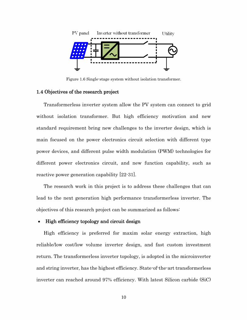
10
Figure 1.6 Single-stage system without isolation transformer.
1.4 Objectives of the research project
Transformerless inverter system allow the PV system can connect to grid
without isolation transformer. But high efficiency motivation and new
standard requirement bring new challenges to the inverter design, which is
main focused on the power electronics circuit selection with different type
power devices, and different pulse width modulation (PWM) technologies for
different power electronics circuit, and new function capability, such as
reactive power generation capability [22-31].
The research work in this project is to address these challenges that can
lead to the next generation high performance transformerless inverter. The
objectives of this research project can be summarized as follows:
High efficiency topology and circuit design
High efficiency is preferred for maxim solar energy extraction, high
reliable/low cost/low volume inverter design, and fast custom investment
return. The transformerless inverter topology, is adopted in the microinverter
and string inverter, has the highest efficiency. State-of-the-art transformerless
inverter can reached around 97% efficiency. With latest Silicon carbide (SiC)

11
devices, the efficiency have the potential to be over 98%, but suffer from higher
cost. Some special transformerless inverter topology can achieve more than
98% efficiency with cost-effective super-junction metal–oxide–semiconductor
field-effect transistors (MOSFETs), but reactive power generation capability is
suffered. So high efficiency transformerless inverter is a challenge for cost and
future standard consideration [32-60].
Common mode voltage/leakage current
Transformerless inverters don’t have isolation, but the standards has
special requirement for the ground loop leakage current. The ground loop
leakage current not only related to the common mode (CM) and differential
mode (DM) noise, but also related to the transformerless inverter circuit design
and PWM method. The detail analysis and mathematic expression of the
ground loop leakage current is one challenge for the transformerless inverter
design [62-78].
Reactive power capability with MOSFET
For traditional insulated-gate bipolar transistors (IGBTs) based PV
inverters, the reactive power generation capability is easy to realize. Recent
transformerless inverter success in adopt Super-junction MOSFET to have
higher switching frequency and higher efficiency. SiC or gallium nitride
transistors can replace IGBTs or MOSFETs for better performance, but high
cost power devices will be inconsistent with low cost PV system requirement.
But all the commercial transformerless inverter product that using MOSFET
12
can’t do reactive power generation. So MOSFETs based high efficiency
transformeless inverter with reactive power capability is one challenge for the
transformerless inverter product [79-95].
Inverter function for grid connection
Grid connection function of PV inverter is also very important, and these
advanced functions can be the heart for future PV plant. In order to stably
convert the solar power into the power grid, the system modeling and control
(current loop, voltage loop) is an essential part. If the power grid voltage or
frequency has some disturbance, the PV inverter should have fast enough
detection system to do proper response, so the system detection and control is
also an essential part [61], [96-109].
1.5 Outline of the dissertation
The present chapter provides a general overview regarding the topic of PV
inverter and discusses the research motivation behind this work. The main
objectives and major contributions of this dissertation is given. A brief
explanation of the research problems discussed in each chapter is given as
follows:
Chapter 2: High Efficiency transformerless inverter with advanced neutral
point clamping technology. This chapter begins with a brief history of
transformerlss inverter for PV application. The three-level neutral point
clamped (NPC) inverter topology is reviewed for high power PV system
application. State-of-the-art transformerless inverter topologies are
13
reviewed, a new technology is summarized, which named neutral point
virtually clamped (V-NPC) inverter technology. Based on this summarized
V-NPC technology, a family of high efficiency transformerless inverters are
proposed and verified. For the high dc input transformerless inverter
application, an improved V-NPC technology is also proposed, with the
improved V-NPC technology, a family single-phase inverter circuits is
proposed and verified.
Chapter 3: MOSFET based transformerless inverter with high magnetic
utilization. Through a brief overview of MOSFET based high efficiency
transformerless inverters, a novel MOSFET based phase leg is proposed in
this chapter. Proposed MOSFET based phase leg not only can avoid
MOSFET body diode reverse recovery issues, can achieve high magnetic
utilization, but also can be used in almost all the transformerless inverter
topologies to replace IGBTs to have higher efficiency. With proposed novel
MOSFET based phase-leg method, a high efficiency MOSFET based
tranformerless inverter is presented, circuit analysis and hardware
prototype will demonstrate the proposed inverter topology. The general
application of this proposed MOSFET based phase-leg is also
demonstrated in different inverter topologies.
Chapter 4: Reactive power generation on MOSFET based transformerless
inverter. This chapter will introduce the reactive power generation of PV
inverter. These upcoming standards will require all the PV inverters to

14
have reactive power capability. The state-of-the-art MOSFET based
transformerless inverter don’t have reactive power capability. The high
efficiency MOSFET based transformerless inverter proposed in chapter 3
has the capability for reactive power generation. This chapter will mainly
focus on how to improve the inverter circuit, how to generate proper PWM
for reactive power generation, and how to design the system component to
minimize the low common mode voltage.
Chapter 5: Grid Connection Analysis and Design. This chapter will focus
on the modeling, control, and system design for grid-connection functions.
The current loop and voltage loop is modeled for the grid connection
system. The dynamic reactive power generation, the grid information
detection with improved method is also present in this chapter for fast
dynamic response.
Chapter 6: Conclusions and Future Work. This chapter summarizes the
outcomes of the work presented in this research project and concludes the
thesis. Based on the experimental results, recommendations for future
work are also presented.
15
Chapter 2 Transformerless Inverter Circuits with Advanced
Neutral Point Clamping Technology
2.1 Introduction
With worldwide growing demand for electric energy, there has been a great
interest in exploring photovoltaic (PV) sources. As the energy conversion key
component, PV inverter system implementation method is always being
improved for the efficiency concern and standard requirement. Since the 1984,
the Section 690.41 of National Electrical Code (NEC) required a grounded
conductor for PV inverter whrere the dc voltage is over 50V [22],[23]. With both
the dc source and the utility grid grounded, the PV inverter system needs an
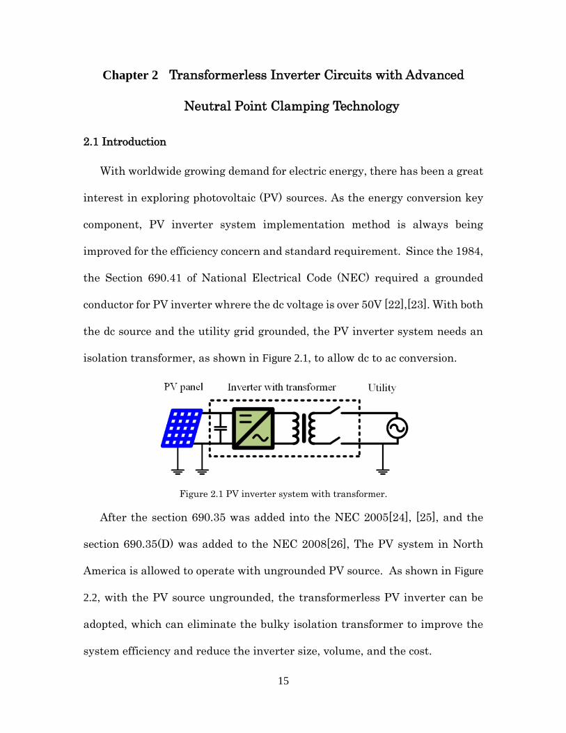
isolation transformer, as shown in Figure 2.1, to allow dc to ac conversion.
Figure 2.1 PV inverter system with transformer.
After the section 690.35 was added into the NEC 2005[24], [25], and the
section 690.35(D) was added to the NEC 2008[26], The PV system in North
America is allowed to operate with ungrounded PV source. As shown in Figure
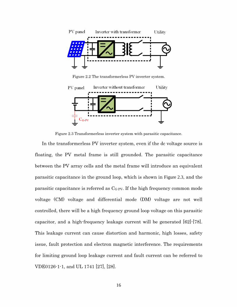
2.2, with the PV source ungrounded, the transformerless PV inverter can be
adopted, which can eliminate the bulky isolation transformer to improve the
system efficiency and reduce the inverter size, volume, and the cost.
16
Figure 2.2 The transformerless PV inverter system.
Figure 2.3 Transformerless inverter system with parasitic capacitance.
In the transformerless PV inverter system, even if the dc voltage source is
floating, the PV metal frame is still grounded. The parasitic capacitance
between the PV array cells and the metal frame will introduce an equivalent
parasitic capacitance in the ground loop, which is shown in Figure 2.3, and the
parasitic capacitance is referred as CG-PV. If the high frequency common mode
voltage (CM) voltage and differential mode (DM) voltage are not well
controlled, there will be a high frequency ground loop voltage on this parasitic
capacitor, and a high-frequency leakage current will be generated [62]-[78].
This leakage current can cause distortion and harmonic, high losses, safety
issue, fault protection and electron magnetic interference. The requirements
for limiting ground loop leakage current and fault current can be referred to
VDE0126-1-1, and UL 1741 [27], [28].
17
As discussed above, transformerless inverter can eliminated the isolation
transformer for higher efficiency, smaller volume and lower cost, but special
inverter topologies and PWM modulation methods are needed for low CM
voltage on parasitic capacitor [65]-[68]. This paper will begin with a brief
overview of the state-of-the-art single-phase transformerless inverter
topologies in chapter 2.2 3. The V-NPC technology will be summarized in the
chapter 2.3. A family of single-phase trasformreless inverters based on V-NPC
technology will be proposed in the chapter 2.4. The PWM scheme and operating
mode of proposed transformerless inverter will also be detailed in the chapter
2.4.2. Power loss analysis in the power stage and efficiency calculation will be
presented in the chapter 2.4.3. Experimental results will be shown in the
chapter 2.4.4 to verify proposed inverters. A family of inverter circuit with
improved V-NPC technology for high input dc voltage application will be
proposed in 2.5, experimental results will also be shown to demonstrate the
improved V-NPC method.
2.2 State-of-the-art transformerless inverters
In recent years, there is a considerable amount of innovations on
transformerless PV inverters [32-39], which eliminate traditional line
frequency transformers to reach lower cost and higher efficiency, and maintain
lower leakage current at the same time. The earliest and the most common one
is neutral point clamp (NPC) inverter [46],[47]. Compared with two level phase
leg, the three-level inverter has lower voltage stress devices, lower inductor
18
voltage stress. The advantage of three level not only can boost switching
frequency and efficiency to shrink the passive component and heatsink, but
also can improve control system bandwidth, EMI and audible noise.
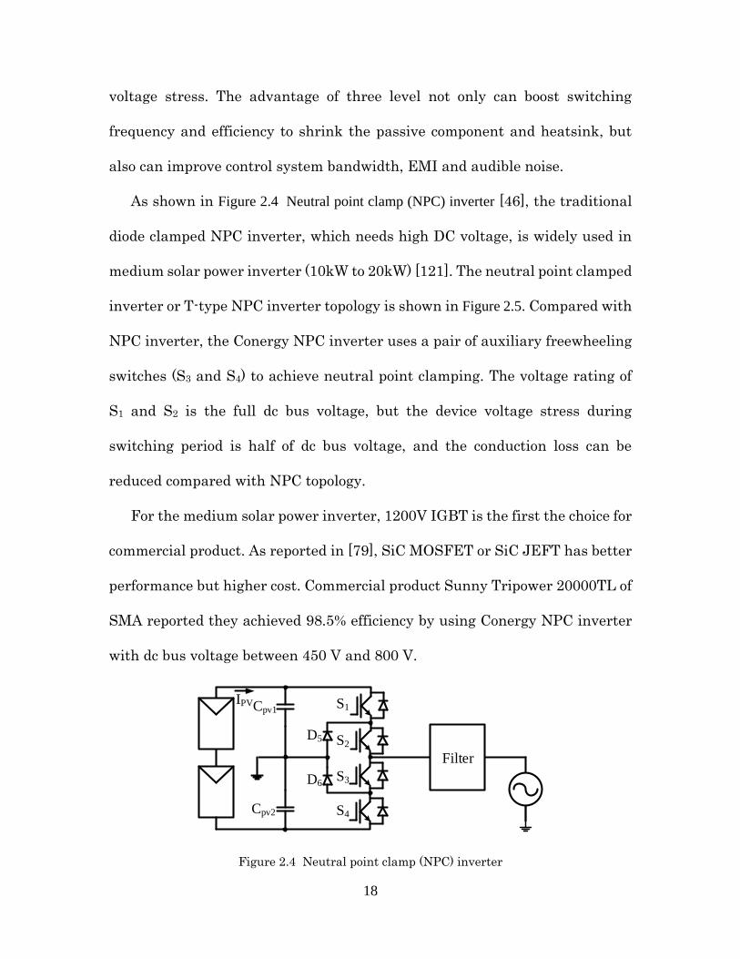
As shown in Figure 2.4 Neutral point clamp (NPC) inverter [46], the traditional
diode clamped NPC inverter, which needs high DC voltage, is widely used in
medium solar power inverter (10kW to 20kW) [121]. The neutral point clamped
inverter or T-type NPC inverter topology is shown in Figure 2.5. Compared with
NPC inverter, the Conergy NPC inverter uses a pair of auxiliary freewheeling
switches (S3 and S4) to achieve neutral point clamping. The voltage rating of
S1 and S2 is the full dc bus voltage, but the device voltage stress during
switching period is half of dc bus voltage, and the conduction loss can be
reduced compared with NPC topology.
For the medium solar power inverter, 1200V IGBT is the first the choice for
commercial product. As reported in [79], SiC MOSFET or SiC JEFT has better
performance but higher cost. Commercial product Sunny Tripower 20000TL of
SMA reported they achieved 98.5% efficiency by using Conergy NPC inverter
with dc bus voltage between 450 V and 800 V.
S1
S2
S3
S4
D5
D6
IPVCpv1
Cpv2
Filter
Figure 2.4 Neutral point clamp (NPC) inverter
19
S1
S2
S3 S4
IPVCpv1
Cpv2
Filter
Figure 2.5 T-type NPC inverter
S1
S2
S3
S4
D5
D6
IPVCpv1
Cpv2
Filter
Figure 2.6 Improved NPC inverter topology
Another improved NPC inverter is shown in Figure 2.6. This improved NPC
topology use two MOSFETs and two IGBTs, the MOSFETs will switching at
high frequency and IGBT will switching at line frequency for active power
generation. The combination of MOSFET and IGBT can achieve high efficiency
by using MOSFET’s high switching speed and IGBT’s low conduction loss.
Besides, the IGBTs don’t have anti-parallel diode, so the MOSFETs will have
none body diode reverse recovery issue. Well packaged module of this bridge
topology are provided by serval Semiconductor Company.
For the lower power level solar inverter (below 10kW, DC bus is around
300V to 600Vdc), most of the manufacture try to use innovative
transformerless inverter topology to boost the efficiency.

20
The simplest PV transformerless inverter topology is the H-bridge inverter,
as shown in Figure 2.7, which utilizes the insulated-gate-bipolar-transistors
(IGBTs) as the power device. The advantages of this inverter topology are its
simple structure and capability of producing reactive power. The main
drawback for this inverter design is it requires the use of bipolar PWM
modulation to avoid the common mode (CM) voltage [41]. As a result, the
efficiency suffers due to high switching loss on IGBTs, high current ripple
induced core and copper losses on the output filter inductor. The ABB’s string
inverter PVI-5000-OUTD-US adopts this IGBT based H-bridge topology. Its
maximum efficiency is 97.1%, and the California Energy Commission (CEC)
weighted efficiency is 96.5% [116]. The CEC efficiency suffers because IGBT
has a fixed voltage drop that significantly reduces the light-load efficiency and
also the low switching speed.
The metal oxide semiconductor field effect transistor (MOSFET) voltage
drop is a resistive and is preferred for maintaining high efficiency under light-
load conditions and also for fast switching speed. However, high-voltage
MOSFETs suffers from the slow reverse recovery and snappy body diode,
which not only produces high dv/dt, di/dt, and high power loss, but also creates
phase-leg shoot through risk due to reverse conducting current [84]-[89].
Therefore, high-voltage MOSFETs are not suitable for this H-bridge topology.
21
Figure 2.7 The single phase H-bridge inverter
The Highly Efficient and Reliable Concept (HERIC) inverter topology [55],
shown in the Figure 2.8 may adopt IGBT or MOSFET as the main switch. This
novel inverter circuit utilizes a pair of ac switches (S5/D5 and S6/D6) to decouple
the PV panel from the grid during current freewheeling period to minimized
the common mode voltage [49], [58]. Its associated unipolar modulation
method allows the reduction the switching loss and the core loss of the output
filer. Compared with the bipolar modulation, the power device switching loss,
core loss and inductor voltage stress can be all reduced. When the HERIC
inverter is working under unity power factor condition, antiparallel diodes of
S1 to S4 will not conduct the current, so power MOSFETs can be used. In the
MOSFET based inverter that is similar to HERIC inverter [48] and [49], 99%
efficiency is reported by using high-voltage MOSFETs. However, when the
HERIC inverter is working under reactive power generation, the antiparallel
diodes of main switches will conduct the current, and it is difficult to use
MOSFET for reactive power generation due to the body diode reverse recovery
problem. A commercial product, NT 5000 solar inverter from Sunways, uses
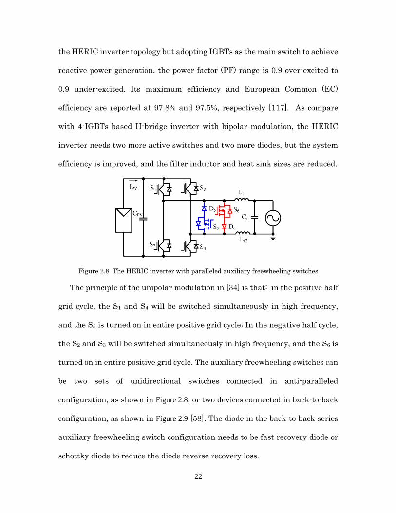
22
the HERIC inverter topology but adopting IGBTs as the main switch to achieve
reactive power generation, the power factor (PF) range is 0.9 over-excited to
0.9 under-excited. Its maximum efficiency and European Common (EC)
efficiency are reported at 97.8% and 97.5%, respectively [117]. As compare
with 4-IGBTs based H-bridge inverter with bipolar modulation, the HERIC
inverter needs two more active switches and two more diodes, but the system
efficiency is improved, and the filter inductor and heat sink sizes are reduced.
Figure 2.8 The HERIC inverter with paralleled auxiliary freewheeling switches
The principle of the unipolar modulation in [34] is that: in the positive half
grid cycle, the S1 and S4 will be switched simultaneously in high frequency,
and the S5 is turned on in entire positive grid cycle; In the negative half cycle,
the S2 and S3 will be switched simultaneously in high frequency, and the S6 is
turned on in entire positive grid cycle. The auxiliary freewheeling switches can
be two sets of unidirectional switches connected in anti-paralleled
configuration, as shown in Figure 2.8, or two devices connected in back-to-back
configuration, as shown in Figure 2.9 [58]. The diode in the back-to-back series
auxiliary freewheeling switch configuration needs to be fast recovery diode or
schottky diode to reduce the diode reverse recovery loss.
23
Figure 2.9 The HERIC inverter topology with back-to-back auxiliary freewheeling switches
Another high-efficiency commercial PV inverter product is the Sunny Boy
6000TL-US to 11000TL-US series inverters from the SMA [118]. This series
Sunny Boy inverters use the H5TM transformerless inverter topology [57],[59],
which is shown in the Figure 2.10. By using the switches of S1 and S3 to decouple
the PV panel from grid during current freewheeling, the H5TM inverter
topology can also use unipolar PWM. This inverter topology has three devices
in series in the current conduction loop, so the conduction loss of power stage
is slight higher than the HERIC inverter. The Sunny Boy 9000TL-US uses the
MOSFETs for the high switching frequency devices S2, S4, and S5, and IGBTs
for low switching frequency (line frequency) devices S1 and S3, all the power
devices are packaged in one power module. This 9-kW inverter reports the
maximum and CEC efficiencies at 98.7% and 98.0%, respectively [118]. This
MOSFET based inverter can achieve relatively high efficiency, but it can only
operate under unity power factor condition. On the other hand, a similar power
rated product Sunny Mini Central 9000TL inverter also uses the H5 topology,
but adopting IGBTs for all power switches to realize 0.8 over-excited to 0.8
under-excited reactive power generation. Its reported maximum efficiency,
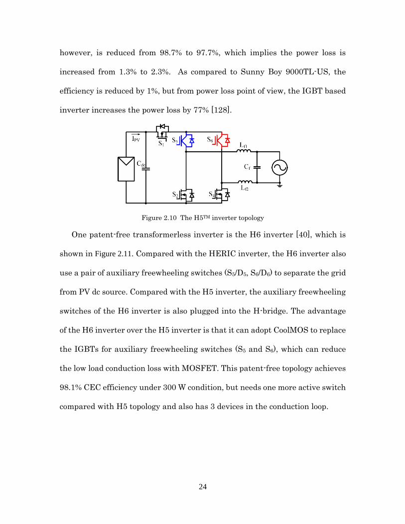
24
however, is reduced from 98.7% to 97.7%, which implies the power loss is
increased from 1.3% to 2.3%. As compared to Sunny Boy 9000TL-US, the
efficiency is reduced by 1%, but from power loss point of view, the IGBT based
inverter increases the power loss by 77% [128].
Figure 2.10 The H5TM inverter topology
One patent-free transformerless inverter is the H6 inverter [40], which is
shown in Figure 2.11. Compared with the HERIC inverter, the H6 inverter also
use a pair of auxiliary freewheeling switches (S5/D5, S6/D6) to separate the grid
from PV dc source. Compared with the H5 inverter, the auxiliary freewheeling
switches of the H6 inverter is also plugged into the H-bridge. The advantage
of the H6 inverter over the H5 inverter is that it can adopt CoolMOS to replace
the IGBTs for auxiliary freewheeling switches (S5 and S6), which can reduce
the low load conduction loss with MOSFET. This patent-free topology achieves
98.1% CEC efficiency under 300 W condition, but needs one more active switch
compared with H5 topology and also has 3 devices in the conduction loop.
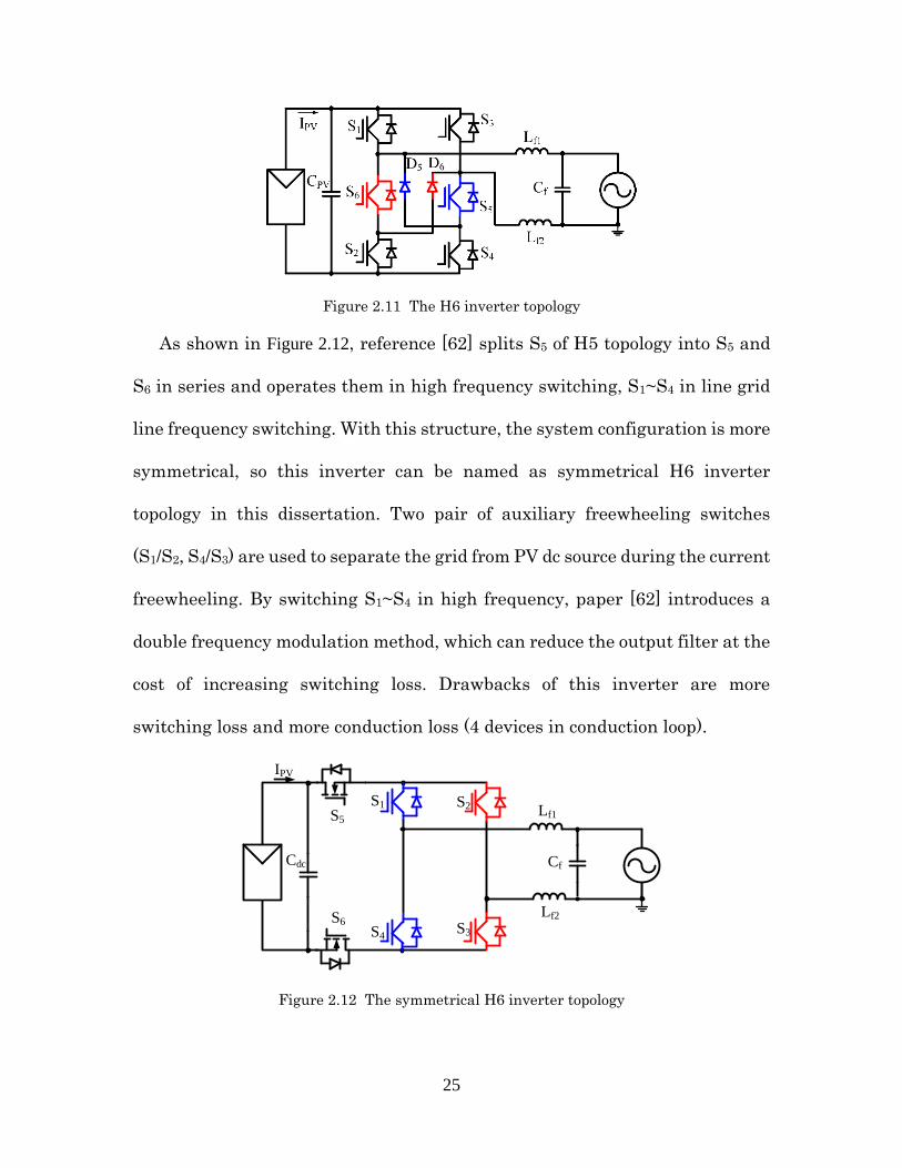
25
Figure 2.11 The H6 inverter topology
As shown in Figure 2.12, reference [62] splits S5 of H5 topology into S5 and
S6 in series and operates them in high frequency switching, S1~S4 in line grid
line frequency switching. With this structure, the system configuration is more
symmetrical, so this inverter can be named as symmetrical H6 inverter
topology in this dissertation. Two pair of auxiliary freewheeling switches
(S1/S2, S4/S3) are used to separate the grid from PV dc source during the current
freewheeling. By switching S1~S4 in high frequency, paper [62] introduces a
double frequency modulation method, which can reduce the output filter at the
cost of increasing switching loss. Drawbacks of this inverter are more
switching loss and more conduction loss (4 devices in conduction loop).
S1 S2
S4S3
IPV
Cdc
S5
S6
Cf
Lf1
Lf2
Figure 2.12 The symmetrical H6 inverter topology
26
Another high efficiency transformerless inverter patented by SMA is shown
in the Figure 2.13, which consists of one half H-bridge phase-leg and one neutral
point clamping phase-leg [60]. The clamping diode is connected to the one of
the inverter output terminals. The middle four devices in the neutral point
clamping bridge leg are severed as the auxiliary freewheeling switches (S5/D5
and S6/D6).
Figure 2.13 The hybrid phase leg inverter topology inverter topology
2.3 Neutral point virtually clamped (V-NPC) technology with auxiliary
freewheeling switches
With a brief overview of the state-of-the-art high dc input voltage, medium
power level transformerless inverter in the chapter 2.2, all the inverter
topologies use the neutral point clamping method, which can let output filter
been clamped to dc bus neutral point through a pair of auxiliary freewheeling
switches during the current freewheeling.
As shown in Figure 2.14, for the NPC inverter, the output filter will be
clamped to dc bus neutral point through auxiliary freewheeling switches (S2/S3,
D5/D6) during the current freewheeling period.
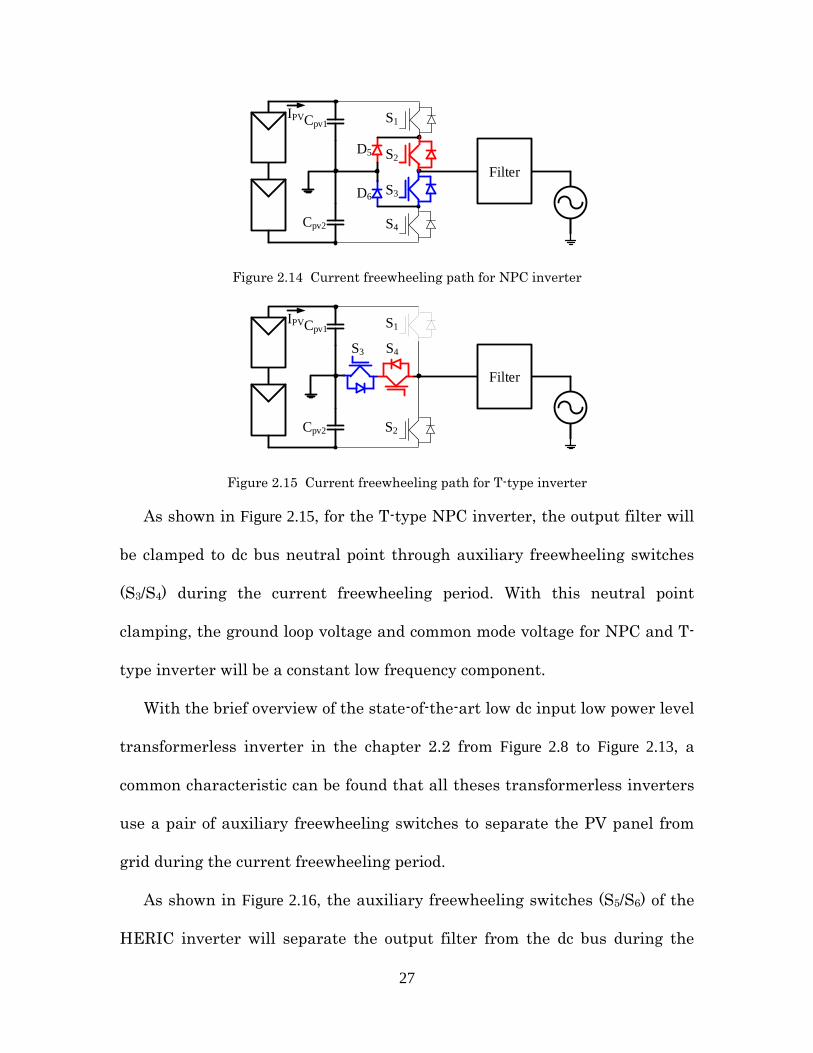
27
S1
S2
S3
S4
D5
D6
IPVCpv1
Cpv2
Filter
Figure 2.14 Current freewheeling path for NPC inverter
S1
S2
S3 S4
IPVCpv1
Cpv2
Filter
Figure 2.15 Current freewheeling path for T-type inverter
As shown in Figure 2.15, for the T-type NPC inverter, the output filter will
be clamped to dc bus neutral point through auxiliary freewheeling switches
(S3/S4) during the current freewheeling period. With this neutral point
clamping, the ground loop voltage and common mode voltage for NPC and T-
type inverter will be a constant low frequency component.
With the brief overview of the state-of-the-art low dc input low power level
transformerless inverter in the chapter 2.2 from Figure 2.8 to Figure 2.13, a
common characteristic can be found that all theses transformerless inverters
use a pair of auxiliary freewheeling switches to separate the PV panel from
grid during the current freewheeling period.
As shown in Figure 2.16, the auxiliary freewheeling switches (S5/S6) of the
HERIC inverter will separate the output filter from the dc bus during the
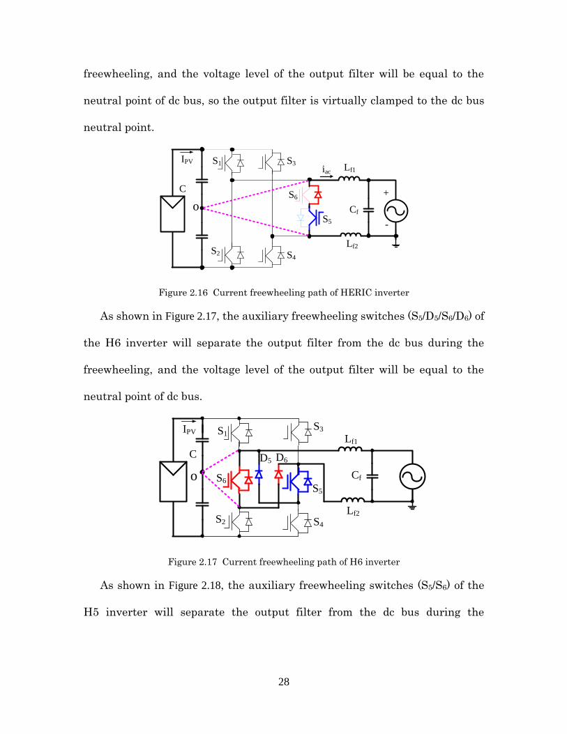
28
freewheeling, and the voltage level of the output filter will be equal to the
neutral point of dc bus, so the output filter is virtually clamped to the dc bus
neutral point.
IPV S1
S5
S6
S2 S4
S3
C
Cf
Lf1
Lf2
iac
+
-
o
Figure 2.16 Current freewheeling path of HERIC inverter
As shown in Figure 2.17, the auxiliary freewheeling switches (S5/D5/S6/D6) of
the H6 inverter will separate the output filter from the dc bus during the
freewheeling, and the voltage level of the output filter will be equal to the
neutral point of dc bus.
IPV S1
S5
S6
D5 D6
S2 S4
S3
Cf
Lf1
Lf2
o
C
Figure 2.17 Current freewheeling path of H6 inverter
As shown in Figure 2.18, the auxiliary freewheeling switches (S5/S6) of the
H5 inverter will separate the output filter from the dc bus during the
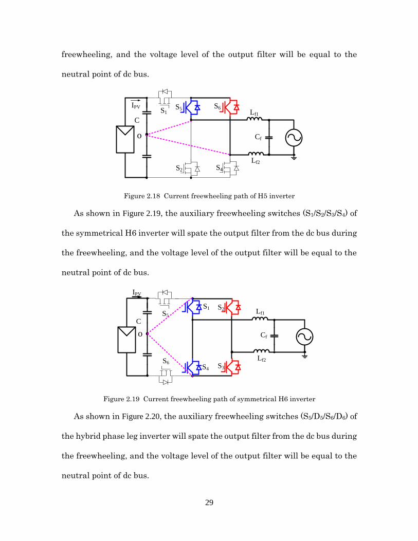
29
freewheeling, and the voltage level of the output filter will be equal to the
neutral point of dc bus.
S1S6
S2 S4
IPV S5
Cf
Lf1
Lf2
o
C
Figure 2.18 Current freewheeling path of H5 inverter
As shown in Figure 2.19, the auxiliary freewheeling switches (S1/S2/S3/S4) of
the symmetrical H6 inverter will spate the output filter from the dc bus during
the freewheeling, and the voltage level of the output filter will be equal to the
neutral point of dc bus.
S1 S2
S4S3
IPV
S5
S6
Cf
Lf1
Lf2
o
C
Figure 2.19 Current freewheeling path of symmetrical H6 inverter
As shown in Figure 2.20, the auxiliary freewheeling switches (S5/D5/S6/D6) of
the hybrid phase leg inverter will spate the output filter from the dc bus during
the freewheeling, and the voltage level of the output filter will be equal to the
neutral point of dc bus.
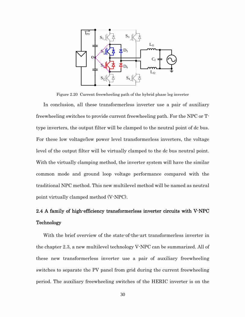
30
IPV
S1
S2 S4
S3
Cf
Lf1
Lf2
S5
S6
D5
D6
o
Figure 2.20 Current freewheeling path of the hybrid phase leg inverter
In conclusion, all these transformerless inverter use a pair of auxiliary
freewheeling switches to provide current freewheeling path. For the NPC or T-
type inverters, the output filter will be clamped to the neutral point of dc bus.
For these low voltage/low power level transformerless inverters, the voltage
level of the output filter will be virtually clamped to the dc bus neutral point.
With the virtually clamping method, the inverter system will have the similar
common mode and ground loop voltage performance compared with the
traditional NPC method. This new multilevel method will be named as neutral
point virtually clamped method (V-NPC).
2.4 A family of high-efficiency transformerless inverter circuits with V-NPC
Technology
With the brief overview of the state-of-the-art transformerless inverter in
the chapter 2.3, a new multilevel technology V-NPC can be summarized. All of
these new transformerless inverter use a pair of auxiliary freewheeling
switches to separate the PV panel from grid during the current freewheeling
period. The auxiliary freewheeling switches of the HERIC inverter is on the

31
grid side; auxiliary freewheeling switches of the H6 inverter is in the H-bridge
phase-legs, and each leg has one active switch; H5 inverter combines two
phase-leg top switches (S1 and S3) of the H6 inverter into one switch (S1); the
hybrid phase leg inverter put all the auxiliary freewheeling switches in one of
the phase-leg; the symmetrical H6 inverter use the middle H-bridge as the
auxiliary freewheeling switches.
2.4.1 Proposed inverter topologies
Based on the above overview and analysis, a new family of transformerless
single-phase inverters also based on V-NPC method are present in Figure 2.21.
The basic idea of these proposed transformerless inverters is that half of the
auxiliary freewheeling switches are put in the middle of one phase-leg, another
half auxiliary freewheeling switches are put between the two phase legs. As
shown in Figure 2.21(a), the H-bridge consists of the S1, S2, S3, and S4; the
auxiliary freewheeling switches are the S5 and S6. In this case, the S6 is put
between the phase-leg of S1 and S2, and the S5 is put between two phase-legs.
A dual circuit for the inverter circuit in Figure 2.21(a) is presented in the Figure
2.21(b). Actually, more inverter circuit can be derived with different
arrangement from Figure 2.21(a) and Figure 2.21(b). Figure 2.21(c) and Figure 2.21
(d) present similar inverter circuits with paralleled auxiliary freewheeling
switches structure (S5/D5 and S6/D6).
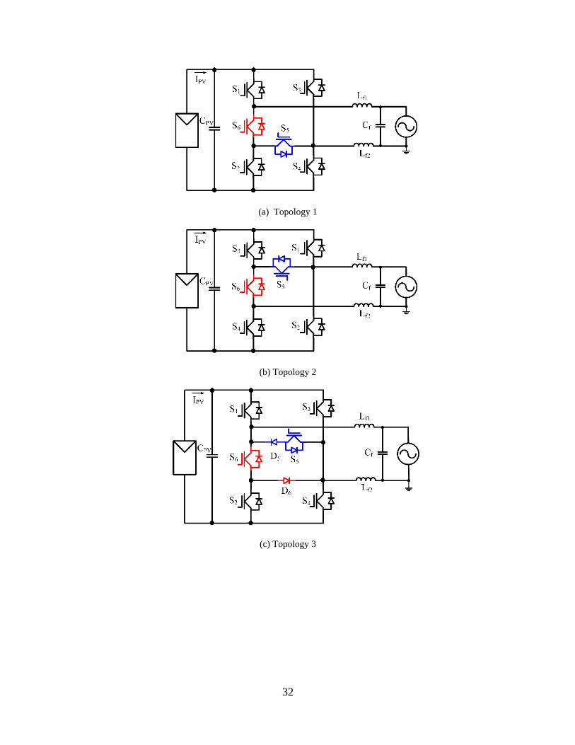
32
(a) Topology 1
(b) Topology 2
(c) Topology 3
33
(d) Topology 4
Figure 2.21 Proposed a family of transformerless inverters
2.4.2 PWM method and working principle
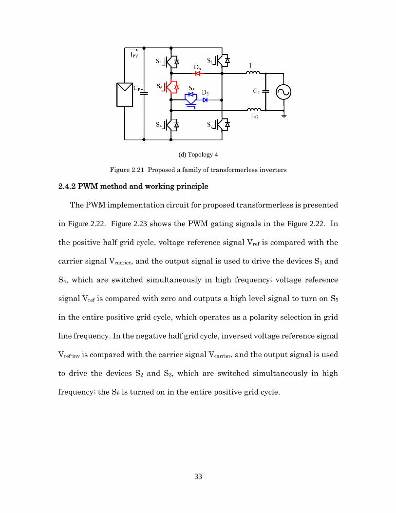
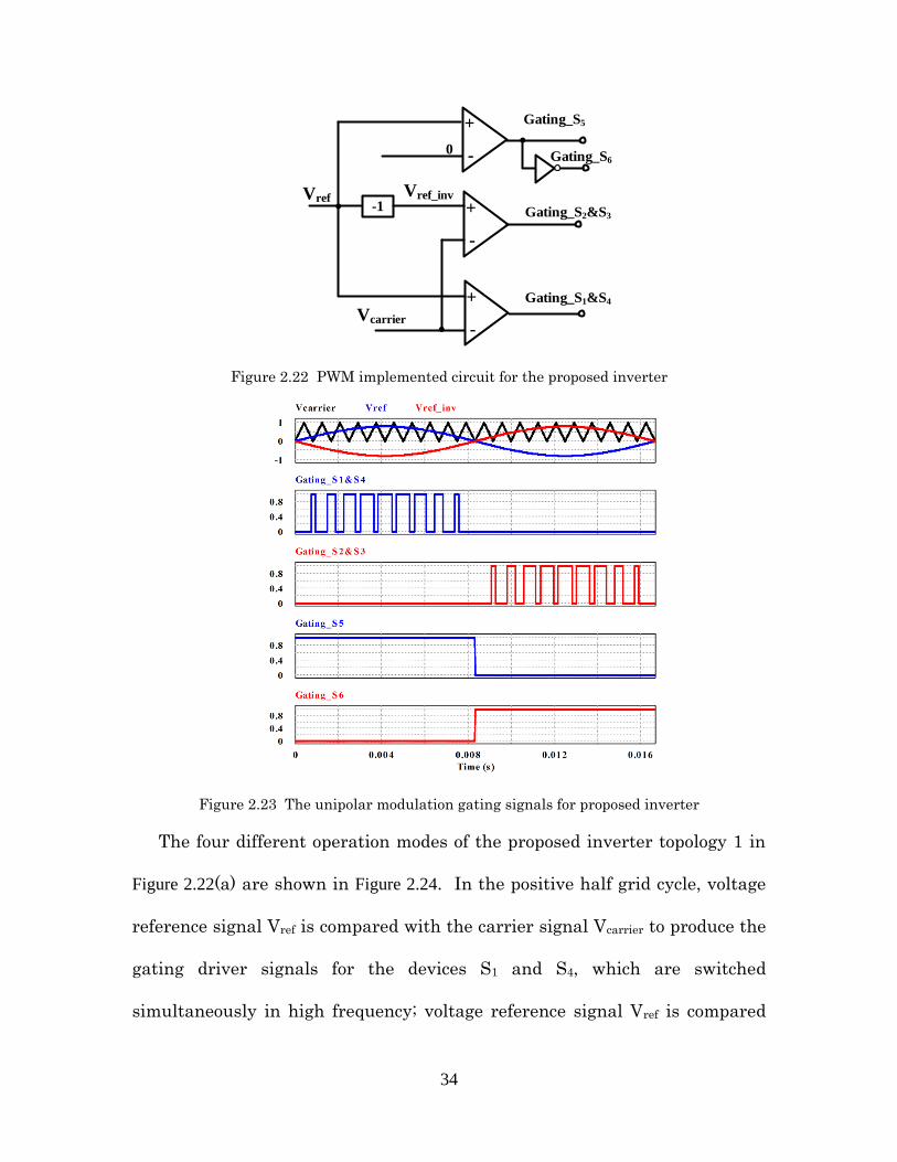
The PWM implementation circuit for proposed transformerless is presented
in Figure 2.22. Figure 2.23 shows the PWM gating signals in the Figure 2.22. In
the positive half grid cycle, voltage reference signal Vref is compared with the
carrier signal Vcarrier, and the output signal is used to drive the devices S1 and
S4, which are switched simultaneously in high frequency; voltage reference
signal Vref is compared with zero and outputs a high level signal to turn on S5
in the entire positive grid cycle, which operates as a polarity selection in grid
line frequency. In the negative half grid cycle, inversed voltage reference signal
Vref-inv is compared with the carrier signal Vcarrier, and the output signal is used
to drive the devices S2 and S3, which are switched simultaneously in high
frequency; the S6 is turned on in the entire positive grid cycle.
34
0
+
-
+
-Vcarrier
Vref-1
+
-
Gating_S1&S4
Gating_S5
Gating_S6
Gating_S2&S3
Vref_inv
Figure 2.22 PWM implemented circuit for the proposed inverter
Figure 2.23 The unipolar modulation gating signals for proposed inverter
The four different operation modes of the proposed inverter topology 1 in
Figure 2.22(a) are shown in Figure 2.24. In the positive half grid cycle, voltage
reference signal Vref is compared with the carrier signal Vcarrier to produce the
gating driver signals for the devices S1 and S4, which are switched
simultaneously in high frequency; voltage reference signal Vref is compared
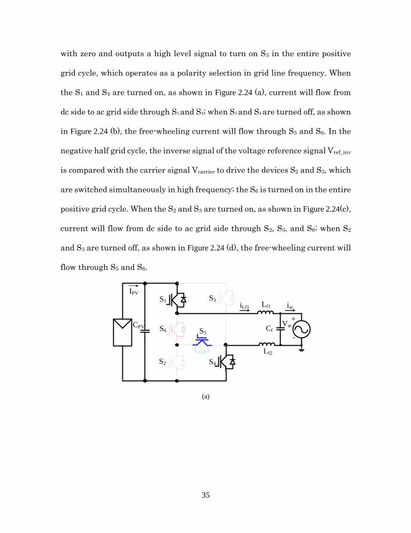
35
with zero and outputs a high level signal to turn on S5 in the entire positive
grid cycle, which operates as a polarity selection in grid line frequency. When
the S1 and S4 are turned on, as shown in Figure 2.24 (a), current will flow from
dc side to ac grid side through S1 and S4; when S1 and S4 are turned off, as shown
in Figure 2.24 (b), the free-wheeling current will flow through S5 and S6. In the
negative half grid cycle, the inverse signal of the voltage reference signal Vref_inv
is compared with the carrier signal Vcarrier to drive the devices S2 and S3, which
are switched simultaneously in high frequency; the S6 is turned on in the entire
positive grid cycle. When the S2 and S3 are turned on, as shown in Figure 2.24(c),
current will flow from dc side to ac grid side through S2, S3, and S6; when S2
and S3 are turned off, as shown in Figure 2.24 (d), the free-wheeling current will
flow through S5 and S6.
IPV
S1
S2 S4
S3
CPV Cf
Lf1
Lf2
S6 S5
iLf1
Vac+
-
iac
(a)
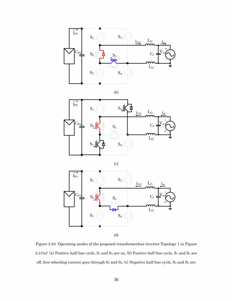
36
IPV
S1
S2 S4
S3
CPV Cf
Lf1
Lf2
S6 S5
Vac+
-
iaciLf1
(b)
IPV
S1
S2 S4
S3
CPV Cf
Lf1
Lf2
S6 S5
Vac
+
-
iaciLf1
(c)
IPV
S1
S2 S4
S3
CPV Cf
Lf1
Lf2
S6 S5
Vac
+
-
iaciLf1
(d)
Figure 2.24 Operating modes of the proposed transformerless inverter Topology 1 in Figure
2.21(a): (a) Positive half-line cycle, S1 and S4 are on, (b) Positive half-line cycle, S1 and S4 are
off, free-wheeling current goes through S5 and S6, (c) Negative half-line cycle, S3 and S2 are
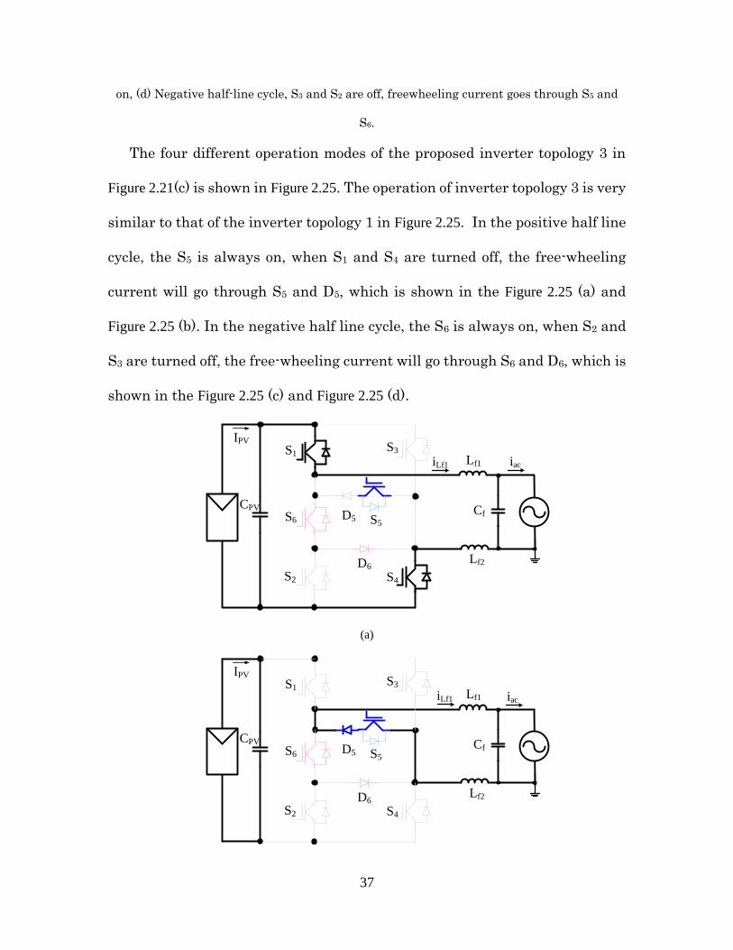
37
on, (d) Negative half-line cycle, S3 and S2 are off, freewheeling current goes through S5 and
S6.
The four different operation modes of the proposed inverter topology 3 in
Figure 2.21(c) is shown in Figure 2.25. The operation of inverter topology 3 is very
similar to that of the inverter topology 1 in Figure 2.25. In the positive half line
cycle, the S5 is always on, when S1 and S4 are turned off, the free-wheeling
current will go through S5 and D5, which is shown in the Figure 2.25 (a) and
Figure 2.25 (b). In the negative half line cycle, the S6 is always on, when S2 and
S3 are turned off, the free-wheeling current will go through S6 and D6, which is
shown in the Figure 2.25 (c) and Figure 2.25 (d).
IPV
S1
S2 S4
S3
CPV Cf
Lf1
Lf2
S6 S5D5
D6
iaciLf1
(a)
IPV
S1
S2 S4
S3
CPV Cf
Lf1
Lf2
S6 S5D5
D6
iaciLf1
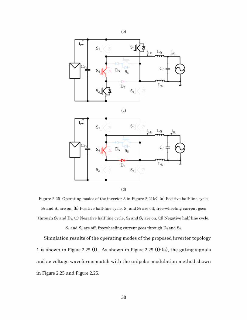
38
(b)
IPV
S1
S2 S4
S3
CPV Cf
Lf1
Lf2
S6 S5D5
D6
iaciLf1
(c)
IPV
S1
S2 S4
S3
CPV Cf
Lf1
Lf2
S6 S5D5
D6
iaciLf1
(d)
Figure 2.25 Operating modes of the inverter 3 in Figure 2.21(c): (a) Positive half-line cycle,
S1 and S4 are on, (b) Positive half-line cycle, S1 and S4 are off, free-wheeling current goes
through S5 and D5, (c) Negative half-line cycle, S3 and S2 are on, (d) Negative half-line cycle,
S3 and S2 are off, freewheeling current goes through D6 and S6.
Simulation results of the operating modes of the proposed inverter topology
1 is shown in Figure 2.25 (I). As shown in Figure 2.25 (I)-(a), the gating signals
and ac voltage waveforms match with the unipolar modulation method shown
in Figure 2.25 and Figure 2.25.

39
Detailed gating signals, voltage waveforms, and current waveforms in two
switch cycles for positive half line cycle and negative half line cycle are shown
in Figure 2.26(I)-(b) and Figure 2.26(I)-(c) respectively. In the positive half line
cycle, as shown in Figure 2.26 (I)-(b), S1 and S4 are both switching at high
frequency, S5 are always turned on, other devices are turned off, when S1 and
S4 are turned on, they will conduct the output filter inductor current iLF1; when
S1 and S4 are turned off, current will free-wheeling through the S5 and S6. In
the negative half line cycle, as shown in Figure 2.26 (I)-(c), S2 and S3 are both
switching at high frequency, S6 are always turned on, and other devices are
turned off. When S2 and S3 are turned on, the S2, S3 and S6 will conduct the
output filter inductor current iLF1; when S2 and S3 are turned off, current will
free-wheeling through the S5 and S6.
For the proposed inverter topology 3, simulation results are shown in Figure
2.26 (II). The PWM gating signals are as same as results in Figure 2.26 (I). The
difference is the current waveforms in the auxiliary freewheeling switches (S5
and S6). As shown in Figure 2.26 (II)-(b), in the positive half line cycle, when S1
and S4 are turned on, they will conduct the output filter inductor current iLF1;
when S1 and S4 are turned off, current will free-wheeling through the S5. In
the negative half line cycle, as shown in Figure 2.26 (II)-(c), when S2 and S3 are
turned on, the S2, S3 and S6 will conduct the output filter inductor current iLF1;
when S2 and S3 are turned off, current will free-wheeling through the S6.
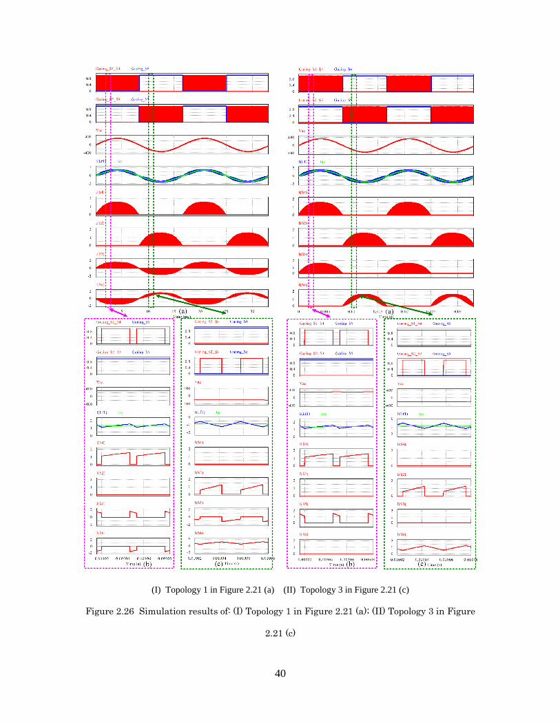
40
(I) Topology 1 in Figure 2.21 (a) (II) Topology 3 in Figure 2.21 (c)
Figure 2.26 Simulation results of: (I) Topology 1 in Figure 2.21 (a); (II) Topology 3 in Figure
2.21 (c)

41
2.4.3 Efficiency calculation and loss analysis
The efficiency calculation and loss analysis are carried out for the proposed
transformerless inverter topology 1 in Figure 2.21 (a). All the power devices in
the inverter are 650V SiC MOSFET with the part umber SCT2120AFC [129].
The inverter is running at 30 kHz switching frequency, the input dc voltage is
380V, the ac output voltage is 240 V, and the nominal output power is 250W.
The losses in the inverter can be divided into the power devices loss (conduction
loss, switching loss), and output inductor loss (winding loss and magnetic core
loss).
The voltage drop of MOSFETs can be simplified as a channel resistor, the
voltage drop of device body diodes can be simplified as a voltage source series
with a channel resistor, which are shown in (2.1) and (2.2) respectively.
ds dsv i R (2.1)
ak f akv V i R (2.2)
Assuming the output current is in-phase with the duty cycle, which refers
to pure active generation condition, the output current can be expressed as:
( ) sin( )mi t I t (2.3)
For the inverter topology 1 in Figure 2.21 (a), all the high frequency
MOSFETs (S1 and S4) power devices work in the positive half of the line cycle.
For the positive half cycle, the duty cycle of S1, S4 can be expressed as(2.4); the
duty cycle of the S5 can be expressed as(2.5).

42
1 4
sin( )S Sd M t (2.4)
5
1- sin( )Sd M t (2.5)
So the conduction loss of S1 or S4 is:
1 4 1 4
2
_ / 0
1 2( ) ( ) ( )
2 3Conduction S S ds S S m ds
MP i t v t d d t I R (2.6)
The channel of the S5 and the body diode of the S6 work in the positive half
of the line cycle. They share the same duty cycle, so the conduction loss on the
channel resistor of S5 and the body diode of S6 is:
5 5
2
_ 0
1 1 2( ) ( ) ( ) ( )
2 4 3Conduction S ds S m ds
MP i t v t d d t I R (2.7)
6 5_ _ 0
2
m m
1( ) ( ) ( )
2
1 1 2I ( ) I ( )
4 4 3
Conduction S Diode ak S
f ak
P i t v t d d t
M MV R
(2.8)
Power losses of the S2, S3 in the negative half cycle are as same the switch
S1 and S4 due to the symmetric operation modes. So, the conduction loss of the
S2 or S3 can be expressed as:
2 3 1 4
2
_ / _ /
2
3Conduction S S Conduction S S m ds
MP P I R (2.9)
The current in the channel of S6 is continuous for the negative half cycle, so
the channel conduction loss can be expressed as:
6
2 2
_
2
2 1 2(
3 4 3
1
4
Conduction S m ds m ds
m ds
M MP I R I R
I R
(2.10)
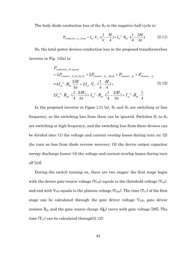
43
The body diode conduction loss of the S5 in the negative half cycle is:
5
2
_ _ m m
1 1 2I ( ) I ( )
4 4 3 Conduction S Diode f ak
M MP V R (2.11)
So, the total power devices conduction loss in the proposed transformerless
inverter in Fig. 12(a) is:
1 2 3 4 5 5 6
_ Pr
_ / / / _ _ _ _
2
2 2 2
4 2
2 1=4 2 ( - )
3 4
1 2 1 2 12 ( - ) ( )
4 3 4 3 4
conduction oposed
Conduct S S S S Conduct S Diode Conduct S Conduct S
m ds m f
m ak m ds m ds
P
P P P P
M MI R I V
M MI R I R I R
(2.12)
In the proposed inverter in Figure 2.21 (a), S5 and S6 are switching at line
frequency, so the switching loss from them can be ignored. Switches S1 to S4
are switching at high frequency, and the switching loss from these devices can
be divided into: (1) the voltage and current overlap losses during turn on; (2)
the turn on loss from diode reverse recovery; (3) the device output capacitor
energy discharge losses; (4) the voltage and current overlap losses during turn
off [43].
During the switch turning on, there are two stages: the first stage begin
with the device gate-source voltage (VGS) equals to the threshold voltage (Vth),
and end with VGS equals to the plateau voltage (Vpla). The time (Tr1) of the first
stage can be calculated through the gate driver voltage VDD, gate driver
resistor Rg, and the gate source charge (Qg) curve with gate voltage [80]. The
time (Tr1) can be calculated through(2.13):
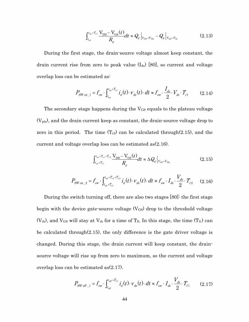
44
1 DD GSV V ( )on r
GS Pla GS thon
t T
g V V g V Vtg
tdt Q Q
R (2.13)
During the first stage, the drain-source voltage almost keep constant, the
drain current rise from zero to peak value (Ids) [80], so current and voltage
overlap loss can be estimated as:
1
_1 1( ) ( )
2
on r
on
t Tds
SW on sw d ds sw ds rt
IP f i t v t dt f V T (2.14)
The secondary stage happens during the VGS equals to the plateau voltage
(Vpla), and the drain current keep as constant, the drain-source voltage drop to
zero in this period. The time (Tr2) can be calculated through(2.15), and the
current and voltage overlap loss can be estimated as(2.16).
1 2
1
DD GSV V ( )on r r
GS Plaon r
t T T
g V Vt Tg
tdt Q
R (2.15)
1 2
1_ 2 2
( ) ( )2
on r r
on r
t T Tds
SW on sw d ds sw ds rt T
VP f i t v t dt f I T (2.16)
During the switch turning off, there are also two stages [80]: the first stage
begin with the device gate-source voltage (VGS) drop to the threshold voltage
(Vth), and VGS will stay at Vth for a time of Tfl. In this stage, the time (Tf1) can
be calculated through(2.15), the only difference is the gate driver voltage is
changed. During this stage, the drain current will keep constant, the drain-
source voltage will rise up from zero to maximum, so the current and voltage
overlap loss can be estimated as(2.17).
1
_1 1( ) ( )
2
off f
off
t Tds
SW off sw d ds sw ds ft
VP f i t v t dt f I T (2.17)

45
The secondary stage happens during the device gate-source voltage (VGS)
drops from the plateau voltage (Vpla) to the threshold voltage (Vth). The time
(Tf2) be calculated through (2.15) with related turn off gate driver voltage.
During this stage, the drain-source voltage will keep constant, the drain
current will drop from maximum to zero, so the current and voltage overlap
loss can be estimated as(2.18).
1 2
1_ 2 2
( ) ( )2
off f f
off f
t T Tds
SW off sw d ds sw ds ft T
IP f i t v t dt f V T (2.18)
During the switch turning on, there is a diode reverse recovery [80], which
will result the loss of:
rr sw dc rrP f V Q (2.19)
Besides, the device output capacitor energy will be discharged in the device
during the device turning on [80], and this output capacitor energy discharge
losses can be calculated as:
Coss sw CossP f E (2.20)
So the total switching loss can be expressed as:
_ 1 2 1 2( )
2ds
SW Loss sw ds r r f f
sw dc rr sw Coss
IP f V T T T T
f V Q f E
(2.21)
The conduction loss in the inductor can be divided in to the line frequency
current conduction loss which is related to the dc resistance RL_DC, and the
switching frequency current ripple conduction loss which is related to the
switching frequency ac resistance RL_AC. The total conduction losses are:
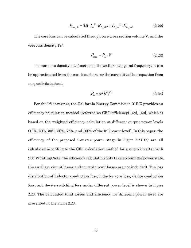
46
2 2
_ _ _ _0.5con L m L DC f ac L ACP I R I R (2.22)
The core loss can be calculated through core cross section volume V, and the
core loss density PL:
core LP P V (2.23)
The core loss density is a function of the ac flux swing and frequency. It can
be approximated from the core loss charts or the curve fitted loss equation from
magnetic datasheet.
b c
LP a B f (2.24)
For the PV inverters, the California Energy Commission (CEC) provides an
efficiency calculation method (referred as CEC efficiency) [48], [49], which is
based on the weighted efficiency calculation at different output power levels
(10%, 20%, 30%, 50%, 75%, and 100% of the full power level). In this paper, the
efficiency of the proposed inverter power stage in Figure 2.23 (a) are all
calculated according to the CEC calculation method for a micro-inverter with
250-W rating(Note: the efficiency calculation only take account the power state,
the auxiliary circuit losses and control circuit losses are not included). The loss
distribution of inductor conduction loss, inductor core loss, device conduction
loss, and device switching loss under different power level is shown in Figure
2.23. The calculated total losses and efficiency for different power level are
presented in the Figure 2.23.
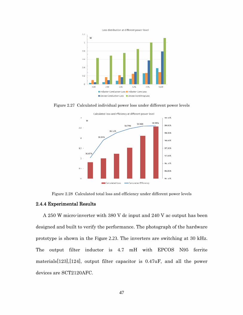
47
Figure 2.27 Calculated individual power loss under different power levels
Figure 2.28 Calculated total loss and efficiency under different power levels
2.4.4 Experimental Results
A 250 W micro-inverter with 380 V dc input and 240 V ac output has been
designed and built to verify the performance. The photograph of the hardware
prototype is shown in the Figure 2.23. The inverters are switching at 30 kHz.
The output filter inductor is 4.7 mH with EPCOS N95 ferrite
materials[123],[124], output filter capacitor is 0.47uF, and all the power
devices are SCT2120AFC.
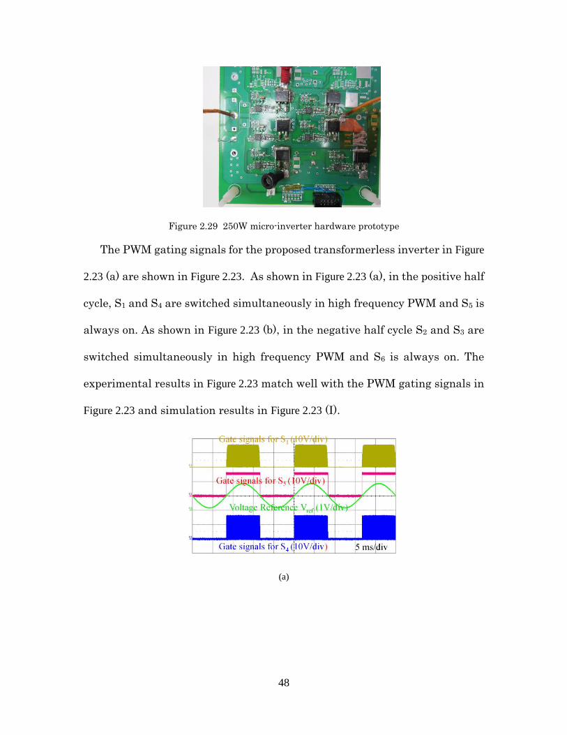
48
Figure 2.29 250W micro-inverter hardware prototype
The PWM gating signals for the proposed transformerless inverter in Figure
2.23 (a) are shown in Figure 2.23. As shown in Figure 2.23 (a), in the positive half
cycle, S1 and S4 are switched simultaneously in high frequency PWM and S5 is
always on. As shown in Figure 2.23 (b), in the negative half cycle S2 and S3 are
switched simultaneously in high frequency PWM and S6 is always on. The
experimental results in Figure 2.23 match well with the PWM gating signals in
Figure 2.23 and simulation results in Figure 2.23 (I).
(a)
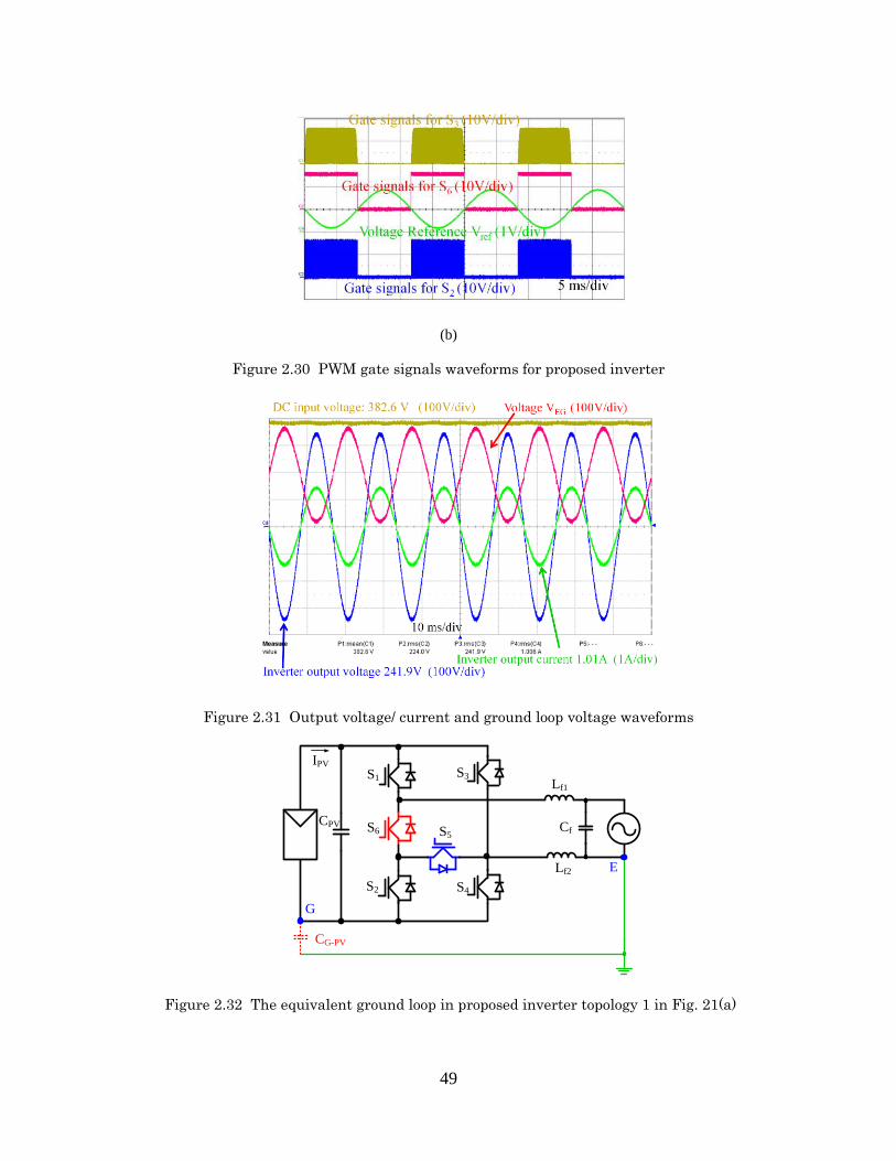
49
(b)
Figure 2.30 PWM gate signals waveforms for proposed inverter
Figure 2.31 Output voltage/ current and ground loop voltage waveforms
IPV
S1
S2 S4
S3
CPV Cf
Lf1
Lf2
S6 S5
E
CG-PV
G
Figure 2.32 The equivalent ground loop in proposed inverter topology 1 in Fig. 21(a)
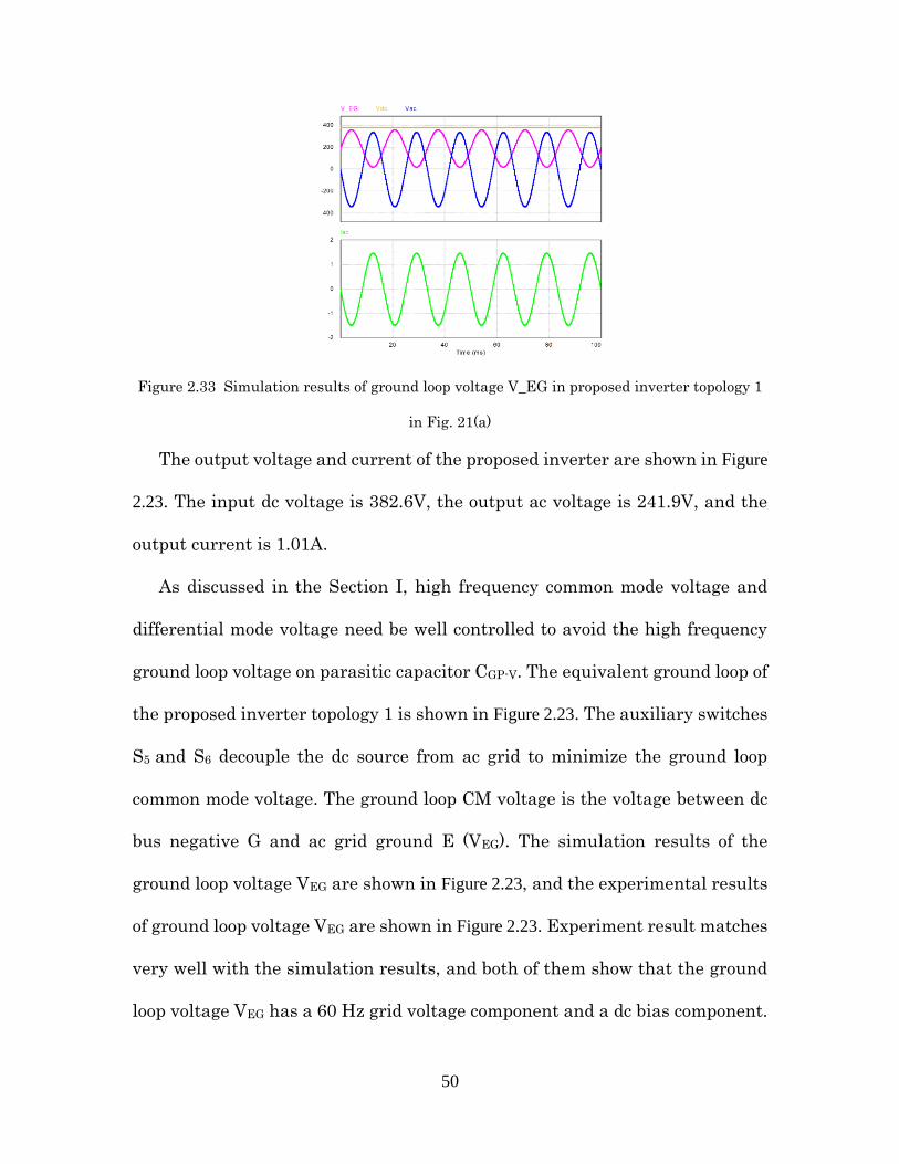
50
Figure 2.33 Simulation results of ground loop voltage V_EG in proposed inverter topology 1
in Fig. 21(a)
The output voltage and current of the proposed inverter are shown in Figure
2.23. The input dc voltage is 382.6V, the output ac voltage is 241.9V, and the
output current is 1.01A.
As discussed in the Section I, high frequency common mode voltage and
differential mode voltage need be well controlled to avoid the high frequency
ground loop voltage on parasitic capacitor CGP-V. The equivalent ground loop of
the proposed inverter topology 1 is shown in Figure 2.23. The auxiliary switches
S5 and S6 decouple the dc source from ac grid to minimize the ground loop
common mode voltage. The ground loop CM voltage is the voltage between dc
bus negative G and ac grid ground E (VEG). The simulation results of the
ground loop voltage VEG are shown in Figure 2.23, and the experimental results
of ground loop voltage VEG are shown in Figure 2.23. Experiment result matches
very well with the simulation results, and both of them show that the ground
loop voltage VEG has a 60 Hz grid voltage component and a dc bias component.
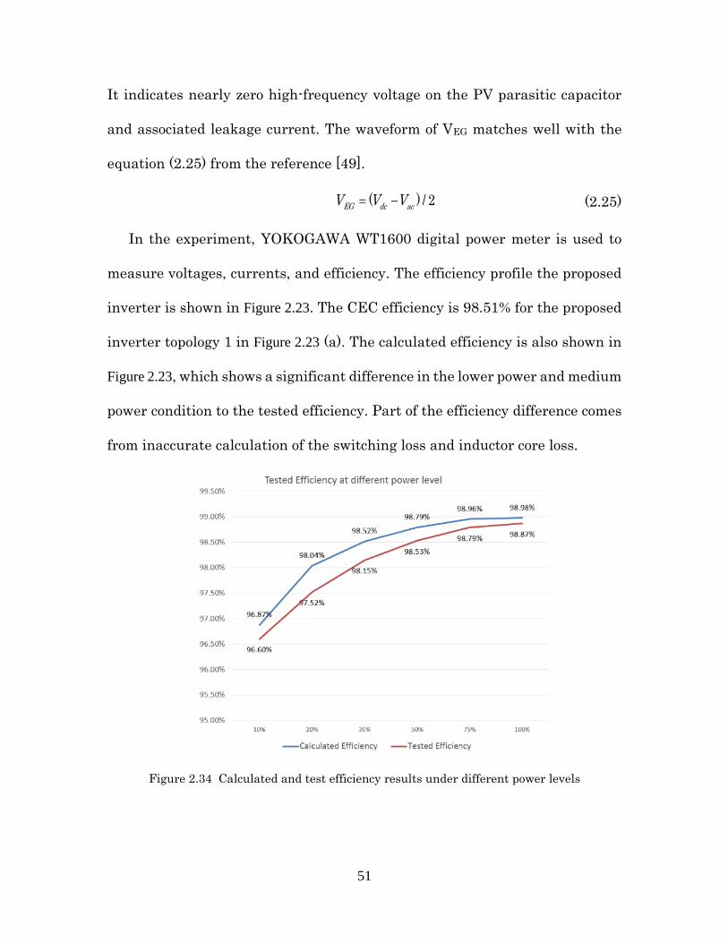
51
It indicates nearly zero high-frequency voltage on the PV parasitic capacitor
and associated leakage current. The waveform of VEG matches well with the
equation (2.25) from the reference [49].
( ) / 2EG dc acV V V (2.25)
In the experiment, YOKOGAWA WT1600 digital power meter is used to
measure voltages, currents, and efficiency. The efficiency profile the proposed
inverter is shown in Figure 2.23. The CEC efficiency is 98.51% for the proposed
inverter topology 1 in Figure 2.23 (a). The calculated efficiency is also shown in
Figure 2.23, which shows a significant difference in the lower power and medium
power condition to the tested efficiency. Part of the efficiency difference comes
from inaccurate calculation of the switching loss and inductor core loss.
Figure 2.34 Calculated and test efficiency results under different power levels
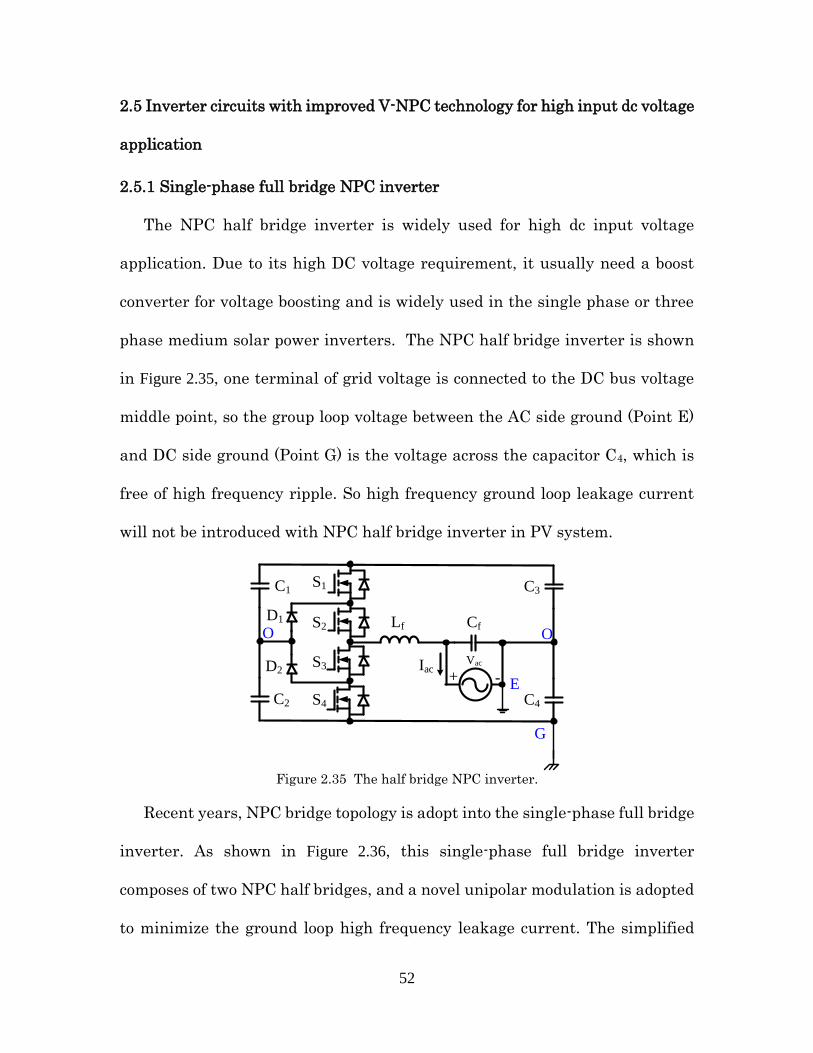
52
2.5 Inverter circuits with improved V-NPC technology for high input dc voltage
application
2.5.1 Single-phase full bridge NPC inverter
The NPC half bridge inverter is widely used for high dc input voltage
application. Due to its high DC voltage requirement, it usually need a boost
converter for voltage boosting and is widely used in the single phase or three
phase medium solar power inverters. The NPC half bridge inverter is shown
in Figure 2.35, one terminal of grid voltage is connected to the DC bus voltage
middle point, so the group loop voltage between the AC side ground (Point E)
and DC side ground (Point G) is the voltage across the capacitor C4, which is
free of high frequency ripple. So high frequency ground loop leakage current
will not be introduced with NPC half bridge inverter in PV system.
S1
S2
S3
S4
C1
Cf
IacVac+
- E
D1
D2
Lf
C2
C3
C4
O O
G
Figure 2.35 The half bridge NPC inverter.
Recent years, NPC bridge topology is adopt into the single-phase full bridge
inverter. As shown in Figure 2.36, this single-phase full bridge inverter
composes of two NPC half bridges, and a novel unipolar modulation is adopted
to minimize the ground loop high frequency leakage current. The simplified
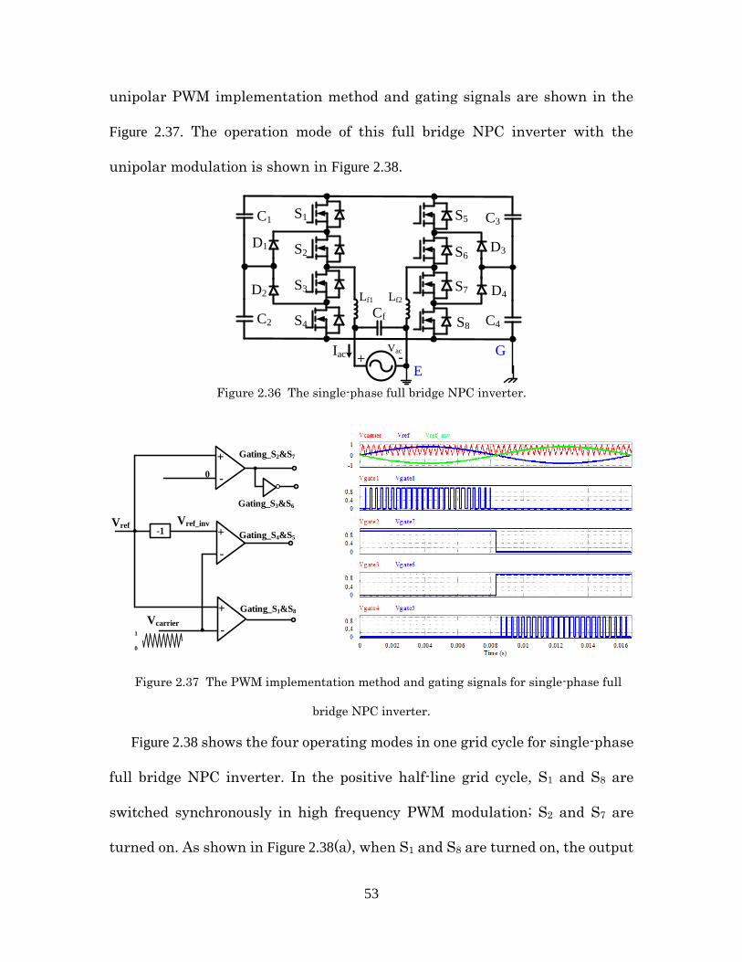
53
unipolar PWM implementation method and gating signals are shown in the
Figure 2.37. The operation mode of this full bridge NPC inverter with the
unipolar modulation is shown in Figure 2.38.
E
S1
S2
S3
S4
S5
S6
S7
S8
Cf
IacVac+
-G
C1
C2
C3
C4
D1
D2
D3
D4Lf1 Lf2
Figure 2.36 The single-phase full bridge NPC inverter.
0
+
-
+
-Vcarrier
Vref-1
+
-
Gating_S1&S8
Gating_S2&S7
Gating_S4&S5
Vref_inv
1
0
Gating_S3&S6
Figure 2.37 The PWM implementation method and gating signals for single-phase full
bridge NPC inverter.
Figure 2.38 shows the four operating modes in one grid cycle for single-phase
full bridge NPC inverter. In the positive half-line grid cycle, S1 and S8 are
switched synchronously in high frequency PWM modulation; S2 and S7 are
turned on. As shown in Figure 2.38(a), when S1 and S8 are turned on, the output
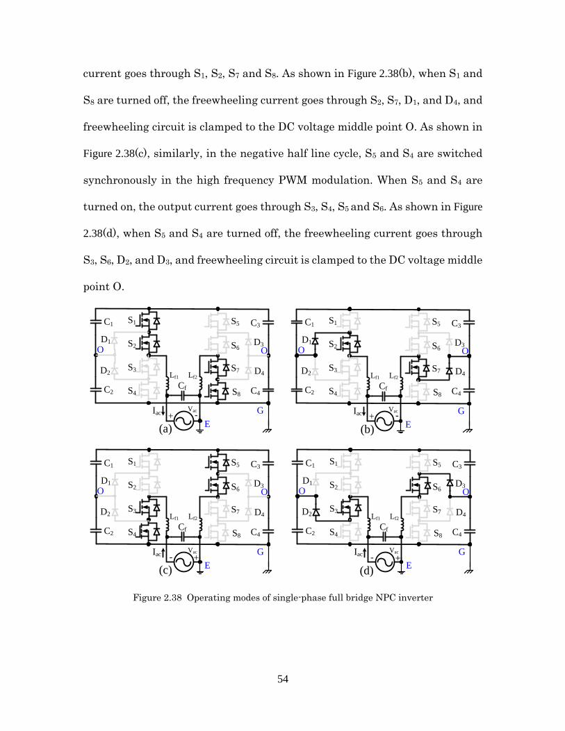
54
current goes through S1, S2, S7 and S8. As shown in Figure 2.38(b), when S1 and
S8 are turned off, the freewheeling current goes through S2, S7, D1, and D4, and
freewheeling circuit is clamped to the DC voltage middle point O. As shown in
Figure 2.38(c), similarly, in the negative half line cycle, S5 and S4 are switched
synchronously in the high frequency PWM modulation. When S5 and S4 are
turned on, the output current goes through S3, S4, S5 and S6. As shown in Figure
2.38(d), when S5 and S4 are turned off, the freewheeling current goes through
S3, S6, D2, and D3, and freewheeling circuit is clamped to the DC voltage middle
point O.
E
S1
S2
S3
S4
S5
S6
S7
S8
Cf
IacVac+
-G
C1
C2
C3
C4
D1
D2
D3
D4Lf1 Lf2
O O
E
S1
S2
S3
S4
S5
S6
S7
S8
Cf
IacVac+
-G
C1
C2
C3
C4
D1
D2
D3
D4Lf1 Lf2
O O
E
S1
S2
S3
S4
S5
S6
S7
S8
Cf
IacVac+
-G
C1
C2
C3
C4
D1
D2
D3
D4Lf1 Lf2
O O
E
S1
S2
S3
S4
S5
S6
S7
S8
Cf
IacVac+
-G
C1
C2
C3
C4
D1
D2
D3
D4Lf1 Lf2
O O
(a) (b)
(c) (d)
Figure 2.38 Operating modes of single-phase full bridge NPC inverter
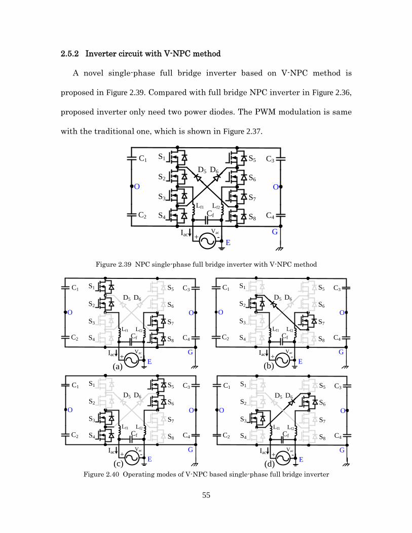
55
2.5.2 Inverter circuit with V-NPC method
A novel single-phase full bridge inverter based on V-NPC method is
proposed in Figure 2.39. Compared with full bridge NPC inverter in Figure 2.36,
proposed inverter only need two power diodes. The PWM modulation is same
with the traditional one, which is shown in Figure 2.37.
S1
S2
S3
S4
S5
S6
S7
S8Cf
IacVac+
-G
E
C1
C2
C3
C4
D5 D6
Lf1 Lf2
O O
Figure 2.39 NPC single-phase full bridge inverter with V-NPC method
S1
S2
S3
S4
S5
S6
S7
S8Cf
IacVac+
-G
E
C1
C2
C3
C4
D5 D6
Lf1 Lf2
O O
S1
S2
S3
S4
S5
S6
S7
S8Cf
IacVac+
-G
E
C1
C2
C3
C4
D5 D6
Lf1 Lf2
O O
S1
S2
S3
S4
S5
S6
S7
S8Cf
IacVac+
-G
E
C1
C2
C3
C4
D5 D6
Lf1 Lf2
O O
S1
S2
S3
S4
S5
S6
S7
S8Cf
IacVac+
-G
E
C1
C2
C3
C4
D5 D6
Lf1 Lf2
O O
(a) (b)
(c) (d) Figure 2.40 Operating modes of V-NPC based single-phase full bridge inverter

56
The operating model of this V-NPC technology based single-phase full
bridge inverter is shown in Figure 2.40. As shown in Figure 2.40(a), when S1 and
S8 are turned on, the output current goes through S1, S2, S7 and S8. As shown
in Figure 2.40(b), when S1 and S8 are turned off, the freewheeling current goes
through D5. As shown in Figure 2.40(c), similarly, When S5 and S4 are turned
on, the output current goes through S3, S4, S5 and S6. As shown in Figure 2.40(d),
when S5 and S4 are turned off, the freewheeling current goes through D6.
2.5.3 A family of inverter circuits with improved V-NPC method
Compared with the traditional full bridge NPC inverter, the proposed V-
NPC based inverter topology only has two power diode, which means lower
conduction loss, higher efficiency, and smaller package. But power circuit will
not be clamped to a fixed power level during current freewheeling. In
theoretically, if the power devices, gating voltages and gating speed are totally
same and the power loop are perfect symmetrical, the power loop of proposed
inverter during freewheeling will be clamped to the half of dc bus voltage. In
practical, these condition cannot be guaranteed. In order to clamp the proposed
inverter to a fixed power level during freewheeling, addition four clamping
diodes (can be other clamping circuit) are added in to the proposed inverter,
which is shown in Figure 2.41(a). these four clamping diode are just for power
level clamping, should has no power consuming, and the package can be
negligible compared with the power diode D5 and D6. Another three inverter
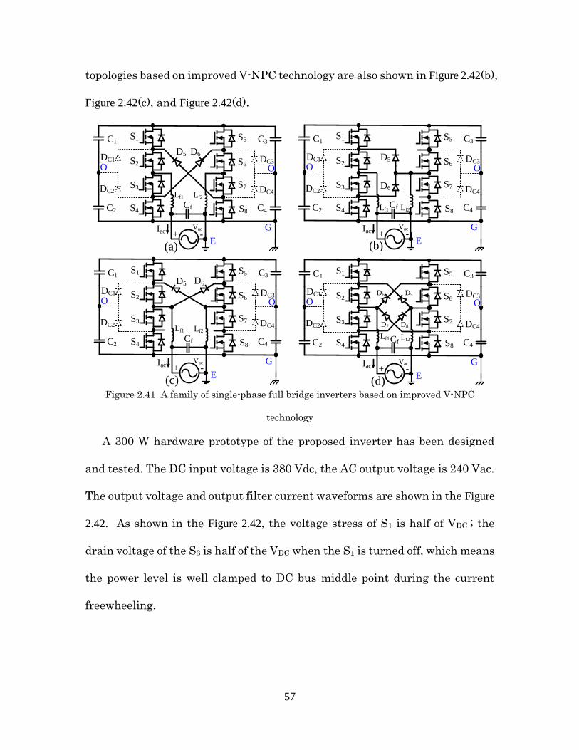
57
topologies based on improved V-NPC technology are also shown in Figure 2.42(b),
Figure 2.42(c), and Figure 2.42(d).
S1
S2
S3
S4Cf
IacVac+
-E
G
C1
C2
C3
C4
Lf1 Lf2
S5
S6
S7
S8
D5 D6
DC1
DC2
DC3O O
DC4
S1
S2
S3
S4Cf
IacVac+
-E
G
C1
C2
C3
C4Lf1 Lf2
S5
S6
S7
S8
D5
D6
DC1
DC2
DC3O O
DC4
S1
S2
S3
S4Cf
IacVac+
-E
G
C1
C2
C3
C4
Lf1 Lf2
S5
S6
S7
S8
DC1
DC2
DC3O O
DC4D7
D5D6
D8
S1
S2
S3
S4Cf
IacVac+
-E
G
C1
C2
C3
C4
Lf1 Lf2
S5
S6
S7
S8
D5 D6DC1
DC2
DC3O O
DC4
(a) (b)
(c) (d) Figure 2.41 A family of single-phase full bridge inverters based on improved V-NPC
technology
A 300 W hardware prototype of the proposed inverter has been designed
and tested. The DC input voltage is 380 Vdc, the AC output voltage is 240 Vac.
The output voltage and output filter current waveforms are shown in the Figure
2.42. As shown in the Figure 2.42, the voltage stress of S1 is half of VDC ; the
drain voltage of the S3 is half of the VDC when the S1 is turned off, which means
the power level is well clamped to DC bus middle point during the current
freewheeling.
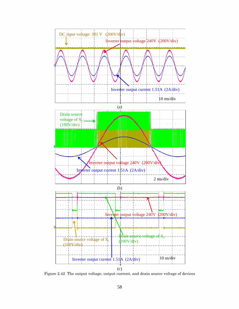
58
Inverter output voltage 240V (200V/div)
Inverter output current 1.51A (2A/div)
DC input voltage: 381 V (200V/div)
10 ms/div
(a)
Inverter output voltage 240V (200V/div)
Inverter output current 1.51A (2A/div)
2 ms/div
Drain source
voltage of S3
(100V/div)
(b)
Drain source voltage of S1
(100V/div)
Drain source voltage of S3
(100V/div)
Inverter output current 1.51A (2A/div)
Inverter output voltage 240V (200V/div)
10 us/div
(c)
Figure 2.42 The output voltage, output current, and drain source voltage of devices
59
2.6 Summary
Compared with the traditional inverter with transformers, the
transformerless inverter topology can achieves higher efficiency, smaller
volume, and lower cost. For the high power and high input voltage application,
the NPC topology is widely used. For the lower power and low input voltage
single-phase transformerless inverter, there are a lot new inverter topologies
for better performance than traditional H-bridge inverter.
With the overview of the state-of-the-art transfomerless inverter, a new
inverter technology is summarized in this dissertation, which is the
improvement of the traditional NPC technology and called V-NPC technology.
Based on this new technology, a family of high-efficiency single phase
transformerless inverters are present in this dissertation. The PWM method
and working principle are described, the circuit efficiency is also analyzed and
tested with hardware prototype, which demonstrate the 98.96% peak efficiency
at full load condition of 250W.
For the high dc input single phase transformerless inverter, the V-NPC
technology can be further improved. With the improved V-NPC technology, a
family single-phase inverters are proposed, experimental results also
demonstrate the validity, and this can be interest topic for future work.
60
Chapter 3 MOSFET based Transformerless Inverter Circuit with
High Magnetic Utilization
3.1 Introduction
In recent years, single-phase transformerless PV inverter products are
becoming more and more popular. For efficiency consideration and standards
compliance, a variety of inverter topologies have been adopted [32]-[61].For the
lower power level transformerless inverters, most of the innovative topologies
use super junction metal oxide semiconductor field effect transistor (MOSFET)
to boost efficiency [48]-[61].
The complimentary phase-leg with CoolMOS is shown Figure 3.1 (a). The
super-junction metal oxide semiconductor field effect transistor’s (SJ-MOSFET
or CoolMOS) voltage drop is resistive and is preferred for maintaining high
efficiency under light-load conditions and also for fast switching speed.
However, high-voltage CoolMOS suffers from slow reverse recovery of its
snappy body diode, which not only produces high dv/dt, di/dt, and high power
loss, but also creates phase-leg shoot through risk [84]-[89]. Therefore, high-
voltage MOSFETs based phase-leg with top and bottom complimentary devices
is not suitable for hard switching applications.
High efficiency power converters can be achieved by using CoolMOS and
Silicon Schottky Carbide (SiC) diode. Typical examples are boost converters
and buck converters (as shown in Figure 3.1(b)); in which, the snappy body diode
will not conduct current under unidirectional current flowing. The reverse
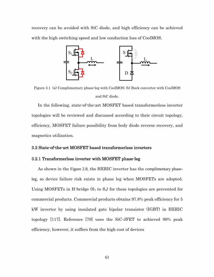
61
recovery can be avoided with SiC diode, and high efficiency can be achieved
with the high switching speed and low conduction loss of CoolMOS.
L
S1
S2
D
S
L
Figure 3.1 (a) Complimentary phase-leg with CoolMOS; (b) Buck converter with CoolMOS
and SiC diode.
In the following, state-of-the-art MOSFET based transformerless inverter
topologies will be reviewed and discussed according to their circuit topology,
efficiency, MOSFET failure possibility from body diode reverse recovery, and
magnetics utilization.
3.2 State-of-the-art MOSFET based transformerless inverters
3.2.1 Transformerless inverter with MOSFET phase-leg
As shown in the Figure 2.8, the HERIC inverter has the complimentary phase-
leg, so device failure risk exists in phase leg when MOSFETs are adopted.
Using MOSFETs in H-bridge (S1 to S4) for these topologies are prevented for
commercial products. Commercial products obtains 97.8% peak efficiency for 5
kW inverter by using insulated gate bipolar transistor (IGBT) in HERIC
topology [117]. Reference [79] uses the SiC-JFET to achieved 99% peak
efficiency, however, it suffers from the high cost of devices

62
As shown in Figure 2.8. H5 topology of SMA [59], which only needs 3
MOSFETs and 2 IGBTs, decouples the PV panel from grid with two middle
IGBTs during the current freewheeling period. The MOSFET failure risk from
body diode reverse recovery can be eliminated by splitting MOSFET phase leg
with two IGBTs. However, the conduction loss will be a little higher than
HERIC topology due to 3 devices are in the conduction loop and fixed voltage
drop of IGBTs.
As shown in Figure 2.8, H6 topology will still have complimentary phase-leg, so
device failure risk exists in phase leg when MOSFETs are adopted. Besides,
the symmetrical H6 topology in Figure 2.8 and hybrid phase-leg inverter
topology in Figure 2.8 both have the complimentary phase-leg, so the high voltage
MOSFETs are not suggested for these inverters.
As shown in Figure 3.2, the two stage topology with pseudo DC link, which
can achieve high efficiency by adopting MOSFET in the first stage, operates S5
and S6 in high frequency and S1 to S4 in lower frequency. With proper operation
of S5 and S6, system switching loss could be optimized. This method is adopted
in the commercial product and obtains 98% peak efficiency and 97.5% CEC
efficiency [40]. The drawbacks of this topology are still too many switches and
high conduction loss (4 devices in conduction loop). The low frequency devices
S1 to S4 also have diode reverse recovery risk during the current zero-crossing,
and MOSFETs is not suggestion for S1 to S4.
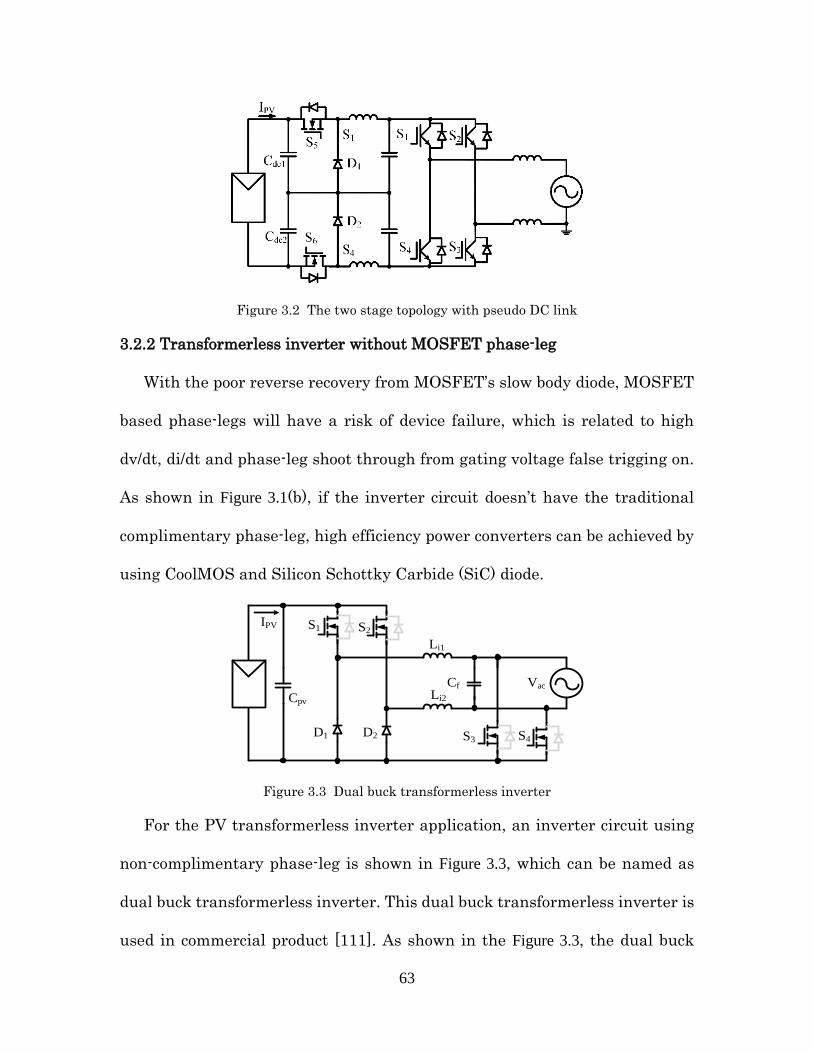
63
Figure 3.2 The two stage topology with pseudo DC link
3.2.2 Transformerless inverter without MOSFET phase-leg
With the poor reverse recovery from MOSFET’s slow body diode, MOSFET
based phase-legs will have a risk of device failure, which is related to high
dv/dt, di/dt and phase-leg shoot through from gating voltage false trigging on.
As shown in Figure 3.1(b), if the inverter circuit doesn’t have the traditional
complimentary phase-leg, high efficiency power converters can be achieved by
using CoolMOS and Silicon Schottky Carbide (SiC) diode.
IPV
Cpv
D1
S2
D2
S1
Li1
S4
Vac
Li2
Cf
S3
Figure 3.3 Dual buck transformerless inverter
For the PV transformerless inverter application, an inverter circuit using
non-complimentary phase-leg is shown in Figure 3.3, which can be named as
dual buck transformerless inverter. This dual buck transformerless inverter is
used in commercial product [111]. As shown in the Figure 3.3, the dual buck

64
inverter needs four CoolMOS and two Schottky diodes, and the CoolMOS phase
leg is split into two independent buck converters by two filter inductors (S1 and
S3 are split with Li1; S2 and S4 are split with Li2), so the body diode of CoolMOS
will not conduct, and the reverse recovery issues can be avoided. In addition,
this inverter can use unipolar modulation to achieve low common mode
voltage. With CoolMOS / SiC-diode and unipolar modulation, the inverter can
get 99% over a wide load range [41]. The major drawbacks of this inverter are
(1) an additional large-size inductor, which has 50% the utilization because
each inductor only conducts either positive or negative line cycle, and (2) it is
not possible to realize reactive power generation because it only allows
unidirectional power flow from dc to ac.
The bidirectional dual buck inverter [56], which is patented by Xantrex
Technology Inc, provides another way for high reliability and high efficiency
MOSFET inverter design. As shown in Figure 3.4, the dual buck inverter uses
four output filter inductors to split the MOSFET phase legs. The snappy body
diode of MOSFET will not conduct current under unidirectional current
flowing. The reverse recovery can be avoided with SiC diode, and high
efficiency can be achieved with the high switching speed and low conduction
loss of CoolMOS. But this inverter needs to use bipolar modulation to minimize
the common mode voltage for a transformerless inverter application [56], [66],
[ 67]. Thus this inverter pays for its high reliability with lower efficiency and
50% magnetic utilization.
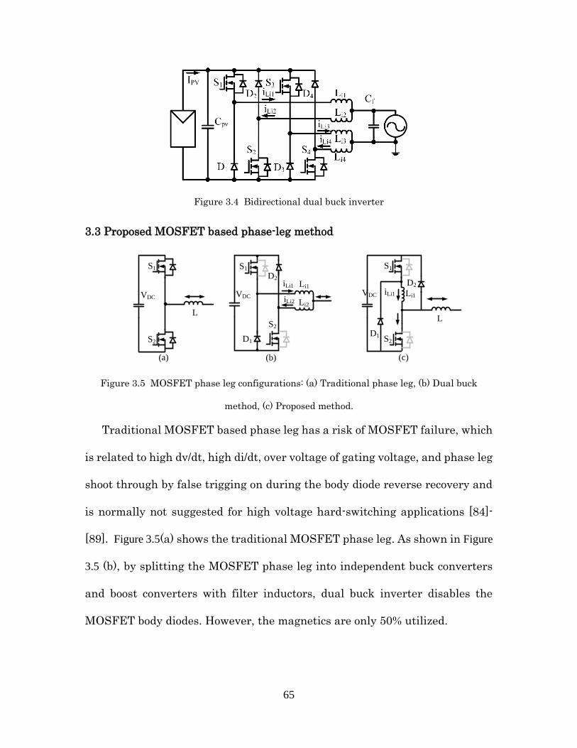
65
Figure 3.4 Bidirectional dual buck inverter
3.3 Proposed MOSFET based phase-leg method
S1
S2
VDC
L
(a)
Li1
Li2
S1
D1
S2
D2iLi1
iLi2VDC
(b)
S1
S2
VDC Li1iLi1
L
D1
D2
(c)
Figure 3.5 MOSFET phase leg configurations: (a) Traditional phase leg, (b) Dual buck
method, (c) Proposed method.
Traditional MOSFET based phase leg has a risk of MOSFET failure, which
is related to high dv/dt, high di/dt, over voltage of gating voltage, and phase leg
shoot through by false trigging on during the body diode reverse recovery and
is normally not suggested for high voltage hard-switching applications [84]-
[89]. Figure 3.5(a) shows the traditional MOSFET phase leg. As shown in Figure
3.5 (b), by splitting the MOSFET phase leg into independent buck converters
and boost converters with filter inductors, dual buck inverter disables the
MOSFET body diodes. However, the magnetics are only 50% utilized.

66
Considering the MOSFET body diode reverse recovery risk in Figure 3.5 (a),
and 50% magnetics utilization in Figure 3.5 (b), an improved circuit is proposed
in Figure 3.5 (c). The basic idea of the proposed method is splitting the
traditional MOSFET phase leg with a small phase-leg splitting inductor which
serves two functions: the first function is disabling the MOSFET body diode by
splitting the phase leg into an independent buck converter and boost converter
under normal working conditions, and the second function is protecting
MOSFETs by minimizing the di/dt and dv/dt even when an unexpected
MOSFET body diode reverse recovery happens under abnormal conditions.
The design of this phase-leg splitting inductor will be based on when MOSFET
body diodes have reverse recovery under abnormal conditions, which can be
output current is not well controlled in phase with grid voltage or sudden
disturbance from grid side or dc input side.
In order to verify the proposed MOSFET based phase leg circuit under
MOSFET body diode reverse recovery, two simulations are done in the
SIMetrix by using the PSpice model of IPB60R099C6 [125]. The simulation
adopts the double pulse method for device testing, which is shown in Figure 3.6.
The dc voltage is 380 V, the inductor value is 4.5 mH, and the gating resistor
is 4 Ω. In order to study the di/dt effect on gating voltage, a 5 nH common
source inductance LCSI, which comes from the device lead and the printed
circuit board trace, is introduced in the circuit [84-86]. By turning on the
bottom MOSFET, the inductor current will be charged to about 0.7 A. Then by
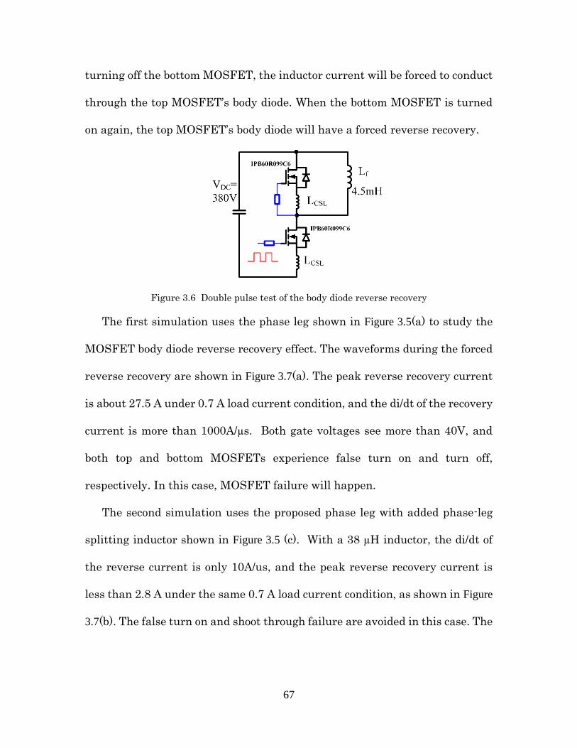
67
turning off the bottom MOSFET, the inductor current will be forced to conduct
through the top MOSFET’s body diode. When the bottom MOSFET is turned
on again, the top MOSFET’s body diode will have a forced reverse recovery.
Figure 3.6 Double pulse test of the body diode reverse recovery
The first simulation uses the phase leg shown in Figure 3.5(a) to study the
MOSFET body diode reverse recovery effect. The waveforms during the forced
reverse recovery are shown in Figure 3.7(a). The peak reverse recovery current
is about 27.5 A under 0.7 A load current condition, and the di/dt of the recovery
current is more than 1000A/µs. Both gate voltages see more than 40V, and
both top and bottom MOSFETs experience false turn on and turn off,
respectively. In this case, MOSFET failure will happen.
The second simulation uses the proposed phase leg with added phase-leg
splitting inductor shown in Figure 3.5 (c). With a 38 µH inductor, the di/dt of
the reverse current is only 10A/us, and the peak reverse recovery current is
less than 2.8 A under the same 0.7 A load current condition, as shown in Figure
3.7(b). The false turn on and shoot through failure are avoided in this case. The
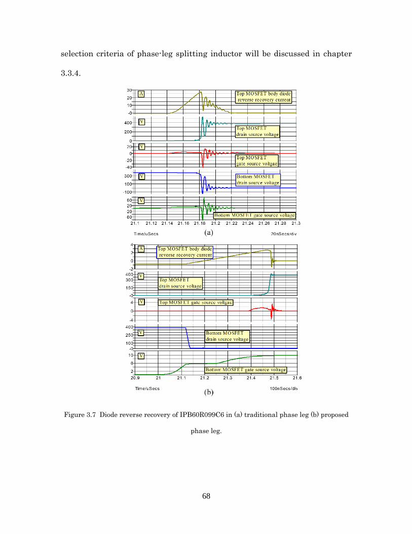
68
selection criteria of phase-leg splitting inductor will be discussed in chapter
3.3.4.
Figure 3.7 Diode reverse recovery of IPB60R099C6 in (a) traditional phase leg (b) proposed
phase leg.
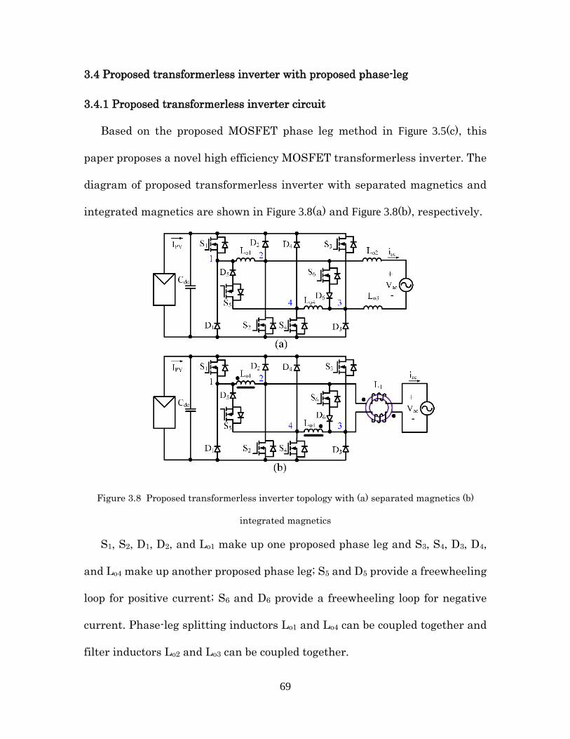
69
3.4 Proposed transformerless inverter with proposed phase-leg
3.4.1 Proposed transformerless inverter circuit
Based on the proposed MOSFET phase leg method in Figure 3.5(c), this
paper proposes a novel high efficiency MOSFET transformerless inverter. The
diagram of proposed transformerless inverter with separated magnetics and
integrated magnetics are shown in Figure 3.8(a) and Figure 3.8(b), respectively.
Figure 3.8 Proposed transformerless inverter topology with (a) separated magnetics (b)
integrated magnetics
S1, S2, D1, D2, and Lo1 make up one proposed phase leg and S3, S4, D3, D4,
and Lo4 make up another proposed phase leg; S5 and D5 provide a freewheeling
loop for positive current; S6 and D6 provide a freewheeling loop for negative
current. Phase-leg splitting inductors Lo1 and Lo4 can be coupled together and
filter inductors Lo2 and Lo3 can be coupled together.

70
The phase-leg splitting inductors Lo1 and Lo4 have 50% utilization, but the
filter inductors Lo2 and Lo3 have full utilization. The phase-leg splitting
inductors Lo1 and Lo4 are only designed for di/dt suppression with a value much
smaller than the filter inductance. In this paper, the total inductance of phase-
leg splitting inductor is 86 µH, and the filter inductors Lo2 and Lo3 are 4.7 mH.
So even though the phase-leg splitting inductors only have 50% utilization, the
overall inductance utilization is over 98%. Compared with inverter topologies
in Figure 3.3 and Figure 3.4, whose magnetics only have 50% utilization, the
proposed inverter almost achieves almost full utilization of magnetics. Thus
the cost and volume of magnetics can almost be reduced by half. In addition,
the proposed inverter still does not need PWM dead-time, only has two devices
in the conduction loss, and has no risk from reverse recovery of MOSFET body
diodes.
3.4.2 PWM method and operating modes
Figure 3.9 shows the PWM implementation circuit scheme for the proposed
transformerless inverter. Figure 3.10 shows the PWM signals in time domain.
In the positive half grid cycle, voltage reference signal Vref is compared with
the carrier signal Vcarrier, and the output signal is used to drive the devices S1
and S4, which are switched simultaneously in high frequency; voltage reference
signal Vref is compared with 0 and outputs a high level signal to turn on S5 in
the entire positive grid cycle, which operates as a polarity selection in grid line
frequency.
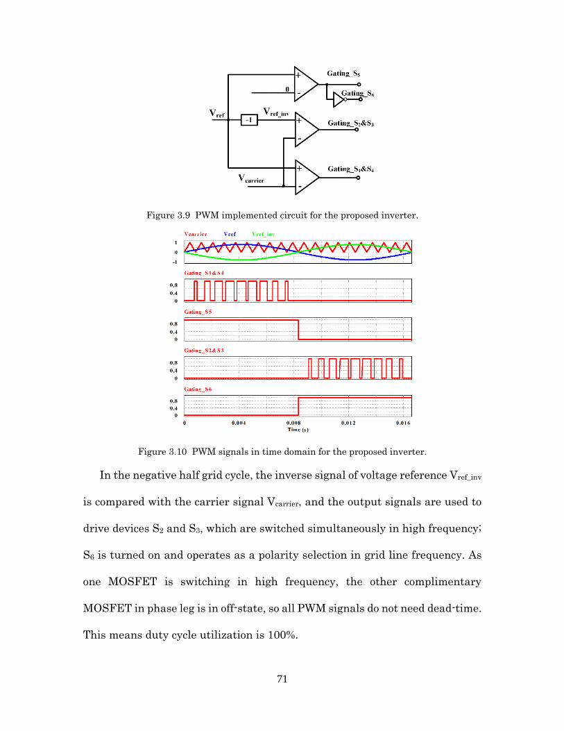
71
Figure 3.9 PWM implemented circuit for the proposed inverter.
Figure 3.10 PWM signals in time domain for the proposed inverter.
In the negative half grid cycle, the inverse signal of voltage reference Vref_inv
is compared with the carrier signal Vcarrier, and the output signals are used to
drive devices S2 and S3, which are switched simultaneously in high frequency;
S6 is turned on and operates as a polarity selection in grid line frequency. As
one MOSFET is switching in high frequency, the other complimentary
MOSFET in phase leg is in off-state, so all PWM signals do not need dead-time.
This means duty cycle utilization is 100%.

72
Figure 3.11 shows the four operating modes in one grid cycle for the proposed
inverter. In the positive half-line grid cycle, S1 and S4 are switched
synchronously in high frequency PWM modulation; S5 is turned on. As shown
in Figure 3.11 (a), when S1 and S4 are turned on, D5 is reverse-biased, the output
current goes through S1 and S4. As shown in Figure 3.11 (b), when S1 and S4 are
turned off, D5 is forward-biased and the freewheeling current goes through S5
and D5. In the positive half line cycle, both filter and phase-leg splitting
inductors conduct current.
Similarly, in the negative half line cycle, S2 and S3 are switched
synchronously in the high frequency PWM modulation; S6 is turned on. As
shown in Figure 3.11 (c), when S2 and S3 are turned on, D6 is reverse-biased, the
output current goes through S2 and S3. As shown in Figure 3.11 (d), when S2 and
S3 are turned off, D6 is forward-biased and the freewheeling current goes
through S6 and D6. In the negative half line cycle, phase-leg splitting inductors
do not need to conduct. Therefore, the phase-leg splitting inductors have 50%
utilization, but filter inductors are fully utilized.
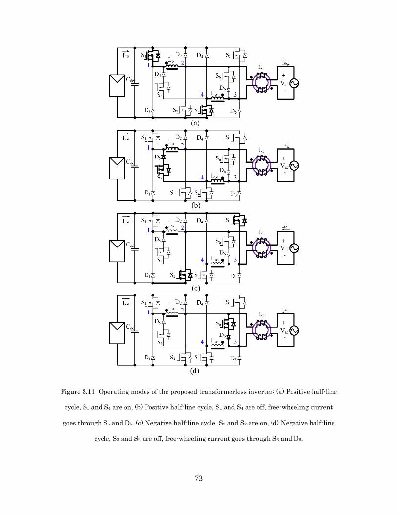
73
Figure 3.11 Operating modes of the proposed transformerless inverter: (a) Positive half-line
cycle, S1 and S4 are on, (b) Positive half-line cycle, S1 and S4 are off, free-wheeling current
goes through S5 and D5, (c) Negative half-line cycle, S3 and S2 are on, (d) Negative half-line
cycle, S3 and S2 are off, free-wheeling current goes through S6 and D6.

74
3.4.3 Ground loop voltage analysis
In the transformerless PV inverter system, there is a parasitic capacitance
exists between the PV array cells and the metal frame [62-74]. The PV array
cells are connected to the dc bus (point G in Figure 3.12); the PV metal frame is
still grounded (point E in Figure 3.12). So this parasitic capacitance, which is
referred as CG-PV in the Figure 3.12, will exist in the ground loop. If the high
frequency common mode voltage (CM) voltage and differential mode (DM)
voltage are not well controlled, there will be a high frequency ground loop
voltage on this parasitic capacitor, and high frequency leakage current will be
generated in turn. This leakage current can cause distortion and harmonic,
high losses, safety issue, fault protection and electron magnetic interference.
The requirements for limiting ground loop leakage current and fault current
can be referred to VDE0126-1-1, and UL 1741[27], [28]. If inverter circuit and
PWM modulation are not well designed, bulk CM filter and DM filter are need
to minimize the ground loop CM voltage. If the ground loop CM voltage is free
of high frequency voltage component, the CM filter and DM filter can be
minimized designed to reduce the size and cost. This Section will analyze the
ground loop voltage of improved inverter under proposed PWM modulation
method. Analysis results will guide the circuit components design for low
ground loop CM voltage.
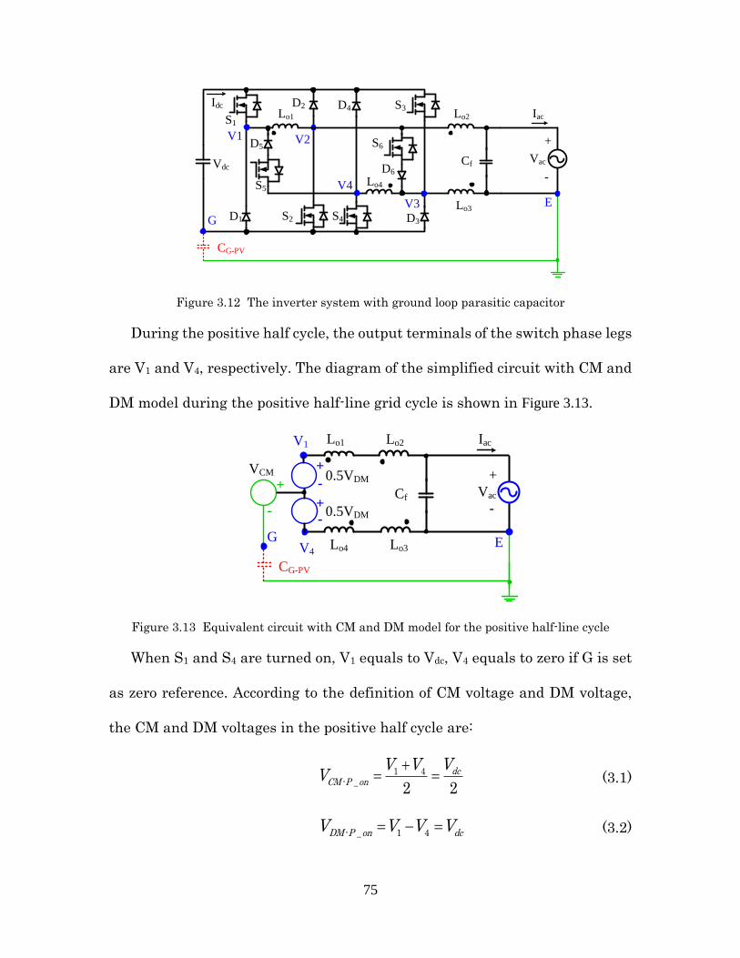
75
Lo1 Iac
Vac
Lo2
Lo3
Lo4
S1
S4
S3
D1
D4
D3S2
D2
S5
S6D5
D6
Idc
Vdc
G
E
+
-
V1 V2
V3
V4
CG-PV
Cf
Figure 3.12 The inverter system with ground loop parasitic capacitor
During the positive half cycle, the output terminals of the switch phase legs
are V1 and V4, respectively. The diagram of the simplified circuit with CM and
DM model during the positive half-line grid cycle is shown in Figure 3.13.
Vac
Lo2
Lo3 E
+
-
V1
Lo4V4
Lo1
CG-PV
G
0.5VDM
0.5VDM
VCM
-+
+
-+
-
Cf
Iac
Figure 3.13 Equivalent circuit with CM and DM model for the positive half-line cycle
When S1 and S4 are turned on, V1 equals to Vdc, V4 equals to zero if G is set
as zero reference. According to the definition of CM voltage and DM voltage,
the CM and DM voltages in the positive half cycle are:
1 4- _
2 2dc
CM P on
VV VV (3.1)
- _ 1 4DM P on dcV V V V (3.2)
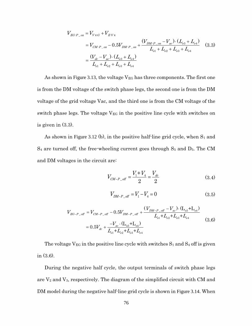
76
- _ 4- - 4
- _ 3 4
- _ - _
1 2 3 4
3 4
1 2 3 4
( ) ( )0.5
( ) ( )
EG P on V G E V
DM P on ac o o
CM P on DM P on
o o o o
dc ac o o
o o o o
V V V
V V L LV V
L L L L
V V L L
L L L L
(3.3)
As shown in Figure 3.13, the voltage VEG has three components. The first one
is from the DM voltage of the switch phase legs, the second one is from the DM
voltage of the grid voltage Vac, and the third one is from the CM voltage of the
switch phase legs. The voltage VEG in the positive line cycle with switches on
is given in (3.3).
As shown in Figure 3.12 (b), in the positive half-line grid cycle, when S1 and
S4 are turned off, the free-wheeling current goes through S5 and D5. The CM
and DM voltages in the circuit are:
1 4
_
+
2 2dc
CM P off
VV VV (3.4)
_ 1 40DM P offV V V (3.5)
_ o3 o4
_ _ _
1 2 3 4
o3 o4
1 2 3 4
( ) (L +L )0.5
+ + +
(L +L )0.5
+ + +
DM P off ac
EG P off CM P off DM P off
o o o o
acdc
o o o o
V VV V V
L L L L
VV
L L L L
(3.6)
The voltage VEG in the positive line cycle with switches S1 and S4 off is given
in (3.6).
During the negative half cycle, the output terminals of switch phase legs
are V2 and V3, respectively. The diagram of the simplified circuit with CM and
DM model during the negative half-line grid cycle is shown in Figure 3.14. When
77
S2 and S3 are turned on, V3 equals to Vdc, V2 equals to zero if G is set as zero
reference.
When the S2 and S3 are turned on, the CM and DM voltage are:
3 2
_
+
2 2dc
CM N on
V V VV (3.7)
_ 3 2DM N on dcV V V V (3.8)
- _ 3- - 3
- _ 3
- _ - _
2 3
3
2 3
( )0.5
( )
EG N on V G E V
DM N on ac o
CM N on DM N on
o o
dc ac odc
o o
V V V
V V LV V
L L
V V LV
L L
(3.9)
The voltage VEG in the negative line cycle with switches S2 and S3 on is given
in (3.9):
Vac
Lo2
Lo3
E+
-
V2
V3
CG-PV
G
VCM 0.5VDM
0.5VDM
Cf
+
-+
+
-
-
Iac
Figure 3.14 Equivalent circuit with CM and DM model for the negative half-line cycle
As shown in Figure 3.12 (d), in the negative half-line grid cycle, when S2 and
S3 are turned off, the free-wheeling current goes through S6 and D6. The CM
and DM voltages in the circuit are:
78
3 2
_
+
2 2dc
CM N off
V V VV (3.10)
_ 3 20DM N offV V V (3.11)
The voltage VEG in the negative line cycle with switches S2 and S3 off is
given in (3.12).
_ o3
_ _ _
2 3
o3
2 3
( ) L0.5
+
L0.5
+
DM N off ac
EG N off CM N off DM N off
o o
acdc
o o
V VV V V
L L
VV
L L
(3.12)
In the proposed inverter, if the inductance Lo2 and Lo3 have the same value
and Lo1 and Lo4 have the same value, VEG comes out to be the same in four
different operating modes according to (3.3), (3.6), (3.9), and (3.12), that is:
- _ _ - _ _2
dc acEG P on EG P off EG N on EG N off
V VV V V V (3.13)
If the phase-leg splitting inductors (Lo1 and Lo4) or filter inductors (Lo2 and
Lo3) are not symmetrically designed, the DM and CM voltages will bring high
frequency voltage to VEG. In order to minimize the high frequency leakage
current, Lo2 and Lo3 are designed with one coupled inductor, Lo1 and Lo4 are
designed with another coupled inductor, which allows a better matching
between Lo2 and Lo3 and between Lo1 and Lo4. As a result, the voltage VEG will
be a line frequency sinusoidal voltage with a dc offset, which is shown in (3.13)
. The experimental VEG waveform will be shown in Part VI, which should verify
the validity of the analysis in this section.

79
3.4.4 Component selection and loss analysis
The output filter of this inverter design is based on the maximum ripple
current. As shown in(3.14), the maximum ripple current is usually designed to
be around 10% to 30% of rated current, which is about 1.04 A (1.47 A peak
value) for 240 V output voltage and 250 W rated output power. The ripple
current is a function of dc voltage, ac grid voltage, filter inductor value, and
PWM turn on time, which is presented in (3.15).
-max
(10% ~ 30%)ripple ratedi I (3.14)
( ) ( )
2 dc ac dc dcripple on
filter filter sw
V V V D V Di T
L L f (3.15)
The proposed inverter is designed to work at 30 kHz switching frequency,
and the inverter output filter inductor is designed to have 25% maximum
current ripple, which is 0.37 A. The maximum current ripple happens at duty
cycle equals to 0.5. Through (3.15), the output filter inductance is calculated to
be 4.3 mH.
RM 14 low profile magnetic cores with N95 ferrite material from EPCOS
are selected for the output filter [123]. Proper gap lgap is used to prevent the
maximum flux density Bmax from saturating under the maximum current
condition. The relationship of maximum flux density with turns N, maximum
current Imax, and gap is shown in (3.16). The relationship between inductance
value Lfilter and gap distance is shown in(3.16). Finally, 4.3 mH inductance is
achieved through 91 turns, which can achieve 23% maximum current ripple.
80
mmax
0
I ax
gap
NB
l
u
(3.16)
2 2
0 0
filtergap gape
e i e e
N NL
l ll
u A u A u A
(3.17)
The filter capacitor design is based on the cut-off frequency of the output
filter, which is usually around 10% to 20% of the switching frequency, the
selection of filter capacitor can follow(3.18). The 0.47 µF capacitor is selected
as the output filter capacitor for the 30 kHz switching frequency in proposed
inverter, which achieves 3.4 kHz cut-off frequency with the filter inductor.
1(10% ~ 20%)
2sw
filter filter
fL C
(3.18)
As mentioned in the Chapter 3.3, the design of phase-leg splitting inductor
L01 and L04 should be based on the worst condition. The worst condition is when
the top MOSFET S1 and bottom MOSFET S2 have a hard commutation through
L01.
The design criterion of phase-leg splitting inductor is mainly to set the limit
of the di/dt for the MOSFET body diode reverse recovery current under
abnormal conditions to avoid false turn on and partial shoot through. For the
selected MOSFET IPB60R099C6 [125], as shown in Figure 3.7 (b), the gate
plateau voltage is around 5.4 V, therefore, the phase-leg splitting inductor
should be large enough to ensure the gating spike or noise voltage well below
the plateau voltage. In this paper, a peak gating voltage of 2.7 V is selected as
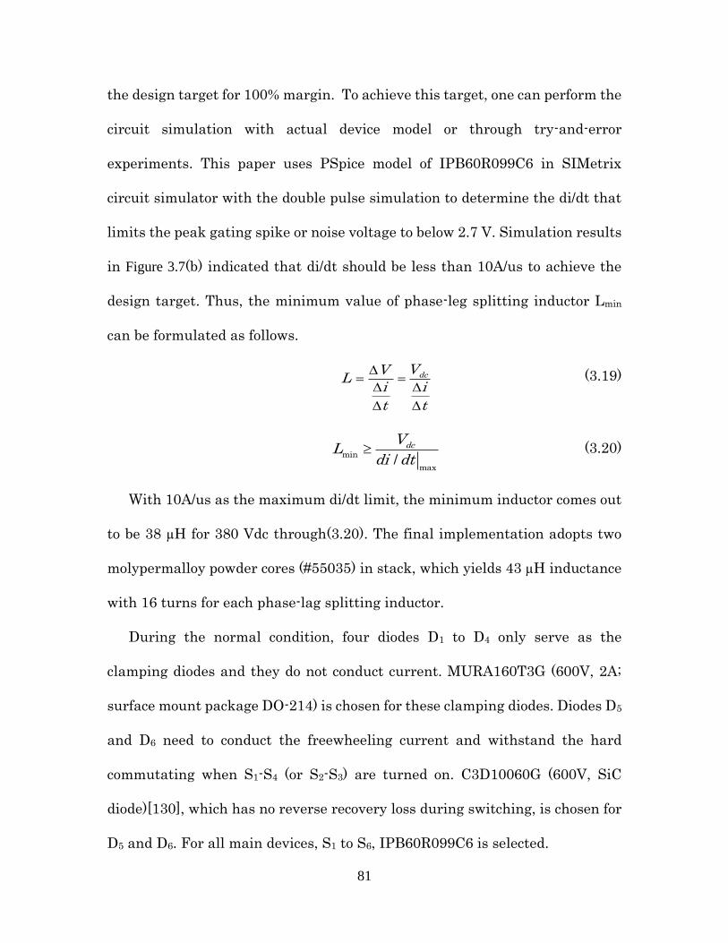
81
the design target for 100% margin. To achieve this target, one can perform the
circuit simulation with actual device model or through try-and-error
experiments. This paper uses PSpice model of IPB60R099C6 in SIMetrix
circuit simulator with the double pulse simulation to determine the di/dt that
limits the peak gating spike or noise voltage to below 2.7 V. Simulation results
in Figure 3.7(b) indicated that di/dt should be less than 10A/us to achieve the
design target. Thus, the minimum value of phase-leg splitting inductor Lmin
can be formulated as follows.
dcVVL
i i
t t
(3.19)
min
max/
dcVL
di dt (3.20)
With 10A/us as the maximum di/dt limit, the minimum inductor comes out
to be 38 µH for 380 Vdc through(3.20). The final implementation adopts two
molypermalloy powder cores (#55035) in stack, which yields 43 µH inductance
with 16 turns for each phase-lag splitting inductor.
During the normal condition, four diodes D1 to D4 only serve as the
clamping diodes and they do not conduct current. MURA160T3G (600V, 2A;
surface mount package DO-214) is chosen for these clamping diodes. Diodes D5
and D6 need to conduct the freewheeling current and withstand the hard
commutating when S1-S4 (or S2-S3) are turned on. C3D10060G (600V, SiC
diode)[130], which has no reverse recovery loss during switching, is chosen for
D5 and D6. For all main devices, S1 to S6, IPB60R099C6 is selected.

82
The losses in the power circuit can be divided into the conduction loss
(power device conduction loss and inductor conduction loss), switching loss,
and inductor core loss.
The voltage drop of MOSFETs can be simplified as a channel resistor, the
voltage drop of diodes can be simplified as a voltage source series with a
channel resistor, which are shown in the flowing respectively.
ds dsv i R (3.21)
ak f akv V i R (3.22)
For the positive half cycle, the duty cycle of S1, S4 can be expressed as (3.23)
. The duty cycle of the MOSFET S5 can be expressed as (3.24). The power losses
on S2, S3, and S6 in the negative half cycle are the same due to the symmetric
operation modes.
1 4
sin( )S Sd m t (3.23)
5
1- sin( )Sd m t (3.24)
Assuming the output current is in-phase with the duty cycle, which means
the pure active generation condition, the output current can be expressed as:
( ) sin( )mi t I t (3.25)
The current in the power device is PWM current, whose conduction time
depends on the duty cycle condition. All the power devices will only work for
half of the line cycle, the conduction losses on high frequency MOSFETs (S1 to
S4), line frequency MOSFETs (S5, S6), and freewheeling Diodes (D5, D6) are
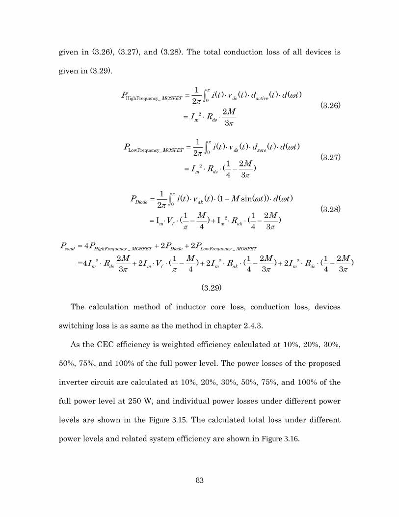
83
given in (3.26), (3.27), and (3.28). The total conduction loss of all devices is
given in (3.29).
HighFrequency_ 0
2
1( ) ( ) ( ) ( )
2
2
3
MOSFET ds active
m ds
P i t v t d t d t
MI R
(3.26)
LowFrequency_ 0
2
1( ) ( ) ( ) ( )
2
1 2( )4 3
MOSFET ds zero
m ds
P i t v t d t d t
MI R
(3.27)
0
2
m m
1( ) ( ) (1 sin( )) ( )
2
1 1 2I ( ) I ( )
4 4 3
Diode ak
f ak
P i t v t M t d t
M MV R
(3.28)
_ _
2 2 2
4 2 2
2 1 1 2 1 2 =4 2 ( ) 2 ( ) 2 ( )
3 4 4 3 4 3
cond HighFrequency MOSFET Diode LowFrequency MOSFET
m ds m f m ak m ds
P P P P
M M M MI R I V I R I R
(3.29)
The calculation method of inductor core loss, conduction loss, devices
switching loss is as same as the method in chapter 2.4.3.
As the CEC efficiency is weighted efficiency calculated at 10%, 20%, 30%,
50%, 75%, and 100% of the full power level. The power losses of the proposed
inverter circuit are calculated at 10%, 20%, 30%, 50%, 75%, and 100% of the
full power level at 250 W, and individual power losses under different power
levels are shown in the Figure 3.15. The calculated total loss under different
power levels and related system efficiency are shown in Figure 3.16.
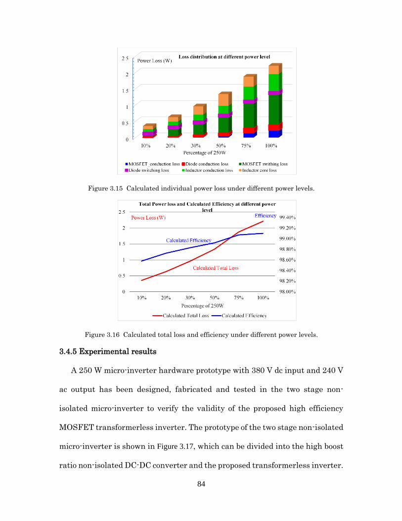
84
Figure 3.15 Calculated individual power loss under different power levels.
Figure 3.16 Calculated total loss and efficiency under different power levels.
3.4.5 Experimental results
A 250 W micro-inverter hardware prototype with 380 V dc input and 240 V
ac output has been designed, fabricated and tested in the two stage non-
isolated micro-inverter to verify the validity of the proposed high efficiency
MOSFET transformerless inverter. The prototype of the two stage non-isolated
micro-inverter is shown in Figure 3.17, which can be divided into the high boost
ratio non-isolated DC-DC converter and the proposed transformerless inverter.
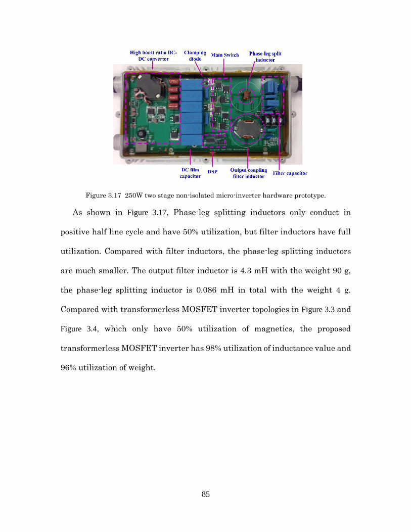
85
Figure 3.17 250W two stage non-isolated micro-inverter hardware prototype.
As shown in Figure 3.17, Phase-leg splitting inductors only conduct in
positive half line cycle and have 50% utilization, but filter inductors have full
utilization. Compared with filter inductors, the phase-leg splitting inductors
are much smaller. The output filter inductor is 4.3 mH with the weight 90 g,
the phase-leg splitting inductor is 0.086 mH in total with the weight 4 g.
Compared with transformerless MOSFET inverter topologies in Figure 3.3 and
Figure 3.4, which only have 50% utilization of magnetics, the proposed
transformerless MOSFET inverter has 98% utilization of inductance value and
96% utilization of weight.
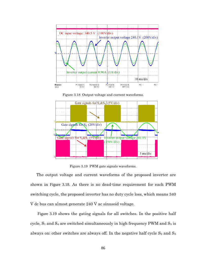
86
Figure 3.18 Output voltage and current waveforms.
Figure 3.19 PWM gate signals waveforms.
The output voltage and current waveforms of the proposed inverter are
shown in Figure 3.18. As there is no dead-time requirement for each PWM
switching cycle, the proposed inverter has no duty cycle loss, which means 340
V dc bus can almost generate 240 V ac sinusoid voltage.
Figure 3.19 shows the gating signals for all switches. In the positive half
cycle, S1 and S4 are switched simultaneously in high frequency PWM and S5 is
always on; other switches are always off. In the negative half cycle S2 and S3
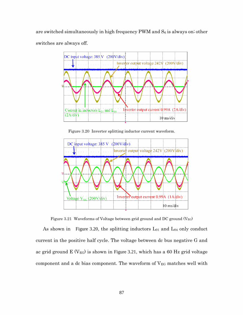
87
are switched simultaneously in high frequency PWM and S6 is always on; other
switches are always off.
Figure 3.20 Inverter splitting inductor current waveform.
Figure 3.21 Waveforms of Voltage between grid ground and DC ground (VEG)
As shown in Figure 3.20, the splitting inductors L01 and L04 only conduct
current in the positive half cycle. The voltage between dc bus negative G and
ac grid ground E (VEG) is shown in Figure 3.21, which has a 60 Hz grid voltage
component and a dc bias component. The waveform of VEG matches well with

88
the calculation results in the (12). This indicates nearly zero high-frequency
voltage on the PV parasitic capacitor, which means minimized leakage current.
Figure 3.22 Efficiency test results of 250W proposed inverter.
In the experiment, YOKOGAWA WT1600 digital power meter is used to
measure voltages, currents, and efficiency [131]. The efficiency measurement
is based on measuring the inverter output ac power and the inverter dc input
power. The efficiency measurement only involves the power stage loss, not
including auxiliary power supply and DSP power losses. The test efficiency
and the calculated efficiency of proposed inverter are shown in Figure 3.22,
which shows 99.01% peak efficiency at full load 250 W. The CEC efficiency is
a weighted efficiency calculated at 10%, 20%, 30%, 50%, 75%, and 100% of
the full power level [25]. The overall CEC efficiency of proposed inverter
power stage is 98.8%, which is calculated through:
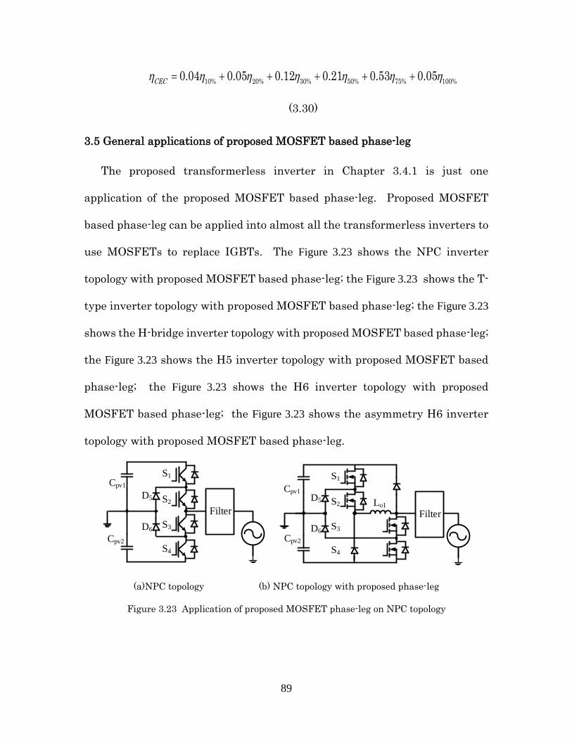
89
10% 20% 30% 50% 75% 100%0.04 0.05 0.12 0.21 0.53 0.05CEC
(3.30)
3.5 General applications of proposed MOSFET based phase-leg
The proposed transformerless inverter in Chapter 3.4.1 is just one
application of the proposed MOSFET based phase-leg. Proposed MOSFET
based phase-leg can be applied into almost all the transformerless inverters to
use MOSFETs to replace IGBTs. The Figure 3.23 shows the NPC inverter
topology with proposed MOSFET based phase-leg; the Figure 3.23 shows the T-
type inverter topology with proposed MOSFET based phase-leg; the Figure 3.23
shows the H-bridge inverter topology with proposed MOSFET based phase-leg;
the Figure 3.23 shows the H5 inverter topology with proposed MOSFET based
phase-leg; the Figure 3.23 shows the H6 inverter topology with proposed
MOSFET based phase-leg; the Figure 3.23 shows the asymmetry H6 inverter
topology with proposed MOSFET based phase-leg.
S1
S2
S3
S4
D5
D6
Cpv1
Cpv2
Filter
S1
S2
S3
S4
D5
D6
Cpv1
Cpv2
Lo1
Filter
(a)NPC topology (b) NPC topology with proposed phase-leg
Figure 3.23 Application of proposed MOSFET phase-leg on NPC topology
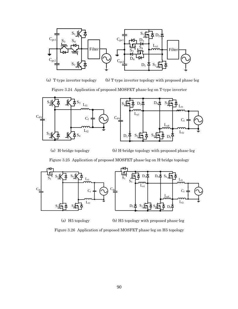
90
S1
S2
S3 S4Cpv1
Cpv2
Filter
S1
S2
S3
S4
Cpv1
Cpv2
Lo1
D1
D2
D4
D3
Filter
(a) T-type inverter topology (b) T-type inverter topology with proposed phase-leg
Figure 3.24 Application of proposed MOSFET phase-leg on T-type inverter
S1
S2 S4
S3
CPV Cf
Lf1
Lf2
CPV Cf
Lf1
Lf2
Lo1
Lo4
S1
S4
S3
D1
D4
D3S2
D2
(a) H-bridge topology (b) H-bridge topology with proposed phase-leg
Figure 3.25 Application of proposed MOSFET phase-leg on H-bridge topology
S1S6
S2 S4
Cdc
S5
Cf
Lf1
Lf2
Lo1
Lo4
S5
S4
S6
D5
D4
D6S2
D2S1
Cdc Cf
Lf1
Lf2
(a) H5 topology (b) H5 topology with proposed phase-leg
Figure 3.26 Application of proposed MOSFET phase-leg on H5 topology
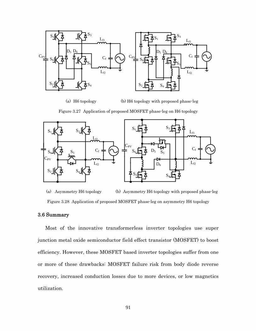
91
S1
S5
S6
D5 D6
S2 S4
S3
CPV Cf
Lf1
Lf2
S1
S5
S6
D5 D6
S2 S4
S3
CPV Cf
Lf1
Lf2
(a) H6 topology (b) H6 topology with proposed phase-leg
Figure 3.27 Application of proposed MOSFET phase-leg on H6 topology
S1
S2 S4
S3
CPV
Cf
Lf1
Lf2
S6 S5
S1
S2 S4
S3
CPVCf
Lf1
Lf2
S6 S5D5
D6
(a) Asymmetry H6 topology (b) Asymmetry H6 topology with proposed phase-leg
Figure 3.28 Application of proposed MOSFET phase-leg on asymmetry H6 topology
3.6 Summary
Most of the innovative transformerless inverter topologies use super
junction metal oxide semiconductor field effect transistor (MOSFET) to boost
efficiency. However, these MOSFET based inverter topologies suffer from one
or more of these drawbacks: MOSFET failure risk from body diode reverse
recovery, increased conduction losses due to more devices, or low magnetics
utilization.

92
With the review of the state-of-the-art low power level MOSFET based
transformerless photovoltaic inverters, the inverter topologies can be divided
into with MOSFET phase-leg and without MOSFET phase-leg. The MOSFET
phase-leg has the issure of body diode reverse recovery, the inverter without
MOSFET phase-leg need to use filter inductor to splide the original MOSFET
phase. Based on these analysis, a novel MOSFET phase-leg method is
proposed.
Based on the proposed phase leg configuration, a high efficiency single-
phase MOSFET transformerless inverter is presented for the PV micro-
inverter applications. The PWM modulation and circuit operation principle are
then described. The common mode and differential mode voltage model is then
presented and analyzed for circuit design. Experimental results of a 250 W
hardware prototype are shown to demonstrate the merits of the proposed
transformerless inverter topology.
The proposed transformeless inverter is just the application of proposed
MOSFET based phase-leg on HERIC inverter. Proposed MOSFET based
phase-leg can be application into almost all the transformerless inverters, and
the application on some typical inverters are shown in the Chapter 3.5, which
will be an interesting research topic for future work.
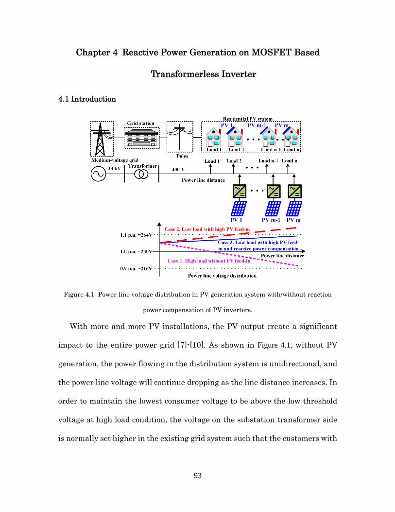
93
Chapter 4 Reactive Power Generation on MOSFET Based
Transformerless Inverter
4.1 Introduction
Figure 4.1 Power line voltage distribution in PV generation system with/without reaction
power compensation of PV inverters.
With more and more PV installations, the PV output create a significant
impact to the entire power grid [7]-[10]. As shown in Figure 4.1, without PV
generation, the power flowing in the distribution system is unidirectional, and
the power line voltage will continue dropping as the line distance increases. In
order to maintain the lowest consumer voltage to be above the low threshold
voltage at high load condition, the voltage on the substation transformer side
is normally set higher in the existing grid system such that the customers with
94
long distance from substation can maintain a reasonable voltage under heavy
load conditions.
Without PV feed-in, the pink dotted line (Case 1) in Figure 4.1 indicates that
the voltage level reduces as the distance increases. With PV generation, the
power flowing in the distribution system can be bi-directional. If a large
number of PV inverters are installed, and significant active power is fed into
grid, the voltage can increase even with long line distance. In some cases, the
customer side voltage may exceed the upper threshold voltage, as shown in red
dashed line (Case 2) of Figure 4.1. One way to resolve this over voltage is to limit
the PV output power, and the other way is to use the cost free PV inverters to
regulate the voltage by absorbing reactive power. The line voltage distribution
of the high PV feed-in with reactive power compensation is described with a
blue solid line (Case 3) in Figure 4.1.
Voltage sags and swells can also happen with unsupported load or sudden
load changes. With reactive power control of PV inverters, the voltage
fluctuations can be mitigated, and system interruption can be avoided.
Avoiding unnecessary interruption implies the improvement of the grid’s
stability, reliability, quality, and efficiency [7]-[10]. In order to fully utilize the
PV inverter capability, IEEE 1547a [29] and The California’s Electric Tariff
Rule 21 [30] are proposing the roles of the distributed energy resource systems
including PV generation. The main requirements of upcoming standards in
USA for PV inverters are summarized as:
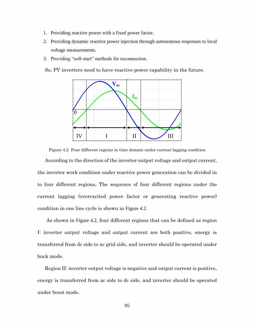
95
1. Providing reactive power with a fixed power factor.
2. Providing dynamic reactive power injection through autonomous responses to local
voltage measurements.
3. Providing “soft-start” methods for reconnection.
So, PV inverters need to have reactive power capability in the future.
Vac
Iac
IV I II III
0
Figure 4.2 Four different regions in time domain under current lagging condition
According to the direction of the inverter output voltage and output current,
the inverter work condition under reactive power generation can be divided in
to four different regions, The sequence of four different regions under the
current lagging (overexcited power factor or generating reactive power)
condition in one line cycle is shown in Figure 4.2.
As shown in Figure 4.2, four different regions that can be defined as region
I: inverter output voltage and output current are both positive, energy is
transferred from dc side to ac grid side, and inverter should be operated under
buck mode.
Region II: inverter output voltage is negative and output current is positive,
energy is transferred from ac side to dc side, and inverter should be operated
under boost mode.

96
Region III: inverter output voltage and output current are both negative,
energy is transferred from dc side to ac grid side, and inverter should be
operated under buck mode.
Region IV: inverter output voltage is positive and output current is negative,
energy is transferred from ac side to dc side, and inverter should be operated
under boost mode.
For the inverter circuit, the bidirectional current flowing capability is
requirement for the reactive power generation.
4.2 Reactive power capability for current MOSFET based transformerless
inverters
For the transformerless inverter topology, some topology use the traditional
complimentary phase-leg method. In this configuration, the high-voltage
MOSFET will suffers from slow reverse recovery of its snappy body diode,
which not only produces high dv/dt, di/dt, and high power loss, but also creates
phase-leg shoot through risk [84]-[89]. Therefore, high-voltage MOSFETs
based phase-leg with top and bottom complimentary devices is not suitable for
hard switching applications. The bidirectional phase-leg with complimentary
MOSFET is shown in Figure 4.3 (a).
Some transformerless inverter topologies are based on the unidirectional
buck method, which is shown in Figure 4.3 (b). In this topology, the snappy body
diode will not conduct current under unidirectional current flowing. The
reverse recovery can be avoided with SiC diode, and high efficiency can be
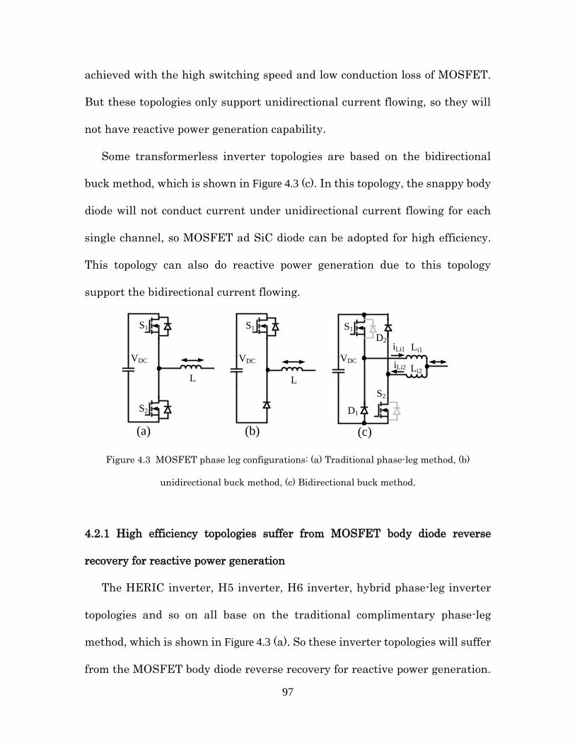
97
achieved with the high switching speed and low conduction loss of MOSFET.
But these topologies only support unidirectional current flowing, so they will
not have reactive power generation capability.
Some transformerless inverter topologies are based on the bidirectional
buck method, which is shown in Figure 4.3 (c). In this topology, the snappy body
diode will not conduct current under unidirectional current flowing for each
single channel, so MOSFET ad SiC diode can be adopted for high efficiency.
This topology can also do reactive power generation due to this topology
support the bidirectional current flowing.
S1
S2
VDC
L
S1
VDC
L
Li1
Li2
S1
D1
S2
D2iLi1
iLi2
VDC
(a) (b) (c)
Figure 4.3 MOSFET phase leg configurations: (a) Traditional phase-leg method, (b)
unidirectional buck method, (c) Bidirectional buck method.
4.2.1 High efficiency topologies suffer from MOSFET body diode reverse
recovery for reactive power generation
The HERIC inverter, H5 inverter, H6 inverter, hybrid phase-leg inverter
topologies and so on all base on the traditional complimentary phase-leg
method, which is shown in Figure 4.3 (a). So these inverter topologies will suffer
from the MOSFET body diode reverse recovery for reactive power generation.
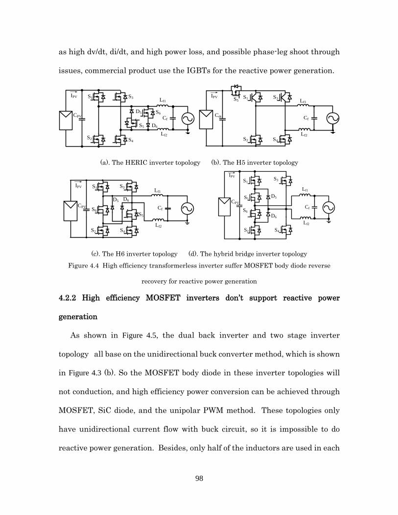
98
as high dv/dt, di/dt, and high power loss, and possible phase-leg shoot through
issues, commercial product use the IGBTs for the reactive power generation.
IPV S1
S5
S6D5
D6
S2 S4
S3
CPV Cf
Lf1
Lf2
S1
S2 S4
S3IPV
Cdc
S5
Cf
Lf1
Lf2
(a). The HERIC inverter topology (b). The H5 inverter topology
IPV S1
S5
S6
D5 D6
S2 S4
S3
CPV Cf
Lf1
Lf2
IPV
S1
S2 S4
S3
CPV
Cf
Lf1
Lf2
S5
S6
D5
D6
(c). The H6 inverter topology (d). The hybrid bridge inverter topology
Figure 4.4 High efficiency transformerless inverter suffer MOSFET body diode reverse
recovery for reactive power generation
4.2.2 High efficiency MOSFET inverters don’t support reactive power
generation
As shown in Figure 4.5, the dual back inverter and two stage inverter
topology all base on the unidirectional buck converter method, which is shown
in Figure 4.3 (b). So the MOSFET body diode in these inverter topologies will
not conduction, and high efficiency power conversion can be achieved through
MOSFET, SiC diode, and the unipolar PWM method. These topologies only
have unidirectional current flow with buck circuit, so it is impossible to do
reactive power generation. Besides, only half of the inductors are used in each
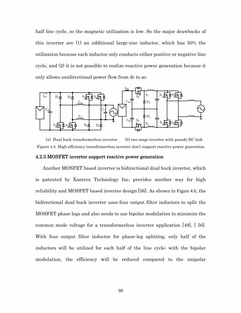
99
half line cycle, so the magnetic utilization is low. So the major drawbacks of
this inverter are (1) an additional large-size inductor, which has 50% the
utilization because each inductor only conducts either positive or negative line
cycle, and (2) it is not possible to realize reactive power generation because it
only allows unidirectional power flow from dc to ac.
Li1
Li2
S1
S4S3D1
D3S2
D2
D4
IPV
Cpv Cf
S1
S2S4
S3
IPV
Cdc1
S5
Cdc2 S6
S1
S4
D1
D2
(a) Dual buck transformerless inverter (b) two stage inverter with pseudo DC link
Figure 4.5 High efficiency transformerless inverter don’t support reactive power generation
4.2.3 MOSFET inverter support reactive power generation
Another MOSFET based inverter is bidirectional dual buck inverter, which
is patented by Xantrex Technology Inc, provides another way for high
reliability and MOSFET based inverter design [56]. As shown in Figure 4.6, the
bidirectional dual buck inverter uses four output filter inductors to split the
MOSFET phase legs and also needs to use bipolar modulation to minimize the
common mode voltage for a transformerless inverter application [49], [ 50].
With four output filter inductor for phase-leg splitting, only half of the
inductors will be utilized for each half of the line cycle; with the bipolar
modulation, the efficiency will be reduced compared to the unipolar
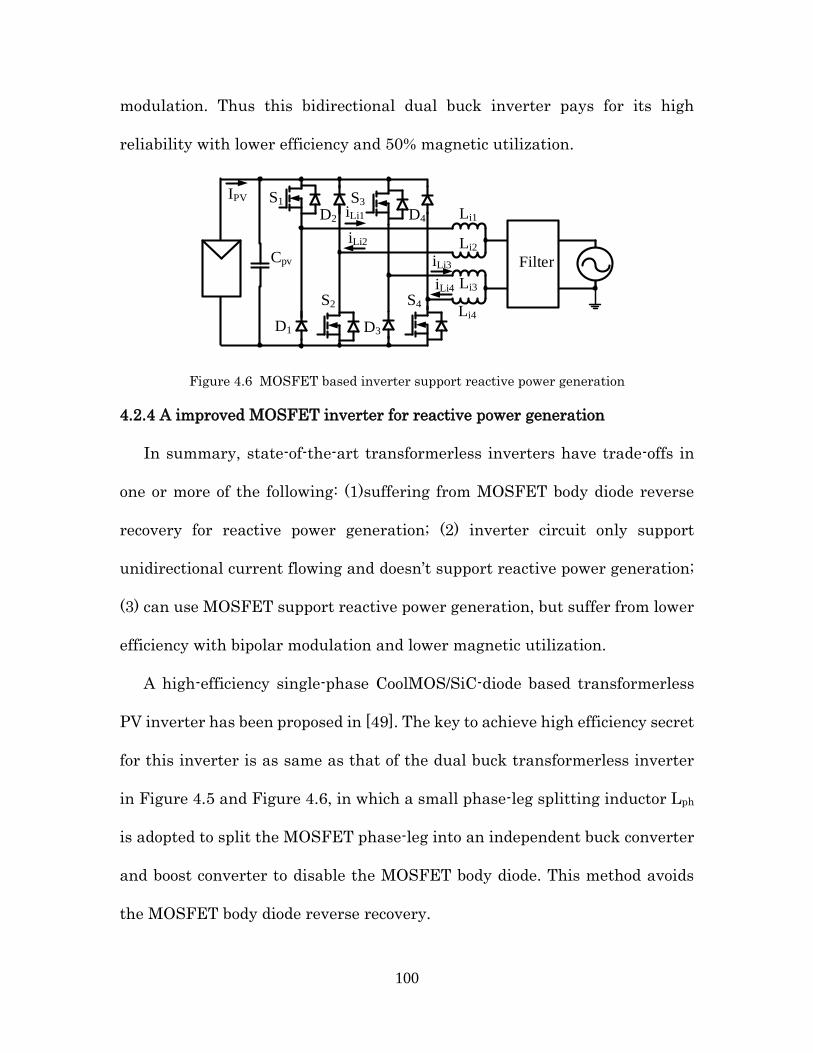
100
modulation. Thus this bidirectional dual buck inverter pays for its high
reliability with lower efficiency and 50% magnetic utilization.
Li1
Li2
Li3
Li4
S1
S4
S3
D1
D4
D3
S2
D2iLi1
iLi2
IPV
Cpv FilteriLi3
iLi4
Figure 4.6 MOSFET based inverter support reactive power generation
4.2.4 A improved MOSFET inverter for reactive power generation
In summary, state-of-the-art transformerless inverters have trade-offs in
one or more of the following: (1)suffering from MOSFET body diode reverse
recovery for reactive power generation; (2) inverter circuit only support
unidirectional current flowing and doesn’t support reactive power generation;
(3) can use MOSFET support reactive power generation, but suffer from lower
efficiency with bipolar modulation and lower magnetic utilization.
A high-efficiency single-phase CoolMOS/SiC-diode based transformerless
PV inverter has been proposed in [49]. The key to achieve high efficiency secret
for this inverter is as same as that of the dual buck transformerless inverter
in Figure 4.5 and Figure 4.6, in which a small phase-leg splitting inductor Lph
is adopted to split the MOSFET phase-leg into an independent buck converter
and boost converter to disable the MOSFET body diode. This method avoids
the MOSFET body diode reverse recovery.
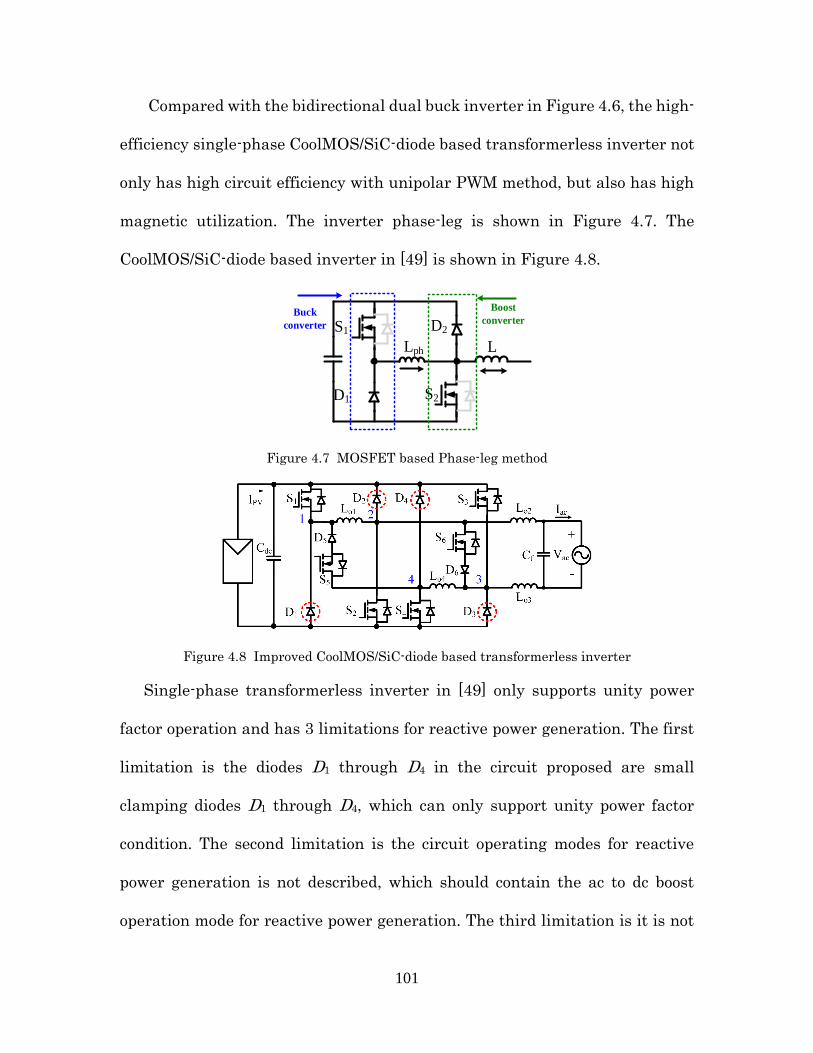
101
Compared with the bidirectional dual buck inverter in Figure 4.6, the high-
efficiency single-phase CoolMOS/SiC-diode based transformerless inverter not
only has high circuit efficiency with unipolar PWM method, but also has high
magnetic utilization. The inverter phase-leg is shown in Figure 4.7. The
CoolMOS/SiC-diode based inverter in [49] is shown in Figure 4.8.
L
S1
S2
D2
D1
Lph
Buck
converter
Boost
converter
Figure 4.7 MOSFET based Phase-leg method
Figure 4.8 Improved CoolMOS/SiC-diode based transformerless inverter
Single-phase transformerless inverter in [49] only supports unity power
factor operation and has 3 limitations for reactive power generation. The first
limitation is the diodes D1 through D4 in the circuit proposed are small
clamping diodes D1 through D4, which can only support unity power factor
condition. The second limitation is the circuit operating modes for reactive
power generation is not described, which should contain the ac to dc boost
operation mode for reactive power generation. The third limitation is it is not

102
capable of reactive power generation with the PWM modulation method
proposed in [49], or the traditional unipolar or bipolar modulation method.
The first limitation of the circuit proposed in [49] is the use of small
clamping diodes D1 through D4, which can only support unity power factor
condition (clamping diodes don’t conduct current, are not power diode). In this
paper, these clamping diodes are replaced with Schottky power diodes and will
conduct current when energy is transferred from ac grid side to dc side. As
shown in Figure 4.8, with the using of Schottky diodes, the improved circuit
would allow non-unity power factor power flowing.
4.3 Operating modes of the improved MOSFET based transformerless
inverters
The second limitation of the improved single-phase CoolMOS/SiC-diode
based transformerless inverter is the circuit operating modes for reactive
power generation is not described, which should contain the ac to dc boost
operation mode for reactive power generation. Based on the analysis in chapter
4.1, four different inverter circuit operating modes for four different regions
will be proposed in this part.
When the grid voltage and the inverter output current are both positive,
the inverter works in region I. The inverter circuit will be operated in buck
mode with S1, S4 and S5. S1 and S4 switch simultaneously in high frequency;
S5 remains on during this region. The inverter circuit operating mode is shown
in Figure 4.9. As shown in Figure 4.9 (a), when S1 and S4 are turned on, D5 will
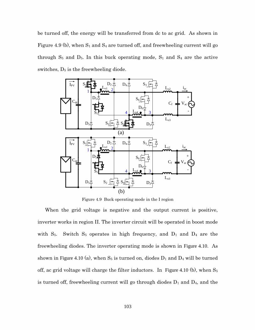
103
be turned off, the energy will be transferred from dc to ac grid. As shown in
Figure 4.9 (b), when S1 and S4 are turned off, and freewheeling current will go
through S5 and D5. In this buck operating mode, S1 and S4 are the active
switches, D5 is the freewheeling diode.
Lo1
Lo4
S1
S4
S3
D1
D4
D3S2
D2
S5
S6D5
D6
IPV
Cdc
1 2
34
Lo1
Lo4
S1
S4
S3
D1
D4
D3S2
D2
S5
S6D5
D6
IPV
Cdc
1 2
34
(a)
(b)
iac
Vac
Lo2
Lo3
+
-
Cf
iac
Vac
Lo2
Lo3
+
-
Cf
Figure 4.9 Buck operating mode in the I region
When the grid voltage is negative and the output current is positive,
inverter works in region II. The inverter circuit will be operated in boost mode
with S5. Switch S5 operates in high frequency, and D1 and D4 are the
freewheeling diodes. The inverter operating mode is shown in Figure 4.10. As
shown in Figure 4.10 (a), when S5 is turned on, diodes D1 and D4 will be turned
off, ac grid voltage will charge the filter inductors. In Figure 4.10 (b), when S5
is turned off, freewheeling current will go through diodes D1 and D4, and the
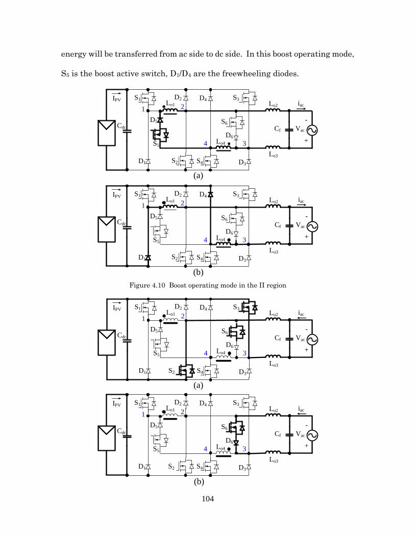
104
energy will be transferred from ac side to dc side. In this boost operating mode,
S5 is the boost active switch, D1/D4 are the freewheeling diodes.
Lo1
Lo4
S1
S4
S3
D1
D4
D3S2
D2
S5
S6D5
D6
IPV
Cdc
1 2
34
Lo1
Lo4
S1
S4
S3
D1
D4
D3S2
D2
S5
S6D5
D6
IPV
Cdc
1 2
34
(a)
(b)
iac
Vac
Lo2
Lo3
+
-
Cf
iac
Vac
Lo2
Lo3
+
-
Cf
Figure 4.10 Boost operating mode in the II region
Lo1
Lo4
S1
S4
S3
D1
D4
D3S2
D2
S5
S6D5
D6
IPV
Cdc
1 2
34
Lo1
Lo4
S1
S4
S3
D1
D4
D3S2
D2
S5
S6D5
D6
IPV
Cdc
1 2
34
(a)
(b)
iac
Vac
Lo2
Lo3
+
-
Cf
iac
Vac
Lo2
Lo3
+
-
Cf
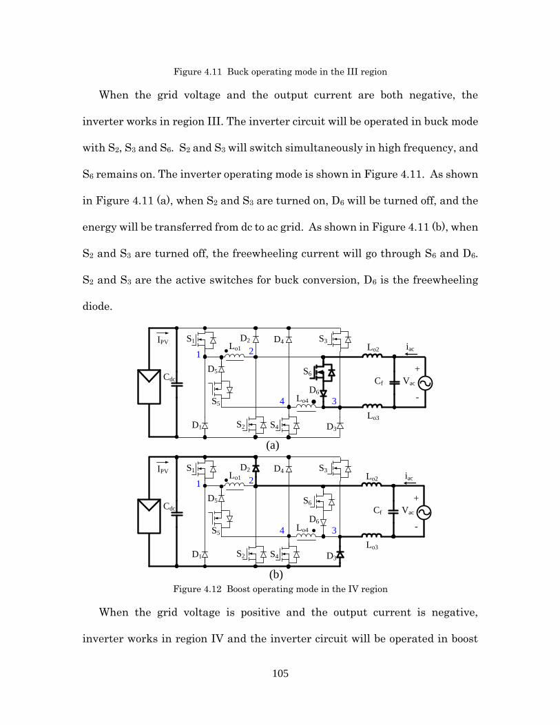
105
Figure 4.11 Buck operating mode in the III region
When the grid voltage and the output current are both negative, the
inverter works in region III. The inverter circuit will be operated in buck mode
with S2, S3 and S6. S2 and S3 will switch simultaneously in high frequency, and
S6 remains on. The inverter operating mode is shown in Figure 4.11. As shown
in Figure 4.11 (a), when S2 and S3 are turned on, D6 will be turned off, and the
energy will be transferred from dc to ac grid. As shown in Figure 4.11 (b), when
S2 and S3 are turned off, the freewheeling current will go through S6 and D6.
S2 and S3 are the active switches for buck conversion, D6 is the freewheeling
diode.
Lo1
Lo4
S1
S4
S3
D1
D4
D3S2
D2
S5
S6D5
D6
IPV
Cdc
1 2
34
Lo1
Lo4
S1
S4
S3
D1
D4
D3S2
D2
S5
S6D5
D6
IPV
Cdc
1 2
34
(a)
(b)
iac
Vac
Lo2
Lo3
+
-
Cf
iac
Vac
Lo2
Lo3
+
-
Cf
Figure 4.12 Boost operating mode in the IV region
When the grid voltage is positive and the output current is negative,
inverter works in region IV and the inverter circuit will be operated in boost
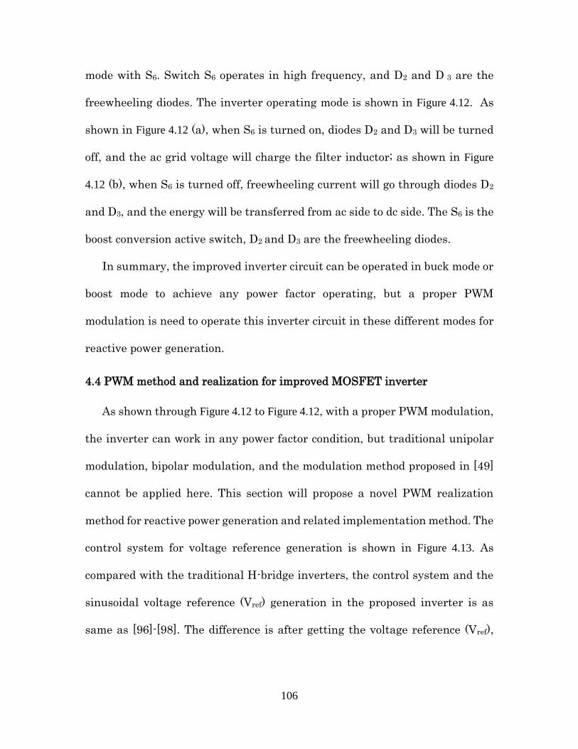
106
mode with S6. Switch S6 operates in high frequency, and D2 and D 3 are the
freewheeling diodes. The inverter operating mode is shown in Figure 4.12. As
shown in Figure 4.12 (a), when S6 is turned on, diodes D2 and D3 will be turned
off, and the ac grid voltage will charge the filter inductor; as shown in Figure
4.12 (b), when S6 is turned off, freewheeling current will go through diodes D2
and D3, and the energy will be transferred from ac side to dc side. The S6 is the
boost conversion active switch, D2 and D3 are the freewheeling diodes.
In summary, the improved inverter circuit can be operated in buck mode or
boost mode to achieve any power factor operating, but a proper PWM
modulation is need to operate this inverter circuit in these different modes for
reactive power generation.
4.4 PWM method and realization for improved MOSFET inverter
As shown through Figure 4.12 to Figure 4.12, with a proper PWM modulation,
the inverter can work in any power factor condition, but traditional unipolar
modulation, bipolar modulation, and the modulation method proposed in [49]
cannot be applied here. This section will propose a novel PWM realization
method for reactive power generation and related implementation method. The
control system for voltage reference generation is shown in Figure 4.13. As
compared with the traditional H-bridge inverters, the control system and the
sinusoidal voltage reference (Vref) generation in the proposed inverter is as
same as [96]-[98]. The difference is after getting the voltage reference (Vref),
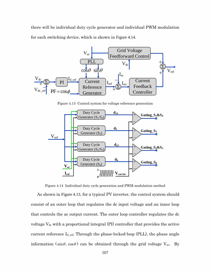
107
there will be individual duty cycle generator and individual PWM modulation
for each switching device, which is shown in Figure 4.14.
Current
Feedback
Controller
Iref Ierr
Iac
Vdc
Vdc_ref
PI
Vac
PLL
Id_ref
sincos
Current
Reference
GeneratorPF cos
Grid Voltage
Feedforward Control
Vref
Vdc
Figure 4.13 Control system for voltage reference generation
Vcarrier
Gating_S1&S4
d14Duty Cycle
Generator (S1/S4)
Gating_S5
d5Duty Cycle
Generator (S5)
Gating_S2&S3
d23Duty Cycle
Generator (S2/S3)
Gating_S6
d6Duty Cycle
Generator (S6)
1
0
Iref
Vac
Vref
Figure 4.14 Individual duty cycle generation and PWM modulation method
As shown in Figure 4.13, for a typical PV inverter, the control system should
consist of an outer loop that regulates the dc input voltage and an inner loop
that controls the ac output current. The outer loop controller regulates the dc
voltage Vdc with a proportional-integral (PI) controller that provides the active
current reference Id_ref. Through the phase-locked-loop (PLL), the phase angle
information ( sin , cos ) can be obtained through the grid voltage Vac. By

108
combining the active current reference and power factor command cos, a
sinusoidal current reference Iref can be generated through the current reference
generator module. Together with grid voltage feedforward control loop and the
grid current feedback controller, a sinusoidal voltage reference (Vref) can then
be generated for duty cycle generation and PWM modulation.
As shown in Figure 4.14, proposed PWM method has an individual duty cycle
generator and PWM modulation module for each pair of switches. The switches
S1 and S4 obtain their duty cycle reference d14 through a duty cycle generator
(S1/S4), which will let inverter to be operated in buck mode in the I region (refer
to Figure 4.14), and the duty cycle of the S1 and S4 is,
1 4 refd d V (4.1)
The Switches S5 obtain the duty cycle reference d5 through a duty cycle
generator (S5), which will let inverter to be operated in buck mode in the I
region and the boost mode in the II region (refer to Figure 4.14). The S5 will be
constant on in I region, and the duty cycle of S5 for the II region is:
51 refd V (4.2)
The switches S2 and S3 obtain their duty cycle reference d23 through a duty
cycle generator (S2/S3), which will let inverter to be operated in buck mode in
the III region (refer to Figure 4.14), and the duty cycle of S2 and S3 is:
2 3 refd d V (4.3)
The Switches S6 obtain the duty cycle reference d6 through a duty cycle
generator (S6), which will let inverter to be operated in buck mode in the III
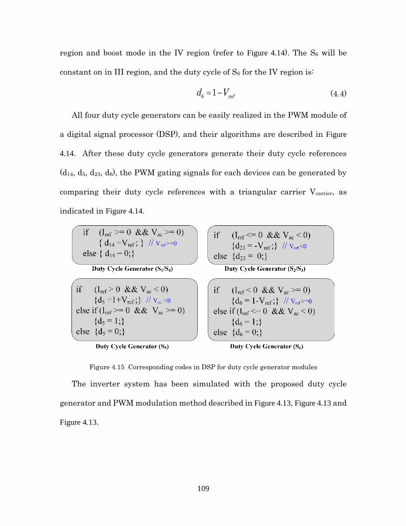
109
region and boost mode in the IV region (refer to Figure 4.14). The S6 will be
constant on in III region, and the duty cycle of S6 for the IV region is:
61 refd V (4.4)
All four duty cycle generators can be easily realized in the PWM module of
a digital signal processor (DSP), and their algorithms are described in Figure
4.14. After these duty cycle generators generate their duty cycle references
(d14, d5, d23, d6), the PWM gating signals for each devices can be generated by
comparing their duty cycle references with a triangular carrier Vcarrier, as
indicated in Figure 4.14.
Figure 4.15 Corresponding codes in DSP for duty cycle generator modules
The inverter system has been simulated with the proposed duty cycle
generator and PWM modulation method described in Figure 4.13, Figure 4.13 and
Figure 4.13.

110
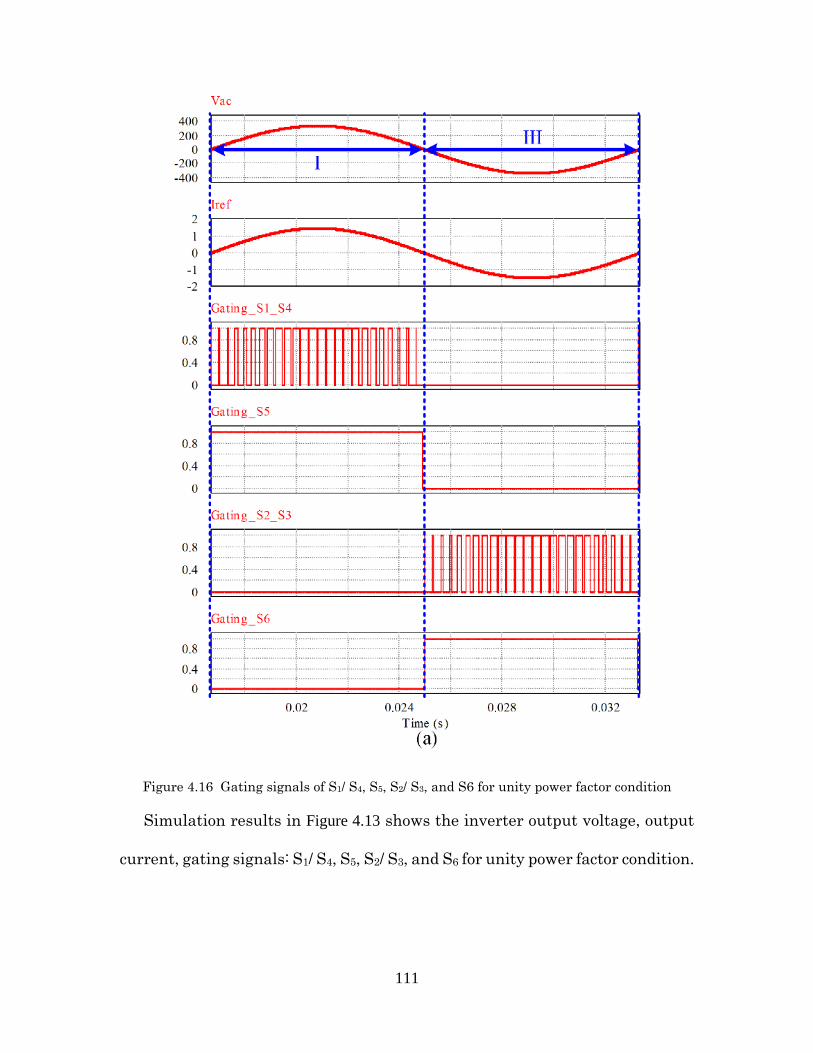
111
Figure 4.16 Gating signals of S1/ S4, S5, S2/ S3, and S6 for unity power factor condition
Simulation results in Figure 4.13 shows the inverter output voltage, output
current, gating signals: S1/ S4, S5, S2/ S3, and S6 for unity power factor condition.
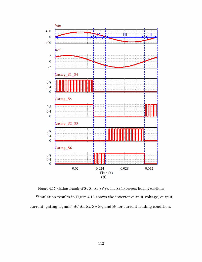
112
Figure 4.17 Gating signals of S1/ S4, S5, S2/ S3, and S6 for current leading condition
Simulation results in Figure 4.13 shows the inverter output voltage, output
current, gating signals: S1/ S4, S5, S2/ S3, and S6 for current leading condition.
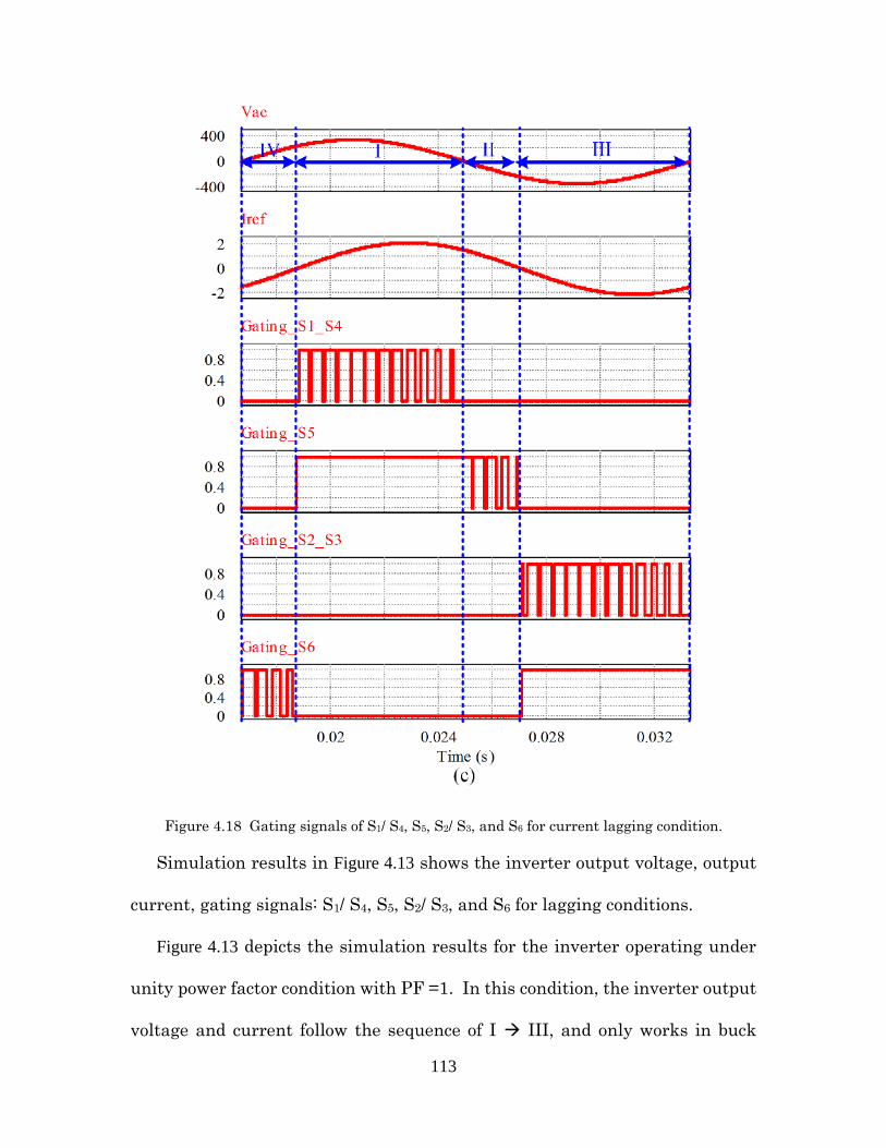
113
Figure 4.18 Gating signals of S1/ S4, S5, S2/ S3, and S6 for current lagging condition.
Simulation results in Figure 4.13 shows the inverter output voltage, output
current, gating signals: S1/ S4, S5, S2/ S3, and S6 for lagging conditions.
Figure 4.13 depicts the simulation results for the inverter operating under
unity power factor condition with PF =1. In this condition, the inverter output
voltage and current follow the sequence of I III, and only works in buck
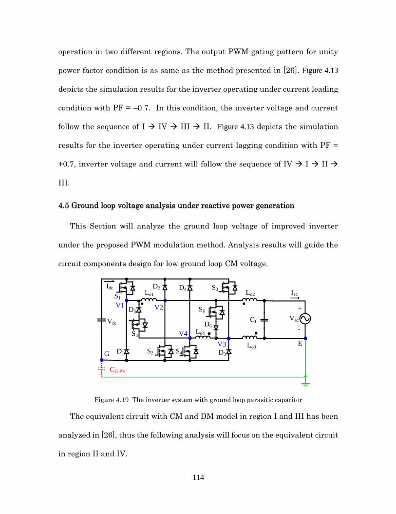
114
operation in two different regions. The output PWM gating pattern for unity
power factor condition is as same as the method presented in [26]. Figure 4.13
depicts the simulation results for the inverter operating under current leading
condition with PF = –0.7. In this condition, the inverter voltage and current
follow the sequence of I IV III II. Figure 4.13 depicts the simulation
results for the inverter operating under current lagging condition with PF =
+0.7, inverter voltage and current will follow the sequence of IV I II
III.
4.5 Ground loop voltage analysis under reactive power generation
This Section will analyze the ground loop voltage of improved inverter
under the proposed PWM modulation method. Analysis results will guide the
circuit components design for low ground loop CM voltage.
Lo1 Iac
Vac
Lo2
Lo3
Lo4
S1
S4
S3
D1
D4
D3S2
D2
S5
S6D5
D6
Idc
Vdc
G
E
+
-
V1 V2
V3
V4
CG-PV
Cf
Figure 4.19 The inverter system with ground loop parasitic capacitor
The equivalent circuit with CM and DM model in region I and III has been
analyzed in [26], thus the following analysis will focus on the equivalent circuit
in region II and IV.
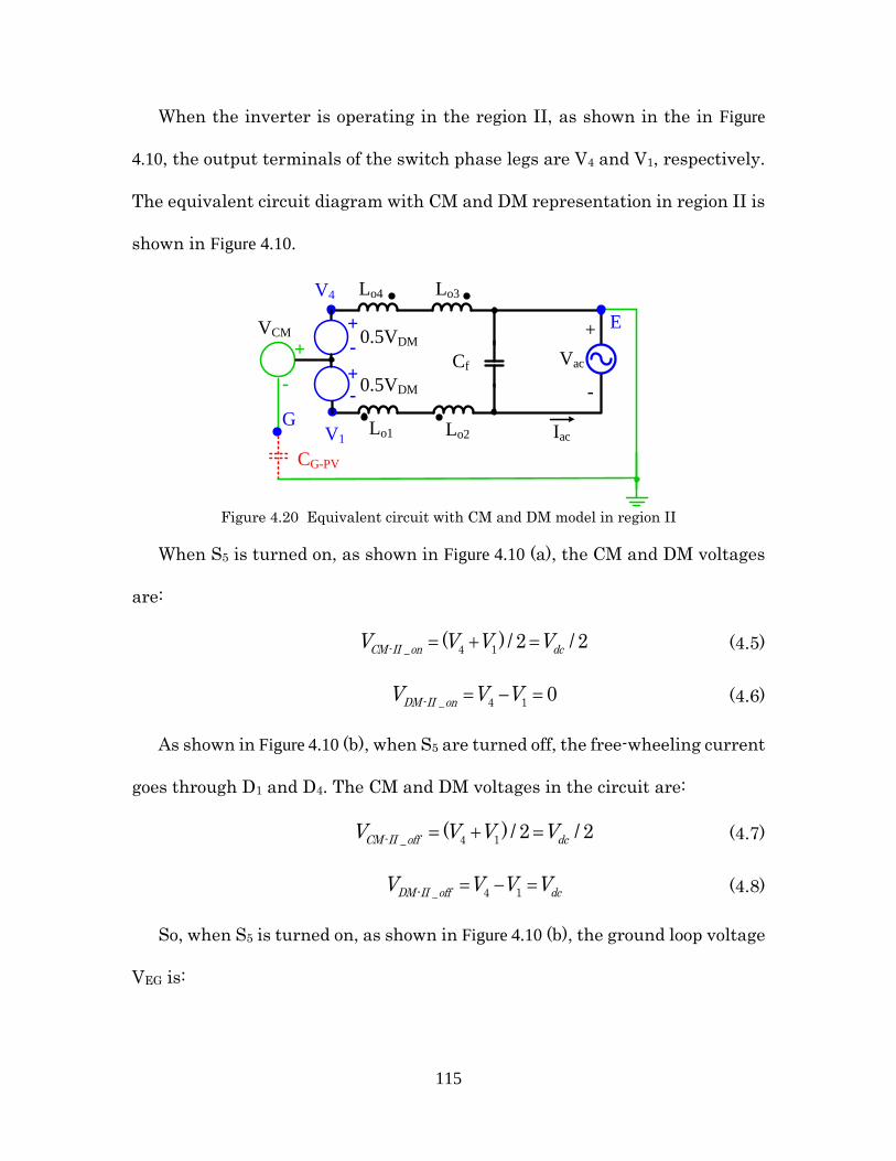
115
When the inverter is operating in the region II, as shown in the in Figure
4.10, the output terminals of the switch phase legs are V4 and V1, respectively.
The equivalent circuit diagram with CM and DM representation in region II is
shown in Figure 4.10.
Vac
Lo2
Lo3
E+
-
V4 Lo4
V1Lo1
CG-PV
G
0.5VDM
0.5VDM
VCM
-+
+
-+
-
Cf
Iac
Figure 4.20 Equivalent circuit with CM and DM model in region II
When S5 is turned on, as shown in Figure 4.10 (a), the CM and DM voltages
are:
- _ 4 1( ) / 2 / 2CM II on dcV V V V (4.5)
- _ 4 10DM II onV V V (4.6)
As shown in Figure 4.10 (b), when S5 are turned off, the free-wheeling current
goes through D1 and D4. The CM and DM voltages in the circuit are:
- _ 4 1( ) / 2 / 2CM II off dcV V V V (4.7)
- _ 4 1DM II off dcV V V V (4.8)
So, when S5 is turned on, as shown in Figure 4.10 (b), the ground loop voltage
VEG is:
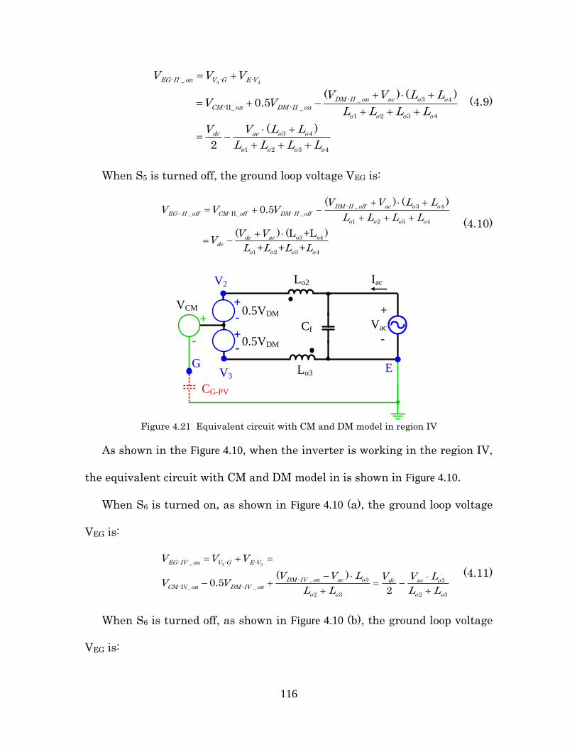
116
4 4- _ - -
- _ 3 4
-II_ - _
1 2 3 4
3 4
1 2 3 4
( ) ( )0.5
( )
2
EG II on V G E V
DM II on ac o o
CM on DM II on
o o o o
dc ac o o
o o o o
V V V
V V L LV V
L L L L
V V L L
L L L L
(4.9)
When S5 is turned off, the ground loop voltage VEG is:
- _ 3 4
_ -II_ - _
1 2 3 4
o3 o4
1 2 3 4
( ) ( )0.5
( ) (L +L )
+ + +
DM II off ac o o
EG II off CM off DM II off
o o o o
dc acdc
o o o o
V V L LV V V
L L L L
V VV
L L L L
(4.10)
Vac
Lo2
Lo3 E
+
-
V2
V3
CG-PV
G
0.5VDM
0.5VDM
VCM
-+
+
-+
-
Cf
Iac
Figure 4.21 Equivalent circuit with CM and DM model in region IV
As shown in the Figure 4.10, when the inverter is working in the region IV,
the equivalent circuit with CM and DM model in is shown in Figure 4.10.
When S6 is turned on, as shown in Figure 4.10 (a), the ground loop voltage
VEG is:
3 3- _ - -
- _ 3 3-IV_ - _
2 3 2 3
( )0.5
2
EG IV on V G E V
DM IV on ac o dc ac oCM on DM IV on
o o o o
V V V
V V L V V LV V
L L L L
(4.11)
When S6 is turned off, as shown in Figure 4.10 (b), the ground loop voltage
VEG is:
117
- _ 3
_ -IV_ - _
2 3
3
2 3
( )0.5
( )
DM IV off ac o
EG IV off CM off DM IV off
o o
dc ac o
o o
V V LV V V
L L
V V L
L L
(4.12)
In the inverter, if the inductances of Lo2 and Lo3 have the same value, and
Lo1 and Lo4 values are equal, the ground loop voltage VEG comes out to be the
same in different operating modes according to analysis results in[49] and
(3.9), (3.10), (3.11), and (3.12).
- _ _ - _ _
- _ _ - _ _2
EG I on EG I off EG II on EG II off
dc acEG III on EG III off EG IV on EG IV off
V V V V
V VV V V V
(4.13)
With proposed PWM modulation method, if the inductors (Lo1 and Lo4) or
inductors (Lo2 and Lo3) are not designed to have similar inductance, the DM
and CM voltages will have high-frequency components in the ground loop
voltage VEG, which will result in high-frequency ground loop leakage current.
In order to minimize this high frequency leakage current, Lo2 and Lo3 are better
to be designed with same value. Similarly, Lo1 and Lo4 are also better to be
designed with same value. With this inductor value match, the ground loop
voltage VEG will be a line-frequency sinusoidal voltage with a dc offset, which
is shown in (19). In the hardware, Lo2 and Lo3 are coupled together, Lo1 and Lo4
are also coupled together, and the experimental waveform of VEG will be shown
in Section V to verify the validity of the analysis in this section.
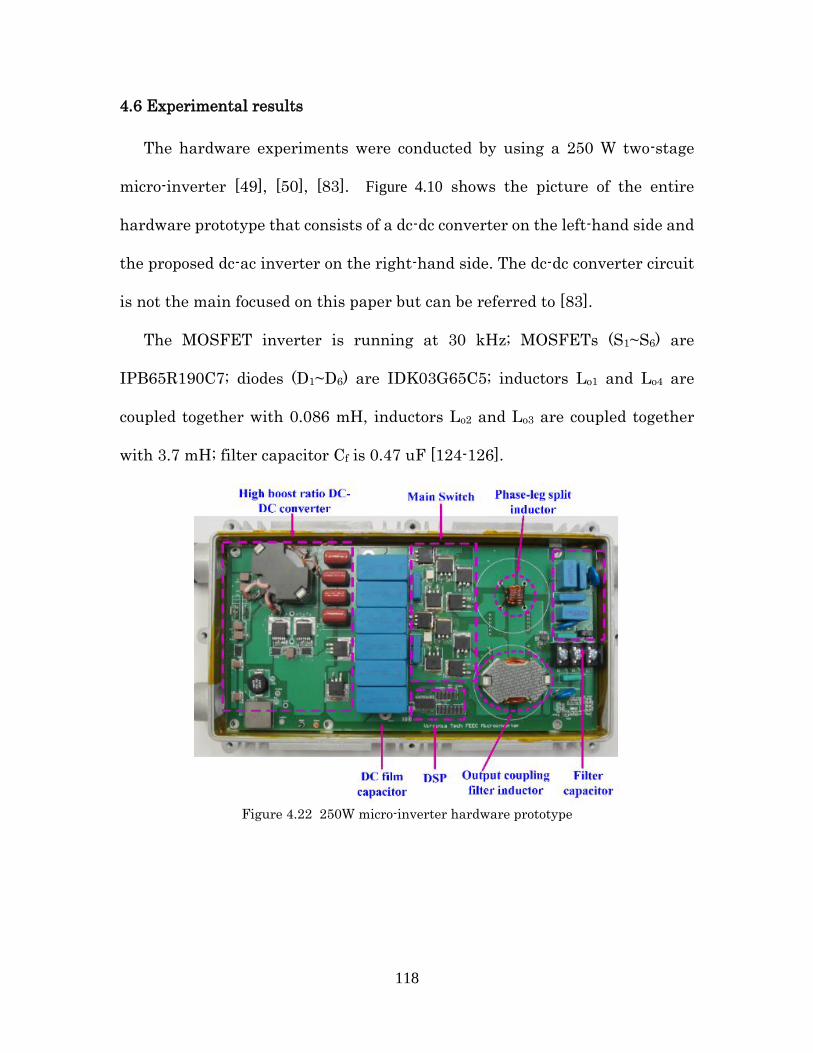
118
4.6 Experimental results
The hardware experiments were conducted by using a 250 W two-stage
micro-inverter [49], [50], [83]. Figure 4.10 shows the picture of the entire
hardware prototype that consists of a dc-dc converter on the left-hand side and
the proposed dc-ac inverter on the right-hand side. The dc-dc converter circuit
is not the main focused on this paper but can be referred to [83].
The MOSFET inverter is running at 30 kHz; MOSFETs (S1~S6) are
IPB65R190C7; diodes (D1~D6) are IDK03G65C5; inductors Lo1 and Lo4 are
coupled together with 0.086 mH, inductors Lo2 and Lo3 are coupled together
with 3.7 mH; filter capacitor Cf is 0.47 uF [124-126].
Figure 4.22 250W micro-inverter hardware prototype
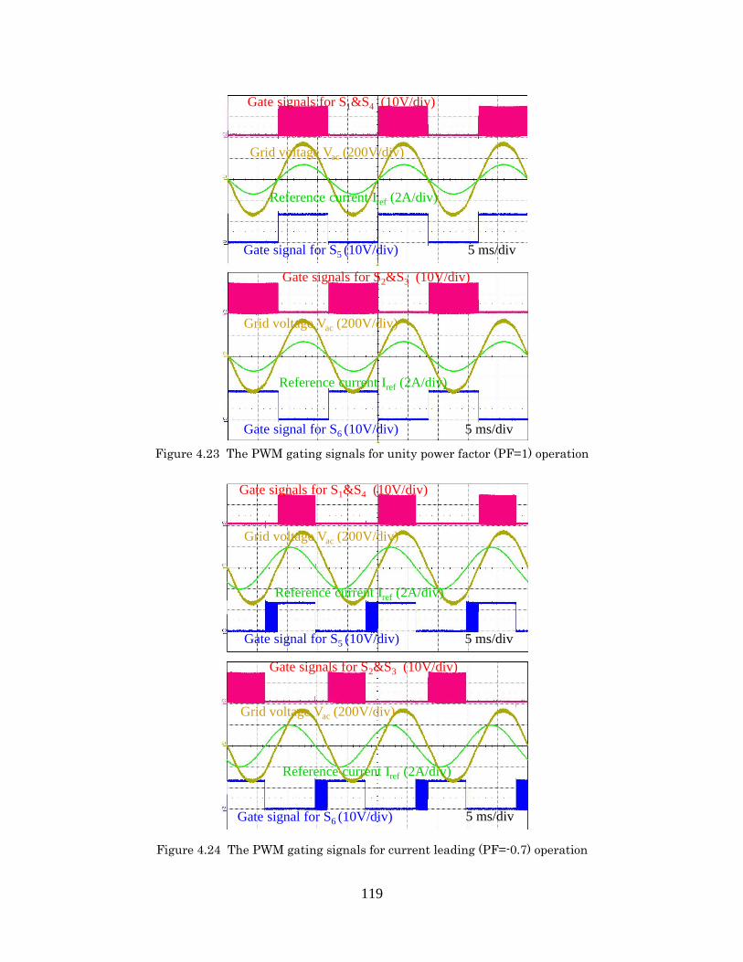
119
Gate signals for S1&S4 (10V/div)
Gate signal for S5 (10V/div)
Grid voltage Vac (200V/div)
Reference current Iref (2A/div)
Re
5 ms/div
Gate signals for S2&S3 (10V/div)
Gate signal for S6 (10V/div)
Grid voltage Vac (200V/div)
Reference current Iref (2A/div)
Re
5 ms/div
Figure 4.23 The PWM gating signals for unity power factor (PF=1) operation
Gate signals for S1&S4 (10V/div)
Gate signal for S5 (10V/div)
Grid voltage Vac (200V/div)
Reference current Iref (2A/div)
Re
5 ms/div
Gate signals for S2&S3 (10V/div)
Gate signal for S6 (10V/div)
Grid voltage Vac (200V/div)
Reference current Iref (2A/div)
Re
5 ms/div
Figure 4.24 The PWM gating signals for current leading (PF=-0.7) operation
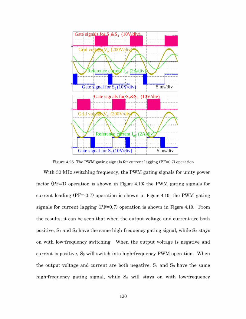
120
Gate signals for S1&S4 (10V/div)
Gate signal for S5 (10V/div)
Grid voltage Vac (200V/div)
Reference current Iref (2A/div)
Re
5 ms/div
Gate signals for S2&S3 (10V/div)
Gate signal for S6 (10V/div)
Grid voltage Vac (200V/div)
Reference current Iref (2A/div)
Re
5 ms/div
Figure 4.25 The PWM gating signals for current lagging (PF=0.7) operation
With 30-kHz switching frequency, the PWM gating signals for unity power
factor (PF=1) operation is shown in Figure 4.10; the PWM gating signals for
current leading (PF=-0.7) operation is shown in Figure 4.10; the PWM gating
signals for current lagging (PF=0.7) operation is shown in Figure 4.10. From
the results, it can be seen that when the output voltage and current are both
positive, S1 and S4 have the same high-frequency gating signal, while S5 stays
on with low-frequency switching. When the output voltage is negative and
current is positive, S5 will switch into high-frequency PWM operation. When
the output voltage and current are both negative, S2 and S3 have the same
high-frequency gating signal, while S6 will stays on with low-frequency
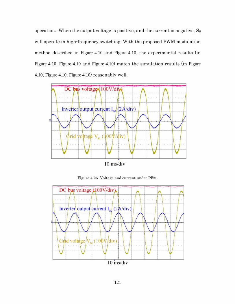
121
operation. When the output voltage is positive, and the current is negative, S6
will operate in high-frequency switching. With the proposed PWM modulation
method described in Figure 4.10 and Figure 4.10, the experimental results (in
Figure 4.10, Figure 4.10 and Figure 4.10) match the simulation results (in Figure
4.10, Figure 4.10, Figure 4.10) reasonably well.
Figure 4.26 Voltage and current under PF=1
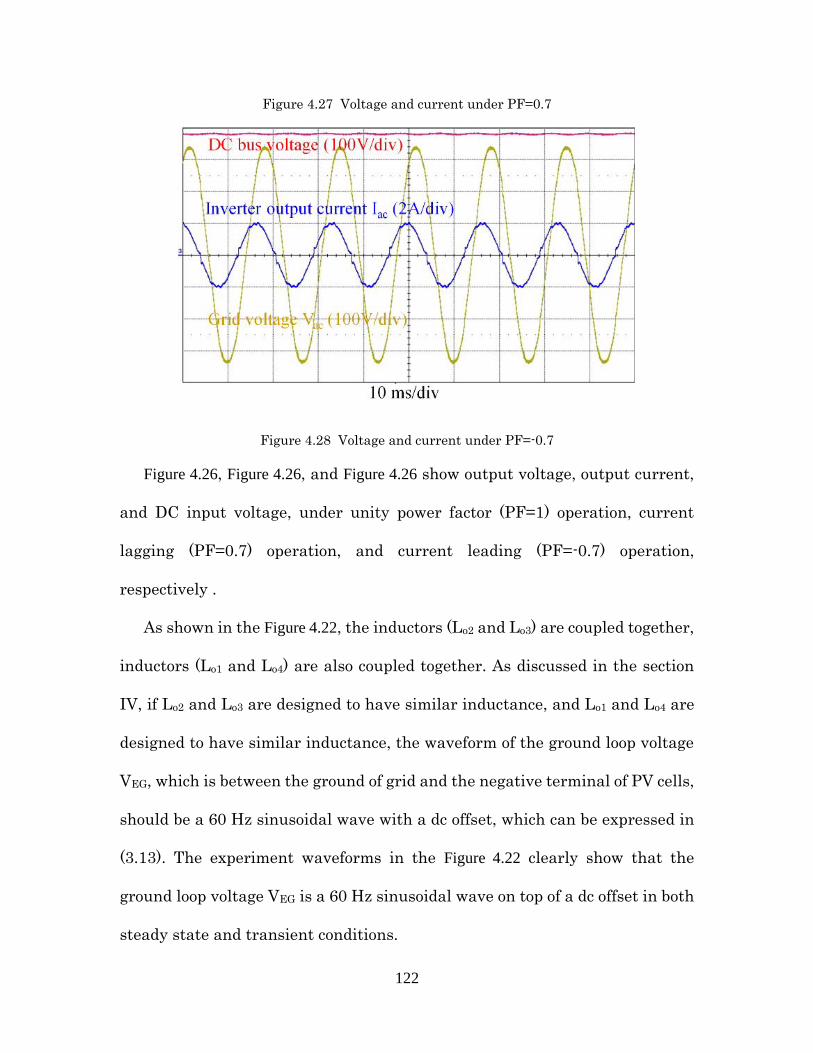
122
Figure 4.27 Voltage and current under PF=0.7
Figure 4.28 Voltage and current under PF=-0.7
Figure 4.26, Figure 4.26, and Figure 4.26 show output voltage, output current,
and DC input voltage, under unity power factor (PF=1) operation, current
lagging (PF=0.7) operation, and current leading (PF=-0.7) operation,
respectively .
As shown in the Figure 4.22, the inductors (Lo2 and Lo3) are coupled together,
inductors (Lo1 and Lo4) are also coupled together. As discussed in the section
IV, if Lo2 and Lo3 are designed to have similar inductance, and Lo1 and Lo4 are
designed to have similar inductance, the waveform of the ground loop voltage
VEG, which is between the ground of grid and the negative terminal of PV cells,
should be a 60 Hz sinusoidal wave with a dc offset, which can be expressed in
(3.13). The experiment waveforms in the Figure 4.22 clearly show that the
ground loop voltage VEG is a 60 Hz sinusoidal wave on top of a dc offset in both
steady state and transient conditions.
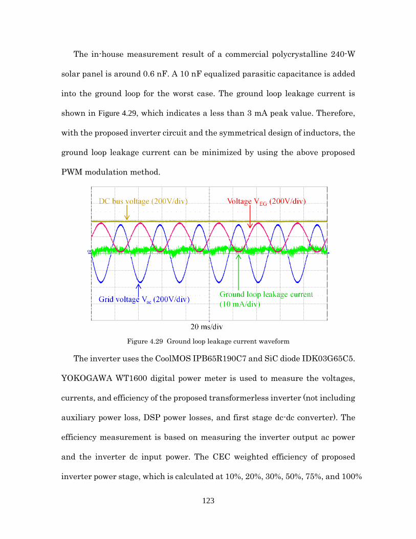
123
The in-house measurement result of a commercial polycrystalline 240-W
solar panel is around 0.6 nF. A 10 nF equalized parasitic capacitance is added
into the ground loop for the worst case. The ground loop leakage current is
shown in Figure 4.29, which indicates a less than 3 mA peak value. Therefore,
with the proposed inverter circuit and the symmetrical design of inductors, the
ground loop leakage current can be minimized by using the above proposed
PWM modulation method.
Figure 4.29 Ground loop leakage current waveform
The inverter uses the CoolMOS IPB65R190C7 and SiC diode IDK03G65C5.
YOKOGAWA WT1600 digital power meter is used to measure the voltages,
currents, and efficiency of the proposed transformerless inverter (not including
auxiliary power loss, DSP power losses, and first stage dc-dc converter). The
efficiency measurement is based on measuring the inverter output ac power
and the inverter dc input power. The CEC weighted efficiency of proposed
inverter power stage, which is calculated at 10%, 20%, 30%, 50%, 75%, and 100%
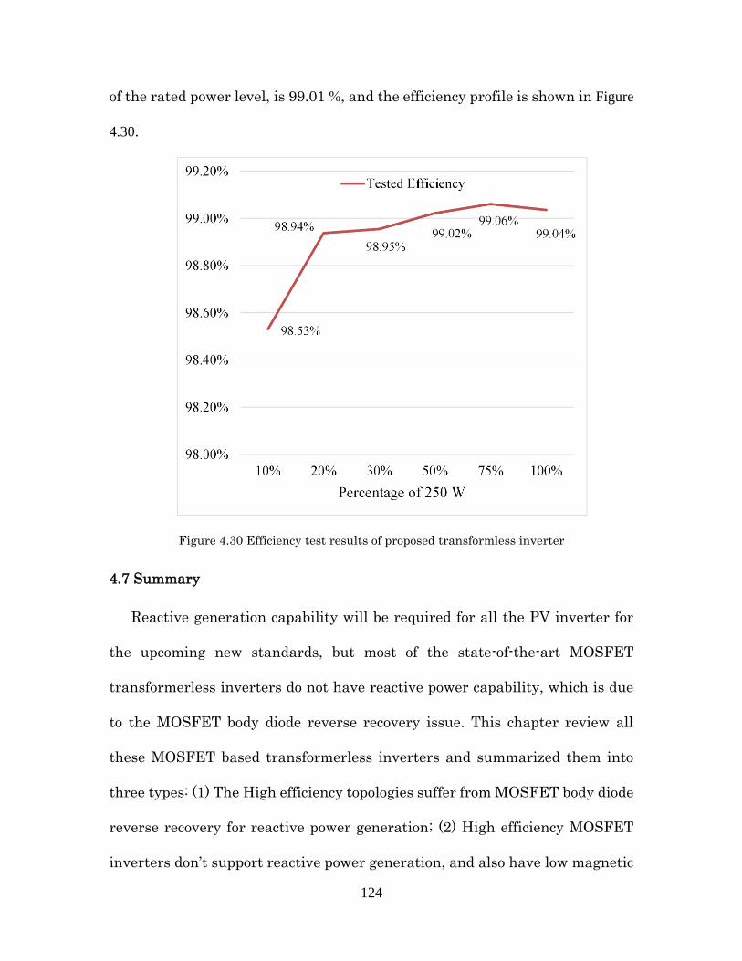
124
of the rated power level, is 99.01 %, and the efficiency profile is shown in Figure
4.30.
Figure 4.30 Efficiency test results of proposed transformless inverter
4.7 Summary
Reactive generation capability will be required for all the PV inverter for
the upcoming new standards, but most of the state-of-the-art MOSFET
transformerless inverters do not have reactive power capability, which is due
to the MOSFET body diode reverse recovery issue. This chapter review all
these MOSFET based transformerless inverters and summarized them into
three types: (1) The High efficiency topologies suffer from MOSFET body diode
reverse recovery for reactive power generation; (2) High efficiency MOSFET
inverters don’t support reactive power generation, and also have low magnetic

125
utilization; (3) MOSFET inverter support reactive power generation, but have
low efficiency and low magnetic utilization.
Based on the analysis of MOSFET inverter for reactive power generation,
the high efficiency MOSFET based transformerless inverter in the Chapter 3
is introduced and improved for reactive power generation. The proposed
inverter operating principle and PWM algorithm for reactive power generation
are described in detail. The ground loop voltage is derived with common mode
and differential mode circuit analysis using the proposed PWM method. The
circuit analysis results indicate that the ground loop voltage will not contain
high-frequency component by the symmetrical design of inductors. A 250-W
micro-inverter hardware prototype has been designed and fabricated. Steady
state and transient operating modes are tested to demonstrate the validity of
proposed PWM method, the reactive power capability of proposed inverter, and
the high-frequency component free of ground loop voltage. The power stage
peak efficiency achieves 99.06% at 30-kHz operating frequency.
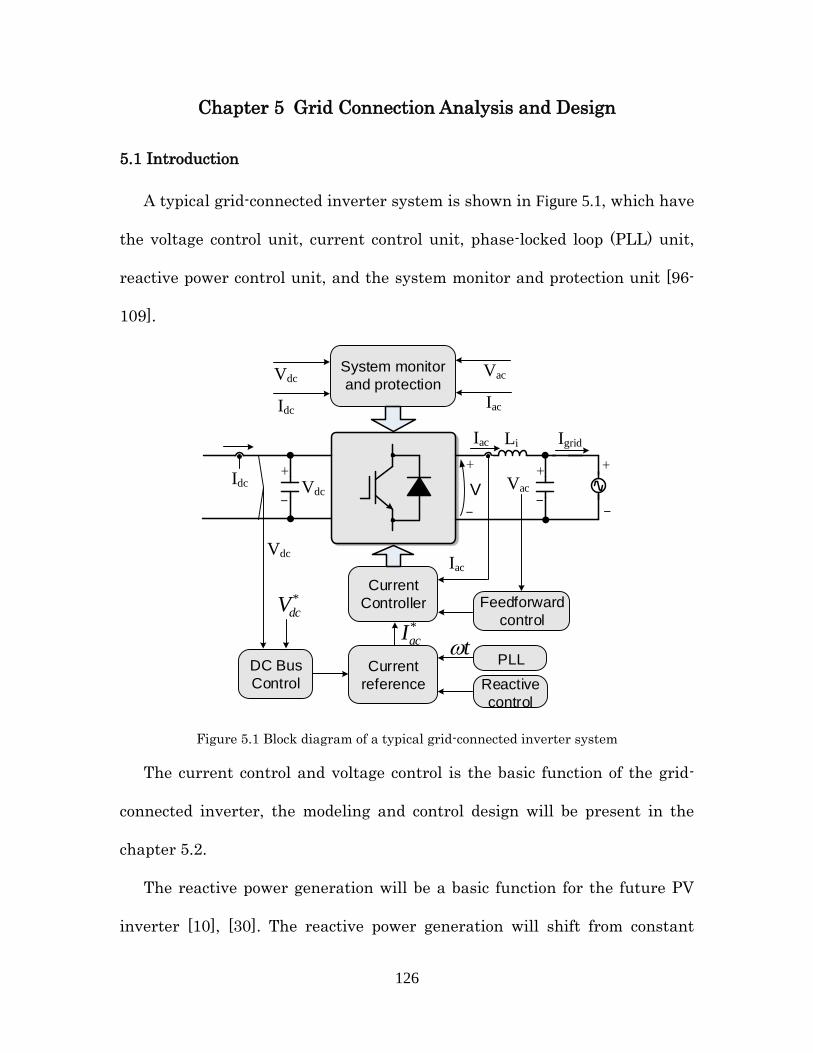
126
Chapter 5 Grid Connection Analysis and Design
5.1 Introduction
A typical grid-connected inverter system is shown in Figure 5.1, which have
the voltage control unit, current control unit, phase-locked loop (PLL) unit,
reactive power control unit, and the system monitor and protection unit [96-
109].
+
-
+
-
+
-V
Current
Controller
DC Bus
Control
+
-
VdcIac
Iac Li Igrid
VacIdc Vdc
Current
reference
Feedforward
control
PLL
*dcV
t*acI
Reactive
control
System monitor
and protection
Idc
VdcVac
Iac
Figure 5.1 Block diagram of a typical grid-connected inverter system
The current control and voltage control is the basic function of the grid-
connected inverter, the modeling and control design will be present in the
chapter 5.2.
The reactive power generation will be a basic function for the future PV
inverter [10], [30]. The reactive power generation will shift from constant
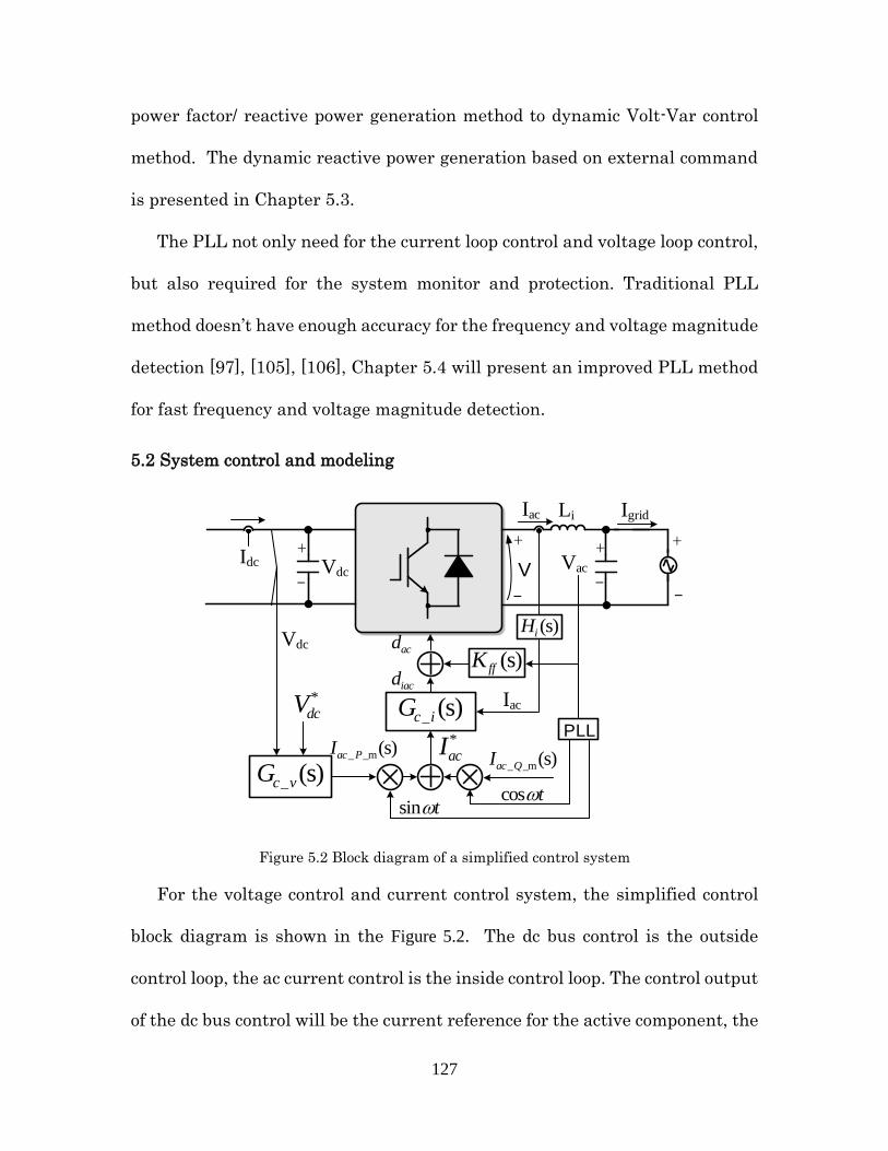
127
power factor/ reactive power generation method to dynamic Volt-Var control
method. The dynamic reactive power generation based on external command
is presented in Chapter 5.3.
The PLL not only need for the current loop control and voltage loop control,
but also required for the system monitor and protection. Traditional PLL
method doesn’t have enough accuracy for the frequency and voltage magnitude
detection [97], [105], [106], Chapter 5.4 will present an improved PLL method
for fast frequency and voltage magnitude detection.
5.2 System control and modeling
+
-
+
-
+
-V
+
-
Vdc
Iac
Iac Li Igrid
VacIdc Vdc
*dcV
*acI
_ (s)c vG
_ (s)c iG
_ _m(s)ac PI_ _m(s)ac QI
(s)ffK
PLL
costsint
iacd
acd(s)iH
Figure 5.2 Block diagram of a simplified control system
For the voltage control and current control system, the simplified control
block diagram is shown in the Figure 5.2. The dc bus control is the outside
control loop, the ac current control is the inside control loop. The control output
of the dc bus control will be the current reference for the active component, the
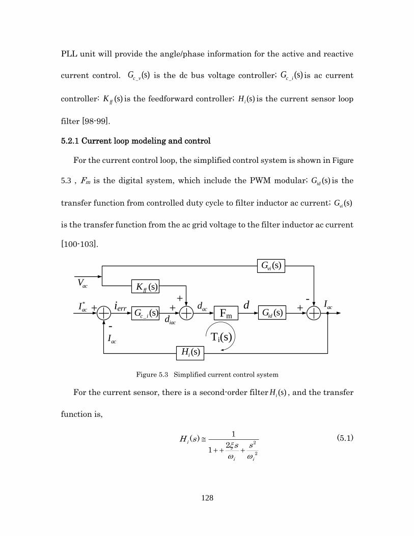
128
PLL unit will provide the angle/phase information for the active and reactive
current control. _ (s)c vG is the dc bus voltage controller; _ (s)c iG is ac current
controller: (s)ffK is the feedforward controller; (s)iH is the current sensor loop
filter [98-99].
5.2.1 Current loop modeling and control
For the current control loop, the simplified control system is shown in Figure
5.3 , Fm is the digital system, which include the PWM modular; (s)idG is the
transfer function from controlled duty cycle to filter inductor ac current; (s)viG
is the transfer function from the ac grid voltage to the filter inductor ac current
[100-103].
Fm
++ ++
-
ierr
-
Ti(s)
d*acI
acI
_ (s)c iGiacd
acd(s)idG
(s)iH
(s)viG
(s)ffKacV
acI
Figure 5.3 Simplified current control system
For the current sensor, there is a second-order filter (s)iH , and the transfer
function is,
2
2
1( )
21
i
i i
H ss s
(5.1)
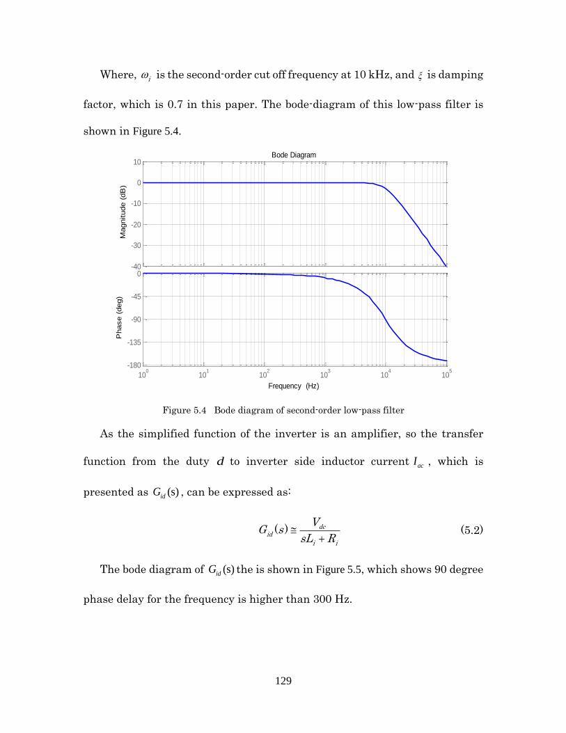
129
Where, i is the second-order cut off frequency at 10 kHz, and is damping
factor, which is 0.7 in this paper. The bode-diagram of this low-pass filter is
shown in Figure 5.4.
Figure 5.4 Bode diagram of second-order low-pass filter
As the simplified function of the inverter is an amplifier, so the transfer
function from the duty d to inverter side inductor current acI , which is
presented as (s)idG , can be expressed as:
( ) dcid
i i
VG s
sL R
(5.2)
The bode diagram of (s)idG the is shown in Figure 5.5, which shows 90 degree
phase delay for the frequency is higher than 300 Hz.
-40
-30
-20
-10
0
10
Magnitude (
dB
)
100
101
102
103
104
105
-180
-135
-90
-45
0
Phase (
deg)
Bode Diagram
Frequency (Hz)
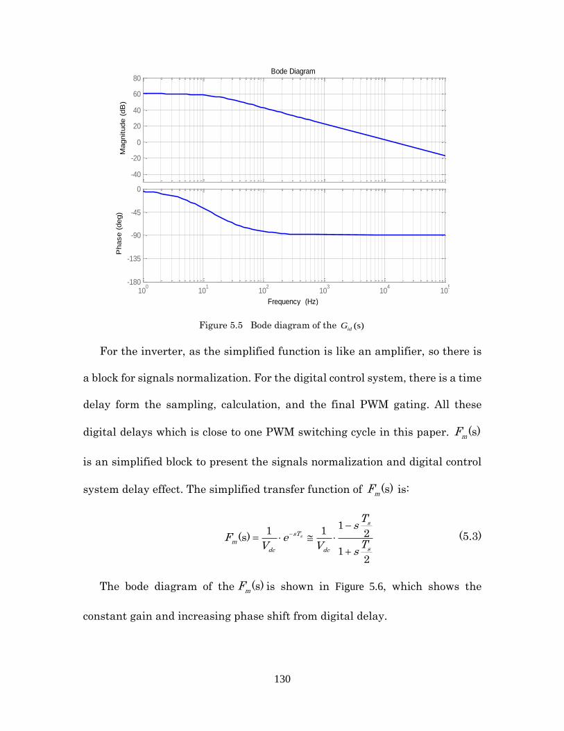
130
Figure 5.5 Bode diagram of the (s)idG
For the inverter, as the simplified function is like an amplifier, so there is
a block for signals normalization. For the digital control system, there is a time
delay form the sampling, calculation, and the final PWM gating. All these
digital delays which is close to one PWM switching cycle in this paper. (s)mF
is an simplified block to present the signals normalization and digital control
system delay effect. The simplified transfer function of (s)mF is:
1
1 1 2(s)
12
s
s
sT
msdc dc
Ts
F eTV V
s
(5.3)
The bode diagram of the (s)mF is shown in Figure 5.6, which shows the
constant gain and increasing phase shift from digital delay.
-40
-20
0
20
40
60
80
Magnitude (
dB
)
100
101
102
103
104
105
-180
-135
-90
-45
0
Phase (
deg)
Bode Diagram
Frequency (Hz)
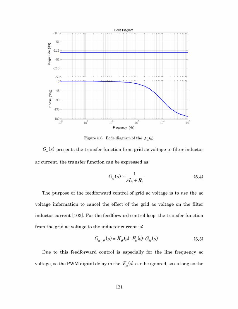
131
Figure 5.6 Bode diagram of the (s)mF
( )viG s presents the transfer function from grid ac voltage to filter inductor
ac current, the transfer function can be expressed as:
1
( )vi
i i
G ssL R
(5.4)
The purpose of the feedforward control of grid ac voltage is to use the ac
voltage information to cancel the effect of the grid ac voltage on the filter
inductor current [103]. For the feedforward control loop, the transfer function
from the grid ac voltage to the inductor current is:
_( ) (s) (s) ( )vi ff ff m idG s K F G s (5.5)
Due to this feedforward control is especially for the line frequency ac
voltage, so the PWM digital delay in the (s)mF can be ignored, so as long as the
-53
-52.5
-52
-51.5
-51
-50.5
Magnitude (
dB
)
100
101
102
103
104
105
-180
-135
-90
-45
0
Phase (
deg)
Bode Diagram
Frequency (Hz)
132
(s)ffK can achieve proper gain for the line frequency ac voltage, the grid ac
voltage on filter inductor ac current effect can be canceled under the condition
of :
_( ) ( )vi ff viG s G s (5.6)
With the feedforward control, the grid ac voltage on filter inductor ac
current effect can be canceled, so the current control loop can be simplified as
a single loop negative feedback control system, which is shown in Figure 5.7.
+
-
ierr
Ti(s)
d*acI
acI
_ (s)c iG
(s)iH
iacdmF (s)idG
acI
Figure 5.7 Simplified current control system with feedforward control
With the simplification of the feedforward control, the open loop transfer
function without current controller in Figure 5.7 (or the current control loop
plant _( )open diG s ) is:
_( )= (s) ( ) ( )open di m id iG s F G s H s (5.7)
The bode diagram of the current control loop plant _( )open diG s is shown in
the Figure 5.8.
For the current control, the proportional resonant (PR) controller is adopted
to minimize the 60 Hz steady-state error [104], the transfer function is
1 1_ 1 2 2
1
2( )
2r c
c i p
c o
k sG s k
s s
(5.8)
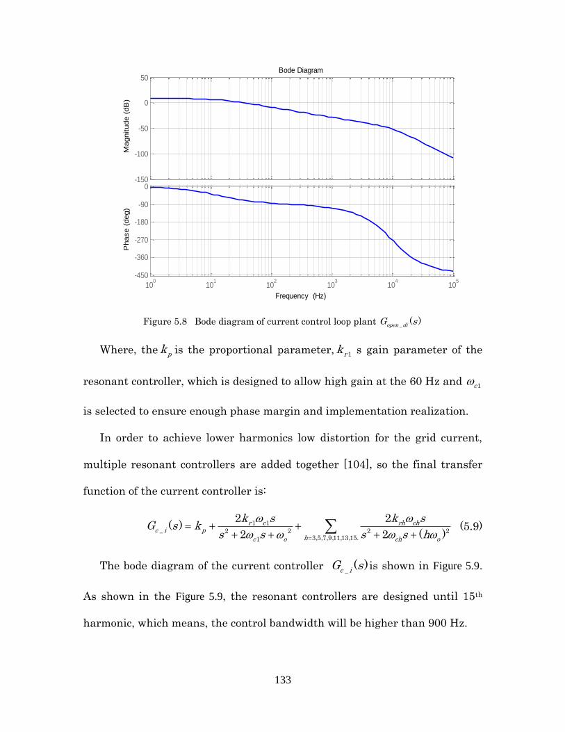
133
Figure 5.8 Bode diagram of current control loop plant _( )open diG s
Where, the pk is the proportional parameter, 1rk s gain parameter of the
resonant controller, which is designed to allow high gain at the 60 Hz and 1c
is selected to ensure enough phase margin and implementation realization.
In order to achieve lower harmonics low distortion for the grid current,
multiple resonant controllers are added together [104], so the final transfer
function of the current controller is:
1 1_ 2 2 2 2
3,5,7,9,11,13,15.1
2 2( )
2 2 ( )r c rh ch
c i phc o ch o
k s k sG s k
s s s s h
(5.9)
The bode diagram of the current controller _( )c iG s is shown in Figure 5.9.
As shown in the Figure 5.9, the resonant controllers are designed until 15th
harmonic, which means, the control bandwidth will be higher than 900 Hz.
-150
-100
-50
0
50
Magnitude (
dB
)
100
101
102
103
104
105
-450
-360
-270
-180
-90
0
Phase (
deg)
Bode Diagram
Frequency (Hz)
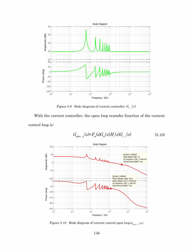
134
Figure 5.9 Bode diagram of current controller _( )c iG s
With the current controller, the open loop transfer function of the current
control loop is:
_ _( )= (s) ( ) ( ) ( )open ii m id i c iG s F G s H s G s (5.10)
Figure 5.10 Bode diagram of current control open loop_
( )open iiG s
20
30
40
50
60
Magnitude (
dB
)
100
101
102
103
104
105
-180
-135
-90
-45
0
45
90
Phase (
deg)
Bode Diagram
Frequency (Hz)
Bode Diagram
Frequency (Hz)
-100
-50
0
50
100
System: untitled1Gain Margin (dB): 12At frequency (Hz): 4.44e+03Closed loop stable? Yes
Magnitude (
dB
)
100
101
102
103
104
105
-450
-360
-270
-180
-90
0
System: untitled1Phase Margin (deg): 55.4Delay Margin (sec): 0.000132At frequency (Hz): 1.16e+03Closed loop stable? Yes
Phase (
deg)
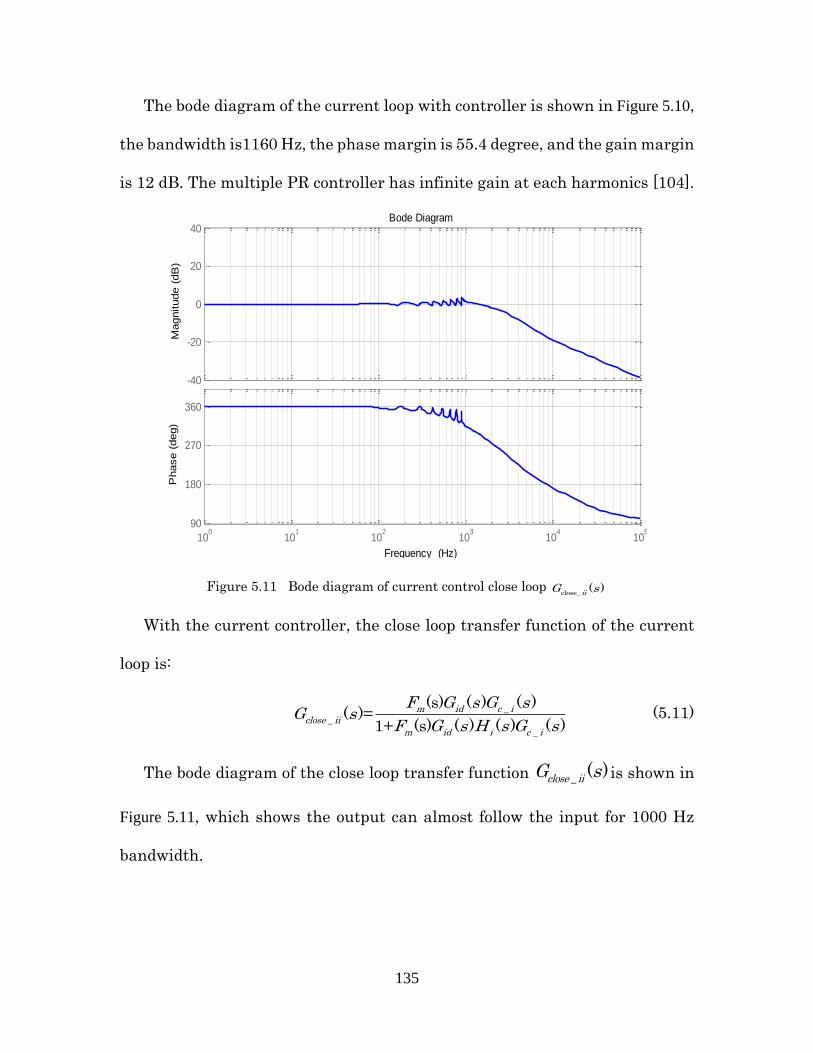
135
The bode diagram of the current loop with controller is shown in Figure 5.10,
the bandwidth is1160 Hz, the phase margin is 55.4 degree, and the gain margin
is 12 dB. The multiple PR controller has infinite gain at each harmonics [104].
Figure 5.11 Bode diagram of current control close loop close_
( )iiG s
With the current controller, the close loop transfer function of the current
loop is:
_
_
_
(s) ( ) ( )( )=
1+ (s) ( ) ( ) ( )
m id c i
close ii
m id i c i
F G s G sG s
F G s H s G s (5.11)
The bode diagram of the close loop transfer function _( )close iiG s is shown in
Figure 5.11, which shows the output can almost follow the input for 1000 Hz
bandwidth.
-40
-20
0
20
40
Magnitude (
dB
)
100
101
102
103
104
105
90
180
270
360
Phase (
deg)
Bode Diagram
Frequency (Hz)
136
5.2.2 DC voltage loop modeling and control
The current control loop has high bandwidthand is the inner loop, the
voltage control loop has very narrow bandwidth and is the outside loop. The
bandwidth of the current control loop is more than ten times higher than the
voltage controller loop, so each control loop can be designed independently. For
the voltage control loop, the 120Hz is a naturally result from the power
coupling, so it should be out of the dc voltage control loop bandwidth.
For the PV application, the dc PV power source can be modeled as a current
source IPV. The input and output energy relationship under steady state can
be expressed as:
PV dc ac acI V V I (5.12)
Under small disturbance theory, the relationship between the ac current
and dc voltage can be expressed as:
( )
( ) ( )dc dcPV dc dc dc dc ac ac ac
d V vI V v V C V I I
dt
(5.13)
The relationship between ac current disturbance and the dc voltage
disturbance is:
dcPV dc dc dc ac ac
d vI v V C V I
dt
(5.14)
So, the transfer function from ac current to dc voltage is:
_V(s)
ac dc
dc aci
PV dc dcac
v VG
I sV CI
(5.15)
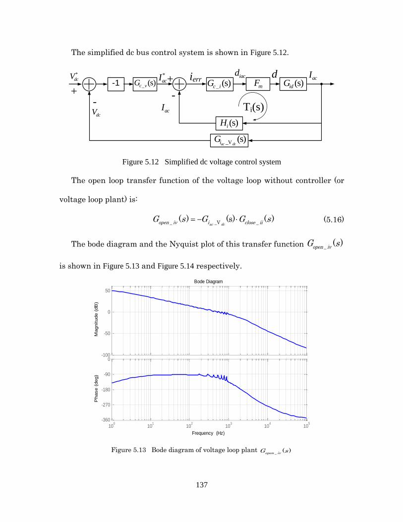
137
The simplified dc bus control system is shown in Figure 5.12.
+
-
ierr
Ti(s)
d*acI
acI
_ (s)c iG
(s)iH
iacd
mF (s)idGacI*
dcV_ (s)c vG
+-
dcV
_V (s)ac dciG
-1
Figure 5.12 Simplified dc voltage control system
The open loop transfer function of the voltage loop without controller (or
voltage loop plant) is:
_ _V _( ) (s) ( )
ac dcopen iv i close iiG s G G s (5.16)
The bode diagram and the Nyquist plot of this transfer function _( )open ivG s
is shown in Figure 5.13 and Figure 5.14 respectively.
Figure 5.13 Bode diagram of voltage loop plant _
( )open ivG s
Bode Diagram
Frequency (Hz)
-100
-50
0
50
Magnitude (
dB
)
100
101
102
103
104
105
-360
-270
-180
-90
0
Phase (
deg)
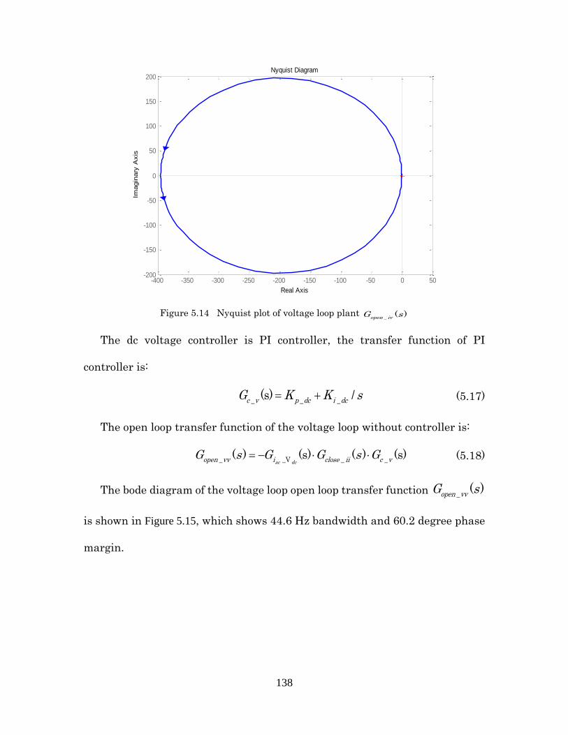
138
Figure 5.14 Nyquist plot of voltage loop plant _
( )open ivG s
The dc voltage controller is PI controller, the transfer function of PI
controller is:
_ _ _(s) /c v p dc i dcG K K s (5.17)
The open loop transfer function of the voltage loop without controller is:
_ _V _ _( ) (s) ( ) (s)
ac dcopen vv i close ii c vG s G G s G (5.18)
The bode diagram of the voltage loop open loop transfer function _( )open vvG s
is shown in Figure 5.15, which shows 44.6 Hz bandwidth and 60.2 degree phase
margin.
Nyquist Diagram
Real Axis
Imagin
ary
Axis
-400 -350 -300 -250 -200 -150 -100 -50 0 50-200
-150
-100
-50
0
50
100
150
200
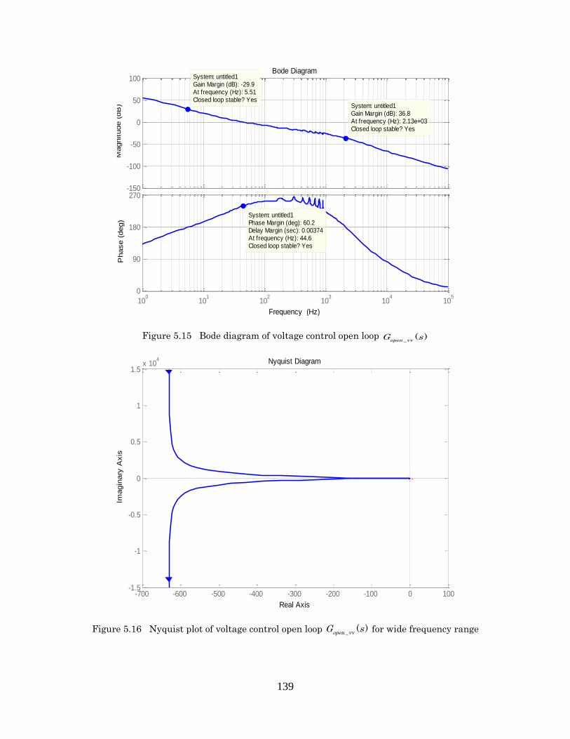
139
Figure 5.15 Bode diagram of voltage control open loop _
( )open vvG s
Figure 5.16 Nyquist plot of voltage control open loop _( )open vvG s for wide frequency range
Bode Diagram
Frequency (Hz)
100
101
102
103
104
105
0
90
180
270
System: untitled1Phase Margin (deg): 60.2Delay Margin (sec): 0.00374At frequency (Hz): 44.6Closed loop stable? Yes
Phase (
deg)
-150
-100
-50
0
50
100
System: untitled1Gain Margin (dB): 36.8At frequency (Hz): 2.13e+03Closed loop stable? Yes
System: untitled1Gain Margin (dB): -29.9At frequency (Hz): 5.51Closed loop stable? Yes
Magnitude (
dB
)
-700 -600 -500 -400 -300 -200 -100 0 100-1.5
-1
-0.5
0
0.5
1
1.5x 10
4 Nyquist Diagram
Real Axis
Imagin
ary
Axis
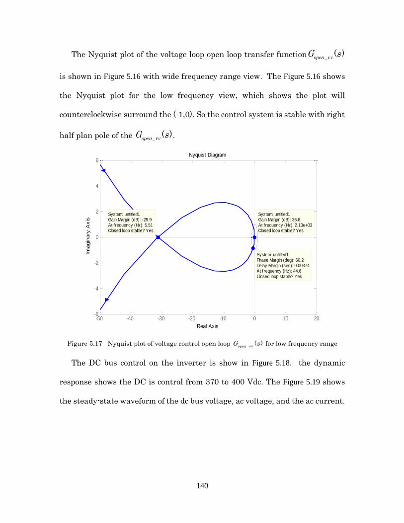
140
The Nyquist plot of the voltage loop open loop transfer function _( )open vvG s
is shown in Figure 5.16 with wide frequency range view. The Figure 5.16 shows
the Nyquist plot for the low frequency view, which shows the plot will
counterclockwise surround the (-1,0). So the control system is stable with right
half plan pole of the _( )open vvG s .
Figure 5.17 Nyquist plot of voltage control open loop _( )open vvG s for low frequency range
The DC bus control on the inverter is show in Figure 5.18. the dynamic
response shows the DC is control from 370 to 400 Vdc. The Figure 5.19 shows
the steady-state waveform of the dc bus voltage, ac voltage, and the ac current.
Nyquist Diagram
Real Axis
Imagin
ary
Axis
-50 -40 -30 -20 -10 0 10 20-6
-4
-2
0
2
4
6
System: untitled1Gain Margin (dB): 36.8At frequency (Hz): 2.13e+03Closed loop stable? Yes
System: untitled1Phase Margin (deg): 60.2Delay Margin (sec): 0.00374At frequency (Hz): 44.6Closed loop stable? Yes
System: untitled1Gain Margin (dB): -29.9At frequency (Hz): 5.51Closed loop stable? Yes
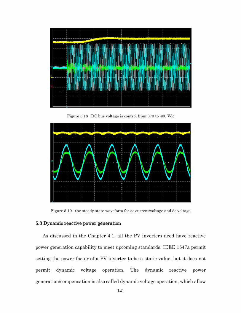
141
Figure 5.18 DC bus voltage is control from 370 to 400 Vdc
Figure 5.19 the steady state waveform for ac current/voltage and dc voltage
5.3 Dynamic reactive power generation
As discussed in the Chapter 4.1, all the PV inverters need have reactive
power generation capability to meet upcoming standards. IEEE 1547a permit
setting the power factor of a PV inverter to be a static value, but it does not
permit dynamic voltage operation. The dynamic reactive power
generation/compensation is also called dynamic voltage operation, which allow

142
distribution power system to counteract voltage deviation from the nominal
voltage level by consuming or producing reactive power. The purpose of
reactive power generation/ compensation is used to help power grid to maintain
voltage levels with the system normal ranges. The difference between the
constant power factor running and the dynamic reactive power generation is
that the inverter can actively regulate the voltage at the point of common
coupling (PCC) [107-109].
Traditional reactive power generation methods usually are based on an
established “curve” which define the voltage versus the percentage of reactive
power. The percentage of reactive power can be calculated as:
(1) Percentage of available reactive power for the measured percentage of
the reference voltage. “Available Vars” implies the consumption or
production of reactive power that does not affect the real power output.
(2) Percentage of maximum reactive power. In this case, consumption or
production of reactive power may affect the real power output.
The curve of the Voltage-Var control with dead-band method is shown in
Figure 5.20, which use a dead-band between V2 and V3 around the nominal
voltage[107-108].
The curve of the Voltage-Var control with hysteresis method is shown in
Figure 5.21, which use a hysteresis to dampen the unnecessary swings for the
boundary condition.
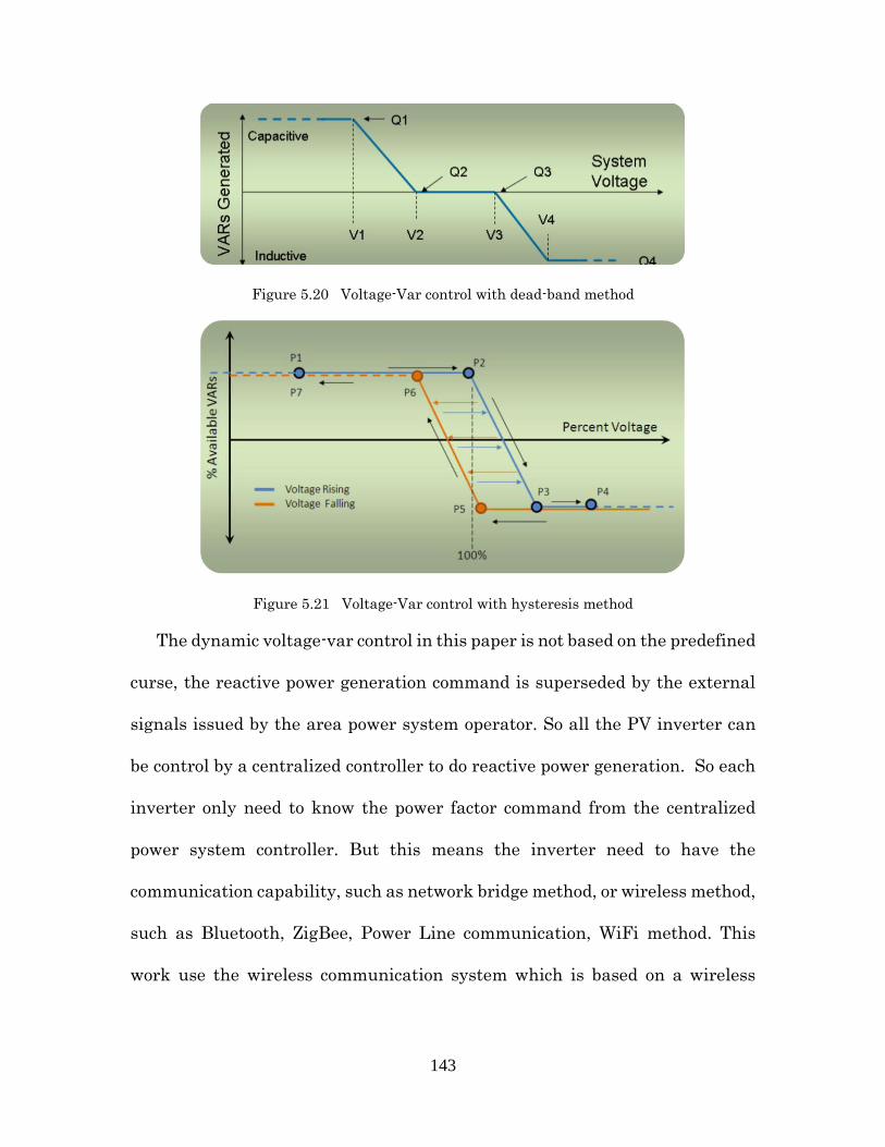
143
Figure 5.20 Voltage-Var control with dead-band method
Figure 5.21 Voltage-Var control with hysteresis method
The dynamic voltage-var control in this paper is not based on the predefined
curse, the reactive power generation command is superseded by the external
signals issued by the area power system operator. So all the PV inverter can
be control by a centralized controller to do reactive power generation. So each
inverter only need to know the power factor command from the centralized
power system controller. But this means the inverter need to have the
communication capability, such as network bridge method, or wireless method,
such as Bluetooth, ZigBee, Power Line communication, WiFi method. This
work use the wireless communication system which is based on a wireless
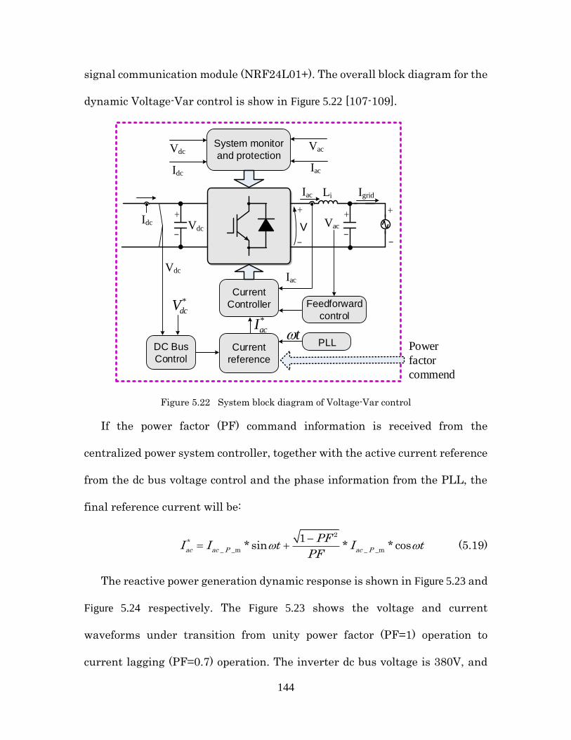
144
signal communication module (NRF24L01+). The overall block diagram for the
dynamic Voltage-Var control is show in Figure 5.22 [107-109].
+
-
+
-
+
-V
Current
Controller
DC Bus
Control
+
-
VdcIac
Iac Li Igrid
VacIdc Vdc
Current
reference
Feedforward
control
PLL
*dcV
t*acI
System monitor
and protection
Idc
VdcVac
Iac
Power
factor
commend
Figure 5.22 System block diagram of Voltage-Var control
If the power factor (PF) command information is received from the
centralized power system controller, together with the active current reference
from the dc bus voltage control and the phase information from the PLL, the
final reference current will be:
2
*
_ _m _ _m
1* sin * * cosac ac P ac P
PFI I t I t
PF
(5.19)
The reactive power generation dynamic response is shown in Figure 5.23 and
Figure 5.24 respectively. The Figure 5.23 shows the voltage and current
waveforms under transition from unity power factor (PF=1) operation to
current lagging (PF=0.7) operation. The inverter dc bus voltage is 380V, and
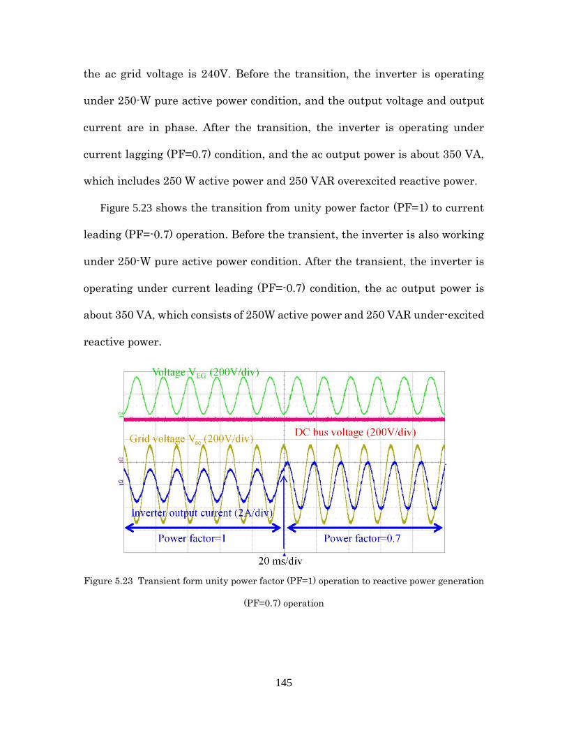
145
the ac grid voltage is 240V. Before the transition, the inverter is operating
under 250-W pure active power condition, and the output voltage and output
current are in phase. After the transition, the inverter is operating under
current lagging (PF=0.7) condition, and the ac output power is about 350 VA,
which includes 250 W active power and 250 VAR overexcited reactive power.
Figure 5.23 shows the transition from unity power factor (PF=1) to current
leading (PF=-0.7) operation. Before the transient, the inverter is also working
under 250-W pure active power condition. After the transient, the inverter is
operating under current leading (PF=-0.7) condition, the ac output power is
about 350 VA, which consists of 250W active power and 250 VAR under-excited
reactive power.
Figure 5.23 Transient form unity power factor (PF=1) operation to reactive power generation
(PF=0.7) operation
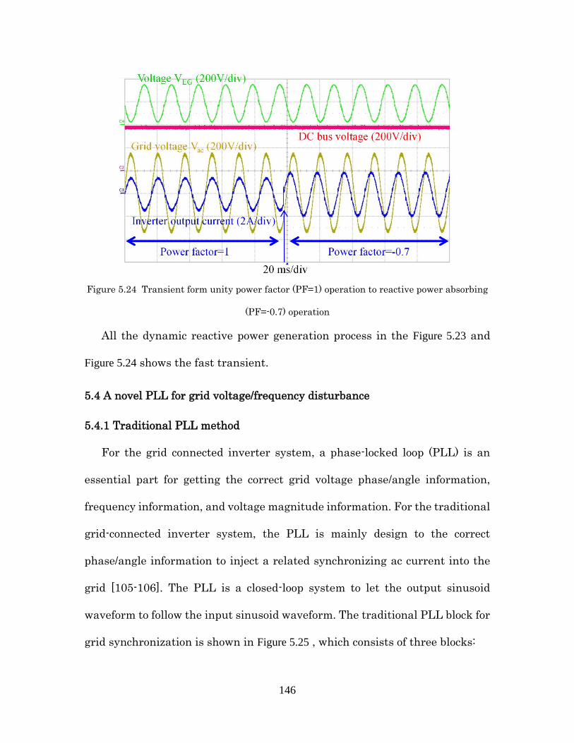
146
Figure 5.24 Transient form unity power factor (PF=1) operation to reactive power absorbing
(PF=-0.7) operation
All the dynamic reactive power generation process in the Figure 5.23 and
Figure 5.24 shows the fast transient.
5.4 A novel PLL for grid voltage/frequency disturbance
5.4.1 Traditional PLL method
For the grid connected inverter system, a phase-locked loop (PLL) is an
essential part for getting the correct grid voltage phase/angle information,
frequency information, and voltage magnitude information. For the traditional
grid-connected inverter system, the PLL is mainly design to the correct
phase/angle information to inject a related synchronizing ac current into the
grid [105-106]. The PLL is a closed-loop system to let the output sinusoid
waveform to follow the input sinusoid waveform. The traditional PLL block for
grid synchronization is shown in Figure 5.25 , which consists of three blocks:
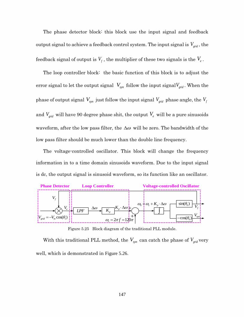
147
The phase detector block: this block use the input signal and feedback
output signal to achieve a feedback control system. The input signal is gridV , the
feedback signal of output is fV , the multiplier of these two signals is the eV .
The loop controller block: the basic function of this block is to adjust the
error signal to let the output signal synV follow the input signal gridV . When the
phase of output signal synV just follow the input signal gridV phase angle, the fV
and gridV will have 90 degree phase shit, the output eV will be a pure sinusoids
waveform, after the low pass filter, the will be zero. The bandwidth of the
low pass filter should be much lower than the double line frequency.
The voltage-controlled oscillator. This block will change the frequency
information in to a time domain sinusoids waveform. Due to the input signal
is dc, the output signal is sinusoid waveform, so its function like an oscillator.
1cos( )grid mV V
fV
eV +
2 120 c f+
pK0 c pK
LPF pK
0cos( )
0sin( )fV
synV
Phase Detector Loop Controller Voltage-controlled Oscillator
Figure 5.25 Block diagram of the traditional PLL module.
With this traditional PLL method, the synV can catch the phase of gridV very
well, which is demonstrated in Figure 5.26.
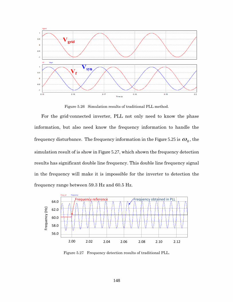
148
Figure 5.26 Simulation results of traditional PLL method.
For the grid-connected inverter, PLL not only need to know the phase
information, but also need know the frequency information to handle the
frequency disturbance. The frequency information in the Figure 5.25 is 0 , the
simulation result of is show in Figure 5.27, which shown the frequency detection
results has significant double line frequency. This double line frequency signal
in the frequency will make it is impossible for the inverter to detection the
frequency range between 59.3 Hz and 60.5 Hz.
Figure 5.27 Frequency detection results of traditional PLL.
54
56
58
60
62
64
Freq_ref Frequency
2 2.02 2.04 2.06 2.08 2.1 2.12
Time (s)
0
-0.5
-1
0.5
1
V1
64.0
62.0
60.0
58.0
56.0
Freq
uen
cy (
Hz)
Frequency reference Frequency obtained in PLL
2.00 2.062.042.02 2.102.08 2.12
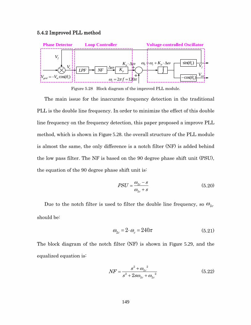
149
5.4.2 Improved PLL method
1cos( )grid mV V
fV
eV +
2 120 c f+
pK 0 c pK
LPF pK
0cos( )
0sin( )fV
synV
Phase Detector Loop Controller Voltage-controlled Oscillator
NF
Figure 5.28 Block diagram of the improved PLL module.
The main issue for the inaccurate frequency detection in the traditional
PLL is the double line frequency. In order to minimize the effect of this double
line frequency on the frequency detection, this paper proposed a improve PLL
method, which is shown in Figure 5.28. the overall structure of the PLL module
is almost the same, the only difference is a notch filter (NF) is added behind
the low pass filter. The NF is based on the 90 degree phase shift unit (PSU),
the equation of the 90 degree phase shift unit is:
2
2
c
c
sPSU
s
(5.20)
Due to the notch filter is used to filter the double line frequency, so 2c
should be:
22 240c c (5.21)
The block diagram of the notch filter (NF) is shown in Figure 5.29, and the
equalized equation is:
2 2
2
2 2
2 22
c
c c
sNF
s s
(5.22)
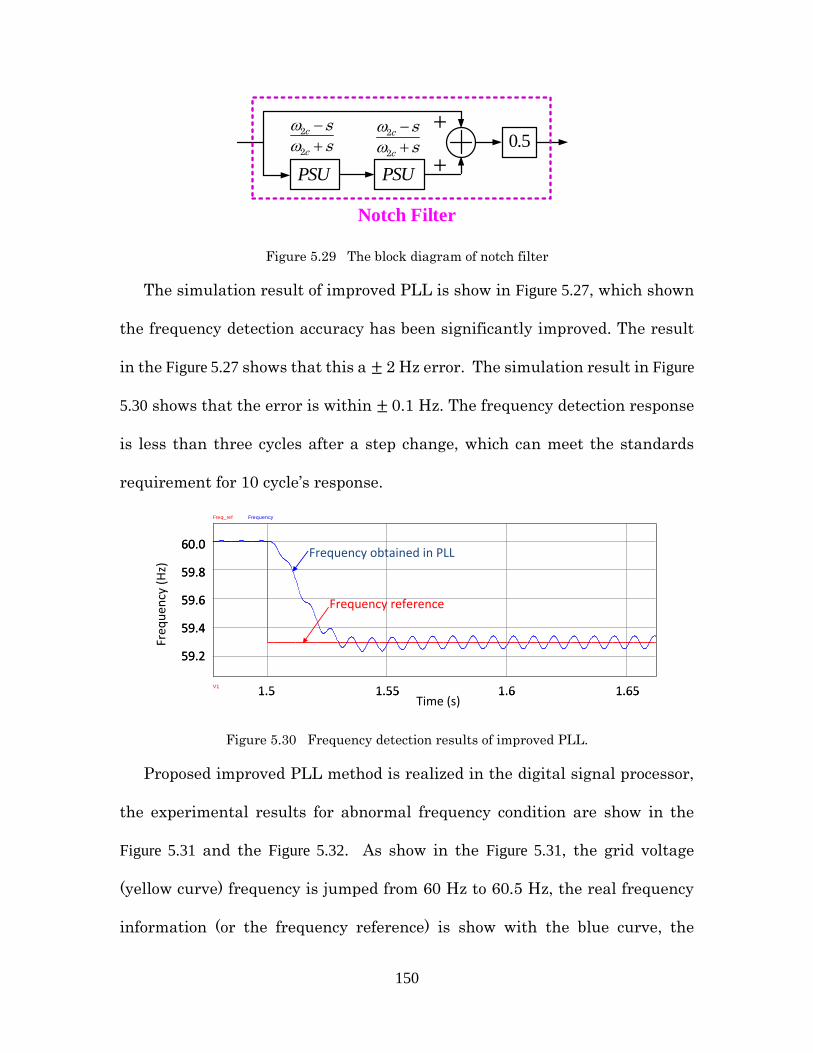
150
PSU PSU
0.5+
+
Notch Filter
2
2
c
c
s
s
2
2
c
c
s
s
Figure 5.29 The block diagram of notch filter
The simulation result of improved PLL is show in Figure 5.27, which shown
the frequency detection accuracy has been significantly improved. The result
in the Figure 5.27 shows that this a ± 2 Hz error. The simulation result in Figure
5.30 shows that the error is within ± 0.1 Hz. The frequency detection response
is less than three cycles after a step change, which can meet the standards
requirement for 10 cycle’s response.
Figure 5.30 Frequency detection results of improved PLL.
Proposed improved PLL method is realized in the digital signal processor,
the experimental results for abnormal frequency condition are show in the
Figure 5.31 and the Figure 5.32. As show in the Figure 5.31, the grid voltage
(yellow curve) frequency is jumped from 60 Hz to 60.5 Hz, the real frequency
information (or the frequency reference) is show with the blue curve, the
59.2
59.4
59.6
59.8
60
Freq_ref Frequency
1.5 1.55 1.6 1.65
Time (s)
0
-0.5
-1
0.5
1
V1
60.0
59.8
59.6
59.4
59.2
1.61.551.5 1.65
59.2
59.4
59.6
59.8
60
Freq_ref Frequency
1.5 1.55 1.6 1.65
Time (s)
0
-0.5
-1
0.5
1
V1
60.0
59.8
59.6
59.4
59.2
1.61.551.5 1.65Time (s)
Freq
uen
cy (
Hz)
Frequency obtained in PLL
Frequency reference
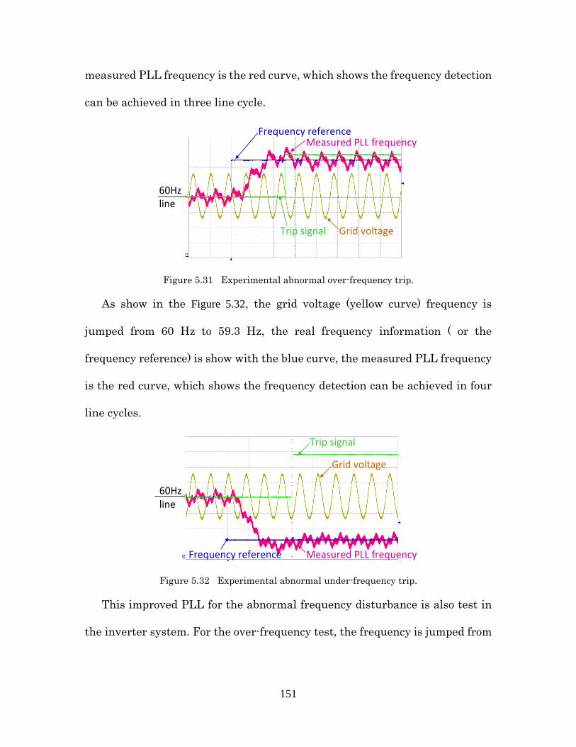
151
measured PLL frequency is the red curve, which shows the frequency detection
can be achieved in three line cycle.
Figure 5.31 Experimental abnormal over-frequency trip.
As show in the Figure 5.32, the grid voltage (yellow curve) frequency is
jumped from 60 Hz to 59.3 Hz, the real frequency information ( or the
frequency reference) is show with the blue curve, the measured PLL frequency
is the red curve, which shows the frequency detection can be achieved in four
line cycles.
Figure 5.32 Experimental abnormal under-frequency trip.
This improved PLL for the abnormal frequency disturbance is also test in
the inverter system. For the over-frequency test, the frequency is jumped from
Measured PLL frequencyFrequency reference
Grid voltage Trip signal
60Hz line
Frequency reference Measured PLL frequency
Grid voltage
Trip signal
60Hz line
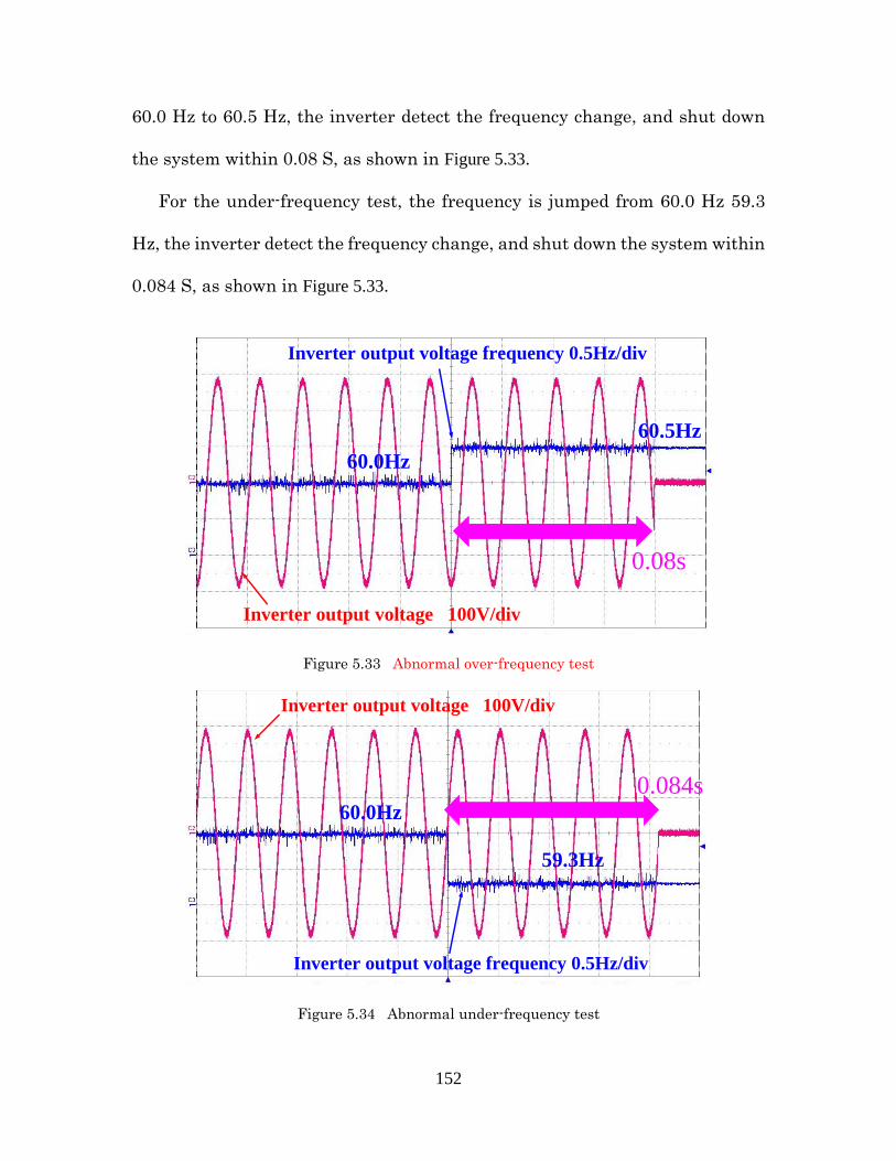
152
60.0 Hz to 60.5 Hz, the inverter detect the frequency change, and shut down
the system within 0.08 S, as shown in Figure 5.33.
For the under-frequency test, the frequency is jumped from 60.0 Hz 59.3
Hz, the inverter detect the frequency change, and shut down the system within
0.084 S, as shown in Figure 5.33.
Figure 5.33 Abnormal over-frequency test
Figure 5.34 Abnormal under-frequency test
Inverter output voltage 100V/div
Inverter output voltage frequency 0.5Hz/div
60.5Hz
60.0Hz
0.08s
Inverter output voltage 100V/div
Inverter output voltage frequency 0.5Hz/div
59.3Hz
60.0Hz
0.084s
153
Table 5-1 Summary of abnormal frequency test results
Frequency range
(Hz)
Disconnection Time (s)
IEEE 1547 Inverter Test Result
f> 60.5
f< 59.3
0.16
0.084
5.4.3 Voltage magnitude detection method
The grid voltage magnitude is an important information for power
calculation, voltage protection. For the grid-connected PV inverter, another
importance of the voltage magnitude detection is for the voltage disturbance
reaction. Under different under voltage or over voltage condition, the inverter
need to stay with normal connection or disconnection within specified time
[105-109].
The voltage magnitude detection method in this paper is also based on the
90 degree phase shit unit, this phase shift unit is design for the line frequency,
so the transfer function is:
1c
c
sPSU
s
(5.23)
The voltage magnitude detection is shown in Figure 5.35.
PSUacV *
acV 22 *ac acV V
magV
ac
grid
mag
VV
V
Magnitude
Unit sinusoid
Figure 5.35 Voltage magnitude detection method
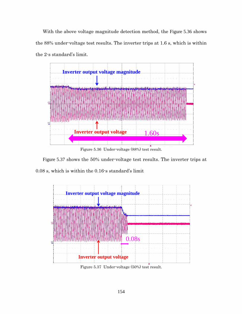
154
With the above voltage magnitude detection method, the Figure 5.36 shows
the 88% under-voltage test results. The inverter trips at 1.6 s, which is within
the 2-s standard’s limit.
Figure 5.36 Under-voltage (88%) test result.
Figure 5.37 shows the 50% under-voltage test results. The inverter trips at
0.08 s, which is within the 0.16-s standard’s limit
Figure 5.37 Under-voltage (50%) test result.
Inverter output voltage
Inverter output voltage magnitude
1.60s
Inverter output voltage
Inverter output voltage magnitude
0.08s
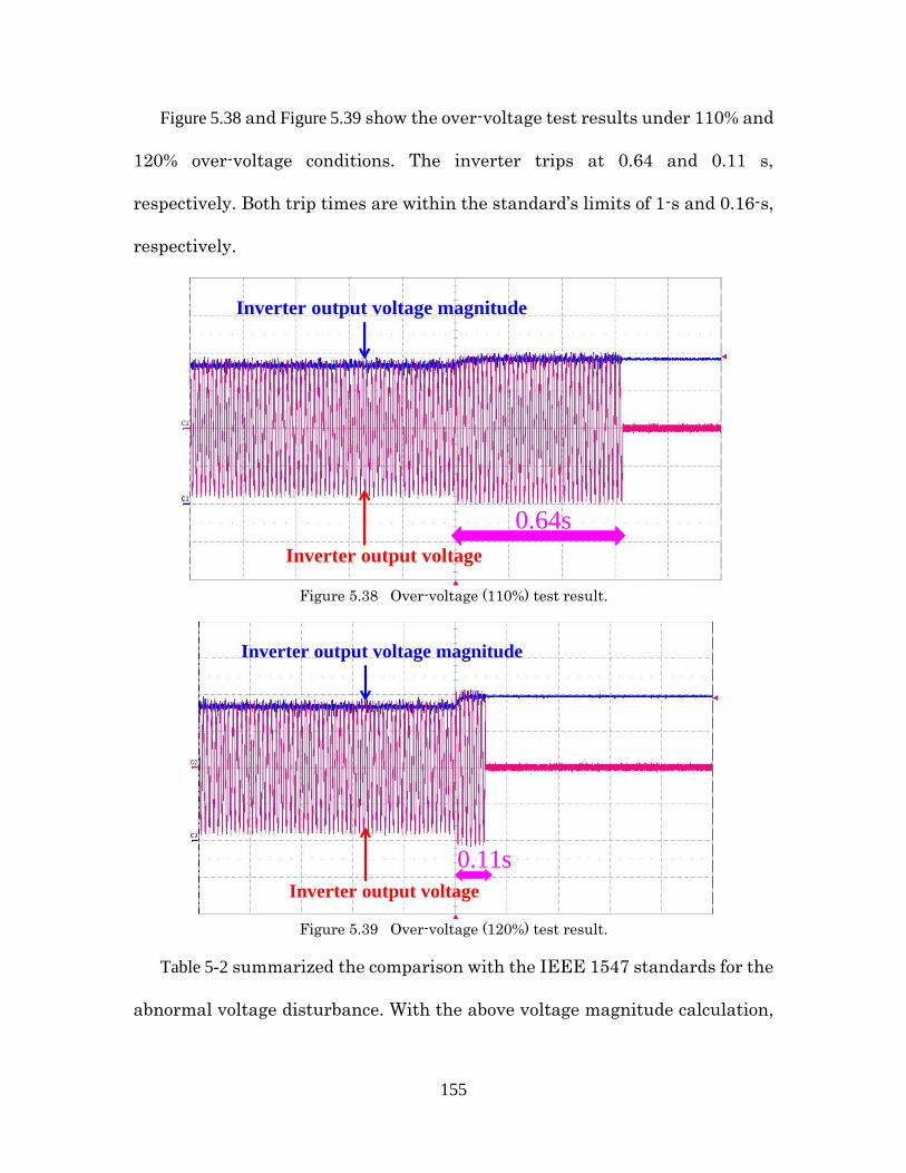
155
Figure 5.38 and Figure 5.39 show the over-voltage test results under 110% and
120% over-voltage conditions. The inverter trips at 0.64 and 0.11 s,
respectively. Both trip times are within the standard’s limits of 1-s and 0.16-s,
respectively.
Figure 5.38 Over-voltage (110%) test result.
Figure 5.39 Over-voltage (120%) test result.
Table 5-2 summarized the comparison with the IEEE 1547 standards for the
abnormal voltage disturbance. With the above voltage magnitude calculation,
Inverter output voltage
Inverter output voltage magnitude
0.64s
Inverter output voltage
Inverter output voltage magnitude
0.11s
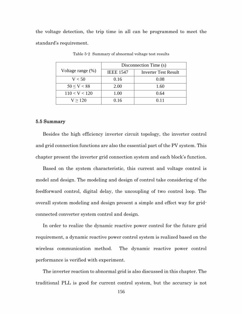
156
the voltage detection, the trip time in all can be programmed to meet the
standard’s requirement.
Table 5-2 Summary of abnormal voltage test results
Voltage range (%)
Disconnection Time (s)
IEEE 1547 Inverter Test Result
V < 50 0.16 0.08
50 ≤ V < 88 2.00 1.60
110 < V < 120 1.00 0.64
V ≥ 120 0.16 0.11
5.5 Summary
Besides the high efficiency inverter circuit topology, the inverter control
and grid connection functions are also the essential part of the PV system. This
chapter present the inverter grid connection system and each block’s function.
Based on the system characteristic, this current and voltage control is
model and design. The modeling and design of control take considering of the
feedforward control, digital delay, the uncoupling of two control loop. The
overall system modeling and design present a simple and effect way for grid-
connected converter system control and design.
In order to realize the dynamic reactive power control for the future grid
requirement, a dynamic reactive power control system is realized based on the
wireless communication method. The dynamic reactive power control
performance is verified with experiment.
The inverter reaction to abnormal grid is also discussed in this chapter. The
traditional PLL is good for current control system, but the accuracy is not

157
enough for the grid frequency disturbance detection and protection. This
chapter proposed an improved PLL, which can improve the accuracy
significantly to meet the standard requirement for the frequency disturbance.
A similar method is also adopted into the voltage magnitude detection method.
Experimental results demonstrate the validity of the proposed method for grid
disturbance detection and protection.

158
Chapter 6 Conclusions and Future Work
6.1 Conclusions
Power electronic converter is the heart of every PV plant, which is an
environmentally power generation system that uses the PV cells to convert
sunlight into electrical power. High efficiency is preferred for maxim solar
energy extraction, high reliable/low cost/low volume inverter design, and fast
custom investment return. State-of-the-art transformerless inverter can
reached around 97% efficiency. Some special transformerless inverter topology
can achieve more than 98% efficiency.
This dissertation viewed the state-of-the-art transformerless inverter high
efficiency topologies and summarized a new inverter technology. With this
new inverter technology, a family of high efficiency transformerless inverters
are proposed. The proposed inverters not only demonstrate the summarized
new inverter technology, but also offer a high efficiency and patent free
solutions.
Most of the innovative transformerless inverter topologies MOSFET to
boost efficiency. However, these MOSFET based inverter topologies suffer from
one or more of these drawbacks: MOSFET failure risk from body diode reverse
recovery, increased conduction losses due to more devices, or low magnetics
utilization. With a brief review of these MOSFET based transformeless
inverters, a novel MOSFET based phase-leg method is proposed. With this
proposed MOSFET phase-leg, a high efficiency MOSFET based
159
transformerless inverter is proposed. The experimental results of this
MOSFET based inverter not only demonstrate the validity of the proposed
MOSFET phase-leg method for high efficiency, high magnetic utilization, and
low risk from MOSFET body diode, but also provide a new way to build other
high efficiency transformerless inverters.
Due to the reactive power generation will be required for all the PV
inverters, and most of the state-of-the-art high efficiency MOSFET based
transformerless inverter don’t have reactive power generation capability. This
work improve the proposed high efficiency MOSFET transformerless inverter,
and a novel PWM is proposed for the reactive power generation. Experimental
result demonstrate the validity of this improve transformerless inverter and
the reactive power generation capability.
Besides the high efficiency inverter circuit, the grid connection function is
also the essential part of the PV system. The current control and voltage
control loop is analyzed, model, and designed. The dynamic reactive power
generation is also realized in the control system. The new PLL method for the
grid frequency/voltage disturbance is also realized and demonstrate the
validity of the detection and protection capability for the voltage/frequency
disturbance.
The work in this research has resulted in the following contributions:
1. Based the review of the state-of-the-art transformerless inverter
topologies, a new inverter technology is summarized. The new inverter

160
technology is named as Neutral Point Virtually Clamped (V-NPC)
inverter topology.
2. With the principle of V-NPC inverter technology, a family high efficiency
transformerless inverters are proposed. A 250 W hardware prototype is
designed and tested to demonstrate the low common mode voltage and
98.96% peak efficiency. The ground loop voltage analysis method is also
presented, which is based on the CM and DM model.
3. A novel MOSFET based phase-leg is proposed for high efficiency
inverters. Based on the this proposed MOSFET phase-leg, a 99.06%
peak efficieny MOSFET based transformerless inverter is proposed,
which also has high magnetic utilization and avoid the MOSFET body
diode reverse recovery.
4. A novel PWM method is proposed for the reactive power generation of
proposed MOSFET inverter.
5. Current loop and voltage loop model have been both derived and
designed. The dynamic reactive power generation is also realized in the
control system. The new PLL method for the grid frequency/voltage
disturbance is also realized and demonstrate the validity of the detection
and protection capability for the voltage/frequency disturbance.
6.2 Future work
The research work in this dissertation demonstrates promising
performance in high efficiency transformerless inverter circuit, using

161
MOSFET to replace the IGBT in the high efficiency transformerless inverter,
realized reactive power generation with MOSFET based transformerless
inverter, and high performance for grid connection function. However, there
are other areas where further investigations will be required to increase the
overall performance of the system efficiency and function capability. The
following topics are recommended for future work.
Device package
In the proposed high efficiency MOSFET based transformerless inverter
system, there are a lot discrete power devices. For the power circuit, the high
efficiency means high frequency and high power density. So with proper device
package, such as all the discrete power devices are packaged in one module,
the overall size can be minimized, the parasitic can be also minimized for
higher efficiency.
New inverter circuit with V-NPC method
With the review of state-of-the-art transformerless inverters, the V-NPC
method is summarized, and a family of high efficiency transformerless inverter
is proposed. New inverter circuit can be derived through this V-NPC method,
which will be an interesting topic for future research.
New power electronics circuit with proposed MOSFET phase-leg
With the review of state-of-the-art MSOFET based transformerless
inverters, the MOSFET based phase-leg method is summarized, and a high
efficiency transformerless MOSFET inverter is proposed and verified. This

162
MOSFET phase-leg method not only can be applied in to transformreless
inveter topology, but also can be applied to most of the phase-leg that want
adopted high voltage MOSFET. New power electronics circuit can be derived
through this proposed MOSFET based phase-leg, which will be an interesting
topic for future research.
Effect of reactive power generation on system cost and efficiency
The reactive power generation is realized on the proposed high efficiency
MOSFET based transformerless inverter. But the effects of the reactive power
generation on the cost and efficiency have never been discussed, which will be
a very practical research topic.
Standard compliance
New standard also requires the low voltage ride through, which is not done
in this work. Besides, more work need to be done for the inverter to pass the
UL1741.
List of publications
Different parts of this work have already been published or are being
published in international journals or conference proceedings. These
publications are listed below.
[1] B. F. Chen, B. Gu, and J. S. Lai, " "A Novel Pulse Width Modulation
Method for Reactive Power Generation on a CoolMOS and SiC Diode
163
based Transformerless Inverter", Accepted by IEEE Trans. Ind.
Electron. ,2016.
[2] B. F. Chen, B. Gu, L. H. Zhang, and J. S. Lai, " A Novel Pulse Width
Modulation Method for Reactive Power Generation on a CoolMOS and
SiC Diode based Transformerless Inverter", Accepted by IEEE Trans.
Ind. Electron. ,2015.
[3] L. H. Zhang, R. Born, B. Gu, B. F. Chen, C. Zheng, X. N. Zhao, and J.
S. Lai, "A Sensorless Implementation of the Parabolic Current Control
for Single-Phase Stand-Alone Inverters", Accepted by IEEE Trans.
Power Electron, 2015.
[4] B. F. Chen, C. Zheng, B. Gu, L. H. Zhang, and J. S. Lai , “A MOSFET
Transformerless Inverter with Reactive Power Capability for Micro-
inverter Applications,” in the Proc. of IEEE 30th Applied Power
Electronics Conference and Exposition, 2015.
[5] B. F. Chen and J. S. Lai , “A family of single-phase transformerless
inverters with asymmetric phase-legs,” in the Proc. of IEEE 30th Applied
Power Electronics Conference and Exposition, 2015.
[6] C. Zheng, B. F. Chen, L. H. Zhang, R. Chen, and J. S. Lai, “Design
considerations of LLC resonant converter for contactless laptop
charger,” in the Proc. of IEEE 30th Applied Power Electronics
Conference and Exposition, 2015.
[7] L. H. Zhang, J. Dominic, B. Gu, B. F. Chen, C. Zheng, and J. S Lai,
“Implementation of parabolic current control for dual-carrier PWM,” in
the Proc. of IEEE 30th Applied Power Electronics Conference and
Exposition, 2015.
[8] C.Y. Lin, Y.C. Liu, J.S. Lai, and B. F. Chen, “High-Voltage GaN HEMT
Evaluation in Micro-Inverter Applications,” in the Proc. of IEEE 30th
Applied Power Electronics Conference and Exposition, 2015.
164
[9] B. F. Chen, B. Gu, and J. S. Lai, “A High Efficiency MOSFET
Transformerless Inverter for Non-isolated Micro-inverter Applications,”
IEEE Trans. Power Electron, 10.1109/TPEL.2014.2339320, 2014.
[10] L. H. Zhang, B. Gu, J. Dominic, B. F. Chen, C. Zheng, and J. S. Lai, “A
Dead-time Compensation Method for Parabolic Current Control with
Improved Current Tracking and Enhanced Stability Range,” IEEE
Trans. Power Electron, 10.1109/TPEL.2014.2339302, 2014.
[11] B. Gu, J. Dominic, B. F. Chen, L. H. Zhang, and J. S. Lai, “Hybrid
Transformer ZVS/ZCS DC-DC Converter with Optimized Magnetics and
Improved Power Devices Utilization for Photovoltaic Module
Applications,” IEEE Trans. Power Electron,
10.1109/TPEL.2014.2328337, 2014.
[12] B. F. Chen, B. Gu, L. H. Zhang, N. Kees, and J. S. Lai, “A Novel
Magnetic Reset Zero-voltage Soft-switching Inverter with Improved
Magnetic Coupling Method,” Proc. of IEEE 29th Applied Power
Electronics Conference and Exposition, Fort Worth, TX, March. 2014.
[13] L. H. Zhang, B. Gu, J. Dominic, B. F. Chen, J. S. Lai, “A Capacitor
Voltage Balancing Method with Zero-Voltage Switching for Split Phase
Inverter,” Proc. of IEEE 29th Applied Power Electronics Conference and
Exposition, Fort Worth, TX, March. 2014.
[14] B. Gu, J. Dominic, J. Zhang, L. H. Zhang, B. F. Chen and Jih-Sheng Lai,
“Control of Electrolyte-Free Microinverter with Improved MPPT
Performance and Grid Current Quality,” Proc. of IEEE 29th Applied
Power Electronics Conference and Exposition, Fort Worth, TX, March.
2014.
[15] B. Gu, C. Lin, B. F. Chen, J. Dominic, and J. S. Lai, “Zero-Voltage-
Switching PWM Resonant Full-Bridge Converter With Minimized
Circulating Losses and Minimal Voltage Stresses of Bridge Rectifiers for
Electric Vehicle Battery Chargers,” IEEE Trans. Power Electron., Vol.
28, no. 10, PP. 4657-4667, Oct. 2013.
165
[16] B. F. Chen, B. Gu, and J.-S. Lai, “A High Efficiency and Reliability
Single-Phase Photovoltaic Micro-Inverter with High Magnetics
Utilization for Nonisolated AC-Module Applications,” Proc. of IEEE
2013 Energy Conversion Congress and Exposition, Denver, CO,
September 15-19, 2013.
[17] B. Gu, J. Dominic, B. F. Chen, and J. S. Lai, “A High-Efficiency Single-
Phase Bidirectional AC-DC Converter With Miniminized Common Mode
Voltages for Battery Energy Storage Systems,” Proc. of IEEE 2013
Energy Conversion Congress and Exposition, Denver, CO, September
15-19, 2013.
[18] B. Gu, J. Dominic, J.-S. Lai, C.-L. Chen, T. Labella, and B. F. Chen,
“High reliability and efficiency single-phase transformerless inverter for
grid-connected photovoltaic systems,” IEEE Trans. Power Electron, Vol.
28, no. 5, pp. 2235-2245, May 2013.
[19] B. F. Chen, B. Gu, J.-S. Lai, C.-Y. Ling, and C. Zheng, “Current
distortion correction in dual buck photovoltaic inverter with a novel
PWM modulation and control method,” Proc. of IEEE 28th Applied Power
Electronics Conference and Exposition, Long Beach, CA, March. 2013.
[20] B. F. Chen, J.-S. Lai, C.-L. Chen, and W. Yu, “Design and Optimization
of 99% CEC Efficiency Soft-Switching Photovoltaic Inverter,” Proc. of
IEEE 28th Applied Power Electronics Conference and Exposition, Long
Beach, CA, March. 2013.
[21] B. Gu, C.Y. Lin, B. F. Chen, J. Dominic, and C. Zheng, “A High Efficiency
Hybrid Resonant PWM Zero-Voltage-Switching Full-Bridge DC-DC
Converter for Electric Vehicle Battery Chargers,” Proc. of IEEE 28th
Applied Power Electronics Conference and Exposition, Long Beach, CA,
March. 2013.
[22] C. Zheng, R. Chen, H. Ma, B. F. Chen, and C-L. Chen, “An Optimization
Design for 5-kW Centralized PV Inverter to Achieve 99% Efficiency,”
166
Proc. of IEEE 28th Applied Power Electronics Conference and
Exposition, Long Beach, CA, March. 2013.
[23] B. F. Chen, P. W. Sun, C. Liu, C-L. Chen, J.-S. Lai, and W. Yu, “High
efficiency transformerless photovoltaic inverter with wide-range power
factor capability”, Proc. of IEEE 27th Applied Power Electronics
Conference and Exposition, Orlando, FL, Feb. 2012.
[24] B. F. Chen, S. X. Guo, “Step-by-step analysis and design procedure for
repetitive controller in active power filter system,” Proc. of IEEE 26th
Applied Power Electronics Conference and Exposition, Fort Worth, TX,
March. 2011.
167
Reference
A. General reference
[1] “SunShot vision study,” http://www1.eere.energy.gov/solar.
[2] Global market outlook for photovoltaics, 2013-2017,” www.epia.org.
[3] www.pv-magazine.com.
[4] A. Goodrich, T. James, and M. Woodhouse, “Residential, commercial,
and utility-scale photovoltaic system prices in the United States: current
drivers and cost-reduction opportunities,” www.nrel.gov.
[5] https://solarhighpen.energy.gov/projects.
[6] D. Sera, and T. Kerekes, “Photovoltaic panels technology, modelling and
characterization,” http://www.pv-systems.et.aau.dk.
[7] J. Lai, et al., “High penetration PV modeling, monitoring and analysis
with advanced power electronics,” http://www1.eere.energy.gov/solar.
[8] F. Blaabjerg, Z. Chen, and S. B. Kjaer, “Power electronics as efficient
interface in dispersed power generation systems,” IEEE Trans. Power
Electron., vol. 19, no. 5, pp. 1184–1194, Sep. 2004.
[9] J. P. Gerber, et al, “Power electronics enabling efficient energy usage:
energy savings potential and technological challenges,” IEEE Trans.
Power Electron., vol. 27, pp. 2338-2353, May 2012.
[10] P. Chourdia, “Operational characteristics and the influence on technical
outcomes Example: Intelligent PV Integration into the Local Grid.”
SMA Solar Technology AG, Australia. [Online]. Available:
https://www.cleanenergycouncil.org.au/dam/cec/events/2013-mid-scale-
inverter-workshop-melbourne-presentations/SMA-CEC-Operational-
Characteristics-Inverters.pdf.
[11] S. Harb and R. Balog, “Reliability of candidate photovoltaic module
integrated-inverter topologies-a usage model approach,” IEEE Trans.
Power Electron., vol.28, No. 6, June. 2013.
168
[12] J. Liu and N. Henze, “Reliability considerations of low power grid-tied
inverter,” in Proc. 24th EU PV-SEC, Hamburg Germany, November,
2009.
[13] E. D. Dunlop, D. Halton, and H. A. Ossenbrink, “20 years of life and
more: Where is the end of life of a PV module?” in Proc. Conf. Record
IEEE Photovoltaic. Spec. Conf., 2005, pp. 1593–1596.
[14] J. J. Bzura, “The ac module: An overview and update on self-contained
modular PV systems,” in Proc. IEEE Power Eng. Soc. Gen. Meeting, Jul.
2010, pp. 1-3.
[15] Z. Zhang, M. Gao, Q. Mo, M. Chen, Z. Qian, “Loss-model based
interleaved technique to improve the efficiency of microinverter,” in
Proc. IEEE APEC, 2013, pp. 3888–3893.
[16] H.-J. Chiu, etc., “A module-integrated isolated solar microinverter,”
IEEE Trans. Power Electron., vol. 60, no. 2, pp. 781-788, Feb. 2013.
[17] H. Hu, S. Harb, N. Kutkut, I. Batarseh, and Z. Shen, “A review of power
decoupling techniques for microinverters with three different
decoupling capacitor locations in PV systems,” IEEE Trans. Power
Electron., vol. 28, no. 6, pp. 2711-2726, June. 2013.
[18] Q. Li and P. Wolfs, “A review of the single phase photovoltaic module
integrated converter topologies with three different dc link
configurations,” IEEE Trans. Power Electron., vol. 23, no. 3, pp. 1320–
1333, May 2008.
[19] J.M. Carrasco, et al, “Power-electronic systems for the grid integration
of renewable energy sources: a survey,” IEEE Trans. Ind. Electron., vol.
53, No. 4, pp. 1002–1016, Aug. 2006.
[20] B. Liu, S. Duan, “Photovoltaic DC-building-module-based BIPV system-
concept and design considerations,” IEEE Trans. Power Electron., vol.
26, No. 5, pp. 1418–1429, May 2011.
[21] Y. Xue, L. Chang, S. B. Kjaer, J. Bordonau, and T. Shimizu, ‘‘Topologies
of single-phase inverter for small distributed power generators: An
169
overview,’’ IEEE Trans. Power Electron., vol. 19, pp. 1305–1314, Sept.
2004.
[22] 1992 National Electrical Code Book.
[23] IEEE Recommended Practice for Utility Interface of Photovoltaic (PV)
Systems, IEEE Standard 929, 2000.
[24] 2005 National Electrical Code, ANSI/NFPA70, Published by the
National Fire Protection Association, Quincy, MA, 2004.
[25] 2005 NEC Handbook, NFPA70, Published by the National Fire
Protection Association, Quincy, MA, 2005.
[26] National Electrical Code Handbook (NFPA 70), 2008 Edition (NEC
2008), 30 March 2012.
[27] Automatic Disconnection Device between a Generator and the Public
Low-Voltage Grid, DIN Electro technical Standard DIN VDE 0126-1-1,
2005.
[28] Standard for Inverters, Converters, Controllers and Interconnection
System Equipment for Use With Distributed Energy Resources. UL
1741, Underwriters Laboratories, Second Edition, Jan 28, 2010.
[29] IEEE Standard for Interconnecting Distributed Resources with Electric
Power Systems - Amendment 1, 1547a, 2014.
[30] Recommendations for Updating the Technical Requirements for
Inverters in Distributed Energy Resources, California Public Utilities
Commission Rule 21, 2014.
[31] IEEE 1547 Standard for Interconnecting Distributed Resources with
Electric Power Systems, IEEE Std 1547-2003, 2003.
B. Inverter Circuits
[32] B. N. Alajmi, K. H. Ahmed, G. P. Adam, and B. W. Williams, “single-
stage transformerless grid-connected PV system,” IEEE Trans. Power
Electron., vol. 28, no. 6, pp. 2664–2676, Jun. 2013.
170
[33] M. Calais, J. Myrzik, T. Spooner, and V. G. Agelidis, “Inverters for
single-phase grid connected photovoltaic systems–an overview,” in Proc.
IEEE PESC, 2002, vol. 2, pp. 1995–2000.
[34] S. B. Kjaer, J. K. Pedersen, and F. Blaabjerg, “A review of single-phase
grid-connected inverters for photovoltaic modules,” IEEE Trans. Ind.
Appl., vol. 41, pp. 1292-1306, Sep./Oct. 2005.
[35] J. M. A. Myrzik and M. Calais, “String and module integrated inverters
for single-phase grid connected photovoltaic systems—a review,” in
Proc. IEEE Bologna Power Tech Conf., Bologna, Italy, 2003, pp. 430-437.
[36] Y. Xue, L. Chang, S. B. Kjaer, J. Bordonau and T. Shimizu, "Topologies
of single-phase inverters for small distributed power generators: An
overview", IEEE Trans. Power Electron., vol. 19, no. 5, pp.1305 -1314
2004.
[37] F. Schimpf, L. E. Norum, “Grid connected converters for photovoltaic,
state of the art, ideas for improvement of transformerless inverters,”
presented at the Nordic Workshop Power Ind. Electron., Espoo, Finland,
Jun.9–11, 2008.
[38] R. Gonzalez , J. Lopez , P. Sanchis, and L. Marroyo “Transformerless
inverter for single-phase photovoltaic systems,” IEEE Trans. Power
Electron., vol. 22, no. 2, pp.693 -697. Mar, 2007.
[39] T. Freddy, N. Rahim, W. Hew, and H.Che, “Comparison and analysis of
single-phase transformerless grid-connected PV inverters,” IEEE
Trans. Power Electron., vol. 29, no. 10, pp. 5358–5369, Oct. 2014.
[40] W. Yu, J. S. Lai, H. Qian and C. Hutchens, “High-efficiency MOSFET
inverter with H6-type configuration for photovoltaic non-isolated AC-
module applications” IEEE Trans. Power Electron., vol. 56, no. 4, pp.
1253-1260, Apr. 2011.
[41] S. V. Araujo, P. Zacharias, and R. Mallwitz, “Highly efficient single-
phase transformer-less inverters for grid-connected photovoltaic
171
systems,” IEEE Trans. Power Electron., vol. 57, no. 9, pp. 3118–3128,
Sep. 2010.
[42] H. F. Xiao, X. P. Liu, and K. Lan, “Zero-voltage-transition full bridge
topologies for transformerless photovoltaic grid-connected
inverter,” IEEE Trans. Ind. Electron., vol. 61, no. 10, pp. 5393–5401,
Oct. 2014.
[43] L. Limongi, L. Filho, L. Genu, F. Bradaschia, and M. Cavalcanti,
“Transformerless Hybrid Power Filter Based on a Six-Switch Two-Leg
Inverter for Improved Harmonic Compensation Performance,” IEEE
Trans. Ind. Electron., vol. 62, no. 1, pp. 40–51, Jan. 2015.
[44] H. Xiao, S. Xie, C. Yang, and R. Huang, “An optimized transformerless
photovoltaic grid-connected inverter,” IEEE Trans. Ind. Electron., vol.
58, no. 5, pp. 1887–1895, May 2011.
[45] T. Kerekes, R. Teodorescu, P. Rodriguez, G. Vazquez, and E. Aldabas,
“A new high-efficiency single-phase transformerless PV inverter
topology,” IEEE Trans. Ind. Electron., vol. 58, no. 1, pp. 184–191, Jan.
2011.
[46] A. Nabae, I. Takahashi, and H. Akagi, “A new neutral-point-clamped
PWM inverter,” IEEE Trans. Ind. Appl., vol. IA-17, no. 5, pp. 518–523,
Sep. 1981.
[47] Y. Wang, and R. Li, “Novel High-Efficiency Three-Level Stacked-
Neutral-Point-Clamped Grid-Tied Inverter,” IEEE Trans. Power
Electron., vol. 60, no. 9, pp. 3766–3774, Sep. 2013.
[48] B. Gu, J. Dominic, J.-S. Lai, C-L. Chen, T, LaBella, and B. F. Chen,
“High Reliability and Efficiency Single-Phase Transformerless Inverter
for Grid-Connected Photovoltaic Systems,” IEEE Trans. Power Electron,
vol.28, no. 5, pp.2235-2245. May, 2013.
[49] B. Chen, B. Gu, L. Zhang, Z. U. Zahid, Jih-Sheng Lai, Z. Liao, and R.
Hao, “A High Efficiency MOSFET Transformerless Inverter for Non-
172
isolated Micro-inverter Applications,” IEEE Trans. Power Electron., vol.
30, no. 7, pp. 3610-3622, July. 2015.
[50] B. Chen, B. Gu, and J.-S. Lai, “A High Efficiency and Reliability Single-
Phase Photovoltaic Micro-Inverter with High Magnetics Utilization for
Nonisolated AC-Module Applications,” Proc. of IEEE 2013 Energy
Conversion Congress and Exposition, Denver, CO, September 15-19,
2013.
[51] B. F. Chen, B. Gu, J.-S. Lai, C.-Y. Ling, and C. Zheng, “Current
distortion correction in dual buck photovoltaic inverter with a novel
PWM modulation and control method,” in Proc. of IEEE 28th Applied
Power Electronics Conference and Exposition, Long Beach, CA, March.
2013.
[52] B. F. Chen, P. W. Sun, C. Liu, C-L. Chen, J.-S. Lai, and W. Yu, “High
efficiency transformerless photovoltaic inverter with wide-range power
factor capability”, in Proc. of IEEE 27th Applied Power Electronics
Conference and Exposition, Orlando, FL, Feb. 2012.
[53] L. Zhang, K, Sun, L. Feng, H. Wu, and Y. Xing, “A Family of Neutral
Point Clamped Full-Bridge Topologies for Transformerless Photovoltaic
Grid-Tied Inverters,” IEEE Trans. Power Electron., vol. 28, no.
2, pp.730 -739 2013.
[54] P. Knaup, "Inverters," Patent Applications, DE 602005011494
D1,Oct.24, 2004
[55] H. Schmidt, “Current inverter for direct/alternating currents, has direct
and alternating connections with an intermediate power store, a bridge
circuit, rectifier diodes and a inductive choke.” Patent Applications:
DE10221592 A1, May. 15, 2002
[56] D. Garabandic, “Method and apparatus for reducing switching losses in
a switching circuit,” Patent Application: US6847196, August, 28, 2002.
[57] M. Victor, F. Greizer, S. Bremicker, and U. Hubler, “Method of
converting a direct current voltage of a source of direct current voltage,
173
more specifically of a photovoltaic source of direct current voltage, into
an alternating current voltage,” U.S. Patent 7411802 B2, Aug. 12, 2008.
[58] G. Griepentrog, J. Rupp, “Inverter arrangement.” Patent Applications:
DE102011081111 A1, Aug. 17, 2011.
[59] S. Bremicker, “A method for converting an electric direct voltage of a
direct voltage source, particularly of a photovoltaic direct voltage source
into an alternating voltage,” Patent Applications: DE102004030912 B3,
June 25, 2004.
[60] S. Bremicker, “Inverter, more specifically for photovoltaic plants,”
Patent Applications: US7843714 B2, Nov 30, 2010.
[61] P. Zacharias, “Inverter capable of providing reactive power,” Patent
Application: US 8638581 B2, Oct 9, 2009.
C. Common Mode Voltgae
[62] B. Yang, W. Li, Y. Gu, W. Cui, and X. He, “Improved transformerless
inverter with common-mode leakage current elimination for
photovoltaic grid-connected power system.” IEEE Trans. Power
Electron. vol. 27, no. 2, pp. 752-762, Feb. 2012.
[63] T. Freddy, N. Rahim, W. Hew, and H. Che, “Modulation Techniques to
Reduce Leakage Current in Three-Phase Transformerless H7
Photovoltaic Inverter,” IEEE Trans. Ind. Electron., vol. 62, no. 1, pp.
322–331, Jan. 2015.
[64] M. C. Cavalcanti , K. C. de Oliveira , A. M. de Farias , F. A. S. Neves ,
G. M. S. Azevedo, and F. C. Camboim, “Modulation techniques to
eliminate leakage currents in transformerless three-phase photovoltaic
systems,” IEEE Trans. Ind. Electron., vol. 57, no. 4, pp.1360 -1368
2010.
[65] R. Selvamuthukumaran, A. Garg, and R. Gupta, “Hybrid Multicarrier
Modulation to Reduce Leakage Current in a Transformerless Cascaded
174
Multilevel Inverter for Photovoltaic Systems,” IEEE Trans. Power
Electron. vol. 30, no. 4, pp. 1779–1783, April. 2015.
[66] T. Wu, C. Kuo, K. Sun, and H. Hsieh, “Combined Unipolar and Bipolar
PWM for Current Distortion Improvement During Power
Compensation,” IEEE Trans. Power Electron. vol. 29, no. 4, pp. 1702–
1709, April. 2014.
[67] P. Khluabwannarat, C. Thammarat, S. Tadsuan, S. Bunjongjit, “An
analysis of iron loss supplied by sinusoidal, square wave, bipolar PWM
inverter and unipolar PWM inverter,” Power Engineering Conference,
2007. IPEC 2007. International, vol., no., pp.1185-1190, 3-6 Dec. 2007.
[68] Q. Yan, X. Wu, X. Yuan, Y. Geng, and Q. Zhang, “Minimization of the
DC Component in Transformerless Three-Phase Grid-Connected
Photovoltaic Inverters,” IEEE Trans. Power Electron., vol. 30, no. 7, pp.
3984–3997, July. 2015.
[69] T. Kerekes, R. Teodorescu, M. Liserre, C. Klumpner and M. Sumner,
"Evaluation of three-phase transformerless photovoltaic inverter
topologies", IEEE Trans. Power Electron., vol. 24, no. 9, pp.2202 -2211
2009.
[70] M. C. Cavalcanti , K. C. de Oliveira , A. M. de Farias , F. A. S. Neves ,
G. M. S. Azevedo, and F. C. Camboim, “Modulation techniques to
eliminate leakage currents in transformerless three-phase photovoltaic
systems,” IEEE Trans. Ind. Electron., vol. 57, no. 4, pp.1360 -1368
2010.
[71] H. Xiao and S. Xie, “Leakage current analytical model and application
in single-phase transformerless photovoltaic grid-connected inverter,”
IEEE Trans. Electromagn. Compat, vol. 52, no. 4, pp.902 -913 2010.
[72] Q. Ji, X. Ruan, L. Xie, and Z. Ye, “Conducted EMI Spectra of Average-
Current-Controlled Boost PFC Converters Operating in Both CCM and
DCM,” IEEE Trans. Ind. Electron., vol. 62, no. 4, pp. 2184–2194, April.
2015.
175
[73] O. Lopez , F. D. Freijedo , A. G. Yepes , P. Fernandez-Comesana , J.
Malvar , R. Teodorescu, and J. Doval-Gandoy, “Eliminating ground
current in a transformerless photovoltaic application,” IEEE Trans.
Energy Convers., vol. 25, no. 1, pp.140 -147 2010.
[74] N. Zhu , J. Kang , D. Xu , B. Wu, and Y. Xiao, “An integrated AC choke
design for common-mode current suppression in neutral-connected
power converter systems,” IEEE Trans. Power Electron., vol. 27, no.
3, pp.1228 -1236 2012.
[75] P. Kong , S. Wang and F. C. Lee, “Common mode EMI noise suppression
for bridgeless PFC converters”, IEEE Trans. Power Electron., vol. 23,
no. 1, pp.291 -297, Jan. 2008.
[76] J.-Y. Lee and H.-J. Chae, “6.6-kW onboard charger design using DCM
PFC converter with harmonic modulation technique and two-stage dc/dc
converter,” IEEE Trans. Ind. Electron., vol. 61, no. 3, pp. 1243–1252,
Mar. 2014.
[77] E. Gubía, P. Sanchis, A. Ursúa, J. López, and L. Marroyo, “Ground
currents in single-phase transformerless photovoltaic systems,” Prog.
Photovolt., Res. Appl., vol. 15, no. 7, pp. 629–650, 2007.
[78] G. Vazquez, T. Kerekes, A. Rolan, D. Aguilar, A. Luna, and G. Azevedo,
“Losses and CMV evaluation in transformerless grid-connected PV
topologies,” in Proc. IEEE ISIE, 2009, pp. 544–548.
D. Power Device Applications
[79] G. Deboy, R. Rupp, R. Mallwitz, H. Ludwig, “New SiC JFET Boost
Performance of Solar Inverters”, Power Electronics Europe, Issue 4,
2011.
[80] D. Graovac, M. Purschel, and A. Kiep, “MOSFET Power Losses
Calculation Using the Data-Sheet Parameters”, Infineon Application
Note 2006-07.
176
[81] D. Kranzer, C. Wilhelm, F. Reiners, and B. Burger, “Application of
normally-off SiC-JFETs in photovoltaic inverters,” in Proc. Europe
Power Electron Conf. Exhibition, Sep. 2009, pp. 1–6.
[82] S. K. Mazumder and P. Jedraszczak, “Evaluation of a SiC dc/dc
converter for plug-in hybrid-electric-vehicle at high inlet-coolant
temperature,” IET Power Electron, vol. 4, no. 6, pp.708 -714 2011.
[83] B. Gu, J. Dominic, J.-S. Lai, Z. Zhao, and C. Liu, “High boost ratio hybrid
transformer dc-dc converter for photovoltaic module applications,” IEEE
Trans. Power Electron. vol. 28, no. 4, pp. 2048-2058, Apr. 2013.
[84] A. Fiel and T. Wu, “MOSFET failure modes in the zero-voltage-switched
full-bridge switching mode power supply applications,” Proc. IEEE
Appl. Power Electron. Conf., pp.1247 -1252 2001.
[85] Staff of DFR Solutions, “Slow Body Diode Failures of Field Effect
Transistors,” DFR Solutions, college park, MD, Notes.
[Online].Available: http://www.dfrsolutions.com/case-
studies/Slow_Body_Diode_Failures.pdf.
[86] T. Wu, “Cdv/dt induced turn-on in synchronous buck regulations,” 2007
[online]. Available: http://www.irf.com/.
[87] Q. Zhao and G. Stojcic, “Characterization of cdv/dt induced power loss in
synchronous buck dc-dc converters,” IEEE Trans. Power Electron., vol.
22, no. 4, pp.1508 -1513, Jul. 2007.
[88] V. Barkhordarian, “Power MOSFET basics,” International Rectifier, El
Segundo, CA, Application notes. [Online].Available:
www.irf.com/technical-info/appnotes/mosfet.pdf.
[89] M. M. Jovanovic, “A technique for reducing rectifier reverse recovery
related losses in high power boost converter,” IEEE Trans. Power
Electron., vol. 13, no. 5, pp.932 -941 1998.
[90] Simulation Model – Pspice - CoolMOS™ - C6 - 600V, [online],
http://www.infineon.com/cms/de/product/productType.html.
177
[91] H. Shah, S. Oknaian, E. Persson, and R. Huang, “From planar to trench
evaluation of ruggedness across various generations of power MOSFETs
and implications on in-circuit performance,” IEEE Applied Power
Electronics Conference and Exposition, pp. 485-490, Fort Worth, Texas,
USA, 2011.
[92] T. Lopez, R. Elferich, and E. Alarcon, Voltage Regulators for Next
Generation Microprocessors, 1st ed. New York: Springer-Verlag, Dec. 10,
2010.
[93] W. Choi and D.Kim, “New PowerTrench® MOSFET with Shielded Gate
Technology Increases System Efficiency and Power Density in
Synchronous Rectification Applications,” Fairchild Semiconductor,
Application notes. [Online]. Available:
http://www.fairchildsemi.com/an/AN/AN-6099.pdf.
[94] B. Burger, B. Goeldi, D. Kranzer and H. Schmidt, “98.8% inverter
efficiency with SiC transistors”, 23rd EU PVSEC, Valencia, Spain, 2008
[95] B. Burger and D. Kranzer, “Extreme high efficiency PV-power
converters,” in Proc. 13th Eur. Conf. Power Electron. Appl., Sep. 2009,
pp. 1–13.
E. Modeling and Control
[96] J. T. Bialasiewicz, "Renewable energy systems with photovoltaic power
generators: Operation and modeling", IEEE Trans. Ind. Electron., vol.
55, no. 7, pp.2752 -2758 2008 .
[97] F. Blaabjerg , R. Teodorescu , M. Liserre and A. V. Timbus "Overview
of control and grid synchronization for distributed power generation
systems", IEEE Trans. Ind. Electron., vol. 53, no. 5, pp.1398 -1409
2006 .
[98] J. Rocabert , A. Luna , F. Blaabjerg and P. Rodr ıguez, "Control of power
converters in AC microgrids", IEEE Trans. Power Electron., vol.
27, no. 11, pp.4734 -4749, 2012 .
178
[99] N. Pogaku , M. Prodanovic and T. C. Green "Modeling, analysis and
testing of autonomous operation of an inverter-based microgrid", IEEE
Trans. Power Electron., vol. 22, no. 2, pp.613 -625 Mar. 2007.
[100] A. Bidram and A. Davoudi, "Hierarchical structure of microgrids control
system", IEEE Trans. Smart Grid, vol. 3, no. 4, pp.1963 -1976 2012.
[101] C. Wan, M. Huang, C.K. Tse, and X. Ruan, “Effects of Interaction of
Power Converters Coupled via Power Grid: A Design-Oriented Study,”
IEEE Trans. Power Electron., vol. 30, no. 7, pp. 3589–3600, July. 2015.
[102] J. M. Guerrero , J. Matas , L. G. de Vicuna , M. Castilla and J.
Miret "Wireless-control strategy for parallel operation of distributed-
generation inverters", IEEE Trans. Ind. Electron., vol. 53, no.
5, pp.1461 -1470 2006.
[103] W. Li , X. Ruan , D. Pan and X. Wang "Full-feedforward schemes of grid
voltages for a three-phase LCL-type grid-connected inverter", IEEE
Trans. Ind. Electron., vol. 60, no. 6, pp.2237 -2250 2013.
[104] R. Teodorescu, F. Blaabjerg, M. Liserre, and P. C. Loh, “Proportional
resonant controllers and filters for grid-connected voltage-source
converters,” Proc. Inst. Elect. Eng., vol. 153, no. 5, pp. 750–762, 2006.
[105] P. Rodriguez , A. Luna , I. Candela , R. Rosas , R. Teodorescu and F.
Blaabjerg "Multi-resonant frequency-locked loop for grid
synchronization of power converters under distorted grid
conditions", IEEE Trans. Ind. Electron., vol. 58, no. 1, pp.127 -138
2011 .
[106] S. Shinnaka "A robust single-phase PLL system with stable and fast
tracking", IEEE Trans. Ind. Appl., vol. 44, no. 2, pp.624 -633 2008.
[107] P. Rodriguez , A. Timbus , R. Teodorescu , M. Liserre and F.
Blaabjerg "Reactive power control for improving wind turbine system
behavior under grid faults", IEEE Trans. Power Electron., vol. 24, no.
7, pp.1798 -1801 2009 .

179
[108] Y. Yang, F. Blaabjerg, and H. Wang, “Low-Voltage Ride-Through of
Single-Phase Transformerless Photovoltaic Inverters,” IEEE Trans.
Ind. Appl., vol. 50, no. 3, pp. 1942-1952, May/June. 2014.
[109] F. Schimpf, L. E. Norum, “Grid connected converters for photovoltaic,
state of the art, ideas for improvement of transformerless inverters,”
presented at the Nordic Workshop Power Ind. Electron., Espoo, Finland,
Jun.9–11, 2008.
F. Others
[110] http://www.solarmagic.com/en/solaric_solutions.html.
[111] The Power One MICRO-0.25/0.3-I-US, [online] Available:
http://www05.abb.com/global/scot/scot232.nsf/veritydisplay/5ceb70efc2c
95ff885257cd30000d09d/$file/MICRO-0.25-0.3-0.3HV-Rev1.3.pdf
[112] M175 microinverter datasheet from http://enphase.com/.
[113] Pantheon II microinverter datasheet from http://solarbridgetech.com.
[114] SMI-240W-60-UL datasheet from http://www.enecsys.com.
[115] CS6P-240P module datasheet from www. Canadiansolar.com.
[116] http://www05.abb.com/global/scot/scot232.nsf/veritydisplay/19dcf61c8c
5647bf85257ccc0070b67b/$file/PVI5000-Rev1.1.pdf
[117] Sunways Solar Inverters NT 2500 to 5000 datasheet, [online]. Available:
http://www.sunways.eu/static/sites/default/downloads/en/products/solar
-inverters/nt1/Sunways_SI_NT1phase_Datasheet_GB_11-07.pdf.
[118] SMA Sunny Boy 6000TL-US to 11000TL-US datasheet. [Online].
http://files.sma.de/dl/10707/SUNNYBOY6-11TLUS-DUS143017W.pdf.
[119] StecaGrid 5503 datasheet, [Online].
http://www.steca.com/index.php?coolcept3_3203-5503_en.
[120] SMA Sunny Boy 8000TL-US datasheet. [Online].
Available:http://www.sma-america-.com.
[121] SMA Sunny Tripower 20000 TL-US datasheet, [online]. Available:
http://www.sma-america-.com.

180
[122] SUNNY CENTRAL 500CP XT / 630CP XT / 720CP XT / 760CP XT /
800CP XT / 850CP XT / 900CP XT / 1000CP XT at: http://www.sma-
america.com/products/solarinverters/central-inverters/sunny-central-
500cp-xt-630cp-xt-720cp-xt-760cp-xt-800cp-xt-850cp-xt-900cp-
xt.html#sthash.I5LGoE2x.dpuf.
[123] EPCOS N95 Ferrite Materials Datasheet, [online],
http://www.epcos.com/epcos-en/529404/products/product-
catalog/ferrites-and-accessories/ferrite-materials.
[124] Ferroxcube RM-14-LP datasheet from www.ferroxcube.com.
[125] IPB60R099C6/ IPB65R190C7 datasheet from http://www.infineon.com.
[126] IDK03G65C5 datasheet from http://www.infineon.com.
[127] R. W. Erikson and D. Maksimovic, Fundamentals of Power Electronics,
2nd. Norwell, MA: Kluwer, 2001.
[128] Sunny Mini Central 9000TL inverter. [Online].
http://www.sma.de/en/products/solarinverters/sunny-mini-central-
9000tl-10000tl-11000tl-with-reactive-power-control.html.
[129] SiC MOSFET---SCT2120AF
http://www.rohm.com/web/global/products/-/product/SCT2120AF.
[130] C3D10060G datesheet from http://www.cree.com.
[131] YOKOGAWA WT1600 digital power meter:
http://tmi.yokogawa.com/discontinued-products/digital-power-
analyzers/digital-power-analyzers/wt1600-digital-power-meter/.