hardware reference manual - einfochipshardware reference manual version 1.0 - 13 - einfochips...
TRANSCRIPT

Hardware Reference Manual
Version 1.0 - ii - eInfochips Confidential
Confidentiality Notice
Copyright (c) 2017 eInfochips. - All rights reserved
This document is authored by eInfochips and is eInfochips intellectual property, including the copyrights
in all countries in the world. This document is provided under a license to use only with all other rights,
including ownership rights, being retained by eInfochips. This file may not be distributed, copied, or
reproduced in any manner, electronic or otherwise, without the express written consent of eInfochips.
Hardware Reference Manual
Version 1.0 - iii - eInfochips Confidential
Contents 1 Document Details .................................................................................................................................. 6
1.1 Document History ......................................................................................................................... 6
1.2 Definition, Acronyms and Abbreviations ...................................................................................... 6
1.3 References .................................................................................................................................... 9
2 License Agreement .............................................................................................................................. 10
3 Preface ................................................................................................................................................ 11
Intended Audience ...................................................................................................................... 11
Intended Use ............................................................................................................................... 11
4 Overview ............................................................................................................................................. 12
Key Features ................................................................................................................................ 13
Applications ................................................................................................................................. 14
5 Getting Started .................................................................................................................................. 15
6 System Block Diagram ......................................................................................................................... 16
Q820 SOM IMAGE ....................................................................................................................... 17
Interfaces on Connector ............................................................................................................. 26
MIPI CSI Interface ................................................................................................................ 26
MIPI DSI Interface ............................................................................................................... 27
HDMI Interface .................................................................................................................... 28
Digital Audio I2S Interface................................................................................................... 29
PCM Interface ................................................................................................................... 29
USB Interface ...................................................................................................................... 30
JTAG Interface ..................................................................................................................... 30
SD Card Interface ................................................................................................................ 31
BLSP Interface ..................................................................................................................... 31
PCIe Interface ...................................................................................................................... 32
SSC Interface ..................................................................................................................... 33
PMIC GPIOs ......................................................................................................................... 33
Wi-Fi + BT Interface ............................................................................................................. 34
GPS Interface ..................................................................................................................... 34
Boot Configuration .............................................................................................................. 34
Hardware Reference Manual
Version 1.0 - iv - eInfochips Confidential
Systems LEDs ....................................................................................................................... 34
Power .................................................................................................................................. 35
Electrical Specifications ............................................................................................................... 37
Absolute Maximum Ratings ................................................................................................ 37
Operating Conditions .......................................................................................................... 37
Mechanical Specification ............................................................................................................ 38
Special Care when using Q820 SOM ........................................................................................... 38
Development Device Notice ............................................................................................... 38
Anti – Static Handling Procedure ........................................................................................ 38
7 About eInfochips ................................................................................................................................. 39
List of Figures
Figure 1 : SOM Block Diagram ..................................................................................................................... 16
Figure 2 : Top View of Q820 SOM ............................................................................................................... 17
Figure 3 : Bottom View of Q820 SOM ......................................................................................................... 17
List of Tables
Table 1: Document History ........................................................................................................................... 6
Table 2 : Definition, Acronyms and Abbreviations ....................................................................................... 8
Table 3 : References ...................................................................................................................................... 9
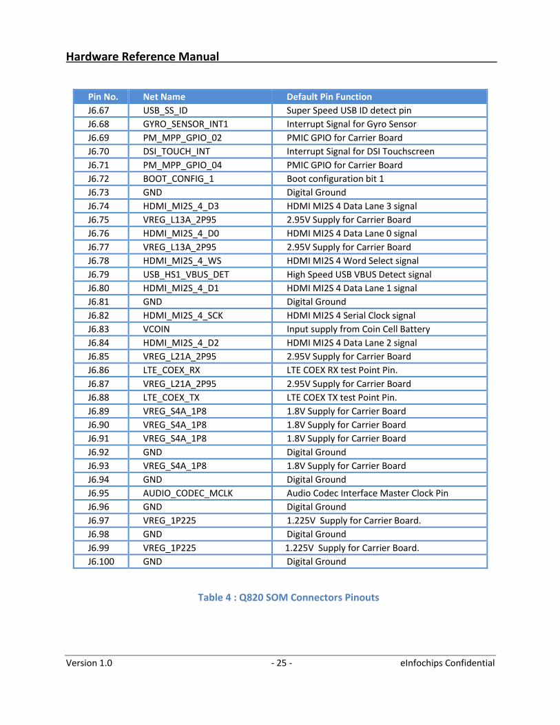
Table 4 : Q820 SOM Connectors Pinouts .................................................................................................... 25
Table 5 : MIPI CSI0 Pinouts ......................................................................................................................... 26
Table 6 : MIPI CSI1 Pinouts ......................................................................................................................... 26
Table 7 : MIPI CSI2 Pinouts ......................................................................................................................... 27
Table 8 : Dedicated I2C Signals ................................................................................................................... 27
Table 9 : MIPI DSI0 Pinouts ......................................................................................................................... 27
Table 10 : MIPI DSI1 Pinouts ....................................................................................................................... 28
Table 11 : HDMI Pinouts ............................................................................................................................. 28
Table 12 : I2S Interface Pinouts .................................................................................................................. 29
Table 13 : PCM Interface Pinouts ................................................................................................................ 29
Table 14 : USB 2.0 Interface Pinouts ........................................................................................................... 30
Table 15 : USB 3.0 Interface Pinouts ........................................................................................................... 30
Table 16 : JTAG Interface Pinouts ............................................................................................................... 31
Table 17 : SD Card Interface Pinouts........................................................................................................... 31
Table 18 : BLSP Interface Pinouts ............................................................................................................... 32
Table 19 : PCIe Interface Pinouts ................................................................................................................ 33
Hardware Reference Manual
Version 1.0 - v - eInfochips Confidential
Table 20 : SSC Interface Pinouts ................................................................................................................. 33
Table 21 : PMIC GPIOs................................................................................................................................. 33
Table 22 : Boot Configurations ................................................................................................................... 34
Table 23 : Power Pins .................................................................................................................................. 37
Table 24 : Absolute Maximum Ratings ....................................................................................................... 37
Table 25 : Operating Conditions ................................................................................................................. 37
Hardware Reference Manual
Version 1.0 - 6 - eInfochips Confidential
1 Document Details
1.1 Document History
Versio
n
Author Reviewer Approver Description Of
Changes Name Date Name Review
Date
Name Date
Releas
e 1.0
eInfochips 22-March-16 eInfochips 27-March-16 eInfochips 27-March-16 Initial release
Releas
e 1.1
eInfochips 30-May-17 eInfochips 12-Jun-17 eInfochips 12-Jun-17 Release update
Table 1: Document History
1.2 Definition, Acronyms and Abbreviations
Definition/Acronym/Abbreviation Description
SOM System On Module
BLE Bluetooth Low Energy
BOM Bill of Material
Bpp Bits Per Pixel
BT Bluetooth
CPU Central Processing Unit
CSI Camera Serial Interface
DC Direct Current
DDR Double Data Rate
DMIPS Dhrystone MIPS
Hardware Reference Manual
Version 1.0 - 7 - eInfochips Confidential
DSI Display Serial Interface
eI eInfochips
GB Giga Byte
GPIO General Purpose Interface
GPS Global Positioning System
HD High Definition
HDMI High Definition Multimedia Interface
HSIC High-speed Serial Interface Connect
I/O Input Output
I2C Inter-Integrated Circuit
IC Integrated Circuit
Inc. Incorporated
JTAG Joint Test Application Group
KB Kilo Byte
LAN Local Area Network
LNA Low Noise Amplifier
LPDDR Lower Power DDR
MB Mega Byte
Mbps Mega Bits Per Second
MIPI Mobile protocol working Alliance (not an Acronym)
MIPS Million Instruction Per Second
MISO Master In Slave Out
Mm Millimeter
MMC Multi Media Card
Hardware Reference Manual
Version 1.0 - 8 - eInfochips Confidential
MOSI Master Out Slave In
MP Mega Pixel
MPP Multipurpose Pins
OTG On The Go
PCIe Peripheral Component Interface – Express
PLL Phase Loop Locked
PMIC Power Management IC
RAM Random Access Memory
RF Radio Frequency
RH Relative Humidity
RoHS Restriction of Hazardous Substances
Rx Receive
SATA Serial
SATA Serial Advance Technology Attachment
SiP System In Package
SMPS Switched Mode Power Supply
SOM System On Module
SPI Serial peripheral Interface
Tx Transmit
UART Universal Asynchronous Interface
USB Universal Serial Bus
VCO Voltage Controlled Oscillator
WLAN Wireless LAN
Table 2 : Definition, Acronyms and Abbreviations
Hardware Reference Manual
Version 1.0 - 9 - eInfochips Confidential
1.3 References
No. Document Version Remarks
1 Q820_SOM Schematic File 1.0
2 Q820_SOM Layout File 1.0
Table 3 : References
Hardware Reference Manual
Version 1.0 - 10 - eInfochips Confidential
2 License Agreement
Your use of this document is subject to and governed by those terms and conditions in the eInfochips
Ltd. Purchase and Software License Agreement for the APQ8096 based development platform, which
you or the legal entity you represent, as the case may be, accepted and agreed to when purchasing a
820 development platform from eInfochips Ltd. (“Agreement”). You may use this document, which shall
be considered part of the defined term “Documentation” for purposes of the Agreement, solely in
support of your permitted use of the 820 development platform under the Agreement. Distribution of
this document is strictly prohibited without the express written permission of eInfochips Ltd. and its
respective licensors, which they can withhold, condition or delay in its sole discretion.
eInfochips is a trademark of eInfochips Ltd., registered in India, USA and other countries.
Qualcomm is a trademark of Qualcomm Inc., registered in the United States and other countries. Other
product and brand names used herein may be trademarks or registered trademarks of their respective
owners.
This document contains technical data that may be subject to U.S. and international export, re-export,
or transfer (“export”) laws. Diversion contrary to U.S. and international law is strictly prohibited.
Hardware Reference Manual
Version 1.0 - 11 - eInfochips Confidential
3 Preface This document provides an overview of the Q820 SOM design based on Qualcomm’s APQ8096 SoC. It
provides detailed information about the hardware components and associated software (Android 5.1.1
and Linaro Release 15.07).
Intended Audience This document is intended for technically qualified personnel. It is not intended for general audiences.
Intended Use The development platform supports a wide range of industry interfaces and offers a comprehensive
hardware and software design. It comes with Android 5.1.1 and Linaro 15.07 software packages and
sample demo applications for easy adaption.
This platform enables developers to evaluate and create solutions targeted at various market segments
while customers and OEMs can build their products based on these designs directly or with
customizations.
Hardware Reference Manual
Version 1.0 - 12 - eInfochips Confidential
4 Overview The Q820 SOM provides an ideal building block for simple integration with a wide range of products in
target markets requiring rich multimedia functionality, powerful graphics processing and video
capabilities, as well as high-processing power, in a compact, RoHS compliant, fan less, cost effective
SOM with low power consumption.
The Q820 SOM leverages cutting edge mobile computing for embedded and industrial product designs,
based on the Qualcomm Snapdragon™ 820 (APQ8096) quad Krait™ CPU, high performance Adreno 530
GPU and a dedicated DSP for advanced A/V processing.
The SOM is equipped with full range of interfaces available in the Qualcomm Snapdragon APQ8096 SoC,
which are routed to the three 100 pin Board to Board connector.
The APQ8096 SOM supports two operating system
- Linaro Kernel (15.07)
- Android 5.1.1
The 820 Development kit is based on Q820 SOM for the developers to quick start their application
development and is ideal for rapid prototyping of end product. With support for almost all the
peripherals, it reduces the design time of innovative applications and helps achieve early time to
market. With variety of peripherals, this kit is targeted for wide range of applications supporting bulk
storage, faster connectivity, higher through put and performance at lower power.
Hardware Reference Manual
Version 1.0 - 13 - eInfochips Confidential
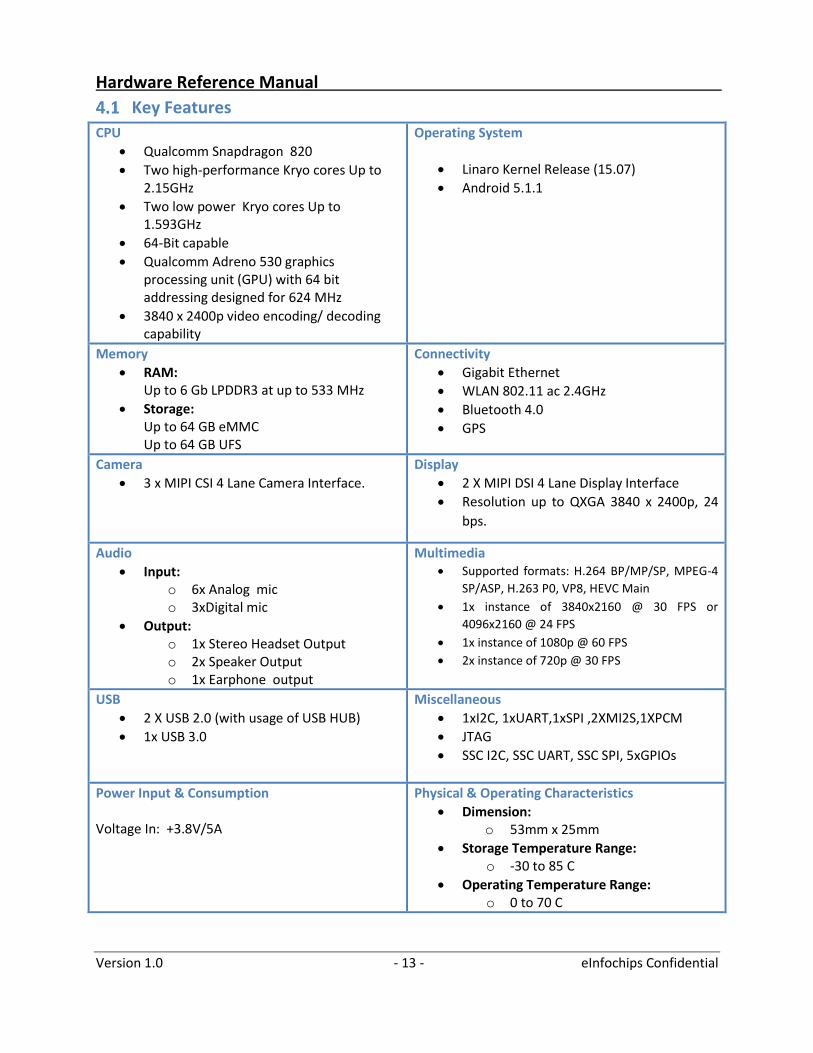
Key Features
CPU
Qualcomm Snapdragon 820
Two high-performance Kryo cores Up to 2.15GHz
Two low power Kryo cores Up to 1.593GHz
64-Bit capable
Qualcomm Adreno 530 graphics processing unit (GPU) with 64 bit addressing designed for 624 MHz
3840 x 2400p video encoding/ decoding capability
Operating System
Linaro Kernel Release (15.07)
Android 5.1.1
Memory
RAM: Up to 6 Gb LPDDR3 at up to 533 MHz
Storage: Up to 64 GB eMMC Up to 64 GB UFS
Connectivity
Gigabit Ethernet
WLAN 802.11 ac 2.4GHz
Bluetooth 4.0
GPS
Camera
3 x MIPI CSI 4 Lane Camera Interface.
Display
2 X MIPI DSI 4 Lane Display Interface
Resolution up to QXGA 3840 x 2400p, 24
bps.
Audio
Input: o 6x Analog mic o 3xDigital mic
Output: o 1x Stereo Headset Output o 2x Speaker Output o 1x Earphone output
Multimedia Supported formats: H.264 BP/MP/SP, MPEG-4
SP/ASP, H.263 P0, VP8, HEVC Main
1x instance of 3840x2160 @ 30 FPS or
4096x2160 @ 24 FPS
1x instance of 1080p @ 60 FPS
2x instance of 720p @ 30 FPS
USB
2 X USB 2.0 (with usage of USB HUB)
1x USB 3.0
Miscellaneous
1xI2C, 1xUART,1xSPI ,2XMI2S,1XPCM
JTAG
SSC I2C, SSC UART, SSC SPI, 5xGPIOs
Power Input & Consumption Voltage In: +3.8V/5A
Physical & Operating Characteristics
Dimension: o 53mm x 25mm
Storage Temperature Range: o -30 to 85 C
Operating Temperature Range: o 0 to 70 C
Hardware Reference Manual
Version 1.0 - 14 - eInfochips Confidential
Applications
The Q820 SOM is used in a wide range of products across many different target markets. Some of the
typical applications are:
Domestic Robot security & Surveillance
Biometric Access Control Systems
Human-machine interface
Portable medical
Machine vision
IoT
Medical
Robotic Application
Hardware Reference Manual
Version 1.0 - 15 - eInfochips Confidential
5 Getting Started Prerequisites Before power up the ERAGON 410 board for the first time user will need the following:
ERAGON 410 board.
The ERAGON 410 Boards compliant power supply.
A HDMI or DSI LCD Display that supports a resolution of minimmum720P/30Hz.
HDMI Bridge Board or LCD Bridge Board.
FFC Cable for connecting Bridge Board to the ERAGON 410 Board.
Standard Type-A HDMI-HDMI cable to connect the board to the Monitor.
USB Mouse & Keyboard.
Starting the board for the first time To start the board, follow these simple steps:
Step 1. Connect the ERAGON 410 Board to the HDMI Bridge Board or to the LCD Bridge Board using FFC cable provided along with kit.
Step 2. Connect the Standard HDMI Type A cable to the HDMI connector of HDMI Bridge board to the LCD Monitor which is compatible with the HDMI. User can also use the MIPI LCD Display for display purpose using the LCD Bridge Board.
Step 3. Connect the USB compatible keyboard and mouse to the USB connector of board. Step 4. Ensure that the boot switch SW5 is set to ‘000’, all in OFF position. Step 5. Connect the compatible power supply to power connector J15 on carrier board.
Once User plug the power supply into a power outlet the board will start the booting process, and User should see Android boot up image on screen. Please note that the first boot takes several minutes due to Androids initialization. Subsequent boot times should be faster. Note: If User uses the HDMI port, User has to connect both FFC cable, DSI Data FFC Cable & another for Audio Application. While using only LCD Bridge Board User has to connect only DSI Data FFC cable.
Hardware Reference Manual
Version 1.0 - 16 - eInfochips Confidential
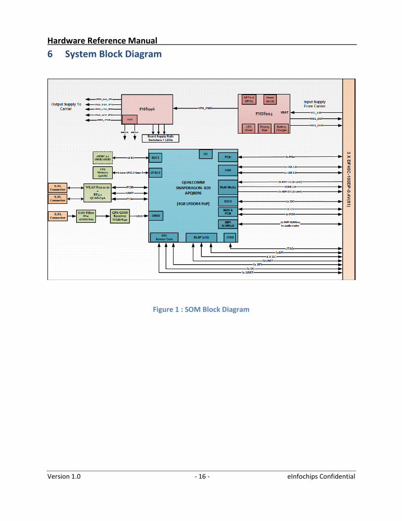
6 System Block Diagram
Figure 1 : SOM Block Diagram
Hardware Reference Manual
Version 1.0 - 17 - eInfochips Confidential
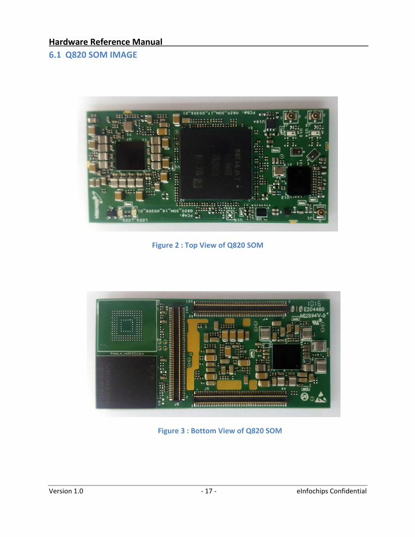
Q820 SOM IMAGE
Figure 2 : Top View of Q820 SOM
Figure 3 : Bottom View of Q820 SOM
Hardware Reference Manual
Version 1.0 - 18 - eInfochips Confidential
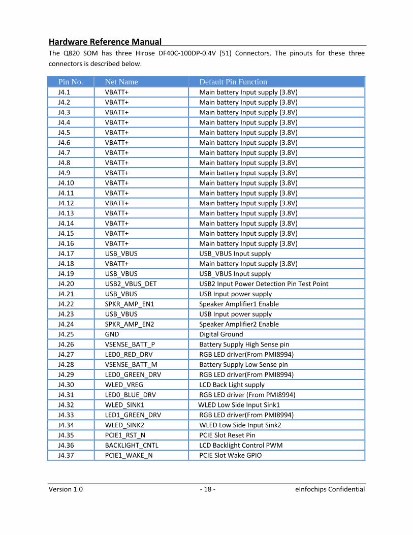
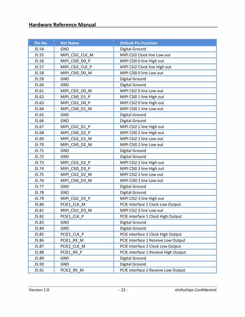
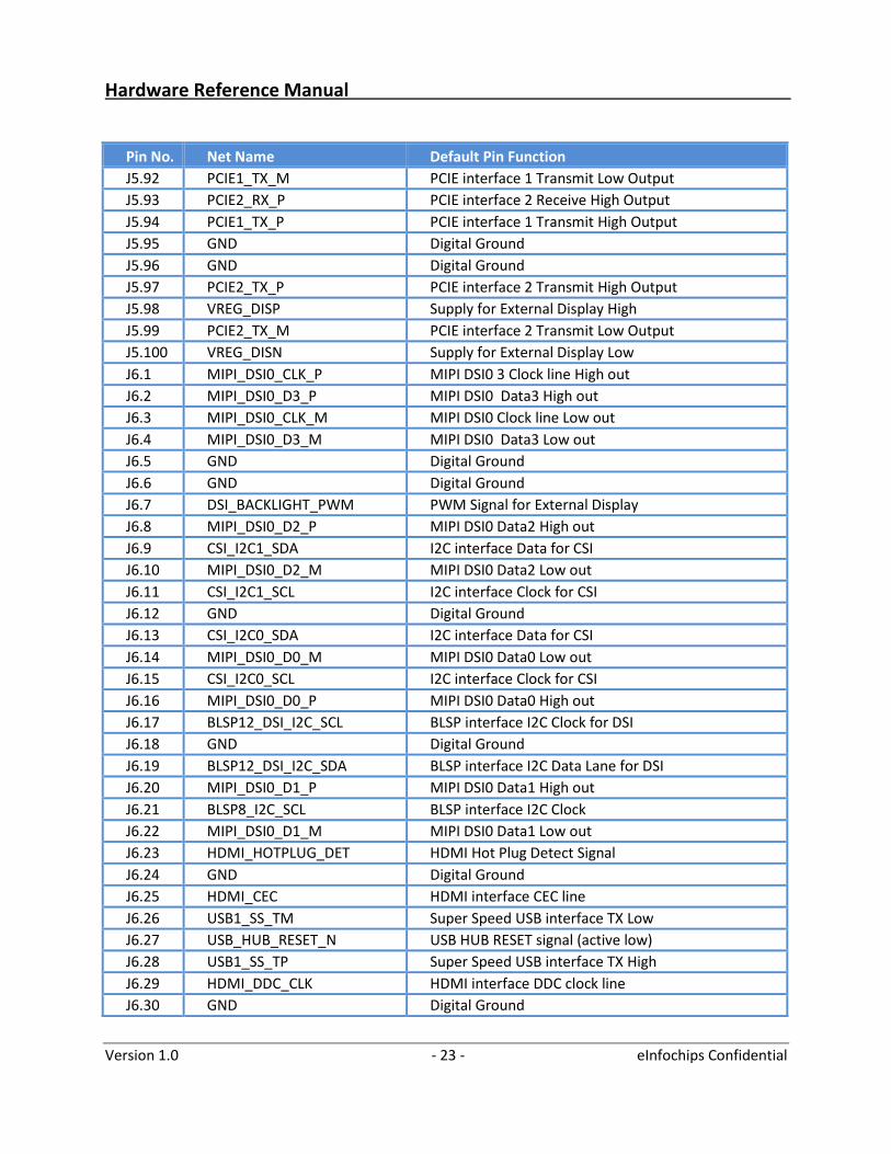
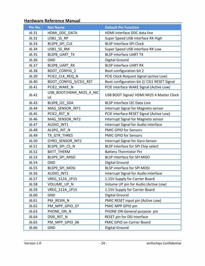
The Q820 SOM has three Hirose DF40C-100DP-0.4V (51) Connectors. The pinouts for these three
connectors is described below.
Pin No. Net Name Default Pin Function
J4.1 VBATT+ Main battery Input supply (3.8V)
J4.2 VBATT+ Main battery Input supply (3.8V)
J4.3 VBATT+ Main battery Input supply (3.8V)
J4.4 VBATT+ Main battery Input supply (3.8V)
J4.5 VBATT+ Main battery Input supply (3.8V)
J4.6 VBATT+ Main battery Input supply (3.8V)
J4.7 VBATT+ Main battery Input supply (3.8V)
J4.8 VBATT+ Main battery Input supply (3.8V)
J4.9 VBATT+ Main battery Input supply (3.8V)
J4.10 VBATT+ Main battery Input supply (3.8V)
J4.11 VBATT+ Main battery Input supply (3.8V)
J4.12 VBATT+ Main battery Input supply (3.8V)
J4.13 VBATT+ Main battery Input supply (3.8V)
J4.14 VBATT+ Main battery Input supply (3.8V)
J4.15 VBATT+ Main battery Input supply (3.8V)
J4.16 VBATT+ Main battery Input supply (3.8V)
J4.17 USB_VBUS USB_VBUS Input supply
J4.18 VBATT+ Main battery Input supply (3.8V)
J4.19 USB_VBUS USB_VBUS Input supply
J4.20 USB2_VBUS_DET USB2 Input Power Detection Pin Test Point
J4.21 USB_VBUS USB Input power supply
J4.22 SPKR_AMP_EN1 Speaker Amplifier1 Enable
J4.23 USB_VBUS USB Input power supply
J4.24 SPKR_AMP_EN2 Speaker Amplifier2 Enable
J4.25 GND Digital Ground
J4.26 VSENSE_BATT_P Battery Supply High Sense pin
J4.27 LED0_RED_DRV RGB LED driver(From PMI8994)
J4.28 VSENSE_BATT_M Battery Supply Low Sense pin
J4.29 LED0_GREEN_DRV RGB LED driver(From PMI8994)
J4.30 WLED_VREG LCD Back Light supply
J4.31 LED0_BLUE_DRV RGB LED driver (From PMI8994)
J4.32 WLED_SINK1 WLED Low Side Input Sink1
J4.33 LED1_GREEN_DRV RGB LED driver(From PMI8994)
J4.34 WLED_SINK2 WLED Low Side Input Sink2
J4.35 PCIE1_RST_N PCIE Slot Reset Pin
J4.36 BACKLIGHT_CNTL LCD Backlight Control PWM
J4.37 PCIE1_WAKE_N PCIE Slot Wake GPIO
Hardware Reference Manual
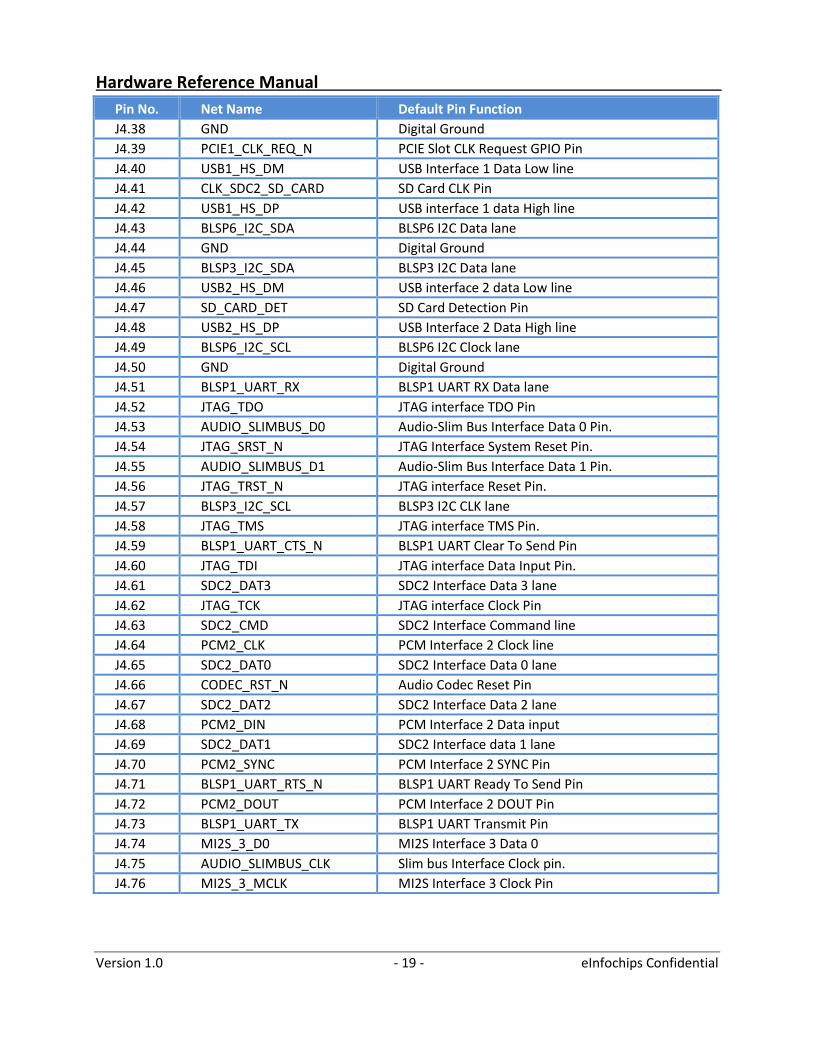
Version 1.0 - 19 - eInfochips Confidential
Pin No. Net Name Default Pin Function
J4.38 GND Digital Ground
J4.39 PCIE1_CLK_REQ_N PCIE Slot CLK Request GPIO Pin
J4.40 USB1_HS_DM USB Interface 1 Data Low line
J4.41 CLK_SDC2_SD_CARD SD Card CLK Pin
J4.42 USB1_HS_DP USB interface 1 data High line
J4.43 BLSP6_I2C_SDA BLSP6 I2C Data lane
J4.44 GND Digital Ground
J4.45 BLSP3_I2C_SDA BLSP3 I2C Data lane
J4.46 USB2_HS_DM USB interface 2 data Low line
J4.47 SD_CARD_DET SD Card Detection Pin
J4.48 USB2_HS_DP USB Interface 2 Data High line
J4.49 BLSP6_I2C_SCL BLSP6 I2C Clock lane
J4.50 GND Digital Ground
J4.51 BLSP1_UART_RX BLSP1 UART RX Data lane
J4.52 JTAG_TDO JTAG interface TDO Pin
J4.53 AUDIO_SLIMBUS_D0 Audio-Slim Bus Interface Data 0 Pin.
J4.54 JTAG_SRST_N JTAG Interface System Reset Pin.
J4.55 AUDIO_SLIMBUS_D1 Audio-Slim Bus Interface Data 1 Pin.
J4.56 JTAG_TRST_N JTAG interface Reset Pin.
J4.57 BLSP3_I2C_SCL BLSP3 I2C CLK lane
J4.58 JTAG_TMS JTAG interface TMS Pin.
J4.59 BLSP1_UART_CTS_N BLSP1 UART Clear To Send Pin
J4.60 JTAG_TDI JTAG interface Data Input Pin.
J4.61 SDC2_DAT3 SDC2 Interface Data 3 lane
J4.62 JTAG_TCK JTAG interface Clock Pin
J4.63 SDC2_CMD SDC2 Interface Command line
J4.64 PCM2_CLK PCM Interface 2 Clock line
J4.65 SDC2_DAT0 SDC2 Interface Data 0 lane
J4.66 CODEC_RST_N Audio Codec Reset Pin
J4.67 SDC2_DAT2 SDC2 Interface Data 2 lane
J4.68 PCM2_DIN PCM Interface 2 Data input
J4.69 SDC2_DAT1 SDC2 Interface data 1 lane
J4.70 PCM2_SYNC PCM Interface 2 SYNC Pin
J4.71 BLSP1_UART_RTS_N BLSP1 UART Ready To Send Pin
J4.72 PCM2_DOUT PCM Interface 2 DOUT Pin
J4.73 BLSP1_UART_TX BLSP1 UART Transmit Pin
J4.74 MI2S_3_D0 MI2S Interface 3 Data 0
J4.75 AUDIO_SLIMBUS_CLK Slim bus Interface Clock pin.
J4.76 MI2S_3_MCLK MI2S Interface 3 Clock Pin
Hardware Reference Manual
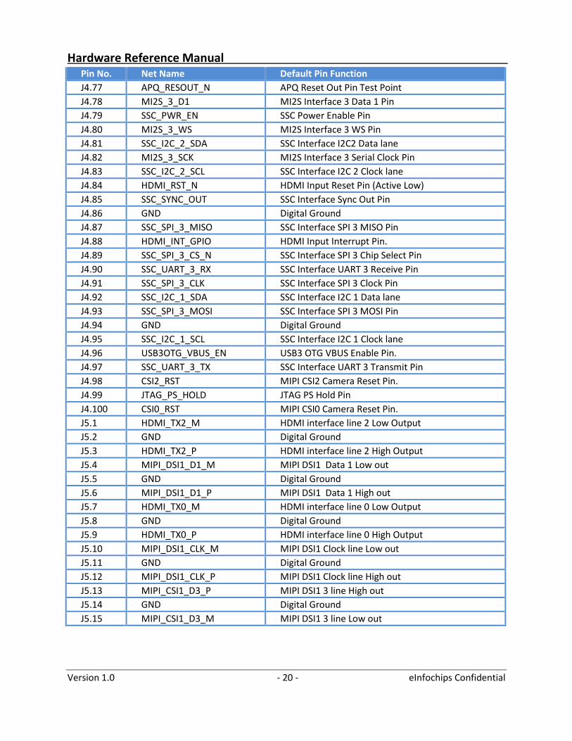
Version 1.0 - 20 - eInfochips Confidential
Pin No. Net Name Default Pin Function
J4.77 APQ_RESOUT_N APQ Reset Out Pin Test Point
J4.78 MI2S_3_D1 MI2S Interface 3 Data 1 Pin
J4.79 SSC_PWR_EN SSC Power Enable Pin
J4.80 MI2S_3_WS MI2S Interface 3 WS Pin
J4.81 SSC_I2C_2_SDA SSC Interface I2C2 Data lane
J4.82 MI2S_3_SCK MI2S Interface 3 Serial Clock Pin
J4.83 SSC_I2C_2_SCL SSC Interface I2C 2 Clock lane
J4.84 HDMI_RST_N HDMI Input Reset Pin (Active Low)
J4.85 SSC_SYNC_OUT SSC Interface Sync Out Pin
J4.86 GND Digital Ground
J4.87 SSC_SPI_3_MISO SSC Interface SPI 3 MISO Pin
J4.88 HDMI_INT_GPIO HDMI Input Interrupt Pin.
J4.89 SSC_SPI_3_CS_N SSC Interface SPI 3 Chip Select Pin
J4.90 SSC_UART_3_RX SSC Interface UART 3 Receive Pin
J4.91 SSC_SPI_3_CLK SSC Interface SPI 3 Clock Pin
J4.92 SSC_I2C_1_SDA SSC Interface I2C 1 Data lane
J4.93 SSC_SPI_3_MOSI SSC Interface SPI 3 MOSI Pin
J4.94 GND Digital Ground
J4.95 SSC_I2C_1_SCL SSC Interface I2C 1 Clock lane
J4.96 USB3OTG_VBUS_EN USB3 OTG VBUS Enable Pin.
J4.97 SSC_UART_3_TX SSC Interface UART 3 Transmit Pin
J4.98 CSI2_RST MIPI CSI2 Camera Reset Pin.
J4.99 JTAG_PS_HOLD JTAG PS Hold Pin
J4.100 CSI0_RST MIPI CSI0 Camera Reset Pin.
J5.1 HDMI_TX2_M HDMI interface line 2 Low Output
J5.2 GND Digital Ground
J5.3 HDMI_TX2_P HDMI interface line 2 High Output
J5.4 MIPI_DSI1_D1_M MIPI DSI1 Data 1 Low out
J5.5 GND Digital Ground
J5.6 MIPI_DSI1_D1_P MIPI DSI1 Data 1 High out
J5.7 HDMI_TX0_M HDMI interface line 0 Low Output
J5.8 GND Digital Ground
J5.9 HDMI_TX0_P HDMI interface line 0 High Output
J5.10 MIPI_DSI1_CLK_M MIPI DSI1 Clock line Low out
J5.11 GND Digital Ground
J5.12 MIPI_DSI1_CLK_P MIPI DSI1 Clock line High out
J5.13 MIPI_CSI1_D3_P MIPI DSI1 3 line High out
J5.14 GND Digital Ground
J5.15 MIPI_CSI1_D3_M MIPI DSI1 3 line Low out
Hardware Reference Manual
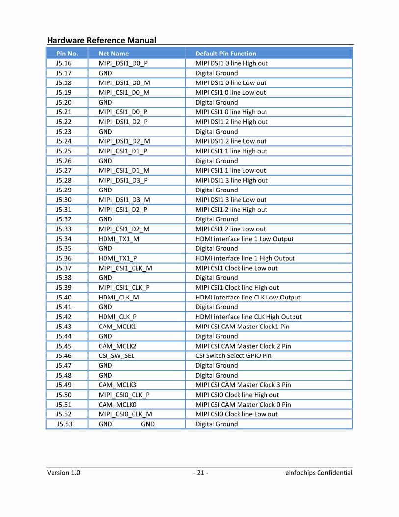
Version 1.0 - 21 - eInfochips Confidential
Pin No. Net Name Default Pin Function
J5.16 MIPI_DSI1_D0_P MIPI DSI1 0 line High out
J5.17 GND Digital Ground
J5.18 MIPI_DSI1_D0_M MIPI DSI1 0 line Low out
J5.19 MIPI_CSI1_D0_M MIPI CSI1 0 line Low out
J5.20 GND Digital Ground
J5.21 MIPI_CSI1_D0_P MIPI CSI1 0 line High out
J5.22 MIPI_DSI1_D2_P MIPI DSI1 2 line High out
J5.23 GND Digital Ground
J5.24 MIPI_DSI1_D2_M MIPI DSI1 2 line Low out
J5.25 MIPI_CSI1_D1_P MIPI CSI1 1 line High out
J5.26 GND Digital Ground
J5.27 MIPI_CSI1_D1_M MIPI CSI1 1 line Low out
J5.28 MIPI_DSI1_D3_P MIPI DSI1 3 line High out
J5.29 GND Digital Ground
J5.30 MIPI_DSI1_D3_M MIPI DSI1 3 line Low out
J5.31 MIPI_CSI1_D2_P MIPI CSI1 2 line High out
J5.32 GND Digital Ground
J5.33 MIPI_CSI1_D2_M MIPI CSI1 2 line Low out
J5.34 HDMI_TX1_M HDMI interface line 1 Low Output
J5.35 GND Digital Ground
J5.36 HDMI_TX1_P HDMI interface line 1 High Output
J5.37 MIPI_CSI1_CLK_M MIPI CSI1 Clock line Low out
J5.38 GND Digital Ground
J5.39 MIPI_CSI1_CLK_P MIPI CSI1 Clock line High out
J5.40 HDMI_CLK_M HDMI interface line CLK Low Output
J5.41 GND Digital Ground
J5.42 HDMI_CLK_P HDMI interface line CLK High Output
J5.43 CAM_MCLK1 MIPI CSI CAM Master Clock1 Pin
J5.44 GND Digital Ground
J5.45 CAM_MCLK2 MIPI CSI CAM Master Clock 2 Pin
J5.46 CSI_SW_SEL CSI Switch Select GPIO Pin
J5.47 GND Digital Ground
J5.48 GND Digital Ground
J5.49 CAM_MCLK3 MIPI CSI CAM Master Clock 3 Pin
J5.50 MIPI_CSI0_CLK_P MIPI CSI0 Clock line High out
J5.51 CAM_MCLK0 MIPI CSI CAM Master Clock 0 Pin
J5.52 MIPI_CSI0_CLK_M MIPI CSI0 Clock line Low out
J5.53 GND
GND Digital Ground
Hardware Reference Manual
Version 1.0 - 22 - eInfochips Confidential
Pin No. Net Name Default Pin Function
J5.54 GND Digital Ground
J5.55 MIPI_CSI2_CLK_M MIPI CSI2 Clock line Low out
J5.56 MIPI_CSI0_D0_P MIPI CSI0 0 line High out
J5.57 MIPI_CSI2_CLK_P MIPI CSI2 Clock line High out
J5.58 MIPI_CSI0_D0_M MIPI CSI0 0 line Low out
J5.59 GND Digital Ground
J5.60 GND Digital Ground
J5.61 MIPI_CSI2_D0_M MIPI CSI2 0 line Low out
J5.62 MIPI_CSI0_D1_P MIPI CSI0 1 line High out
J5.63 MIPI_CSI2_D0_P MIPI CSI2 0 line High out
J5.64 MIPI_CSI0_D1_M MIPI CSI0 1 line Low out
J5.65 GND Digital Ground
J5.66 GND Digital Ground
J5.67 MIPI_CSI2_D1_P MIPI CSI2 1 line High out
J5.68 MIPI_CSI0_D2_P MIPI CSI0 2 line High out
J5.69 MIPI_CSI2_D1_M MIPI CSI2 1 line Low out
J5.70 MIPI_CSI0_D2_M MIPI CSI0 2 line Low out
J5.71 GND Digital Ground
J5.72 GND Digital Ground
J5.73 MIPI_CSI2_D2_P MIPI CSI2 2 line High out
J5.74 MIPI_CSI0_D3_P MIPI CSI0 3 line High out
J5.75 MIPI_CSI2_D2_M MIPI CSI2 2 line Low out
J5.76 MIPI_CSI0_D3_M MIPI CSI0 3 line Low out
J5.77 GND Digital Ground
J5.78 GND Digital Ground
J5.79 MIPI_CSI2_D3_P MIPI CSI2 3 line High out
J5.80 PCIE1_CLK_M PCIE interface 1 Clock Low Output
J5.81 MIPI_CSI2_D3_M MIPI CSI2 3 line Low out
J5.82 PCIE1_CLK_P PCIE interface 1 Clock High Output
J5.83 GND Digital Ground
J5.84 GND Digital Ground
J5.85 PCIE2_CLK_P PCIE interface 2 Clock High Output
J5.86 PCIE1_RX_M PCIE interface 1 Receive Low Output
J5.87 PCIE2_CLK_M PCIE Interface 2 Clock Low Output
J5.88 PCIE1_RX_P PCIE interface 1 Receive High Output
J5.89 GND Digital Ground
J5.90 GND Digital Ground
J5.91 PCIE2_RX_M PCIE interface 2 Receive Low Output
Hardware Reference Manual
Version 1.0 - 23 - eInfochips Confidential
Pin No. Net Name Default Pin Function
J5.92 PCIE1_TX_M PCIE interface 1 Transmit Low Output
J5.93 PCIE2_RX_P PCIE interface 2 Receive High Output
J5.94 PCIE1_TX_P PCIE interface 1 Transmit High Output
J5.95 GND Digital Ground
J5.96 GND Digital Ground
J5.97 PCIE2_TX_P PCIE interface 2 Transmit High Output
J5.98 VREG_DISP Supply for External Display High
J5.99 PCIE2_TX_M PCIE interface 2 Transmit Low Output
J5.100 VREG_DISN Supply for External Display Low
J6.1 MIPI_DSI0_CLK_P MIPI DSI0 3 Clock line High out
J6.2 MIPI_DSI0_D3_P MIPI DSI0 Data3 High out
J6.3 MIPI_DSI0_CLK_M MIPI DSI0 Clock line Low out
J6.4 MIPI_DSI0_D3_M MIPI DSI0 Data3 Low out
J6.5 GND Digital Ground
J6.6 GND Digital Ground
J6.7 DSI_BACKLIGHT_PWM PWM Signal for External Display
J6.8 MIPI_DSI0_D2_P MIPI DSI0 Data2 High out
J6.9 CSI_I2C1_SDA I2C interface Data for CSI
J6.10 MIPI_DSI0_D2_M MIPI DSI0 Data2 Low out
J6.11 CSI_I2C1_SCL I2C interface Clock for CSI
J6.12 GND Digital Ground
J6.13 CSI_I2C0_SDA I2C interface Data for CSI
J6.14 MIPI_DSI0_D0_M MIPI DSI0 Data0 Low out
J6.15 CSI_I2C0_SCL I2C interface Clock for CSI
J6.16 MIPI_DSI0_D0_P MIPI DSI0 Data0 High out
J6.17 BLSP12_DSI_I2C_SCL BLSP interface I2C Clock for DSI
J6.18 GND Digital Ground
J6.19 BLSP12_DSI_I2C_SDA BLSP interface I2C Data Lane for DSI
J6.20 MIPI_DSI0_D1_P MIPI DSI0 Data1 High out
J6.21 BLSP8_I2C_SCL BLSP interface I2C Clock
J6.22 MIPI_DSI0_D1_M MIPI DSI0 Data1 Low out
J6.23 HDMI_HOTPLUG_DET HDMI Hot Plug Detect Signal
J6.24 GND Digital Ground
J6.25 HDMI_CEC HDMI interface CEC line
J6.26 USB1_SS_TM Super Speed USB interface TX Low
J6.27 USB_HUB_RESET_N USB HUB RESET signal (active low)
J6.28 USB1_SS_TP Super Speed USB interface TX High
J6.29 HDMI_DDC_CLK HDMI interface DDC clock line
J6.30 GND Digital Ground
Hardware Reference Manual
Version 1.0 - 24 - eInfochips Confidential
Pin No. Net Name Default Pin Function
J6.31 HDMI_DDC_DATA HDMI interface DDC data line
J6.32 USB1_SS_RP Super Speed USB interface RX High
J6.33 BLSP9_SPI_CLK BLSP interface SPI Clock
J6.34 USB1_SS_RM Super Speed USB interface RX Low
J6.35 BLSP8_UART_TX BLSP interface UART TX
J6.36 GND Digital Ground
J6.37 BLSP8_UART_RX BLSP interface UART RX
J6.38 BOOT_CONFIG_2 Boot configuration bit 2
J6.39 PCIE2_CLK_REQ_N PCIE Clock Request Signal (active Low)
J6.40 BOOT_CONFIG_3/CSI1_RST Boot configuration bit 2/ CSI1 RESET Signal
J6.41 PCIE2_WAKE_N PCIE interface WAKE Signal (Active Low)
J6.42 USB_BOOT/HDMI_MI2S_4_MCLK
USB BOOT Signal/ HDMI MI2S 4 Master Clock
J6.43 BLSP8_I2C_SDA BLSP interface I2C Data Line
J6.44 MAG_SENSOR_INT1 Interrupt Signal for Magneto sensor
J6.45 PCIE2_RST_N PCIE interface RESET Signal (Active Low)
J6.46 MAG_SENSOR_INT2 Interrupt Signal for Magneto sensor
J6.47 AUDIO_INT1 Interrupt Signal for Audio interface
J6.48 ALSPG_INT_N PMIC GPIO for Sensors
J6.49 TX_GTR_THRES PMIC GPIO for Sensors
J6.50 GYRO_SENSOR_INT2 Interrupt Signal for Gyro Sensor
J6.51 BLSP9_SPI_CS_N BLSP interface for SPI Chip select
J6.52 BATT_THERM Battery Thermistor Pin
J6.53 BLSP9_SPI_MISO BLSP interface for SPI MISO
J6.54 GND Digital Ground
J6.55 BLSP9_SPI_MOSI BLSP interface for SPI MOSI
J6.56 AUDIO_INT2 Interrupt Signal for Audio interface
J6.57 VREG_S12A_1P15 1.15V Supply for Carrier Board
J6.58 VOLUME_UP_N Volume UP pin for Audio (Active Low)
J6.59 VREG_S12A_1P15 1.15V Supply for Carrier Board
J6.60 GND Digital Ground
J6.61 PM_RESIN_N PMIC RESET input pin (Active Low)
J6.62 PM_MPP_GPIO_07 PMIC MPP GPIO pin
J6.63 PHONE_ON_N PHONE ON General purpose pin
J6.64 DSI0_RST_N RESET pin for DSI interface
J6.65 PM_MPP_GPIO_06 PMIC GPIO on Carrier Board
J6.66 GND Digital Ground
Hardware Reference Manual
Version 1.0 - 25 - eInfochips Confidential
Pin No. Net Name Default Pin Function
J6.67 USB_SS_ID Super Speed USB ID detect pin
J6.68 GYRO_SENSOR_INT1 Interrupt Signal for Gyro Sensor
J6.69 PM_MPP_GPIO_02 PMIC GPIO for Carrier Board
J6.70 DSI_TOUCH_INT Interrupt Signal for DSI Touchscreen
J6.71 PM_MPP_GPIO_04 PMIC GPIO for Carrier Board
J6.72 BOOT_CONFIG_1 Boot configuration bit 1
J6.73 GND Digital Ground
J6.74 HDMI_MI2S_4_D3 HDMI MI2S 4 Data Lane 3 signal
J6.75 VREG_L13A_2P95 2.95V Supply for Carrier Board
J6.76 HDMI_MI2S_4_D0 HDMI MI2S 4 Data Lane 0 signal
J6.77 VREG_L13A_2P95 2.95V Supply for Carrier Board
J6.78 HDMI_MI2S_4_WS HDMI MI2S 4 Word Select signal
J6.79 USB_HS1_VBUS_DET High Speed USB VBUS Detect signal
J6.80 HDMI_MI2S_4_D1 HDMI MI2S 4 Data Lane 1 signal
J6.81 GND Digital Ground
J6.82 HDMI_MI2S_4_SCK HDMI MI2S 4 Serial Clock signal
J6.83 VCOIN Input supply from Coin Cell Battery
J6.84 HDMI_MI2S_4_D2 HDMI MI2S 4 Data Lane 2 signal
J6.85 VREG_L21A_2P95 2.95V Supply for Carrier Board
J6.86 LTE_COEX_RX LTE COEX RX test Point Pin.
J6.87 VREG_L21A_2P95 2.95V Supply for Carrier Board
J6.88 LTE_COEX_TX LTE COEX TX test Point Pin.
J6.89 VREG_S4A_1P8 1.8V Supply for Carrier Board
J6.90 VREG_S4A_1P8 1.8V Supply for Carrier Board
J6.91 VREG_S4A_1P8 1.8V Supply for Carrier Board
J6.92 GND Digital Ground
J6.93 VREG_S4A_1P8 1.8V Supply for Carrier Board
J6.94 GND Digital Ground
J6.95 AUDIO_CODEC_MCLK Audio Codec Interface Master Clock Pin
J6.96 GND Digital Ground
J6.97 VREG_1P225 1.225V Supply for Carrier Board.
J6.98 GND Digital Ground
J6.99 VREG_1P225 1.225V Supply for Carrier Board.
J6.100 GND Digital Ground
Table 4 : Q820 SOM Connectors Pinouts
Hardware Reference Manual
Version 1.0 - 26 - eInfochips Confidential
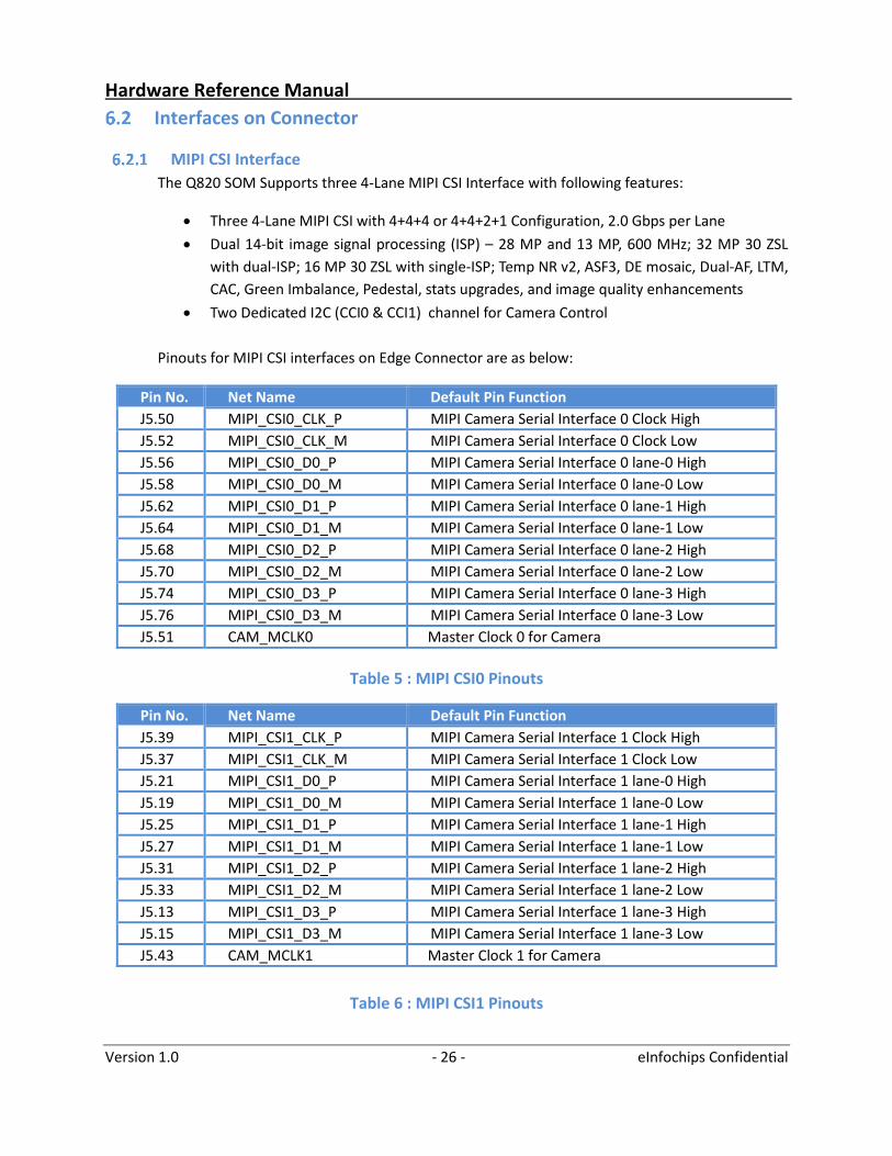
Interfaces on Connector
MIPI CSI Interface
The Q820 SOM Supports three 4-Lane MIPI CSI Interface with following features:
Three 4-Lane MIPI CSI with 4+4+4 or 4+4+2+1 Configuration, 2.0 Gbps per Lane
Dual 14-bit image signal processing (ISP) – 28 MP and 13 MP, 600 MHz; 32 MP 30 ZSL
with dual-ISP; 16 MP 30 ZSL with single-ISP; Temp NR v2, ASF3, DE mosaic, Dual-AF, LTM,
CAC, Green Imbalance, Pedestal, stats upgrades, and image quality enhancements
Two Dedicated I2C (CCI0 & CCI1) channel for Camera Control
Pinouts for MIPI CSI interfaces on Edge Connector are as below:
Pin No. Net Name Default Pin Function
J5.50 MIPI_CSI0_CLK_P MIPI Camera Serial Interface 0 Clock High
J5.52 MIPI_CSI0_CLK_M MIPI Camera Serial Interface 0 Clock Low
J5.56 MIPI_CSI0_D0_P MIPI Camera Serial Interface 0 lane-0 High
J5.58 MIPI_CSI0_D0_M MIPI Camera Serial Interface 0 lane-0 Low
J5.62 MIPI_CSI0_D1_P MIPI Camera Serial Interface 0 lane-1 High
J5.64 MIPI_CSI0_D1_M MIPI Camera Serial Interface 0 lane-1 Low
J5.68 MIPI_CSI0_D2_P MIPI Camera Serial Interface 0 lane-2 High
J5.70 MIPI_CSI0_D2_M MIPI Camera Serial Interface 0 lane-2 Low
J5.74 MIPI_CSI0_D3_P MIPI Camera Serial Interface 0 lane-3 High
J5.76 MIPI_CSI0_D3_M MIPI Camera Serial Interface 0 lane-3 Low
J5.51 CAM_MCLK0 Master Clock 0 for Camera
Table 5 : MIPI CSI0 Pinouts
Pin No. Net Name Default Pin Function
J5.39 MIPI_CSI1_CLK_P MIPI Camera Serial Interface 1 Clock High
J5.37 MIPI_CSI1_CLK_M MIPI Camera Serial Interface 1 Clock Low
J5.21 MIPI_CSI1_D0_P MIPI Camera Serial Interface 1 lane-0 High
J5.19 MIPI_CSI1_D0_M MIPI Camera Serial Interface 1 lane-0 Low
J5.25 MIPI_CSI1_D1_P MIPI Camera Serial Interface 1 lane-1 High
J5.27 MIPI_CSI1_D1_M MIPI Camera Serial Interface 1 lane-1 Low
J5.31 MIPI_CSI1_D2_P MIPI Camera Serial Interface 1 lane-2 High
J5.33 MIPI_CSI1_D2_M MIPI Camera Serial Interface 1 lane-2 Low
J5.13 MIPI_CSI1_D3_P MIPI Camera Serial Interface 1 lane-3 High
J5.15 MIPI_CSI1_D3_M MIPI Camera Serial Interface 1 lane-3 Low
J5.43 CAM_MCLK1 Master Clock 1 for Camera
Table 6 : MIPI CSI1 Pinouts
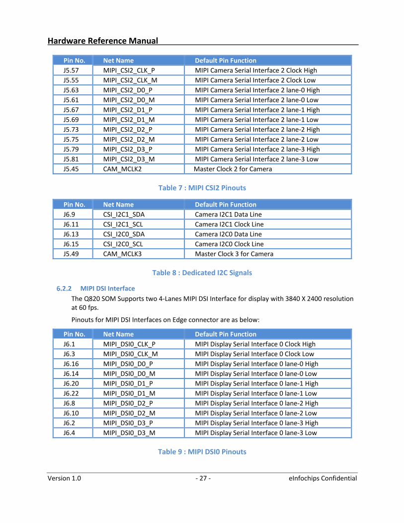
Hardware Reference Manual
Version 1.0 - 27 - eInfochips Confidential
Pin No. Net Name Default Pin Function
J5.57 MIPI_CSI2_CLK_P MIPI Camera Serial Interface 2 Clock High
J5.55 MIPI_CSI2_CLK_M MIPI Camera Serial Interface 2 Clock Low
J5.63 MIPI_CSI2_D0_P MIPI Camera Serial Interface 2 lane-0 High
J5.61 MIPI_CSI2_D0_M MIPI Camera Serial Interface 2 lane-0 Low
J5.67 MIPI_CSI2_D1_P MIPI Camera Serial Interface 2 lane-1 High
J5.69 MIPI_CSI2_D1_M MIPI Camera Serial Interface 2 lane-1 Low
J5.73 MIPI_CSI2_D2_P MIPI Camera Serial Interface 2 lane-2 High
J5.75 MIPI_CSI2_D2_M MIPI Camera Serial Interface 2 lane-2 Low
J5.79 MIPI_CSI2_D3_P MIPI Camera Serial Interface 2 lane-3 High
J5.81 MIPI_CSI2_D3_M MIPI Camera Serial Interface 2 lane-3 Low
J5.45 CAM_MCLK2 Master Clock 2 for Camera
Table 7 : MIPI CSI2 Pinouts
Pin No. Net Name Default Pin Function
J6.9 CSI_I2C1_SDA Camera I2C1 Data Line
J6.11 CSI_I2C1_SCL Camera I2C1 Clock Line
J6.13 CSI_I2C0_SDA Camera I2C0 Data Line
J6.15 CSI_I2C0_SCL Camera I2C0 Clock Line
J5.49 CAM_MCLK3 Master Clock 3 for Camera
Table 8 : Dedicated I2C Signals
MIPI DSI Interface
The Q820 SOM Supports two 4-Lanes MIPI DSI Interface for display with 3840 X 2400 resolution at 60 fps.
Pinouts for MIPI DSI Interfaces on Edge connector are as below:
Pin No. Net Name Default Pin Function
J6.1 MIPI_DSI0_CLK_P MIPI Display Serial Interface 0 Clock High
J6.3 MIPI_DSI0_CLK_M MIPI Display Serial Interface 0 Clock Low
J6.16 MIPI_DSI0_D0_P MIPI Display Serial Interface 0 lane-0 High
J6.14 MIPI_DSI0_D0_M MIPI Display Serial Interface 0 lane-0 Low
J6.20 MIPI_DSI0_D1_P MIPI Display Serial Interface 0 lane-1 High
J6.22 MIPI_DSI0_D1_M MIPI Display Serial Interface 0 lane-1 Low
J6.8 MIPI_DSI0_D2_P MIPI Display Serial Interface 0 lane-2 High
J6.10 MIPI_DSI0_D2_M MIPI Display Serial Interface 0 lane-2 Low
J6.2 MIPI_DSI0_D3_P MIPI Display Serial Interface 0 lane-3 High
J6.4 MIPI_DSI0_D3_M MIPI Display Serial Interface 0 lane-3 Low
Table 9 : MIPI DSI0 Pinouts
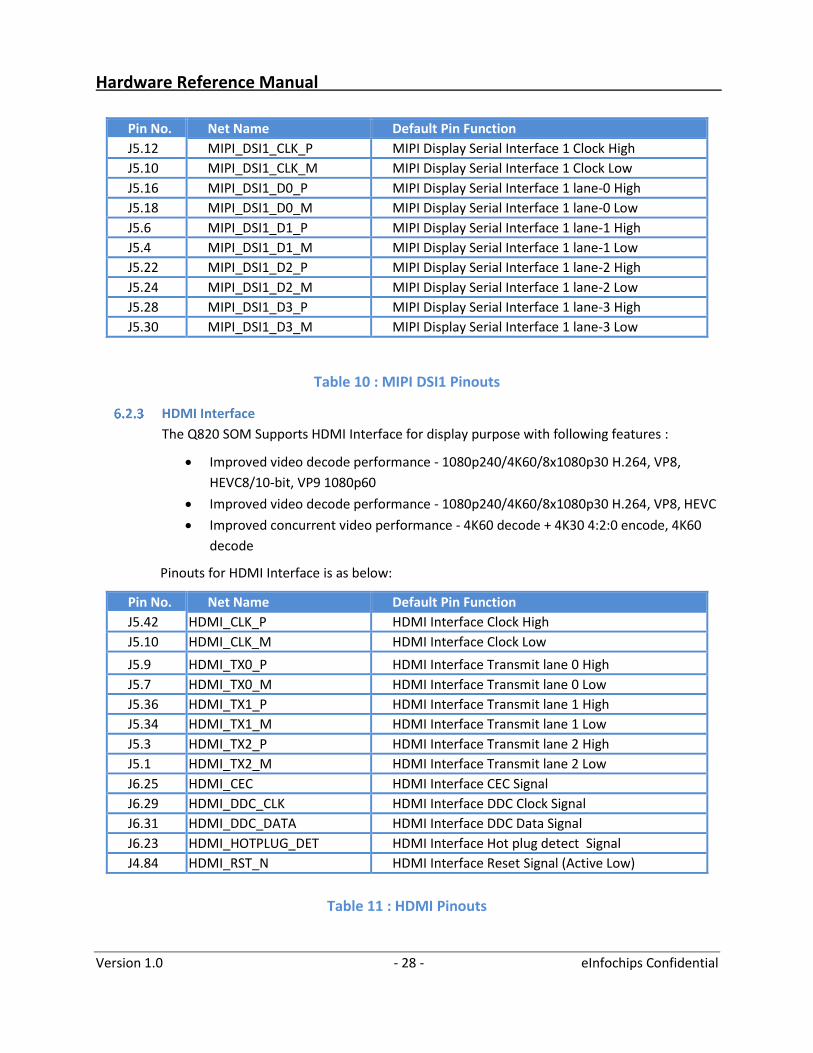
Hardware Reference Manual
Version 1.0 - 28 - eInfochips Confidential
Pin No. Net Name Default Pin Function
J5.12 MIPI_DSI1_CLK_P MIPI Display Serial Interface 1 Clock High
J5.10 MIPI_DSI1_CLK_M MIPI Display Serial Interface 1 Clock Low
J5.16 MIPI_DSI1_D0_P MIPI Display Serial Interface 1 lane-0 High
J5.18 MIPI_DSI1_D0_M MIPI Display Serial Interface 1 lane-0 Low
J5.6 MIPI_DSI1_D1_P MIPI Display Serial Interface 1 lane-1 High
J5.4 MIPI_DSI1_D1_M MIPI Display Serial Interface 1 lane-1 Low
J5.22 MIPI_DSI1_D2_P MIPI Display Serial Interface 1 lane-2 High
J5.24 MIPI_DSI1_D2_M MIPI Display Serial Interface 1 lane-2 Low
J5.28 MIPI_DSI1_D3_P MIPI Display Serial Interface 1 lane-3 High
J5.30 MIPI_DSI1_D3_M MIPI Display Serial Interface 1 lane-3 Low
Table 10 : MIPI DSI1 Pinouts
HDMI Interface
The Q820 SOM Supports HDMI Interface for display purpose with following features :
Improved video decode performance - 1080p240/4K60/8x1080p30 H.264, VP8,
HEVC8/10-bit, VP9 1080p60
Improved video decode performance - 1080p240/4K60/8x1080p30 H.264, VP8, HEVC
Improved concurrent video performance - 4K60 decode + 4K30 4:2:0 encode, 4K60
decode
Pinouts for HDMI Interface is as below:
Pin No. Net Name Default Pin Function
J5.42 HDMI_CLK_P HDMI Interface Clock High
J5.10 HDMI_CLK_M HDMI Interface Clock Low
J5.9 HDMI_TX0_P HDMI Interface Transmit lane 0 High
J5.7 HDMI_TX0_M HDMI Interface Transmit lane 0 Low
J5.36 HDMI_TX1_P HDMI Interface Transmit lane 1 High
J5.34 HDMI_TX1_M HDMI Interface Transmit lane 1 Low
J5.3 HDMI_TX2_P HDMI Interface Transmit lane 2 High
J5.1 HDMI_TX2_M HDMI Interface Transmit lane 2 Low
J6.25 HDMI_CEC HDMI Interface CEC Signal
J6.29 HDMI_DDC_CLK HDMI Interface DDC Clock Signal
J6.31 HDMI_DDC_DATA HDMI Interface DDC Data Signal
J6.23 HDMI_HOTPLUG_DET HDMI Interface Hot plug detect Signal
J4.84 HDMI_RST_N HDMI Interface Reset Signal (Active Low)
Table 11 : HDMI Pinouts
Hardware Reference Manual
Version 1.0 - 29 - eInfochips Confidential
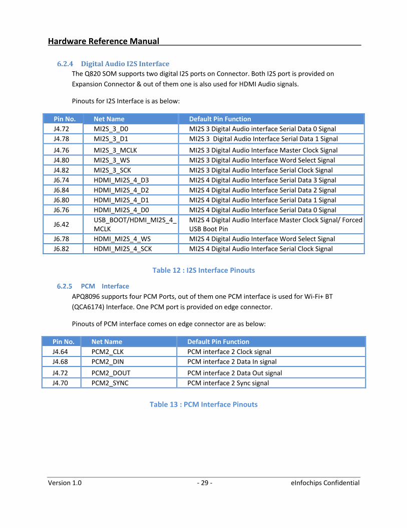
Digital Audio I2S Interface
The Q820 SOM supports two digital I2S ports on Connector. Both I2S port is provided on
Expansion Connector & out of them one is also used for HDMI Audio signals.
Pinouts for I2S Interface is as below:
Pin No. Net Name Default Pin Function
J4.72 MI2S_3_D0 MI2S 3 Digital Audio interface Serial Data 0 Signal
J4.78 MI2S_3_D1 MI2S 3 Digital Audio Interface Serial Data 1 Signal
J4.76 MI2S_3_MCLK MI2S 3 Digital Audio Interface Master Clock Signal
J4.80 MI2S_3_WS MI2S 3 Digital Audio Interface Word Select Signal
J4.82 MI2S_3_SCK MI2S 3 Digital Audio Interface Serial Clock Signal
J6.74 HDMI_MI2S_4_D3 MI2S 4 Digital Audio Interface Serial Data 3 Signal
J6.84 HDMI_MI2S_4_D2 MI2S 4 Digital Audio Interface Serial Data 2 Signal
J6.80 HDMI_MI2S_4_D1 MI2S 4 Digital Audio Interface Serial Data 1 Signal
J6.76 HDMI_MI2S_4_D0 MI2S 4 Digital Audio Interface Serial Data 0 Signal
J6.42 USB_BOOT/HDMI_MI2S_4_MCLK
MI2S 4 Digital Audio Interface Master Clock Signal/ Forced USB Boot Pin
J6.78 HDMI_MI2S_4_WS MI2S 4 Digital Audio Interface Word Select Signal
J6.82 HDMI_MI2S_4_SCK MI2S 4 Digital Audio Interface Serial Clock Signal
Table 12 : I2S Interface Pinouts
PCM Interface
APQ8096 supports four PCM Ports, out of them one PCM interface is used for Wi-Fi+ BT
(QCA6174) Interface. One PCM port is provided on edge connector.
Pinouts of PCM interface comes on edge connector are as below:
Pin No. Net Name Default Pin Function
J4.64 PCM2_CLK PCM interface 2 Clock signal
J4.68 PCM2_DIN PCM interface 2 Data In signal
J4.72 PCM2_DOUT PCM interface 2 Data Out signal
J4.70 PCM2_SYNC PCM interface 2 Sync signal
Table 13 : PCM Interface Pinouts
Hardware Reference Manual
Version 1.0 - 30 - eInfochips Confidential
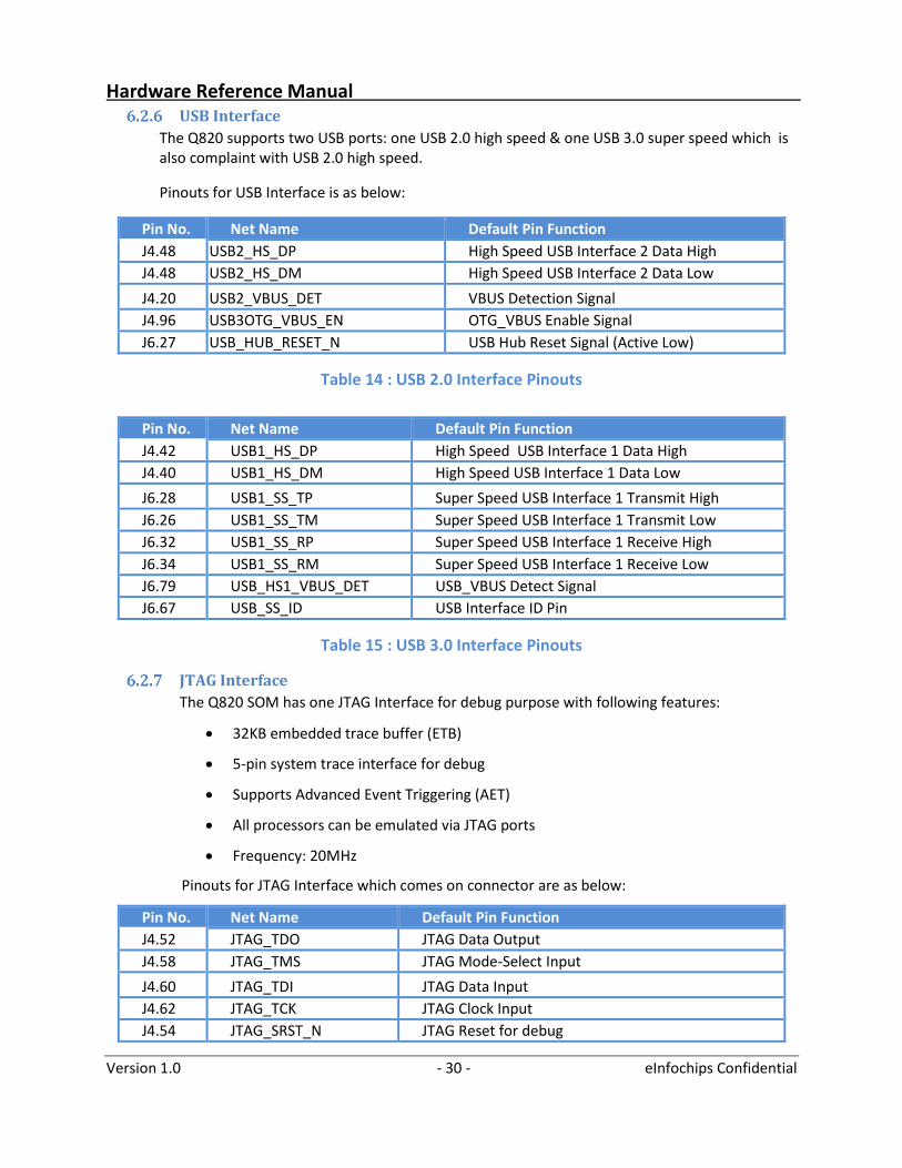
USB Interface
The Q820 supports two USB ports: one USB 2.0 high speed & one USB 3.0 super speed which is also complaint with USB 2.0 high speed.
Pinouts for USB Interface is as below:
Pin No. Net Name Default Pin Function
J4.48 USB2_HS_DP High Speed USB Interface 2 Data High
J4.48 USB2_HS_DM High Speed USB Interface 2 Data Low
J4.20 USB2_VBUS_DET VBUS Detection Signal
J4.96 USB3OTG_VBUS_EN OTG_VBUS Enable Signal
J6.27 USB_HUB_RESET_N USB Hub Reset Signal (Active Low)
Table 14 : USB 2.0 Interface Pinouts
Pin No. Net Name Default Pin Function
J4.42 USB1_HS_DP High Speed USB Interface 1 Data High
J4.40 USB1_HS_DM High Speed USB Interface 1 Data Low
J6.28 USB1_SS_TP Super Speed USB Interface 1 Transmit High
J6.26 USB1_SS_TM Super Speed USB Interface 1 Transmit Low
J6.32 USB1_SS_RP Super Speed USB Interface 1 Receive High
J6.34 USB1_SS_RM Super Speed USB Interface 1 Receive Low
J6.79 USB_HS1_VBUS_DET USB_VBUS Detect Signal
J6.67 USB_SS_ID USB Interface ID Pin
Table 15 : USB 3.0 Interface Pinouts
JTAG Interface
The Q820 SOM has one JTAG Interface for debug purpose with following features:
32KB embedded trace buffer (ETB)
5-pin system trace interface for debug
Supports Advanced Event Triggering (AET)
All processors can be emulated via JTAG ports
Frequency: 20MHz
Pinouts for JTAG Interface which comes on connector are as below:
Pin No. Net Name Default Pin Function
J4.52 JTAG_TDO JTAG Data Output
J4.58 JTAG_TMS JTAG Mode-Select Input
J4.60 JTAG_TDI JTAG Data Input
J4.62 JTAG_TCK JTAG Clock Input
J4.54 JTAG_SRST_N JTAG Reset for debug
Hardware Reference Manual
Version 1.0 - 31 - eInfochips Confidential
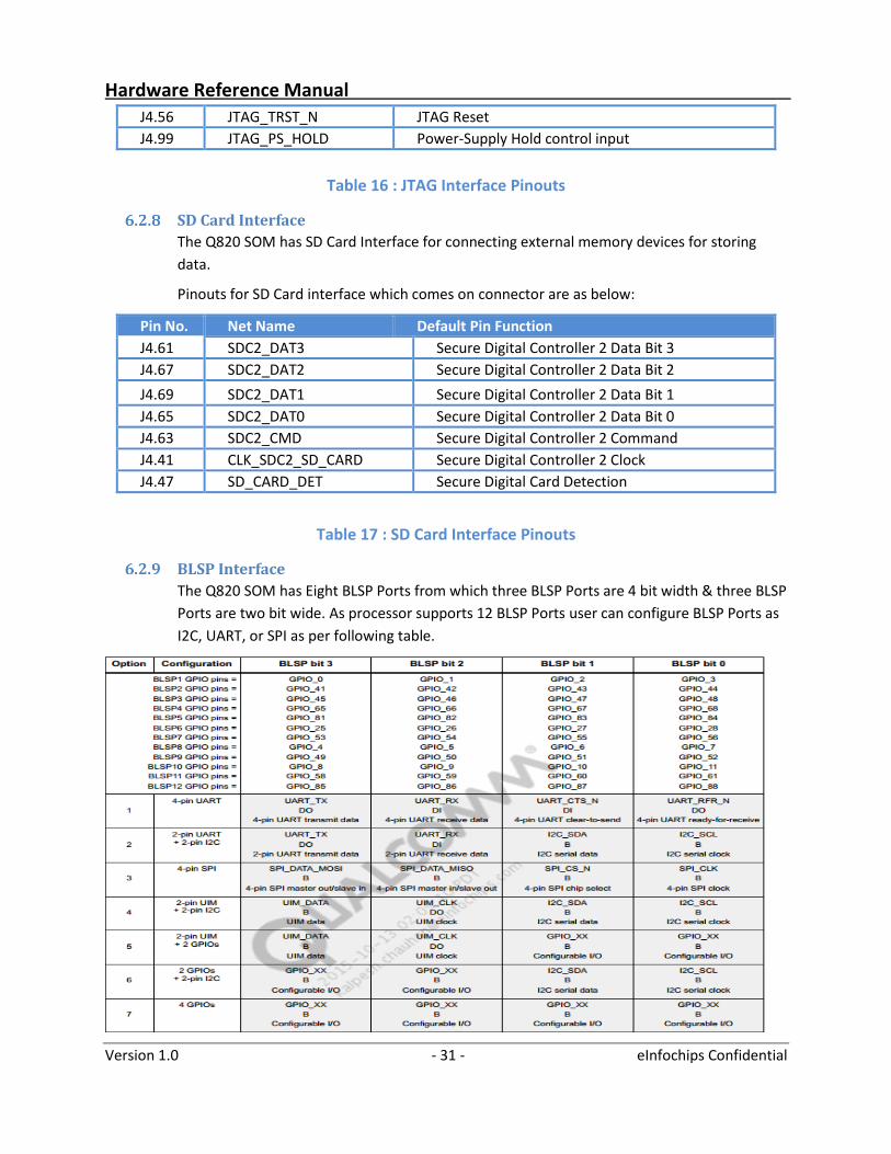
J4.56 JTAG_TRST_N JTAG Reset
J4.99 JTAG_PS_HOLD Power-Supply Hold control input
Table 16 : JTAG Interface Pinouts
SD Card Interface
The Q820 SOM has SD Card Interface for connecting external memory devices for storing
data.
Pinouts for SD Card interface which comes on connector are as below:
Pin No. Net Name Default Pin Function
J4.61 SDC2_DAT3 Secure Digital Controller 2 Data Bit 3
J4.67 SDC2_DAT2 Secure Digital Controller 2 Data Bit 2
J4.69 SDC2_DAT1 Secure Digital Controller 2 Data Bit 1
J4.65 SDC2_DAT0 Secure Digital Controller 2 Data Bit 0
J4.63 SDC2_CMD Secure Digital Controller 2 Command
J4.41 CLK_SDC2_SD_CARD Secure Digital Controller 2 Clock
J4.47 SD_CARD_DET Secure Digital Card Detection
Table 17 : SD Card Interface Pinouts
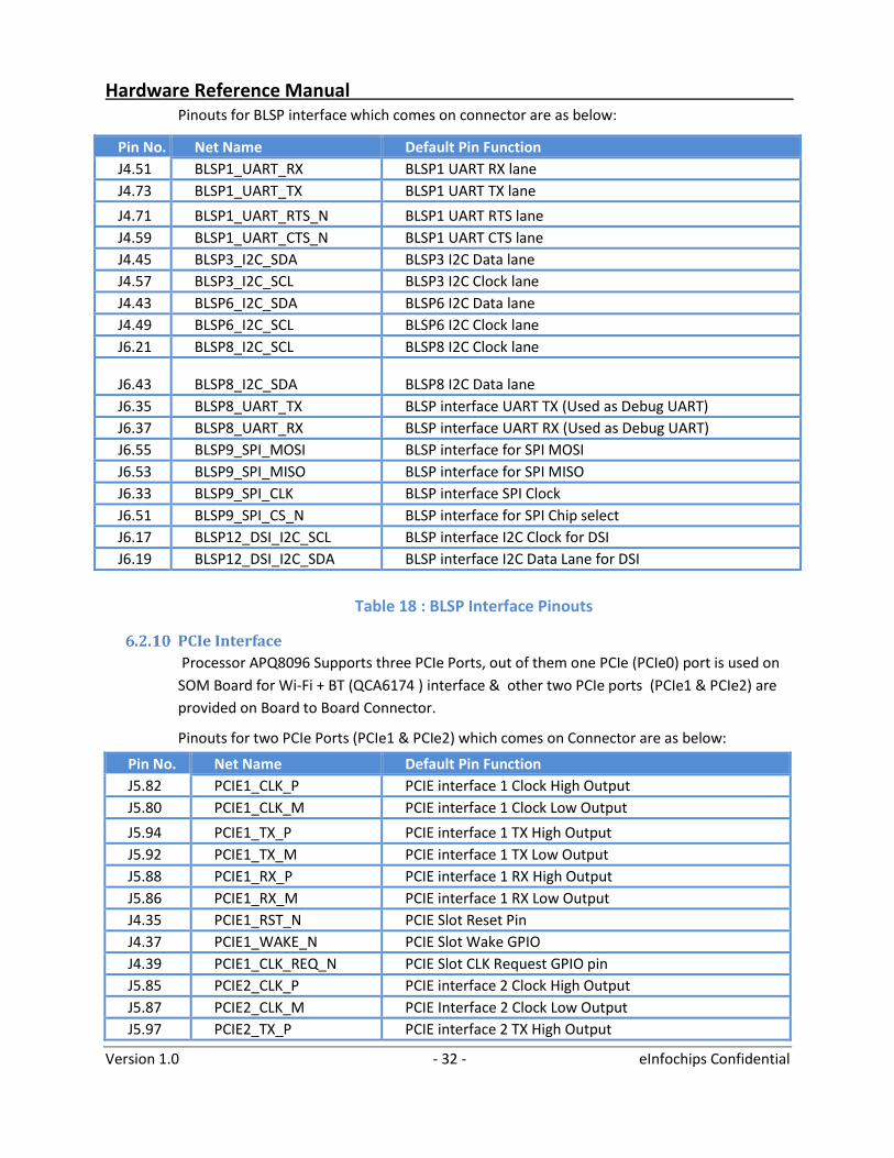
BLSP Interface
The Q820 SOM has Eight BLSP Ports from which three BLSP Ports are 4 bit width & three BLSP
Ports are two bit wide. As processor supports 12 BLSP Ports user can configure BLSP Ports as
I2C, UART, or SPI as per following table.
Hardware Reference Manual
Version 1.0 - 32 - eInfochips Confidential
Pinouts for BLSP interface which comes on connector are as below:
Pin No. Net Name Default Pin Function
J4.51 BLSP1_UART_RX BLSP1 UART RX lane
J4.73 BLSP1_UART_TX BLSP1 UART TX lane
J4.71 BLSP1_UART_RTS_N BLSP1 UART RTS lane
J4.59 BLSP1_UART_CTS_N BLSP1 UART CTS lane
J4.45 BLSP3_I2C_SDA BLSP3 I2C Data lane
J4.57 BLSP3_I2C_SCL BLSP3 I2C Clock lane
J4.43 BLSP6_I2C_SDA BLSP6 I2C Data lane
J4.49 BLSP6_I2C_SCL BLSP6 I2C Clock lane
J6.21 BLSP8_I2C_SCL BLSP8 I2C Clock lane
J6.43 BLSP8_I2C_SDA BLSP8 I2C Data lane
J6.35 BLSP8_UART_TX BLSP interface UART TX (Used as Debug UART)
J6.37 BLSP8_UART_RX BLSP interface UART RX (Used as Debug UART)
J6.55 BLSP9_SPI_MOSI BLSP interface for SPI MOSI
J6.53 BLSP9_SPI_MISO BLSP interface for SPI MISO
J6.33 BLSP9_SPI_CLK BLSP interface SPI Clock
J6.51 BLSP9_SPI_CS_N BLSP interface for SPI Chip select
J6.17 BLSP12_DSI_I2C_SCL BLSP interface I2C Clock for DSI
J6.19 BLSP12_DSI_I2C_SDA BLSP interface I2C Data Lane for DSI
Table 18 : BLSP Interface Pinouts
PCIe Interface
Processor APQ8096 Supports three PCIe Ports, out of them one PCIe (PCIe0) port is used on
SOM Board for Wi-Fi + BT (QCA6174 ) interface & other two PCIe ports (PCIe1 & PCIe2) are
provided on Board to Board Connector.
Pinouts for two PCIe Ports (PCIe1 & PCIe2) which comes on Connector are as below:
Pin No. Net Name Default Pin Function
J5.82 PCIE1_CLK_P PCIE interface 1 Clock High Output
J5.80 PCIE1_CLK_M PCIE interface 1 Clock Low Output
J5.94 PCIE1_TX_P PCIE interface 1 TX High Output
J5.92 PCIE1_TX_M PCIE interface 1 TX Low Output
J5.88 PCIE1_RX_P PCIE interface 1 RX High Output
J5.86 PCIE1_RX_M PCIE interface 1 RX Low Output
J4.35 PCIE1_RST_N PCIE Slot Reset Pin
J4.37 PCIE1_WAKE_N PCIE Slot Wake GPIO
J4.39 PCIE1_CLK_REQ_N PCIE Slot CLK Request GPIO pin
J5.85 PCIE2_CLK_P PCIE interface 2 Clock High Output
J5.87 PCIE2_CLK_M PCIE Interface 2 Clock Low Output
J5.97 PCIE2_TX_P PCIE interface 2 TX High Output
Hardware Reference Manual
Version 1.0 - 33 - eInfochips Confidential
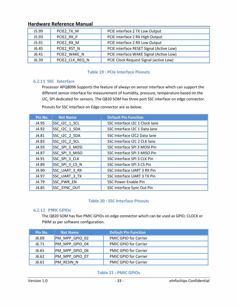
J5.99 PCIE2_TX_M PCIE interface 2 TX Low Output
J5.93 PCIE2_RX_P PCIE interface 2 RX High Output
J5.91 PCIE2_RX_M PCIE interface 2 RX Low Output
J6.45 PCIE2_RST_N PCIE interface RESET Signal (Active Low)
J6.41 PCIE2_WAKE_N PCIE interface WAKE Signal (Active Low)
J6.39 PCIE2_CLK_REQ_N PCIE Clock Request Signal (active Low)
Table 19 : PCIe Interface Pinouts
SSC Interface
Processor APQ8096 Supports the feature of always on sensor interface which can support the
different sensor interface for measurement of humidity, pressure, temperature based on the
I2C, SPI dedicated for sensors. The Q820 SOM has three port SSC interface on edge connector.
Pinouts for SSC Interface on Edge connector are as below:
Pin No. Net Name Default Pin Function
J4.95 SSC_I2C_1_SCL SSC Interface I2C 1 Clock lane
J4.92 SSC_I2C_1_SDA SSC Interface I2C 1 Data lane
J4.81 SSC_I2C_2_SDA SSC Interface I2C2 Data lane
J4.83 SSC_I2C_2_SCL SSC Interface I2C 2 CLK lane
J4.93 SSC_SPI_3_MOSI SSC Interface SPI 3 MOSI Pin
J4.87 SSC_SPI_3_MISO SSC Interface SPI 3 MISO Pin
J4.91 SSC_SPI_3_CLK SSC Interface SPI 3 CLK Pin
J4.89 SSC_SPI_3_CS_N SSC Interface SPI 3 CS Pin
J4.90 SSC_UART_3_RX SSC Interface UART 3 RX Pin
J4.97 SSC_UART_3_TX SSC Interface UART 3 TX Pin
J4.79 SSC_PWR_EN SSC Power Enable Pin
J4.85 SSC_SYNC_OUT SSC Interface Sync Out Pin
Table 20 : SSC Interface Pinouts
PMIC GPIOs
The Q820 SOM has five PMIC GPIOs on edge connector which can be used as GPIO, CLOCK or
PWM as per software configuration.
Pin No. Net Name Default Pin Function
J6.69 PM_MPP_GPIO_02 PMIC GPIO for Carrier
J6.71 PM_MPP_GPIO_04 PMIC GPIO for Carrier
J6.65 PM_MPP_GPIO_06 PMIC GPIO for Carrier
J6.62 PM_MPP_GPIO_07 PMIC GPIO for Carrier
J6.61 PM_RESIN_N PMIC GPIO for Carrier
Table 21 : PMIC GPIOs
Hardware Reference Manual
Version 1.0 - 34 - eInfochips Confidential
Wi-Fi + BT Interface
The Q820 SOM has low power QCA6174-1A Integrated Dual-Band 2 X 2 802.11ac WLAN +
Bluetooth 4.1 module. QCA6174 IC is integrated with processor using PCIe, UART & PCM
Interface .The QCA6174A is a single-die wireless local area network (WLAN) and Bluetooth
combo solution to support 2 × 2 multiple input, multiple output (MIMO) with two spatial
streams IEEE802.11 a/b/g/n/ac WLAN standards and Bluetooth 4.1 + HS enabling seamless
integration of WLAN/Bluetooth and low energy technology.
GPS Interface
The Q820 SOM supports GPS interface, for which the WGR7640 GPS receiver is integrated with
the Processor APQ8096. On the SOM board, it has X.FL. Connector by which one can connect the
active antenna externally for GPS application.
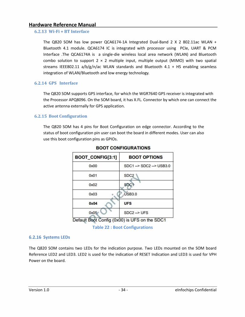
Boot Configuration
The Q820 SOM has 4 pins for Boot Configuration on edge connector. According to the
status of boot configuration pin user can boot the board in different modes. User can also
use this boot configuration pins as GPIOs.
Table 22 : Boot Configurations
Systems LEDs
The Q820 SOM contains two LEDs for the indication purpose. Two LEDs mounted on the SOM board
Reference LED2 and LED3. LED2 is used for the indication of RESET Indication and LED3 is used for VPH
Power on the board.
Hardware Reference Manual
Version 1.0 - 35 - eInfochips Confidential
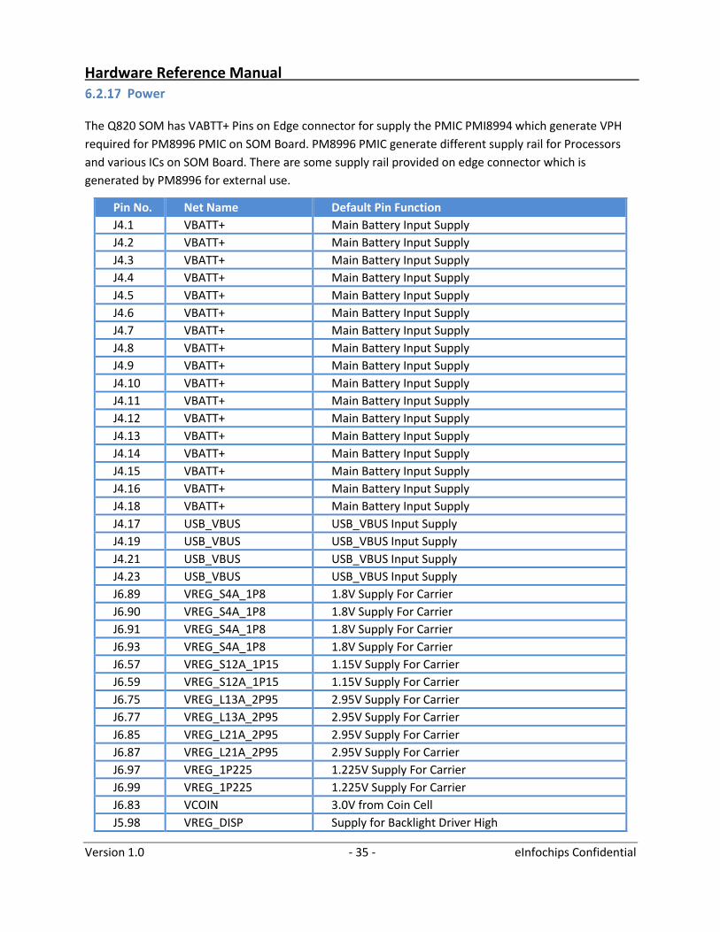
Power
The Q820 SOM has VABTT+ Pins on Edge connector for supply the PMIC PMI8994 which generate VPH
required for PM8996 PMIC on SOM Board. PM8996 PMIC generate different supply rail for Processors
and various ICs on SOM Board. There are some supply rail provided on edge connector which is
generated by PM8996 for external use.
Pin No. Net Name Default Pin Function
J4.1 VBATT+ Main Battery Input Supply
J4.2 VBATT+ Main Battery Input Supply
J4.3 VBATT+ Main Battery Input Supply
J4.4 VBATT+ Main Battery Input Supply
J4.5 VBATT+ Main Battery Input Supply
J4.6 VBATT+ Main Battery Input Supply
J4.7 VBATT+ Main Battery Input Supply
J4.8 VBATT+ Main Battery Input Supply
J4.9 VBATT+ Main Battery Input Supply
J4.10 VBATT+ Main Battery Input Supply
J4.11 VBATT+ Main Battery Input Supply
J4.12 VBATT+ Main Battery Input Supply
J4.13 VBATT+ Main Battery Input Supply
J4.14 VBATT+ Main Battery Input Supply
J4.15 VBATT+ Main Battery Input Supply
J4.16 VBATT+ Main Battery Input Supply
J4.18 VBATT+ Main Battery Input Supply
J4.17 USB_VBUS USB_VBUS Input Supply
J4.19 USB_VBUS USB_VBUS Input Supply
J4.21 USB_VBUS USB_VBUS Input Supply
J4.23 USB_VBUS USB_VBUS Input Supply
J6.89 VREG_S4A_1P8 1.8V Supply For Carrier
J6.90 VREG_S4A_1P8 1.8V Supply For Carrier
J6.91 VREG_S4A_1P8 1.8V Supply For Carrier
J6.93 VREG_S4A_1P8 1.8V Supply For Carrier
J6.57 VREG_S12A_1P15 1.15V Supply For Carrier
J6.59 VREG_S12A_1P15 1.15V Supply For Carrier
J6.75 VREG_L13A_2P95 2.95V Supply For Carrier
J6.77 VREG_L13A_2P95 2.95V Supply For Carrier
J6.85 VREG_L21A_2P95 2.95V Supply For Carrier
J6.87 VREG_L21A_2P95 2.95V Supply For Carrier
J6.97 VREG_1P225 1.225V Supply For Carrier
J6.99 VREG_1P225 1.225V Supply For Carrier
J6.83 VCOIN 3.0V from Coin Cell
J5.98 VREG_DISP Supply for Backlight Driver High
Hardware Reference Manual
Version 1.0 - 36 - eInfochips Confidential
J5.100 VREG_DISN Supply for Backlight Driver Low
J4.25 GND Digital Ground
J4.38 GND Digital Ground
J4.44 GND Digital Ground
J4.50 GND Digital Ground
J4.86 GND Digital Ground
J4.94 GND Digital Ground
J5.2 GND Digital Ground
J5.5 GND Digital Ground
J5.8 GND Digital Ground
J5.11 GND Digital Ground
J5.14 GND Digital Ground
J5.17 GND Digital Ground
J5.20 GND Digital Ground
J5.23 GND Digital Ground
J5.26 GND Digital Ground
J5.29 GND Digital Ground
J5.32 GND Digital Ground
J5.35 GND Digital Ground
J5.38 GND Digital Ground
J5.41 GND Digital Ground
J5.44 GND Digital Ground
J5.47 GND Digital Ground
J5.48 GND Digital Ground
J5.53 GND Digital Ground
J5.54 GND Digital Ground
J5.59 GND Digital Ground
J5.60 GND Digital Ground
J5.65 GND Digital Ground
J5.66 GND Digital Ground
J5.71 GND Digital Ground
J5.72 GND Digital Ground
J5.77 GND Digital Ground
J5.78 GND Digital Ground
J5.83 GND Digital Ground
J5.84 GND Digital Ground
J5.89 GND Digital Ground
J5.90 GND Digital Ground
J5.95 GND Digital Ground
J5.96 GND Digital Ground
J6.5 GND Digital Ground
J6.6 GND Digital Ground
J6.12 GND Digital Ground
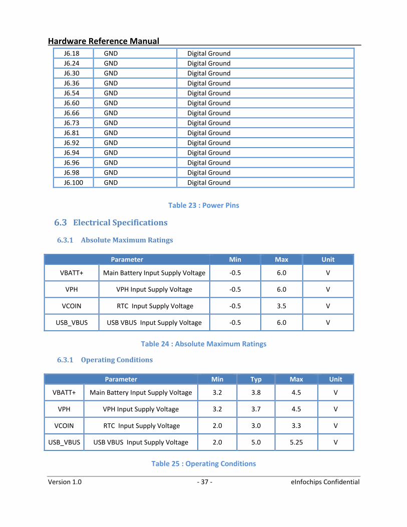
Hardware Reference Manual
Version 1.0 - 37 - eInfochips Confidential
J6.18 GND Digital Ground
J6.24 GND Digital Ground
J6.30 GND Digital Ground
J6.36 GND Digital Ground
J6.54 GND Digital Ground
J6.60 GND Digital Ground
J6.66 GND Digital Ground
J6.73 GND Digital Ground
J6.81 GND Digital Ground
J6.92 GND Digital Ground
J6.94 GND Digital Ground
J6.96 GND Digital Ground
J6.98 GND Digital Ground
J6.100 GND Digital Ground
Table 23 : Power Pins
Electrical Specifications
Absolute Maximum Ratings
Parameter Min Max Unit
VBATT+ Main Battery Input Supply Voltage -0.5 6.0 V
VPH VPH Input Supply Voltage -0.5 6.0 V
VCOIN RTC Input Supply Voltage -0.5 3.5 V
USB_VBUS USB VBUS Input Supply Voltage -0.5 6.0 V
Table 24 : Absolute Maximum Ratings
Operating Conditions
Parameter Min Typ Max Unit
VBATT+ Main Battery Input Supply Voltage 3.2 3.8 4.5 V
VPH VPH Input Supply Voltage 3.2 3.7 4.5 V
VCOIN RTC Input Supply Voltage 2.0 3.0 3.3 V
USB_VBUS USB VBUS Input Supply Voltage 2.0 5.0 5.25 V
Table 25 : Operating Conditions
Hardware Reference Manual
Version 1.0 - 38 - eInfochips Confidential
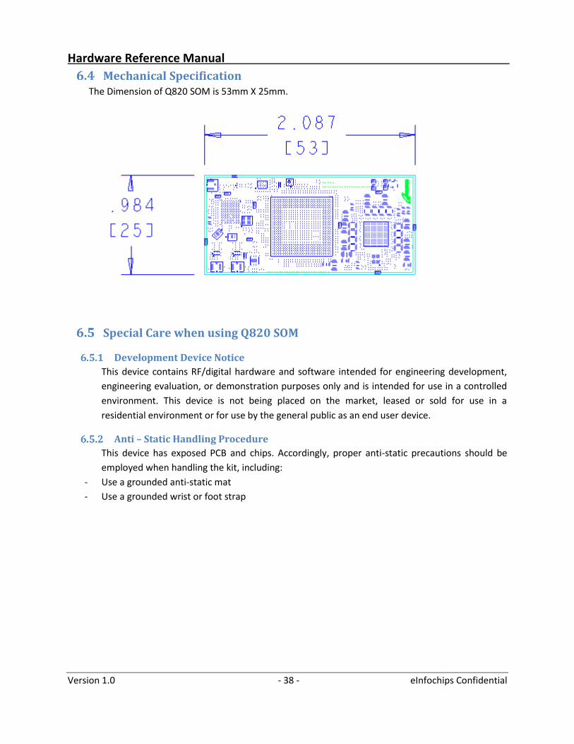
Mechanical Specification The Dimension of Q820 SOM is 53mm X 25mm.
Special Care when using Q820 SOM
Development Device Notice
This device contains RF/digital hardware and software intended for engineering development,
engineering evaluation, or demonstration purposes only and is intended for use in a controlled
environment. This device is not being placed on the market, leased or sold for use in a
residential environment or for use by the general public as an end user device.
Anti – Static Handling Procedure
This device has exposed PCB and chips. Accordingly, proper anti-static precautions should be
employed when handling the kit, including:
- Use a grounded anti-static mat
- Use a grounded wrist or foot strap

Hardware Reference Manual
Version 1.0 - 39 - eInfochips Confidential
7 About eInfochips
eInfochips is a partner of choice for Fortune 500 companies for product innovation and hi-tech engineering consulting. Since 1994, eInfochips has provided solutions to key verticals like Aerospace & Defense, Consumer Electronics, Energy & Utilities, Healthcare, Home, Office, and Industrial Automation, Media & Broadcast, Medical Devices, Retail & e-Commerce, Security & Surveillance, Semiconductor, Software/ISV and Storage & Compute.
Covering every aspect of the product lifecycle, eInfochips draws from an experience of building 500+ products that have over 10 Million units deployed – to provide solutions on Product Design and Development, QA and Certifications, Reengineering, Sustenance and Volume Production. Being an innovation driven company, 5% of our revenues are earmarked for building reusable IPs that will accelerate product design cycles and reduce product risks.
About 80% of eInfochips business comes from companies with revenues over $1 Billion, and 60% of total business from building life and mission critical products. eInfochips has the experience, expertise and infrastructure to deliver complex, critical and connected products.
Today, more than 1400 chip mates operate from over 10 Design Centers and dozen Sales Offices spread across Asia, Europe and US.
Our clients have recognized our teams for commitment, teamwork and initiatives that we have brought forward, adding immense value to client processes and products. Chip mates have a strong growth path defined for them, with specific soft-skills training modules – Lagaan, Pegasus and Altius – to groom leaders for the future.
‘At eInfochips we are determined that our growth should empower the ones in need. Every year we contribute 1% of our profits for development in education and healthcare’.
Contact Information:
Corporate Headquarter: USA Office:
eInfochips Ltd.
11 A/B Chandra Colony,
Behind Cargo Motors,
Off. C. G. Road,
Ellis bridge,
Ahmedabad 380 006
Tel +91-79-2656 3705
Fax +91-79-2656 0722
eInfochips, Inc.
1230 Midas Way, Suite# 200 Sunnyvale, CA 94085.
USA
Tel +1-408-496-1882
Fax +1-801-650-1480
Technical Assistance: eInfochips Qualcomm portal
(www.supportcenter.einfochips.com)
Technical Support: [email protected]
Sales/Marketing Support: [email protected]