hardware optimizations for crypto implementations...hardware optimizations for crypto...
TRANSCRIPT
HardwareOptimizations for
CryptoImplementations
TRS No. : XXXXX
Abstract:Latency, Area, and Power are three importantmetrics that a VLSI designer wants to optimize.However, often one of these may have to be op-timized at the cost of another or the other two.Depending on the application scenario, choice ofthe metric to optimize is made. In this paper,we consider hardware implementations of a num-ber of cryptographic primitives and present a num-ber of optimizations. We consider three areas ofcrypto-engineering. They are building physical un-clonable functions (PUFs), implementing encryp-tion/decryption algorithms, and side channel proofcrypto implementations. The techniques we employrange from area optimization through customizedmultiplexer design, fusing multiple operations intoa single hardware element, folding and unrollingof iterative algorithms, creating reconfigurable im-plementations to achieve multiple operations withthe same set of hardware elements, to techniques ofobfuscation to defeat fault injection based attackson the crypto implementation. All the proposedand existing designs are implemented with 45 nmCMOS library.
Mohamed Asan Basiri M andSandeep K Shukla, Department of
Computer Science and Engineering,Indian Institute of Technology
Kanpur, Utter Pradesh - 208016,India
1 Introduction
Cryptography is one of the necessities for cyber security. The crypto algorithms implemented insoftware have more flexibility than hardware but the performance and security in hardware aresuperior than software based designs. Performance of any hardware implementation is based on threefactors, namely (1) delay, (2) area, and (3) power dissipation. Certain functionalities such as physicalunclonable function (PUF) are always implemented in hardware, where the output depends on thephysical characteristics of the circuit such as path delay. However, in many applications, cryptoco-processors are used for accelerational crypto computation. Thus hardware implementations ofcrypto need to be optimized to reduce form factor (area and power consumption) or to improvelatency to have better performance. Unfortunately, various side channel attacks may exist if theimplementation is not carefully made side-channel attack resistant. For example, even scan chainand other testing harnesses in the hardware could lead to side channels. While studying variouscrypto implementations in hardware, we noticed scope for some interesting optimizations. However,each optimization is a trade-off between latency, power, and area (cost/form factor). The trade offdecisions are taken based on the application in which the implementation is used. So in this paper,we catalog some of these optimizations, and discuss some scenarios where custom implementationscould use our optimizations.
1.1 Related Works
PUFs are used to generate device specific unique signatures by exploiting the manufacturing char-acteristics. The ring oscillator (RO) PUF [1] falls under the category of delay based PUFs, whichis a reliable and light weight hardware. The oscillation frequency is varied due to its path delay.One of the advanced delay based PUF is proposed in [2], where series of non-inverting buffers areconnected along with registers. The output from these registers are fed into the multiplexers toobtain the final response. The main drawback with this approach is the requirement of high fan-inmultiplexers (MUXes). In the last decade, SRAM [3] played major role in PUF designs, where highfan-out row/column decoders are used to select one particular SRAM cell. The SRAM cell is madeup of two inverters. The drawback with this design is the requirement of larger decoders.
Elliptic curve cryptography (ECC) is one of the popular public key crypto algorithm, where thepoint addition and multiplication are the two important group operations. Kung Chi et. al [6] showsan efficient ECC hardware to perform point addition and multiplication in parallel. The group lawin ECC involves lots of multiplications followed by addition. So, there is a scope to fuse the additionalong with multiplication and this is the motivation of one of the proposed technique in this paper.Advance encryption standard (AES) is the most popular symmetric key crypto algorithm. AESwith 128-bits key length requires 10 rounds of operation. Each round includes 4 stages, namely (1)add key; (2) byte substitute; (3) shift row; and (4) mix column. The AES architecture with innerpipelined stages is shown in [7]. In case of folded architecture, the circuit for one round is iterativelyused to perform all the ten rounds. During a particular cycle, only one stage is busy out of four.The other three stages are idle but connected with common clock. This is the major drawback withpipelined folded AES [7]. S. S. Ali et. al [8] shows the AES architectures with different length ofdata path. In general, data path of AES architecture is 128-bits, which requires sixteen s-boxes andten rounds to complete one encryption. If the data path is 64-bits, then twenty cycles are requiredto perform one encryption.
In recent crypto engineering, fault tolerant designs [9] have become more important, wherethe crypto hardware designed in such a way so as to find the faults with corresponding necessaryactions. Involutional AES is explained in [10], where the encrypted output of each stage in a roundis decrypted immediately. Then the decrypted output is compared with original input of encryption.If both are not equal, then crypto hardware is injected with faults. To test the crypto hardware,scan chains [11] and built in self tests (BISTs) are used. The major advantage with scan chainand BIST are high fault coverage with less hardware cost and high hardware security respectively.The drawback with scan chain is less hardware security and with BIST is high hardware cost withless fault coverage. The work [12] suggests that apply the output from the crypto operation as
2
test vector. Usually, pseudo random number generators (PRNGs) are used to generate test vectorsin BIST based crypto systems. In stream ciphers [14], PRNG is used to generate the key valuefor encryption/decryption but the BIST feature is absent. This is the motivation of the proposedreconfigurable PRNG based stream ciphers, where the PRNG is used to generate test vectors duringtest mode.
In last two decades, reconfiguration is emerging trend in all the hardware implementations. Here,the same hardware is used to perform multiple functions or operations according to the requirement.AES and RSA algorithms are implemented on the same hardware in [16]. Weiwei et. al [17] showsthe reconfigurable implementation to perform AES or SMS4 on the single hardware. In the sameway, reconfigurable hardware for block cipher (SMS4) and hash function (Whirlpool) is proposed inthis paper.
1.2 Contribution of This Paper
This paper mainly focuses on (1) PUF, (2) ECC, (3) AES, (4) side channel resistant design, and (5)reconfigurable crypto hardware design. In PUF, larger multiplexer/decoders are the basic buildingblocks. If the size of multiplexer/decoder is increased, then the number of possible designs willbe exponential. Our proposed work brings the number of possible designs from exponential topolynomial and makes sure the best multiplexer/decoder design to be available in those polynomialset. Now, the larger multiplexer/decoder is designed by the tree of smaller components to reduce theworst case path delay or area. In case of ECC implementation, the multipliers followed by addersare replaced with proposed fused multiply add (FMA) designs, where the adder is combined withmodular multiplier. Hence, the worst case path delay of the circuit to compute group operations isreduced as compared with conventional design.
In the clock gating based pipelined AES, the inner stages of a round are isolated from clockif they are idle, which reduces the dynamic power. In the proposed reconfigurable vector AES,multiple encryptions are performed using the same circuit with trade-off in the number of cycles.In the proposed involutional AES, tri-state buffers are combined with scan chains to avoid testattacks. In the proposed stream cipher, reconfigurable PRNG is to generate keys and test vectorsin normal mode (encryption/decryption) and test mode respectively. Also, this paper proposes areconfigurable crypto hardware to perform multiple functions such as symmetric key encryption andhashing.
The rest of the paper is organized as follows: Section II describes the proposed hardware imple-mentations of various crypto primitives. Design modelling, implementation, and results are shownin Section III, followed by a conclusion in Section IV.
2 Proposed Hardware Implementations of Various CryptoPrimitives
2.1 High Performance Larger Multiplexer/Decoder based PUF Design
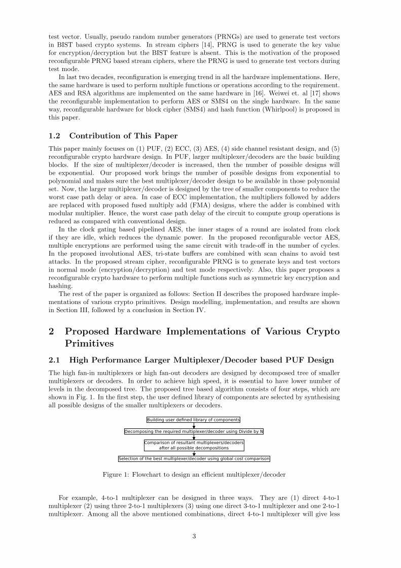
The high fan-in multiplexers or high fan-out decoders are designed by decomposed tree of smallermultiplexers or decoders. In order to achieve high speed, it is essential to have lower number oflevels in the decomposed tree. The proposed tree based algorithm consists of four steps, which areshown in Fig. 1. In the first step, the user defined library of components are selected by synthesisingall possible designs of the smaller multiplexers or decoders.
Figure 1: Flowchart to design an efficient multiplexer/decoder
For example, 4-to-1 multiplexer can be designed in three ways. They are (1) direct 4-to-1multiplexer (2) using three 2-to-1 multiplexers (3) using one direct 3-to-1 multiplexer and one 2-to-1multiplexer. Among all the above mentioned combinations, direct 4-to-1 multiplexer will give less
3
delay for a particular library, which has been used in this work. So, direct 4-to-1 multiplexer can beadded as a user defined library of components.
c
db2
db2 db2
db2
db2
db3
db3 db3 db3
db4
db4 db4
db4
db4
...............
.
.
.
a b c
N
d e f g h i j k l
Level 0
Level 1 after
split & merge
Level 2 after
split & merge
Figure 2: Decomposition procedure for N -to-1 multiplexer using the proposed algorithm
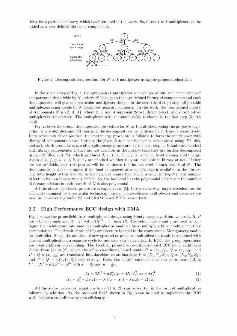
In the second step of Fig. 1, the given n-to-1 multiplexer is decomposed into smaller multiplexercomponents using divide by N , where N belongs to the user defined library of components and eachdecomposition will give one particular multiplexer design. In the next (third step) step, all possiblemultiplexers using divide by N decompositions are compared. In this work, the user defined libraryof components N ∈ {2, 3, 4}, where 2, 3, and 4 represent 2-to-1, direct 3-to-1, and direct 4-to-1multiplexers respectively. The multiplexer with minimum delay is chosen in the last step (fourthstep).
Fig. 2 shows the overall decomposition procedure for N -to-1 multiplexer using the proposed algo-rithm, where db2, db3, and db4 represent the decompositions using divide by 2, 3, and 4 respectively.Here, after each decomposition, the split/merge procedure is followed to form the multiplexer withlibrary of components alone. Initially the given N -to-1 multiplexer is decomposed using db2, db3,and db4, which produces a, b, c after split/merge procedure. In the next step, a, b, and c are checkedwith library components. If they are not available in the library, then they are further decomposedusing db2, db3, and db4, which produces d, e, f , g, h, i, j, k, and l in level 2 using split/merge.Again d, e, f , g, h, i, j, k, and l are checked whether they are available in library or not. If theyare not available, then this process will be continued till the last level of each branch of N . Thedecompositions will be stopped if the final component after split/merge is available in the library.The total height of this tree will be the height of binary tree, which is equal to (log2N). The numberof leaf nodes in a binary tree is 2height. So, the last level has the polynomial height and the numberof decompositions in each branch of N is also polynomial.
All the above mentioned procedure is explained in [5]. In the same way, larger decoders can beefficiently designed for a particular technology library. These efficient multiplexers and decoders areused in non-inverting buffer [2] and SRAM based PUFs respectively.
2.2 High Performance ECC design with FMA
Fig. 3 shows the prime field fused multiply add design using Montgomery algorithm, where A, B, Pare n-bit operands and R = 2n with RR−1 = 1 (mod P ). The select lines p and q are used to con-figure the architecture into modular multiplier or modular fused multiply add or modular multiplyaccumulation. The circuit depth of this architecture is equal to the conventional Montgomery modu-lar multiplier. Since, the addition of new operand or previous multiplication result is combined withcurrent multiplication, a separate cycle for addition can be avoided. In ECC, the group operationsare point addition and doubling. The Jacobian projective co-ordinate based ECC point addition isshown from (1) to (2), where the affine co-ordinate based points P = (x1, y1), Q = (x2, y2), andP + Q = (x3, y3) are translated into Jacobian co-ordinates as P = (X1, Y1, Z1), Q = (X2, Y2, Z2),and P + Q = (X3, Y3, Z3) respectively. Here, the elliptic curve in Jacobian co-ordinate [13] isY 2 = X3 + aXZ4 + bZ6 with x = X
Z2 and y = YZ3 .
λ1 = 3X21 + aZ4
1 ;λ2 = 4X1Y21 ;λ3 = 8Y 4
1 (1)
X3 = λ21 − 2λ2;Y3 = λ1(λ2 −X3)− λ3;Z3 = 2Y1Z1 (2)
All the above mentioned equations from (1) to (2) can be written in the form of multiplicationfollowed by addition. So, the proposed FMA shown in Fig. 3 can be used to implement the ECCwith Jacobian co-ordinate system efficiently.
4
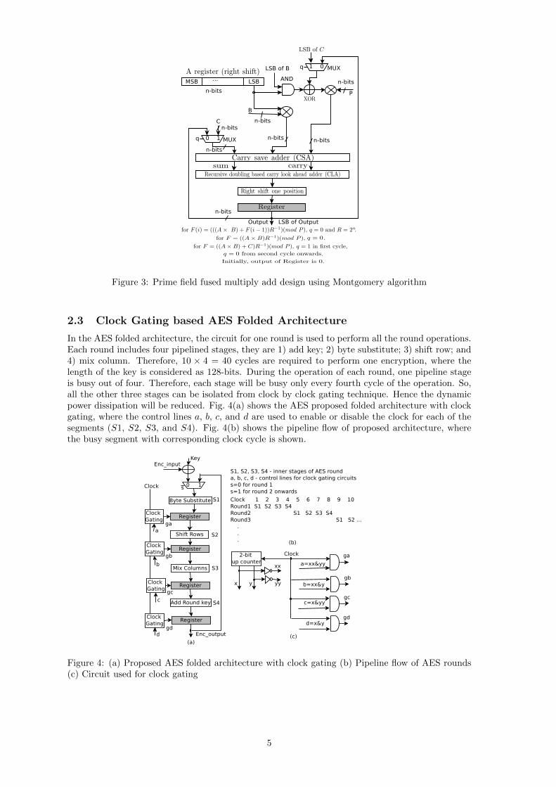
Figure 3: Prime field fused multiply add design using Montgomery algorithm
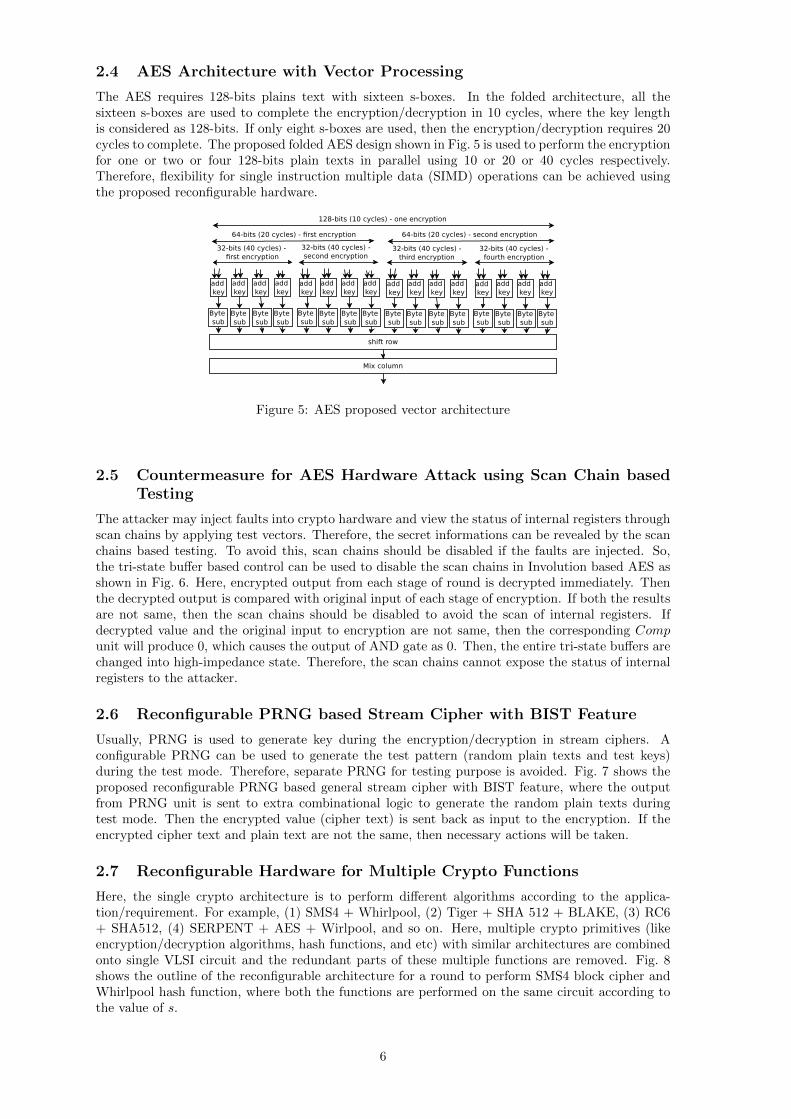
2.3 Clock Gating based AES Folded Architecture
In the AES folded architecture, the circuit for one round is used to perform all the round operations.Each round includes four pipelined stages, they are 1) add key; 2) byte substitute; 3) shift row; and4) mix column. Therefore, 10 × 4 = 40 cycles are required to perform one encryption, where thelength of the key is considered as 128-bits. During the operation of each round, one pipeline stageis busy out of four. Therefore, each stage will be busy only every fourth cycle of the operation. So,all the other three stages can be isolated from clock by clock gating technique. Hence the dynamicpower dissipation will be reduced. Fig. 4(a) shows the AES proposed folded architecture with clockgating, where the control lines a, b, c, and d are used to enable or disable the clock for each of thesegments (S1, S2, S3, and S4). Fig. 4(b) shows the pipeline flow of proposed architecture, wherethe busy segment with corresponding clock cycle is shown.
Figure 4: (a) Proposed AES folded architecture with clock gating (b) Pipeline flow of AES rounds(c) Circuit used for clock gating
5
2.4 AES Architecture with Vector Processing
The AES requires 128-bits plains text with sixteen s-boxes. In the folded architecture, all thesixteen s-boxes are used to complete the encryption/decryption in 10 cycles, where the key lengthis considered as 128-bits. If only eight s-boxes are used, then the encryption/decryption requires 20cycles to complete. The proposed folded AES design shown in Fig. 5 is used to perform the encryptionfor one or two or four 128-bits plain texts in parallel using 10 or 20 or 40 cycles respectively.Therefore, flexibility for single instruction multiple data (SIMD) operations can be achieved usingthe proposed reconfigurable hardware.
Figure 5: AES proposed vector architecture
2.5 Countermeasure for AES Hardware Attack using Scan Chain basedTesting
The attacker may inject faults into crypto hardware and view the status of internal registers throughscan chains by applying test vectors. Therefore, the secret informations can be revealed by the scanchains based testing. To avoid this, scan chains should be disabled if the faults are injected. So,the tri-state buffer based control can be used to disable the scan chains in Involution based AES asshown in Fig. 6. Here, encrypted output from each stage of round is decrypted immediately. Thenthe decrypted output is compared with original input of each stage of encryption. If both the resultsare not same, then the scan chains should be disabled to avoid the scan of internal registers. Ifdecrypted value and the original input to encryption are not same, then the corresponding Compunit will produce 0, which causes the output of AND gate as 0. Then, the entire tri-state buffers arechanged into high-impedance state. Therefore, the scan chains cannot expose the status of internalregisters to the attacker.
2.6 Reconfigurable PRNG based Stream Cipher with BIST Feature
Usually, PRNG is used to generate key during the encryption/decryption in stream ciphers. Aconfigurable PRNG can be used to generate the test pattern (random plain texts and test keys)during the test mode. Therefore, separate PRNG for testing purpose is avoided. Fig. 7 shows theproposed reconfigurable PRNG based general stream cipher with BIST feature, where the outputfrom PRNG unit is sent to extra combinational logic to generate the random plain texts duringtest mode. Then the encrypted value (cipher text) is sent back as input to the encryption. If theencrypted cipher text and plain text are not the same, then necessary actions will be taken.
2.7 Reconfigurable Hardware for Multiple Crypto Functions
Here, the single crypto architecture is to perform different algorithms according to the applica-tion/requirement. For example, (1) SMS4 + Whirlpool, (2) Tiger + SHA 512 + BLAKE, (3) RC6+ SHA512, (4) SERPENT + AES + Wirlpool, and so on. Here, multiple crypto primitives (likeencryption/decryption algorithms, hash functions, and etc) with similar architectures are combinedonto single VLSI circuit and the redundant parts of these multiple functions are removed. Fig. 8shows the outline of the reconfigurable architecture for a round to perform SMS4 block cipher andWhirlpool hash function, where both the functions are performed on the same circuit according tothe value of s.
6
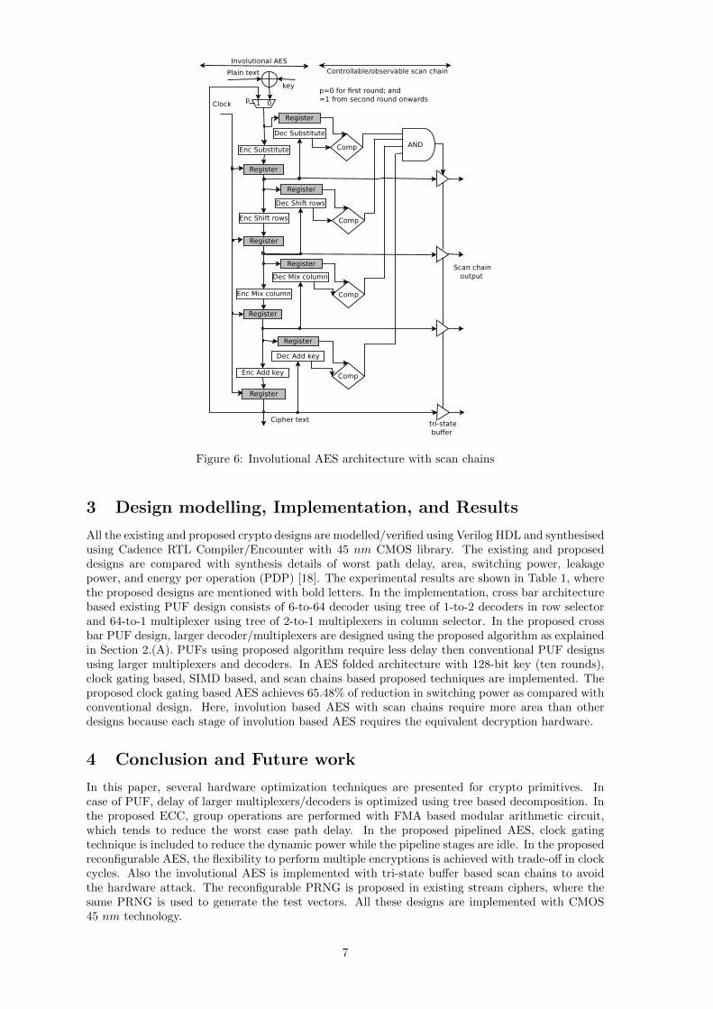
Figure 6: Involutional AES architecture with scan chains
3 Design modelling, Implementation, and Results
All the existing and proposed crypto designs are modelled/verified using Verilog HDL and synthesisedusing Cadence RTL Compiler/Encounter with 45 nm CMOS library. The existing and proposeddesigns are compared with synthesis details of worst path delay, area, switching power, leakagepower, and energy per operation (PDP) [18]. The experimental results are shown in Table 1, wherethe proposed designs are mentioned with bold letters. In the implementation, cross bar architecturebased existing PUF design consists of 6-to-64 decoder using tree of 1-to-2 decoders in row selectorand 64-to-1 multiplexer using tree of 2-to-1 multiplexers in column selector. In the proposed crossbar PUF design, larger decoder/multiplexers are designed using the proposed algorithm as explainedin Section 2.(A). PUFs using proposed algorithm require less delay then conventional PUF designsusing larger multiplexers and decoders. In AES folded architecture with 128-bit key (ten rounds),clock gating based, SIMD based, and scan chains based proposed techniques are implemented. Theproposed clock gating based AES achieves 65.48% of reduction in switching power as compared withconventional design. Here, involution based AES with scan chains require more area than otherdesigns because each stage of involution based AES requires the equivalent decryption hardware.
4 Conclusion and Future work
In this paper, several hardware optimization techniques are presented for crypto primitives. Incase of PUF, delay of larger multiplexers/decoders is optimized using tree based decomposition. Inthe proposed ECC, group operations are performed with FMA based modular arithmetic circuit,which tends to reduce the worst case path delay. In the proposed pipelined AES, clock gatingtechnique is included to reduce the dynamic power while the pipeline stages are idle. In the proposedreconfigurable AES, the flexibility to perform multiple encryptions is achieved with trade-off in clockcycles. Also the involutional AES is implemented with tri-state buffer based scan chains to avoidthe hardware attack. The reconfigurable PRNG is proposed in existing stream ciphers, where thesame PRNG is used to generate the test vectors. All these designs are implemented with CMOS45 nm technology.
7
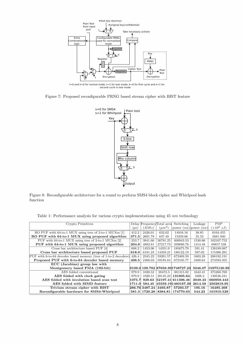
Figure 7: Proposed reconfigurable PRNG based stream cipher with BIST feature
Figure 8: Reconfigurable architecture for a round to perform SMS4 block cipher and Whirlpool hashfunction
Table 1: Performance analysis for various crypto implementations using 45 nm technology
Crypto Primitives Delay FrequencyTotal area Switching Leakage PDP(ps) (MHz) (µm2) power (nw) power (nw) (×103 zJ)
RO PUF with 64-to-1 MUX using tree of 2-to-1 MUXes [1] 412.2 2426.01 632.02 14916.16 38.85 6164.455RO PUF with 64-to-1 MUX using proposed algorithm 371.5 2691.79 637.49 15259.06 35.53 5681.940
PUF with 64-to-1 MUX using tree of 2-to-1 MUXes [2] 253.7 3941.66 26791.25 400943.53 1530.86 102107.752PUF with 64-to-1 MUX using proposed algorithm 204.8 4882.81 27217.73 339686.78 1414.48 69857.538
Cross bar architecture based PUF [4] 688.2 1453.06 14351.0 185675.79 591.41 128189.087Cross bar architecture based proposed PUF 618.0 6181.23 14359.21 186122.19 587.02 115386.291
PUF with 6-to-64 decoder based memory (tree of 1-to-2 decoders) 426.4 2345.22 59201.57 672469.59 3403.28 288192.191Proposed PUF with 6-to-64 decoder based memory 406.5 2460.03 59185.84 672105.77 3400.64 274593.355
ECC (Jacobian) group law withMontgomery based FMA (192-bit) 9109.0 109.782 87659.391748727.23 5046.07 15975120.99
AES folded conventional 979.9 1020.52 28472.5 381315.82 1642.41 375260.769AES folded with clock gating 979.9 1020.51 28145.23 131605.64 1608.2 130536.241
AES folded with involution based scan test 1075.7 929.63 52197.41 611396.46 3049.43 660959.443AES folded with SIMD feature 1711.0 584.45 45559.191460167.39 2614.58 2502819.95
Trivium stream cipher with BIST 286.76 3487.24 3493.87 57293.57 195.16 16485.468Reconfigurable hardware for SMS4-Whirlpool 581.3 1720.28 8384.81 174770.63 544.23 101910.528
8
The future work is to reduce the total number of CMOS transistors (by exploiting user definedlibrary of CMOS transistor based components) in critical path of SRAM based PUF to optimizedelay.
References
[1] C. E. Yin and Gang Qu, “LISA: Maximizing RO PUF’s Secret Extraction”, IEEE InternationalSymposium on Hardware-Oriented Security and Trust (HOST), pp. 100-105, June 2010.
[2] Aydin Aysu, Patrick Schaumont, “Hardware/software Co-design of Physical Unclonable Func-tion based Authentications on FPGAs”, Journal of Microprocessors and Microsystems, Elsevier,vol. 39, no. 7, pp. 589-597, Oct. 2015.
[3] Yu Zheng, Maryam S. Hashemian, and Swarup Bhunia, “RESP: A Robust Physical UnclonableFunction Retrofitted into Embedded SRAM Array”, 50th ACM/EDAC/IEEE Design Automa-tion Conference (DAC), pp. 1-9, June 2013.
[4] Pai-Yu Chen, Runchen Fang, Rui Liu, Chaitali Chakrabarti, and Yu Cao; Shimeng Yu, “Ex-ploiting resistive corss-point array for compact design of physical unclonable function”, IEEEInternational Symposium on Hardware Oriented Security and Trust (HOST), pp. 26-31, May2015.
[5] Mohamed Asan Basiri M and Noor Mahammad Sk, “High Speed Multiplexer Design Using TreeBased Decomposition Algorithm”, Microelectronics Journal, Elesevier, vol. 51, pp. 99-111, May2016.
[6] Kung Chi Cinnati Loi and Seok-Bum Ko, “Scalable Elliptic Curve Cryptosystem FPGA Pro-cessor for NIST Prime Curves”, IEEE Transactions on Very Large Scale Integration (VLSI)Systems, vol. 23, no. 11, pp. 2753-2756, Nov. 2015.
[7] Jose M. Granado-Criado, Miguel A. Vega-Rodrguez, Juan M. Sanchez-Perez, and Juan A. Gomez-Pulido, “A New Methodology to Implement the AES Algorithm using Partial and DynamicReconfiguration”, Integration the VLSI Journal, Elsevier, vol. 43, pp. 72-80, Jan. 2010.
[8] S. S. Ali, O. Sinanoglu, and R. Karri, “AES Design Space Exploration New Line for Scan AttackResiliency”, 22nd IEEE International Conference on Very Large Scale Integration (VLSI-SoC),pp. 1-6, Oct. 2014.
[9] Akashi Satoh, Takeshi Sugawara, NaofumiHomma, and TakafumiAoki, “High-performance Con-current Error Detection Scheme for AES Hardware”, Cryptographic Hardware and EmbeddedSystems-CHES, Springer Berlin Heidelberg, pp. 100-112, Aug. 2008.
[10] Nikhil Joshi, KaijieWu, Jayachandran Sundararajan, and Ramesh Karri, “Concurrent Error De-tection for Involutional Functions with Applications in Fault-Tolerant Cryptographic HardwareDesign”, IEEE Transactions on Computer Aided Design of Integrated Circuts and Systems,vol. 25, no. 6, pp. 1163-1169, June 2007.
[11] Gaurav Sengar, Debdeep Mukhopadhayay, and D. Roy Chowdhury, “An Efficient Approachto Develop Secure Scan Tree for Crypto- Hardware”, 15th IEEE International Conference onAdvanced Computing and Communications, pp. 21-26, Dec. 2007.
[12] D. Karaklajic, M. Knezevic, and I. Verbauwhede, “Low Cost Self Test of Crypto Devices”,IEEE Workshop on Fault Diagnosis and Tolerance in Cryptography (FDTC), pp. 97-103, Aug.2010.
[13] T. Abdurahmonov, Eng-Thiam Yeoh, and Helmi Mohamed Hussain, “A Proposed Implemen-tation of Elliptic Curve Exponentiation over Prime Field (Fp) in the Global Smart Cards”,International Journal of Information and Electronics Engineering, vol. 3, no. 1, pp. 72-76, Jan.2013
[14] Paris Kitsos, Nicolas Sklavos, George Provelengios, and Athanassios N. Skodras, “FPGA-basedPerformance Analysis of Stream Ciphers ZUC, Snow3g, Grain V1, Mickey V2, Trivium andE0 ”, Journal of Microprocessors and Microsystems, Elsevier, vol. 37, pp. 235-245, 2013.
9
[15] M. D. Galanis, P. Kitsos, G. Kostopoulos, N. Sklavos, O. Koufopavlou, and C.E. Goutis, “Com-parison of the Hardware Architectures and FPGA Implementations of Stream Ciphers”, 11th
IEEE International Conference on Electronics, Circuits and Systems, pp. 571-574, Dec. 2004.
[16] A. Nadjia and A. Mohamed, “AES IP for Hybrid Cryptosystem RSA-AES”, 12th IEEE Inter-national Multi-Conference on Systems, Signals & Devices (SSD), pp. 1-6, Mar. 2015.
[17] Weiwei Yan, Kaidi You, Jun Han, and Xiaoyang Zeng, “A Low Cost Reconfigurable VLSIImplementation of the SMS4 and AES Algorithm”, 8th IEEE International Conference on ASIC,pp. 135-138, Oct. 2009.
[18] Ricardo Gonzalez, Benjamin M. Gordon, and Mark A. Horowitz, “Supply and Threshold VoltageScaling for Low Power CMOS”, IEEE Journal of Solid State Circuits, vol. 32, no. 8, pp. 1210-1216, Aug. 1997.
10