hardware architecture of 68000 - ump...
TRANSCRIPT

Chapter 9
Hardware Architecture of 68000
Expected OutcomesDescribe the internal architecture of 68000Describe general specification of 68000 microprocessorOutline the processor’s control signals name and functionsSketch the general timing signal for read and write operation
NMKNYFKEEUMP

68xxx Family
Product Numbering System for the 68xxx Family (Motorola Product)
MC 68HC X C FG 16 V B
Status Product
MC - Fully qualified
XC - Partial Qualified
PC - Product Engineering
Part/Module Modifier
EC - Embedded Controller
LC - Low cost, no FPU
BLANK - Full CPU
HC - HCMOS
SEC - Static Embedded Product Designator
000,010,020 etc
Temperature Range
BLANK = 0 - 70oC
B = -40 - 70oC
C = -40 - 85oC
Packaging Designator
Speed
Voltage
BLANK = 5V
V = 3.3V
Die Mask Revision
NMKNYFKEEUMP

Pin Configuration
NMKNYFKEEUMP

68000 Manufacturer
Manufacturer Description
Apple 68000-8 8 MHz, 64-pin side-brazed ceramic DIP
Hitachi HD68000-8 8 MHz, 64-pin side-brazed ceramic DIP
Mostek MK68000-8B 8 MHz, 64-pin plastic DIP
Motorola XC68000L 64-pin side-brazed ceramic DIP
Rockwell R68000C8 8 MHz, 64-pin side-brazed ceramic DIP
SGS-Thompson TS68000CP10 10 MHz, 64-pin plastic DIP
Signetics SCN68000C4164 4 MHz, 64-pin side-brazed ceramic DIP
Thompson TS68000CFN16 16 MHz, 68 Lead plastic LCC
Toshiba TMP68HC000P-10 10MHz, 64-pin plastic DIP
Motorola MC68HC000LC8 8 MHz, 64-pin side-brazed ceramic DIP
Hitachi HD68000Y10 10 MHz, 68-pin ceramic PGA
NMKNYFKEEUMP

68000
NMKNYFKEEUMP

Timing Diagram
Instruction cycle
A complete cycle for 68000 to read and execute an instruction
Bus cycle
Time for 68000 to read or write a byte/word from memory
Clock cycle (cc)
Time between two consecutive positive edge and equal to clock duration and require 4 cc in each bas cycle
S0 S1 S2 S3 S4 S5 S6 S7 S0 S1 S2
Clock cycle
bus cycle
NMKNYFKEEUMP

68000 Pin Function
MC68000
VCC (2)GND (2)
CLK
IPL0*IPL1*IPL2*
EVMA*VPA*
BERR*RESET*
HALT*
BR*BG*
BGACK*
ADDRESS
DATA
A1-A23
D0-D15
AS*R/W*UDS*LDS*DTACK*
FC0FC1FC2
NMKNYFKEEUMP
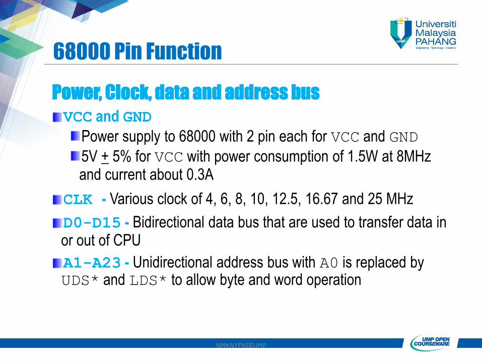
68000 Pin Function
Power, Clock, data and address bus
VCC and GND
Power supply to 68000 with 2 pin each for VCC and GND
5V + 5% for VCC with power consumption of 1.5W at 8MHz and current about 0.3A
CLK - Various clock of 4, 6, 8, 10, 12.5, 16.67 and 25 MHz
D0-D15 - Bidirectional data bus that are used to transfer data in or out of CPU
A1-A23 - Unidirectional address bus with A0 is replaced by UDS* and LDS* to allow byte and word operation
NMKNYFKEEUMP

68000 Pin Function
Asynchronous Signal for Hardware Operation
AS* (Address Strobe) - output
When AS* goes low, A1-A23 are valid address
R/W* (Read/Write) - output
Determine read (high) or write (low) operation
UDS* (Upper Data Strobe) - output
Control the transfer of upper data bus (D8-D15)
LDS* (Lower Data Strobe) - output
Control the transfer of upper data bus (D0-D7)
NMKNYFKEEUMP

68000 Pin Function
DTACK* (Data Transfer Acknowledge) - input
When CPU receives a low signal, it assumes this is the end of bus cycle
I/O device must activate the DTACK pin correctly
Signal Function (when asserted)
AS Output signal indicating valid memory address available on
address bus
R/W Output signal indicating read cycle when HIGH and write
cycle when LOW
UDS Together with LDS signal, output an encoded signal based
on internal state of A0 address line
LDS Together with UDS signal, output an encoded signal based
on internal state of A0 address line
DTACK Input signal indicating data transfer during read/write
cycle is completed
NMKNYFKEEUMP

Memory Map
Due to the data bus size of 16-bit, memory map is consisted of two byte
UDS* and LDS* are used to access even and odd location respectively
To access a byte of odd address, UDS*=1, LDS*=0
To access a byte of even address, UDS*=0, LDS*=1
To access a word, UDS*=0, LDS*=0
$000000
$000002
$000004
$000006
$FFFFF8
$FFFFFA
$FFFFFC
$FFFFFE
15 08 7
even address odd address
LDS*UDS*
NMKNYFKEEUMP

Byte Addressing
MC68000
ODD MEMORY
EVEN MEMORY
A1 - A23
D0-D15
R/W*
LDS*
D0 - D7
D8 - D15
UDS*
UDS* LDS* R/W*
1 1 -
0 0 1
1 0 1
0 1 1
0 0 0
1 0 0
0 1 0
D8 - D15 D0 - D7
Illegal data Illegal data
Bit 8 - 15 Bit 0 - 7
lllegal data Bit 0 -7
Bit 8 - 15 lllegal data
Bit 8 - 15 Bit 0 - 7
Illegal data Bit 0 - 7
Bit 8 - 15 Illegal data
16-bit read
8-bit read
16-bit write
8-bit write
NMKNYFKEEUMP
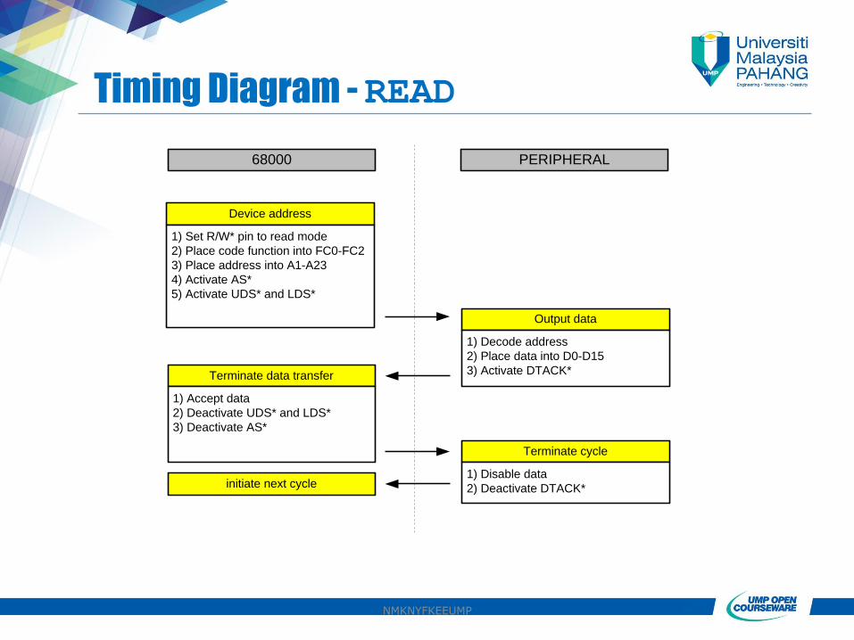
Timing Diagram -READ
Device address
1) Set R/W* pin to read mode
2) Place code function into FC0-FC2
3) Place address into A1-A23
4) Activate AS*
5) Activate UDS* and LDS*
Output data
1) Decode address
2) Place data into D0-D15
3) Activate DTACK*Terminate data transfer
1) Accept data
2) Deactivate UDS* and LDS*
3) Deactivate AS*
Terminate cycle
1) Disable data
2) Deactivate DTACK*initiate next cycle
68000 PERIPHERAL
NMKNYFKEEUMP

Timing Diagram -READ
S0 S1 S2 S3 S4 S5 S6 S7 S0
CLK
A1 - A23
R/W*
AS*
UDS*, LDS*
DTACK*
D0- D15 valid data
valid
address
NMKNYFKEEUMP
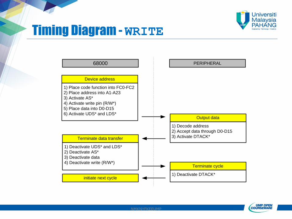
Timing Diagram -WRITE
Device address
1) Place code function into FC0-FC2
2) Place address into A1-A23
3) Activate AS*
4) Activate write pin (R/W*)
5) Place data into D0-D15
6) Activate UDS* and LDS*Output data
1) Decode address
2) Accept data through D0-D15
3) Activate DTACK*Terminate data transfer
1) Deactivate UDS* and LDS*
2) Deactivate AS*
3) Deactivate data
4) Deactivate write (R/W*)Terminate cycle
1) Deactivate DTACK*initiate next cycle
68000 PERIPHERAL
NMKNYFKEEUMP

Timing Diagram -WRITES0 S1 S2 S3 S4 S5 S6 S7 S0
CLK
A1 - A23
R/W*
AS*
UDS*, LDS*
DTACK*
D0- D15 valid data
valid address
NMKNYFKEEUMP
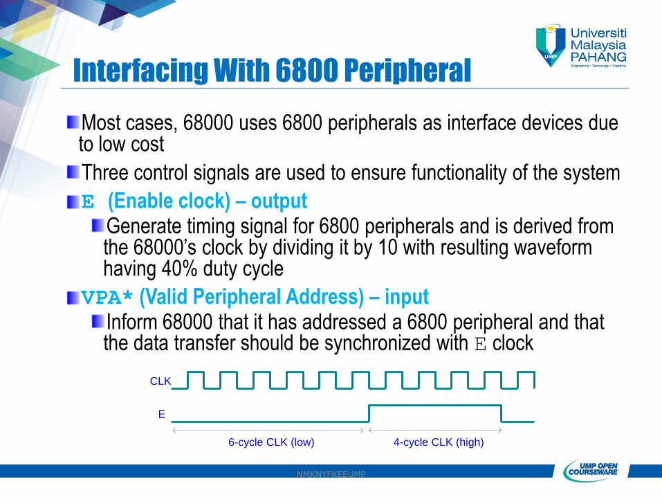
Interfacing With 6800 Peripheral
Most cases, 68000 uses 6800 peripherals as interface devices due to low cost
Three control signals are used to ensure functionality of the system
E (Enable clock) – outputGenerate timing signal for 6800 peripherals and is derived from the 68000’s clock by dividing it by 10 with resulting waveform having 40% duty cycle
VPA* (Valid Peripheral Address) – inputInform 68000 that it has addressed a 6800 peripheral and that the data transfer should be synchronized with E clock
CLK
E
6-cycle CLK (low) 4-cycle CLK (high)
NMKNYFKEEUMP

Interfacing With 6800 Peripheral
VMA* (Valid Memory Address) – output
Goes low when the processor synchronizes with E clock allowing data transfer
Signal Function (when asserted)
E Output a synchronous timing (clock) for proper
information transfer between the microprocessor and the
M6800 peripheral devices
VPA inform the microprocessor that an M6800 peripheral
device has been addressed and data transfer to be
synchronized with E clock
VMA inform M6800 peripheral device that it has been
addressed by the address bus and data transfer is
synchronized to E clock
NMKNYFKEEUMP

Interfacing With 6800 Peripheral
Interface with peripheral devices involves E, VMA* and VPA pins to ensure proper functionality of the system as 6800 devices operate in synchronous mode
68000 6800 device
Address
decoder
address bus
AS
*
VPA
*
VMA*
E
CS*
CS*
E
R/
W*R/
W*
NMKNYFKEEUMP

Interfacing With 6800 Peripheral
Initiate cycle
1) CPU initiates read or write cycleDefine 6800 cycle
1) External hardware activate VPA*
Synchronize with E clock
1) CPU waits until E goes low
2) CPU activate VMA*Data Transfer
1) Peripheral waits until E is active
before transferring data
initiate next cycle
68000 PERIPHERAL
Terminate cycle
1) CPU waits until E goes low
2) CPU disables VMA*
3) CPU disable AS*, UDS* and LDS*
NMKNYFKEEUMP
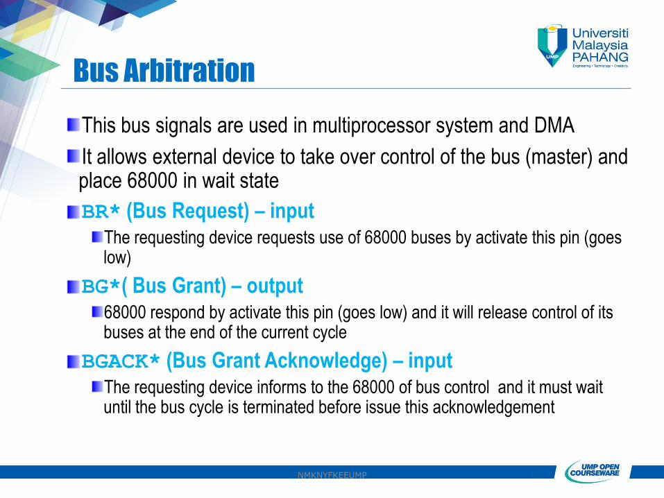
Bus Arbitration
This bus signals are used in multiprocessor system and DMA
It allows external device to take over control of the bus (master) and place 68000 in wait state
BR* (Bus Request) – inputThe requesting device requests use of 68000 buses by activate this pin (goes low)
BG*( Bus Grant) – output68000 respond by activate this pin (goes low) and it will release control of its buses at the end of the current cycle
BGACK* (Bus Grant Acknowledge) – inputThe requesting device informs to the 68000 of bus control and it must wait until the bus cycle is terminated before issue this acknowledgement
NMKNYFKEEUMP

Bus Arbitration
MC68000Master
bus 1
Master
bus 2
Master
bus 3
Address buses
BGACK*
BR*
BG*
+5V +5V
This arbitration signals are required to allow more than one processor to control buses
NMKNYFKEEUMP

Exception Processing68000 microprocessor operates in two modes; user execution mode and
supervisor execution mode
In user execution mode, the microprocessor operates in normal processing
environment suitable for user’s application programs
Supervisor mode provides programmers with full access to the
microprocessor’s instructions and status register
The mode is determined by the thirteenth bit (S-bit) in the status register. Setting
the S-bit in the status register puts the microprocessor in the supervisor mode
Exception is one of the three processing states of a microprocessor. This is the
processing state where microprocessor handles all internally or externally
generated exceptions
Examples of exception are external hardware interrupts, external hardware
RESET, internal RESET/TRAP instructions, tracing, bus error and execution
errors
NMKNYFKEEUMP
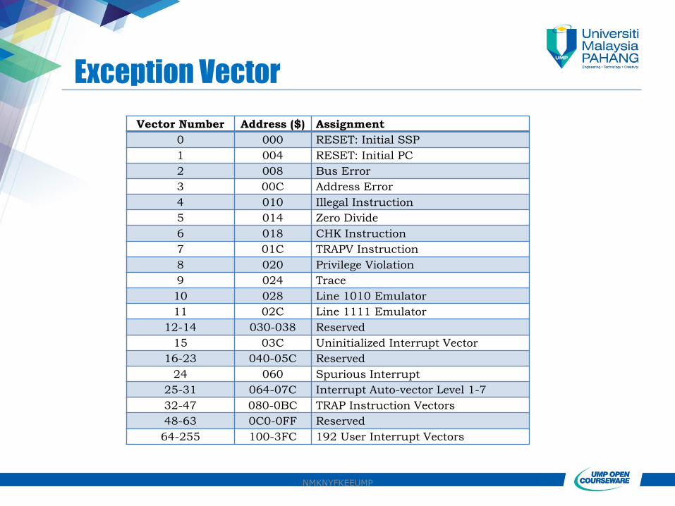
Exception Vector
Vector Number Address ($) Assignment
0 000 RESET: Initial SSP
1 004 RESET: Initial PC
2 008 Bus Error
3 00C Address Error
4 010 Illegal Instruction
5 014 Zero Divide
6 018 CHK Instruction
7 01C TRAPV Instruction
8 020 Privilege Violation
9 024 Trace
10 028 Line 1010 Emulator
11 02C Line 1111 Emulator
12-14 030-038 Reserved
15 03C Uninitialized Interrupt Vector
16-23 040-05C Reserved
24 060 Spurious Interrupt
25-31 064-07C Interrupt Auto-vector Level 1-7
32-47 080-0BC TRAP Instruction Vectors
48-63 0C0-0FF Reserved
64-255 100-3FC 192 User Interrupt Vectors
NMKNYFKEEUMP
Self-Test
Exercise
Explain the difference between synchronous and asynchronous data bus transfer and explain the bus signals used in each method
Exercise
State the number of data and address bus for 68000. Explain why the A0 pin is not part of 68000
Exercise
State the logic of UDS*,LDS*,AS*,A13 and R/W* when
(i) a byte write to address $4000
(ii) a byte read from address $5678
(iii) a word write to address $6542
NMKNYFKEEUMP
Self-Test
Exercise
Explain the importance of DTACK pin in asynchronous data bus transfer
Exercise
Briefly explain the use of wait states in memory access
Exercise
State the bus direction for each pin
(i) DTACK* (ii) D8 (iii) A6 (iv) R/W*
(v) BGACK* (vi) VPA* (vii) E (viii) UDS*
NMKNYFKEEUMP