handouts stanford
TRANSCRIPT
STANFORD UNIVERSITY Department of Electrical Engineering
Prof. Boris Murmann
EE214: Analog Integrated Circuit Design - Autumn 2007/08 -
http://eeclass.stanford.edu/ee214/
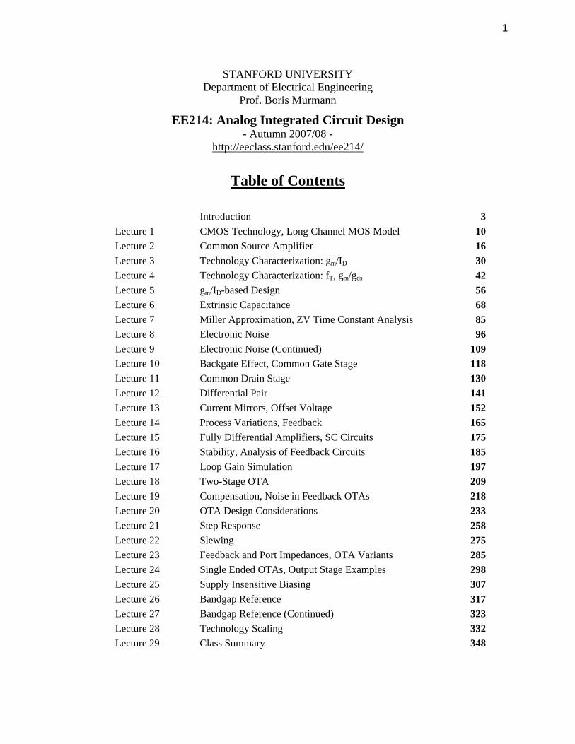
Table of Contents
Introduction 3
Lecture 1 CMOS Technology, Long Channel MOS Model 10
Lecture 2 Common Source Amplifier 16
Lecture 3 Technology Characterization: gm/ID 30
Lecture 4 Technology Characterization: fT, gm/gds 42
Lecture 5 gm/ID-based Design 56
Lecture 6 Extrinsic Capacitance 68
Lecture 7 Miller Approximation, ZV Time Constant Analysis 85
Lecture 8 Electronic Noise 96
Lecture 9 Electronic Noise (Continued) 109
Lecture 10 Backgate Effect, Common Gate Stage 118
Lecture 11 Common Drain Stage 130
Lecture 12 Differential Pair 141
Lecture 13 Current Mirrors, Offset Voltage 152
Lecture 14 Process Variations, Feedback 165
Lecture 15 Fully Differential Amplifiers, SC Circuits 175
Lecture 16 Stability, Analysis of Feedback Circuits 185
Lecture 17 Loop Gain Simulation 197
Lecture 18 Two-Stage OTA 209
Lecture 19 Compensation, Noise in Feedback OTAs 218
Lecture 20 OTA Design Considerations 233
Lecture 21 Step Response 258
Lecture 22 Slewing 275
Lecture 23 Feedback and Port Impedances, OTA Variants 285
Lecture 24 Single Ended OTAs, Output Stage Examples 298
Lecture 25 Supply Insensitive Biasing 307
Lecture 26 Bandgap Reference 317
Lecture 27 Bandgap Reference (Continued) 323
Lecture 28 Technology Scaling 332
Lecture 29 Class Summary 348
1

2

EE 214 IntroductionB. Murmann 1
EE214Analog Integrated Circuit Design
Boris MurmannStanford University
Copyright © 2007 by Boris Murmann
EE 214 IntroductionB. Murmann 2
A Few Words About Your Instructor
• Assistant Professor in EE since 2004
• PhD, UC Berkeley 2003
– Digitally assisted A/D conversion
– Use "minimalistic" analog circuits (low power, fast)
– Correct errors using digital post-processor
• ~ 4 years work experience in IC industry
– Mixed signal IC design, low power, high voltage
• Current research
– Digital correction techniques for data converters
– Sensor interfaces
– Circuit design in new technologies• Post-CMOS devices, organic devices
3

EE 214 IntroductionB. Murmann 3
EE214 Basics (1)
• Teaching assistants
– Mohammad Hekmat, Bob Wiser, Ross Walker
• Administrative support
– Ann Guerra, CIS 207
• Lectures are televised
– But please come to class to keep the discussion interactive!
• Web page: http://eeclass.stanford.edu/ee214
– Check regularly, especially bulletin board
– Register for online access to grades and solutions• Only enrolled students can register; we manually control the
access list based on Axess data
EE 214 IntroductionB. Murmann 4
EE214 Basics (2)
• Required text
– Analysis and Design of Analog Integrated Circuits, 4th
Edition, Gray, Hurst, Lewis and Meyer, Wiley, 2001. (On reserve in Engineering Library)
• Course prerequisites
– EE101B or equivalent
– Basic device physics and models• PN junctions, MOSFETs, BJTs
– Basic linear systems• Frequency response, poles, zeros
– Some exposure to a circuit simulator, basic Unix commands
– May consider concurrent enrollment in EE114X to brush up on the above (primarily for undergraduates)
4

EE 214 IntroductionB. Murmann 5
Assignments
• Homework (20%)– Handed out on Mondays, due following Monday in class– Late policy
• Score drops 0.5 dB per hour after deadline
– Lowest HW score will be dropped– Policy for off-campus students: Fax/email to SCPD before
deadline stated on handout
• Midterm Exam (30%)
• Project (20%)– Design of an amplifier using HSpice (no layout)– Work in teams of two
• OK to discuss with other teams, but no file exchange!
• Final Exam (30%)
EE 214 IntroductionB. Murmann 6
Honor Code
• Please remember you are bound by the honor code
– I will trust you not to cheat
– I will try not to tempt you
• But if you are found cheating it is very serious
– There is a formal hearing
– You can be thrown out of Stanford
• Save yourself and me a huge hassle and be honest
• For more info
– http://www.stanford.edu/dept/vpsa/judicialaffairs/guiding/pdf/honorcode.pdf
5
EE 214 IntroductionB. Murmann 7
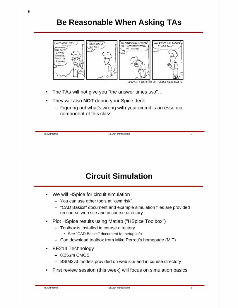
Be Reasonable When Asking TAs
• The TAs will not give you "the answer times two"…
• They will also NOT debug your Spice deck
– Figuring out what's wrong with your circuit is an essential component of this class
EE 214 IntroductionB. Murmann 8
Circuit Simulation
• We will HSpice for circuit simulation– You can use other tools at "own risk"
– "CAD Basics" document and example simulation files are provided on course web site and in course directory
• Plot HSpice results using Matlab ("HSpice Toolbox")– Toolbox is installed in course directory
• See "CAD Basics" document for setup info
– Can download toolbox from Mike Perrott's homepage (MIT)
• EE214 Technology– 0.35μm CMOS
– BSIM3v3 models provided on web site and in course directory
• First review session (this week) will focus on simulation basics
6

EE 214 IntroductionB. Murmann 9
The Spice Monkey Problem (1)
• What most people know
– Even a very large number of monkeys randomly arranging characters will never manage to write an interesting book
• What some people tend to forget
– Even a very large number of "Spice Monkeys" randomly tweaking circuits will never manage to design a robust, optimized IC
[Courtesy Isaac Martinez]
EE 214 IntroductionB. Murmann 10
The Spice Monkey Problem (2)
• Simply put
– Spice is nothing but a "calculator" that lets you evaluate and test your ideas
– There is no need to simulate anything unless you already know the (approximate) answer!
– Must always be aware of modeling limitations
• Especially in the integrated circuits arena, uneducated, purely simulator driven design can be costly
– Mask sets cost up to $2 Million (90 nm production)
– Turnaround time is on the order of months
– If your chip doesn't work, you cannot simply send the customer a "patch"…
7

EE 214 IntroductionB. Murmann 11
Analysis versus Design
• Unlike common perception, analog circuit analysis and design is not "black magic"
• Circuit analysis– The art of decomposing a circuit into manageable pieces– Based on the simple, but sufficiently accurate model
• "Just-in-time" modeling; do not use a complex model unless you know why it's needed…
– One circuit ⇒ one solution
• Circuit design– The art of synthesizing circuits based on experience from
extensive analysis– One set of specifications ⇒ Many solutions– Design skills are best acquired through "learning by doing"
• This is why we'll have a design project…
EE 214 IntroductionB. Murmann 12
Learning Goals
• Develop deeper understanding of MOS device behavior relevant to analog design
• Develop a feel for limits and tradeoffs in analog circuits (speed, noise, power dissipation)
• Learn to bridge the gap between complex device models/behavior and basic hand calculations
– Design using look-up tables, "gm/ID methodology"
• Develop a systematic, non-spice-monkey design style
• Solidify the above aspects in a hands-on design project
– Design and optimization of a high performance feedback amplifier used in many industrial circuits/applications
8
EE 214 IntroductionB. Murmann 13
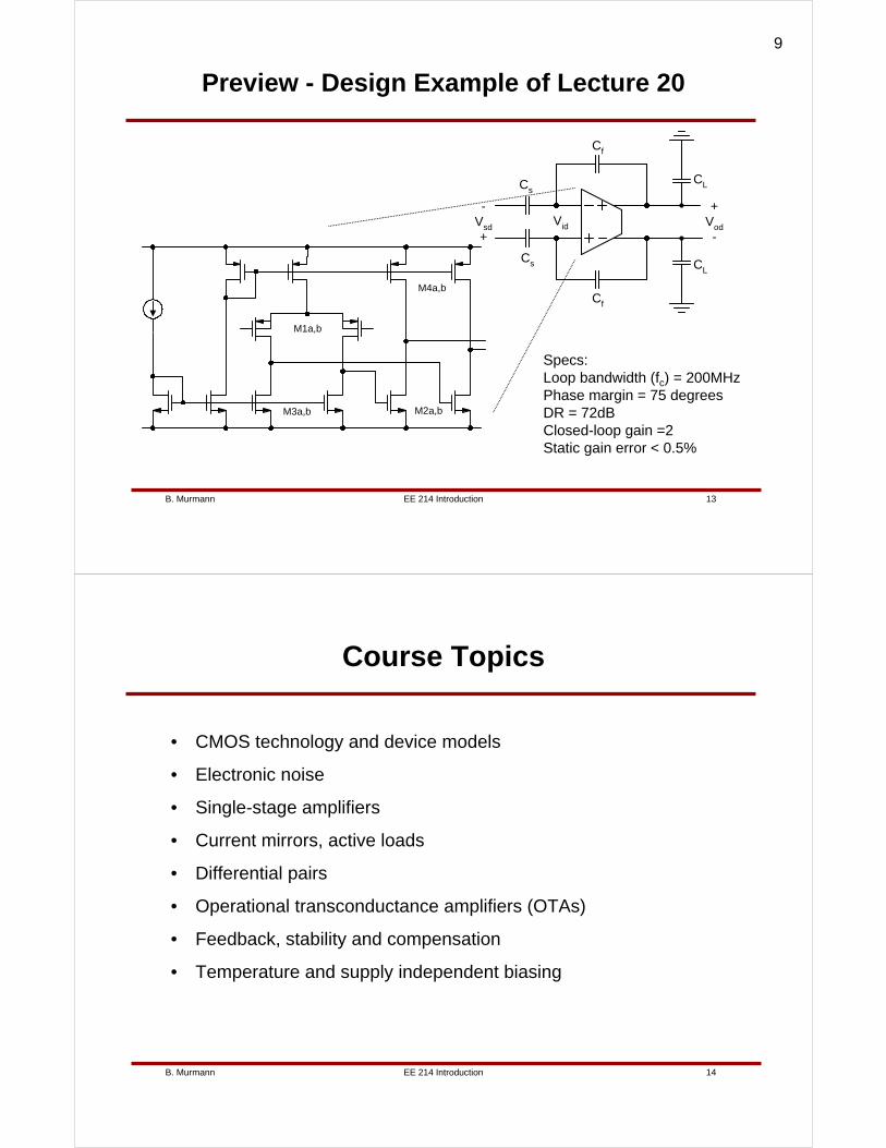
Preview - Design Example of Lecture 20
Cs
-Vsd+
+Vod-
Cs
Cf
Cf
CL
CL
Vid
M1a,b
M2a,bM3a,b
M4a,b
Specs:Loop bandwidth (fc) = 200MHzPhase margin = 75 degreesDR = 72dBClosed-loop gain =2Static gain error < 0.5%
EE 214 IntroductionB. Murmann 14
Course Topics
• CMOS technology and device models
• Electronic noise
• Single-stage amplifiers
• Current mirrors, active loads
• Differential pairs
• Operational transconductance amplifiers (OTAs)
• Feedback, stability and compensation
• Temperature and supply independent biasing
9

EE 214 Lecture 1B. Murmann 1
Lecture 1CMOS Technology
Long Channel MOS Model
Boris MurmannStanford University
Copyright © 2007 by Boris Murmann
EE 214 Lecture 1B. Murmann 2
Overview
• Reading– 2.8 (MOS fabrication), 2.9 (Active MOS devices)– 2.10.1 (Resistors), 2.10.2 (Capacitors)– 1.1, 1.5.0, 1.5.1, 1.5.2, 1.5.3 (Large signal MOS model)
• Introduction– In this first lecture, we will cover some of the background
that positions EE214 as an introductory course on circuit design using CMOS technology. In the lectures to come, we will focus on the problem of amplifier design as a vehicle to establish a set of considerations that apply to more complex circuits and also other technologies. At first, we will review the "long channel model" of a MOS transistor. Driven by circuit examples, we will later augment this simple model to include additional effects that are relevant in practice.
10

EE 214 Lecture 1B. Murmann 3
The Big Picture
• Most modern electronic information processing systems rely on amplification of "small" physical signals– E.g. signal from RF antenna, disk drive head, microphone, …
• EE214 uses amplifiers as a vehicle to teach you the basics of analog integrated circuit analysis and design– Material forms basis for other and/or more complex circuits
EE 214 Lecture 1B. Murmann 4
Technological Progress
Vacuum Tube1906
ModernCMOS
Transistor1947
Modern DiscreteTransistors
Integrated Circuit1958
11
EE 214 Lecture 1B. Murmann 5
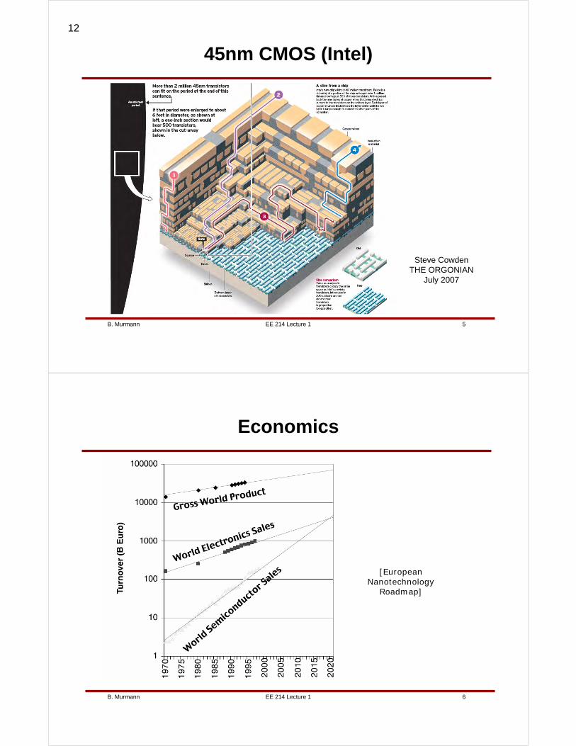
45nm CMOS (Intel)
Steve CowdenTHE ORGONIAN
July 2007
EE 214 Lecture 1B. Murmann 6
Economics
[European Nanotechnology
Roadmap]
12

EE 214 Lecture 1B. Murmann 7
Future Applications
EE 214 Lecture 1B. Murmann 8
Discrete vs. Integrated Circuits
• Minimize transistor count
• Devices usually don't match
• Arbitrary resistor values
• Capacitors 1pF…10mF
• "Unlimited" number of transistors
• Devices match well
• Keep resistors < 10…100k
• Keep capacitors < 10…50pF
Discrete Audio Amplifier Integrated CMOS Audio Amplifier
13
EE 214 Lecture 1B. Murmann 9
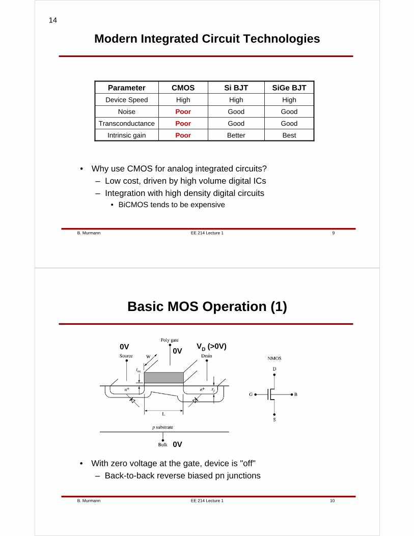
Modern Integrated Circuit Technologies
• Why use CMOS for analog integrated circuits?
– Low cost, driven by high volume digital ICs
– Integration with high density digital circuits• BiCMOS tends to be expensive
BestBetterPoorIntrinsic gain
GoodGoodPoorTransconductance
GoodGoodPoorNoise
HighHighHighDevice Speed
SiGe BJTSi BJTCMOSParameter
EE 214 Lecture 1B. Murmann 10
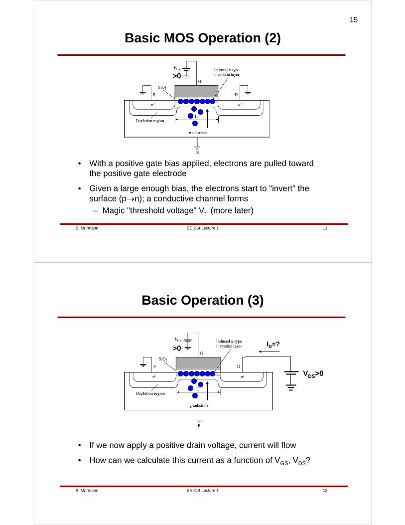
Basic MOS Operation (1)
• With zero voltage at the gate, device is "off"
– Back-to-back reverse biased pn junctions
0V VD (>0V)0V
0V
14
EE 214 Lecture 1B. Murmann 11
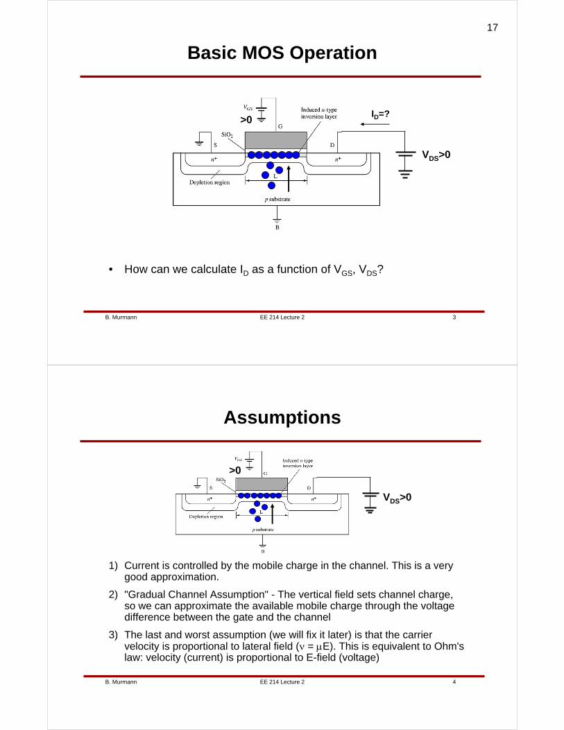
Basic MOS Operation (2)
• With a positive gate bias applied, electrons are pulled toward the positive gate electrode
• Given a large enough bias, the electrons start to "invert" the surface (p→n); a conductive channel forms
– Magic "threshold voltage" Vt (more later)
>0
EE 214 Lecture 1B. Murmann 12
Basic Operation (3)
• If we now apply a positive drain voltage, current will flow
• How can we calculate this current as a function of VGS, VDS?
>0
VDS>0
ID=?
15

EE 214 Lecture 2B. Murmann 1
Lecture 2Common Source Amplifier
Small-Signal Model
Boris MurmannStanford University
Copyright © 2007 by Boris Murmann
EE 214 Lecture 2B. Murmann 2
Overview
• Reading– 3.0 (Amplifier basics), 3.1 (Model selection)
– 3.3.2 (Common source amplifer)
– 1.6.0 - 1.6.5 (Small signal MOS model)
• Introduction
– Today we'll complete our derivation of the basic long-channel MOSFET I-V characteristics. As a next step, we'll use this simple model to construct our first amplifier – a common source stage. Looking at its transfer function, we'll find that treating signals as "small" with respect to the bias conditions allows us to linearize the circuit. Next, we generalize this approach and develop a more universal "plug-and-play" small-signal model for MOS devices that are biased in the active region.
16
EE 214 Lecture 2B. Murmann 3
Basic MOS Operation
• How can we calculate ID as a function of VGS, VDS?
>0
VDS>0
ID=?
EE 214 Lecture 2B. Murmann 4
Assumptions
1) Current is controlled by the mobile charge in the channel. This is a very good approximation.
2) "Gradual Channel Assumption" - The vertical field sets channel charge, so we can approximate the available mobile charge through the voltage difference between the gate and the channel
3) The last and worst assumption (we will fix it later) is that the carrier velocity is proportional to lateral field (ν = μE). This is equivalent to Ohm's law: velocity (current) is proportional to E-field (voltage)
>0
VDS>0
17
EE 214 Lecture 2B. Murmann 5
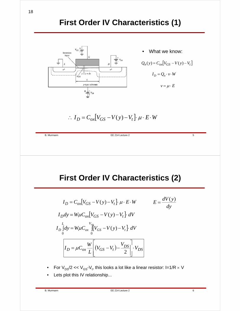
First Order IV Characteristics (1)
• What we know:
[ ]tGSoxn VyVVCyQ −−= )()(
WvQI nD ⋅⋅=
Ev ⋅= μ
[ ] WEVyVVCI tGSoxD ⋅⋅⋅−−=∴ μ)(
EE 214 Lecture 2B. Murmann 6
First Order IV Characteristics (2)
dy
ydVE
)(=[ ] WEVyVVCI tGSoxD ⋅⋅⋅−−= μ)(
[ ] dVVyVVCWdyI tGSoxD ⋅−−= )(μ
[ ]∫ ⋅−−=∫DSV
tGSox
L
D dVVyVVCWdyI00
)(μ
( ) DSDS
tGSoxD VV
VVL
WCI ⋅
⎥⎥⎦
⎤
⎢⎢⎣
⎡−−=
2μ
• For VDS/2 << VGS-Vt, this looks a lot like a linear resistor: I=1/R × V
• Lets plot this IV relationship...
18

EE 214 Lecture 2B. Murmann 7
Plot of First Order IV Curves
• Something is wrong here...
– Current should never decrease with increasing VDS
• What happens when VDS>VGS-Vt?
– VGD = VGS-VDS becomes less than Vt, i.e. no more channel or "pinch off"
VDSID
VGS-Vt
EE 214 Lecture 2B. Murmann 8
Pinch-Off
• Effective voltage across channel is VGS - Vt
– After channel charge goes to 0, there is a high lateral field that ‘sweeps’ the carriers to the drain, and drops the extra voltage (this is a depletion region of the drain junction)
• To first order, current becomes independent of VDS
N N
– V G S +
+ V DS –
y
y = 0 y = L
Q ( y ) , V ( y ) n
Voltage at the end of channelIs fixed at VGS-Vt
19
EE 214 Lecture 2B. Murmann 9
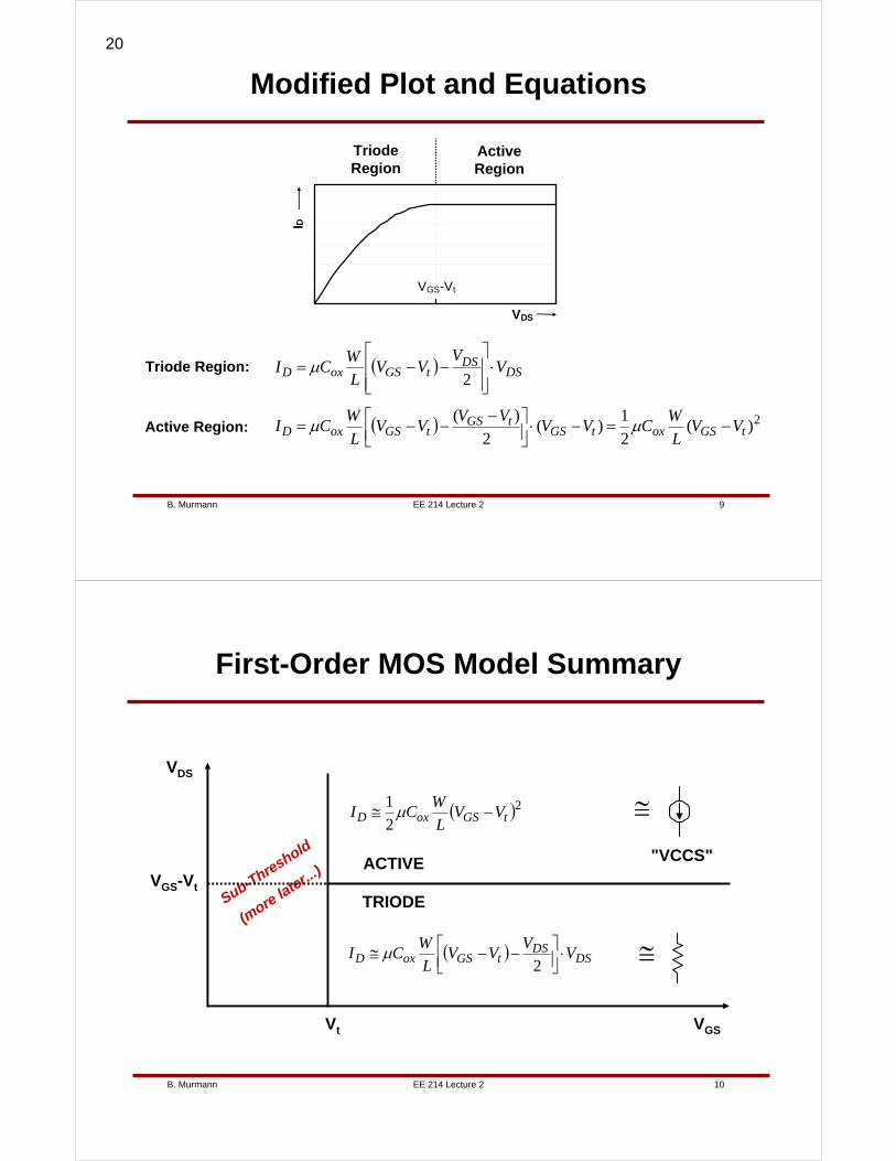
Modified Plot and Equations
VDS
IDVGS-Vt
Triode Region
ActiveRegion
( ) DSDS
tGSoxD VV
VVL
WCI ⋅
⎥⎥⎦
⎤
⎢⎢⎣
⎡−−=
2μTriode Region:
Active Region: ( ) 2)(2
1)(
2
)(tGSoxtGS
tGStGSoxD VV
L
WCVV
VVVV
L
WCI −=−⋅⎥⎦
⎤⎢⎣⎡ −
−−= μμ
EE 214 Lecture 2B. Murmann 10
First-Order MOS Model Summary
( )22
1tGSoxD VV
L
WCI −≅ μ
Sub-Threshold
(more la
ter...)
Vt VGS
VDS
VGS-Vt
ACTIVE
TRIODE
( ) DSDS
tGSoxD VV
VVL
WCI ⋅⎥⎦
⎤⎢⎣⎡ −−≅
2μ
≅
≅
"VCCS"
20

EE 214 Lecture 2B. Murmann 11
Model Accuracy
• The above equations constitute the most basic MOS IV model
– "Long channel model", "quadratic model", "low field model"
• Unfortunately this model doesn't describe modern CMOS devices accurately
– Pushing towards extremely small geometries has resulted in very high electric fields
• Some of the assumptions on slide 4 become invalid
• Other second order dependencies arise
• Nevertheless, we will use this simple model in the first few lectures to develop some basic circuit intuition
– Will fix and refine as we go…
– "Just-in-time" modeling
EE 214 Lecture 2B. Murmann 12
Let's Build Our First Amplifier
• One way to amplify– Convert input voltage to current using voltage controlled
current source (VCCS)– Convert back to voltage using a resistor (R)
• "Voltage gain" = ΔVout/ΔVin
– Product of the V-I and I-V conversion factors
21
EE 214 Lecture 2B. Murmann 13
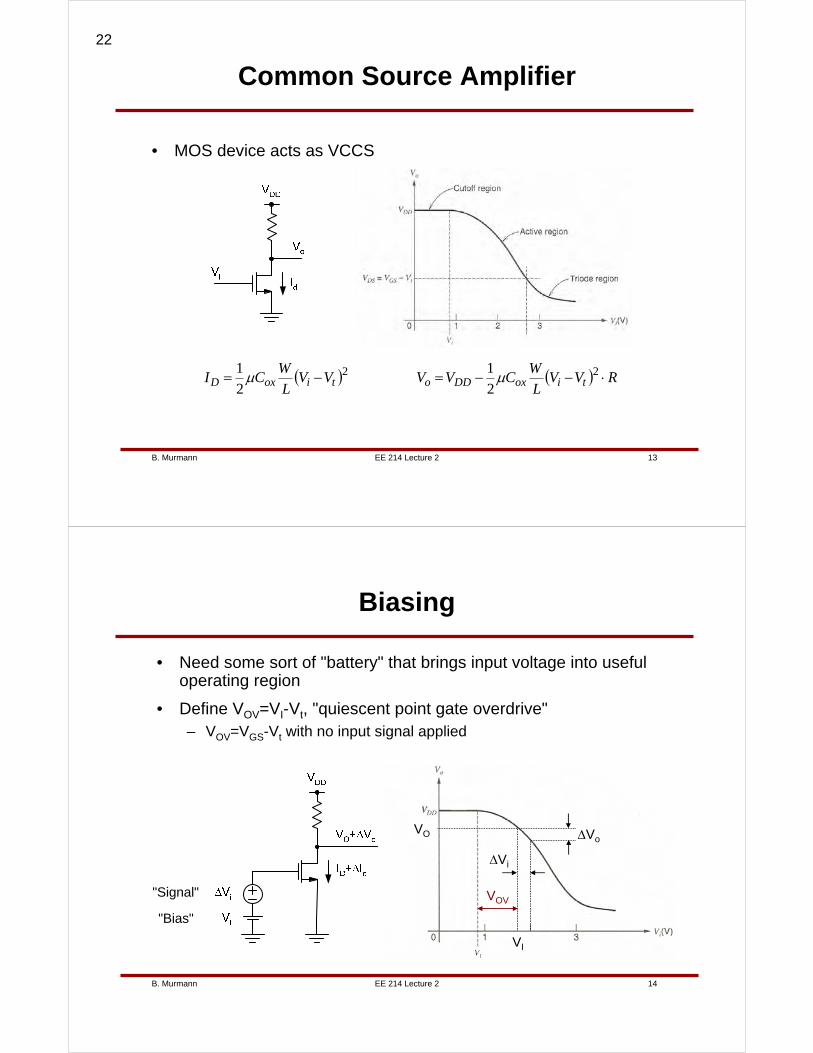
Common Source Amplifier
• MOS device acts as VCCS
( )22
1tioxD VV
L
WCI −= μ ( ) RVV
L
WCVV tioxDDo ⋅−−= 2
2
1 μ
EE 214 Lecture 2B. Murmann 14
Biasing
• Need some sort of "battery" that brings input voltage into useful operating region
• Define VOV=VI-Vt, "quiescent point gate overdrive"– VOV=VGS-Vt with no input signal applied
"Bias"
"Signal"
VI
ΔVo
ΔVi
VO
VOV
22
EE 214 Lecture 2B. Murmann 15
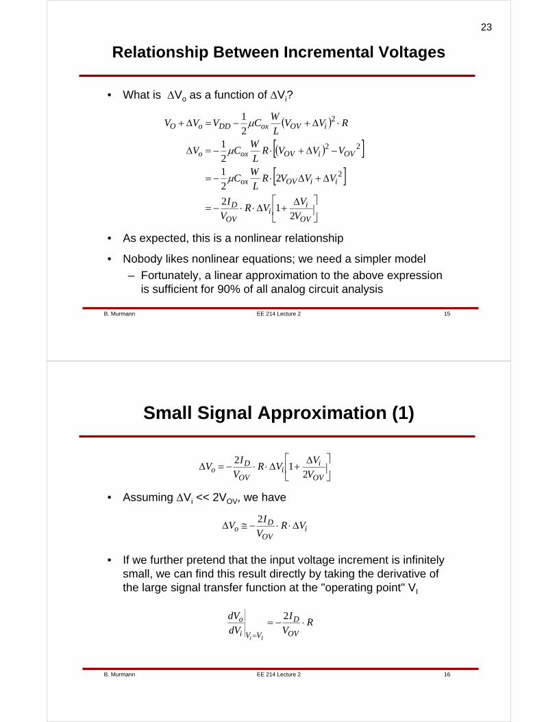
Relationship Between Incremental Voltages
• What is ΔVo as a function of ΔVi?
( )
( )[ ][ ]
⎥⎦
⎤⎢⎣
⎡ Δ+Δ⋅⋅−=
Δ+Δ⋅−=
−Δ+⋅−=Δ
⋅Δ+−=Δ+
OV
ii
OV
D
iiOVox
OViOVoxo
iOVoxDDoO
V
VVR
V
I
VVVRL
WC
VVVRL
WCV
RVVL
WCVVV
21
2
22
12
12
1
2
22
2
μ
μ
μ
• As expected, this is a nonlinear relationship
• Nobody likes nonlinear equations; we need a simpler model
– Fortunately, a linear approximation to the above expression is sufficient for 90% of all analog circuit analysis
EE 214 Lecture 2B. Murmann 16
Small Signal Approximation (1)
• Assuming ΔVi << 2VOV, we have
⎥⎦
⎤⎢⎣
⎡ Δ+Δ⋅⋅−=Δ
OV
ii
OV
Do V
VVR
V
IV
21
2
iOV
Do VR
V
IV Δ⋅⋅−≅Δ
2
• If we further pretend that the input voltage increment is infinitely small, we can find this result directly by taking the derivative of the large signal transfer function at the "operating point" VI
RV
I
dV
dV
OV
D
VVi
o
Ii
⋅−==
2
23
EE 214 Lecture 2B. Murmann 17
Small Signal Approximation (2)
• Graphical illustration:
VI
VO
VOV
dVo/dVi
• The slope of the above tangent is the so called "small signal gain" of our amplifier
EE 214 Lecture 2B. Murmann 18
Small Signal MOS Model
• Fortunately we don't have to repeat this analysis for every single circuit we build
• Instead, we derive a linearized circuit model for the MOS transistor and plug it into arbitrary circuits
24
EE 214 Lecture 2B. Murmann 19
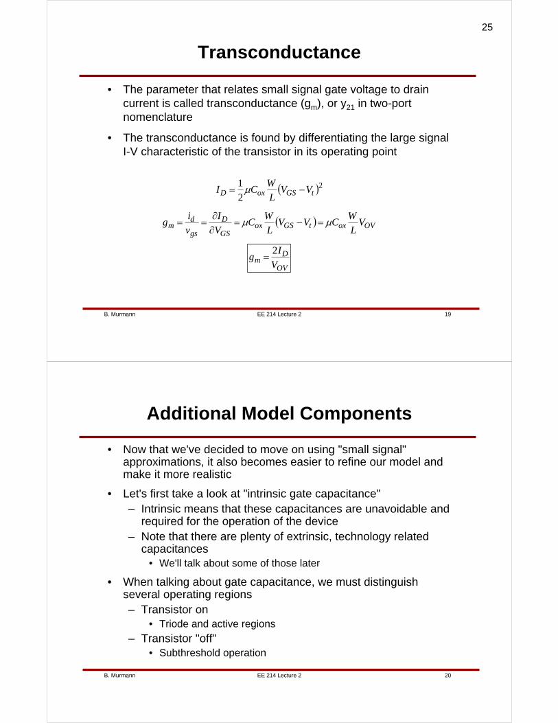
Transconductance
• The parameter that relates small signal gate voltage to drain current is called transconductance (gm), or y21 in two-port nomenclature
• The transconductance is found by differentiating the large signal I-V characteristic of the transistor in its operating point
( )22
1tGSoxD VV
L
WCI −= μ
( ) OVoxtGSoxGS
D
gs
dm V
L
WCVV
L
WC
V
I
v
ig μμ =−=
∂∂
==
OV
Dm V
Ig
2=
EE 214 Lecture 2B. Murmann 20
Additional Model Components
• Now that we've decided to move on using "small signal" approximations, it also becomes easier to refine our model and make it more realistic
• Let's first take a look at "intrinsic gate capacitance"– Intrinsic means that these capacitances are unavoidable and
required for the operation of the device– Note that there are plenty of extrinsic, technology related
capacitances• We'll talk about some of those later
• When talking about gate capacitance, we must distinguish several operating regions– Transistor on
• Triode and active regions
– Transistor "off"• Subthreshold operation
25
EE 214 Lecture 2B. Murmann 21
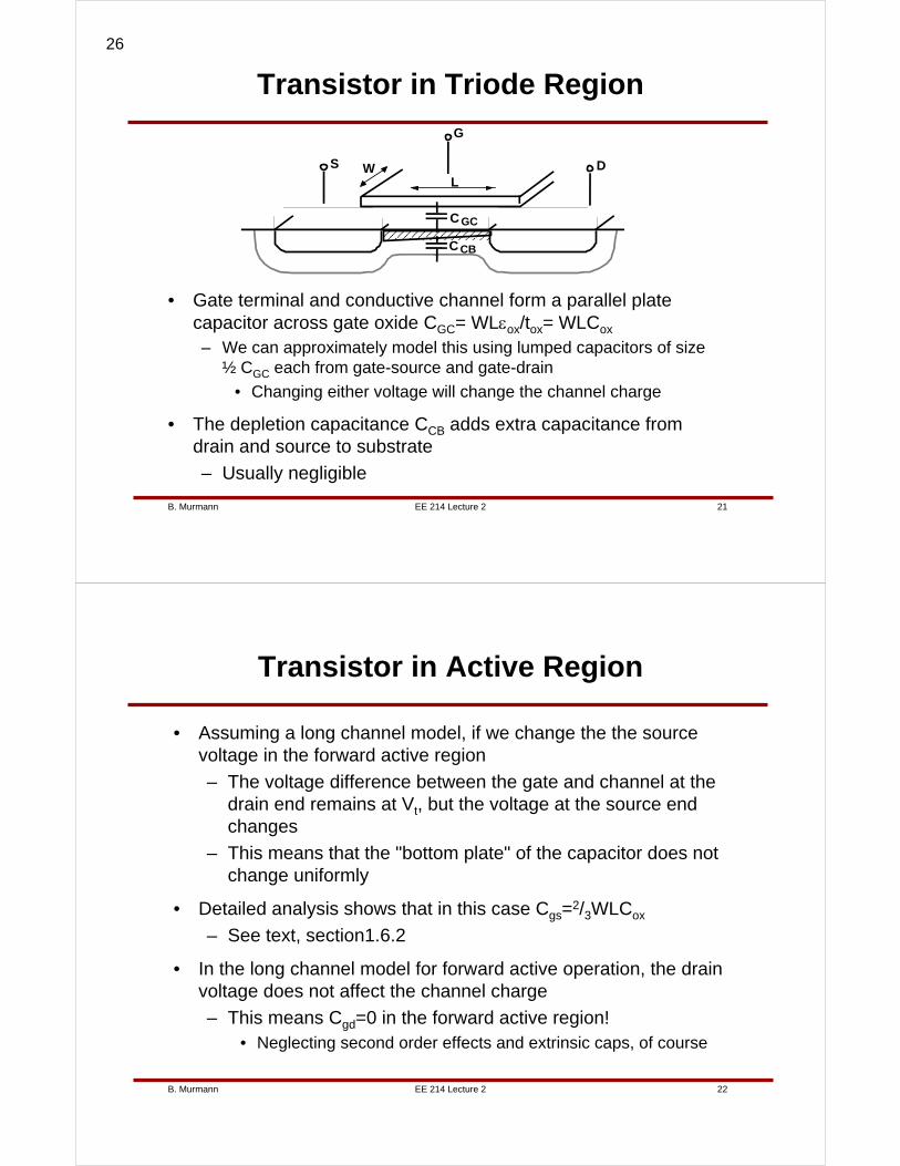
Transistor in Triode Region
• Gate terminal and conductive channel form a parallel plate capacitor across gate oxide CGC= WLεox/tox= WLCox
– We can approximately model this using lumped capacitors of size ½ CGC each from gate-source and gate-drain
• Changing either voltage will change the channel charge
• The depletion capacitance CCB adds extra capacitance from drain and source to substrate
– Usually negligible
L
S D W
G
C GC
C CB
EE 214 Lecture 2B. Murmann 22
Transistor in Active Region
• Assuming a long channel model, if we change the the source voltage in the forward active region
– The voltage difference between the gate and channel at the drain end remains at Vt, but the voltage at the source end changes
– This means that the "bottom plate" of the capacitor does not change uniformly
• Detailed analysis shows that in this case Cgs=2/3WLCox
– See text, section1.6.2
• In the long channel model for forward active operation, the drain voltage does not affect the channel charge
– This means Cgd=0 in the forward active region!• Neglecting second order effects and extrinsic caps, of course
26
EE 214 Lecture 2B. Murmann 23
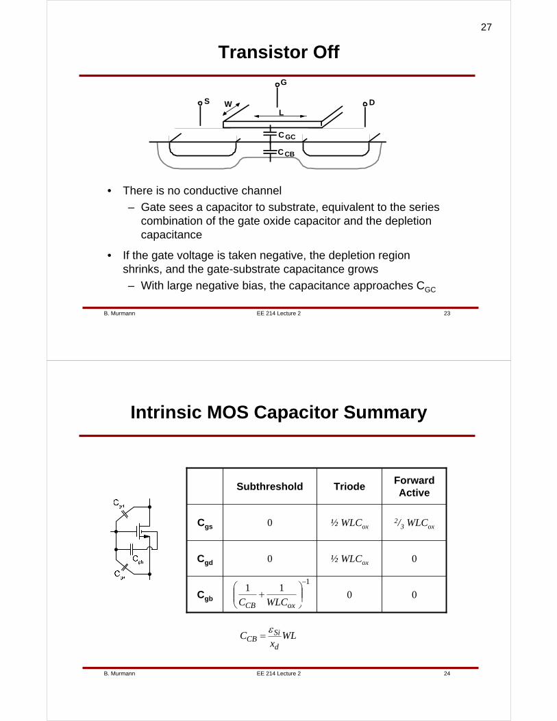
Transistor Off
• There is no conductive channel
– Gate sees a capacitor to substrate, equivalent to the series combination of the gate oxide capacitor and the depletion capacitance
• If the gate voltage is taken negative, the depletion region shrinks, and the gate-substrate capacitance grows
– With large negative bias, the capacitance approaches CGC
L
S D W
G
C GC
C CB
EE 214 Lecture 2B. Murmann 24
Intrinsic MOS Capacitor Summary
00Cgb
0½ WLCox0Cgd
2/3 WLCox½ WLCox0Cgs
Forward Active
TriodeSubthreshold
111
−
⎟⎟⎠
⎞⎜⎜⎝
⎛+
oxCB WLCC
WLx
Cd
SiCB
ε=
27
EE 214 Lecture 2B. Murmann 25
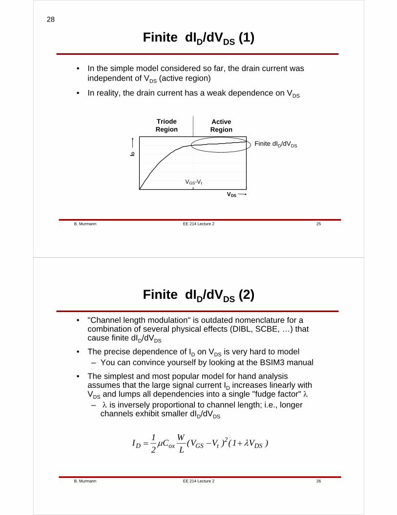
Finite dID/dVDS (1)
• In the simple model considered so far, the drain current was independent of VDS (active region)
• In reality, the drain current has a weak dependence on VDS
VDS
ID
VGS-Vt
Triode Region
ActiveRegion
Finite dID/dVDS
EE 214 Lecture 2B. Murmann 26
Finite dID/dVDS (2)
• "Channel length modulation" is outdated nomenclature for a combination of several physical effects (DIBL, SCBE, …) that cause finite dID/dVDS
• The precise dependence of ID on VDS is very hard to model– You can convince yourself by looking at the BSIM3 manual
• The simplest and most popular model for hand analysis assumes that the large signal current ID increases linearly with VDS and lumps all dependencies into a single "fudge factor" λ– λ is inversely proportional to channel length; i.e., longer
channels exhibit smaller dID/dVDS
)V1()VV(L
WC
2
1I DS
2tGSoxD λμ +−=
28
EE 214 Lecture 2B. Murmann 27
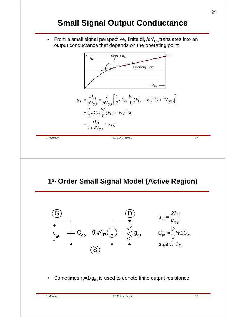
Small Signal Output Conductance
• From a small signal perspective, finite dID/dVDS translates into an output conductance that depends on the operating point
DDS
D
2tGSox
DS2
tGSoxDSDS
Dds
IV1
I
)VV(L
WC
2
1
)V1()VV(L
WC
2
1
dV
d
dV
dIg
λλλ
λμ
λμ
≅+
=
⋅−=
⎥⎦⎤
⎢⎣⎡ +−==
VDS
ID
Operating Point
Slope = gds
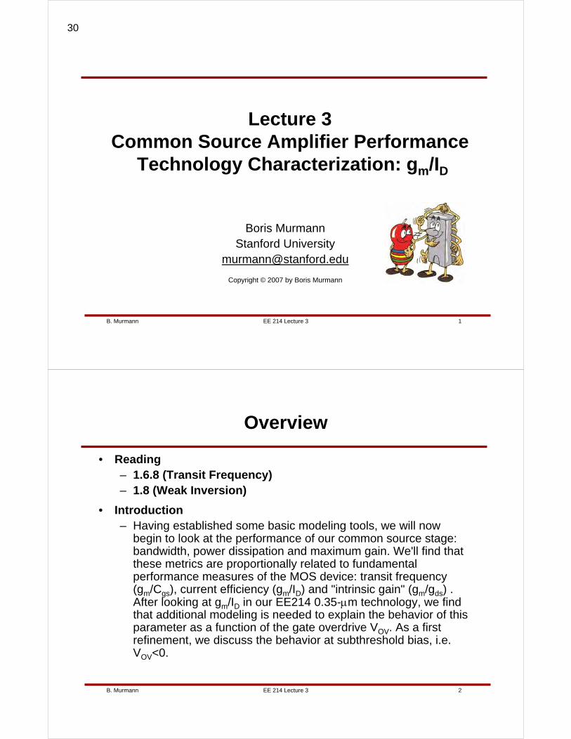
EE 214 Lecture 2B. Murmann 28
1st Order Small Signal Model (Active Region)
Dds
oxgs
OV
Dm
Ig
WLC3
2C
V
I2g
⋅≅
=
=
λ
• Sometimes ro=1/gds is used to denote finite output resistance
29
EE 214 Lecture 3B. Murmann 1
Lecture 3Common Source Amplifier Performance
Technology Characterization: gm/ID
Boris MurmannStanford University
Copyright © 2007 by Boris Murmann
EE 214 Lecture 3B. Murmann 2
Overview
• Reading– 1.6.8 (Transit Frequency)– 1.8 (Weak Inversion)
• Introduction– Having established some basic modeling tools, we will now
begin to look at the performance of our common source stage: bandwidth, power dissipation and maximum gain. We'll find that these metrics are proportionally related to fundamental performance measures of the MOS device: transit frequency (gm/Cgs), current efficiency (gm/ID) and "intrinsic gain" (gm/gds) . After looking at gm/ID in our EE214 0.35-μm technology, we find that additional modeling is needed to explain the behavior of this parameter as a function of the gate overdrive VOV. As a first refinement, we discuss the behavior at subthreshold bias, i.e. VOV<0.
30
EE 214 Lecture 3B. Murmann 3
Common Source Amplifier Revisited
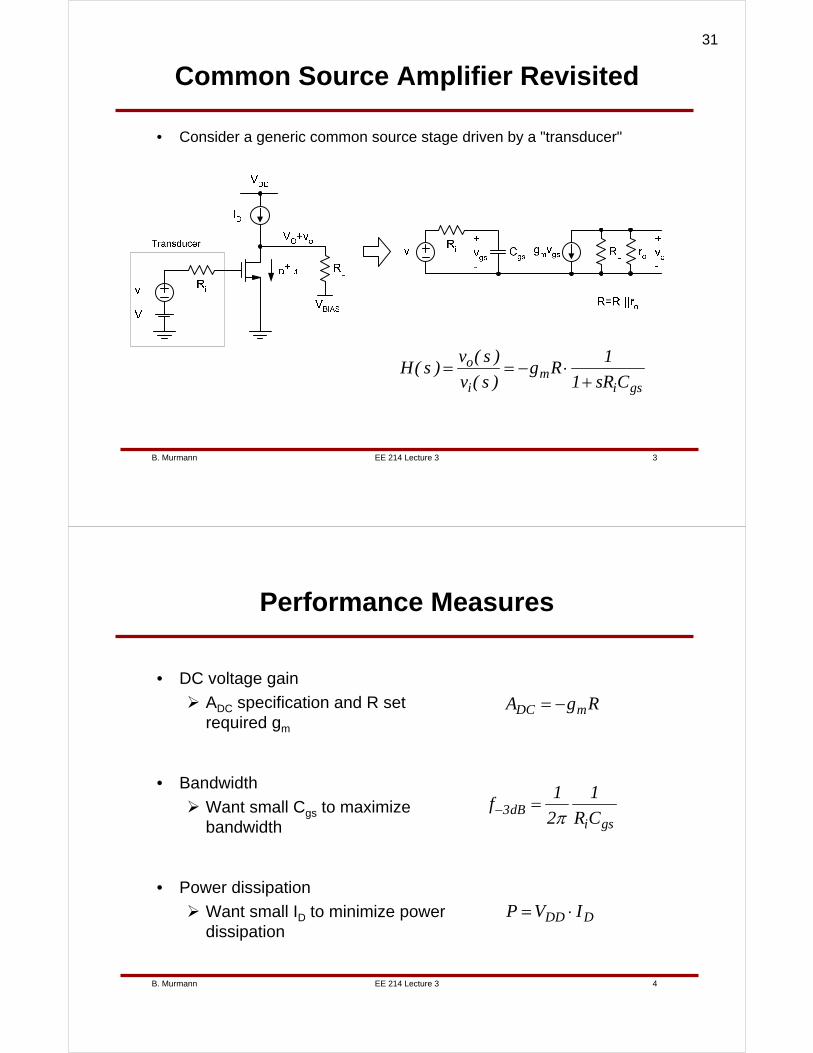
• Consider a generic common source stage driven by a "transducer"
gsim
i
o
CsR1
1Rg
)s(v
)s(v)s(H
+⋅−==
EE 214 Lecture 3B. Murmann 4
Performance Measures
RgA mDC −=• DC voltage gain
ADC specification and R set required gm
• Bandwidth
Want small Cgs to maximize bandwidth
• Power dissipation
Want small ID to minimize power dissipation
gsidB3 CR
1
2
1f
π=−
DDD IVP ⋅=
31
EE 214 Lecture 3B. Murmann 5
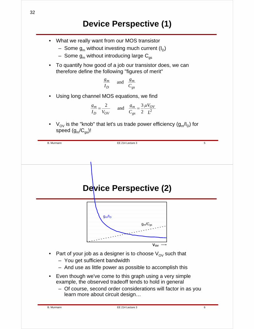
Device Perspective (1)
• What we really want from our MOS transistor
– Some gm without investing much current (ID)
– Some gm without introducing large Cgs
• To quantify how good of a job our transistor does, we can therefore define the following "figures of merit"
gs
m
D
m
C
g
I
gand
• Using long channel MOS equations, we find
22
3and
2
L
V
C
g
VI
g OV
gs
m
OVD
m μ==
• VOV is the "knob" that let's us trade power efficiency (gm/ID) for speed (gm/Cgs)!
EE 214 Lecture 3B. Murmann 6
Device Perspective (2)
• Part of your job as a designer is to choose VOV such that– You get sufficient bandwidth– And use as little power as possible to accomplish this
• Even though we've come to this graph using a very simple example, the observed tradeoff tends to hold in general– Of course, second order considerations will factor in as you
learn more about circuit design…
VOV
gm/ID
gm/Cgs
32
EE 214 Lecture 3B. Murmann 7
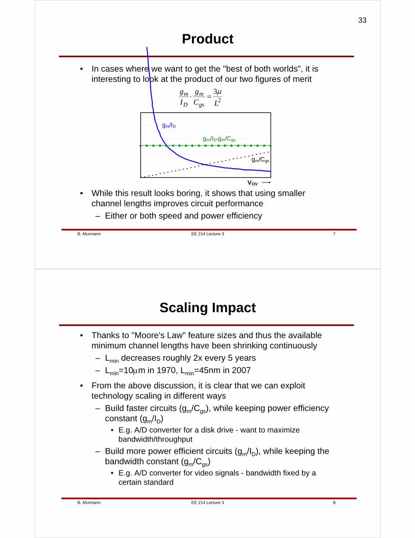
Product
• In cases where we want to get the "best of both worlds", it is interesting to look at the product of our two figures of merit
VOV
gm/ID
gm/Cgs
gm/ID*gm/Cgs
23
LC
g
I
g
gs
m
D
m μ=⋅
• While this result looks boring, it shows that using smaller channel lengths improves circuit performance
– Either or both speed and power efficiency
EE 214 Lecture 3B. Murmann 8
Scaling Impact
• Thanks to "Moore's Law" feature sizes and thus the available minimum channel lengths have been shrinking continuously
– Lmin decreases roughly 2x every 5 years
– Lmin=10μm in 1970, Lmin=45nm in 2007
• From the above discussion, it is clear that we can exploit technology scaling in different ways
– Build faster circuits (gm/Cgs), while keeping power efficiency constant (gm/ID)
• E.g. A/D converter for a disk drive - want to maximize bandwidth/throughput
– Build more power efficient circuits (gm/ID), while keeping the bandwidth constant (gm/Cgs)
• E.g. A/D converter for video signals - bandwidth fixed by a certain standard
33
EE 214 Lecture 3B. Murmann 9
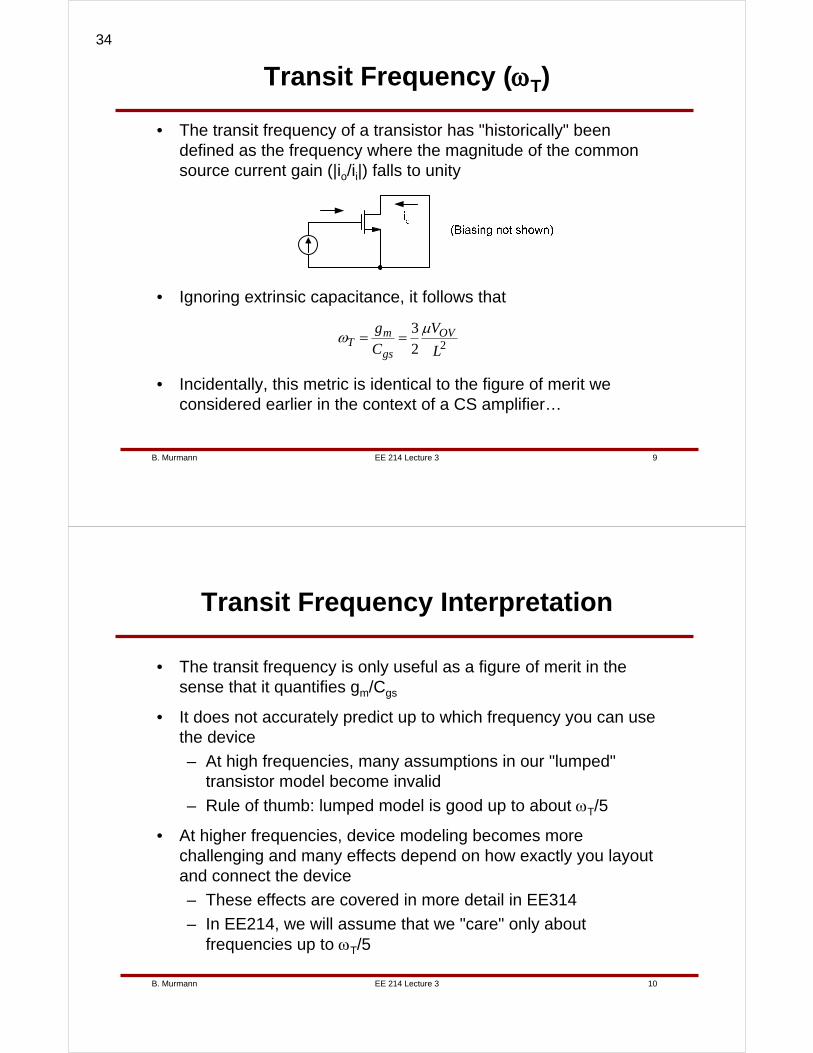
Transit Frequency (ωT)
• The transit frequency of a transistor has "historically" been defined as the frequency where the magnitude of the common source current gain (|io/ii|) falls to unity
• Ignoring extrinsic capacitance, it follows that
22
3
L
V
C
g OV
gs
mT
μω ==
• Incidentally, this metric is identical to the figure of merit weconsidered earlier in the context of a CS amplifier…
EE 214 Lecture 3B. Murmann 10
Transit Frequency Interpretation
• The transit frequency is only useful as a figure of merit in thesense that it quantifies gm/Cgs
• It does not accurately predict up to which frequency you can usethe device
– At high frequencies, many assumptions in our "lumped" transistor model become invalid
– Rule of thumb: lumped model is good up to about ωT/5
• At higher frequencies, device modeling becomes more challenging and many effects depend on how exactly you layout and connect the device
– These effects are covered in more detail in EE314
– In EE214, we will assume that we "care" only about frequencies up to ωT/5
34
EE 214 Lecture 3B. Murmann 11
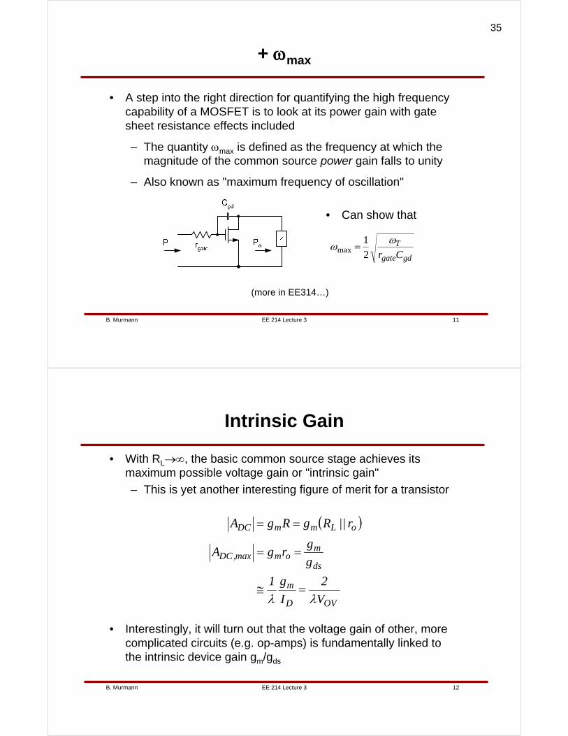
+ ωmax
• Can show that
gdgate
T
Cr
ωω2
1max =
• A step into the right direction for quantifying the high frequency capability of a MOSFET is to look at its power gain with gate sheet resistance effects included
– The quantity ωmax is defined as the frequency at which the magnitude of the common source power gain falls to unity
– Also known as "maximum frequency of oscillation"
(more in EE314…)
EE 214 Lecture 3B. Murmann 12
Intrinsic Gain
• With RL→∞, the basic common source stage achieves its maximum possible voltage gain or "intrinsic gain"
– This is yet another interesting figure of merit for a transistor
( )
OVD
m
ds
mommax,DC
oLmmDC
V
2
I
g1
g
grgA
r||RgRgA
λλ=≅
==
==
• Interestingly, it will turn out that the voltage gain of other, more complicated circuits (e.g. op-amps) is fundamentally linked to the intrinsic device gain gm/gds
35
EE 214 Lecture 3B. Murmann 13
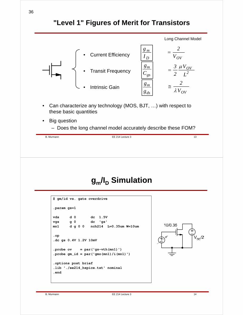
"Level 1" Figures of Merit for Transistors
ds
m
g
g
• Current Efficiency
• Transit Frequency
• Intrinsic Gain
D
m
I
g
• Can characterize any technology (MOS, BJT, …) with respect to these basic quantities
• Big question
– Does the long channel model accurately describe these FOM?
OVV
2=
2OV
L
V
2
3 μ=
Long Channel Model
gs
m
C
g
OVV
2
λ≅
EE 214 Lecture 3B. Murmann 14
gm/ID Simulation
$ gm/id vs. gate overdrive
.param gs=1
vds d 0 dc 1.5Vvgs g 0 dc 'gs'mn1 d g 0 0 nch214 L=0.35um W=10um
.op
.dc gs 0.4V 1.2V 10mV
.probe ov = par('gs-vth(mn1)')
.probe gm_id = par('gmo(mn1)/i(mn1)')
.options post brief
.lib './ee214_hspice.txt' nominal
.end
36
EE 214 Lecture 3B. Murmann 15
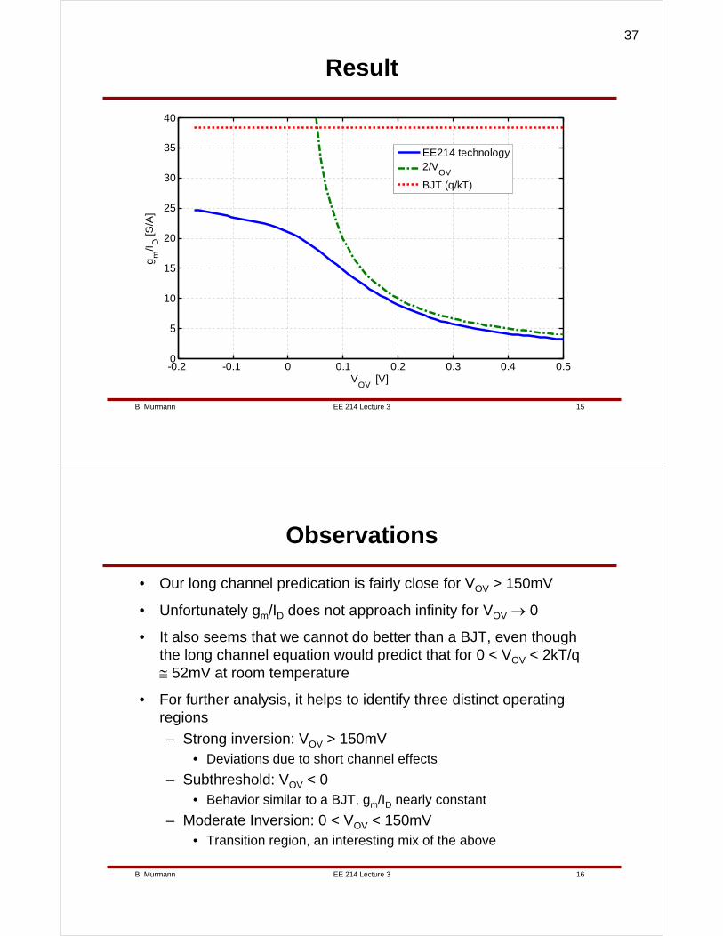
Result
-0.2 -0.1 0 0.1 0.2 0.3 0.4 0.50
5
10
15
20
25
30
35
40
VOV
[V]
gm
/ID
[S/A
]
EE214 technology2/V
OV
BJT (q/kT)
EE 214 Lecture 3B. Murmann 16
Observations
• Our long channel predication is fairly close for VOV > 150mV
• Unfortunately gm/ID does not approach infinity for VOV → 0
• It also seems that we cannot do better than a BJT, even though the long channel equation would predict that for 0 < VOV < 2kT/q ≅ 52mV at room temperature
• For further analysis, it helps to identify three distinct operating regions
– Strong inversion: VOV > 150mV• Deviations due to short channel effects
– Subthreshold: VOV < 0 • Behavior similar to a BJT, gm/ID nearly constant
– Moderate Inversion: 0 < VOV < 150mV• Transition region, an interesting mix of the above
37
EE 214 Lecture 3B. Murmann 17
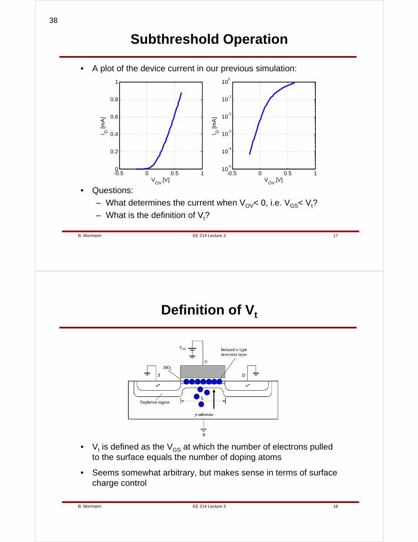
Subthreshold Operation
• Questions:
– What determines the current when VOV< 0, i.e. VGS< Vt?
– What is the definition of Vt?
• A plot of the device current in our previous simulation:
-0.5 0 0.5 10
0.2
0.4
0.6
0.8
1
VOV
[V]
I D [m
A]
-0.5 0 0.5 110
-5
10-4
10-3
10-2
10-1
100
VOV
[V]
I D [m
A]
EE 214 Lecture 3B. Murmann 18
Definition of Vt
• Vt is defined as the VGS at which the number of electrons pulled to the surface equals the number of doping atoms
• Seems somewhat arbitrary, but makes sense in terms of surface charge control
38
EE 214 Lecture 3B. Murmann 19
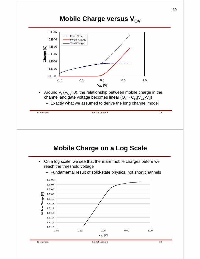
Mobile Charge versus VOV
• Around Vt (VOV=0), the relationship between mobile charge in the channel and gate voltage becomes linear (Qn ~ Cox[VGS-Vt])
– Exactly what we assumed to derive the long channel model
0.E+00
1.E-07
2.E-07
3.E-07
4.E-07
5.E-07
6.E-07
-1.0 -0.5 0.0 0.5 1.0
VOV [V]
Ch
arg
e [
C]
Fixed Charge
Mobile Charge
Total Charge
EE 214 Lecture 3B. Murmann 20
Mobile Charge on a Log Scale
• On a log scale, we see that there are mobile charges before we reach the threshold voltage
– Fundamental result of solid-state physics, not short channels
1.E-16
1.E-15
1.E-14
1.E-13
1.E-12
1.E-11
1.E-10
1.E-09
1.E-08
1.E-07
1.E-06
-1.00 -0.50 0.00 0.50 1.00
VOV [V]
Mo
bil
e C
har
ge
[C]
39
EE 214 Lecture 3B. Murmann 21
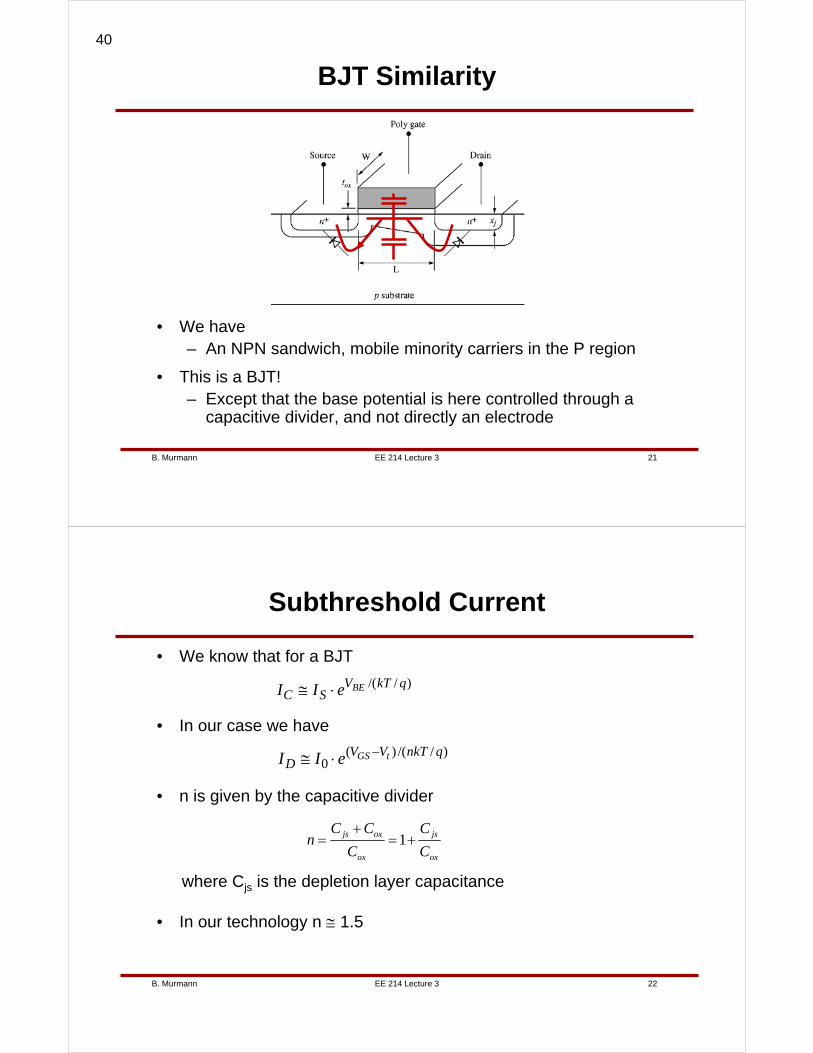
BJT Similarity
• We have– An NPN sandwich, mobile minority carriers in the P region
• This is a BJT!– Except that the base potential is here controlled through a
capacitive divider, and not directly an electrode
EE 214 Lecture 3B. Murmann 22
Subthreshold Current
• We know that for a BJT
)//( qkTVSC
BEeII ⋅≅
• In our case we have
)//()(0
qnkTVVD
tGSeII −⋅≅
• n is given by the capacitive divider
ox
js
ox
oxjs
C
C
C
CCn +=
+= 1
where Cjs is the depletion layer capacitance
• In our technology n ≅ 1.5
40
EE 214 Lecture 3B. Murmann 23
Subthreshold Transconductance
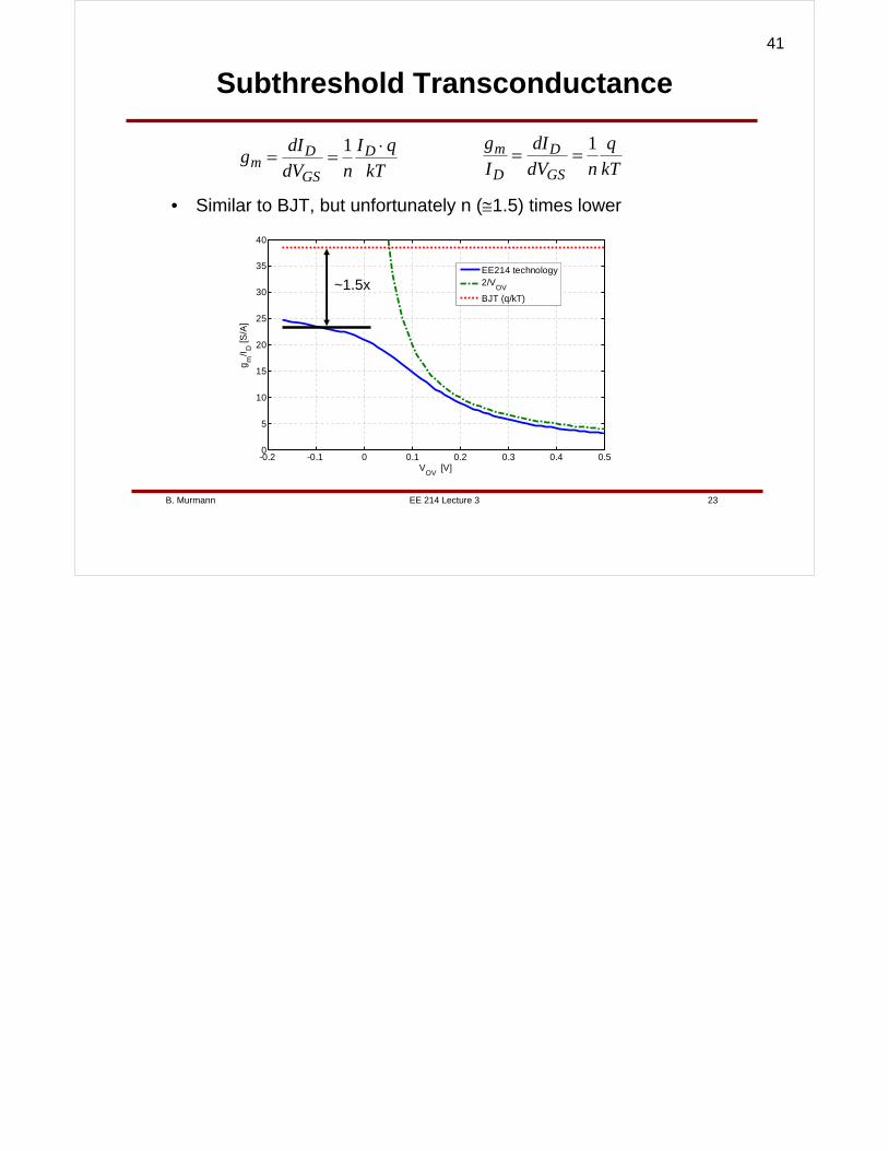
• Similar to BJT, but unfortunately n (≅1.5) times lower
kT
qI
ndV
dIg D
GS
Dm
⋅==
1kT
q
ndV
dI
I
g
GS
D
D
m 1==
-0.2 -0.1 0 0.1 0.2 0.3 0.4 0.50
5
10
15
20
25
30
35
40
VOV
[V]
gm
/ID
[S/A
]
EE214 technology2/V
OV
BJT (q/kT)~1.5x
41
EE 214 Lecture 4B. Murmann 1
Lecture 4Short Channel Effects
Technology Characterization: fT, gm/gds
Boris MurmannStanford University
Copyright © 2007 by Boris Murmann
EE 214 Lecture 4B. Murmann 2
Overview
• Reading
– 1.7 (Short Channel Effects)
• Introduction
– Today, we continue our discussion on gm/ID modeling in a MOS device. We explain the remaining discrepancies with the long channel model and then move on to an examination of gm/Cgs (fT) and gm/gds. In conclusion, we find that the long channel model cannot accurately predict either performance metric we care about (gm/ID, gm/Cgs and gm/gds). As a solution to this problem, we will explore a chart-based design methodology in the remainder of this course.
42
EE 214 Lecture 4B. Murmann 3
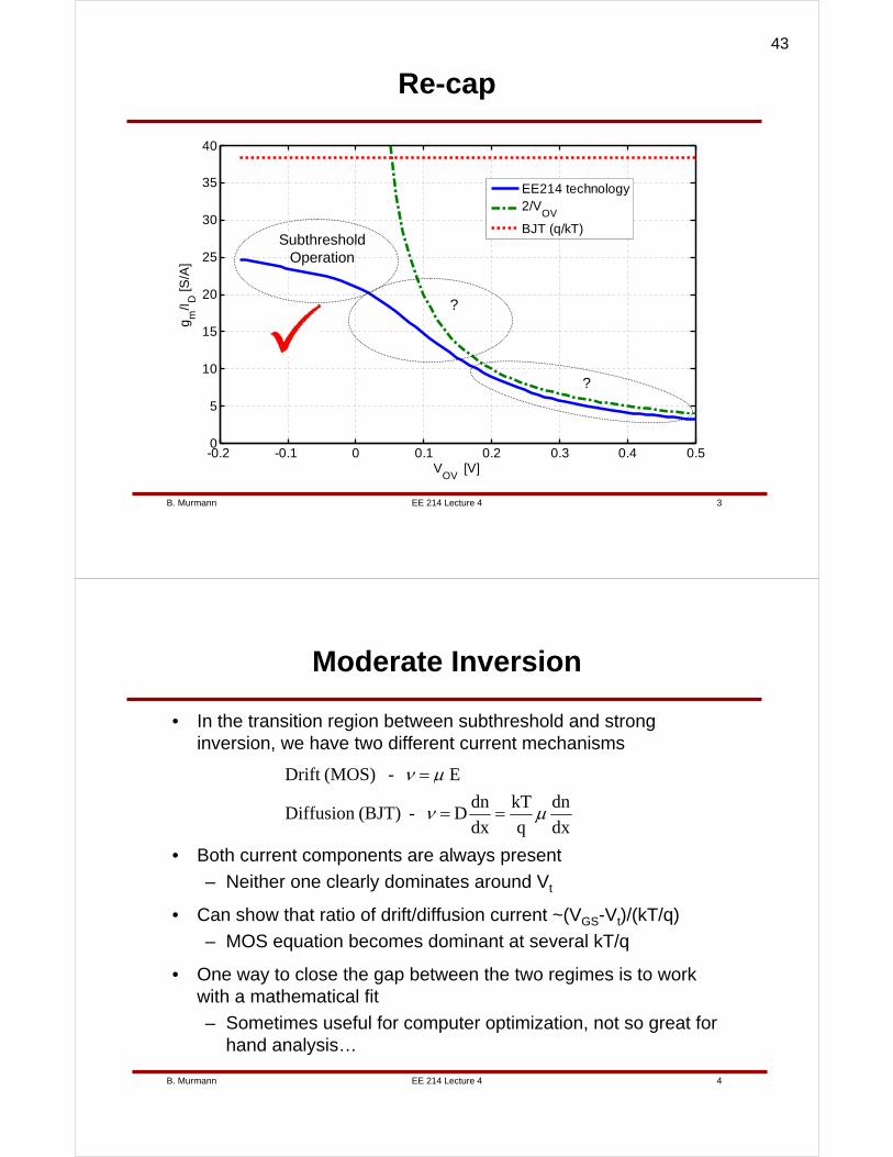
Re-cap
-0.2 -0.1 0 0.1 0.2 0.3 0.4 0.50
5
10
15
20
25
30
35
40
VOV
[V]
gm
/ID
[S/A
]
EE214 technology2/V
OV
BJT (q/kT)Subthreshold
Operation
?
?
EE 214 Lecture 4B. Murmann 4
Moderate Inversion
• In the transition region between subthreshold and strong inversion, we have two different current mechanisms
dx
dn
q
kT
dx
dnD - (BJT)Diffusion
E - (MOS)Drift
μν
μν
==
=
• Both current components are always present
– Neither one clearly dominates around Vt
• Can show that ratio of drift/diffusion current ~(VGS-Vt)/(kT/q)
– MOS equation becomes dominant at several kT/q
• One way to close the gap between the two regimes is to work with a mathematical fit
– Sometimes useful for computer optimization, not so great for hand analysis…
43
EE 214 Lecture 4B. Murmann 5
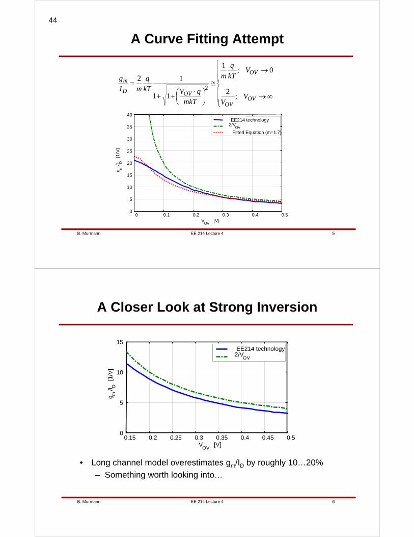
A Curve Fitting Attempt
⎪⎪
⎩
⎪⎪
⎨
⎧
∞→
→
≅
⎟⎠⎞
⎜⎝⎛ ⋅
++
=
OVOV
OV
OVD
m
VV
VkT
q
m
mkTqVkT
q
mI
g
;2
0;1
11
122
0 0.1 0.2 0.3 0.4 0.50
5
10
15
20
25
30
35
40
VOV
[V]
g m/I D
[1/V
]EE214 technology
2/VOV
Fitted Equation (m=1.7)
EE 214 Lecture 4B. Murmann 6
A Closer Look at Strong Inversion
• Long channel model overestimates gm/ID by roughly 10…20%
– Something worth looking into…
0.15 0.2 0.25 0.3 0.35 0.4 0.45 0.50
5
10
15
VOV
[V]
g m/I D
[1/V
]
EE214 technology2/V
OV
44
EE 214 Lecture 4B. Murmann 7
Short Channel Effects
• Velocity saturation due to high lateral field
• Mobility degradation due to high vertical field
• Vt dependence on channel length and width
• ro = f(VDS)
• …
• We will limit the discussion in EE214 to the first two aspects of the above list
– Focus on qualitative understanding, since we will not factor these effects into our hand calculations
EE 214 Lecture 4B. Murmann 8
Velocity Saturation (1)
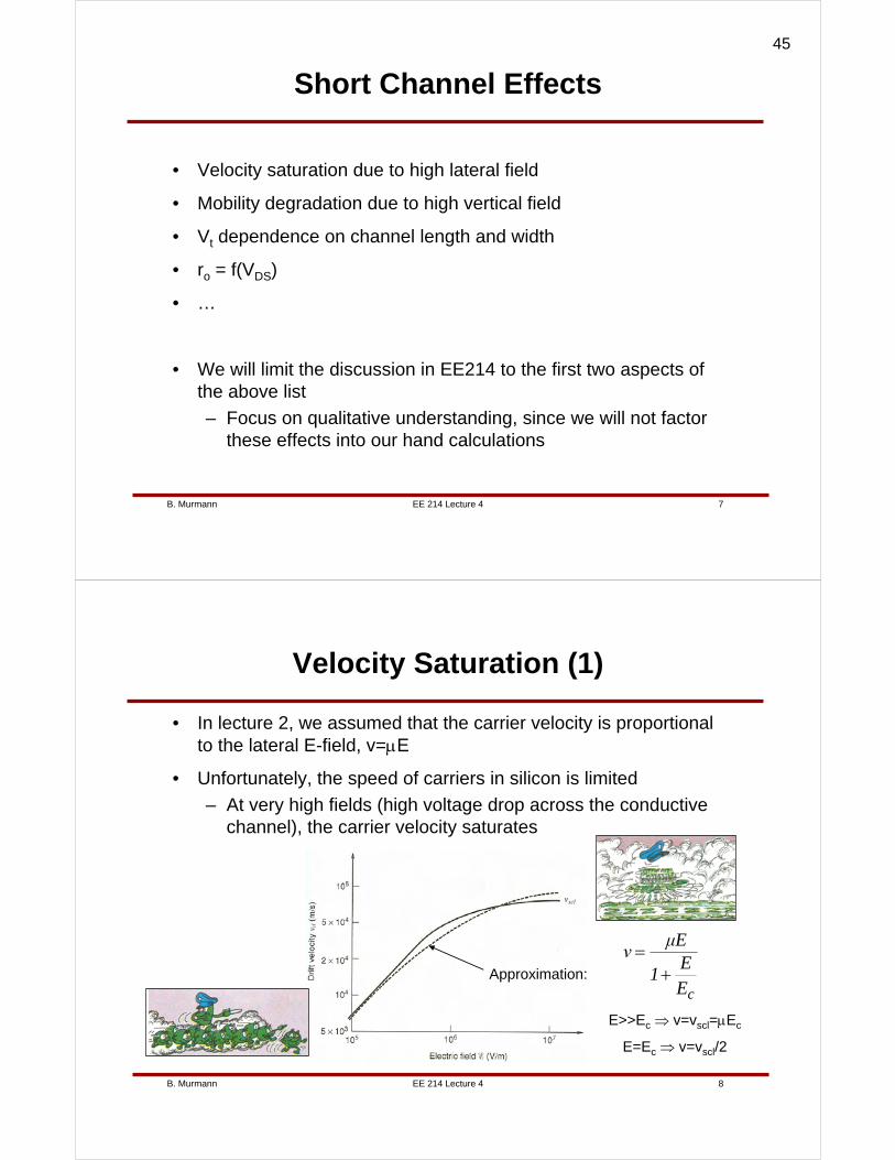
• In lecture 2, we assumed that the carrier velocity is proportional to the lateral E-field, v=μE
• Unfortunately, the speed of carriers in silicon is limited
– At very high fields (high voltage drop across the conductive channel), the carrier velocity saturates
Approximation:
EE
1
μE ν
c+
=
E>>Ec ⇒ v=vscl=μEc
E=Ec ⇒ v=vscl/2
45

EE 214 Lecture 4B. Murmann 9
Velocity Saturation (2)
• It is important to distinguish various regions in the above plot
– Low field, the long channel equations still hold
– Moderate field, the long channel equations become somewhat inaccurate
– Very high field across the conducting channel – the velocity saturates completely and becomes essentially constant (vscl)
• To get some feel for latter two cases, let's first estimate the E field using simple long channel physics
• In the forward active region, at pinch-off, the lateral field across the channel is
m
V.
m.
mVe.g.
L
V E OV 610570
350
200⋅==
μ
EE 214 Lecture 4B. Murmann 10
Field Estimates
• In our 0.35μm technology, we have for an NMOS device
m
V.
Vsm
.
sm
101.73
v E
5
sclc
62
1026
0280
⋅=⋅
==μ
• The above example shows that an 0.35μm NMOS device at VOV=200mV does not operate anywhere near the critical field (E=0.57·106 << Ec)
• How about, e.g., 0.13μm?
m
V.
m.
mV E 61051
130
200⋅==
μ• Still not too bad…
46

EE 214 Lecture 4B. Murmann 11
Short Channel Equation
• Bottom line is that most existing and future MOS analog circuitsare impaired, but not completely limited by velocity saturation
– The digital folks will tell you a different story• Why?
• A simple equation that captures the moderate deviation from the long channel forward active drain current is (see text)
( )OVc
OVcOVox
c
OVOVoxD
VLE
VLEV
L
WC
LEV
VL
WCI
+⋅
⋅≅
⎟⎟⎠
⎞⎜⎜⎝
⎛+
⋅≅
μ
μ
2
1
1
1
2
1 2
"Parallel Combination"
EE 214 Lecture 4B. Murmann 12
Typical Values for EcL
• As long as VOV is "much less" than these voltages, the above simplified equation holds with reasonable accuracy
• We can use these numbers to check our earlier simulation data for gm/ID. With the correction factor, we have
2.4V0.6V0.13μm
8V2 V0.35μm
PMOSNMOS
902
220
1
12
1
12.
V.V.g.e
LEVVI
g
OVOV
c
OVOVD
m ⋅≅⎟⎠⎞
⎜⎝⎛ +⋅
⎟⎟⎠
⎞⎜⎜⎝
⎛+
⋅≅
• Reasonable agreement with simulation data on slide 6
(Note that this expression is found by using 1.223 and 1.233 in the text, and not from the approximate ID expression on the previous slide)
47

EE 214 Lecture 4B. Murmann 13
Mobility Degradation due to Vertical Field
• In short channel MOSFETS, the oxide thickness has been continuously scaled down with feature sizes
– 6.5nm in 0.35μm, 2.2nm in 0.13μm technology
• As a result, there is a large vertical electric field that tries to pull the carriers closer to the "dirty" silicon surface
– Imperfections impede movement and thus mobility
• This effect can be included by replacing the mobility term with an "effective mobility"
( ) V.....
VOVeff
14010
1=
+≅ θ
θμμ
• Yet another "fudge factor"
– Possible to lump with EcL parameter
EE 214 Lecture 4B. Murmann 14
Summary – gm/ID
• The long channel model does not predict gm/ID with reasonable accuracy in any operating regime
– Accuracy also tends to get worse in newer technology
• Once again, we'll find a way to deal with this in practice
• Simple trick: Change of design variables
– Instead of "thinking", in terms of VOV, we will use gm/ID as a design variable, and not as an unknown that is determined from our choice of VOV (or other long channel model parameters)
• "gm/ID design methodology" - more later…
48
EE 214 Lecture 4B. Murmann 15
fT Simulation
* ft versus gate overdrive
.param gs=1
vds d 0 dc 1.5Vvgs g 0 dc 'gs'mn1 d g 0 0 nch214 L=0.35um W=10um
.op
.dc gs 0.4V 1.2V 10mV
.probe ov = par('gs-vth(mn1)')
.probe ft = par('1/2/3.142*gmo(mn1)/(-cgsbo(mn1))')
.options post brief dccap* Note: "dccap" forces HSpice to recalculate caps in* each simulation step (instead of using constant .op* value). See HSpice manual for additional info.
.lib './ee214_hspice.txt' nominal
.end
EE 214 Lecture 4B. Murmann 16
Result
22
3
2
1
L
Vf OV
T
μπ
=Long channel model:
-0.2 -0.1 0 0.1 0.2 0.3 0.4 0.50
5
10
15
20
25
30NMOS W/L=10/0.35
VOV
[V]
f T[G
Hz]
EE214 technologyLong Channel Fit
49
EE 214 Lecture 4B. Murmann 17
Observations - fT
• Again, a simple long channel model doesn't do a very good job
– Large fT discrepancy in subthreshold operation and in strong inversion (large VOV)
• The reasons for these discrepancies are exactly the same as the ones we came across when looking at gm/ID– Bipolar action in subthreshold operation and moderate
inversion
– Short channel effects at large VOV
• Less gm, hence lower gm/Cgs
• Same conclusion, we won't be able to make good predictions with a simple long channel relationship
EE 214 Lecture 4B. Murmann 18
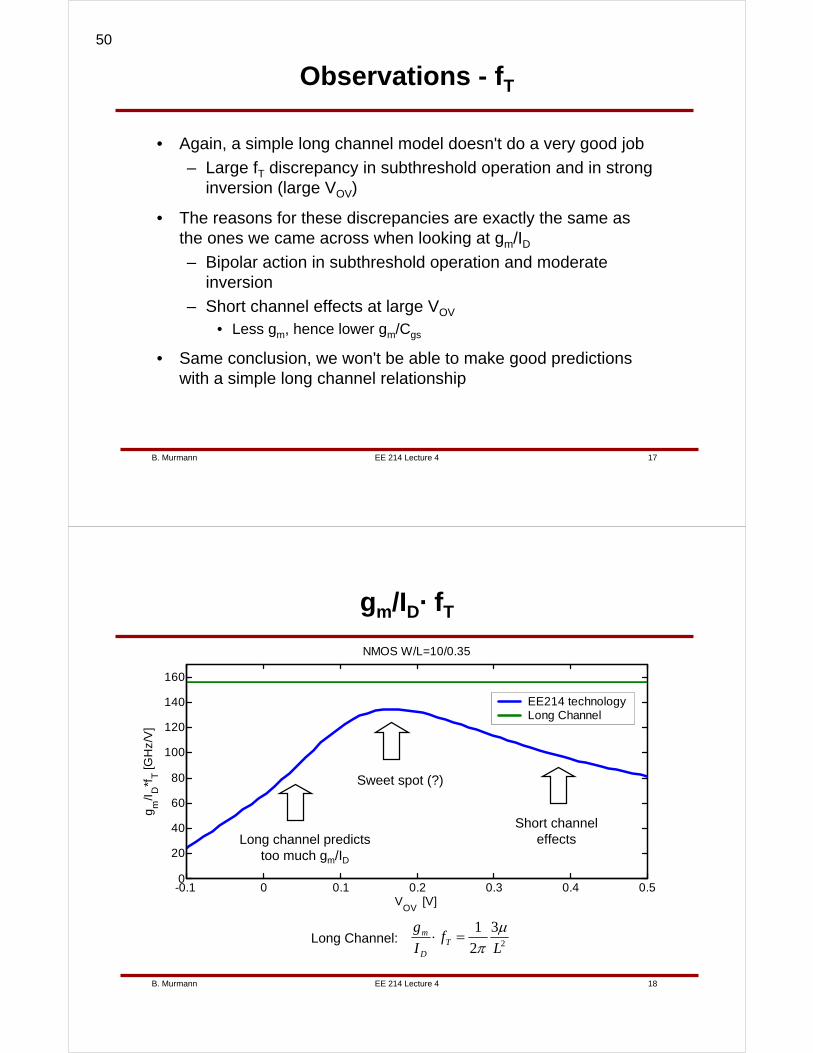
gm/ID· fT
2
3
2
1
Lf
I
gT
D
m μπ
=⋅Long Channel:
-0.1 0 0.1 0.2 0.3 0.4 0.50
20
40
60
80
100
120
140
160
NMOS W/L=10/0.35
VOV
[V]
gm
/ID
*fT [G
Hz/
V]
EE214 technologyLong Channel
Short channel effects
Sweet spot (?)
Long channel predicts too much gm/ID
50
EE 214 Lecture 4B. Murmann 19
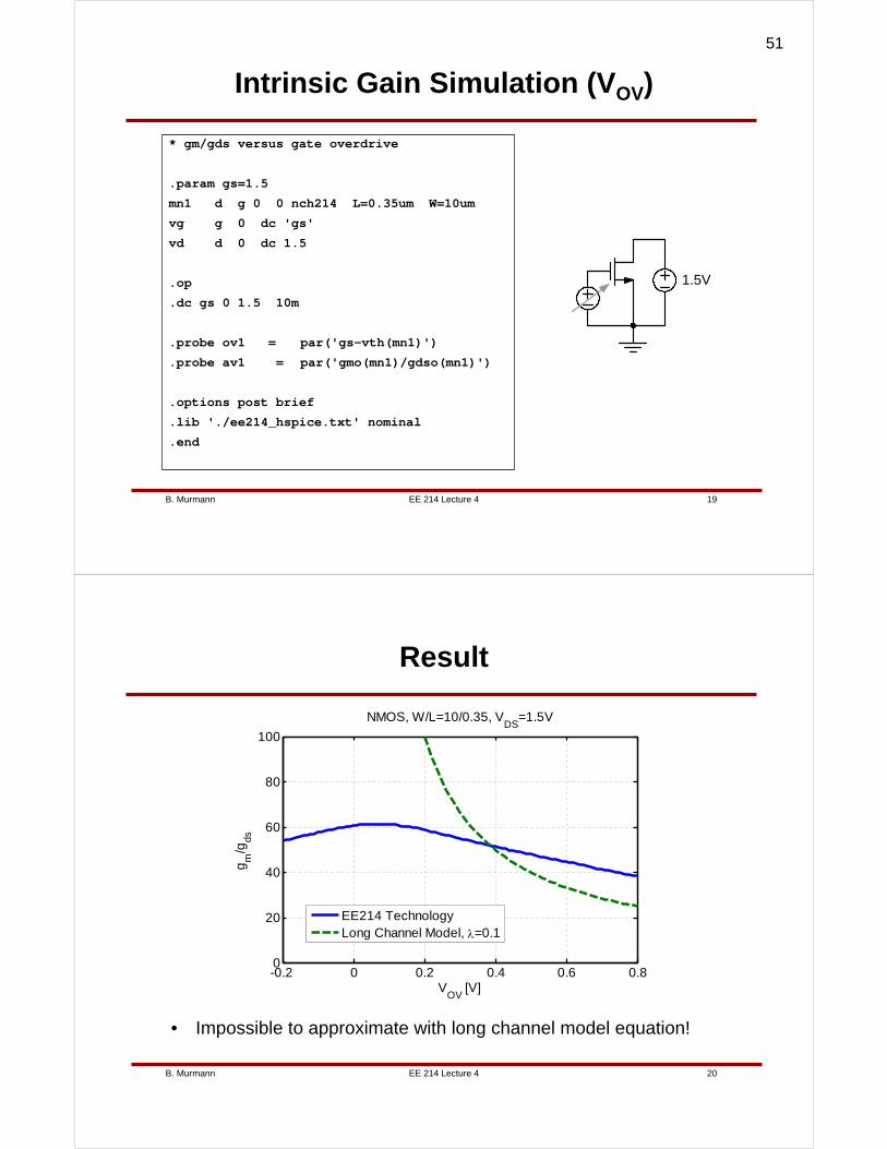
Intrinsic Gain Simulation (VOV)
* gm/gds versus gate overdrive
.param gs=1.5
mn1 d g 0 0 nch214 L=0.35um W=10um
vg g 0 dc 'gs'
vd d 0 dc 1.5
.op
.dc gs 0 1.5 10m
.probe ov1 = par('gs-vth(mn1)')
.probe av1 = par('gmo(mn1)/gdso(mn1)')
.options post brief
.lib './ee214_hspice.txt' nominal
.end
1.5V
EE 214 Lecture 4B. Murmann 20
Result
-0.2 0 0.2 0.4 0.6 0.80
20
40
60
80
100
NMOS, W/L=10/0.35, VDS
=1.5V
VOV
[V]
gm
/gds
EE214 TechnologyLong Channel Model, λ=0.1
• Impossible to approximate with long channel model equation!
51
EE 214 Lecture 4B. Murmann 21
Using a Longer Channel
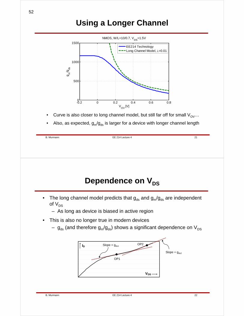
• Curve is also closer to long channel model, but still far off for small VOV…
• Also, as expected, gm/gds is larger for a device with longer channel length
-0.2 0 0.2 0.4 0.6 0.80
500
1000
1500
NMOS, W/L=10/0.7, VDS
=1.5V
VOV
[V]
gm
/gds
EE214 TechnologyLong Channel Model, λ=0.01
EE 214 Lecture 4B. Murmann 22
Dependence on VDS
• The long channel model predicts that gds and gm/gds are independent of VDS
– As long as device is biased in active region
• This is also no longer true in modern devices
– gds (and therefore gm/gds) shows a significant dependence on VDS
VDS
ID
OP1
Slope = gds1OP2
Slope = gds2
52
EE 214 Lecture 4B. Murmann 23
Intrinsic Gain Simulation (VDS)
* gm/gds versus vds
.param vt1=571.5m
mn1 d g 0 0 nch214 L=0.35um W=10um
vg g 0 dc 'vt1+0.2' vd d 0 dc 1.5
.op
.dc vd 0 3 10m
.probe gm1 = par('gmo(mn1)')
.probe gds1 = par('gdso(mn1)')
.options post brief
.lib './ee214_hspice.txt' nominal
.end
EE 214 Lecture 4B. Murmann 24
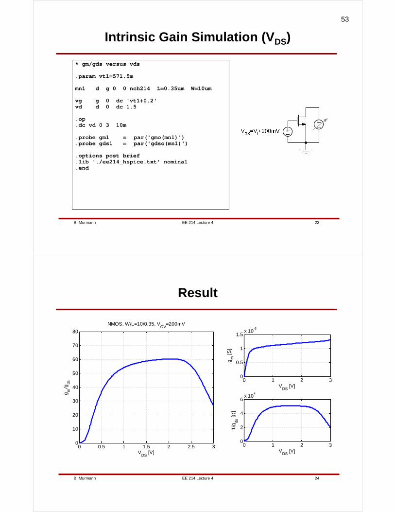
Result
0 1 2 30
0.5
1
1.5x 10
-3
VDS
[V]
gm
[S]
0 1 2 30
2
4
6x 10
4
VDS
[V]
1/g
ds [ Ω
]
0 0.5 1 1.5 2 2.5 30
10
20
30
40
50
60
70
80
NMOS, W/L=10/0.35, VOV
=200mV
VDS
[V]
gm
/gds
53
EE 214 Lecture 4B. Murmann 25
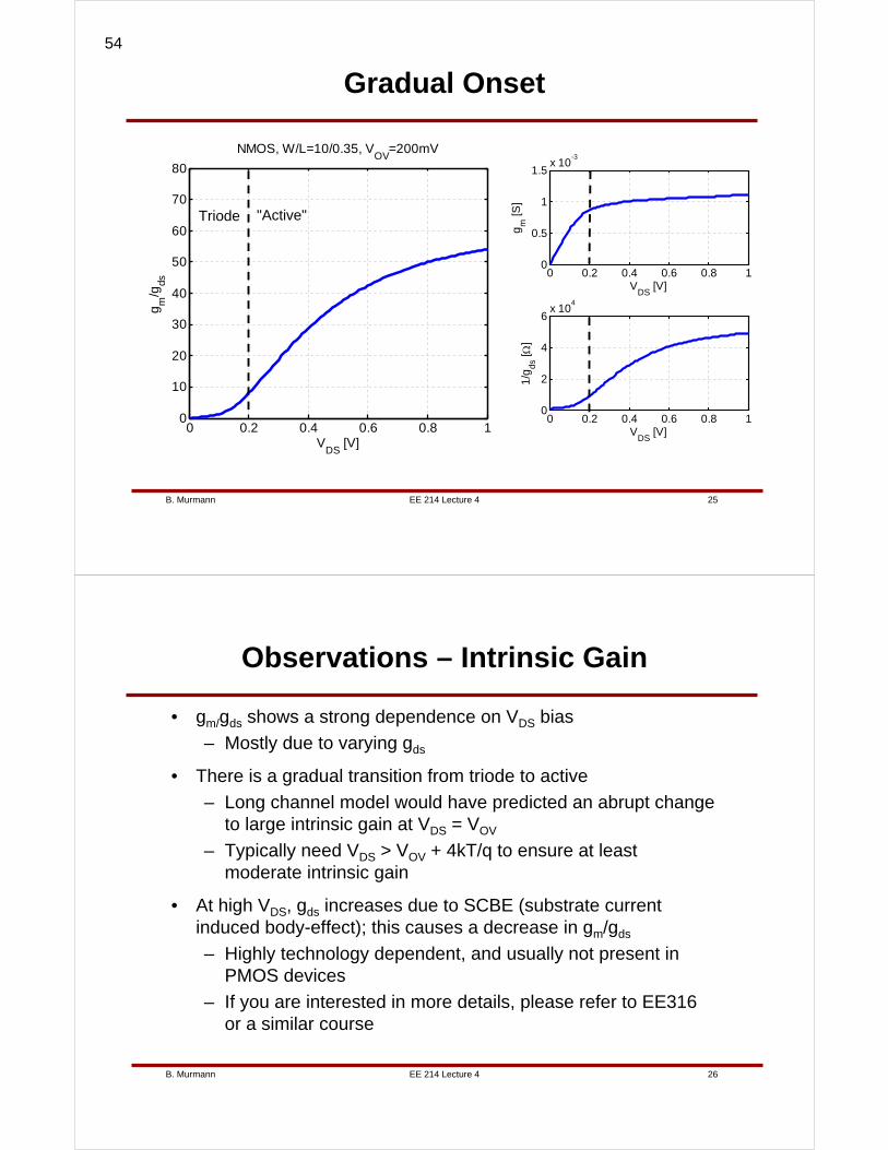
0 0.2 0.4 0.6 0.8 10
10
20
30
40
50
60
70
80
NMOS, W/L=10/0.35, VOV
=200mV
VDS
[V]
gm
/gds
Gradual Onset
Triode
0 0.2 0.4 0.6 0.8 10
0.5
1
1.5x 10
-3
VDS
[V]
gm
[S]
0 0.2 0.4 0.6 0.8 10
2
4
6x 10
4
VDS
[V]
1/g
ds [ Ω
]
"Active"
EE 214 Lecture 4B. Murmann 26
Observations – Intrinsic Gain
• gm/gds shows a strong dependence on VDS bias
– Mostly due to varying gds
• There is a gradual transition from triode to active
– Long channel model would have predicted an abrupt change to large intrinsic gain at VDS = VOV
– Typically need VDS > VOV + 4kT/q to ensure at least moderate intrinsic gain
• At high VDS, gds increases due to SCBE (substrate current induced body-effect); this causes a decrease in gm/gds
– Highly technology dependent, and usually not present in PMOS devices
– If you are interested in more details, please refer to EE316 or a similar course
54
EE 214 Lecture 4B. Murmann 27
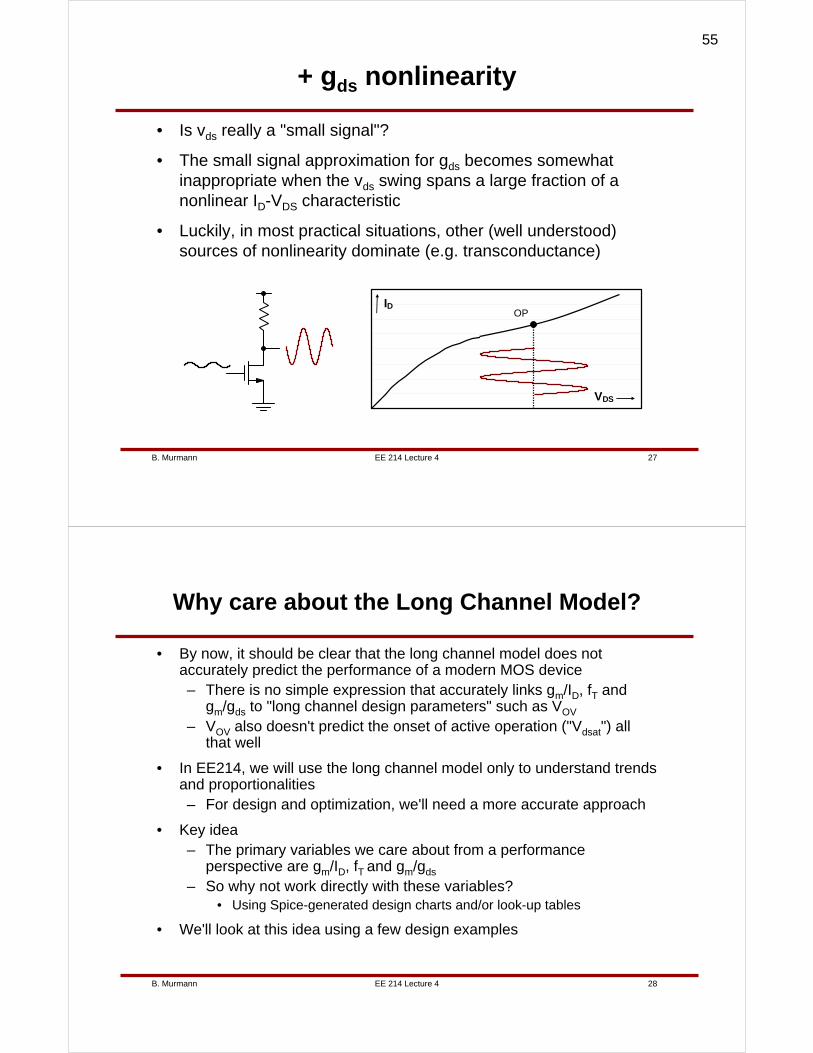
+ gds nonlinearity
• Is vds really a "small signal"?
• The small signal approximation for gds becomes somewhat inappropriate when the vds swing spans a large fraction of a nonlinear ID-VDS characteristic
• Luckily, in most practical situations, other (well understood) sources of nonlinearity dominate (e.g. transconductance)
OP1
VDS
IDOP
EE 214 Lecture 4B. Murmann 28
Why care about the Long Channel Model?
• By now, it should be clear that the long channel model does not accurately predict the performance of a modern MOS device– There is no simple expression that accurately links gm/ID, fT and
gm/gds to "long channel design parameters" such as VOV
– VOV also doesn't predict the onset of active operation ("Vdsat") all that well
• In EE214, we will use the long channel model only to understand trends and proportionalities– For design and optimization, we'll need a more accurate approach
• Key idea– The primary variables we care about from a performance
perspective are gm/ID, fT and gm/gds
– So why not work directly with these variables?• Using Spice-generated design charts and/or look-up tables
• We'll look at this idea using a few design examples
55
EE 214 Lecture 5B. Murmann 1
Lecture 5gm/ID-Based Design
Boris MurmannStanford University
Copyright © 2007 by Boris Murmann
EE 214 Lecture 5B. Murmann 2
Overview
• Introduction
– In the past two lectures, we have learned that the long channel model does not accurately predict the performance of modern MOS devices. Hence, we switch toward a strategy in which circuit-oriented performance metrics (such as gm/ID) are used directly for design and optimization. For a chosen operating point (gm/ID), other relevant parameters (such as the device width) are determined using Spice-generated design charts that serve as a replacement for (inaccurate) model equations.
56
EE 214 Lecture 5B. Murmann 3
Overview
• References– F. Silveira et. al. "A gm/ID based methodology for the design
of CMOS analog circuits and its application to the synthesis of a silicon-on-insulator micropower OTA," IEEE Journal of Solid-State Circuits, Sept. 1996, pp. 1314-1319.
– D. Foty, M. Bucher, D. Binkley, "Re-interpreting the MOS transistor via the inversion coefficient and the continuum of gms/Id," Proc. Int. Conf. on Electronics, Circuits and Systems, pp. 1179-1182, Sept. 2002.
– Denis Flandre's Notes: "Méthodologie gm/ID: un chaînon entre l'analyse symbolique et la synthèse de circuits analogiques basse puissance," available athttp://www.comelec.enst.fr/taisa/Presentations/DenisFlandre.pps
– B. E. Boser, "Analog Circuit Design with Submicron Transistors," IEEE SSCS Meeting, Santa Clara Valley, May 19, 2005, http://www.ewh.ieee.org/r6/scv/ssc/May1905.htm
EE 214 Lecture 5B. Murmann 4
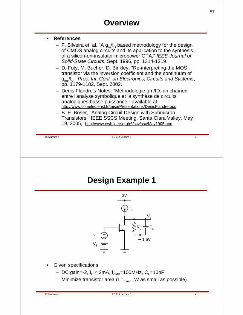
Design Example 1
• Given specifications
– DC gain=-2, IB ≤ 2mA, f-3dB=100MHz, CL=10pF
– Minimize transistor area (L=Lmin, W as small as possible)
Vo
3V
vi
VB
CLRL
1.5V
IB
57

EE 214 Lecture 5B. Murmann 5
Does ro Matter?
• Even at L=Lmin= 0.35μm, we have gmro > 50 (see slide 23 of lecture 4 )
• ro will be negligible in this design problem
( )
omLm
omLmDC
1
oLm
oLmDC
rg
1
Rg
1
2
1
rg
1
Rg
1
A
1
r
1
R
1g
r||RgA
+=
+=
⎟⎟⎠
⎞⎜⎜⎝
⎛+=
=−
EE 214 Lecture 5B. Murmann 6
Hand Calculations (1)
mS6.12159
2g2RgA
159pF10MHz100
1
2
1R
CR
1
2
1f
mLmDC
LLL
dB3
==⇒−=−≅
=⋅
=⇒=−
Ω
Ωππ
• Using all the available current, we have V
.mA
mS.
I
g
D
m 136
2
612==
• How about using less current?
– Using less current means that we'll need a device with larger W
– But specifications asked to minimize W
L
WCI2~g oxDm μ
fixed ↓↓ ↑↑
58
EE 214 Lecture 5B. Murmann 7
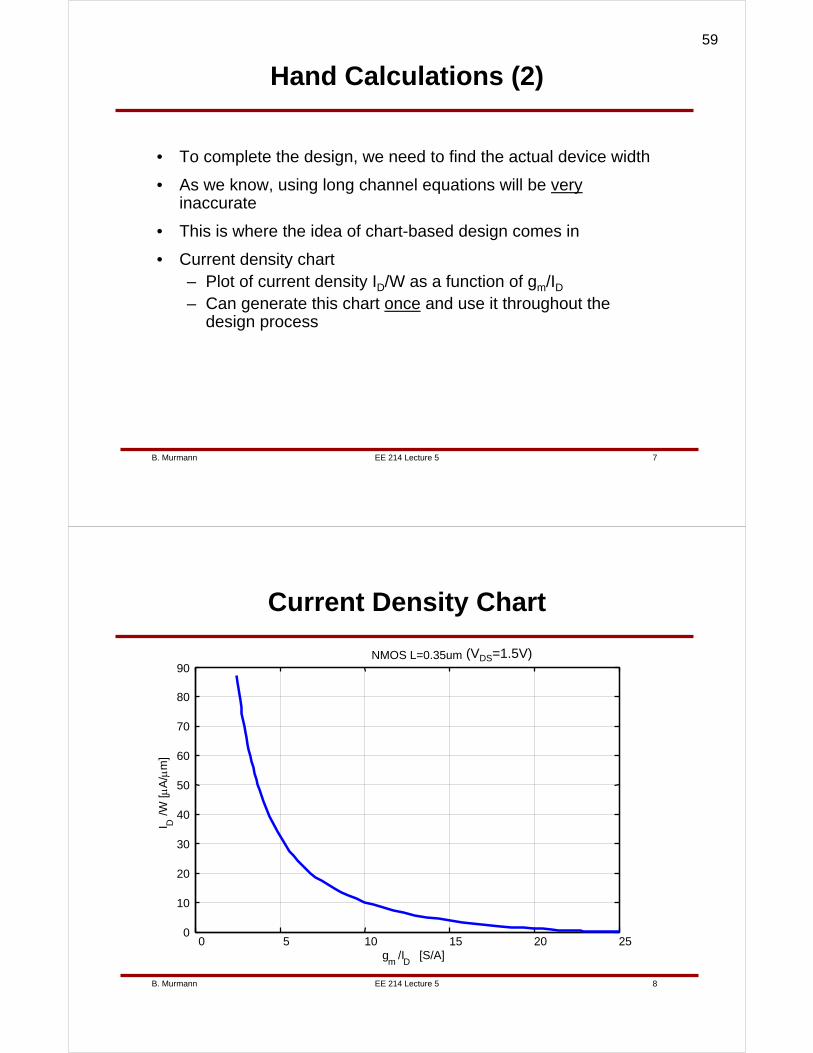
Hand Calculations (2)
• To complete the design, we need to find the actual device width
• As we know, using long channel equations will be veryinaccurate
• This is where the idea of chart-based design comes in
• Current density chart– Plot of current density ID/W as a function of gm/ID– Can generate this chart once and use it throughout the
design process
EE 214 Lecture 5B. Murmann 8
Current Density Chart
(VDS=1.5V)
0 5 10 15 20 250
10
20
30
40
50
60
70
80
90NMOS L=0.35um
gm
/ID
[S/A]
I D/W
[μA
/μm
]
59
EE 214 Lecture 5B. Murmann 9
A Better Current Density Chart
(VDS=1.5V)
3 4 5 6 7 8 9 10 11 12 13 14 15 16 17 18 19 2010
0
101
NMOS L=0.35um
gm
/ID
[S/A]
I D/W
[μA
/μm
]23μA/μm
6.3 1/V
(VDS=1.5V)
EE 214 Lecture 5B. Murmann 10
Spice Verification
• So, the device width is
• How to set VB?– E.g. using a replica
device (MN2)
mm
WI
IWD
D μμ 8723
2000===
Vo
3V
vi
CLRL
1.5V
IBIB
VB
MN1MN2
60
EE 214 Lecture 5B. Murmann 11
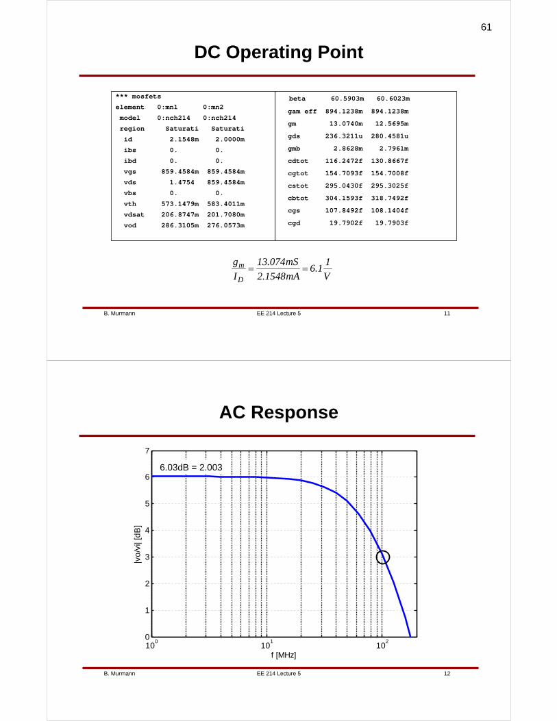
DC Operating Point
*** mosfets
element 0:mn1 0:mn2
model 0:nch214 0:nch214
region Saturati Saturati
id 2.1548m 2.0000m
ibs 0. 0.
ibd 0. 0.
vgs 859.4584m 859.4584m
vds 1.4754 859.4584m
vbs 0. 0.
vth 573.1479m 583.4011m
vdsat 206.8747m 201.7080m
vod 286.3105m 276.0573m
beta 60.5903m 60.6023m
gam eff 894.1238m 894.1238m
gm 13.0740m 12.5695m
gds 236.3211u 280.4581u
gmb 2.8628m 2.7961m
cdtot 116.2472f 130.8667f
cgtot 154.7093f 154.7008f
cstot 295.0430f 295.3025f
cbtot 304.1593f 318.7492f
cgs 107.8492f 108.1404f
cgd 19.7902f 19.7903f
V
11.6
mA1548.2
mS074.13
I
g
D
m ==
EE 214 Lecture 5B. Murmann 12
100
101
102
0
1
2
3
4
5
6
7
f [MHz]
|vo
/vi|
[dB
]
AC Response
6.03dB = 2.003
61
EE 214 Lecture 5B. Murmann 13
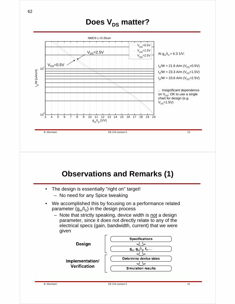
Does VDS matter?
3 4 5 6 7 8 9 10 11 12 13 14 15 16 17 18 19 2010
0
101
NMOS L=0.35um
gm
/ID
[1/V]
I D/W
[uA
/um
]
VDS
=0.5V
VDS
=1.5V
VDS
=2.5VAt gm/ID = 6.3 1/V:
ID/W = 21.8 A/m (VDS=0.5V)
ID/W = 23.3 A/m (VDS=1.5V)
ID/W = 23.6 A/m (VDS=2.5V)
∴ Insignificant dependence on VDS; OK to use a single chart for design (e.g. VDS=1.5V)
VDS=0.5V
VDS=2.5V
EE 214 Lecture 5B. Murmann 14
Observations and Remarks (1)
• The design is essentially "right on" target!– No need for any Spice tweaking
• We accomplished this by focusing on a performance related parameter (gm/ID) in the design process– Note that strictly speaking, device width is not a design
parameter, since it does not directly relate to any of the electrical specs (gain, bandwidth, current) that we were given
62

EE 214 Lecture 5B. Murmann 15
Observations and Remarks (2)
• The key advantage of gm/ID based design is that it allows you to transition from hand analysis to Spice without much of the "usual" modeling uncertainties
– Simply because we are incorporating relevant simulation data into the design process
– Enables you to optimize your circuit without even running a Spice simulation
• To see why this is good, let's compare with some popular alternatives, as seen in many labs and cubicles around the country…
EE 214 Lecture 5B. Murmann 16
Design Methodology 1 (Worst)
• Have an existing design that somehow works for a different process, different specs, …
• Port this design over and tweak all 137 transistor geometries until I meet the specs…
• 500 Spice runs later, I am approaching the deadline with a design that somehow works, god knows how/why
63

EE 214 Lecture 5B. Murmann 17
Design Methodology 2 (Better)
• Remember the square law transistor model from class
• Go through the pain of estimating μCox, and do some hand calculations
• Plug my design into Spice and realize that everything is about 20…80% off
• Throw away my hand analysis and revert back to the "Spice Monkey" design flow from here
EE 214 Lecture 5B. Murmann 18
Design Methodology 3 (Much Better)
• Spend some time to characterize your technology using Spice
– E.g. intrinsic gain and current density as a function of gm/ID
• Do hand calculations using the generated technology data
– Use Matlab, MathCAD or Excel script
– Quickly iterate through tens of different designs, if necessary
• Implement and verify in Spice
– Only minor tweaking necessary (if any)
– Done!
64
EE 214 Lecture 5B. Murmann 19
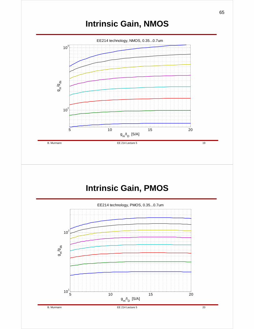
Intrinsic Gain, NMOS
5 10 15 20
102
103
EE214 technology, NMOS, 0.35...0.7um
gm
/ID
[S/A]
gm
/gds
EE 214 Lecture 5B. Murmann 20
Intrinsic Gain, PMOS
5 10 15 2010
1
102
EE214 technology, PMOS, 0.35...0.7um
gm
/ID
[S/A]
gm
/gds
65
EE 214 Lecture 5B. Murmann 21
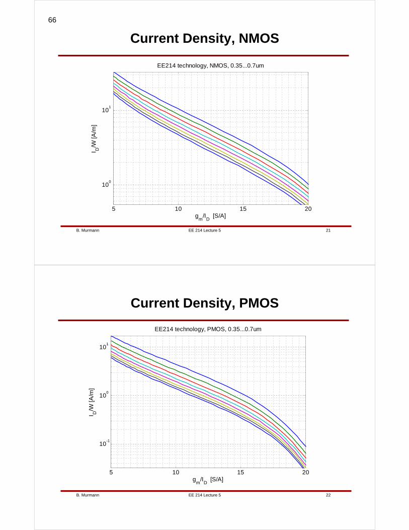
Current Density, NMOS
5 10 15 20
100
101
EE214 technology, NMOS, 0.35...0.7um
gm
/ID
[S/A]
I D/W
[A/m
]
EE 214 Lecture 5B. Murmann 22
Current Density, PMOS
5 10 15 20
10-1
100
101
EE214 technology, PMOS, 0.35...0.7um
gm
/ID
[S/A]
I D/W
[A/m
]
66

EE 214 Lecture 5B. Murmann 23
+ A Note on Current Density Charts
• Designing with current density charts in a normalized, width-independent space works because
– Current density and gm/ID are independent of W• ID/W ~ W/W
• gm/ID ~ W/W
– There is a one-to-one mapping from gm/ID to current density
( ) ( ) ⎟⎟⎠
⎞⎜⎜⎝
⎛⎟⎟⎠
⎞⎜⎜⎝
⎛===
⎟⎟⎠
⎞⎜⎜⎝
⎛===
−
−
D
m1OV
DOV
D
m
2
m
Dox
2OVox
D
OVD
m
I
gfgVg
W
IVf
I
g
g
I2
L
1CV
L
1C
2
1
W
I
V
2
I
g μμLong channel:
General case:
67
EE 214 Lecture 6B. Murmann 1
Lecture 6Extrinsic Capacitance
Boris MurmannStanford University
Copyright © 2007 by Boris Murmann
EE 214 Lecture 6B. Murmann 2
Overview
• Reading
– 1.6.7 (Parasitic Elements)
• Introduction
– In today's lecture, we'll look at another CS amplifier design example – this time with an input source that has a relatively large resistance. Through this example, we find that we need more modeling to accurately predict the resulting pole at the gate node. Our discussion leads to a discussion of parasitic extrinsic capacitors around the MOSFET - overlap and junction capacitance.
68

EE 214 Lecture 6B. Murmann 3
Design Example 2
• Given specifications
– DC gain=-4, IB ≤ 0.5mA
– RL=1k, Ri=10k
– Maximize and estimate bandwidth
Vo
VDD
vi
VB
roCgsgmvgs
+vgs-
+vo-
RL
Ri
Transducer Rivi
RL
1.5V
IB
gsiLom
i
o
CsR1
1)R||r(g
)s(v
)s(v)s(H
+⋅−==
DC gain FrequencyDependence
EE 214 Lecture 6B. Murmann 4
Hand Calculation
• Just as in the previous design example, we know thatgm/gds >> |ADC|. Hence we simply find
mS4k1
4g
4RgA
m
LmDC
==
−=−≅
Ω
• In order to maximize bandwidth, we need to make Cgs (and hence W) as small as possible. Again, this is the case for usingup all the available current
VmA.
mS
I
g
D
m 18
50
4==
• In order to estimate the circuit's bandwidth, we need to know Cgs
– Solution: transit frequency chart
69
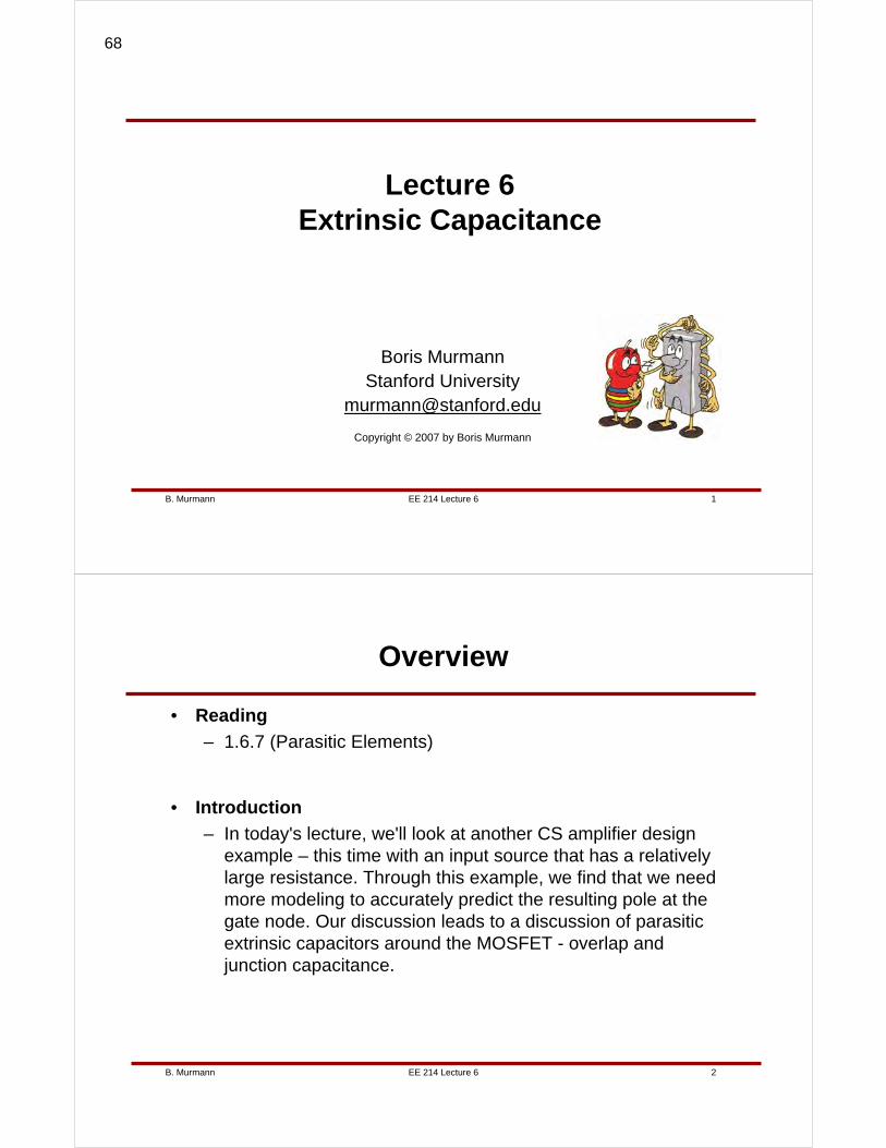
EE 214 Lecture 6B. Murmann 5
Transit Frequency Chart
0 5 10 15 20 250
5
10
15
20
25
30NMOS L=0.35um
gm
/ID
[1/V]
f T [G
Hz] 16GHz
EE 214 Lecture 6B. Murmann 6
Bandwidth
• Using the transit frequency chart, we find
fFGHz
mS
f
gC
T
mgs 40
16
4
2
1
2
1===
ππ
MHzfFkCR
fgsi
dB 3984010
1
2
11
2
13 =
⋅==− ππ
• As a last step, we use the current density chart to find the device width
70
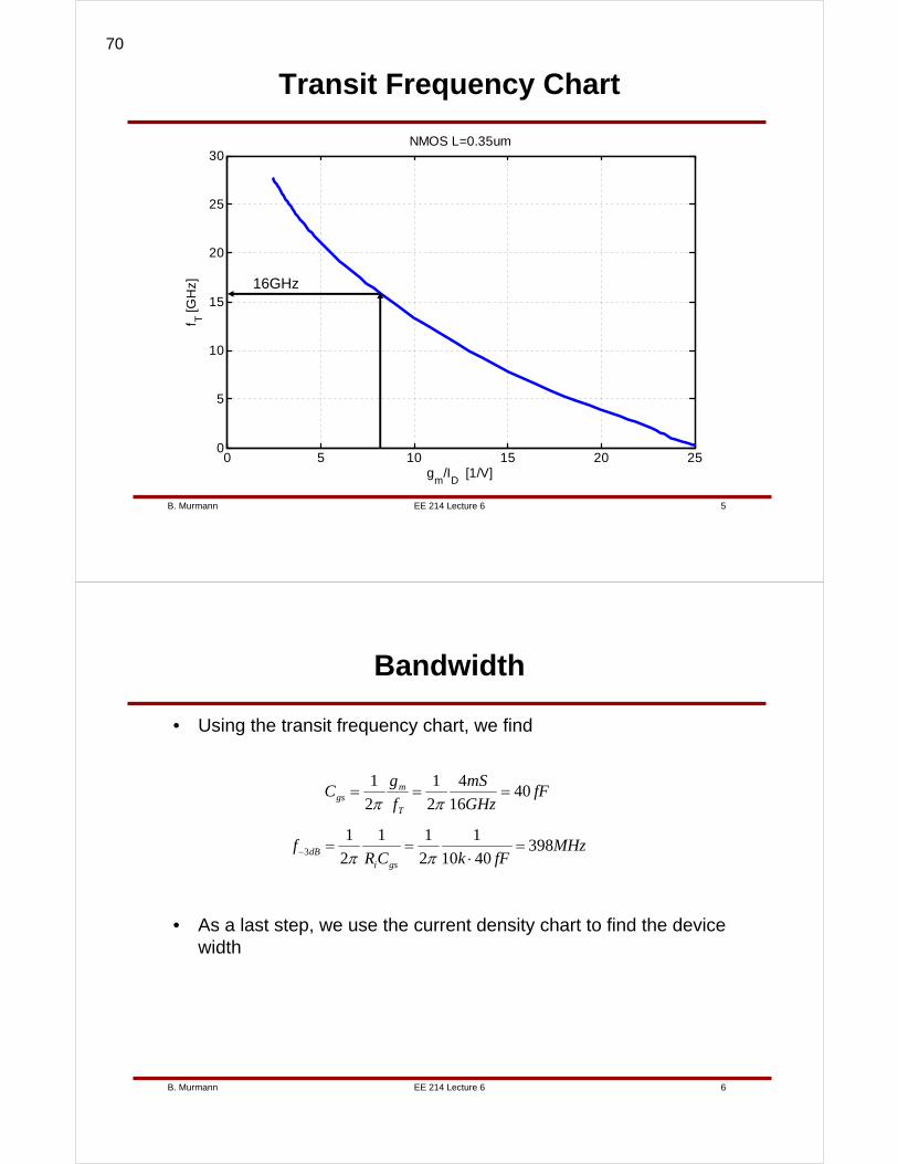
EE 214 Lecture 6B. Murmann 7
3 4 5 6 7 8 9 10 11 12 13 14 15 16 17 18 19 2010
0
101
NMOS L=0.35um
gm
/ID
[1/V]
I D/W
[uA
/um
]
Current Density Chart
15.5μA/μm
EE 214 Lecture 6B. Murmann 8
Spice Verification
• Device width
• Simulation circuit
m.
WI
IWD
D μ32515
500===
71
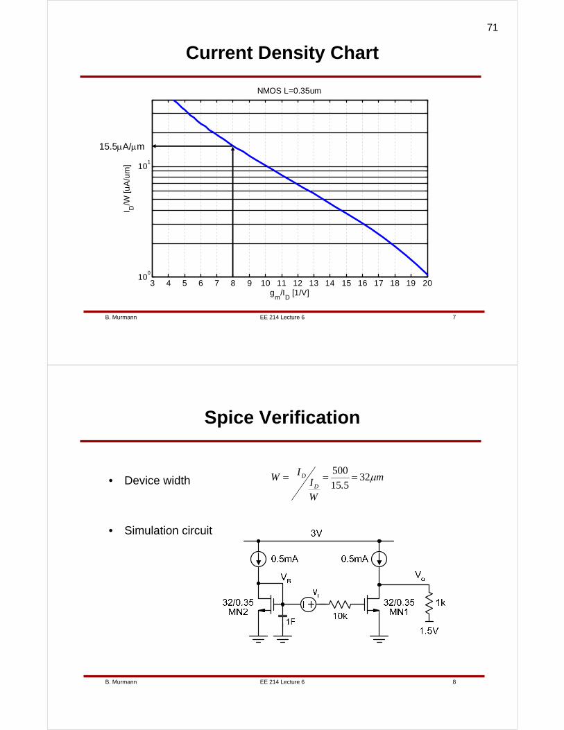
EE 214 Lecture 6B. Murmann 9
DC Operating Point
**** mosfets
element 0:mn2 0:mn1
model 0:nch214 0:nch214
region Saturati Saturati
id 500.0000u 549.5104u
ibs 0. 0.
ibd 0. 0.
vgs 806.0164m 806.0164m
vds 806.0164m 1.4505
vbs 0. 0.
vth 584.0239m 573.2955m
vdsat 172.3376m 178.0416m
vod 221.9925m 232.7209m
beta 22.1486m 22.1424m
gam eff 894.1238m 894.1238m
gm 3.9889m 4.2006m
gds 84.1846u 73.4138u
gmb 894.3095u 927.0356u
cdtot 49.1459f 43.2542f
cgtot 56.5600f 56.5745f
cstot 108.9160f 108.8336f
cbtot 118.8806f 113.0007f
cgs 39.4669f 39.3691f
cgd 7.2418f 7.2416f
A
S65.7
A549
mS2.4
I
g
D
m ==μ
fF4.39Cgs = Good agreement.
EE 214 Lecture 6B. Murmann 10
100
101
102
103
0
5
10
15
f [MHz]
|vo
/vi|
[dB
]
Frequency Response
• Simulation result: f-3dB=184MHz; hand analysis: f-3dB=398MHz (!)
3dB
11.85dB = 3.91
72
EE 214 Lecture 6B. Murmann 11
Interpretation
• Even though the estimated value of Cgs matches simulation data very well, there is a large error in the estimated bandwidth
– Means that our simple bandwidth expression is quite inaccurate
• The reason for this discrepancy is that we have neglected "extrinsic" capacitances that affect the frequency response of our circuit in a significant way
• This example motivates the need for a more accurate capacitance model
EE 214 Lecture 6B. Murmann 12
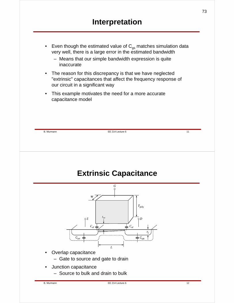
Extrinsic Capacitance
• Overlap capacitance– Gate to source and gate to drain
• Junction capacitance– Source to bulk and drain to bulk
CjdbCjsb
73
EE 214 Lecture 6B. Murmann 13
Overlap Capacitance
• Two components
– Direct overlap ~ CoxWLoverlap
– Additional component due to fringing field• Non-negligible in modern technology (gate thickness is large
compared to other feature sizes)
• EE214 technology parameters (capacitance per width)
– NMOS: Col= 0.23fF/μm
– PMOS: Col= 0.48fF/μm
EE 214 Lecture 6B. Murmann 14
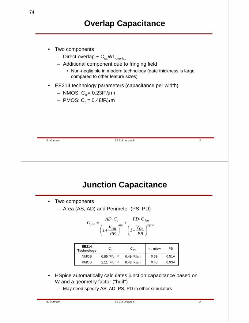
Junction Capacitance
• Two components
– Area (AS, AD) and Perimeter (PS, PD)
mjswDB
jswmj
DB
jjdb
PBV
1
CPD
PBV
1
CADC
⎟⎠⎞
⎜⎝⎛ +
⋅+
⎟⎠⎞
⎜⎝⎛ +
⋅=
0.93V0.480.48 fF/μm1.11 fF/μm2PMOS
0.51V0.390.49 fF/μm0.85 fF/μm2NMOS
PBmj, mjswCjswCjEE214
Technology
• HSpice automatically calculates junction capacitance based on W and a geometry factor ("hdif")– May need specify AS, AD, PS, PD in other simulators
74
EE 214 Lecture 6B. Murmann 15
Layout Dependence (hdif=0.5μm)
Wm2PD
W2m4PS2
Wm1AD
Wm1AS
+=+=
⋅=
⋅=
μμ
μ
μ
W2m2PDPS
Wm1ADAS
+==⋅==
μμ
(1μm=2*hdif)
EE 214 Lecture 6B. Murmann 16
MOS Capacitor Summary
"small""small"Cgb
Cjsb+ 2/3CCBCjsb+ CCB/2CjsbCsb
CjdbCjdb+ CCB/2CjdbCdb
Col½ WLCox+ColColCgd
2/3 WLCox + Col½ WLCox+ ColColCgs
ActiveTriodeSubthreshold
111
−
⎟⎟⎠
⎞⎜⎜⎝
⎛+
oxCB WLCC
75
EE 214 Lecture 6B. Murmann 17
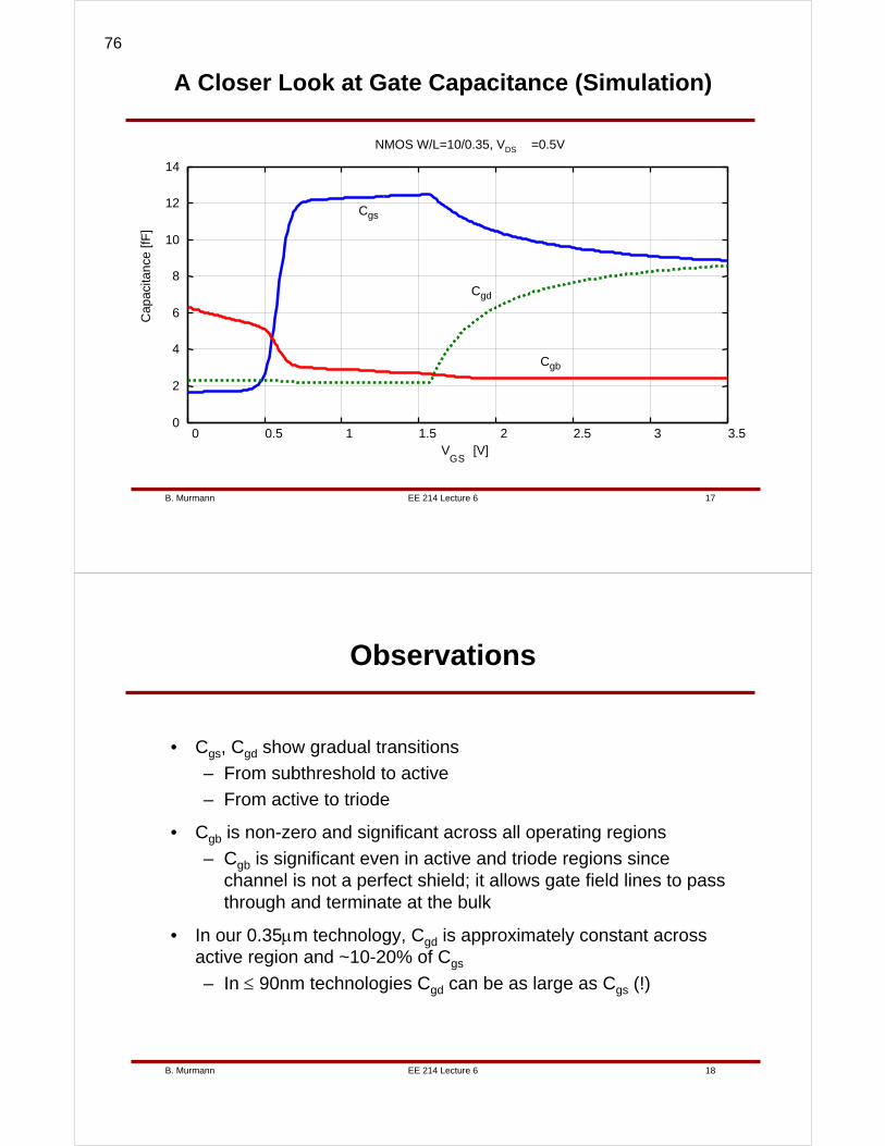
A Closer Look at Gate Capacitance (Simulation)
0 0.5 1 1.5 2 2.5 3 3.50
2
4
6
8
10
12
14
NMOS W/L=10/0.35, VDS =0.5V
VGS
[V]
Cap
acita
nce
[fF]
Cgs
Cgd
Cgb
EE 214 Lecture 6B. Murmann 18
Observations
• Cgs, Cgd show gradual transitions
– From subthreshold to active
– From active to triode
• Cgb is non-zero and significant across all operating regions
– Cgb is significant even in active and triode regions since channel is not a perfect shield; it allows gate field lines to pass through and terminate at the bulk
• In our 0.35μm technology, Cgd is approximately constant across active region and ~10-20% of Cgs
– In ≤ 90nm technologies Cgd can be as large as Cgs (!)
76
EE 214 Lecture 6B. Murmann 19
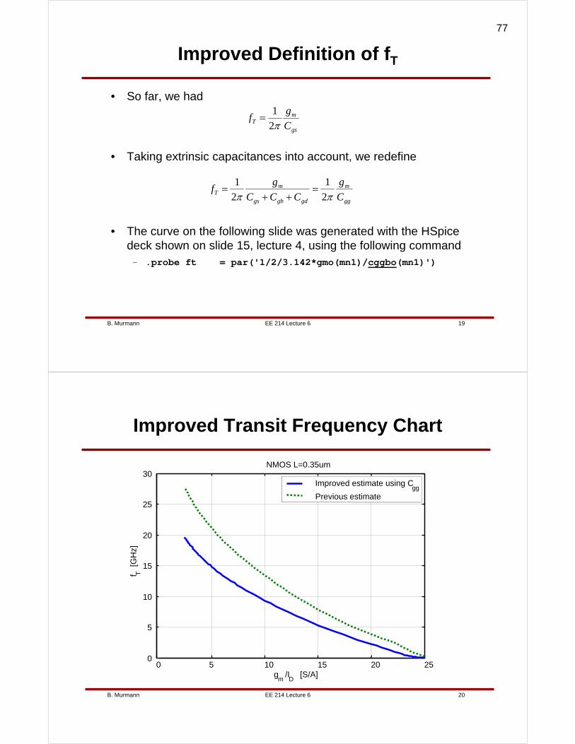
Improved Definition of fT
• So far, we had
gs
mT C
gf
π21
=
• Taking extrinsic capacitances into account, we redefine
gg
m
gdgbgs
mT C
g
CCC
gf
ππ 2
1
2
1=
++=
• The curve on the following slide was generated with the HSpice deck shown on slide 15, lecture 4, using the following command – .probe ft = par('1/2/3.142*gmo(mn1)/cggbo(mn1)')
EE 214 Lecture 6B. Murmann 20
Improved Transit Frequency Chart
11.25
0 5 10 15 20 250
5
10
15
20
25
30NMOS L=0.35um
gm
/ID
[S/A]
f T[G
Hz]
Improved estimate using Cgg
Previous estimate
77
EE 214 Lecture 6B. Murmann 21
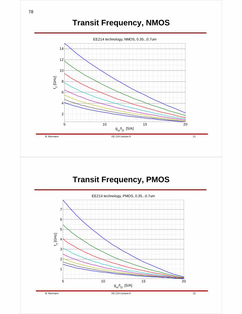
Transit Frequency, NMOS
5 10 15 20
2
4
6
8
10
12
14
EE214 technology, NMOS, 0.35...0.7um
gm
/ID
[S/A]
f T [G
Hz]
EE 214 Lecture 6B. Murmann 22
Transit Frequency, PMOS
5 10 15 20
1
2
3
4
5
6
7
EE214 technology, PMOS, 0.35...0.7um
gm
/ID
[S/A]
f T [G
Hz]
78
EE 214 Lecture 6B. Murmann 23
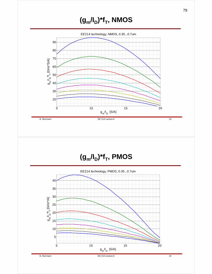
(gm/ID)*fT, NMOS
5 10 15 20
20
30
40
50
60
70
80
90
EE214 technology, NMOS, 0.35...0.7um
gm
/ID
[S/A]
gm
/ID
*fT [G
Hz*
S/A
]
EE 214 Lecture 6B. Murmann 24
(gm/ID)*fT, PMOS
5 10 15 20
5
10
15
20
25
30
35
40
EE214 technology, PMOS, 0.35...0.7um
gm
/ID
[S/A]
gm
/ID
*fT [G
Hz*
/A]
79
EE 214 Lecture 6B. Murmann 25
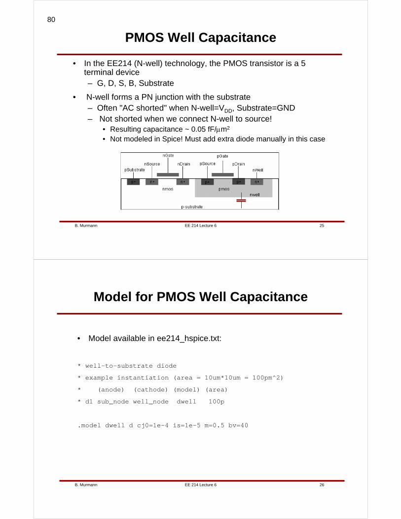
PMOS Well Capacitance
• In the EE214 (N-well) technology, the PMOS transistor is a 5 terminal device– G, D, S, B, Substrate
• N-well forms a PN junction with the substrate– Often "AC shorted" when N-well=VDD, Substrate=GND– Not shorted when we connect N-well to source!
• Resulting capacitance ~ 0.05 fF/μm2
• Not modeled in Spice! Must add extra diode manually in this case
EE 214 Lecture 6B. Murmann 26
Model for PMOS Well Capacitance
• Model available in ee214_hspice.txt:
* well-to-substrate diode
* example instantiation (area = 10um*10um = 100pm^2)
* (anode) (cathode) (model) (area)
* d1 sub_node well_node dwell 100p
.model dwell d cj0=1e-4 is=1e-5 m=0.5 bv=40
80
EE 214 Lecture 6B. Murmann 27
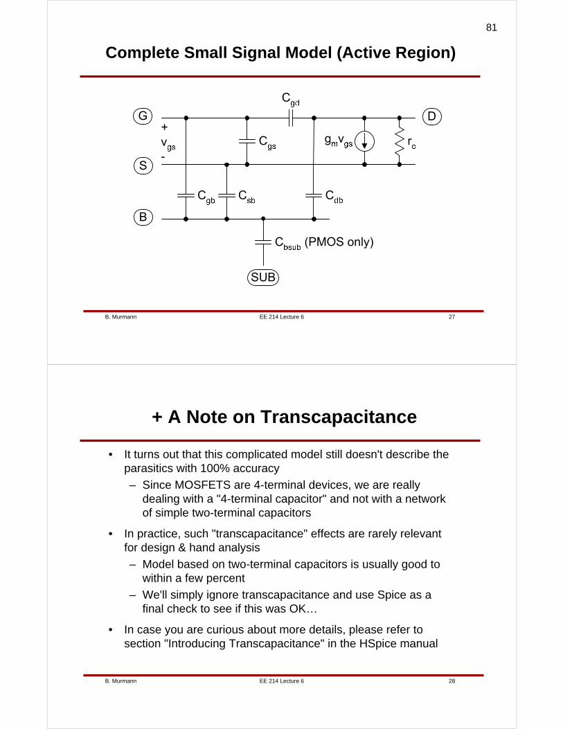
Complete Small Signal Model (Active Region)
EE 214 Lecture 6B. Murmann 28
+ A Note on Transcapacitance
• It turns out that this complicated model still doesn't describe the parasitics with 100% accuracy
– Since MOSFETS are 4-terminal devices, we are really dealing with a "4-terminal capacitor" and not with a network of simple two-terminal capacitors
• In practice, such "transcapacitance" effects are rarely relevantfor design & hand analysis
– Model based on two-terminal capacitors is usually good to within a few percent
– We'll simply ignore transcapacitance and use Spice as a final check to see if this was OK…
• In case you are curious about more details, please refer to section "Introducing Transcapacitance" in the HSpice manual
81
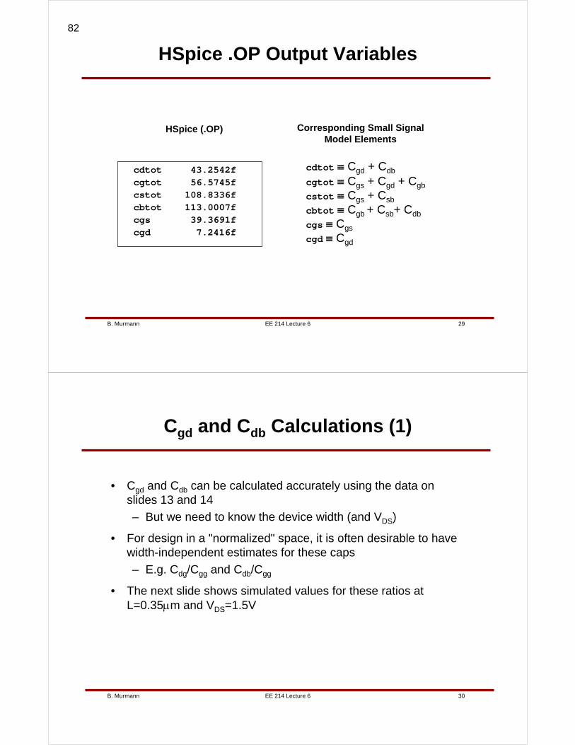
EE 214 Lecture 6B. Murmann 29
HSpice .OP Output Variables
cdtot 43.2542fcgtot 56.5745fcstot 108.8336fcbtot 113.0007fcgs 39.3691fcgd 7.2416f
cdtot ≡ Cgd + Cdb
cgtot ≡ Cgs + Cgd + Cgb
cstot ≡ Cgs + Csb
cbtot ≡ Cgb + Csb+ Cdb
cgs ≡ Cgs
cgd ≡ Cgd
HSpice (.OP) Corresponding Small SignalModel Elements
EE 214 Lecture 6B. Murmann 30
Cgd and Cdb Calculations (1)
• Cgd and Cdb can be calculated accurately using the data on slides 13 and 14
– But we need to know the device width (and VDS)
• For design in a "normalized" space, it is often desirable to have width-independent estimates for these caps
– E.g. Cdg/Cgg and Cdb/Cgg
• The next slide shows simulated values for these ratios at L=0.35μm and VDS=1.5V
82
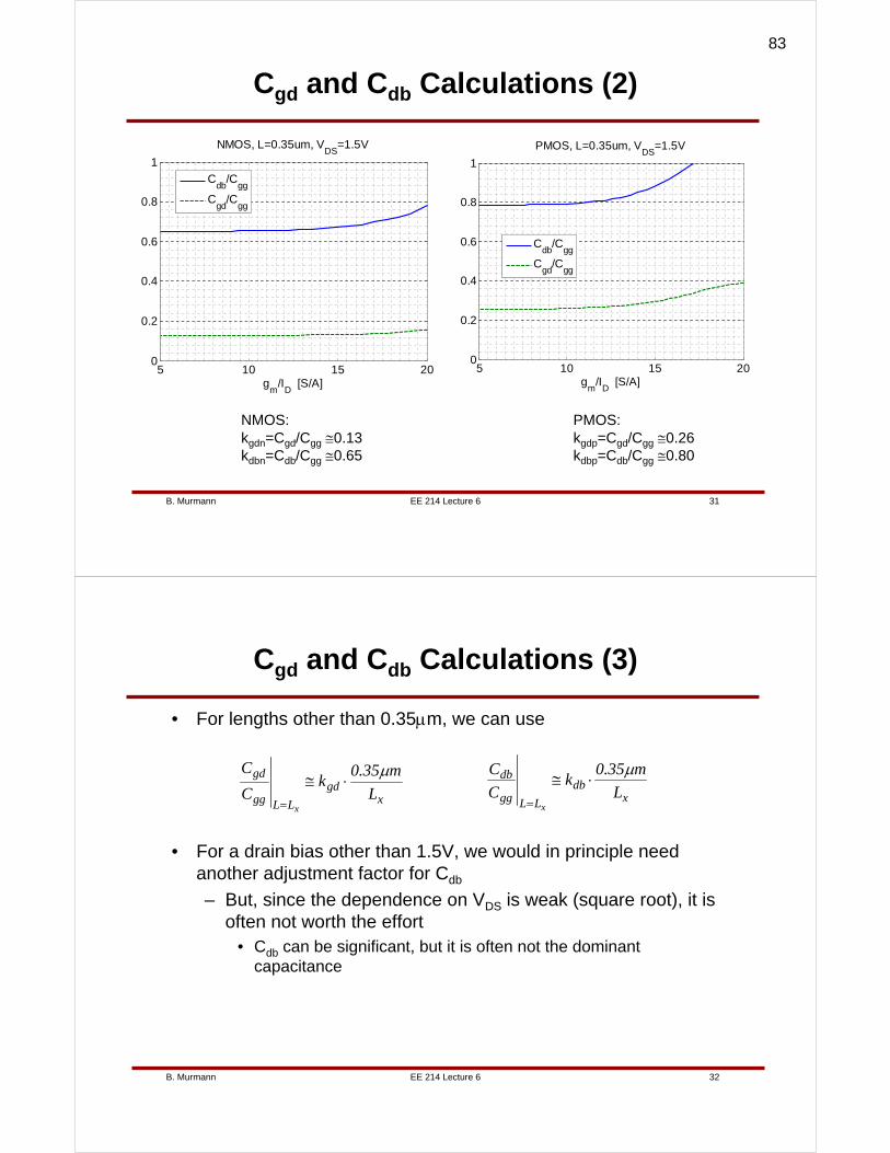
EE 214 Lecture 6B. Murmann 31
Cgd and Cdb Calculations (2)
5 10 15 200
0.2
0.4
0.6
0.8
1
NMOS, L=0.35um, VDS
=1.5V
gm
/ID
[S/A]
Cdb
/Cgg
Cgd
/Cgg
5 10 15 200
0.2
0.4
0.6
0.8
1
PMOS, L=0.35um, VDS
=1.5V
gm
/ID
[S/A]
Cdb
/Cgg
Cgd
/Cgg
NMOS:kgdn=Cgd/Cgg ≅0.13kdbn=Cdb/Cgg ≅0.65
PMOS:kgdp=Cgd/Cgg ≅0.26kdbp=Cdb/Cgg ≅0.80
EE 214 Lecture 6B. Murmann 32
Cgd and Cdb Calculations (3)
• For lengths other than 0.35μm, we can use
xdb
LLgg
db
L
m35.0k
C
C
x
μ⋅≅
=xgd
LLgg
gd
L
m35.0k
C
C
x
μ⋅≅
=
• For a drain bias other than 1.5V, we would in principle need another adjustment factor for Cdb
– But, since the dependence on VDS is weak (square root), it is often not worth the effort
• Cdb can be significant, but it is often not the dominant capacitance
83
EE 214 Lecture 6B. Murmann 33
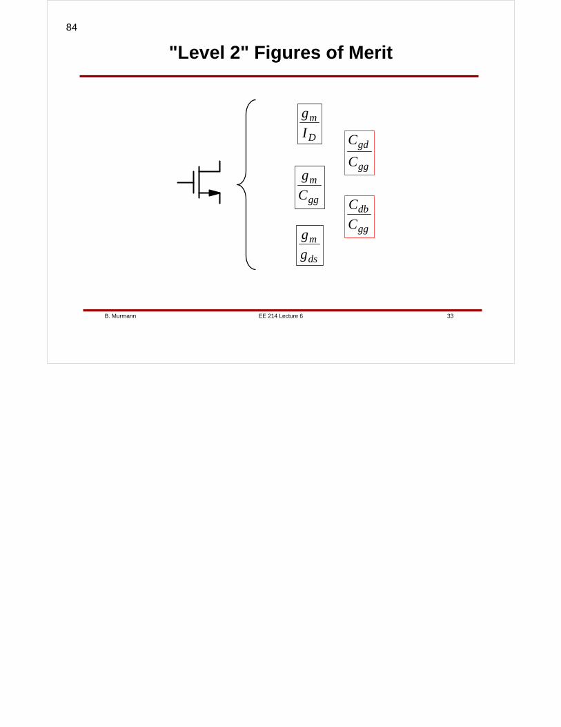
"Level 2" Figures of Merit
D
m
I
g
gg
m
C
g
ds
m
g
g
gg
gd
C
C
gg
db
C
C
84
EE 214 Lecture 7B. Murmann 1
Lecture 7Miller Approximation
Zero-Value Time Constant Analysis
Boris MurmannStanford University
Copyright © 2007 by Boris Murmann
EE 214 Lecture 7B. Murmann 2
Overview
• Reading– 7.1, 7.2.0, 7.2.1 (Miller Effect in CS Stage, only pp. 488-493)– 7.3.0, 7.3.1 7.3.2 (Zero-Value Time Constant Analysis)– 7.3.3 (Cascade Amplifier Frequency Response) – Supplementary document "Bandwidth estimation techniques," by
Tom Lee (optional, see website).
• Introduction– Last lecture, we found that using a simple circuit model based on
intrinsic capacitance only is not sufficient for accurate bandwidth prediction in our CS stage. Having learned about the involved extrinsic capacitances, we are now in a position to improve our hand analysis and match the Spice result with good precision. Tosimplify the analysis, we will utilize the so-called "Miller Approximation." Next, we will take at look at the the "Zero-Value Time Constant Analysis" as an alternative method, which is useful for a much broader class of circuits.
85
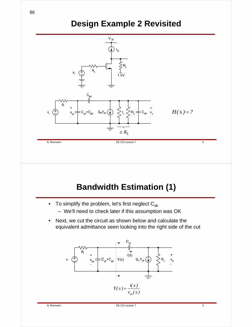
EE 214 Lecture 7B. Murmann 3
Design Example 2 Revisited
?)s(H =
LR≅
EE 214 Lecture 7B. Murmann 4
Bandwidth Estimation (1)
• To simplify the problem, let's first neglect Cdb
– We'll need to check later if this assumption was OK
• Next, we cut the circuit as shown below and calculate the equivalent admittance seen looking into the right side of the cut
)s(v
)s(i)s(Y
gs
=
86
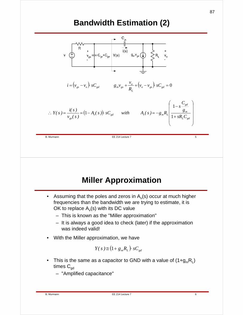
EE 214 Lecture 7B. Murmann 5
Bandwidth Estimation (2)
( ) ( ) 0=⋅−++⋅−= gdgsoL
ogsmgdogs sCvv
R
vvgsCvvi
( )⎟⎟⎟⎟
⎠
⎞
⎜⎜⎜⎜
⎝
⎛
+
−−=⋅−==∴
gdL
m
gd
Lmvgdvgs CsR
g
Cs
Rg)s(AwithsC)s(A)s(v
)s(i)s(Y
1
1
1
EE 214 Lecture 7B. Murmann 6
Miller Approximation
• Assuming that the poles and zeros in Av(s) occur at much higher frequencies than the bandwidth we are trying to estimate, it is OK to replace Av(s) with its DC value
– This is known as the "Miller approximation"
– It is always a good idea to check (later) if the approximation was indeed valid!
• With the Miller approximation, we have
( ) gdLm sCRg)s(Y ⋅+≅ 1
• This is the same as a capacitor to GND with a value of (1+gmRL) times Cgd
– "Amplified capacitance"
87
EE 214 Lecture 7B. Murmann 7
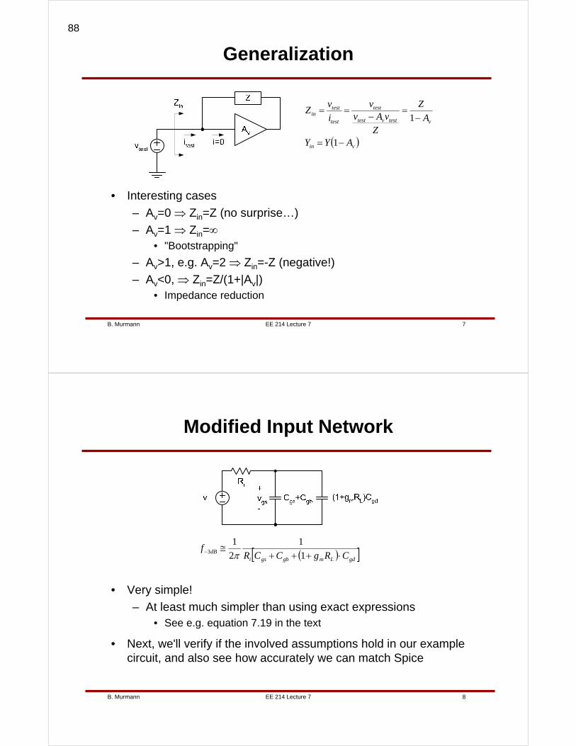
Generalization
• Interesting cases
– Av=0 ⇒ Zin=Z (no surprise…)
– Av=1 ⇒ Zin=∞• "Bootstrapping"
– Av>1, e.g. Av=2 ⇒ Zin=-Z (negative!)
– Av<0, ⇒ Zin=Z/(1+|Av|)• Impedance reduction
( )vin
vtestvtest
test
test
testin
AYY
A
Z
ZvAv
v
i
vZ
−=
−=
−==
1
1
EE 214 Lecture 7B. Murmann 8
Modified Input Network
• Very simple!
– At least much simpler than using exact expressions• See e.g. equation 7.19 in the text
• Next, we'll verify if the involved assumptions hold in our example circuit, and also see how accurately we can match Spice
( )[ ]gdLmgbgsidB CRgCCR
f⋅+++
≅− 1
1
2
13 π
88

EE 214 Lecture 7B. Murmann 9
Improved Bandwidth Estimate
• Using the transit frequency chart, we find
fFGHz.
mS
f
gC
T
mgg 57
2511
4
2
1
2
1===
ππ
( )[ ]
[ ] ( )[ ]
( )[ ] MHz18413.041fF57k10
1
2
1
kRg1CR
1
2
1
CRgCR
1
2
1
CRg1CCR
1
2
1f
gdnLmggigdLmggi
gdLmgbgsidB3
=⋅+
=
+=
+=
+++≅−
Ωπ
ππ
π
• Our simulation result from last lecture was
MHz184f Spice,dB3 =−
EE 214 Lecture 7B. Murmann 10
Assumption Check (1)
• It is interesting (and necessary in general) to check how good the Miller assumption was in this analysis
• We assumed that
LmgdL
m
gd
Lmv RgCsR
g
Cs
Rg)s(A −≅⎟⎟⎟⎟
⎠
⎞
⎜⎜⎜⎜
⎝
⎛
+
−−=
1
1
up to the frequency of interest (~184MHz)
• Let's check this by calculating the magnitudes of the pole and zero in Av(s)
GHzfF.
mS
C
g
GHz.fF.kCR
gd
m
gdL
8647
4
2
1
2
1
521471
1
2
11
2
1
==
=⋅Ω
=
ππ
ππ
89
EE 214 Lecture 7B. Murmann 11
Assumption Check (2)
• We had also assumed that the impact of Cdb is negligible
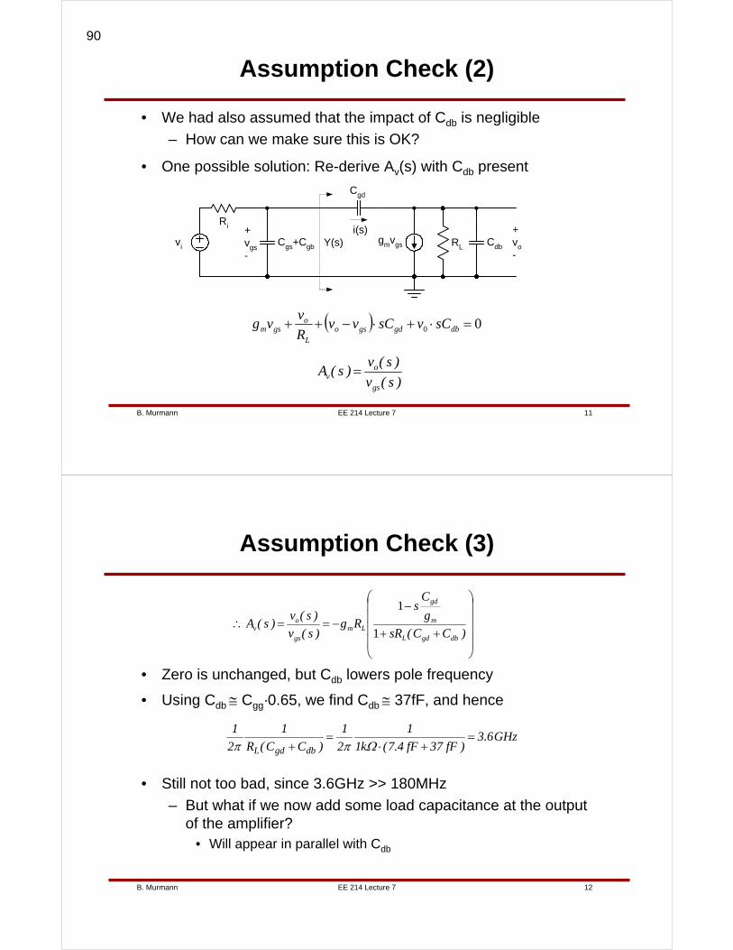
– How can we make sure this is OK?
• One possible solution: Re-derive Av(s) with Cdb present
Cgs+Cgbgmvgs
+vgs-
+vo-
RL
Ri
vi
Cgd
Y(s)i(s)
Cdb
( ) 00 =⋅+⋅−++ dbgdgsoL
ogsm sCvsCvv
R
vvg
)s(v
)s(v)s(A
gs
ov =
EE 214 Lecture 7B. Murmann 12
Assumption Check (3)
• Zero is unchanged, but Cdb lowers pole frequency
• Using Cdb ≅ Cgg·0.65, we find Cdb ≅ 37fF, and hence
⎟⎟⎟⎟
⎠
⎞
⎜⎜⎜⎜
⎝
⎛
++
−−==∴
)CC(sR
g
Cs
Rg)s(v
)s(v)s(A
dbgdL
m
gd
Lmgs
ov 1
1
GHz6.3)fF37fF4.7(k1
1
2
1
)CC(R
1
2
1
dbgdL=
+⋅=
+ Ωππ
• Still not too bad, since 3.6GHz >> 180MHz
– But what if we now add some load capacitance at the output of the amplifier?
• Will appear in parallel with Cdb
90
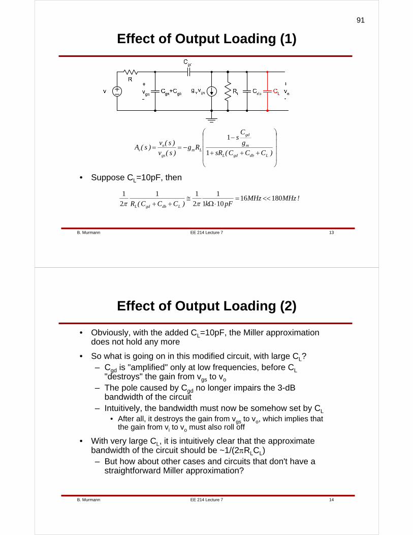
EE 214 Lecture 7B. Murmann 13
Effect of Output Loading (1)
⎟⎟⎟⎟
⎠
⎞
⎜⎜⎜⎜
⎝
⎛
+++
−−==
)CCC(sR
g
Cs
Rg)s(v
)s(v)s(A
LdbgdL
m
gd
Lmgs
ov 1
1
• Suppose CL=10pF, then
! MHzMHzpFk)CCC(R LdbgdL
18016101
1
2
11
2
1<<=
⋅Ω≅
++ ππ
EE 214 Lecture 7B. Murmann 14
Effect of Output Loading (2)
• Obviously, with the added CL=10pF, the Miller approximation does not hold any more
• So what is going on in this modified circuit, with large CL?– Cgd is "amplified" only at low frequencies, before CL
"destroys" the gain from vgs to vo
– The pole caused by Cgd no longer impairs the 3-dB bandwidth of the circuit
– Intuitively, the bandwidth must now be somehow set by CL
• After all, it destroys the gain from vgs to vo, which implies that the gain from vi to vo must also roll off
• With very large CL, it is intuitively clear that the approximate bandwidth of the circuit should be ~1/(2πRLCL)– But how about other cases and circuits that don't have a
straightforward Miller approximation?
91
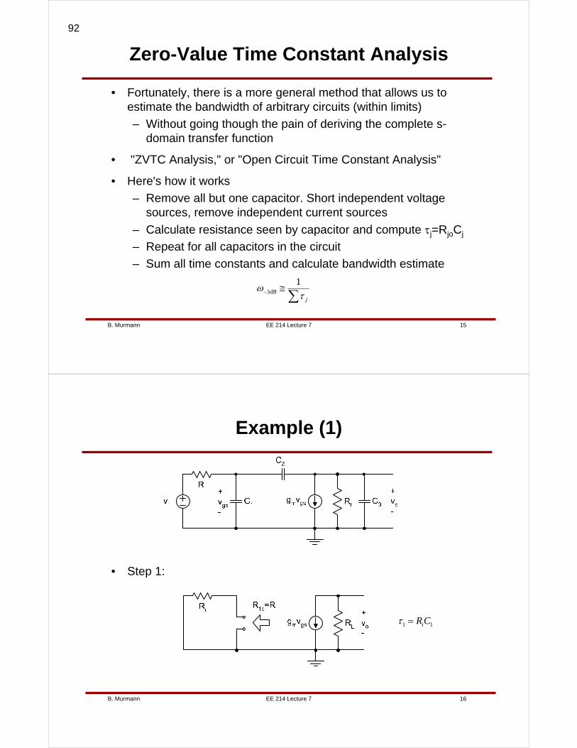
EE 214 Lecture 7B. Murmann 15
Zero-Value Time Constant Analysis
• Fortunately, there is a more general method that allows us to estimate the bandwidth of arbitrary circuits (within limits)
– Without going though the pain of deriving the complete s-domain transfer function
• "ZVTC Analysis," or "Open Circuit Time Constant Analysis"
• Here's how it works
– Remove all but one capacitor. Short independent voltage sources, remove independent current sources
– Calculate resistance seen by capacitor and compute τj=RjoCj
– Repeat for all capacitors in the circuit
– Sum all time constants and calculate bandwidth estimate
∑≅−
jdB τ
ω 13
EE 214 Lecture 7B. Murmann 16
Example (1)
• Step 1:
11 CRi=τ
92
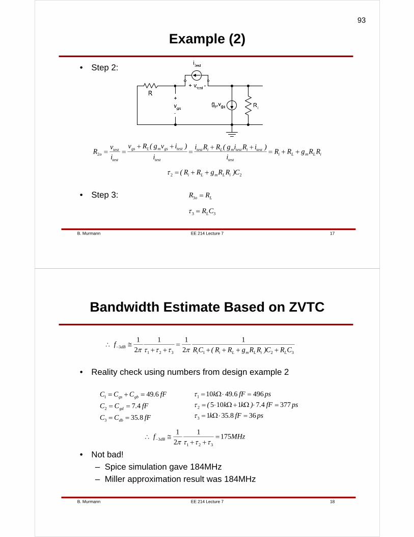
EE 214 Lecture 7B. Murmann 17
Example (2)
iLmLitest
testitestmLitest
test
testgsmLgs
test
testo RRgRR
i
)iRig(RRi
i
)ivg(Rv
i
vR ++=
++=
++==2
• Step 2:
• Step 3:
33 CRL=τ
22 C)RRgRR( iLmLi ++=τ
Lo RR =3
EE 214 Lecture 7B. Murmann 18
Bandwidth Estimate Based on ZVTC
• Reality check using numbers from design example 2
3213213
1
2
11
2
1
CRC)RRgRR(CRf
LiLmLiidB ++++
=++
≅∴ − πτττπ
fF.CC
fF.CC
fF.CCC
db
gd
gbgs
835
47
649
3
2
1
==
==
=+=
psfF.k
psfF.)kk(
psfF.k
368351
377471105
49664910
3
2
1
=⋅Ω==⋅Ω+Ω⋅=
=⋅Ω=
τττ
MHzf dB 1751
2
1
3213 =
++≅∴ − τττπ
• Not bad!
– Spice simulation gave 184MHz
– Miller approximation result was 184MHz
93
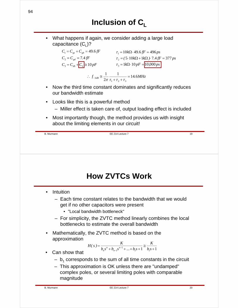
EE 214 Lecture 7B. Murmann 19
Inclusion of CL
• What happens if again, we consider adding a large load capacitance (CL)?
pFCCC
fF.CC
fF.CCC
Ldb
gd
gbgs
10
47
649
3
2
1
≅+=
==
=+=
ps,pFk
psfF.)kk(
psfF.k
00010101
377471105
49664910
3
2
1
=⋅Ω==⋅Ω+Ω⋅=
=⋅Ω=
τττ
MHz.f dB 6141
2
1
3213 =
++≅∴ − τττπ
• Now the third time constant dominates and significantly reduces our bandwidth estimate
• Looks like this is a powerful method
– Miller effect is taken care of, output loading effect is included
• Most importantly though, the method provides us with insight about the limiting elements in our circuit!
EE 214 Lecture 7B. Murmann 20
How ZVTCs Work
• Intuition
– Each time constant relates to the bandwidth that we would get if no other capacitors were present
• "Local bandwidth bottleneck"
– For simplicity, the ZVTC method linearly combines the local bottlenecks to estimate the overall bandwidth
• Mathematically, the ZVTC method is based on the approximation
11 111
1 +≅
++++= −
− sb
K
sb...sbsb
K)s(H
nn
nn
• Can show that
– b1 corresponds to the sum of all time constants in the circuit
– This approximation is OK unless there are "undamped" complex poles, or several limiting poles with comparable magnitude
94
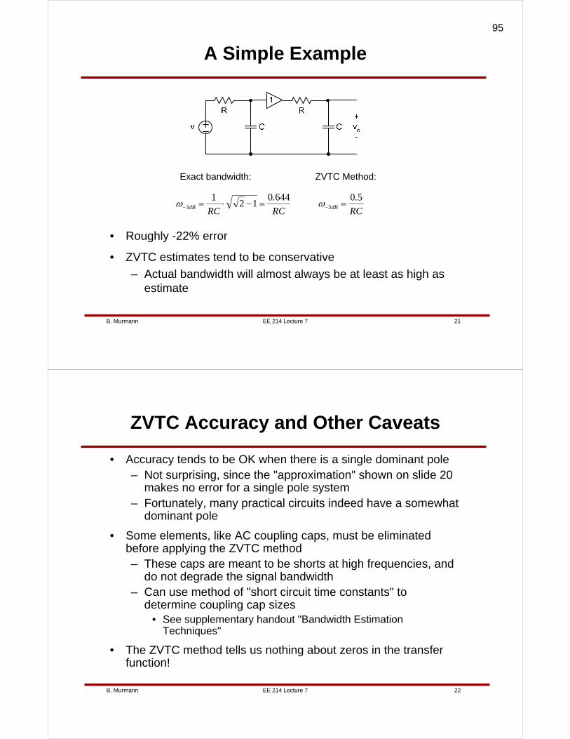
EE 214 Lecture 7B. Murmann 21
A Simple Example
• Roughly -22% error
• ZVTC estimates tend to be conservative
– Actual bandwidth will almost always be at least as high as estimate
RC
.
RC
.
RC dBdB
50644012
133 ==−⋅= −− ωω
Exact bandwidth: ZVTC Method:
EE 214 Lecture 7B. Murmann 22
ZVTC Accuracy and Other Caveats
• Accuracy tends to be OK when there is a single dominant pole– Not surprising, since the "approximation" shown on slide 20
makes no error for a single pole system– Fortunately, many practical circuits indeed have a somewhat
dominant pole
• Some elements, like AC coupling caps, must be eliminated before applying the ZVTC method– These caps are meant to be shorts at high frequencies, and
do not degrade the signal bandwidth– Can use method of "short circuit time constants" to
determine coupling cap sizes• See supplementary handout "Bandwidth Estimation
Techniques"
• The ZVTC method tells us nothing about zeros in the transfer function!
95

EE 214 Lecture 8B. Murmann 1
Lecture 8Electronic Noise
Boris MurmannStanford University
Copyright © 2007 by Boris Murmann
EE 214 Lecture 8B. Murmann 2
Overview
• Reading
– 11.1 (Noise Introduction)
– 11.2.2 (Thermal Noise)
– 11.3.3 (MOS Transistor Noise)
– Supplementary Handout: "Introduction to Noise" by Daniel Cooley
• Introduction
– Electronic noise is a significant and fundamental issue in the design of high performance analog circuits. The noise level of a circuit affects the "fidelity" or accuracy of the signals that are beingprocessed. As we shall see, minimizing electronic noise is costly; there exists a steep tradeoff with power dissipation and bandwidth. Today's lecture will provide an introduction to electronic noise at the component level (resistors and MOSFETs). We will use these results in the remainder of the course to analyze the impact of noise in various circuits.
96
EE 214 Lecture 8B. Murmann 3
Types of Noise
• "Man made noise", interference noise
– Signal coupling
– Substrate coupling
– Finite power supply rejection
– Solutions• Fully differential circuits
• Layout techniques
• "Electronic noise" or "device noise" (focus of this lecture)
– Fundamental• E.g. "thermal noise" caused by random motion of carriers
– Technology related• "Flicker noise" caused by material defects and "roughness"
EE 214 Lecture 8B. Murmann 4
Significance of Electronic Noise (1)
"Signal" "Noise"
noise
2signal
noise
signal
P
V
P
PSNR ∝=
Signal-to-Noise Ratio
97
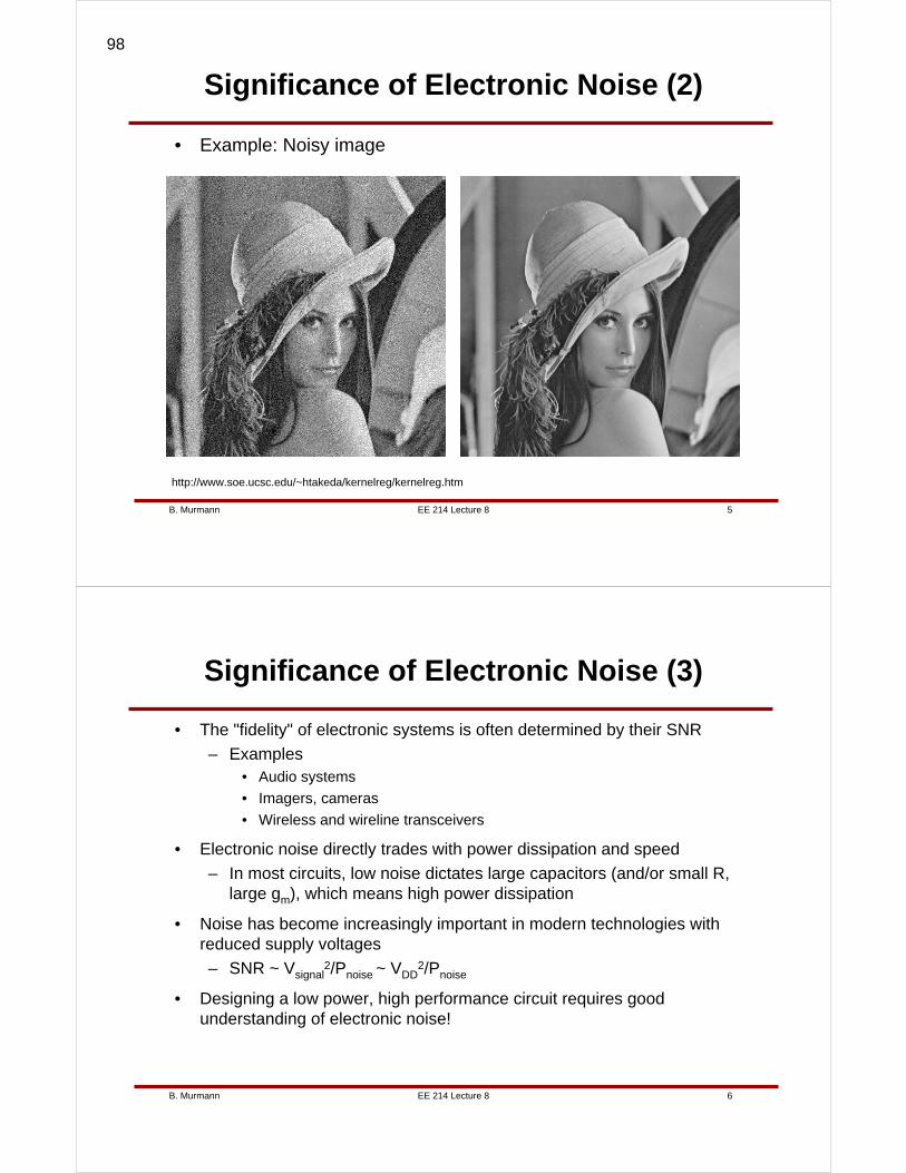
EE 214 Lecture 8B. Murmann 5
Significance of Electronic Noise (2)
• Example: Noisy image
http://www.soe.ucsc.edu/~htakeda/kernelreg/kernelreg.htm
EE 214 Lecture 8B. Murmann 6
Significance of Electronic Noise (3)
• The "fidelity" of electronic systems is often determined by their SNR
– Examples• Audio systems
• Imagers, cameras
• Wireless and wireline transceivers
• Electronic noise directly trades with power dissipation and speed
– In most circuits, low noise dictates large capacitors (and/or small R, large gm), which means high power dissipation
• Noise has become increasingly important in modern technologies with reduced supply voltages
– SNR ~ Vsignal2/Pnoise ~ VDD
2/Pnoise
• Designing a low power, high performance circuit requires good understanding of electronic noise!
98
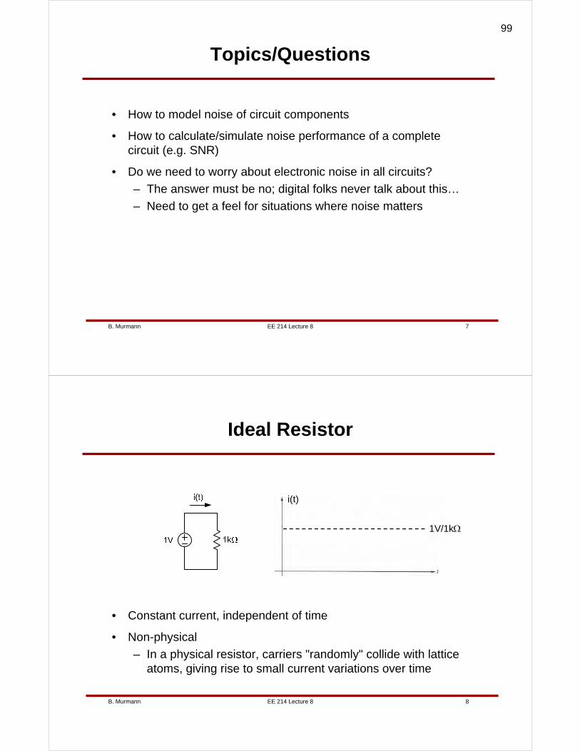
EE 214 Lecture 8B. Murmann 7
Topics/Questions
• How to model noise of circuit components
• How to calculate/simulate noise performance of a complete circuit (e.g. SNR)
• Do we need to worry about electronic noise in all circuits?
– The answer must be no; digital folks never talk about this…
– Need to get a feel for situations where noise matters
EE 214 Lecture 8B. Murmann 8
Ideal Resistor
• Constant current, independent of time
• Non-physical
– In a physical resistor, carriers "randomly" collide with latticeatoms, giving rise to small current variations over time
i(t)
1V/1kΩ
99

EE 214 Lecture 8B. Murmann 9
Physical Resistor
• "Thermal Noise" or "Johnson Noise"– J.B. Johnson, "Thermal Agitation of Electricity in Conductors,"
Phys. Rev., pp. 97-109, July 1928.
• Can model random current component e.g. using a noise current source in(t)
i(t)
1V/1kΩ
EE 214 Lecture 8B. Murmann 10
Properties of Thermal Noise
• Present in any conductor
• Independent of DC current flow
• Instantaneous noise value is unpredictable since it is a result of a large number of random, superimposed collisions with relaxation time constants of τ ≅ 0.17ps
– Consequences:• Gaussian amplitude distribution
• Knowing in(t) does not help predict in(t+Δt), unless Δt is on the order of 0.17ps (cannot sample signals this fast)
• The power generated by thermal noise is spread up to very high frequencies (1/τ ≅ 6,000Grad/s)
• The only predictable property of thermal noise is its average power!
100

EE 214 Lecture 8B. Murmann 11
Average Power
• For a deterministic current signal with period T, the average power is given by
( )∫−
⋅⋅=2/T
2/T
2av dtRti
T
1P
• This definition can be extended to capture non-deterministic random signals
– Assuming a real, stationary and ergodic random process
( )∫−
∞→⋅⋅=
2/T
2/T
2n
Tn dtRti
T
1limP
• For notational convenience, we typically drop R in the above expression and work with "mean square" current (or voltages)
( )∫−
∞→⋅=
2/T
2/T
2n
T
2n dtti
T
1limi
EE 214 Lecture 8B. Murmann 12
Thermal Noise Spectrum
• The so-called power spectral density (PSD) shows how much power a signal caries at a particular frequency
• In the case of thermal noise, the power is spread uniformly up to very high frequencies (about 10% drop at 2,000GHz)
PSD(f)
f
n0
• The total average noise power Pn in a particular frequency band can be found by integrating the PSD
( )∫ ⋅=2
1
f
f
n dffPSDP
101
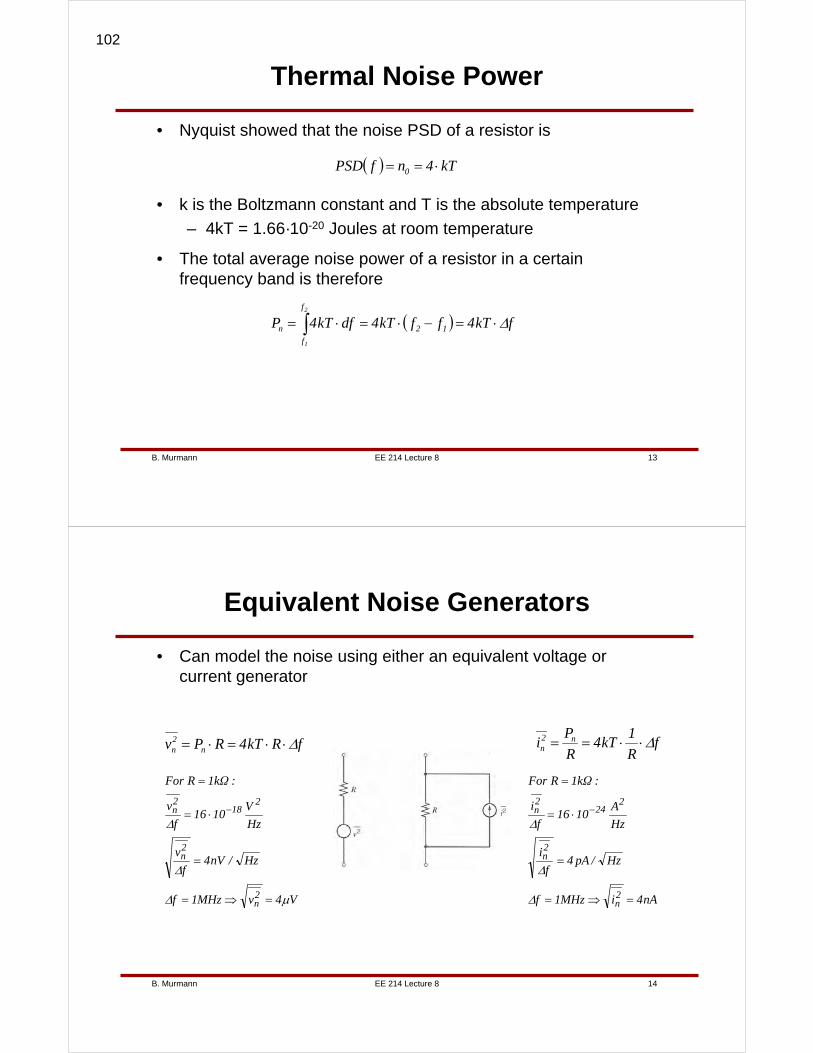
EE 214 Lecture 8B. Murmann 13
Thermal Noise Power
• Nyquist showed that the noise PSD of a resistor is
( ) kT4nfPSD 0 ⋅==
• k is the Boltzmann constant and T is the absolute temperature
– 4kT = 1.66·10-20 Joules at room temperature
• The total average noise power of a resistor in a certain frequency band is therefore
( ) fkT4ffkT4dfkT4P 12
f
f
n
2
1
Δ⋅=−⋅=⋅= ∫
EE 214 Lecture 8B. Murmann 14
Equivalent Noise Generators
• Can model the noise using either an equivalent voltage or current generator
fR
1kT4
R
Pi n2n Δ⋅⋅==fRkT4RPv n
2n Δ⋅⋅=⋅=
V4vMHz1f
Hz/nV4f
v
Hz
V1016
f
v
:1kΩR For
2n
2n
218
2n
μΔ
Δ
Δ
=⇒=
=
⋅=
=
−
nA4iMHz1f
Hz/pA4f
i
Hz
A1016
f
i
:1kΩR For
2n
2n
224
2n
=⇒=
=
⋅=
=
−
Δ
Δ
Δ
102
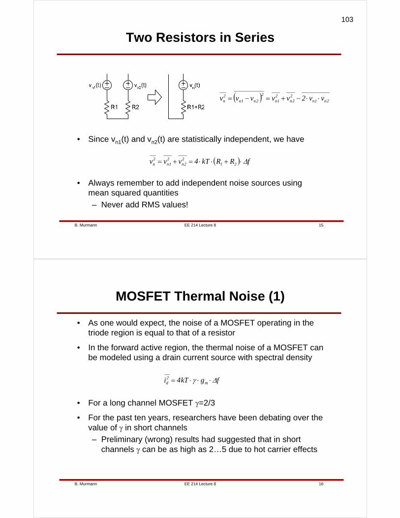
EE 214 Lecture 8B. Murmann 15
Two Resistors in Series
( ) fRRkT4vvv 2122n
21n
2n Δ⋅+⋅⋅=+=
• Always remember to add independent noise sources using mean squared quantities
– Never add RMS values!
( ) 2n1n22n
21n
2
2n1n2n vv2vvvvv ⋅⋅−+=−=
• Since vn1(t) and vn2(t) are statistically independent, we have
EE 214 Lecture 8B. Murmann 16
MOSFET Thermal Noise (1)
• As one would expect, the noise of a MOSFET operating in the triode region is equal to that of a resistor
• In the forward active region, the thermal noise of a MOSFET can be modeled using a drain current source with spectral density
fgkT4i m2d Δγ ⋅⋅⋅=
• For a long channel MOSFET γ=2/3
• For the past ten years, researchers have been debating over the value of γ in short channels
– Preliminary (wrong) results had suggested that in short channels γ can be as high as 2…5 due to hot carrier effects
103
EE 214 Lecture 8B. Murmann 17
MOSFET Thermal Noise (2)
• Fortunately, these discussions have come to an end with the conclusion that short channels have γ ≅ 1
– A. J. Scholten et al., "Noise modeling for RF CMOS circuit simulation," IEEE Trans. Electron Devices, pp. 618-632, Mar. 2003.
– R. P. Jindal, "Compact Noise Models for MOSFETs," IEEE Trans. Electron Devices, pp. 2051-2061, Sep. 2006.
[Scholten]
EE 214 Lecture 8B. Murmann 18
Spice Simulation (1)
* EE214 MOS device noise simulation
vd dd 0 1.5vm dd d 0 vg g 0 dc 0.8 ac 1mn1 d g 0 0 nch214 L=0.35u W=10uh1 c 0 ccvs vm 1
.op
.ac dec 100 10k 1gig
.noise v(c) vg
.options post brief
.lib './ee214_hspice.txt' nominal
.end
dd1.5V
d
0V c
CCVS1V/A
104
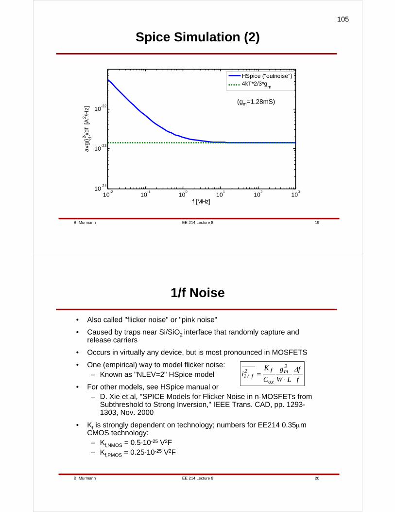
EE 214 Lecture 8B. Murmann 19
Spice Simulation (2)
10-2
10-1
100
101
102
103
10-24
10-23
10-22
f [MHz]
avg
(i d 2)/
df
[A2 /H
z]
HSpice ("outnoise")4kT*2/3*g
m
(gm=1.28mS)
EE 214 Lecture 8B. Murmann 20
1/f Noise
• Also called "flicker noise" or "pink noise"
• Caused by traps near Si/SiO2 interface that randomly capture and release carriers
• Occurs in virtually any device, but is most pronounced in MOSFETS
• One (empirical) way to model flicker noise:– Known as "NLEV=2" HSpice model
• For other models, see HSpice manual or– D. Xie et al, "SPICE Models for Flicker Noise in n-MOSFETs from
Subthreshold to Strong Inversion," IEEE Trans. CAD, pp. 1293-1303, Nov. 2000
• Kf is strongly dependent on technology; numbers for EE214 0.35μm CMOS technology:– Kf,NMOS = 0.5·10-25 V2F– Kf,PMOS = 0.25·10-25 V2F
f
f
LW
g
C
Ki
2m
ox
f2f/1
Δ⋅
=
105
EE 214 Lecture 8B. Murmann 21
1/f Noise Corner
• By definition, the frequency at which the flicker noise density equals the thermal noise density
fgkT4f
f
LW
g
C
Km
co
2m
ox
f ΔγΔ⋅⋅=
⋅
⎟⎠
⎞⎜⎝
⎛⎟⎟⎠
⎞⎜⎜⎝
⎛=
⋅=⇒
W
I
I
g
L
1
C
1
kT4
K
LW
g
C
1
kT4
Kf
D
D
m
ox
f
m
ox
fco
γ
γ
• Example: NMOS, L=0.35μm, gm/ID=10V-1 → ID/W=10A/m
⇒ fco = 244kHz
• In more recent technologies, 1/f corner frequencies can be on the order of 10MHz
EE 214 Lecture 8B. Murmann 22
1/f Noise Contribution (1)
• Just as with white noise, the total 1/f noise contribution is found by integrating its spectral density
⎟⎟⎠
⎞⎜⎜⎝
⎛⋅
=⎟⎟⎠
⎞⎜⎜⎝
⎛⋅
=
⋅= ∫
1
22m
ox
f
1
22m
ox
f
f
f
2m
ox
f2tot,f/1
f
flog3.2
LW
g
C
K
f
fln
LW
g
C
K
f
f
LW
g
C
Ki
2
1
Δ
• Total flicker noise depends on number of frequency decades
– Same flicker noise power in 1…10 Hz as in 1…10 GHz
– RMS noise proportional to sqrt(# of frequency decades)
• So, does flicker noise matter?
– Look at noise integral to see its relative contribution to totaldrain current noise
106
EE 214 Lecture 8B. Murmann 23
1/f Noise Contribution (2)
• For circuits with "high bandwidth", flicker noise is often insignificant
– Beware of exceptions…
102
104
106
108
10-23
10-22
10-21
10-20
f [Hz]
Sp
ect
rum
[A2 /H
z]
102
104
106
108
0
50
100
f [Hz]
Sq
rt(I
nte
gra
l) [n
A]
EE 214 Lecture 8B. Murmann 24
Lower Integration Limit
• Does the flicker noise PSD go to infinity for f→0? Fun discussions in– E. Milotti, "1/f noise: a pedagogical review," available at
http://arxiv.org/abs/physics/0204033
• Even if the PSD goes to infinity, do we care?– Let's say we are sensing a signal for a very long time (down
to a very low frequency), e.g.• 1 year ≅ 32 Msec, 1/year ≅ 0.03 μHz
– Number of frequency decades in 1/year to 100Hz ≅ 10• Means instead of 7 decades, we'd now have 17 in the previous
example• sqrt(17/7) = 1.56 → Only 56% more flicker noise!
• More fun reading on flicker noise– H. Schmid, "Aaargh! I just loooove flicker noise," IEEE Circuits and
Systems Magazine, Vol.7, Issue 1, pp. 32-35, 2007.
107
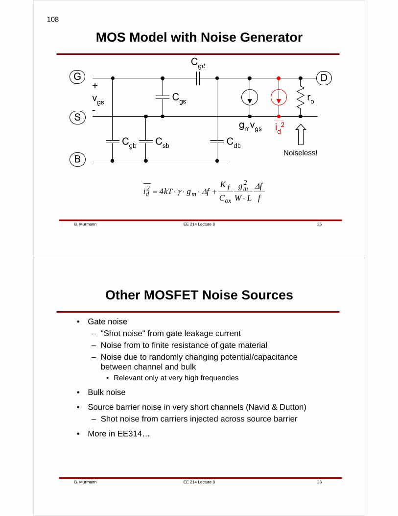
EE 214 Lecture 8B. Murmann 25
MOS Model with Noise Generator
Noiseless!
f
f
LW
g
C
KfgkT4i
2m
ox
fm
2d
ΔΔγ⋅
+⋅⋅⋅=
EE 214 Lecture 8B. Murmann 26
Other MOSFET Noise Sources
• Gate noise
– "Shot noise" from gate leakage current
– Noise from to finite resistance of gate material
– Noise due to randomly changing potential/capacitance between channel and bulk
• Relevant only at very high frequencies
• Bulk noise
• Source barrier noise in very short channels (Navid & Dutton)
– Shot noise from carriers injected across source barrier
• More in EE314…
108

EE 214 Lecture 9B. Murmann 1
Lecture 9Electronic Noise (Continued)
Boris MurmannStanford University
Copyright © 2007 by Boris Murmann
EE 214 Lecture 9B. Murmann 2
Overview
• Reading
– 11.4 (Circuit Noise Calculations)
– 11.5 (Equivalent Input Noise Generators)
– 11.9 (Noise Bandwidth)
• Introduction
– Having established the basic noise mechanisms in MOSFETS, today's lecture looks at noise in circuits. We will learn how to calculate the signal-to-noise ratio in a basic RC circuit and a common source amplifier. These examples are useful prerequisites for analyzing more complicated circuits (e.g. OTAs, later in this class). Furthermore, we will use these simple examples to develop a basic feel for the relevance of noise and associated tradeoffs.
109
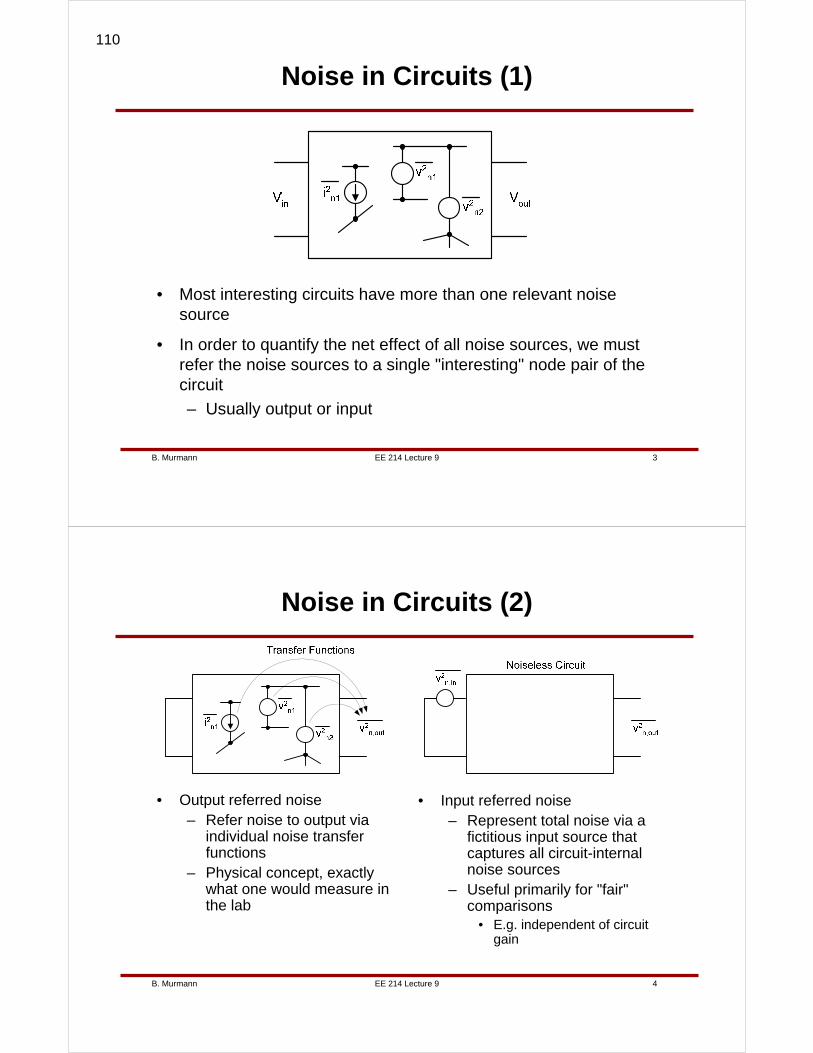
EE 214 Lecture 9B. Murmann 3
Noise in Circuits (1)
• Most interesting circuits have more than one relevant noise source
• In order to quantify the net effect of all noise sources, we must refer the noise sources to a single "interesting" node pair of the circuit
– Usually output or input
EE 214 Lecture 9B. Murmann 4
Noise in Circuits (2)
• Output referred noise– Refer noise to output via
individual noise transfer functions
– Physical concept, exactly what one would measure in the lab
• Input referred noise– Represent total noise via a
fictitious input source that captures all circuit-internal noise sources
– Useful primarily for "fair" comparisons
• E.g. independent of circuit gain
110
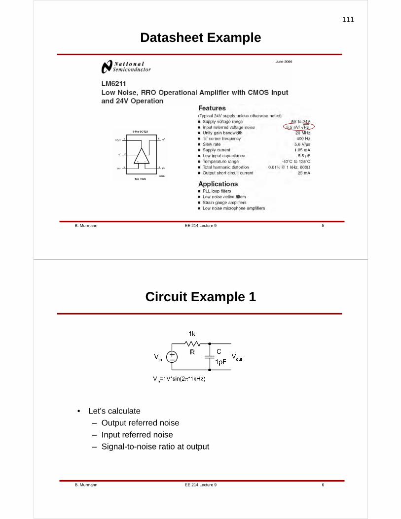
EE 214 Lecture 9B. Murmann 5
Datasheet Example
EE 214 Lecture 9B. Murmann 6
Circuit Example 1
• Let's calculate
– Output referred noise
– Input referred noise
– Signal-to-noise ratio at output
111
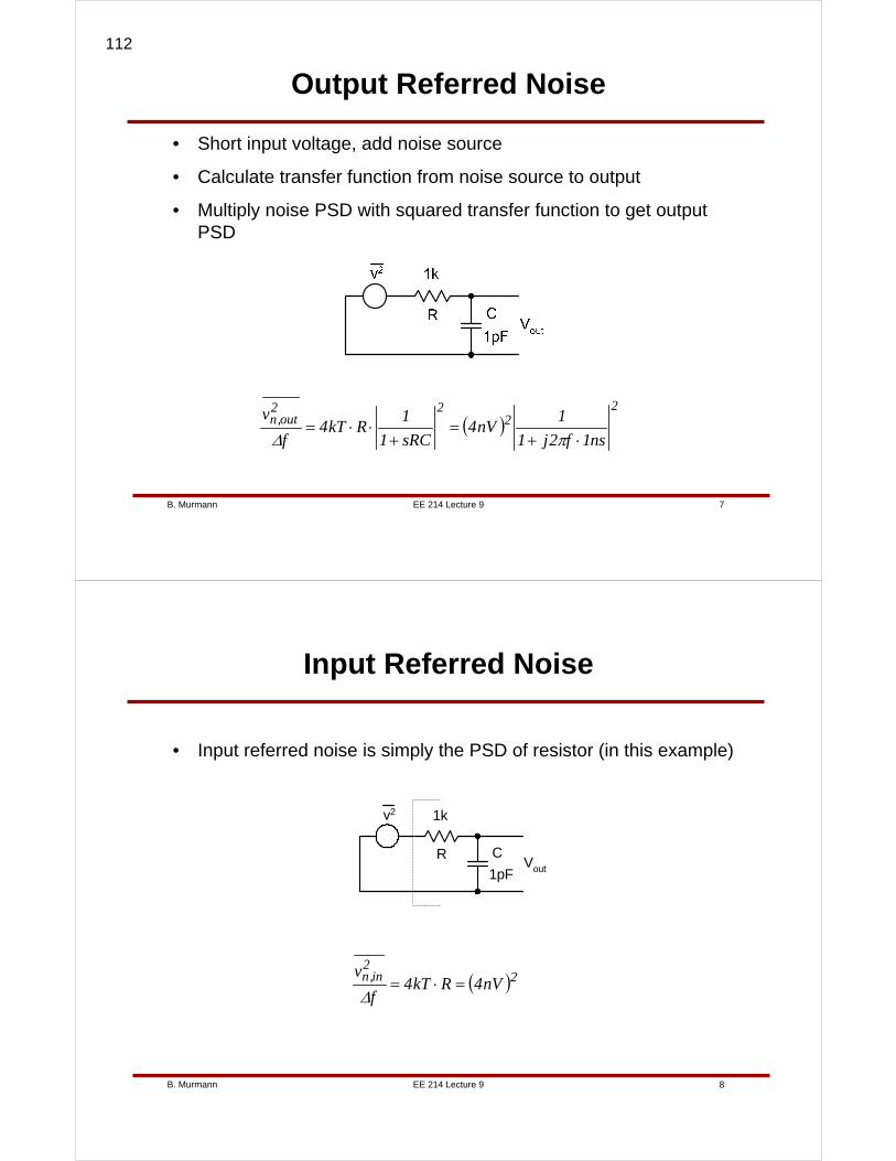
EE 214 Lecture 9B. Murmann 7
Output Referred Noise
( )2
222
out,n
ns1f2j1
1nV4
sRC1
1RkT4
f
v
⋅+=
+⋅⋅=
πΔ
• Short input voltage, add noise source
• Calculate transfer function from noise source to output
• Multiply noise PSD with squared transfer function to get output PSD
EE 214 Lecture 9B. Murmann 8
Input Referred Noise
RVout
1k
C
1pF
v2
( )22
in,n nV4RkT4f
v=⋅=
Δ
• Input referred noise is simply the PSD of resistor (in this example)
112
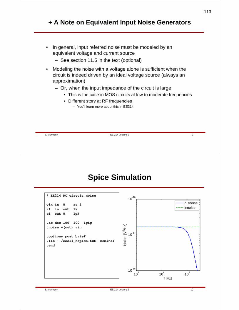
EE 214 Lecture 9B. Murmann 9
+ A Note on Equivalent Input Noise Generators
• In general, input referred noise must be modeled by an equivalent voltage and current source
– See section 11.5 in the text (optional)
• Modeling the noise with a voltage alone is sufficient when the circuit is indeed driven by an ideal voltage source (always an approximation)
– Or, when the input impedance of the circuit is large• This is the case in MOS circuits at low to moderate frequencies
• Different story at RF frequencies– You'll learn more about this in EE314
EE 214 Lecture 9B. Murmann 10
Spice Simulation
* EE214 RC circuit noise
vin in 0 ac 1r1 in out 1kc1 out 0 1pF
.ac dec 100 100 1gig
.noise v(out) vin
.options post brief
.lib './ee214_hspice.txt' nominal
.end
104
106
108
10-18
10-17
10-16
f [Hz]
No
ise
[V
2 /Hz]
outnoiseinnoise
113

EE 214 Lecture 9B. Murmann 11
Signal-to-Noise Ratio
• Over which bandwidth should we integrate the noise?
• Two interesting cases
– The output is measured or observed by a system with finite bandwidth (e.g. human ear)
• Use frequency range of that system as integration limits
• Applies on a case by case basis
– "Total integrated noise"
∫ ⋅
==2
1
f
f
2out,n
2peak,out
noise
signal
dff
v
V2
1
P
PSNR
Δ
EE 214 Lecture 9B. Murmann 12
Total Integrated Noise (1)
• Interesting result
– Total integrated noise at the output depends only on C (even though R is generating the noise)
C
kTdf
RCf2j1
1RkT4v
0
22
tot,out,n =⋅+
⋅⋅= ∫∞
π
• Simply the integral over all frequencies (zero to infinity)
• Relevant metric when output is observed without (significant) band limiting or when the output is sampled (e.g. switched capacitor circuits)
• The total integrated noise in our circuit is
114
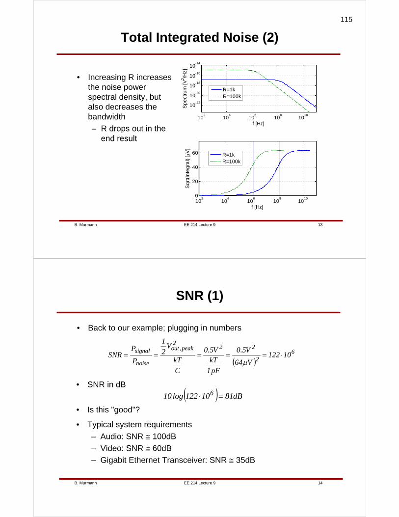
EE 214 Lecture 9B. Murmann 13
Total Integrated Noise (2)
• Increasing R increases the noise power spectral density, but also decreases the bandwidth
– R drops out in the end result
102
104
106
108
1010
10-22
10-20
10-18
10-16
10-14
f [Hz]
Sp
ect
rum
[V2 /H
z]
102
104
106
108
1010
0
20
40
60
f [Hz]
Sq
rt(I
nte
gra
l) [ μ
V]
R=1kR=100k
R=1kR=100k
EE 214 Lecture 9B. Murmann 14
SNR (1)
( ) dB8110122log10 6 =⋅
• Back to our example; plugging in numbers
( )6
2
222
peak,out
noise
signal10122
V64
V5.0
pF1
kTV5.0
C
kT
V2
1
P
PSNR ⋅=====
μ
• SNR in dB
• Is this "good"?
• Typical system requirements
– Audio: SNR ≅ 100dB
– Video: SNR ≅ 60dB
– Gigabit Ethernet Transceiver: SNR ≅ 35dB
115
EE 214 Lecture 9B. Murmann 15
SNR (2)
• Assuming Vout,peak = 1V
SNR [dB] C [pF]20 0.0000008340 0.00008360 0.008380 0.83
100 83120 8300140 830000
Hard to make such small capacitors…
Designer will definitely be concerned about thermal noise, capacitor sizes set by SNR
"Hardcore" thermal noise battle…
• General rules of thumb
– Up to SNR ~ 40dB, integrated circuits are usually not limited by thermal noise
– Achieving SNR >100dB is extremely difficult• Must usually rely on external components or "tricks" (such as
oversampling, see EE315)
EE 214 Lecture 9B. Murmann 16
MDS and DR
• Minimum detectable signal (MDS)
– A somewhat arbitrary definition
– Quantifies the signal level in a circuit that yields SNR=1; i.e.noise power = signal power
• Dynamic range (DR)
MDS
PDR
max,signal=
• If the noise level in the circuit is independent of the signal level (not always the case), it follows that the DR is equal to the "peak SNR", i.e. the SNR with the maximum signal applied
116
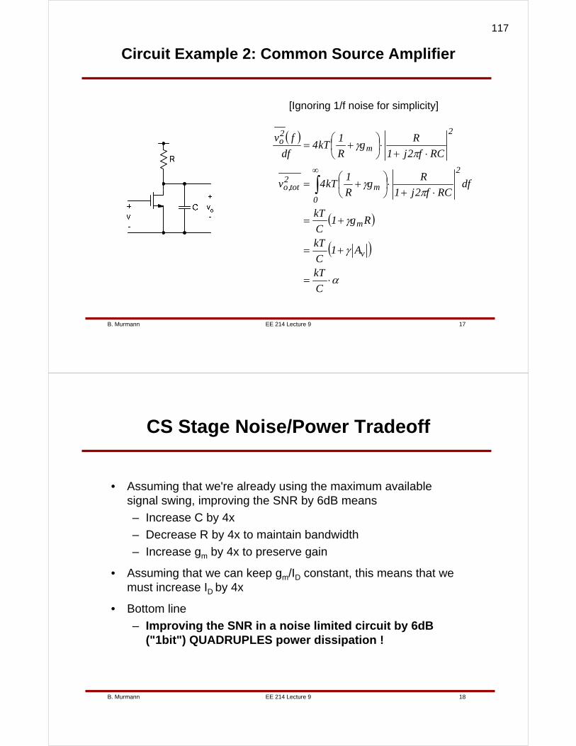
EE 214 Lecture 9B. Murmann 17
Circuit Example 2: Common Source Amplifier
( )
( )
( )
α
γ
γ
πγ
πγ
⋅=
+=
+=
⋅+⋅⎟⎠⎞
⎜⎝⎛ +=
⋅+⋅⎟⎠⎞
⎜⎝⎛ +=
∫∞
C
kT
A1C
kT
Rg1C
kT
dfRCf2j1
Rg
R
1kT4v
RCf2j1
Rg
R
1kT4
df
fv
v
m
0
2
m2
tot,o
2
m
2o
[Ignoring 1/f noise for simplicity]
EE 214 Lecture 9B. Murmann 18
CS Stage Noise/Power Tradeoff
• Assuming that we're already using the maximum available signal swing, improving the SNR by 6dB means
– Increase C by 4x
– Decrease R by 4x to maintain bandwidth
– Increase gm by 4x to preserve gain
• Assuming that we can keep gm/ID constant, this means that we must increase ID by 4x
• Bottom line
– Improving the SNR in a noise limited circuit by 6dB ("1bit") QUADRUPLES power dissipation !
117

EE 214 Lecture 10B. Murmann 1
Lecture 10Backgate Effect
Common Gate Stage
Boris MurmannStanford University
Copyright © 2007 by Boris Murmann
EE 214 Lecture 10B. Murmann 2
Overview
• Reading– 1.6.6 (Body Transconductance)– 3.3.4, 7.2.4.2 (Common Gate Stage)– 3.4.2.2, 7.3.4 (up to p. 526) (Cascode Stage)
• Introduction– Having completed our discussion of simple common source
amplifiers, we now continue by exploring alternative ways of building single transistor stages. First, we will look at the common gate (CG) stage, followed by a discussion of the common drain (CD) stage in the next lecture. While CS stages can usually be configured with source and bulk nodes tied together, this is often not the case in the CG and CD configurations. Hence, we'll first need to take a look at the socalled backgate effect (sometimes called "body effect") which becomes relevant in this context.
Somewhat tedious to read…
118
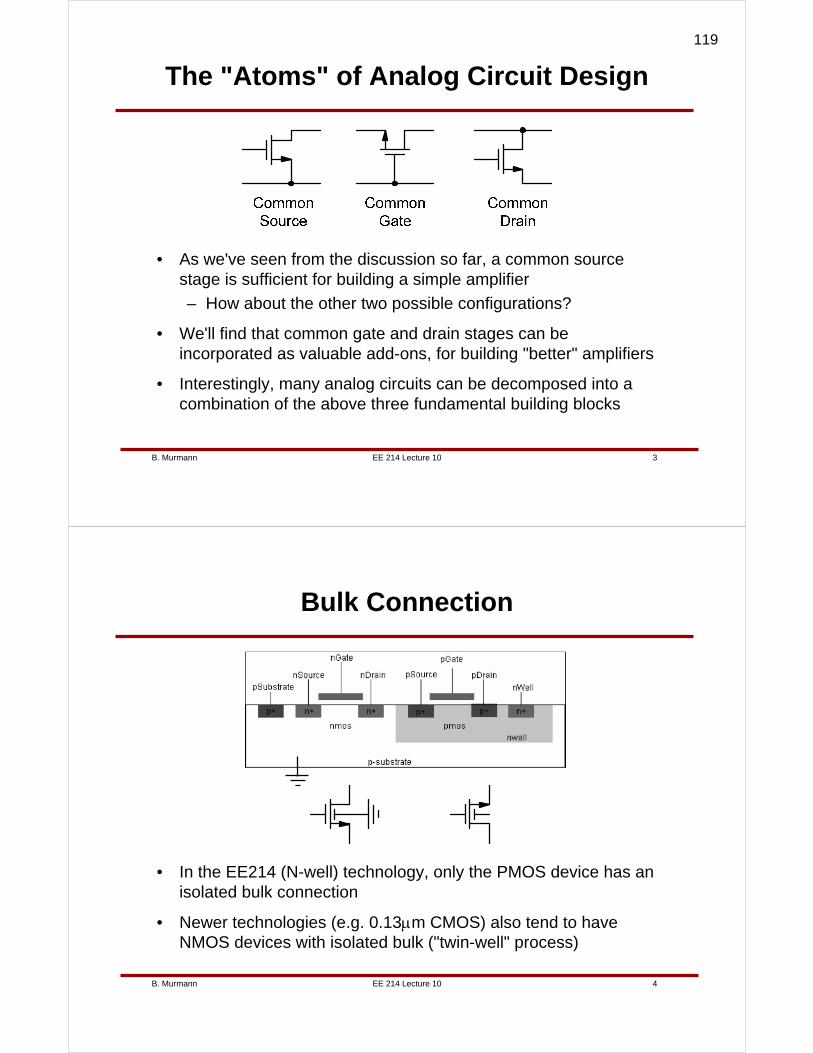
EE 214 Lecture 10B. Murmann 3
The "Atoms" of Analog Circuit Design
• As we've seen from the discussion so far, a common source stage is sufficient for building a simple amplifier
– How about the other two possible configurations?
• We'll find that common gate and drain stages can be incorporated as valuable add-ons, for building "better" amplifiers
• Interestingly, many analog circuits can be decomposed into a combination of the above three fundamental building blocks
EE 214 Lecture 10B. Murmann 4
Bulk Connection
• In the EE214 (N-well) technology, only the PMOS device has an isolated bulk connection
• Newer technologies (e.g. 0.13μm CMOS) also tend to have NMOS devices with isolated bulk ("twin-well" process)
119
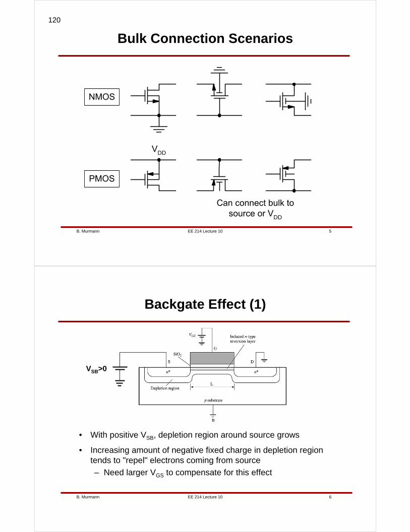
EE 214 Lecture 10B. Murmann 5
Bulk Connection Scenarios
DD
DD
EE 214 Lecture 10B. Murmann 6
Backgate Effect (1)
• With positive VSB, depletion region around source grows
• Increasing amount of negative fixed charge in depletion region tends to "repel" electrons coming from source
– Need larger VGS to compensate for this effect
VSB>0
120
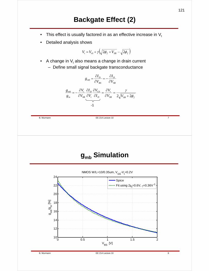
EE 214 Lecture 10B. Murmann 7
Backgate Effect (2)
• This effect is usually factored in as an effective increase in Vt
• Detailed analysis shows
( )fSBftt VVV φφγ 220 −++=
• A change in Vt also means a change in drain current
– Define small signal backgate transconductance
SB
D
BS
Dmb V
I
V
Ig
∂∂
−=∂∂
=
fSBSB
t
D
GS
t
D
SB
t
m
mb
VV
V
I
V
V
I
V
V
g
g
φγ
22 +=
∂∂
=∂∂
∂∂
∂∂
−=
-1
EE 214 Lecture 10B. Murmann 8
gmb Simulation
0 0.5 1 1.5 210
12
14
16
18
20
22
24
NMOS W/L=10/0.35um, VGS
-Vt=0.2V
VBS
[V]
gm
b/gm
[%]
Spice
Fit using 2φf=0.6V, γ=0.36V-1
121
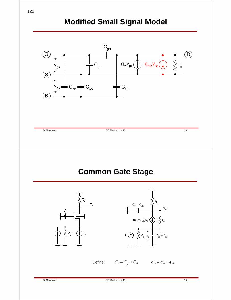
EE 214 Lecture 10B. Murmann 9
Modified Small Signal Model
EE 214 Lecture 10B. Murmann 10
Common Gate Stage
RS
RL
Vo
-(gm+gmb)vi
+vi-
ii Cgs+Csb
Cgd+Cdb
ro
mbmmsbgsS gg'gCCC +=+=Define:
122
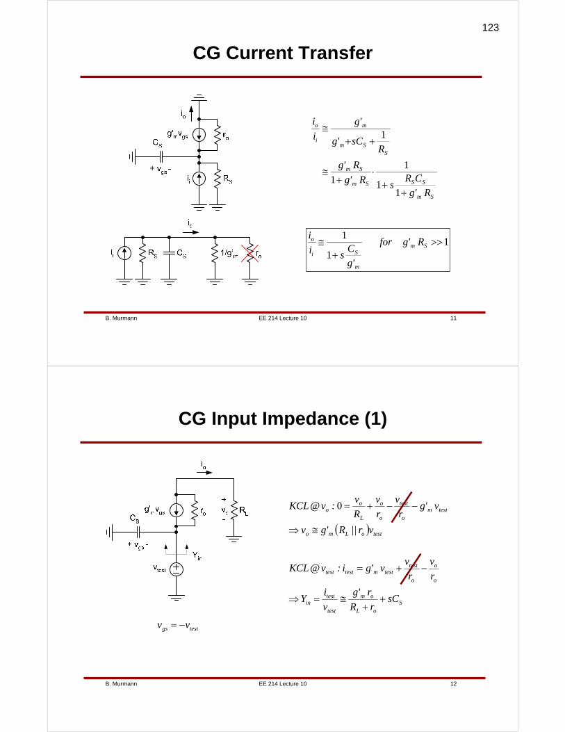
EE 214 Lecture 10B. Murmann 11
CG Current Transfer
11
1>>
+≅ Sm
m
Si
o R'gfor
'gC
si
i
Sm
SSSm
Sm
SSm
m
i
o
R'gCR
sR'g
R'g
RsC'g
'g
i
i
++
⋅+
≅
++≅
11
1
1
1
EE 214 Lecture 10B. Murmann 12
CG Input Impedance (1)
testgs vv −=
( )
SoL
om
test
testin
o
o
o
testtestmtesttest
testoLmo
testmo
test
o
o
L
oo
sCrR
r'g
v
iY
r
v
r
vv'gi:v@KCL
vr||R'gv
v'gr
v
r
v
R
v:v@KCL
++
≅=⇒
−+=
≅⇒
−−+=0
123
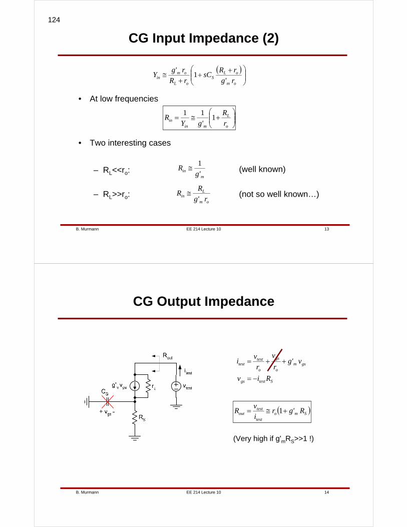
EE 214 Lecture 10B. Murmann 13
CG Input Impedance (2)
• At low frequencies
( )⎟⎟⎠
⎞⎜⎜⎝
⎛ ++
+≅
om
oLS
oL
omin r'g
rRsC
rR
r'gY 1
⎟⎟⎠
⎞⎜⎜⎝
⎛+≅=
o
L
minin r
R
'gYR 1
11
• Two interesting cases
– RL<<ro:
– RL>>ro:
min 'g
R1
≅
om
Lin r'g
RR ≅
(well known)
(not so well known…)
EE 214 Lecture 10B. Murmann 14
CG Output Impedance
Stestgs
gsmo
gs
o
testtest
Riv
v'gr
v
r
vi
−=
++=
( )Smotest
testout R'gr
i
vR +≅= 1
(Very high if g'mRS>>1 !)
124
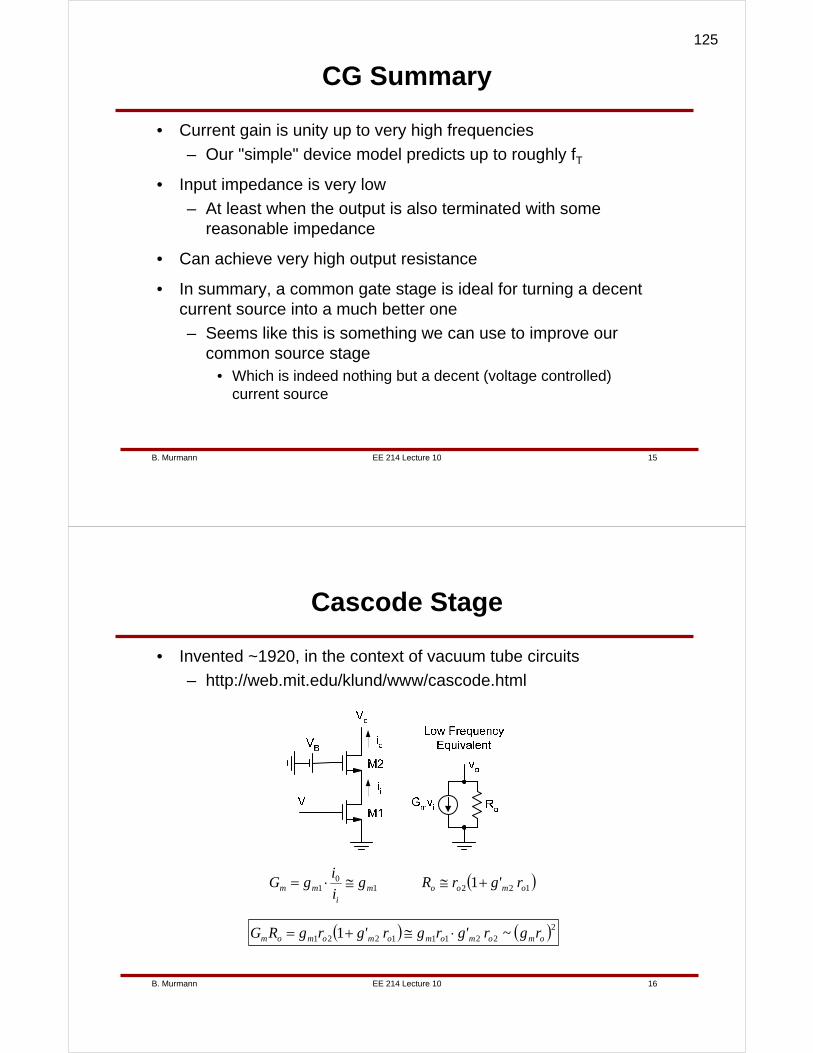
EE 214 Lecture 10B. Murmann 15
CG Summary
• Current gain is unity up to very high frequencies
– Our "simple" device model predicts up to roughly fT
• Input impedance is very low
– At least when the output is also terminated with some reasonable impedance
• Can achieve very high output resistance
• In summary, a common gate stage is ideal for turning a decent current source into a much better one
– Seems like this is something we can use to improve our common source stage
• Which is indeed nothing but a decent (voltage controlled) current source
EE 214 Lecture 10B. Murmann 16
Cascode Stage
• Invented ~1920, in the context of vacuum tube circuits
– http://web.mit.edu/klund/www/cascode.html
( )12210
1 1 omoomi
mm r'grRgi
igG +≅≅⋅=
( ) ( )222111221 1 omomomomomom rg~r'grgr'grgRG ⋅≅+=
125
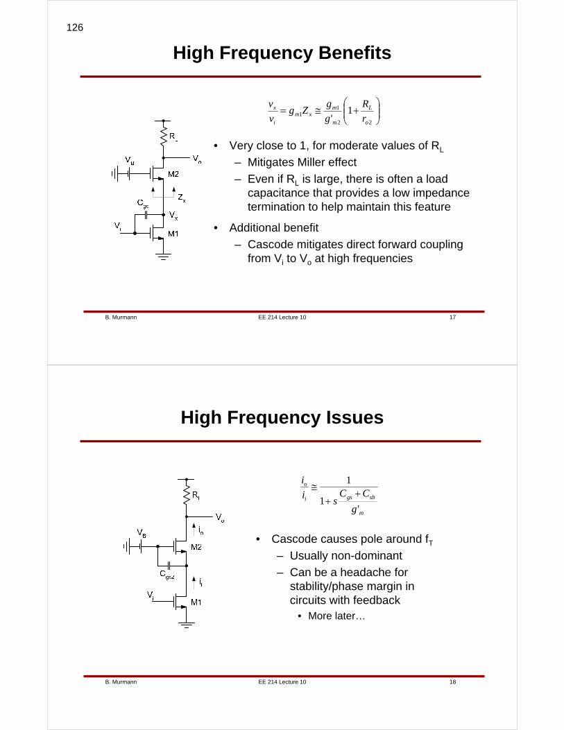
EE 214 Lecture 10B. Murmann 17
High Frequency Benefits
• Very close to 1, for moderate values of RL
– Mitigates Miller effect
– Even if RL is large, there is often a load capacitance that provides a low impedance termination to help maintain this feature
• Additional benefit
– Cascode mitigates direct forward coupling from Vi to Vo at high frequencies
⎟⎟⎠
⎞⎜⎜⎝
⎛+≅=
22
11 1
o
L
m
mxm
i
x
r
R
'g
gZg
v
v
EE 214 Lecture 10B. Murmann 18
High Frequency Issues
• Cascode causes pole around fT– Usually non-dominant
– Can be a headache for stability/phase margin in circuits with feedback
• More later…
m
sbgsi
o
'g
CCs
i
i+
+≅
1
1
126
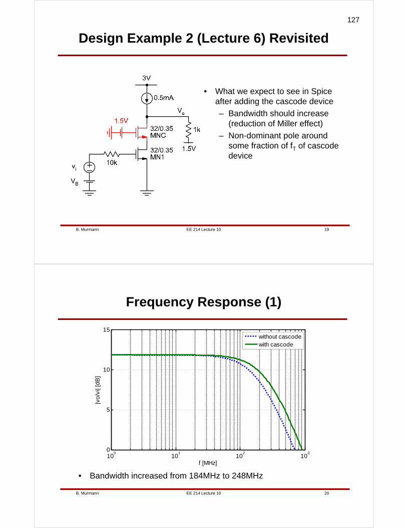
EE 214 Lecture 10B. Murmann 19
Design Example 2 (Lecture 6) Revisited
• What we expect to see in Spice after adding the cascode device
– Bandwidth should increase (reduction of Miller effect)
– Non-dominant pole around some fraction of fT of cascode device
EE 214 Lecture 10B. Murmann 20
Frequency Response (1)
• Bandwidth increased from 184MHz to 248MHz
100
101
102
103
0
5
10
15
f [MHz]
|vo
/vi|
[dB
]
without cascodewith cascode
127
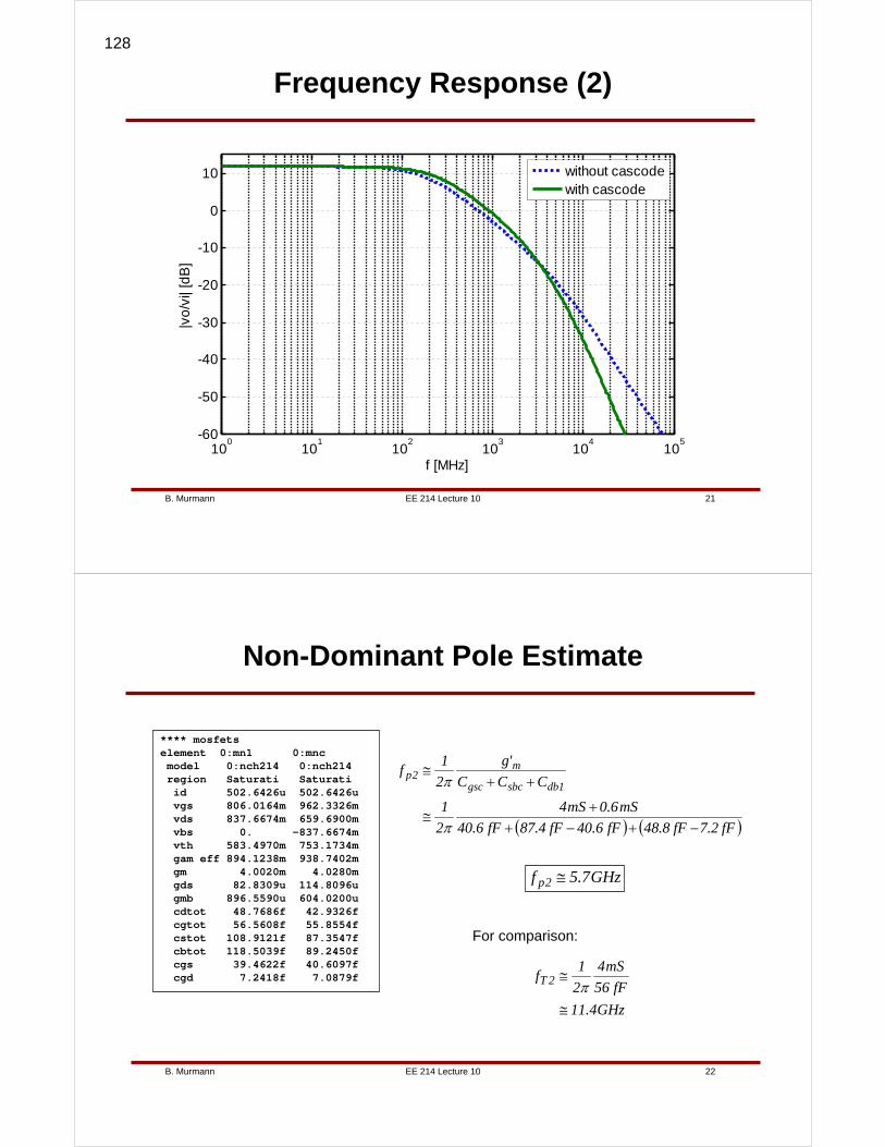
EE 214 Lecture 10B. Murmann 21
Frequency Response (2)
100
101
102
103
104
105
-60
-50
-40
-30
-20
-10
0
10
f [MHz]
|vo
/vi|
[dB
]
without cascodewith cascode
EE 214 Lecture 10B. Murmann 22
Non-Dominant Pole Estimate
**** mosfetselement 0:mn1 0:mnc model 0:nch214 0:nch214 region Saturati Saturatiid 502.6426u 502.6426uvgs 806.0164m 962.3326mvds 837.6674m 659.6900mvbs 0. -837.6674mvth 583.4970m 753.1734mgam eff 894.1238m 938.7402mgm 4.0020m 4.0280mgds 82.8309u 114.8096ugmb 896.5590u 604.0200ucdtot 48.7686f 42.9326fcgtot 56.5608f 55.8554fcstot 108.9121f 87.3547fcbtot 118.5039f 89.2450fcgs 39.4622f 40.6097fcgd 7.2418f 7.0879f
( ) ( )fF2.7fF8.48fF6.40fF4.87fF6.40
mS6.0mS4
2
1
CCC
'g
2
1f
1dbsbcgsc
m2p
−+−++
≅
++≅
π
π
GHz7.5f 2p ≅
GHz4.11
fF56
mS4
2
1f 2T
≅
≅π
For comparison:
128
EE 214 Lecture 10B. Murmann 23
Supply Headroom Issue
• Even if we adjust VB such that VDS1 is small, adding a cascode reduces the available signal swing
• This can be a big issue when designing circuits with VDD≅1V
– Typically need each VDS>~0.2V
– A severe dynamic range penalty
EE 214 Lecture 10B. Murmann 24
Cascode Noise
• It is typically argued that cascodes do not add a significant amount of noise
• A closer look reveals that cascodes can contribute significant noise at high frequencies
– Noise current A no longer compensates B at high frequencies
• We'll take a more quantitative look at this later in this course
VB
Vi
Vo
RL
VDD
i2n1
i2n2
VB
Vi
Vo
RL
VDD
i2n1
A
B
129

EE 214 Lecture 11B. Murmann 1
Lecture 11Common Drain Stage
(Source Follower)
Boris MurmannStanford University
Copyright © 2007 by Boris Murmann
EE 214 Lecture 11B. Murmann 2
Overview
• Reading
– 3.3.7 (Common Drain Stage)
– 7.2.2 (Frequency Response of Voltage Buffers)
– 5.3 (Source Follower as an Output Stage, optional)
• Introduction
– Last lecture, we have seen that a common gate stage has a fairly low input impedance, and high output impedance. The common drain stage that we'll analyze today exhibits the exact opposite features: High input impedance and low output impedance. After an analysis of relevant port characteristics, we will discuss some potential applications and also drawbacks of this circuit.
130
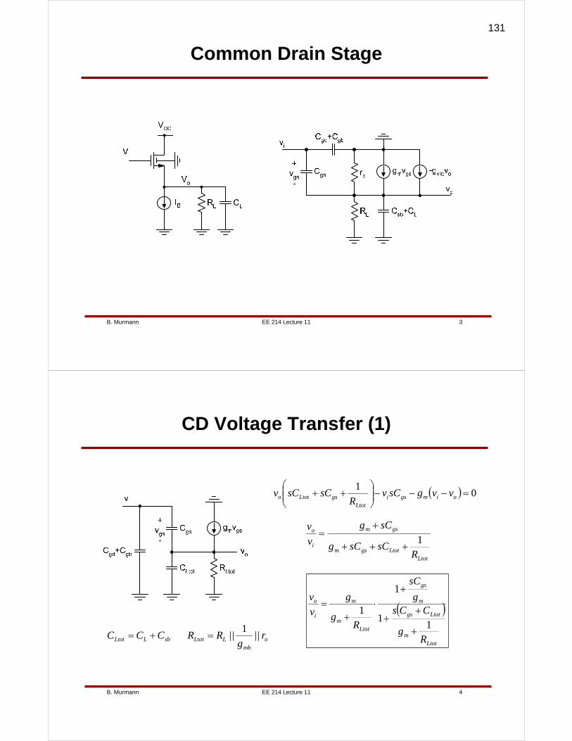
EE 214 Lecture 11B. Murmann 3
Common Drain Stage
EE 214 Lecture 11B. Murmann 4
CD Voltage Transfer (1)
LtotLtotgsm
gsm
i
o
RsCsCg
sCg
v
v1
+++
+=
( ) 01
=−−−⎟⎟⎠
⎞⎜⎜⎝
⎛++ oimgsi
LtotgsLtoto vvgsCv
RsCsCv
( )
Ltotm
Ltotgs
m
gs
Ltotm
m
i
o
Rg
CCsg
sC
Rg
g
v
v
11
1
1
+
++
+⋅
+=
omb
LLtotsbLLtot r||g
||RRCCC1
=+=
131
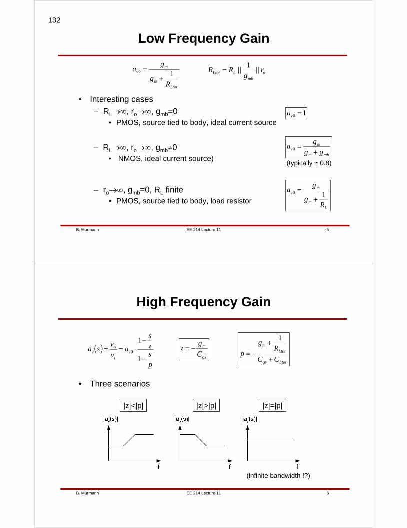
EE 214 Lecture 11B. Murmann 5
Low Frequency Gain
• Interesting cases
– RL→∞, ro→∞, gmb=0• PMOS, source tied to body, ideal current source
Ltotm
mv
Rg
ga
10
+=
omb
LLtot r||g
||RR1
=
10 =va
mbm
mv gg
ga
+=0– RL→∞, ro→∞, gmb≠0
• NMOS, ideal current source)(typically ≅ 0.8)
– ro→∞, gmb=0, RL finite• PMOS, source tied to body, load resistor
Lm
mv
Rg
ga
10
+=
EE 214 Lecture 11B. Murmann 6
High Frequency Gain
• Three scenarios
( )
pszs
av
vsa v
i
ov
−
−⋅==1
1
0gs
m
C
gz −=
Ltotgs
Ltotm
CC
Rg
p+
+−=
1
(infinite bandwidth !?)
|z|<|p| |z|>|p| |z|=|p|
132
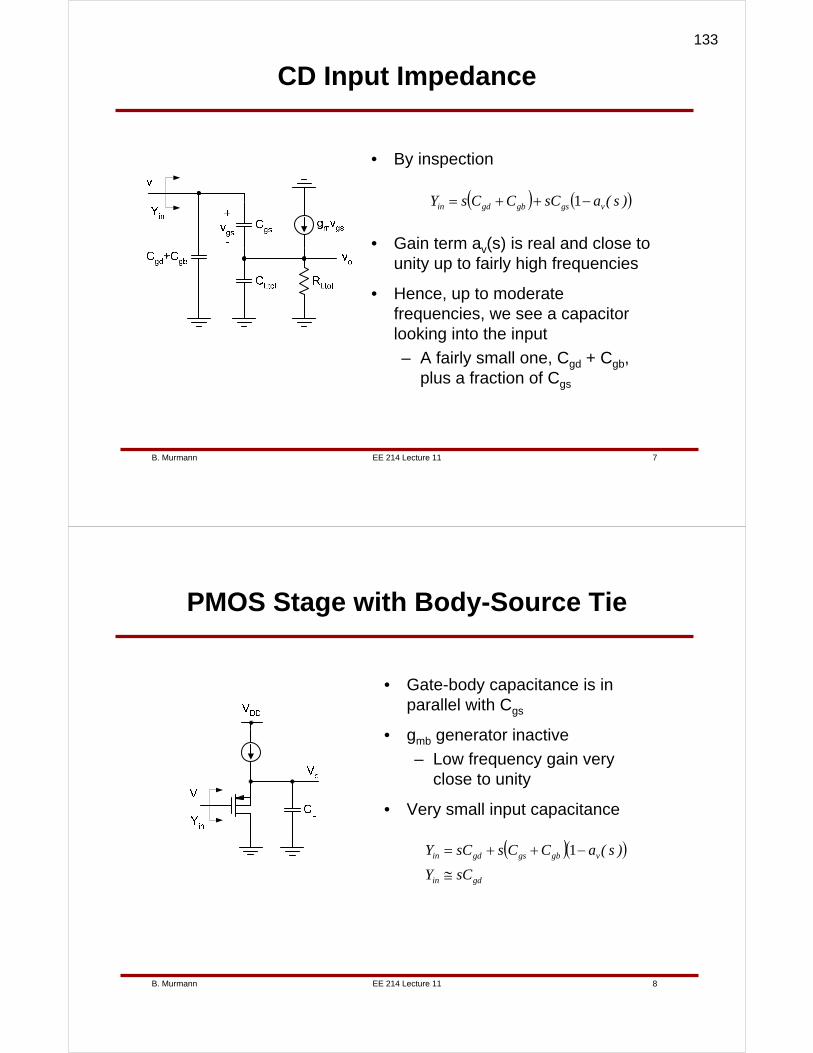
EE 214 Lecture 11B. Murmann 7
CD Input Impedance
• By inspection
( ) ( ))s(asCCCsY vgsgbgdin −++= 1
• Gain term av(s) is real and close to unity up to fairly high frequencies
• Hence, up to moderate frequencies, we see a capacitor looking into the input
– A fairly small one, Cgd + Cgb, plus a fraction of Cgs
EE 214 Lecture 11B. Murmann 8
PMOS Stage with Body-Source Tie
• Gate-body capacitance is in parallel with Cgs
• gmb generator inactive
– Low frequency gain very close to unity
• Very small input capacitance
( )( )gdin
vgbgsgdin
sCY
)s(aCCssCY
≅
−++= 1
133
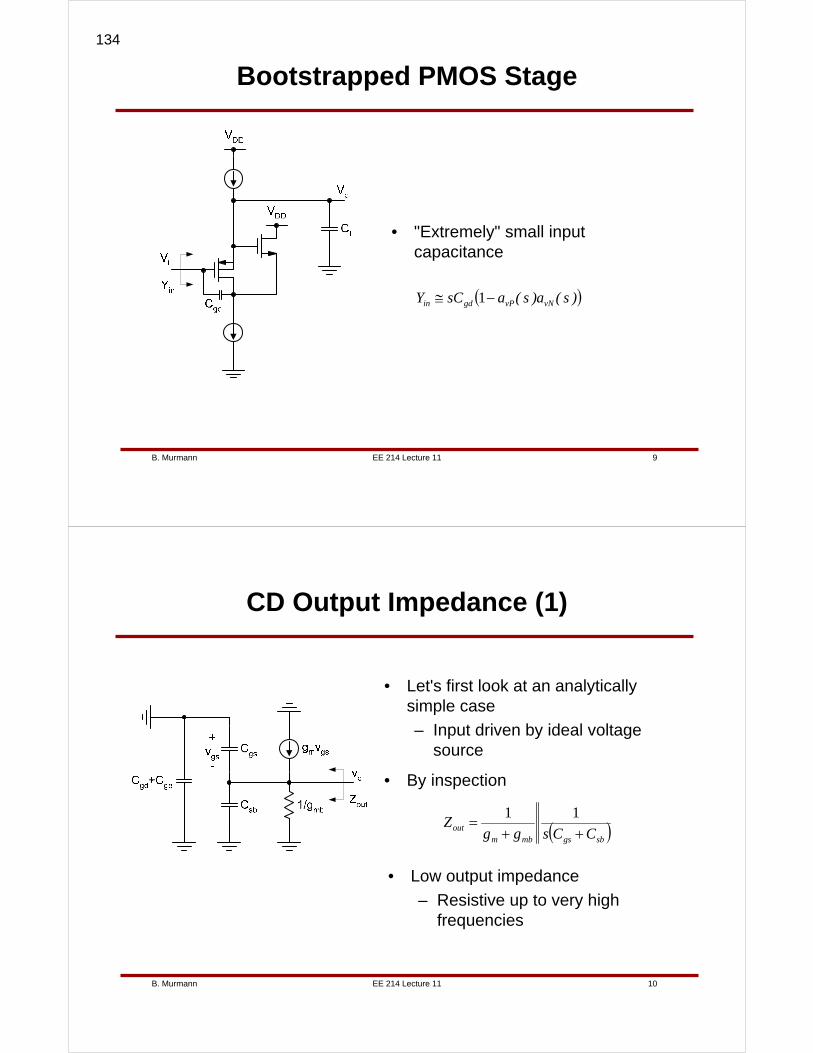
EE 214 Lecture 11B. Murmann 9
Bootstrapped PMOS Stage
• "Extremely" small input capacitance
( ))s(a)s(asCY vNvPgdin −≅ 1
EE 214 Lecture 11B. Murmann 10
CD Output Impedance (1)
• Let's first look at an analytically simple case
– Input driven by ideal voltage source
• By inspection
( )sbgsmbmout CCsgg
Z++
=11
• Low output impedance
– Resistive up to very high frequencies
134
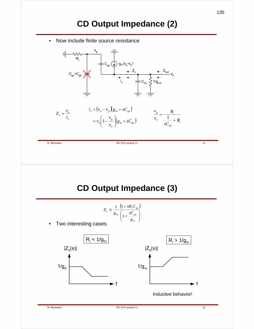
EE 214 Lecture 11B. Murmann 11
CD Output Impedance (2)
• Now include finite source resistance
( )( )
( )gsmo
go
gsmgox
sCgv
vv
sCgvvi
+⎟⎟⎠
⎞⎜⎜⎝
⎛−=
+−=
1x
ox i
vZ =
igs
i
o
g
RsC
R
v
v
+=
1
EE 214 Lecture 11B. Murmann 12
CD Output Impedance (3)
• Two interesting cases
( )
⎟⎟⎠
⎞⎜⎜⎝
⎛+
+≅
m
gs
gsi
mx
g
sC
CsR
gZ
1
11
Ri > 1/gmRi < 1/gm
Inductive behavior!
135
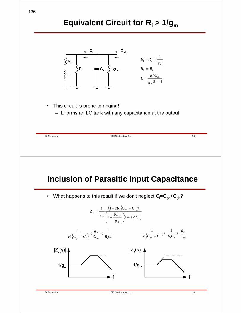
EE 214 Lecture 11B. Murmann 13
Equivalent Circuit for Ri > 1/gm
• This circuit is prone to ringing!
– L forms an LC tank with any capacitance at the output
1
1
2
2
21
−=
=
=
im
gsi
i
m
Rg
CRL
RR
gR||R
EE 214 Lecture 11B. Murmann 14
Inclusion of Parasitic Input Capacitance
( )( )ii
m
gs
igsi
mx
CsRg
sC
CCsR
gZ
+⎟⎟⎠
⎞⎜⎜⎝
⎛+
++=
11
11
• What happens to this result if we don’t neglect Ci=Cgd+Cgb?
gs
m
iiigsi C
g
CRCCR<<
+11
iigs
m
igsi CRC
g
CCR
11<<
+
136
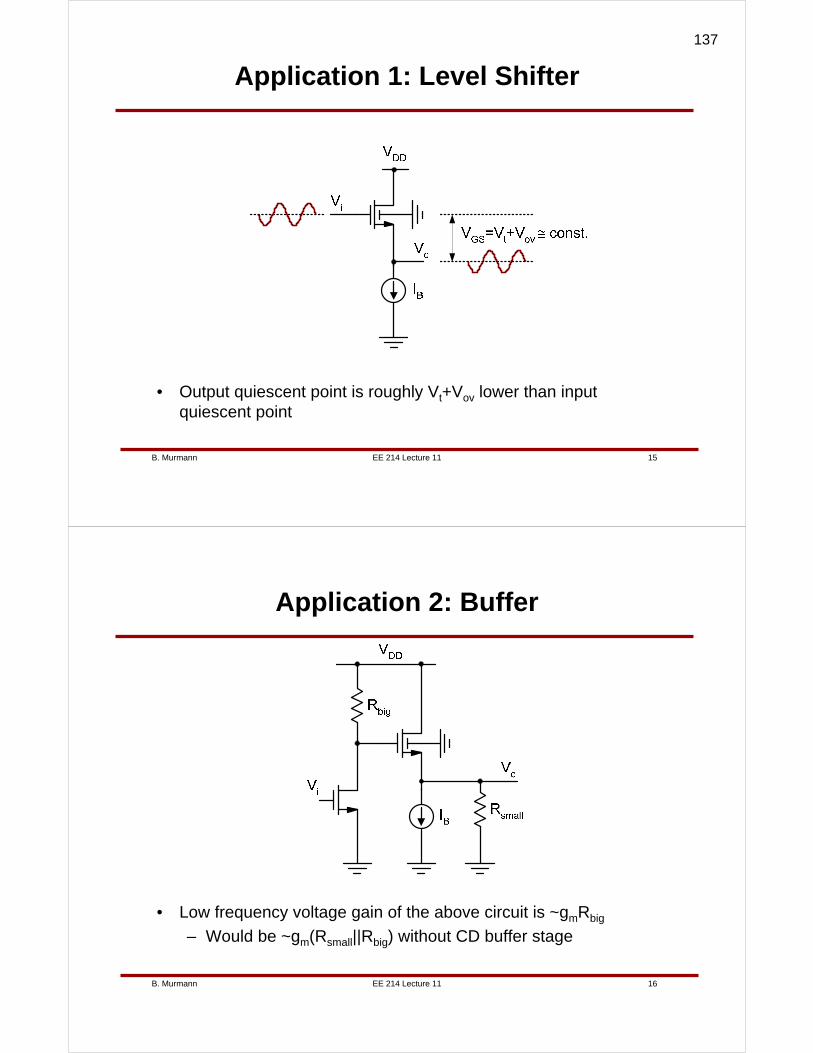
EE 214 Lecture 11B. Murmann 15
Application 1: Level Shifter
• Output quiescent point is roughly Vt+Vov lower than input quiescent point
EE 214 Lecture 11B. Murmann 16
Application 2: Buffer
• Low frequency voltage gain of the above circuit is ~gmRbig
– Would be ~gm(Rsmall||Rbig) without CD buffer stage
137
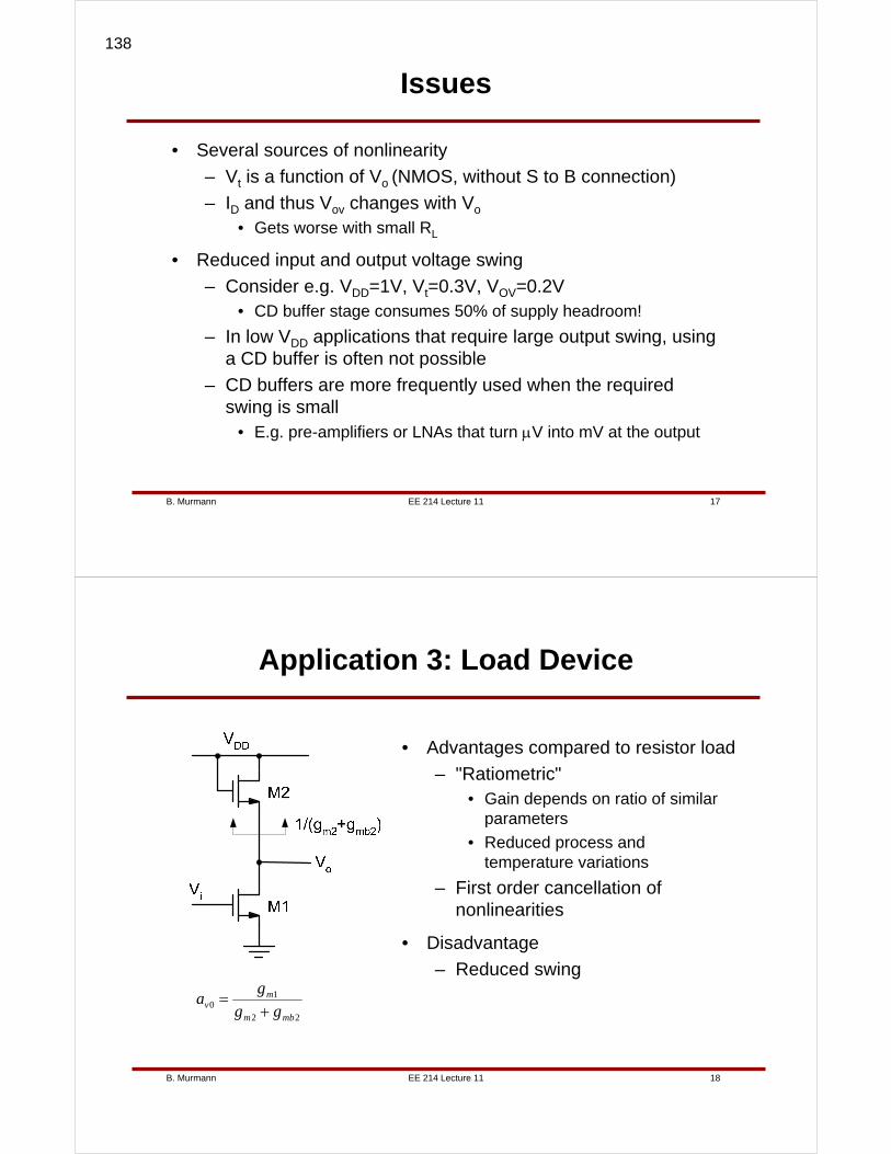
EE 214 Lecture 11B. Murmann 17
Issues
• Several sources of nonlinearity
– Vt is a function of Vo (NMOS, without S to B connection)
– ID and thus Vov changes with Vo
• Gets worse with small RL
• Reduced input and output voltage swing
– Consider e.g. VDD=1V, Vt=0.3V, VOV=0.2V• CD buffer stage consumes 50% of supply headroom!
– In low VDD applications that require large output swing, using a CD buffer is often not possible
– CD buffers are more frequently used when the required swing is small
• E.g. pre-amplifiers or LNAs that turn μV into mV at the output
EE 214 Lecture 11B. Murmann 18
Application 3: Load Device
• Advantages compared to resistor load
– "Ratiometric"• Gain depends on ratio of similar
parameters
• Reduced process and temperature variations
– First order cancellation of nonlinearities
• Disadvantage
– Reduced swing
22
10
mbm
mv gg
ga
+=
138

EE 214 Lecture 11B. Murmann 19
Summary – Elementary Transistor Stages
• Common source
– VCCS, makes a good voltage amplifier when terminated with a high impedance
• Common gate
– Typically low input impedance, high output impedance
– Can be used to improve the intrinsic voltage gain of a common source stage
• "Cascode" stage
• Common drain
– Typically high input impedance, low output impedance
– Great for shifting the DC operating point of signals
– Useful as a voltage buffer when swing and nonlinearity are not an issue
EE 214 Lecture 11B. Murmann 20
Practical Biasing Issues (1)
• Typically cannot afford to have sufficiently large decoupling cap for VB
• Also, may want to work with ground referenced input voltage
139
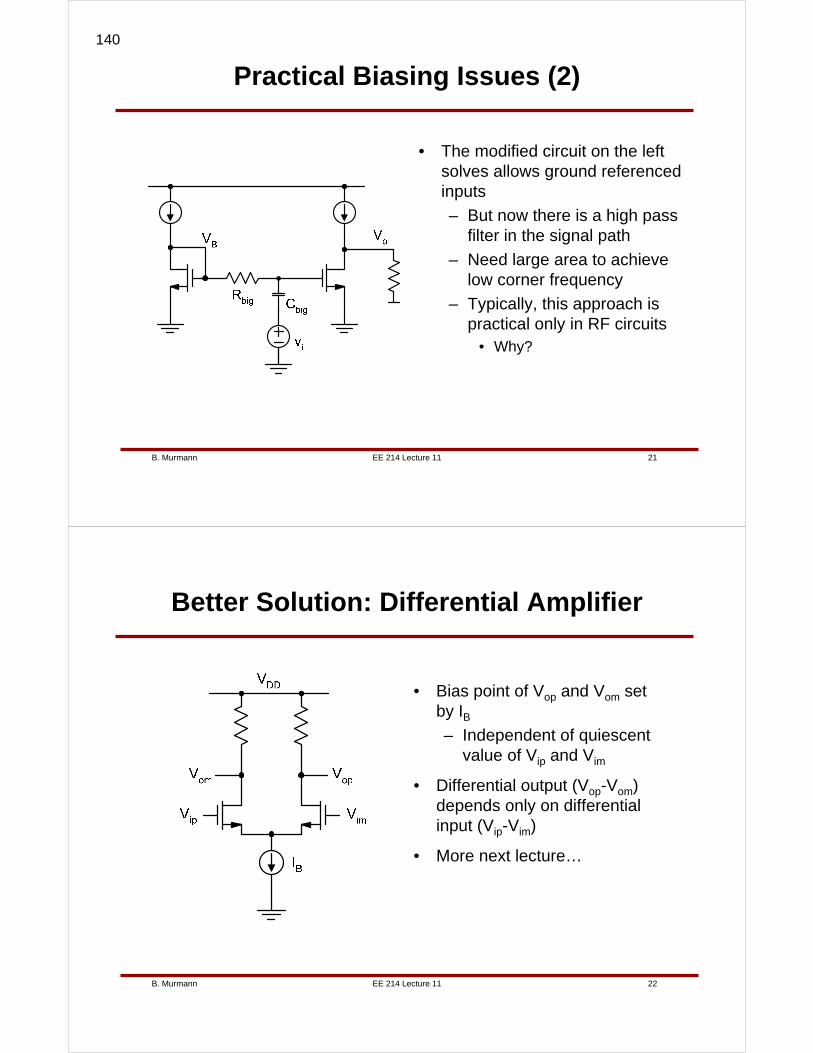
EE 214 Lecture 11B. Murmann 21
Practical Biasing Issues (2)
• The modified circuit on the left solves allows ground referenced inputs
– But now there is a high pass filter in the signal path
– Need large area to achieve low corner frequency
– Typically, this approach is practical only in RF circuits
• Why?
EE 214 Lecture 11B. Murmann 22
Better Solution: Differential Amplifier
• Bias point of Vop and Vom set by IB– Independent of quiescent
value of Vip and Vim
• Differential output (Vop-Vom) depends only on differential input (Vip-Vim)
• More next lecture…
140
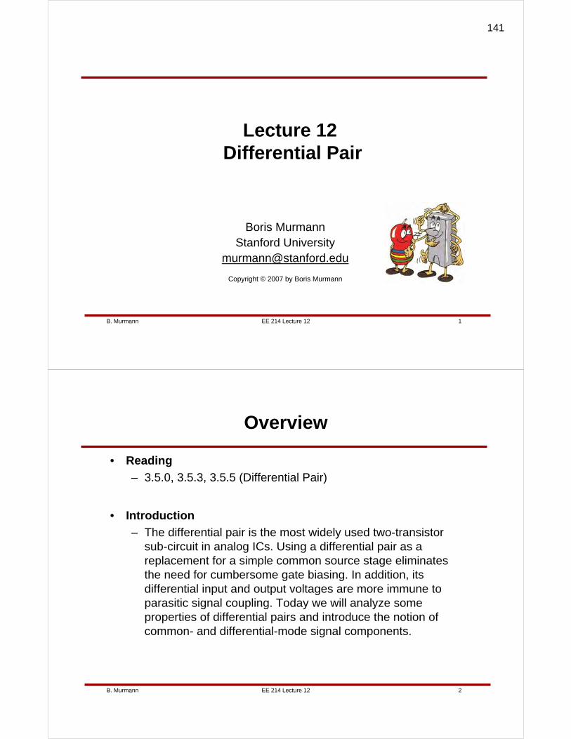
EE 214 Lecture 12B. Murmann 1
Lecture 12Differential Pair
Boris MurmannStanford University
Copyright © 2007 by Boris Murmann
EE 214 Lecture 12B. Murmann 2
Overview
• Reading
– 3.5.0, 3.5.3, 3.5.5 (Differential Pair)
• Introduction
– The differential pair is the most widely used two-transistor sub-circuit in analog ICs. Using a differential pair as a replacement for a simple common source stage eliminates the need for cumbersome gate biasing. In addition, its differential input and output voltages are more immune to parasitic signal coupling. Today we will analyze some properties of differential pairs and introduce the notion of common- and differential-mode signal components.
141
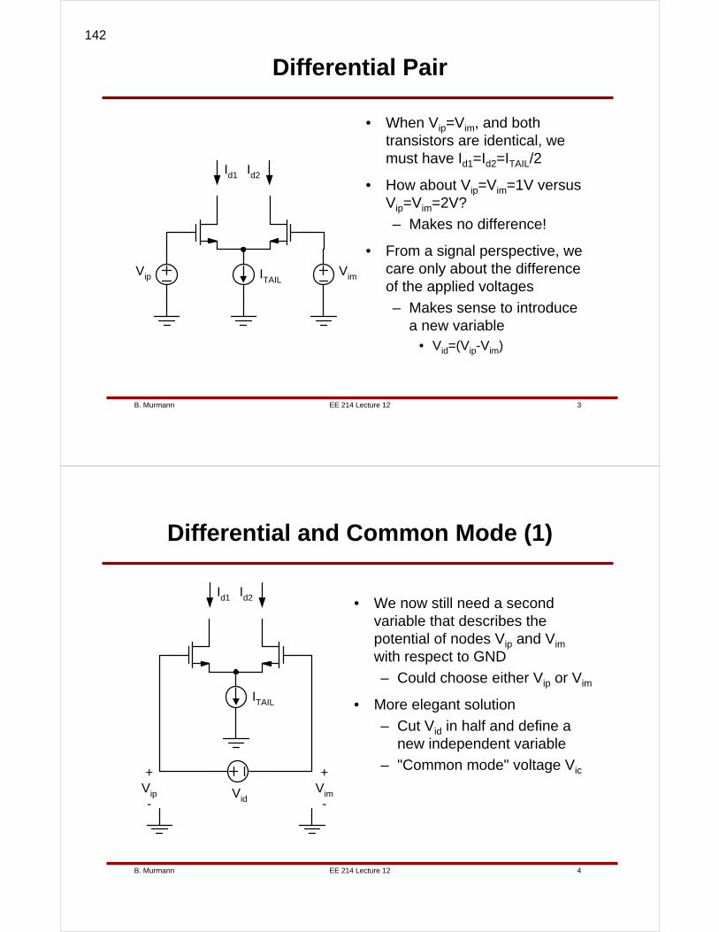
EE 214 Lecture 12B. Murmann 3
Differential Pair
• When Vip=Vim, and both transistors are identical, we must have Id1=Id2=ITAIL/2
• How about Vip=Vim=1V versus Vip=Vim=2V?
– Makes no difference!
• From a signal perspective, we care only about the difference of the applied voltages
– Makes sense to introduce a new variable
• Vid=(Vip-Vim)
ITAIL
Id1
Vip
Id2
Vim
EE 214 Lecture 12B. Murmann 4
Differential and Common Mode (1)
• We now still need a second variable that describes the potential of nodes Vip and Vim
with respect to GND
– Could choose either Vip or Vim
• More elegant solution
– Cut Vid in half and define a new independent variable
– "Common mode" voltage Vic
ITAIL
Id1
+Vip-
Id2
Vid
+Vim-
142
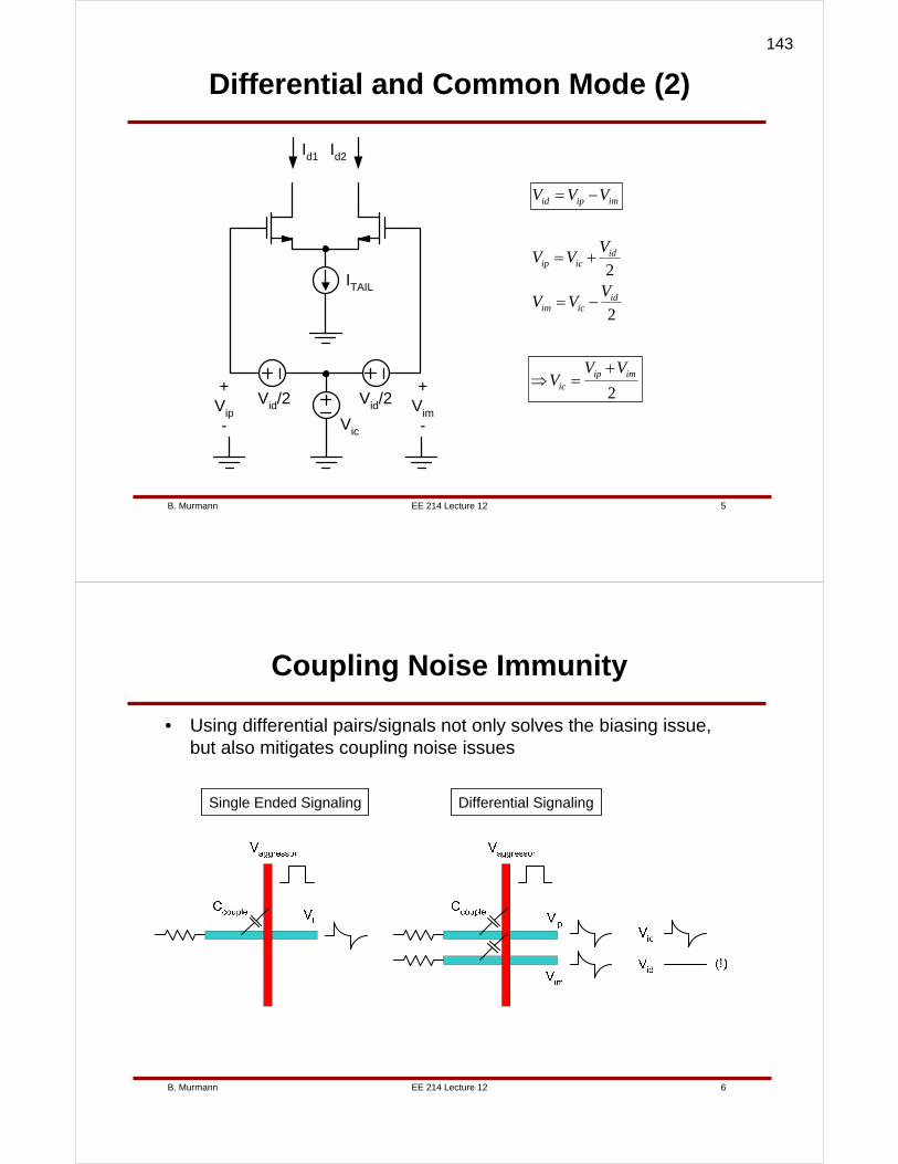
EE 214 Lecture 12B. Murmann 5
Differential and Common Mode (2)
ITAIL
Id1
+Vip-
Id2
Vid/2+
Vim-
Vid/2
Vic
imipid VVV −=
2
2
idicim
idicip
VVV
VVV
−=
+=
2imip
ic
VVV
+=⇒
EE 214 Lecture 12B. Murmann 6
Coupling Noise Immunity
• Using differential pairs/signals not only solves the biasing issue, but also mitigates coupling noise issues
Single Ended Signaling Differential Signaling
143
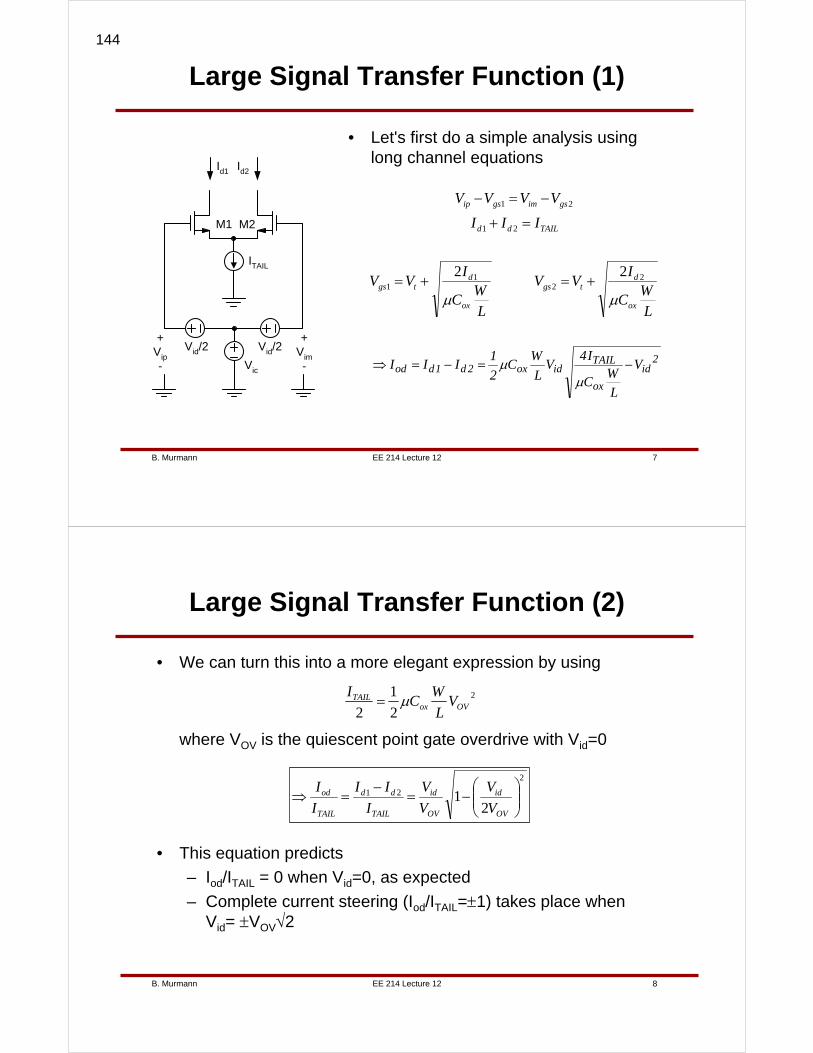
EE 214 Lecture 12B. Murmann 7
Large Signal Transfer Function (1)
• Let's first do a simple analysis using long channel equations
ITAIL
Id1
M1
+Vip-
Id2
Vid/2+
Vim-
Vid/2
Vic
M2
LW
C
IVV
LW
C
IVV
III
VVVV
ox
dtgs
ox
dtgs
TAILdd
gsimgsip
μμ
22
11
21
21
22+=+=
=+
−=−
2id
ox
TAILidox2d1dod V
L
WC
I4V
L
WC
2
1III −=−=⇒
μμ
EE 214 Lecture 12B. Murmann 8
Large Signal Transfer Function (2)
2
21
21 ⎟⎟
⎠
⎞⎜⎜⎝
⎛−=
−=⇒
OV
id
OV
id
TAIL
dd
TAIL
od
V
V
V
V
I
II
I
I
• We can turn this into a more elegant expression by using
2
2
1
2 OVoxTAIL V
L
WC
I μ=
where VOV is the quiescent point gate overdrive with Vid=0
• This equation predicts
– Iod/ITAIL = 0 when Vid=0, as expected
– Complete current steering (Iod/ITAIL=±1) takes place when Vid= ±VOV√2
144
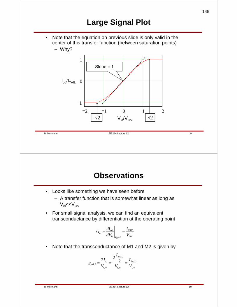
EE 214 Lecture 12B. Murmann 9
Large Signal Plot
• Note that the equation on previous slide is only valid in the center of this transfer function (between saturation points)– Why?
Iod/ITAIL
⎝
2 1 0 1 2
1
0
1
Slope = 1
Vid/VOV-√2 √2
EE 214 Lecture 12B. Murmann 10
Observations
• Looks like something we have seen before
– A transfer function that is somewhat linear as long as Vid<<VOV
• For small signal analysis, we can find an equivalent transconductance by differentiation at the operating point
OV
TAIL
Vid
odm V
I
dV
dIG
id
===0
• Note that the transconductance of M1 and M2 is given by
OV
TAIL
OV
TAIL
OV
D,m V
I
V
I
V
Ig === 2
2221
145
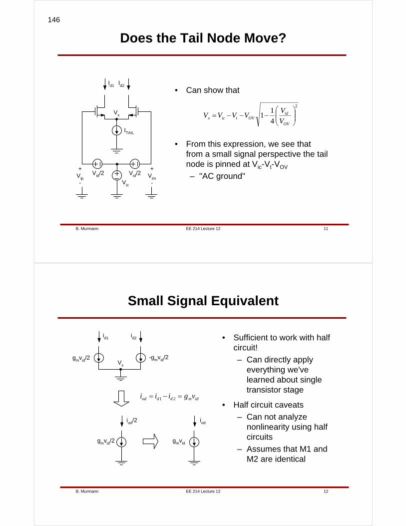
EE 214 Lecture 12B. Murmann 11
Does the Tail Node Move?
• Can show that
ITAIL
Id1
+Vip-
Id2
Vid/2+
Vim-
Vid/2
Vic
Vx
2
4
11 ⎟⎟
⎠
⎞⎜⎜⎝
⎛−−−=
OV
idOVticx V
VVVVV
• From this expression, we see that from a small signal perspective the tail node is pinned at Vic-Vt-VOV
– "AC ground"
EE 214 Lecture 12B. Murmann 12
Small Signal Equivalent
• Sufficient to work with half circuit!
– Can directly apply everything we've learned about single transistor stage
• Half circuit caveats
– Can not analyze nonlinearity using half circuits
– Assumes that M1 and M2 are identical
id1 id2
gmvid/2 Vx
-gmvid/2
iod/2
gmvid/2
iod
gmvid
idmddod vgiii =−= 21
146
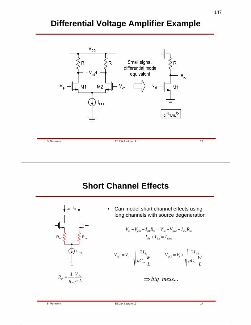
EE 214 Lecture 12B. Murmann 13
Differential Voltage Amplifier Example
EE 214 Lecture 12B. Murmann 14
Short Channel Effects
• Can model short channel effects using long channels with source degeneration
ITAIL
Id1 Id2
Rsx Rsx
LW
C
IVV
LW
C
IVV
III
RIVVRIVV
ox
dtgs
ox
dtgs
TAILdd
sxdgsimsxdgsip
μμ
22
11
21
2211
22+=+=
=+
−−=−−
mess... big⇒L
V
gR
c
OV
msx ε
1=
147

EE 214 Lecture 12B. Murmann 15
Nonlinearity Comparison (1)
• Can look at this using Taylor expansions
• Without Rsx (long channel), we can show that
...V
V
V
V
I
I
OV
id
OV
id
TAIL
od −⎟⎟⎠
⎞⎜⎜⎝
⎛−⎟⎟⎠
⎞⎜⎜⎝
⎛≅
3
8
1
• With Rsx (short channel) this becomes
( ) ( ) ...VRg
V
RgVRg
V
I
I
OVsxm
id
sxmOVsxm
id
TAIL
od −⎟⎟⎠
⎞⎜⎜⎝
⎛⋅+⎟⎟
⎠
⎞⎜⎜⎝
⎛+
−⎟⎟⎠
⎞⎜⎜⎝
⎛⋅+
≅3
11
1
8
1
1
• Short channel differential pair is "more linear"
– But also has less gm at a given current
• For fairness, let's compare nonlinearity at same gm/ID
EE 214 Lecture 12B. Murmann 16
Nonlinearity Comparison (2)
• Recall that
OVsxmD
m
VRgI
g 2
1
1
+≅
• Plugging this into the equations on the previous slide yields
...VI
gV
I
g
I
Iid
D
mid
D
m
TAIL
od −⎟⎟⎠
⎞⎜⎜⎝
⎛−⎟⎟⎠
⎞⎜⎜⎝
⎛≅
3
2
1
8
1
2
1
...VI
g
RgV
I
g
I
Iid
D
m
sxmid
D
m
TAIL
od −⎟⎟⎠
⎞⎜⎜⎝
⎛⎟⎟⎠
⎞⎜⎜⎝
⎛+
−⎟⎟⎠
⎞⎜⎜⎝
⎛≅
3
2
1
1
1
8
1
2
1
Long Channel
Short Channel
• Minor win for short channel in terms of linearity
– In practice, this may be overshadowed by additional effects that are not captured in the simple degeneration model
148
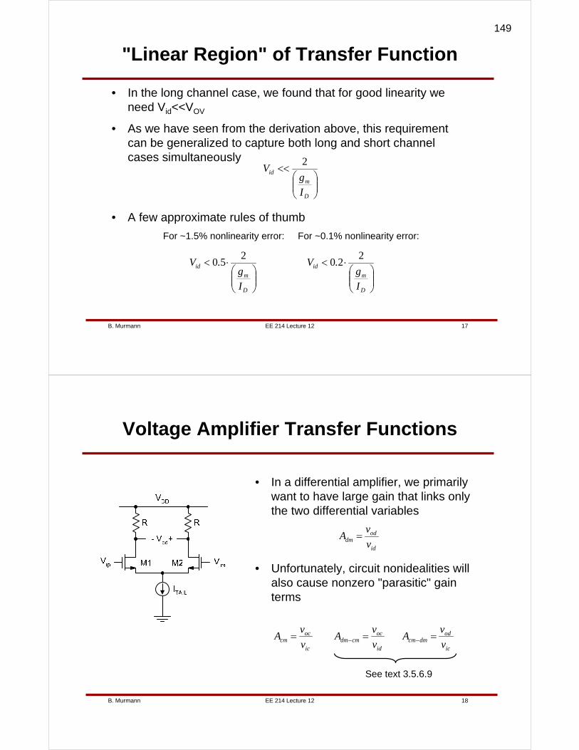
EE 214 Lecture 12B. Murmann 17
"Linear Region" of Transfer Function
• In the long channel case, we found that for good linearity we need Vid<<VOV
• As we have seen from the derivation above, this requirement can be generalized to capture both long and short channel cases simultaneously
• A few approximate rules of thumb
⎟⎟⎠
⎞⎜⎜⎝
⎛<<
D
m
id
Ig
V2
⎟⎟⎠
⎞⎜⎜⎝
⎛⋅<
⎟⎟⎠
⎞⎜⎜⎝
⎛⋅<
D
m
id
D
m
id
Ig
.V
Ig
.V2
202
50
For ~1.5% nonlinearity error: For ~0.1% nonlinearity error:
EE 214 Lecture 12B. Murmann 18
Voltage Amplifier Transfer Functions
• In a differential amplifier, we primarily want to have large gain that links only the two differential variables
id
oddm v
vA =
• Unfortunately, circuit nonidealities will also cause nonzero "parasitic" gain terms
ic
occm v
vA =
id
occmdm v
vA =−
ic
oddmcm v
vA =−
See text 3.5.6.9
149
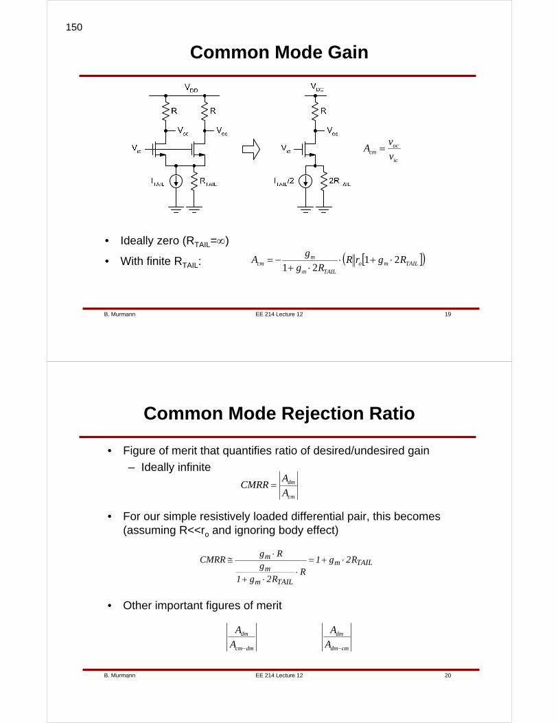
EE 214 Lecture 12B. Murmann 19
Common Mode Gain
• Ideally zero (RTAIL=∞)
• With finite RTAIL:
ic
occm v
vA =
[ ]( )TAILmoTAILm
mcm RgrR
Rg
gA 21
21⋅+⋅
⋅+−=
EE 214 Lecture 12B. Murmann 20
Common Mode Rejection Ratio
• Figure of merit that quantifies ratio of desired/undesired gain
– Ideally infinite
cm
dm
A
ACMRR =
• For our simple resistively loaded differential pair, this becomes (assuming R<<ro and ignoring body effect)
TAILm
TAILm
m
m R2g1R
R2g1
gRg
CMRR ⋅+=⋅
⋅+
⋅≅
• Other important figures of merit
dmcm
dm
A
A
− cmdm
dm
A
A
−
150
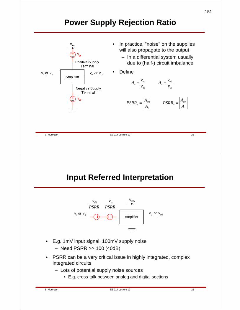
EE 214 Lecture 12B. Murmann 21
Power Supply Rejection Ratio
• In practice, "noise" on the supplies will also propagate to the output
– In a differential system usually due to (half-) circuit imbalance
• Define
dd
od
v
vA =+
ss
od
v
vA =−
++ = A
APSRR dm
−− = A
APSRR dm
EE 214 Lecture 12B. Murmann 22
Input Referred Interpretation
• E.g. 1mV input signal, 100mV supply noise
– Need PSRR >> 100 (40dB)
• PSRR can be a very critical issue in highly integrated, complex integrated circuits
– Lots of potential supply noise sources• E.g. cross-talk between analog and digital sections
Amplifier
VDD
vi or vidvo or vod
+PSRR
vdd
−PSRR
vss
151

EE 214 Lecture 13B. Murmann 1
Lecture 13Current MirrorsOffset Voltage
Boris MurmannStanford University
Copyright © 2007 by Boris Murmann
EE 214 Lecture 13B. Murmann 2
Overview
• Reading
– 4.1, 4.2 (Current Mirrors)
– 3.5.6.6, 3.5.6.7 (Input Offset Voltage)
• References– M. Pelgrom et al., "Matching properties of MOS transistors," IEEE
J. Solid-State Circuits, Oct. 1989.
– P.G. Drennan et al., "Understanding MOSFET mismatch for analog design," IEEE J. Solid-State Circuits, March 2003.
• Introduction
– In this lecture, we will take a closer look at practical implementations of current mirrors with emphasis on high swing biasing techniques. In addition, we will discuss nonidealities such as threshold voltage mismatch and IR drop.
152
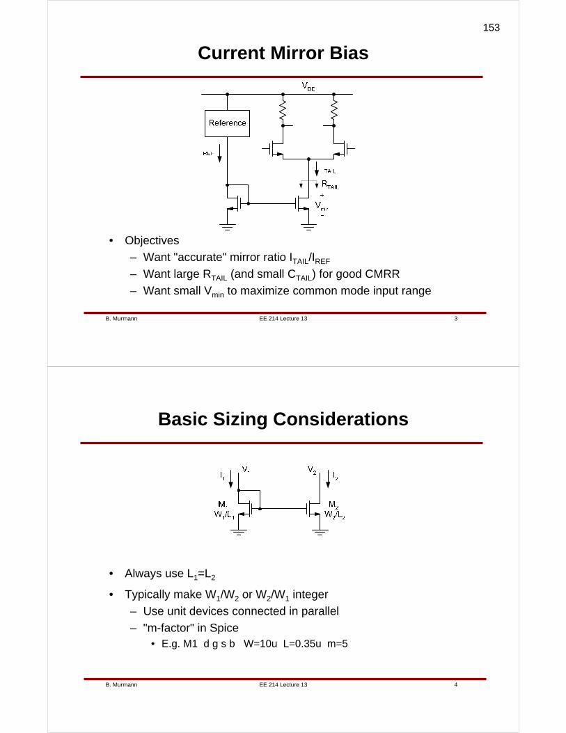
EE 214 Lecture 13B. Murmann 3
Current Mirror Bias
• Objectives
– Want "accurate" mirror ratio ITAIL/IREF
– Want large RTAIL (and small CTAIL) for good CMRR
– Want small Vmin to maximize common mode input range
EE 214 Lecture 13B. Murmann 4
Basic Sizing Considerations
• Always use L1=L2
• Typically make W1/W2 or W2/W1 integer
– Use unit devices connected in parallel
– "m-factor" in Spice• E.g. M1 d g s b W=10u L=0.35u m=5
153
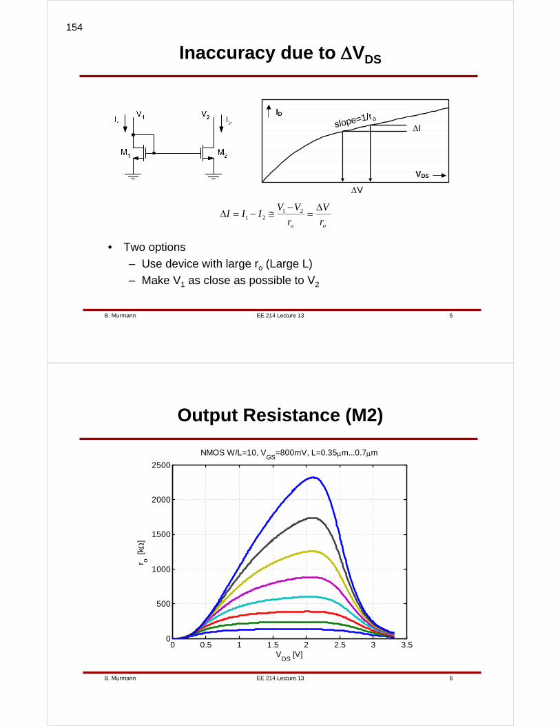
EE 214 Lecture 13B. Murmann 5
Inaccuracy due to ΔVDS
• Two options
– Use device with large ro (Large L)
– Make V1 as close as possible to V2
oo r
V
r
VVIII
Δ=
−≅−=Δ 21
21
VDS
ID
ΔV
ΔIslope=1/ro
EE 214 Lecture 13B. Murmann 6
Output Resistance (M2)
0 0.5 1 1.5 2 2.5 3 3.50
500
1000
1500
2000
2500
NMOS W/L=10, VGS
=800mV, L=0.35μm...0.7μm
VDS
[V]
r o [k Ω
]
154
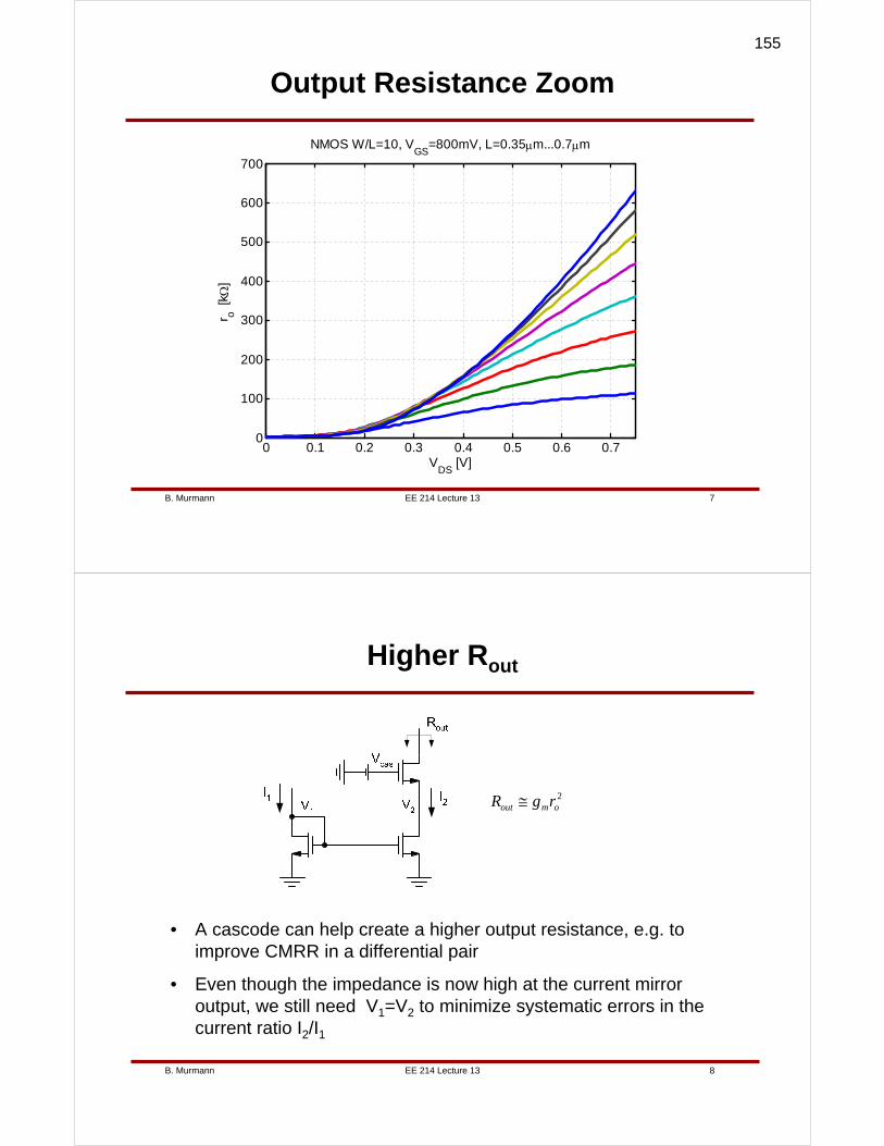
EE 214 Lecture 13B. Murmann 7
Output Resistance Zoom
0 0.1 0.2 0.3 0.4 0.5 0.6 0.70
100
200
300
400
500
600
700
NMOS W/L=10, VGS
=800mV, L=0.35μm...0.7μm
VDS
[V]
r o [k Ω
]
EE 214 Lecture 13B. Murmann 8
Higher Rout
• A cascode can help create a higher output resistance, e.g. to improve CMRR in a differential pair
• Even though the impedance is now high at the current mirror output, we still need V1=V2 to minimize systematic errors in the current ratio I2/I1
2omout rgR ≅
155
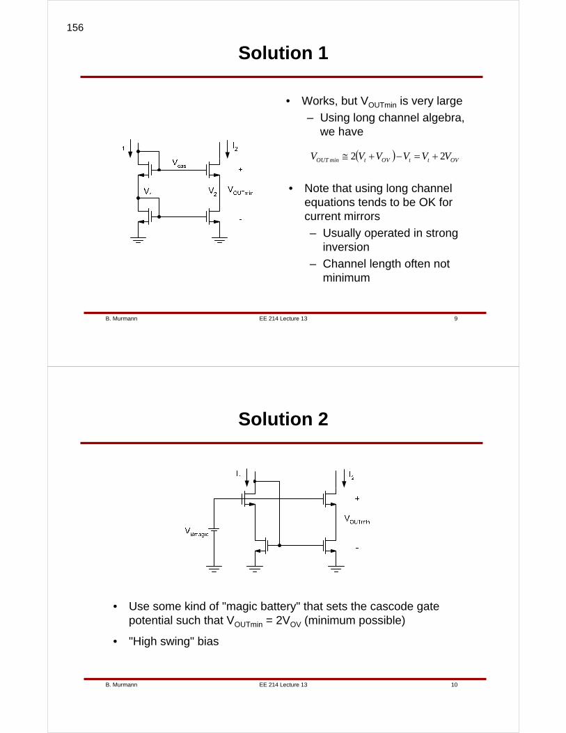
EE 214 Lecture 13B. Murmann 9
Solution 1
• Works, but VOUTmin is very large
– Using long channel algebra, we have
( ) OVttOVtminOUT VVVVVV 22 +=−+≅
• Note that using long channel equations tends to be OK for current mirrors
– Usually operated in strong inversion
– Channel length often not minimum
EE 214 Lecture 13B. Murmann 10
Solution 2
• Use some kind of "magic battery" that sets the cascode gate potential such that VOUTmin = 2VOV (minimum possible)
• "High swing" bias
156

EE 214 Lecture 13B. Murmann 11
Magic Battery 1
• Gate overdrive of ¼ device is twice as large as VOV of all other devices
– Vcas=Vt+2VOV
– VOUTmin = 2VOV
• Sensitive to body effect
EE 214 Lecture 13B. Murmann 12
Magic Battery 2
• Less sensitive to body effect
• Stacked device mimics transistor with length 4L
– May not match characteristics of devices with length L all that well
157
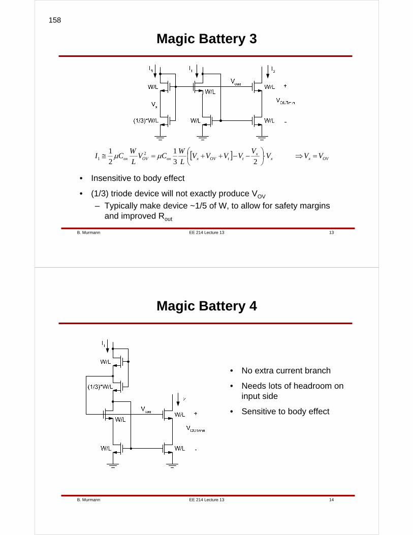
EE 214 Lecture 13B. Murmann 13
Magic Battery 3
• Insensitive to body effect
• (1/3) triode device will not exactly produce VOV
– Typically make device ~1/5 of W, to allow for safety margins and improved Rout
[ ] OVxxx
ttOVxoxOVox VVVV
VVVVL
WCV
L
WCI =⇒⋅⎟
⎠⎞
⎜⎝⎛ −−++=≅
23
1
2
1 21 μμ
EE 214 Lecture 13B. Murmann 14
Magic Battery 4
• No extra current branch
• Needs lots of headroom on input side
• Sensitive to body effect
158

EE 214 Lecture 13B. Murmann 15
Magic Battery 5
• The previous circuits assumed that Lmirror=Lcascode
– Sometimes want Lmirror≠Lcascode
• The above circuit makes Vcas =Vt2 + VOV2 + VOV1
– VOUTmin becomes VOV2 + VOV1, as desired
I2I1
W1/L1 W1/L1
VcasW2/L2
W2/L2
I1
(2/3)*W1/L1
W1/L1
Vx
I1
W2/L2
EE 214 Lecture 13B. Murmann 16
Design Considerations
• In all of the above-discussed circuits, care must be taken to keep the devices in their active region with sufficient safety margin, and not to "waste" too much ro
– Typically use ~1/6 in 1/4 size device approach (slide 10)
– Typically use ~1/5 in 1/3 triode device approach (slides 12-14)
• Work with integer ratios and unit devices as much as possible
– Using a 1/5 device really means that we work with a unit device of size 1, and use 5 of them elsewhere
• Sometimes desirable to keep mirror ratio (I2/I1) reasonably small
– Say, no larger than 10…20
– Ensures reasonable bandwidth at bias nodes for fast recovery from noise coupling
159
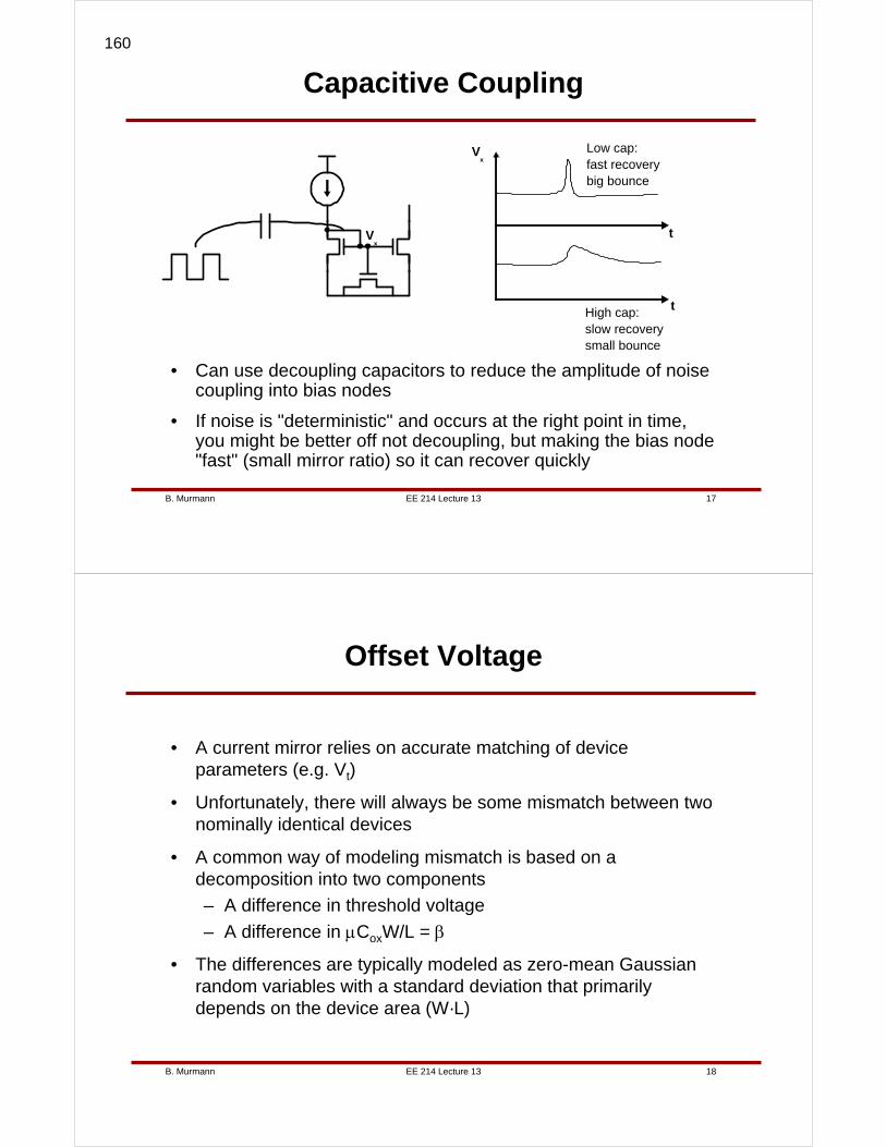
EE 214 Lecture 13B. Murmann 17
Capacitive Coupling
• Can use decoupling capacitors to reduce the amplitude of noise coupling into bias nodes
• If noise is "deterministic" and occurs at the right point in time, you might be better off not decoupling, but making the bias node"fast" (small mirror ratio) so it can recover quickly
Vx
Low cap:fast recovery
High cap:slow recovery
big bounce
small bounce
t
t
Vx
EE 214 Lecture 13B. Murmann 18
Offset Voltage
• A current mirror relies on accurate matching of device parameters (e.g. Vt)
• Unfortunately, there will always be some mismatch between two nominally identical devices
• A common way of modeling mismatch is based on a decomposition into two components
– A difference in threshold voltage
– A difference in μCoxW/L = β
• The differences are typically modeled as zero-mean Gaussian random variables with a standard deviation that primarily depends on the device area (W·L)
160

EE 214 Lecture 13B. Murmann 19
Pelgrom Coefficients
• In 0.35μm technology: AVt ≅ 7mV-μm, Aβ ≅ 1%-μm
– AVt tends to scale down with technology, roughly proportional to gate oxide thickness
– Aβ has remained roughly constant with scaling
• Example: W=10μm, L=0.35μm
WL
A
WL
At
t
VV
β
ββσσ == ΔΔ
%53.05.3
%1mV7.3
5.3
mV7tV ====
ββΔΔ σσ
EE 214 Lecture 13B. Murmann 20
Inaccuracy Due to Mismatch
βΔΔΔ 1tm21 IVgIII +≅−=
βΔΔΔ+≅ t
1
m
1V
I
g
I
I
( ) ( ) ( ) %74.3%53.0%7.3%53.0mV7.3A
S10 222
2
I
I
1
=+=+⎟⎠⎞
⎜⎝⎛ ⋅=Δσ
• Example: W=10μm, L=0.35μm, gm/ID=10S/A
• Threshold mismatch usually dominates
161
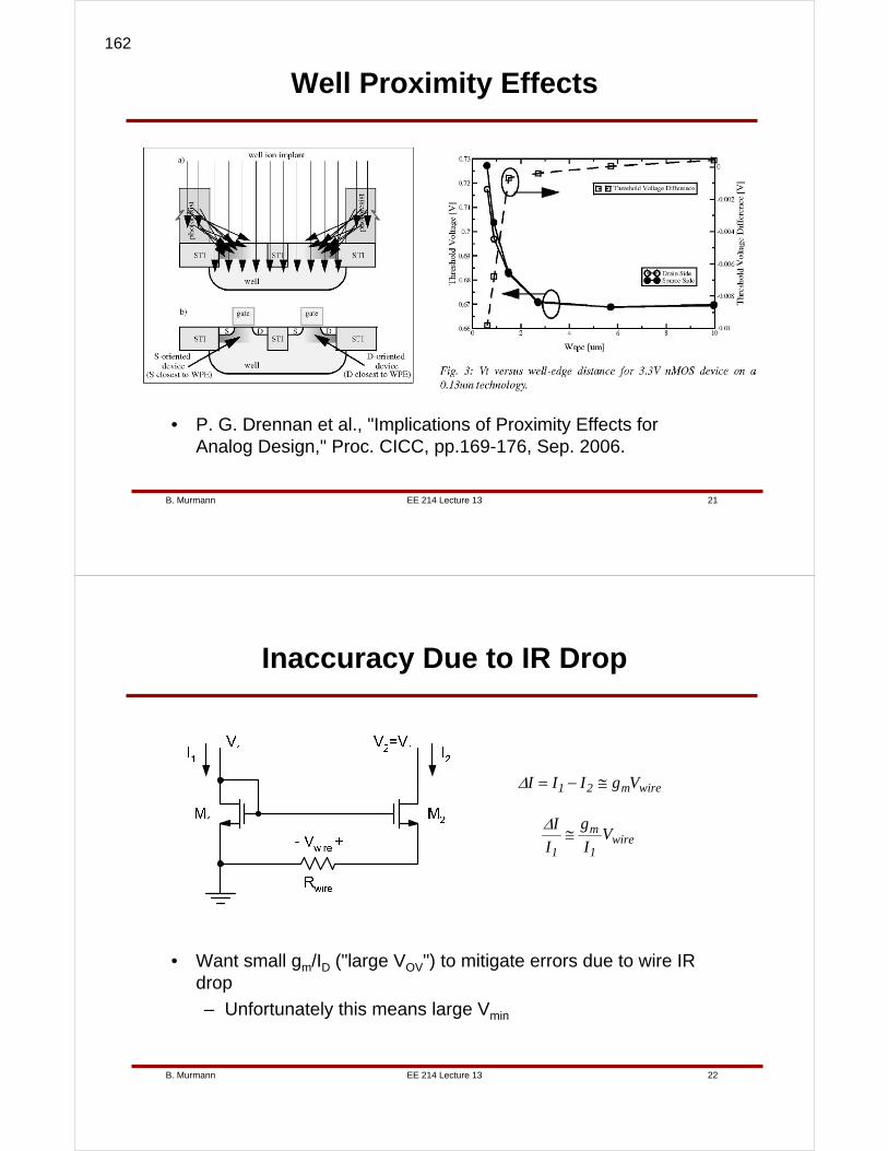
EE 214 Lecture 13B. Murmann 21
Well Proximity Effects
• P. G. Drennan et al., "Implications of Proximity Effects for Analog Design," Proc. CICC, pp.169-176, Sep. 2006.
EE 214 Lecture 13B. Murmann 22
Inaccuracy Due to IR Drop
• Want small gm/ID ("large VOV") to mitigate errors due to wire IR drop
– Unfortunately this means large Vmin
wirem21 VgIII ≅−=Δ
wire1
m
1V
I
g
I
I≅
Δ
162

EE 214 Lecture 13B. Murmann 23
A Note on Current Mirror Accuracy
• As we have seen, it is very hard to build "highly" accurate current mirrors– Systematic errors: ΔVDS, IR Drop, …– Random errors: ΔVt, …
• This is often not an issue– E.g. gm ~ sqrt(ID); 20% error in ID causes ~10% error in gm
• For mirrors using short channels, it is sometimes OK to tweak the mirror ratio to compensate for ΔVDS-induced systematic errors– Keep in mind that you should not overdo this; it makes no
sense to tweak a mirror in Spice to unrealistic accuracies– Tweaking is only going to work in practice if you know that
gds is properly modeled in your technology file• Not always the case
EE 214 Lecture 13B. Murmann 24
Current Distribution (1)
• Typically, we'll only have one single reference current generator on a chip
• Can generate/distribute currents across chip in two different ways
– Distribute gate voltage• Can cause big problems due to IR drop and process gradients
• Usually limited to local distribution
– Distribute currents• Have one global bias cell close to reference that sends currents
into local biasing sub-circuits
• Disadvantage: consumes additional current
163
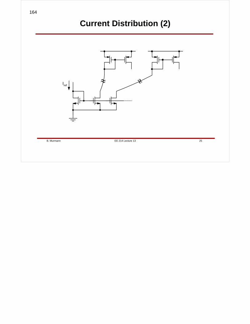
EE 214 Lecture 13B. Murmann 25
Current Distribution (2)
Iref
164
EE 214 Lecture 14B. Murmann 1
Lecture 14Process Variations
Feedback
Boris MurmannStanford University
Copyright © 2007 by Boris Murmann
EE 214 Lecture 14B. Murmann 2
Overview
• Reading
– 8.0, 8.1, 8.2, 8.3 (Feedback)
– 9.2 (Relation Between Gain and Bandwidth)
– Supplementary Handout "Feedback Systems" by Tom Lee (see web, optional)
• Introduction
– In today's lecture we will first take a look at typical component variations in CMOS technology. In light of these numbers, we then consider negative feedback as a tool for building amplifiers with precisely defined gain. As we shall see, using a forward amplifier with "high", but arbitrary gain, combined with a ratiometric, passive feedback network allows us to build drift and process insensitive precision gain stages.
165
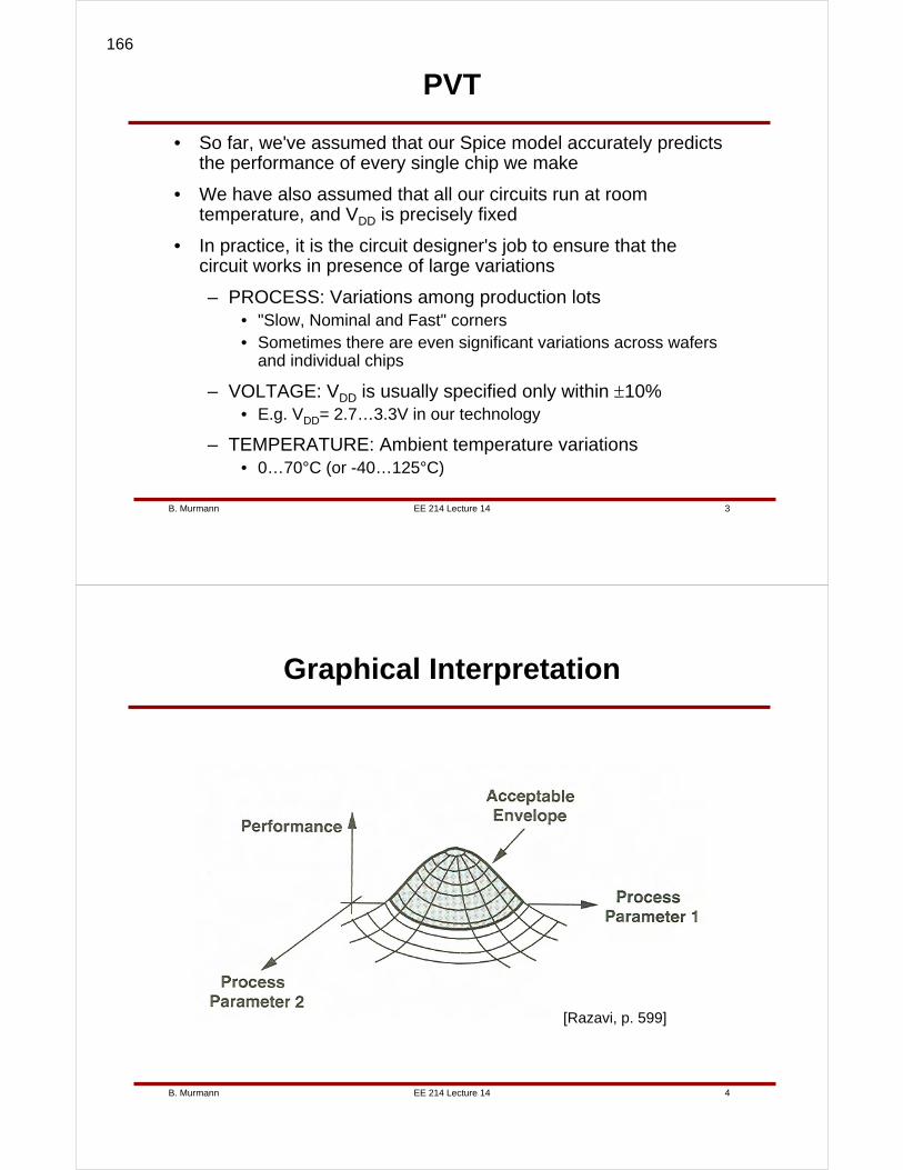
EE 214 Lecture 14B. Murmann 3
PVT
• So far, we've assumed that our Spice model accurately predicts the performance of every single chip we make
• We have also assumed that all our circuits run at room temperature, and VDD is precisely fixed
• In practice, it is the circuit designer's job to ensure that thecircuit works in presence of large variations
– PROCESS: Variations among production lots• "Slow, Nominal and Fast" corners• Sometimes there are even significant variations across wafers
and individual chips
– VOLTAGE: VDD is usually specified only within ±10%• E.g. VDD= 2.7…3.3V in our technology
– TEMPERATURE: Ambient temperature variations• 0…70°C (or -40…125°C)
EE 214 Lecture 14B. Murmann 4
Graphical Interpretation
[Razavi, p. 599]
166
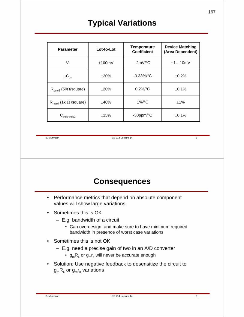
EE 214 Lecture 14B. Murmann 5
Typical Variations
±0.1%0.2%/°C±20%Rpoly2 (50Ω/square)
±1%1%/°C±40%Rnwell (1k Ω /square)
±0.1%-30ppm/°C±15%Cpoly-poly2
±0.2%-0.33%/°C±20%μCox
~1…10mV-2mV/°C±100mVVt
Device Matching (Area Dependent)
Temperature Coefficient
Lot-to-LotParameter
EE 214 Lecture 14B. Murmann 6
Consequences
• Performance metrics that depend on absolute component values will show large variations
• Sometimes this is OK
– E.g. bandwidth of a circuit• Can overdesign, and make sure to have minimum required
bandwidth in presence of worst case variations
• Sometimes this is not OK
– E.g. need a precise gain of two in an A/D converter• gmRL or gmro will never be accurate enough
• Solution: Use negative feedback to desensitize the circuit to gmRL or gmro variations
167
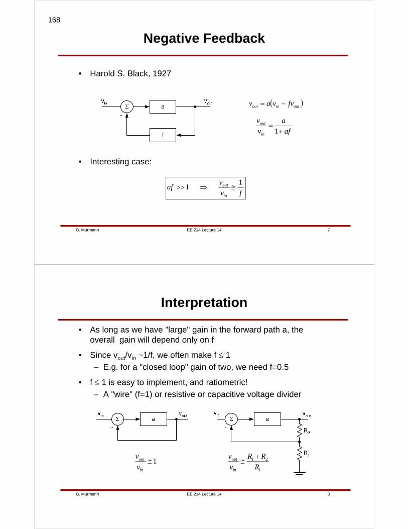
EE 214 Lecture 14B. Murmann 7
Negative Feedback
• Harold S. Black, 1927
( )outinout fvvav −=
af
a
v
v
in
out
+=
1
• Interesting case:
fv
vaf
in
out 11 ≅⇒>>
EE 214 Lecture 14B. Murmann 8
Interpretation
• As long as we have "large" gain in the forward path a, the overall gain will depend only on f
• Since vout/vin ~1/f, we often make f ≤ 1
– E.g. for a "closed loop" gain of two, we need f=0.5
• f ≤ 1 is easy to implement, and ratiometric!
– A "wire" (f=1) or resistive or capacitive voltage divider
1≅in
out
v
v
1
21
R
RR
v
v
in
out +≅
168
EE 214 Lecture 14B. Murmann 9
Example
• Case 2: a=1000
5021 .fRR =⇒=
• Case 1: a=100
.....f
av
v
in
out 96078150
1001
11
1=
+=
+=
.....f
av
v
in
out 996007150
10001
11
1=
+=
+=
• 10x variation in forward gain, and only about 1.8% change in closed loop gain!
EE 214 Lecture 14B. Murmann 10
Gain Sensitivity
• Defineaf
aA
+=
1
• Can show that
Taa
afaa
A
A
+
Δ
=+
Δ
=Δ
11
• Fractional change in gain is reduced by product of a and f, which can be made arbitrarily large (conceptually)
– Loop gain T
• We will find that loop gain is a very meaningful parameter that will also appear in bandwidth and impedance calculations
– More later…
169
EE 214 Lecture 14B. Murmann 11
Effect of Negative Feedback on Nonlinearity
• Substitute (2) into (1), then compare coefficients to get
( ) ( ) ( )
( ) 331
331
2
1
inin
!
out
outinoutinout
vbvbv
fvvafvvav
+=
−+−=
( )41
33
1
11
11 fa
ab
fa
ab
+=
+=
• Linear term as expected, reduced by (1+T)
• Cubic term reduced by (1+T)4!
EE 214 Lecture 14B. Murmann 12
Negative Feedback and Bandwidth
• Closed loop transfer function:
1
0
1ps
a)s(a.g.E
−=
fapsfa
a
f)s(a
)s(a)s(A
01
0
0
11
1
1
11+
−⋅
+=
+=
• Bandwidth increases by (1+T)!
– But gain is reduced by (1+T)
• Product of gain and bandwidth remains constant
170
EE 214 Lecture 14B. Murmann 13
Bode Plot Illustration
EE 214 Lecture 14B. Murmann 14
Early Obstacles
• Today we are taking the concept of negative feedback for granted
• At the time of his "invention," Harold Black had a hard time convincing his colleagues that negative feedback was indeed something useful
– It was very hard to make a "high gain" forward amplifier using vacuum tubes
– Why have large gain and then throw it away by applying negative feedback?
• Long before negative feedback had been deemed useful, positive feedback was routinely applied to increase the gain of amplifiers
171
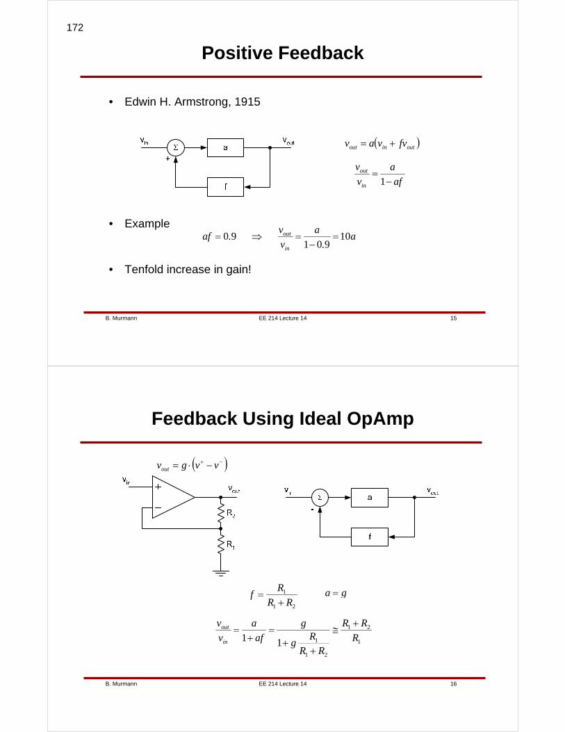
EE 214 Lecture 14B. Murmann 15
Positive Feedback
• Edwin H. Armstrong, 1915
( )outinout fvvav +=
af
a
v
v
in
out
−=
1
• Examplea
.
a
v
v.af
in
out 10901
90 =−
=⇒=
• Tenfold increase in gain!
EE 214 Lecture 14B. Murmann 16
Feedback Using Ideal OpAmp
21
1
RR
Rf
+=
( )−+ −⋅= vvgvout
1
21
21
111 R
RR
RRR
g
g
af
a
v
v
in
out +≅
++
=+
=
ga =
172
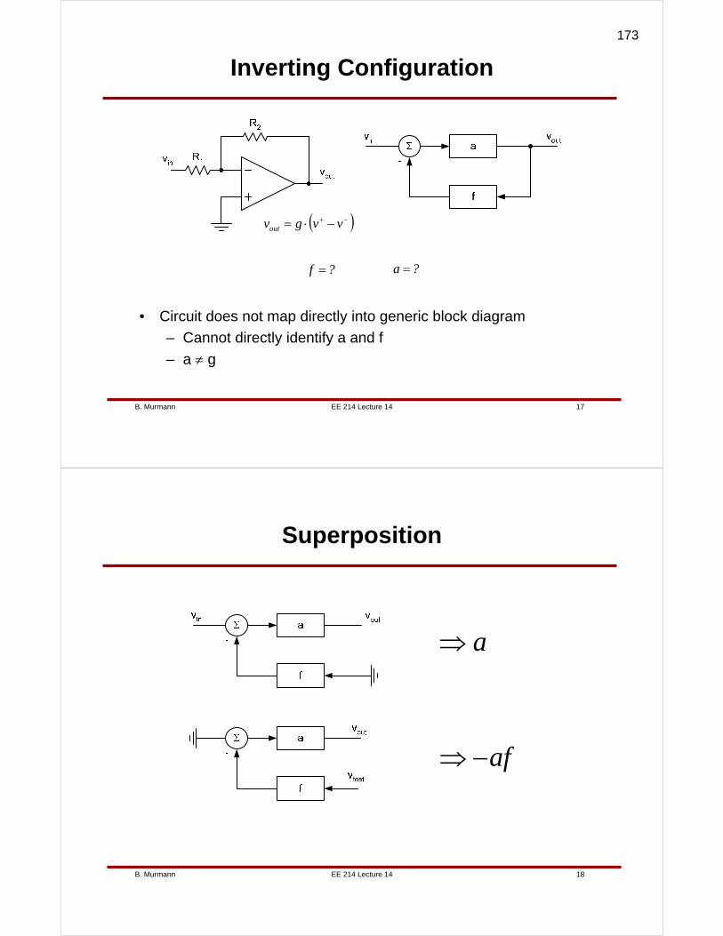
EE 214 Lecture 14B. Murmann 17
Inverting Configuration
• Circuit does not map directly into generic block diagram
– Cannot directly identify a and f
– a ≠ g
?f =
( )−+ −⋅= vvgvout
?a =
EE 214 Lecture 14B. Murmann 18
Superposition
a⇒
af−⇒
173
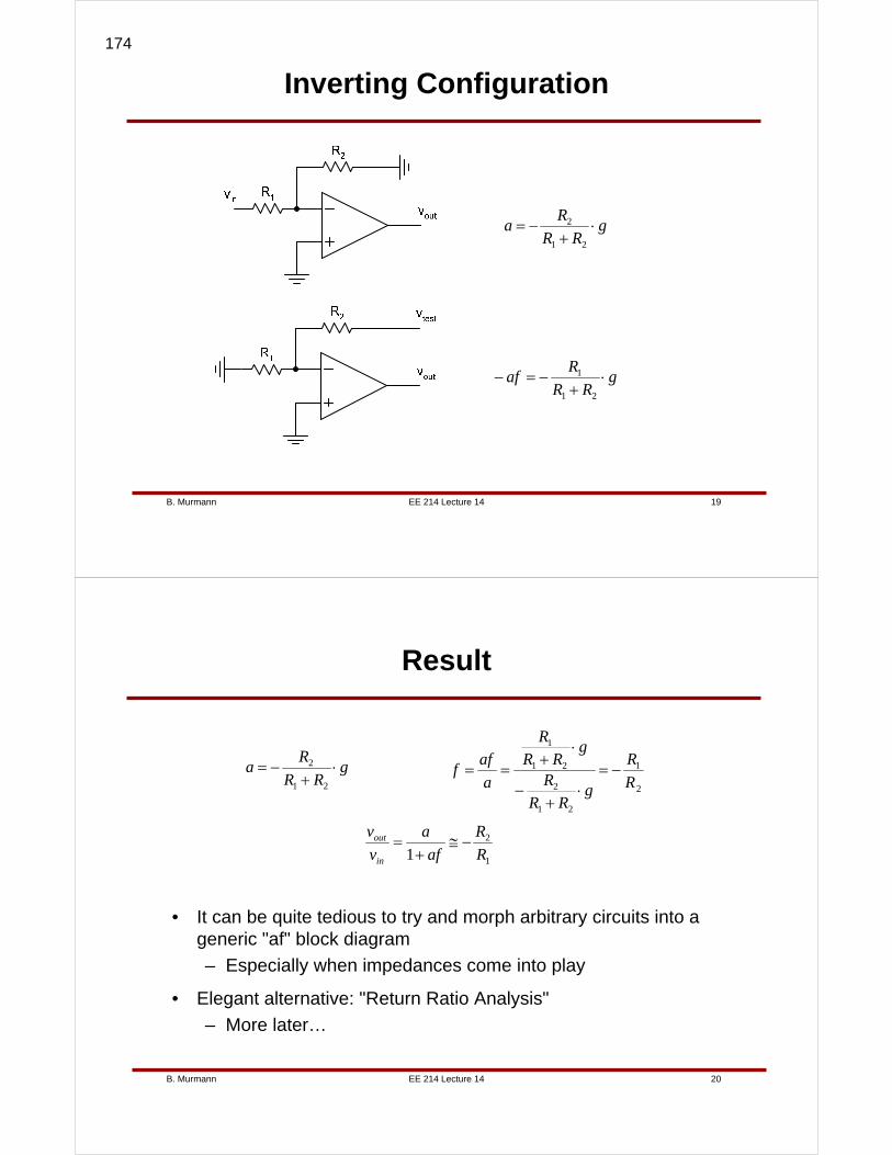
EE 214 Lecture 14B. Murmann 19
Inverting Configuration
gRR
Ra ⋅
+−=
21
2
gRR
Raf ⋅
+−=−
21
1
EE 214 Lecture 14B. Murmann 20
Result
2
1
21
2
21
1
R
R
gRR
R
gRR
R
a
aff −=
⋅+
−
⋅+
==gRR
Ra ⋅
+−=
21
2
1
2
1 R
R
af
a
v
v
in
out −≅+
=
• It can be quite tedious to try and morph arbitrary circuits into a generic "af" block diagram
– Especially when impedances come into play
• Elegant alternative: "Return Ratio Analysis"
– More later…
174
EE 214 Lecture 15B. Murmann 1
Lecture 15Fully Differential AmplifiersSwitched-Capacitor Circuits
Boris MurmannStanford University
Copyright © 2007 by Boris Murmann
EE 214 Lecture 15B. Murmann 2
Overview
• Reading– 6.0, 6.1.1, 6.1.2, 6.1.2 (Basic Feedback Concepts)– 12.1, 12.2, 12.3, 12.4 (Fully Differential OpAmps)– 6.1.7 (Internal Amplifiers)
• Introduction– Having discussed the basic properties of ideal feedback loops, we
will now take steps toward a practical implementation of feedback amplifiers in CMOS technology. The first amplifier we consider uses a very crude gain stage, composed of a simple differential pair and an active current mirror load. For the time being, we will use this simple topology as a vehicle to gain basic insight into terminology, analysis and design tradeoffs.
– As we will argue, it is generally difficult to drive resistive loads with an amplifier, as the load tends to reduce the circuit's gain. As a result, many "internal amplifiers" in integrated circuits are based on purely capacitive feedback, using a "switched-capacitor" approach.
175

EE 214 Lecture 15B. Murmann 3
A Crude "High-Gain" Amplifier
• Output common mode not well defined
– Depends on mismatch in currents between top and bottom current mirror
EE 214 Lecture 15B. Murmann 4
Common Mode Feedback (1)
• Feedback loop forces Voc=Voc,desired by adjusting tail current
MPa,b
IctrlMNT
176
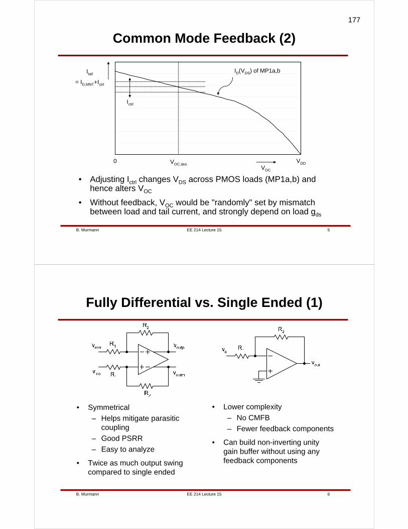
EE 214 Lecture 15B. Murmann 5
Common Mode Feedback (2)
• Adjusting Ictrl changes VDS across PMOS loads (MP1a,b) and hence alters VOC
• Without feedback, VOC would be "randomly" set by mismatch between load and tail current, and strongly depend on load gds
ID(VDS) of MP1a,b
VOC
VDD0 VOC,des
Itail
= ID,MNT+Ictrl
Ictrl
EE 214 Lecture 15B. Murmann 6
Fully Differential vs. Single Ended (1)
• Symmetrical
– Helps mitigate parasitic coupling
– Good PSRR
– Easy to analyze
• Twice as much output swing compared to single ended
• Lower complexity
– No CMFB
– Fewer feedback components
• Can build non-inverting unity gain buffer without using any feedback components
177
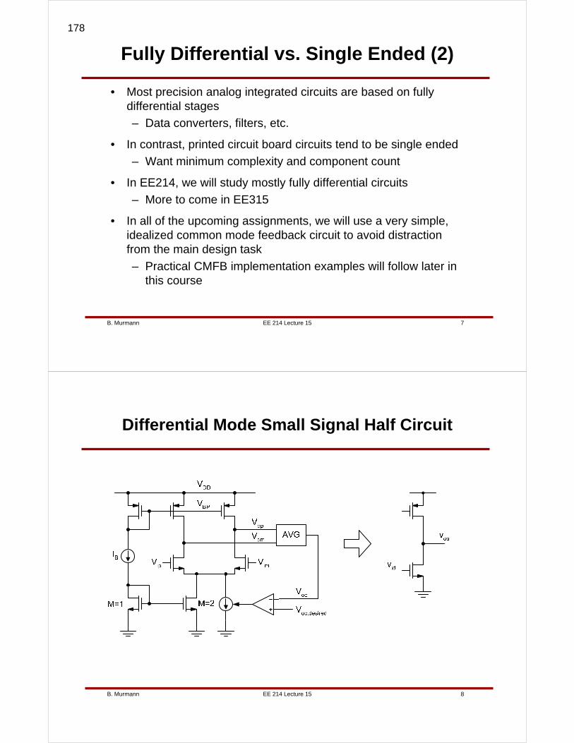
EE 214 Lecture 15B. Murmann 7
Fully Differential vs. Single Ended (2)
• Most precision analog integrated circuits are based on fully differential stages
– Data converters, filters, etc.
• In contrast, printed circuit board circuits tend to be single ended
– Want minimum complexity and component count
• In EE214, we will study mostly fully differential circuits
– More to come in EE315
• In all of the upcoming assignments, we will use a very simple, idealized common mode feedback circuit to avoid distraction from the main design task
– Practical CMFB implementation examples will follow later in this course
EE 214 Lecture 15B. Murmann 8
Differential Mode Small Signal Half Circuit
178
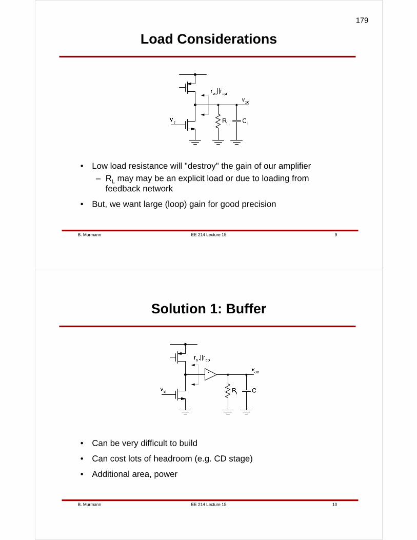
EE 214 Lecture 15B. Murmann 9
Load Considerations
• Low load resistance will "destroy" the gain of our amplifier
– RL may may be an explicit load or due to loading from feedback network
• But, we want large (loop) gain for good precision
EE 214 Lecture 15B. Murmann 10
Solution 1: Buffer
• Can be very difficult to build
• Can cost lots of headroom (e.g. CD stage)
• Additional area, power
179
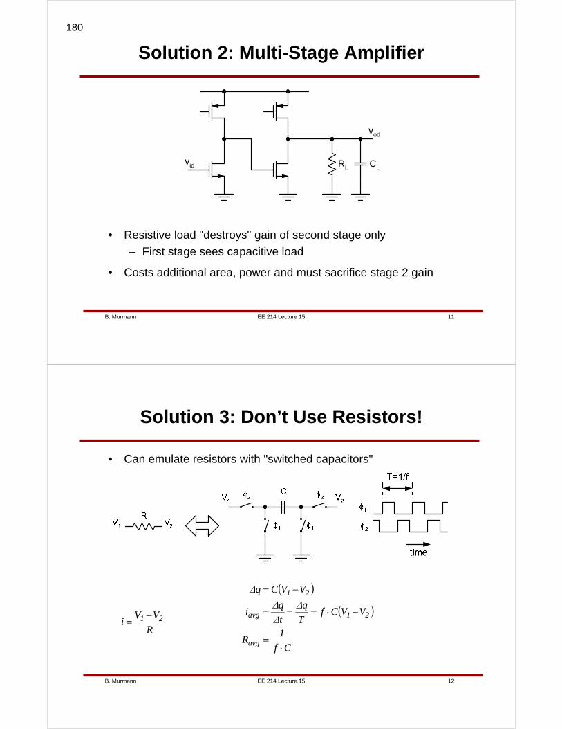
EE 214 Lecture 15B. Murmann 11
Solution 2: Multi-Stage Amplifier
• Resistive load "destroys" gain of second stage only
– First stage sees capacitive load
• Costs additional area, power and must sacrifice stage 2 gain
vid
vod
RL CL
EE 214 Lecture 15B. Murmann 12
Solution 3: Don’t Use Resistors!
• Can emulate resistors with "switched capacitors"
( )
( )
Cf
1R
VVCfT
q
t
qi
VVCq
avg
21avg
21
⋅=
−⋅===
−=Δ
ΔΔ
Δ
R
VVi 21 −=
180
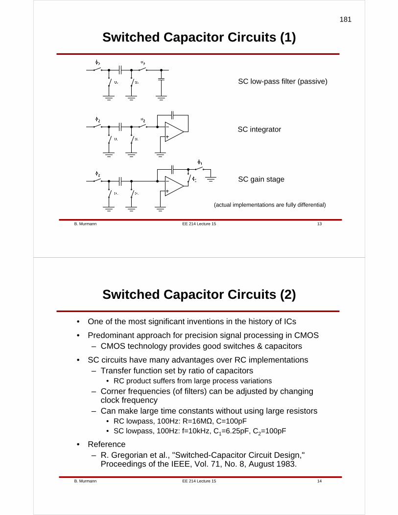
EE 214 Lecture 15B. Murmann 13
Switched Capacitor Circuits (1)
SC low-pass filter (passive)
SC integrator
SC gain stage
(actual implementations are fully differential)
EE 214 Lecture 15B. Murmann 14
Switched Capacitor Circuits (2)
• One of the most significant inventions in the history of ICs
• Predominant approach for precision signal processing in CMOS– CMOS technology provides good switches & capacitors
• SC circuits have many advantages over RC implementations– Transfer function set by ratio of capacitors
• RC product suffers from large process variations
– Corner frequencies (of filters) can be adjusted by changing clock frequency
– Can make large time constants without using large resistors• RC lowpass, 100Hz: R=16MΩ, C=100pF • SC lowpass, 100Hz: f=10kHz, C1=6.25pF, C2=100pF
• Reference– R. Gregorian et al., "Switched-Capacitor Circuit Design,"
Proceedings of the IEEE, Vol. 71, No. 8, August 1983.
181
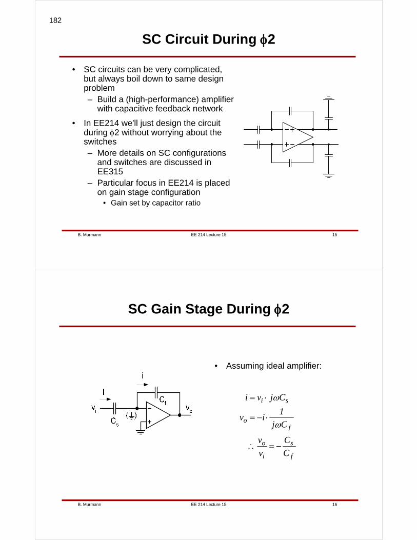
EE 214 Lecture 15B. Murmann 15
SC Circuit During φ2
• SC circuits can be very complicated, but always boil down to same design problem– Build a (high-performance) amplifier
with capacitive feedback network
• In EE214 we'll just design the circuit during φ2 without worrying about the switches– More details on SC configurations
and switches are discussed in EE315
– Particular focus in EE214 is placed on gain stage configuration
• Gain set by capacitor ratio
EE 214 Lecture 15B. Murmann 16
SC Gain Stage During φ2
f
s
i
o
fo
si
C
C
v
v
Cj
1iv
Cjvi
−=∴
⋅−=
⋅=
ω
ω
• Assuming ideal amplifier:
182

EE 214 Lecture 15B. Murmann 17
Noise in SC Gain Stage (1)
• Output is usually sampled by another switched capacitor stage
• What is the relevant noise bandwidth?
EE 214 Lecture 15B. Murmann 18
Noise in SC Gain Stage (2)
• From Parseval's theorem, it follows that the noise power of the output samples is equal to the power spectral density of Vo (during φ2) integrated over all frequencies
– Total integrated noise as discussed in lecture 9
• The dynamic range of the circuit is thus given by:
– We'll derive expressions for different types of amplifiers in lecture 19
∫∞
⋅
=
0
2o,n
2max,peak,o
dff
v
V21
DR
Δ
183
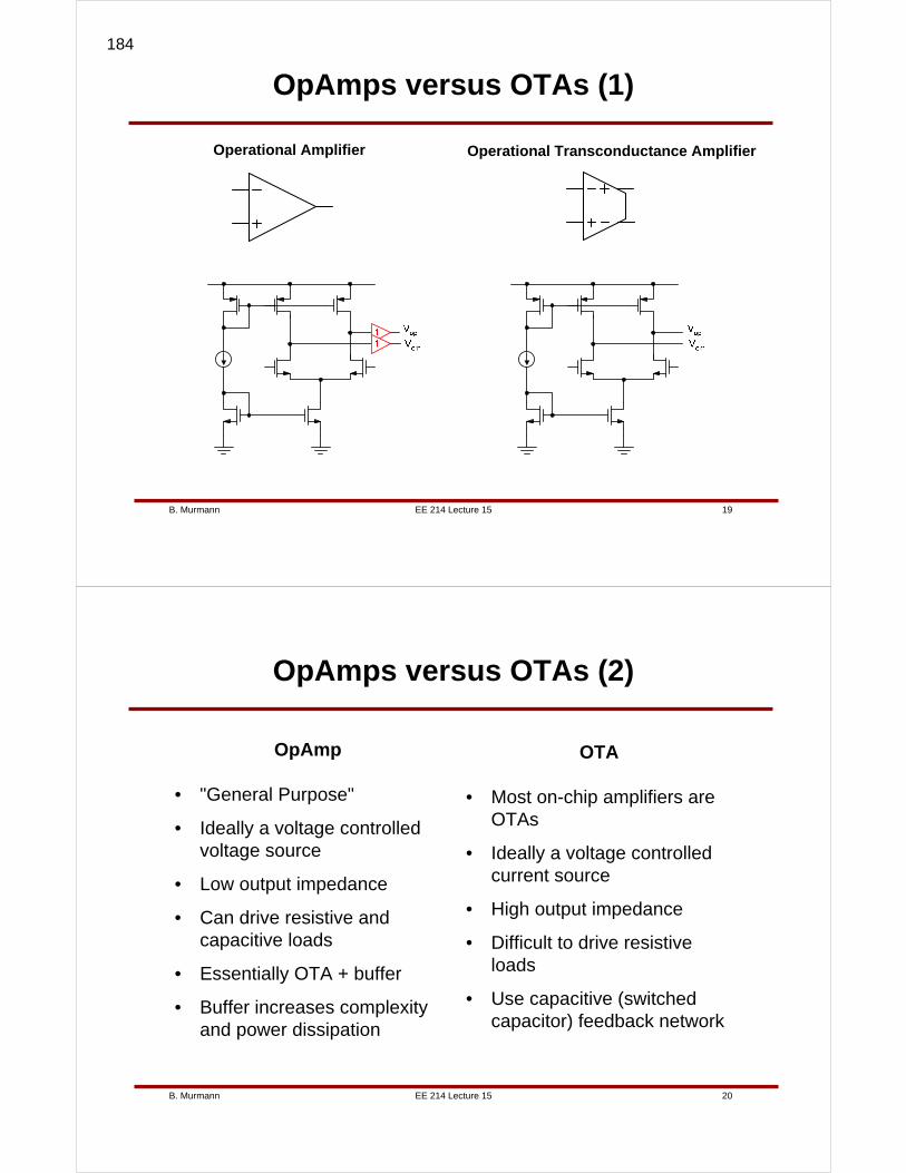
EE 214 Lecture 15B. Murmann 19
OpAmps versus OTAs (1)
Operational Amplifier Operational Transconductance Amplifier
EE 214 Lecture 15B. Murmann 20
OpAmps versus OTAs (2)
OpAmp
• "General Purpose"
• Ideally a voltage controlled voltage source
• Low output impedance
• Can drive resistive and capacitive loads
• Essentially OTA + buffer
• Buffer increases complexity and power dissipation
OTA
• Most on-chip amplifiers are OTAs
• Ideally a voltage controlled current source
• High output impedance
• Difficult to drive resistive loads
• Use capacitive (switched capacitor) feedback network
184

EE 214 Lecture 16B. Murmann 1
Lecture 16
StabilityAnalysis of Feedback Circuits
Boris MurmannStanford University
Copyright © 2007 by Boris Murmann
EE 214 Lecture 16B. Murmann 2
Overview
• Reading
– 9.3 (Stability)
– 8.8 (Return Ratio Analysis)
– Supplementary Handout "Feedback Systems" by Tom Lee (see web, optional)
• Introduction
– This lecture covers basics on the analysis of feedback amplifiers. Using a simple OTA with capacitive feedback as an example, we will study the so called "Return Ratio" method as a tool to assess stability and calculate the bandwidth of feedback amplifiers. Interestingly, most relevant performance metrics follow directly from the "return ratio" or loop gain of the circuit, which highlights the significance of this parameter in feedback system design.
185

EE 214 Lecture 16B. Murmann 3
Stability
• Most general criterion: BIBO
– Bounded input – bounded output
– Applies to any system
• A continuous time linear system is BIBO stable if all its poles are in the left half of the s-plane
– Can calculate roots of 1+T(s) to check stability• Tedious and hard to do in general
)s(T
)s(a
)s(f)s(a
)s(a
v
v)s(A
i
o
+=
+==
11
EE 214 Lecture 16B. Murmann 4
Methods for Checking Stability
• Nyquist Criterion
– Based on evaluating T(s) in a polar plot
– Works for arbitrary T(s)• Even if T(s) itself is unstable
– See books on control theory for details, or e.g.• N. M. Nguyen and R. G. Meyer, "Start-up and Frequency Stability in
High-Frequency Oscillators," IEEE JSSC, pp. 810-820, May 1992.
• Bode Criterion
– A subset of the general Nyquist criterion that can be applied when T(s) itself is stable
• Safe to use in most electronic circuits
• Beware of exceptions
– System is unstable when |T(jω)| > 1 at the frequency where Phase(T(jω)) = -180°
– Can use simple bode plot to check for stability
186
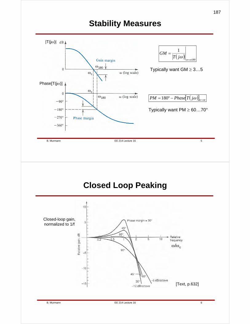
EE 214 Lecture 16B. Murmann 5
Stability Measures
ωc
ω180
ωc
ω180
|T(jω)|
Phase[T(jω)]
( )[ ] cjTPhasePM ωωω =−°=180
( )180
1
ωωω
=
=jT
GM
Typically want GM ≥ 3…5
Typically want PM ≥ 60…70°
EE 214 Lecture 16B. Murmann 6
Closed Loop Peaking
ω/ωc
[Text, p.632]
Closed-loop gain, normalized to 1/f
187
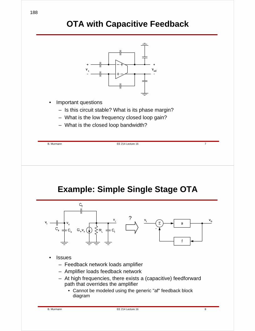
EE 214 Lecture 16B. Murmann 7
OTA with Capacitive Feedback
• Important questions
– Is this circuit stable? What is its phase margin?
– What is the low frequency closed loop gain?
– What is the closed loop bandwidth?
EE 214 Lecture 16B. Murmann 8
Example: Simple Single Stage OTA
• Issues– Feedback network loads amplifier– Amplifier loads feedback network– At high frequencies, there exists a (capacitive) feedforward
path that overrides the amplifier• Cannot be modeled using the generic "af" feedback block
diagram
?
188
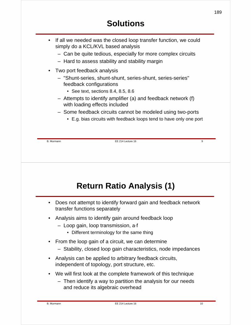
EE 214 Lecture 16B. Murmann 9
Solutions
• If all we needed was the closed loop transfer function, we couldsimply do a KCL/KVL based analysis
– Can be quite tedious, especially for more complex circuits
– Hard to assess stability and stability margin
• Two port feedback analysis
– "Shunt-series, shunt-shunt, series-shunt, series-series" feedback configurations
• See text, sections 8.4, 8.5, 8.6
– Attempts to identify amplifier (a) and feedback network (f) with loading effects included
– Some feedback circuits cannot be modeled using two-ports• E.g. bias circuits with feedback loops tend to have only one port
EE 214 Lecture 16B. Murmann 10
Return Ratio Analysis (1)
• Does not attempt to identify forward gain and feedback network transfer functions separately
• Analysis aims to identify gain around feedback loop
– Loop gain, loop transmission, a·f• Different terminology for the same thing
• From the loop gain of a circuit, we can determine
– Stability, closed loop gain characteristics, node impedances
• Analysis can be applied to arbitrary feedback circuits, independent of topology, port structure, etc.
• We will first look at the complete framework of this technique
– Then identify a way to partition the analysis for our needs and reduce its algebraic overhead
189
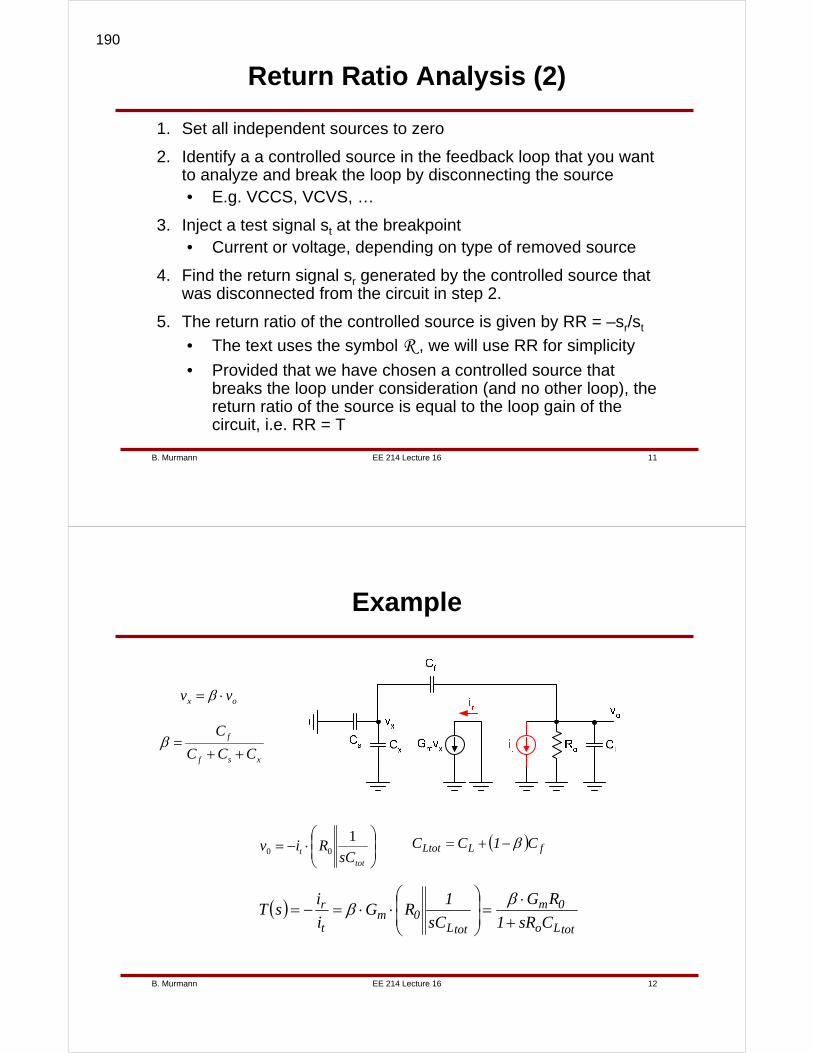
EE 214 Lecture 16B. Murmann 11
Return Ratio Analysis (2)
1. Set all independent sources to zero
2. Identify a a controlled source in the feedback loop that you want to analyze and break the loop by disconnecting the source• E.g. VCCS, VCVS, …
3. Inject a test signal st at the breakpoint• Current or voltage, depending on type of removed source
4. Find the return signal sr generated by the controlled source that was disconnected from the circuit in step 2.
5. The return ratio of the controlled source is given by RR = –sr/st
• The text uses the symbol R , we will use RR for simplicity
• Provided that we have chosen a controlled source that breaks the loop under consideration (and no other loop), the return ratio of the source is equal to the loop gain of the circuit, i.e. RR = T
EE 214 Lecture 16B. Murmann 12
Example
ox vv ⋅= β
xsf
f
CCC
C
++=β
⎟⎟⎠
⎞⎜⎜⎝
⎛⋅−=
tott sC
Riv1
00( ) fLLtot C1CC β−+=
( )totLo
0m
totL0m
t
r
CsR1
RG
sC
1RG
i
isT
+⋅
=⎟⎟⎠
⎞⎜⎜⎝
⎛⋅⋅=−=
ββ
190
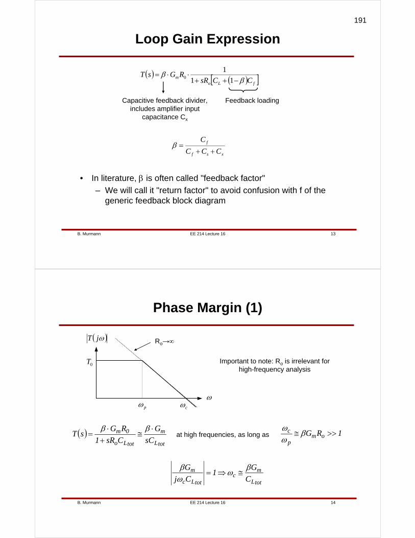
EE 214 Lecture 16B. Murmann 13
Loop Gain Expression
• In literature, β is often called "feedback factor"
– We will call it "return factor" to avoid confusion with f of thegeneric feedback block diagram
( ) ( )[ ]fLom CCsR
RGsTβ
β−++
⋅⋅=11
10
Feedback loadingCapacitive feedback divider, includes amplifier input
capacitance Cx
xsf
f
CCC
C
++=β
EE 214 Lecture 16B. Murmann 14
Phase Margin (1)
totL
mc
totLc
m
C
G1
Cj
G βωωβ
≅⇒=
pωω
( )ωjT
0T
cω
Ro→∞
( )totL
m
totLo
0m
sC
G
CsR1
RGsT
⋅≅
+⋅
=ββ
at high frequencies, as long as 1RG omp
c >>≅ βωω
Important to note: Ro is irrelevant for high-frequency analysis
191
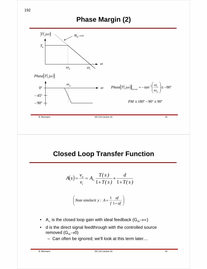
EE 214 Lecture 16B. Murmann 15
Phase Margin (2)
pωω
( )ωjT
0T
cω
( )[ ]ωjTPhase
°0
°− 45
°−90
ωpω ( )[ ] °−≅⎟
⎟⎠
⎞⎜⎜⎝
⎛−= −
=901
p
cc
tanjTPhaseωωω
ωω
°≅°−°≅ 9090180PM
Ro→∞
EE 214 Lecture 16B. Murmann 16
Closed Loop Transfer Function
( ))s(T
d
)s(T
)s(TA
v
vsA
i
o
++
+== ∞ 11
• A∞ is the closed loop gain with ideal feedback (Gm→∞)
• d is the direct signal feedthrough with the controlled source removed (Gm→0)
– Can often be ignored; we'll look at this term later…
⎟⎟⎠
⎞⎜⎜⎝
⎛+
=af
af
fA :y similaritNote
1
1
192
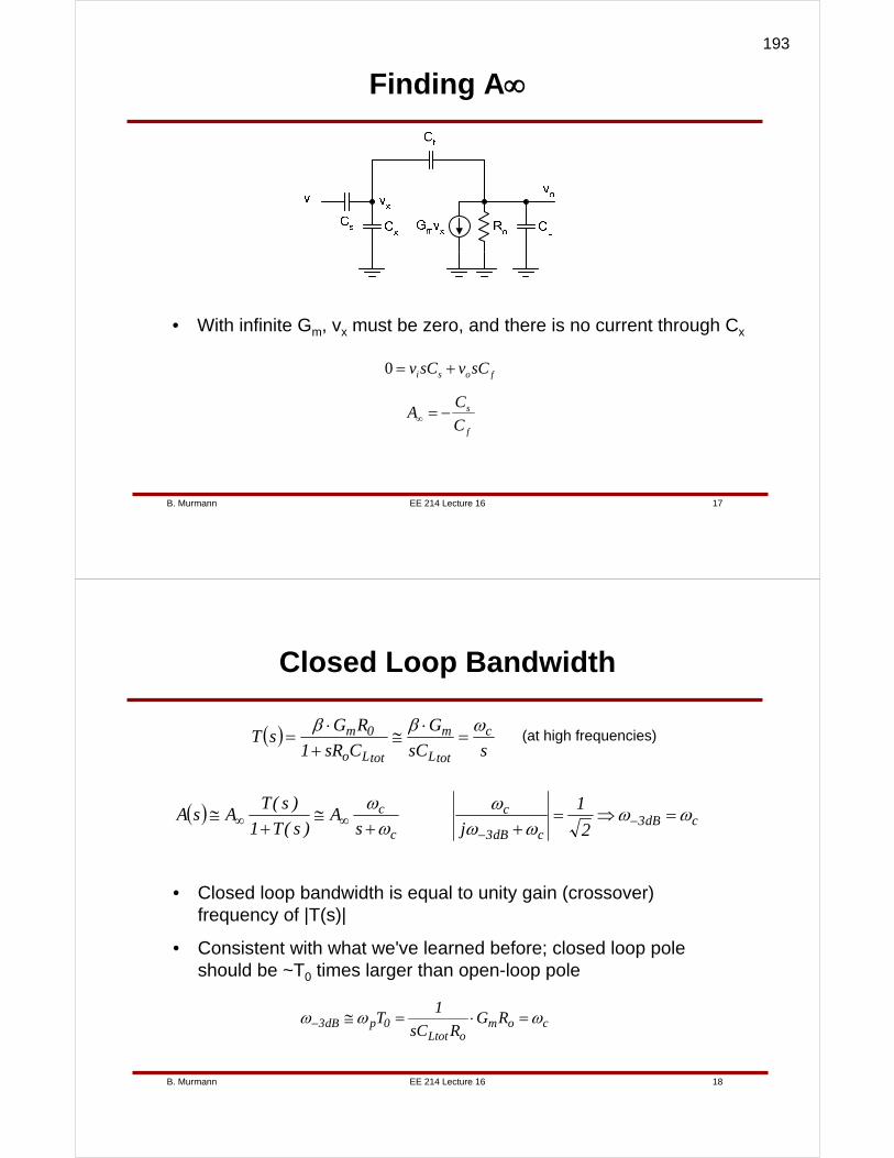
EE 214 Lecture 16B. Murmann 17
Finding A∞
• With infinite Gm, vx must be zero, and there is no current through Cx
fosi sCvsCv +=0
f
s
C
CA −=∞
EE 214 Lecture 16B. Murmann 18
Closed Loop Bandwidth
• Closed loop bandwidth is equal to unity gain (crossover) frequency of |T(s)|
• Consistent with what we've learned before; closed loop pole should be ~T0 times larger than open-loop pole
( )ssC
G
CsR1
RGsT c
totL
m
totLo
0m ωββ=
⋅≅
+⋅
= (at high frequencies)
( )c
c
sA
)s(T1
)s(TAsA
ωω+
≅+
≅ ∞∞ cdB3cdB3
c
2
1
jωω
ωωω
=⇒=+ −
−
comoLtot
0pdB3 RGRsC
1T ωωω =⋅=≅−
193
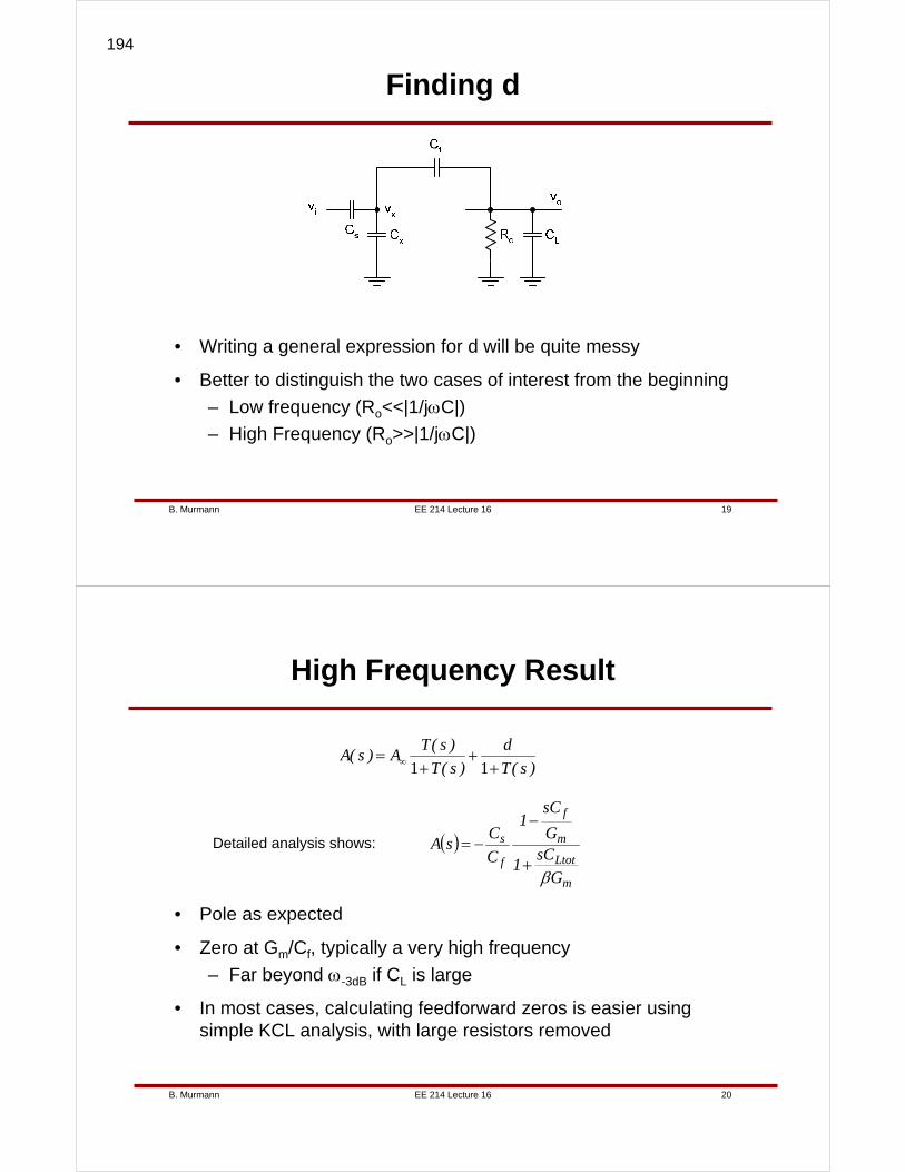
EE 214 Lecture 16B. Murmann 19
Finding d
• Writing a general expression for d will be quite messy
• Better to distinguish the two cases of interest from the beginning
– Low frequency (Ro<<|1/jωC|)
– High Frequency (Ro>>|1/jωC|)
EE 214 Lecture 16B. Murmann 20
High Frequency Result
• Pole as expected
• Zero at Gm/Cf, typically a very high frequency
– Far beyond ω-3dB if CL is large
• In most cases, calculating feedforward zeros is easier using simple KCL analysis, with large resistors removed
)s(T
d
)s(T
)s(TA)s(A
++
+= ∞ 11
( )
m
Ltot
m
f
f
s
G
sC1
G
sC1
C
CsA
β+
−−=Detailed analysis shows:
194
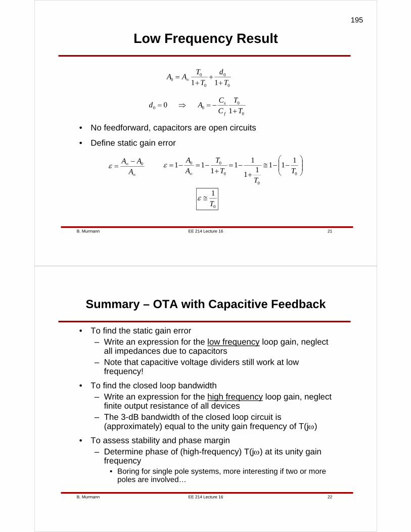
EE 214 Lecture 16B. Murmann 21
Low Frequency Result
• No feedforward, capacitors are open circuits
• Define static gain error
0
0
0
00 11 T
d
T
TAA
++
+= ∞
0
000 1
0T
T
C
CAd
f
s
+−=⇒=
∞
∞ −=A
AA 0ε ⎟⎟⎠
⎞⎜⎜⎝
⎛−−≅
+−=
+−=−=
∞ 0
0
0
00 111
11
11
111
TT
T
T
A
Aε
0
1
T≅ε
EE 214 Lecture 16B. Murmann 22
Summary – OTA with Capacitive Feedback
• To find the static gain error– Write an expression for the low frequency loop gain, neglect
all impedances due to capacitors– Note that capacitive voltage dividers still work at low
frequency!
• To find the closed loop bandwidth– Write an expression for the high frequency loop gain, neglect
finite output resistance of all devices– The 3-dB bandwidth of the closed loop circuit is
(approximately) equal to the unity gain frequency of T(jω)
• To assess stability and phase margin– Determine phase of (high-frequency) T(jω) at its unity gain
frequency• Boring for single pole systems, more interesting if two or more
poles are involved…
195

EE 214 Lecture 16B. Murmann 23
Comparison
• Two-Port Analysis
• a, f
• 1/f
• Return Ratio Analysis
• T
• A∞
T1
d
T1
TAA
++
+= ∞af1
af
f
1A
+=
(feedforward effects are not modeled)
196
EE 214 Lecture 17B. Murmann 1
Lecture 17Loop Gain Simulation
Boris MurmannStanford University
Copyright © 2007 by Boris Murmann
EE 214 Lecture 17B. Murmann 2
Overview
• Introduction
– Last lecture, we've seen that return ratio analysis is a useful tool for characterizing feedback amplifiers in terms of stability, bandwidth and static precision. Since we are always interested in verifying our hand analysis results using simulations, it is desirable to have an equivalent method available in Spice. In this lecture, we will discuss the so-called Middlebrook method for loop gain simulation. This particular approach helps overcome the issue that ideal loop breakpoints, e.g. at controlled sources, are not directly accessible in Spice.
197
EE 214 Lecture 17B. Murmann 3
References
• H.W. Bode, Network Analysis and Feedback Amplifier Design, Van Nostrand, New York, 1945.
• R.D. Middlebrook, "Measurement of Loop Gain in Feedback Systems," Int. J. Electronics, Vol. 38, No.4, .pp. 485-512, 1975.
• S. Rosenstark, "Loop Gain Measurement in Feedback Amplifiers," Int. J. Electronics, Vol. 57, No.3., pp. 415-421, 1984.
• P.J. Hurst, "Exact Simulation of Feedback Circuit Parameters," Trans. on Circuits and Systems, pp.1382-1389, Nov. 1991.
• P.J. Hurst, S.H. Lewis, "Simulation of Return Ratio in Fully Differential Feedback Circuits," Proc. CICC 1994, pp.29-32.
• Ken Kundert, "A Test Bench for Differential Circuits," Online: http://www.designers-guide.com/Analysis/diff.pdf
• M. Tian, V. Visvanathan, J. Hantgan, K. Kundert, "Striving for small-signal stability," IEEE Circuits and Devices Magazine, pp. 31-41, January 2001.
EE 214 Lecture 17B. Murmann 4
Circuit Example 1
• What is the loop gain in this circuit?
198
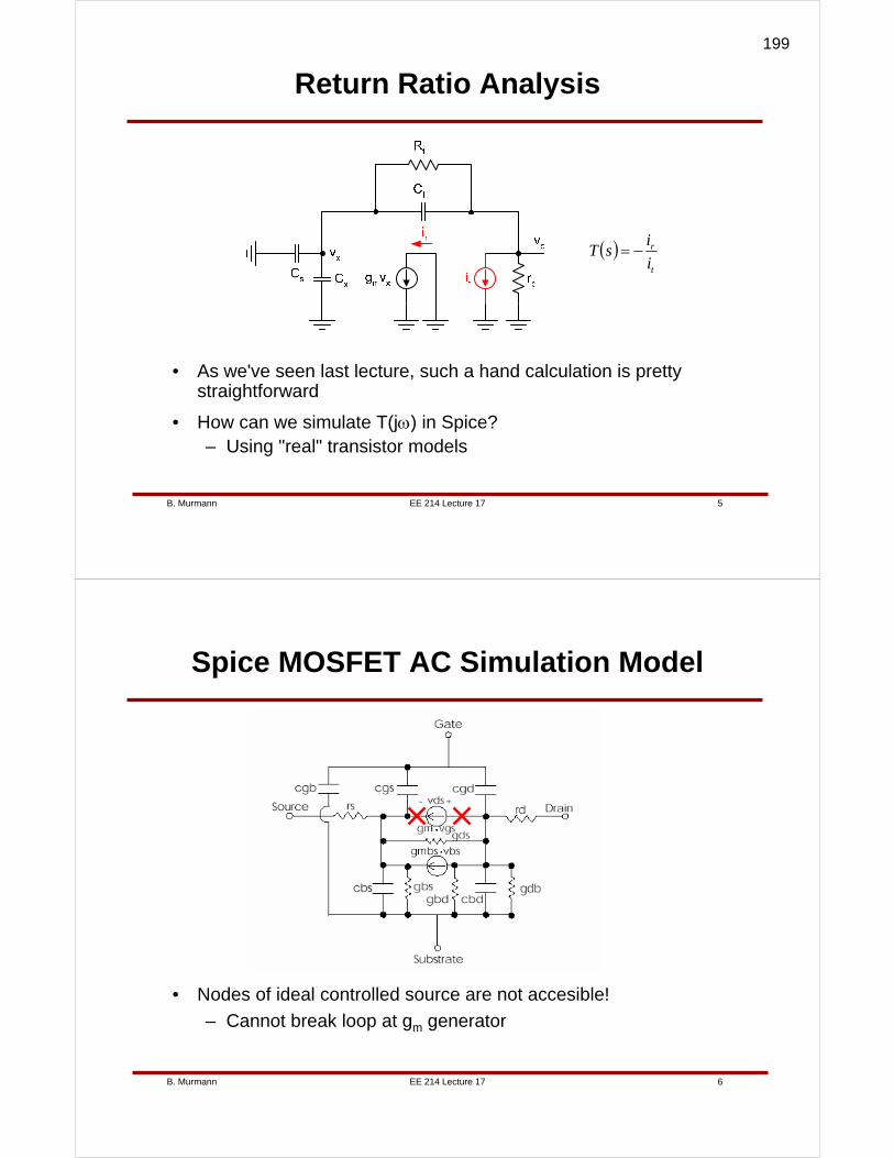
EE 214 Lecture 17B. Murmann 5
Return Ratio Analysis
• As we've seen last lecture, such a hand calculation is pretty straightforward
• How can we simulate T(jω) in Spice?– Using "real" transistor models
( )t
r
i
isT −=
EE 214 Lecture 17B. Murmann 6
Spice MOSFET AC Simulation Model
• Nodes of ideal controlled source are not accesible!
– Cannot break loop at gm generator
199
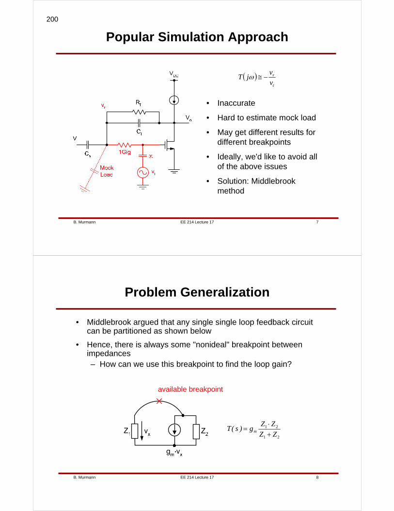
EE 214 Lecture 17B. Murmann 7
Popular Simulation Approach
• Inaccurate
• Hard to estimate mock load
• May get different results for different breakpoints
• Ideally, we'd like to avoid all of the above issues
• Solution: Middlebrook method
( )t
r
v
vjT −≅ω
EE 214 Lecture 17B. Murmann 8
Problem Generalization
• Middlebrook argued that any single single loop feedback circuit can be partitioned as shown below
• Hence, there is always some "nonideal" breakpoint between impedances– How can we use this breakpoint to find the loop gain?
available breakpoint
21
21
ZZ
ZZg)s(T m +
⋅=
200
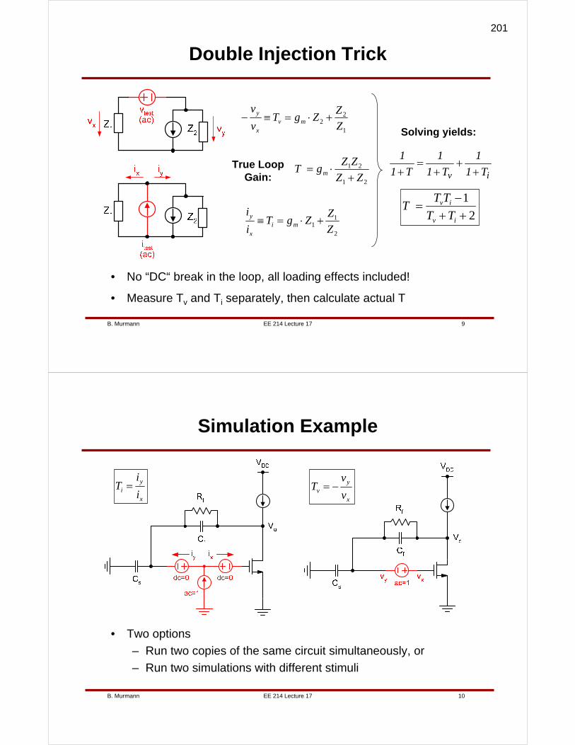
EE 214 Lecture 17B. Murmann 9
Double Injection Trick
• No “DC“ break in the loop, all loading effects included!
• Measure Tv and Ti separately, then calculate actual T
1
22 Z
ZZgT
v
vmv
x
y +⋅=≡−
2
11 Z
ZZgT
i
imi
x
y +⋅=≡
21
21
ZZ
ZZgT m +
⋅=True Loop Gain:
Solving yields:
2
1
++−
=iv
iv
TT
TTT
iv T1
1
T1
1
T1
1
++
+=
+
EE 214 Lecture 17B. Murmann 10
Simulation Example
• Two options
– Run two copies of the same circuit simultaneously, or
– Run two simulations with different stimuli
x
yv v
vT −=
x
yi i
iT =
201
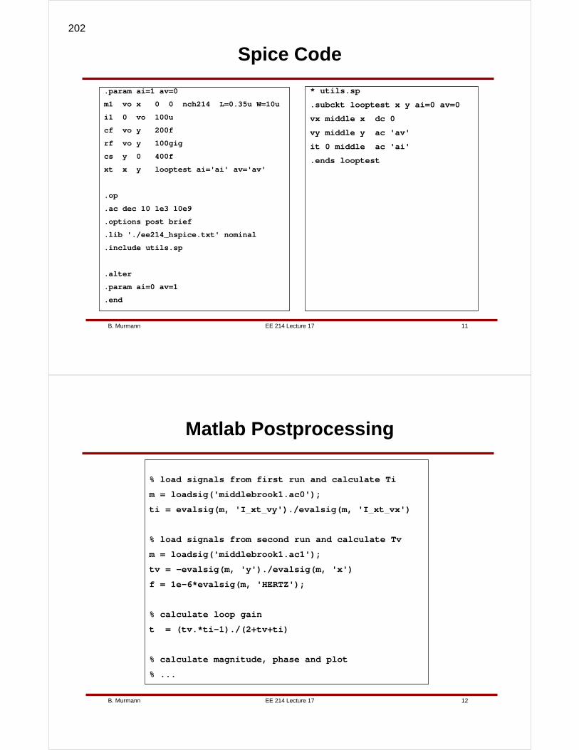
EE 214 Lecture 17B. Murmann 11
Spice Code
.param ai=1 av=0
m1 vo x 0 0 nch214 L=0.35u W=10u
i1 0 vo 100u
cf vo y 200f
rf vo y 100gig
cs y 0 400f
xt x y looptest ai='ai' av='av'
.op
.ac dec 10 1e3 10e9
.options post brief
.lib './ee214_hspice.txt' nominal
.include utils.sp
.alter
.param ai=0 av=1
.end
* utils.sp
.subckt looptest x y ai=0 av=0
vx middle x dc 0
vy middle y ac 'av'
it 0 middle ac 'ai'
.ends looptest
EE 214 Lecture 17B. Murmann 12
Matlab Postprocessing
% load signals from first run and calculate Ti
m = loadsig('middlebrook1.ac0');
ti = evalsig(m, 'I_xt_vy')./evalsig(m, 'I_xt_vx')
% load signals from second run and calculate Tv
m = loadsig('middlebrook1.ac1');
tv = -evalsig(m, 'y')./evalsig(m, 'x')
f = 1e-6*evalsig(m, 'HERTZ');
% calculate loop gain
t = (tv.*ti-1)./(2+tv+ti)
% calculate magnitude, phase and plot
% ...
202
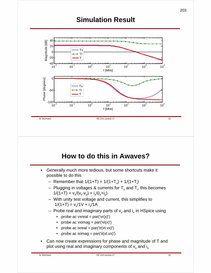
EE 214 Lecture 17B. Murmann 13
Simulation Result
10-2
10-1
100
101
102
103
104
-40
-20
0
20
40
f [MHz]
Ma
gn
itud
e [d
B]
TvTiT
10-2
10-1
100
101
102
103
104
-100
-50
0
f [MHz]
Ph
ase
[de
gre
es]
TvTiT
EE 214 Lecture 17B. Murmann 14
How to do this in Awaves?
• Generally much more tedious, but some shortcuts make it possible to do this
– Remember that 1/(1+T) = 1/(1+Tv) + 1/(1+Ti)
– Plugging in voltages & currents for Tv and Ti, this becomes 1/(1+T) = vx/(vx-vy) + ix/(ix+iy)
– With unity test voltage and current, this simplifies to1/(1+T) = vx/1V + ix/1A
– Probe real and imaginary parts of vx and ix in HSpice using• .probe ac vxreal = par('vr(x)')
• .probe ac vximag = par('vi(x)')
• .probe ac ixreal = par('ir(xt.vx)')
• .probe ac iximag = par('ii(xt.vx)')
• Can now create expressions for phase and magnitude of T and plot using real and imaginary components of vx and ix
203
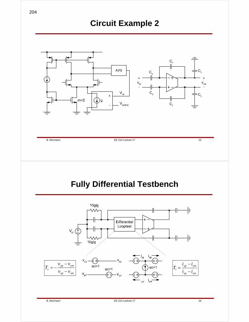
EE 214 Lecture 17B. Murmann 15
Circuit Example 2
Cs
+vid-
+vod-
Cs
Cf
Cf
CL
CL
EE 214 Lecture 17B. Murmann 16
Fully Differential Testbench
xmxp
ymypv vv
vvT
−
−−=
xmxp
ymypi ii
iiT
−
−=
204
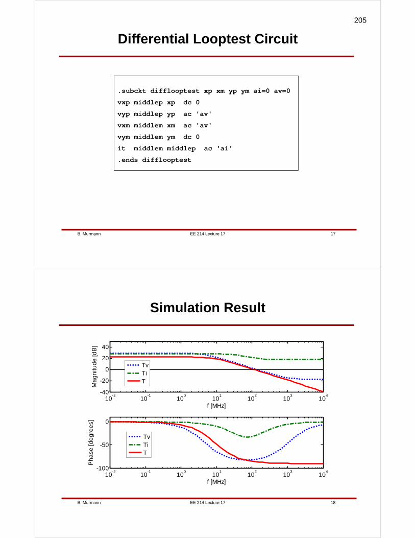
EE 214 Lecture 17B. Murmann 17
Differential Looptest Circuit
.subckt difflooptest xp xm yp ym ai=0 av=0
vxp middlep xp dc 0
vyp middlep yp ac 'av'
vxm middlem xm ac 'av'
vym middlem ym dc 0
it middlem middlep ac 'ai'
.ends difflooptest
EE 214 Lecture 17B. Murmann 18
Simulation Result
10-2
10-1
100
101
102
103
104
-40
-20
0
20
40
f [MHz]
Ma
gn
itud
e [d
B]
10-2
10-1
100
101
102
103
104
-100
-50
0
f [MHz]
Ph
ase
[de
gre
es]
TvTiT
TvTiT
205
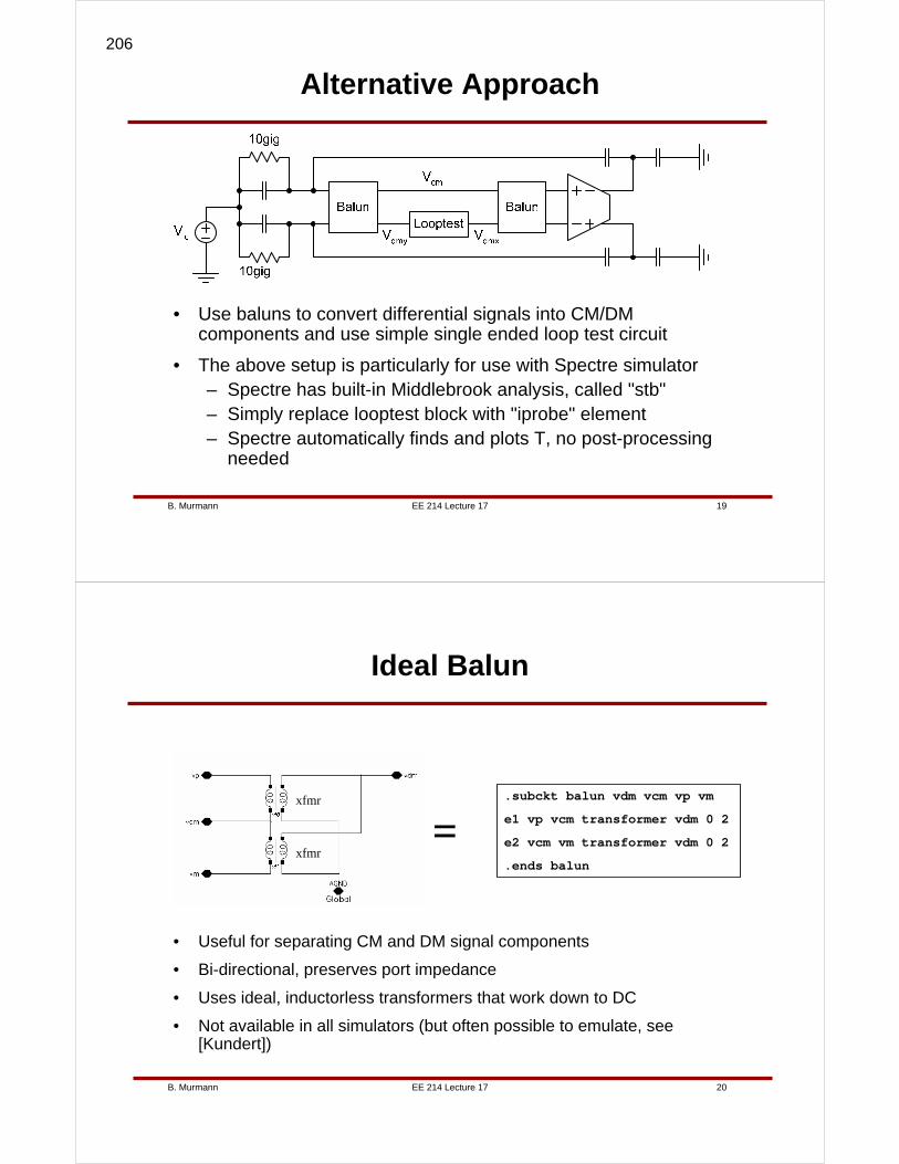
EE 214 Lecture 17B. Murmann 19
Alternative Approach
• Use baluns to convert differential signals into CM/DM components and use simple single ended loop test circuit
• The above setup is particularly for use with Spectre simulator– Spectre has built-in Middlebrook analysis, called "stb"– Simply replace looptest block with "iprobe" element– Spectre automatically finds and plots T, no post-processing
needed
EE 214 Lecture 17B. Murmann 20
xfmr
xfmr
Ideal Balun
• Useful for separating CM and DM signal components
• Bi-directional, preserves port impedance
• Uses ideal, inductorless transformers that work down to DC
• Not available in all simulators (but often possible to emulate, see [Kundert])
=.subckt balun vdm vcm vp vm
e1 vp vcm transformer vdm 0 2
e2 vcm vm transformer vdm 0 2
.ends balun
206

EE 214 Lecture 17B. Murmann 21
+ New Middlebrook Method
• Recently, Middlebrook came up with an alternative way of looking at feedback circuits
– A more "design oriented analysis"
• He titled this approach "The General Feedback Theorem – A final solution for feedback systems"
• If you are curious about this new method, please refer to
– http://rdmiddlebrook.com
– http://ardem.com/free_downloads.asp
– http://groups.yahoo.com/group/Design-Oriented_Analysis_D-OA/
EE 214 Lecture 17B. Murmann 22
Multi Loop Considerations
• Any practical feedback circuit has multiple feedback loops
– Fully differential circuits have CM/DM loops
– Local device feedback through Cgd, Rsource
– ...
• Solutions
– Decompose fully differential circuit into CM/DM loops
– If a local feedback loop can be modeled as a combination of a stable controlled source and passive impedances, the multi-loop circuit reduces to a single loop [Hurst 94]
– If there is a common breakpoint that breaks all feedback loops simultaneosly, stability can be checked by finding the return ratio at the single breakpoint [Hurst 94]
207

EE 214 Lecture 17B. Murmann 23
Last Resort: General Nyquist Criterion
[Bode 45]:
“If a circuit is stable when all its tubes have their nominal gains, the total number of clockwise and counterclockwise encirclements of the critical point must be equal to each other in the series of Nyquist diagrams for the individual tubes obtained by beginning with all tubes dead and restoring the tubes successively in any order to their nominal gains“
[You may want to take a controls class if you are interested in this...]
EE 214 Lecture 17B. Murmann 24
[Bode 45]:
“... thus the circuit may sing when the tubes begin to lose their gain because of age, and it may also sing, instead of behaving as it should, when the gain increases from zero as power is supplied to the circuit...“
Another Useful Quote
Always run one or more transient analyses for a "true" stability check!
208

EE 214 Lecture 18B. Murmann 1
Lecture 18Differential Mode Voltage Range
Two-Stage OTA
Boris MurmannStanford University
Copyright © 2007 by Boris Murmann
EE 214 Lecture 18B. Murmann 2
Overview
• Reading
– 6.3 (Basic Two-Stage MOS Amplifiers)
– 12.6.1 (Fully Differential Two-Stage-Amplifier)
– 12.6.5 (Neutralization)
• Introduction
– As we will see in today's lecture, the available output swing and open-loop gain of our simple single stage OTA are fairly limited. Hence, we will begin to consider a two-stage OTA architecture as an alternative. Unfortunately, with the addition of a second stage, we also introduce a second pole, which makes it difficult to achieve reasonable phase margin. The compensation techniques discussed in the following lecture will provide solutions to this problem.
209

EE 214 Lecture 18B. Murmann 3
Output Swing of Simple OTA
• Available output swing depends on input and output common mode levels
• May be limited by headroom for differential pair device (Vminn) or active load (Vminp)
EE 214 Lecture 18B. Murmann 4
Maximum Available Swing
• Input and output common mode adjusted such that all devices operate at "edge" of forward active region
– Well defined using long channel model, very gradual transition in short channels
• Unfortunately, the choice of Vic and Voc are often dictated by the circuits that interface with the amplifier
– E.g. Vic=Voc=1.5V( )tminnminpminDDmax,odpp VVVVV −−−= 2
210
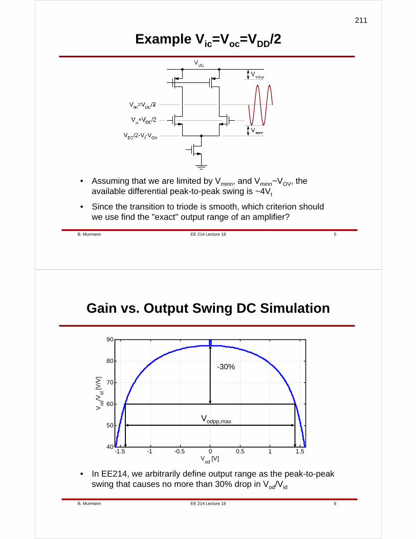
EE 214 Lecture 18B. Murmann 5
Example Vic=Voc=VDD/2
• Assuming that we are limited by Vminn, and Vminn~VOV, the available differential peak-to-peak swing is ~4Vt
• Since the transition to triode is smooth, which criterion shouldwe use find the "exact" output range of an amplifier?
EE 214 Lecture 18B. Murmann 6
Gain vs. Output Swing DC Simulation
• In EE214, we arbitrarily define output range as the peak-to-peak swing that causes no more than 30% drop in Vod/Vid
-1.5 -1 -0.5 0 0.5 1 1.540
50
60
70
80
90
Vod
[V]
Vod
/Vid
[V/V
]
-30%
Vodpp,max
211
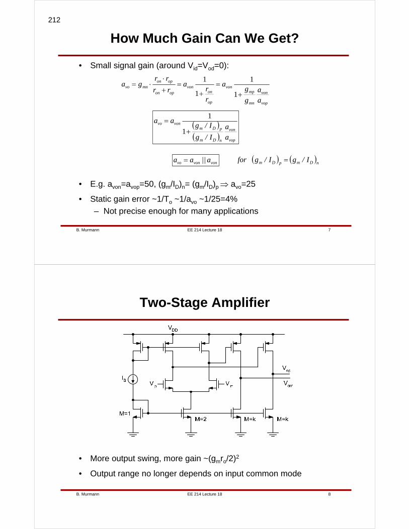
EE 214 Lecture 18B. Murmann 7
How Much Gain Can We Get?
• Small signal gain (around Vid=Vod=0):
vop
von
mn
mpvon
op
onvon
opon
oponmnvo
aa
g
ga
rr
arr
rrga
+=
+=
+
⋅⋅=
1
1
1
1
( )( ) vop
von
nDm
pDmvonvo
aa
I/g
I/gaa
+=
1
1
vonvonvo a||aa = ( ) ( )nDmpDm I/gI/g for =
• E.g. avon=avop=50, (gm/ID)n= (gm/ID)p ⇒ avo=25
• Static gain error ~1/To ~1/avo ~1/25=4%
– Not precise enough for many applications
EE 214 Lecture 18B. Murmann 8
Two-Stage Amplifier
• More output swing, more gain ~(gmro/2)2
• Output range no longer depends on input common mode
212
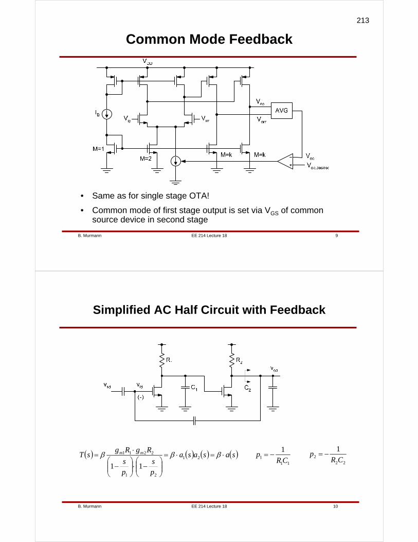
EE 214 Lecture 18B. Murmann 9
Common Mode Feedback
• Same as for single stage OTA!
• Common mode of first stage output is set via VGS of common source device in second stage
EE 214 Lecture 18B. Murmann 10
Simplified AC Half Circuit with Feedback
( ) ( ) ( ) ( )sasasa
ps
ps
RgRgsT mm ⋅=⋅=
⎟⎟⎠
⎞⎜⎜⎝
⎛−⋅⎟⎟
⎠
⎞⎜⎜⎝
⎛−
⋅= βββ 21
21
2211
11 111
1
CRp −=
222
1
CRp −=
213
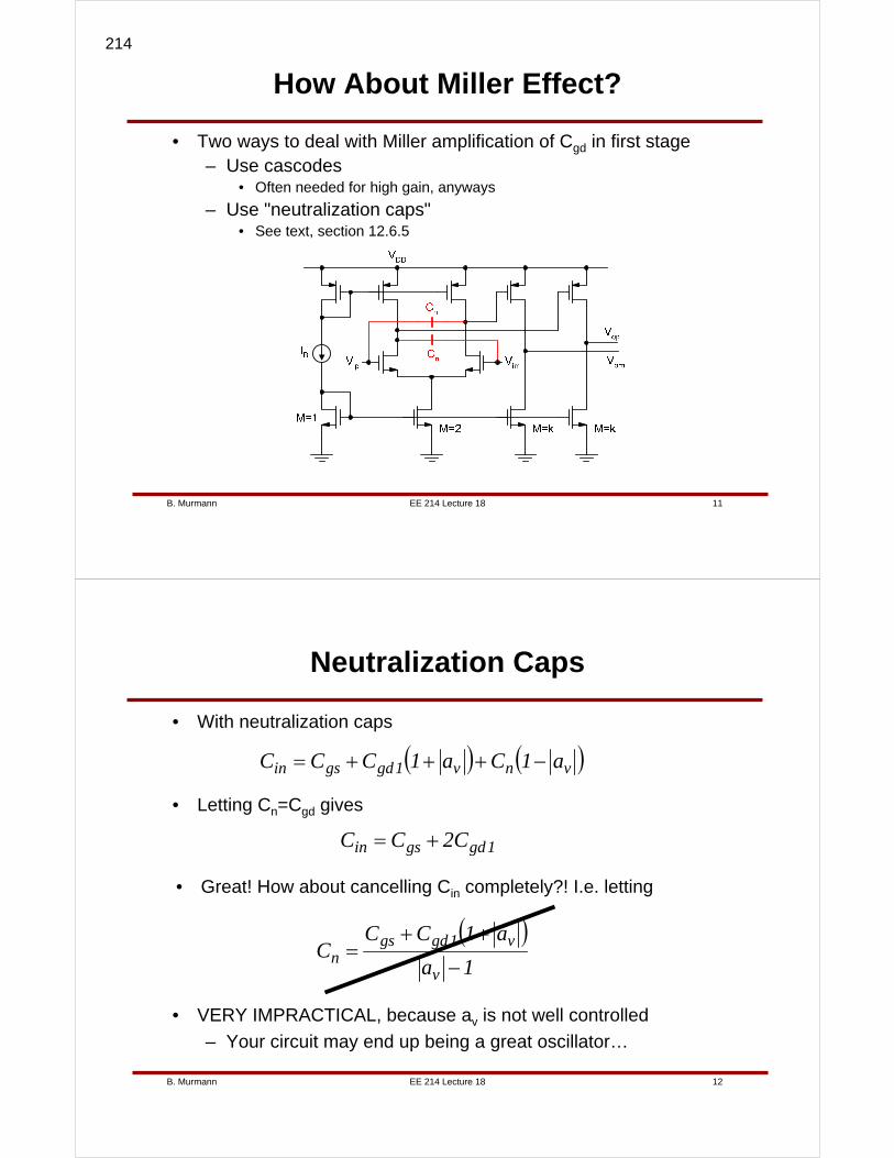
EE 214 Lecture 18B. Murmann 11
How About Miller Effect?
• Two ways to deal with Miller amplification of Cgd in first stage– Use cascodes
• Often needed for high gain, anyways
– Use "neutralization caps"• See text, section 12.6.5
EE 214 Lecture 18B. Murmann 12
Neutralization Caps
• With neutralization caps
( ) ( )vnv1gdgsin a1Ca1CCC −+++=
• Letting Cn=Cgd gives
1gdgsin C2CC +=
• Great! How about cancelling Cin completely?! I.e. letting
( )1a
a1CCC
v
v1gdgsn −
++=
• VERY IMPRACTICAL, because av is not well controlled
– Your circuit may end up being a great oscillator…
214
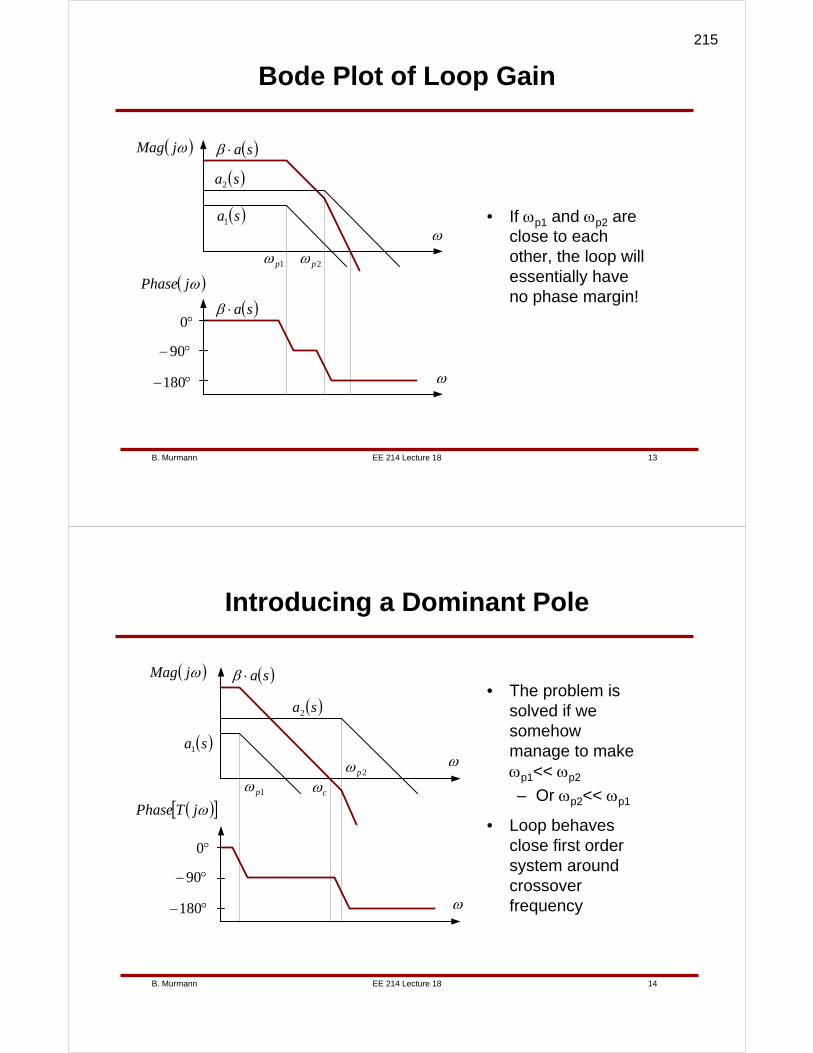
EE 214 Lecture 18B. Murmann 13
Bode Plot of Loop Gain
• If ωp1 and ωp2 are close to each other, the loop will essentially have no phase margin!
ω
1pω
°0
°−90
°−180 ω
2pω
( )ωjMag
( )ωjPhase
( )sa1
( )sa⋅β
( )sa2
( )sa⋅β
EE 214 Lecture 18B. Murmann 14
Introducing a Dominant Pole
• The problem is solved if we somehow manage to make ωp1<< ωp2
– Or ωp2<< ωp1
• Loop behaves close first order system around crossover frequency
ω
1pω
°0
°−90
°−180 ω
2pω
( )ωjMag
( )[ ]ωjTPhase
( )sa1
( )sa⋅β
( )sa2
cω
215

EE 214 Lecture 18B. Murmann 15
Phase Margin
• At the crossover frequency, the dominant pole has shifted the phase by about -90°
• The non-dominant pole's phase at ωc is given by -tan-1(ωc/ωp2)
⎟⎟⎠
⎞⎜⎜⎝
⎛−°−°≅ −
2
190180p
ctanPMωω
⎟⎟⎠
⎞⎜⎜⎝
⎛≅ −
c
ptanPMωω 21
72°3
76°4
79°5
63°2
45°1
PMωp2/ωc
EE 214 Lecture 18B. Murmann 16
Creating a Dominant Pole
• Numerical example:
mSGG mm 121 == Ω== kRR 10021 pFC 12 =
MHz.CR
f p 612
1
222 ==
π
°= 72PM
kHzf
f pc 530
32 == Hz
RGRG
ff
mm
cp 106
22111 =
⋅⋅=β
50.=β
nFRf
Cp
152
1
111 =
⋅⋅=
π
• Two issues
– Very low fc, which means low closed loop bandwidth
– Huge capacitor• Get roughly 1fF/μm2 in CMOS technology
• C1 would occupy about 4mm x 4mm !
216
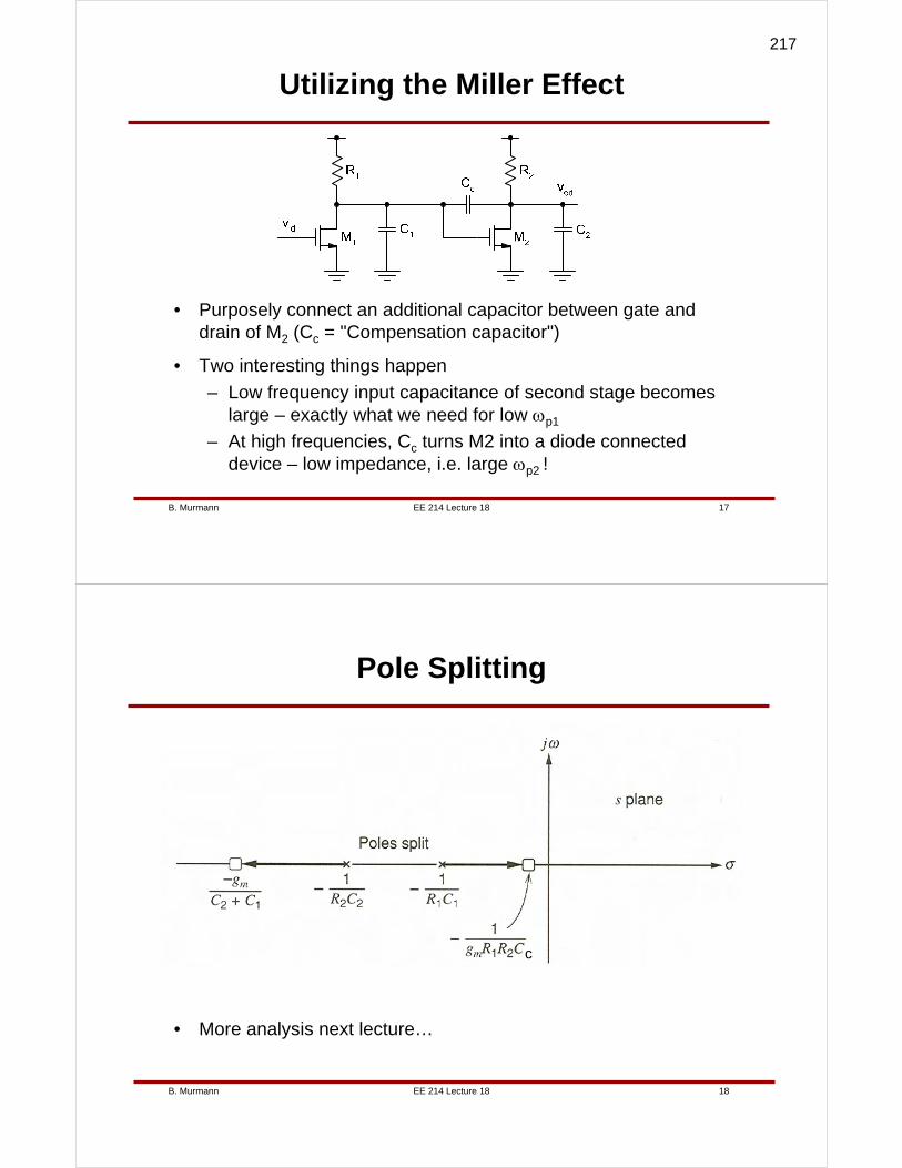
EE 214 Lecture 18B. Murmann 17
Utilizing the Miller Effect
• Purposely connect an additional capacitor between gate and drain of M2 (Cc = "Compensation capacitor")
• Two interesting things happen
– Low frequency input capacitance of second stage becomes large – exactly what we need for low ωp1
– At high frequencies, Cc turns M2 into a diode connected device – low impedance, i.e. large ωp2 !
EE 214 Lecture 18B. Murmann 18
Pole Splitting
• More analysis next lecture…
c
217

EE 214 Lecture 19B. Murmann 1
Lecture 19Compensation
Noise in Feedback OTAs
Boris MurmannStanford University
Copyright © 2007 by Boris Murmann
EE 214 Lecture 19B. Murmann 2
Overview
• Reading
– 9.4.1, 9.4.2, 9.4.3 (Compensation)
• Introduction
– In this lecture, we will continue to look at pole splitting as amethod for achieving sufficient phase margin in a two-stage amplifier. While using a Miller capacitance for compensation helps move the non-dominant pole to higher frequency, it also introduces an undesired zero in the transfer function. Today, we'll discuss several options on how to cope with this artifact.
– In addition, we will derive useful expressions for the total integrated noise in OTAs.
218

EE 214 Lecture 19B. Murmann 3
Two-Stage OTA with Cc
• Detailed analysis shows:
( ) ( ) ( )[ ] ( )1c2c21212
c122m1c12c2
2m
c22m11m
i
o
CCCCCCRRsCRRgRCCRCCs1
g
Cs1RgRg
v
vsa
++++++++
⎟⎟⎠
⎞⎜⎜⎝
⎛−⋅⋅
==
• Very messy…
EE 214 Lecture 19B. Murmann 4
Dominant Pole Approximation
• We can write the denominator as
( )21
2
2121
11111
pp
s
pps
p
s
p
ssD +⎟⎟
⎠
⎞⎜⎜⎝
⎛+−=⎟⎟
⎠
⎞⎜⎜⎝
⎛−⋅⎟⎟
⎠
⎞⎜⎜⎝
⎛−=
• Since in a practical design outcome we'll have |p1|<<|p2|, we can approximate
( )21
2
1
11
pp
s
pssD +⎟⎟
⎠
⎞⎜⎜⎝
⎛−≅
• With this simplification, we can now easily identify p1 and p2 by comparing the coefficients with the expression from the previousslide
219
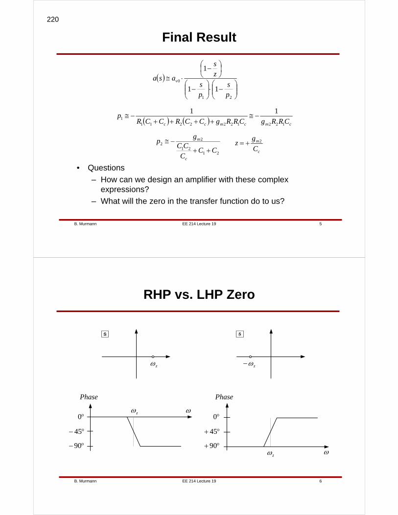
EE 214 Lecture 19B. Murmann 5
Final Result
• Questions
– How can we design an amplifier with these complex expressions?
– What will the zero in the transfer function do to us?
( )⎟⎟⎠
⎞⎜⎜⎝
⎛−⋅⎟⎟
⎠
⎞⎜⎜⎝
⎛−
⎟⎠⎞
⎜⎝⎛ −
⋅≅
21
0
11
1
ps
ps
zs
asa v
c
m
C
gz 2+=
( ) ( ) cmcmcc CRRgCRRgCCRCCRp
12212222111
11−≅
++++−≅
2121
22
CCCCC
gp
c
m
++−≅
EE 214 Lecture 19B. Murmann 6
RHP vs. LHP Zero
Phase
°0
°− 45
°−90
ωzω
zω zω−
Phase
°0
°+ 45
°+ 90ω
zω
220
EE 214 Lecture 19B. Murmann 7
OTA Transfer Function with RHP Zero
• RHP zero will reduce phase margin
– Unless gm2 >> βgm1
c
mc C
g 1βω ≅
c
mz C
g 2=ω
1
21
m
m
c
z
g
g
βωω
=
ωz
(assuming zero is beyond crossover)
EE 214 Lecture 19B. Murmann 8
Mitigating the Impact of RHP Zero
• Create unilateral feedback through Cc
– Source follower
– Cascode compensation• Ahuja, IEEE J. Solid-State Ckts., 12/1983
• Ribner, IEEE J. Solid-State Ckts., 12/1984
• "Nulling resistor"
– Push zero to infinity
– Push zero into LHP and cancel nondominant pole (!)
221
EE 214 Lecture 19B. Murmann 9
Source Follower
• Mitigates feedforward path issue
• Problems: Reduced output swing, additional power dissipation
EE 214 Lecture 19B. Murmann 10
Cascode Compensation (1)
• Cc sees low impedance, output of first stage sees high impedance looking into cascode device
– Reduced feedforward
222
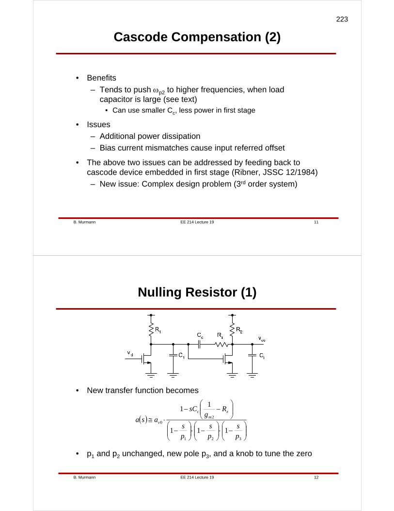
EE 214 Lecture 19B. Murmann 11
Cascode Compensation (2)
• Benefits
– Tends to push ωp2 to higher frequencies, when load capacitor is large (see text)
• Can use smaller Cc, less power in first stage
• Issues
– Additional power dissipation
– Bias current mismatches cause input referred offset
• The above two issues can be addressed by feeding back to cascode device embedded in first stage (Ribner, JSSC 12/1984)
– New issue: Complex design problem (3rd order system)
EE 214 Lecture 19B. Murmann 12
Nulling Resistor (1)
• New transfer function becomes
( )⎟⎟⎠
⎞⎜⎜⎝
⎛−⋅⎟⎟
⎠
⎞⎜⎜⎝
⎛−⋅⎟⎟
⎠
⎞⎜⎜⎝
⎛−
⎟⎟⎠
⎞⎜⎜⎝
⎛−−
⋅≅
321
20
111
11
ps
ps
ps
Rg
sC
asaz
mc
v
• p1 and p2 unchanged, new pole p3, and a knob to tune the zero
223

EE 214 Lecture 19B. Murmann 13
Nulling Resistor (2)
• Rz=1/gm2 pushes the zero to +∞– Can use a transistor in triode region to implement resistor
• Helps track process variations
EE 214 Lecture 19B. Murmann 14
Nulling Resistor (3)
• Rz=(1+C2/Cc)/gm places zero on top of ωp2!– Cancels p2
– Good in theory, may be troublesome in practice– If the pole and zero don't fall exactly on top of each other, we
get a so-called pole-zero doublet• Can cause very slow settling tails in transient response
– B.Y.T Kamath, R.G. Meyer and P.R. Gray, "Relationship between frequency response and settling time of operational amplifiers," IEEE JSSC, Vol. 9, No. 6, pp.347–352, Dec. 1974.
• See supplementary handout "Effect of Doublet on Amplifier Settling Time" (optional)
• Third pole
1
2
13
1
C
g
CRm
zp ≅≅ω 1
1
11
23 >>= typically C
C
g
g c
m
m
c
p
βωω
224
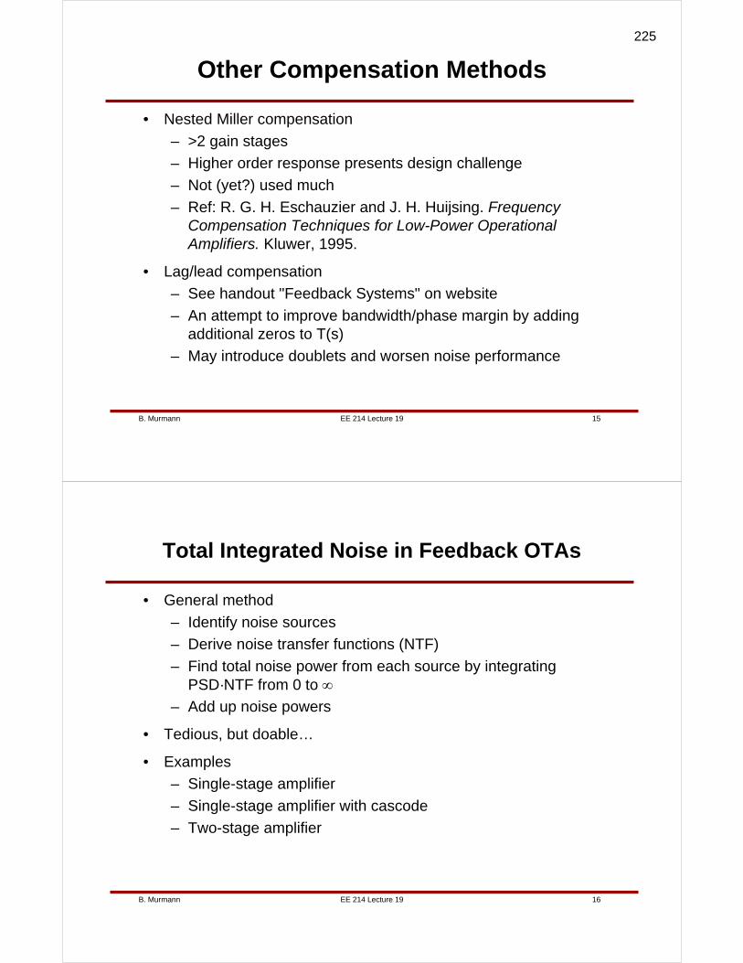
EE 214 Lecture 19B. Murmann 15
Other Compensation Methods
• Nested Miller compensation
– >2 gain stages
– Higher order response presents design challenge
– Not (yet?) used much
– Ref: R. G. H. Eschauzier and J. H. Huijsing. Frequency Compensation Techniques for Low-Power Operational Amplifiers. Kluwer, 1995.
• Lag/lead compensation
– See handout "Feedback Systems" on website
– An attempt to improve bandwidth/phase margin by adding additional zeros to T(s)
– May introduce doublets and worsen noise performance
EE 214 Lecture 19B. Murmann 16
Total Integrated Noise in Feedback OTAs
• General method
– Identify noise sources
– Derive noise transfer functions (NTF)
– Find total noise power from each source by integrating PSD·NTF from 0 to ∞
– Add up noise powers
• Tedious, but doable…
• Examples
– Single-stage amplifier
– Single-stage amplifier with cascode
– Two-stage amplifier
225
EE 214 Lecture 19B. Murmann 17
Useful Integrals
EE 214 Lecture 19B. Murmann 18
Single Stage Amplifier
CL+vi-
+vo-
M1
M2VB
Cf
Cs
⎟⎟⎠
⎞⎜⎜⎝
⎛+⎟
⎟⎠
⎞⎜⎜⎝
⎛++=
⎟⎟⎠
⎞⎜⎜⎝
⎛+=
∞1m
2m
f
1gg
Ltot
1m
2m
Ltot
2tot,o
g
g1
C
CA1
C
kT
g
g1
C
kTv
γ
βγ
• Make gm2 as small as possible, i.e. use small gm/ID for current source device
– Issue: Smaller gm/ID means less available swing
• Small Cgg1, i.e. high fT helps reduce noise
( )β−++= 1CCCC fjunctionLLtot
226
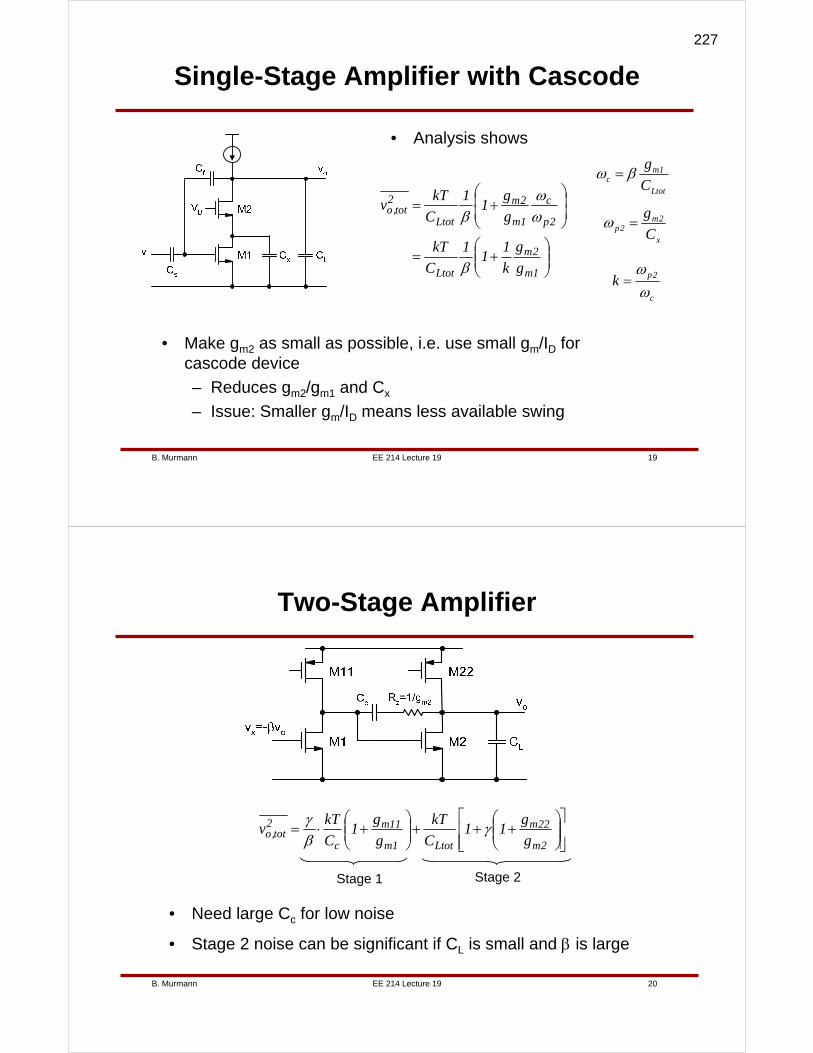
EE 214 Lecture 19B. Murmann 19
Single-Stage Amplifier with Cascode
• Analysis shows
⎟⎟⎠
⎞⎜⎜⎝
⎛+=
⎟⎟⎠
⎞⎜⎜⎝
⎛+=
1m
2m
Ltot
2p
c
1m
2m
Ltot
2tot,o
g
g
k
11
1
C
kT
g
g1
1
C
kTv
β
ωω
β
• Make gm2 as small as possible, i.e. use small gm/ID for cascode device
– Reduces gm2/gm1 and Cx
– Issue: Smaller gm/ID means less available swing
Ltot
1mc C
gβω =
x
2m2p C
g=ω
c
2pkωω
=
EE 214 Lecture 19B. Murmann 20
Two-Stage Amplifier
• Need large Cc for low noise
• Stage 2 noise can be significant if CL is small and β is large
⎥⎥⎦
⎤
⎢⎢⎣
⎡⎟⎟⎠
⎞⎜⎜⎝
⎛+++⎟⎟
⎠
⎞⎜⎜⎝
⎛+⋅=
2m
22m
Ltot1m
11m
c
2tot,o g
g11
C
kT
g
g1
C
kTv γ
βγ
Stage 1 Stage 2
227
EE 214 Lecture 19B. Murmann 21
SNR in Differential Circuits
• In fully differential circuits, the effective output swing is doubled
– But there are two half circuits that contribute noise
• Signal power increases by 4x, noise power increases by 2x
– 3dB win in terms of SNR
– At the cost of twice the power consumption (no free lunch…)
CkTV
SNR2
o∝
EE 214 Lecture 19B. Murmann 22
Appendix
"Noise in a Two-stage OTA with Nulling Resistor"
228
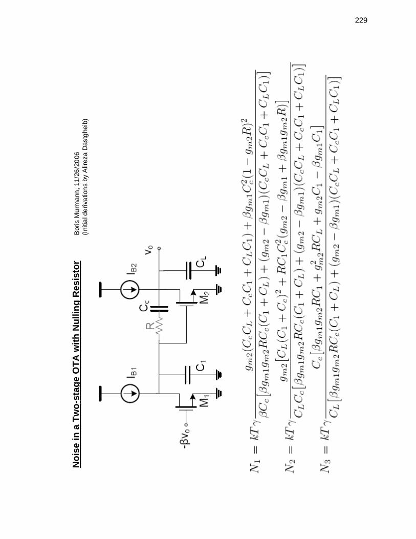
Noi
se in
a T
wo-
stag
e O
TA w
ith N
ullin
g R
esis
tor
Bor
is M
urm
ann,
11/
26/2
006
(Initi
al d
eriv
atio
ns b
y A
lirez
a D
astg
heib
)
229
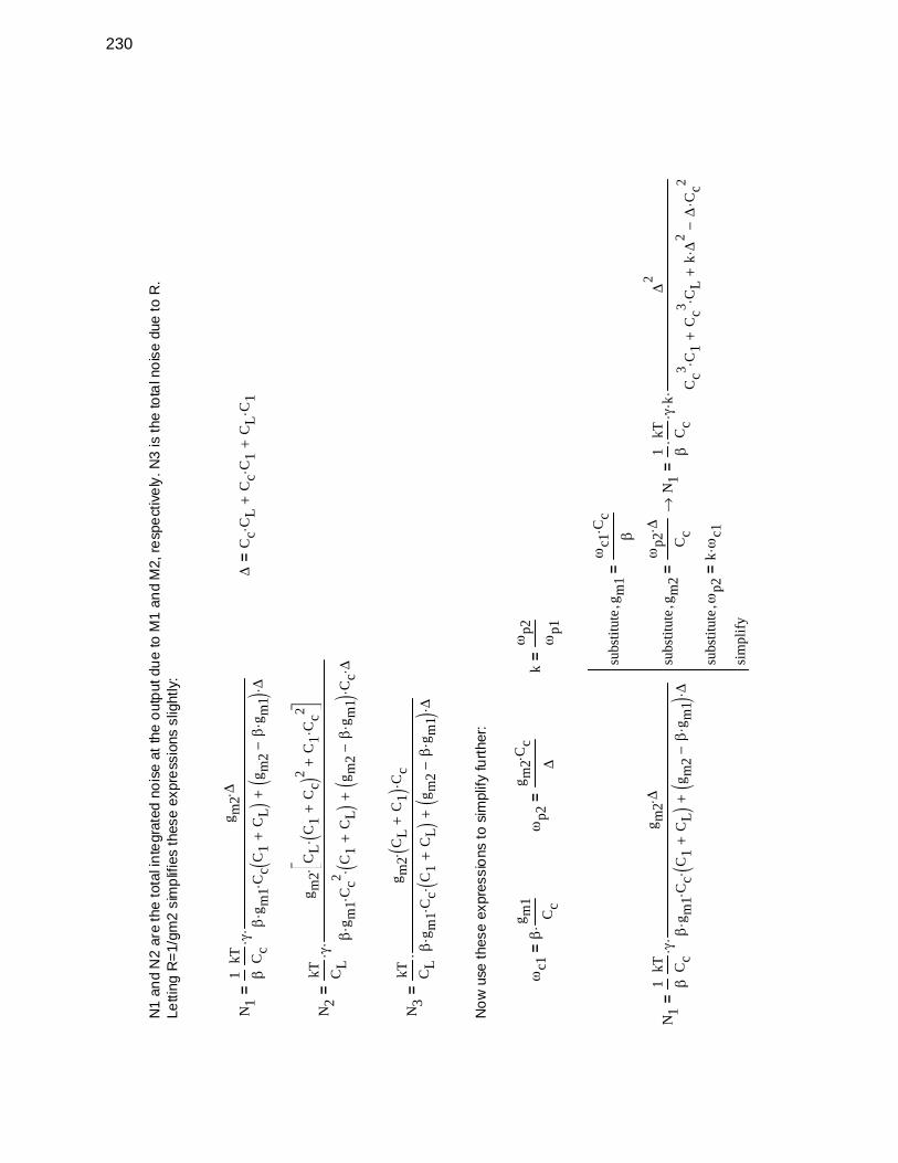
N1
and
N2
are
the
tota
l int
egra
ted
nois
e at
the
outp
ut d
ue to
M1
and
M2,
resp
ectiv
ely.
N3
is th
e to
tal n
oise
due
to R
.Le
tting
R=1
/gm
2 si
mpl
ifies
thes
e ex
pres
sion
s sl
ight
ly:
N1
1 βkT C
cγ⋅
g m2∆⋅
βg m
1⋅
Cc
C1
CL
+(
)⋅
g m2
βg m
1⋅
−(
)∆⋅+
⋅=
∆C
cC
L⋅
Cc
C1
⋅+
CL
C1
⋅+
=
N2
kT CLγ⋅
g m2
CL
C1
Cc
+(
)2⋅
C1
Cc2
⋅+
⎡ ⎣⎤ ⎦
⋅
βg m
1⋅
Cc2
⋅C
1C
L+
()
⋅g m
2β
g m1
⋅−
()C
c⋅
∆⋅+
⋅=
N3
kT CL
g m2
CL
C1
+(
)⋅
Cc
⋅
βg m
1⋅
Cc
⋅C
1C
L+
()
⋅g m
2β
g m1
⋅−
()∆⋅
+⋅
=
Now
use
thes
e ex
pres
sion
s to
sim
plify
furth
er:
ωc1
βg m
1C
c⋅
=ω
p2g m
2C
c⋅ ∆
=k
ωp2
ωp1
=
N1
1 βkT C
cγ⋅
g m2∆⋅
βg m
1⋅
Cc
⋅C
1C
L+
()
⋅g m
2β
g m1
⋅−
()∆⋅
+⋅
=
subs
titut
eg m
1ω
c1C
c⋅ β
=,
subs
titut
eg m
2ω
p2∆⋅
Cc
=,
subs
titut
eω
p2kω
c1⋅
=,
sim
plify
N1
1 βkT C
c⋅
γ⋅k⋅
∆2
Cc3
C1
⋅C
c3C
L⋅
+k∆
2⋅
∆C
c2⋅
−+
⋅=
→
230
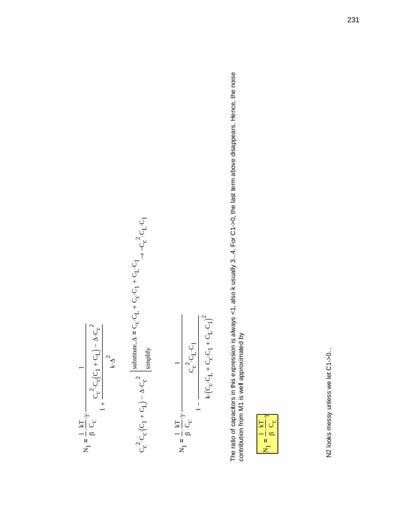
N1
1 βkT C
c⋅
γ⋅1
1C
c2C
cC
1C
L+
()
⋅∆
Cc2
⋅−
k∆
2⋅
+
⋅=
Cc2
Cc
⋅C
1C
L+
()
⋅∆
Cc2
⋅−
subs
titut
e∆
Cc
CL
⋅C
cC
1⋅
+C
LC
1⋅
+=
,
sim
plify
Cc2
−C
L⋅
C1
⋅→
N1
1 βkT C
c⋅
γ⋅1
1C
c2C
L⋅
C1
⋅
kC
cC
L⋅
Cc
C1
⋅+
CL
C1
⋅+
()2
⋅−
⋅=
The
ratio
of c
apac
itors
in th
is e
xpre
ssio
n is
alw
ays
<1, a
lso
k us
ually
3...
4. F
or C
1->0
, the
last
term
abo
ve d
isap
pear
s. H
ence
, the
noi
se
cont
ribut
ion
from
M1
is w
ell a
ppro
xim
ated
by
N1
1 βkT C
c⋅
γ⋅=
N2
look
s m
essy
unl
ess
we
let C
1->0
...
231
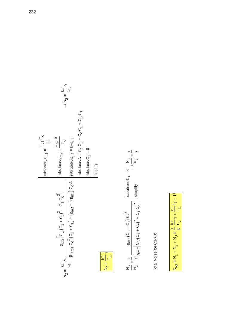
N2
kT CLγ⋅
g m2
CL
C1
Cc
+(
)2⋅
C1
Cc2
⋅+
⎡ ⎣⎤ ⎦
⋅
βg m
1⋅
Cc2
⋅C
1C
L+
()
⋅g m
2β
g m1
⋅−
()C
c⋅
∆⋅+
⋅=
subs
titut
eg m
1ω
c1C
c⋅ β
=,
subs
titut
eg m
2ω
p2∆⋅
Cc
=,
subs
titut
eω
p2kω
c1⋅
=,
subs
titut
e∆
Cc
CL
⋅C
cC
1⋅
+C
LC
1⋅
+=
,
subs
titut
eC
10
=,
sim
plify
N2
kT CLγ⋅
=→
N2
kT CLγ⋅
=
N3
N2
1 γ
g m2
CL
C1
+(
)⋅
Cc2
⋅
g m2
CL
C1
Cc
+(
)2⋅
C1
Cc2
⋅+
⎡ ⎣⎤ ⎦
⋅⋅
=su
bstit
ute
C1
0=
,
sim
plify
N3
N2
1 γ=
→
Tota
l Noi
se fo
r C1-
>0:
Nto
tN
1N
2+
N3
+=
1 βkT C
c⋅
γ⋅kT C
Lγ
1+
()
⋅+
=
232

EE 214 Lecture 20B. Murmann 1
Lecture 20OTA Design Considerations
Boris MurmannStanford University
Copyright © 2007 by Boris Murmann
EE 214 Lecture 20B. Murmann 2
Overview
• Introduction
– Today, we will review a possible design strategy for two-stage OTAs. Since there exist many degrees of freedom in this topology, a thorough hand analysis is essential, and can help minimize, if not completely eliminate, the time needed for a large number of Spice iterations.
233
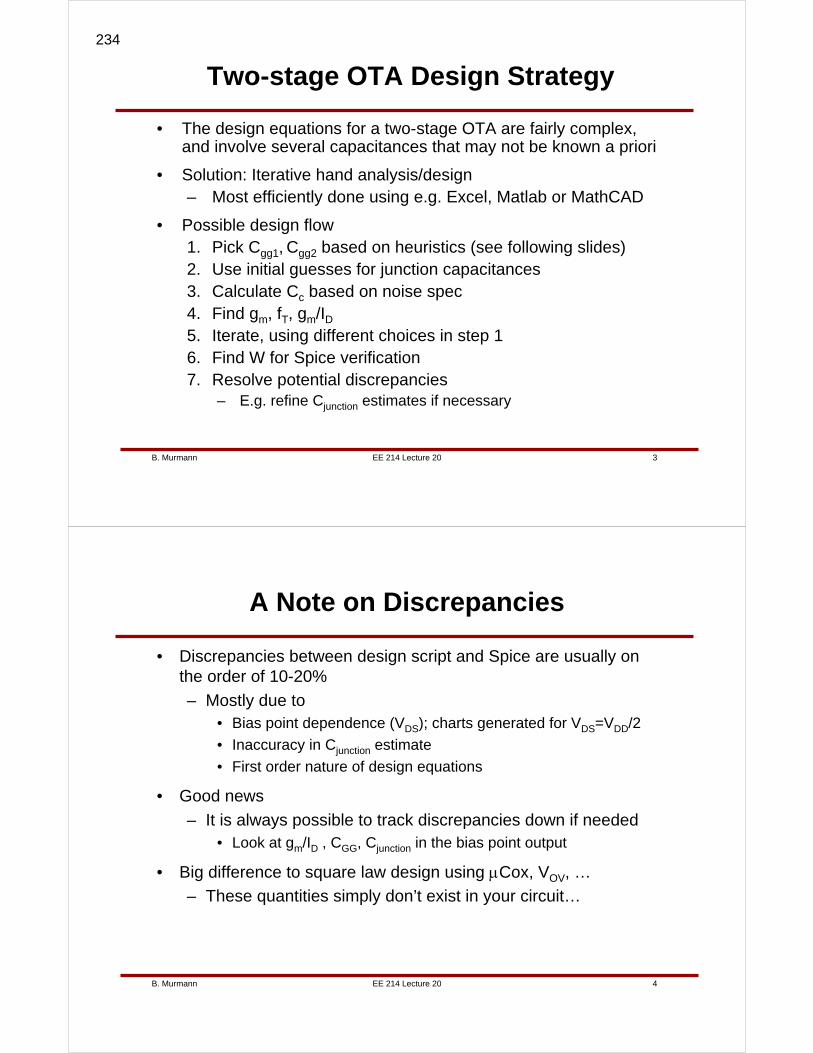
EE 214 Lecture 20B. Murmann 3
Two-stage OTA Design Strategy
• The design equations for a two-stage OTA are fairly complex, and involve several capacitances that may not be known a priori
• Solution: Iterative hand analysis/design– Most efficiently done using e.g. Excel, Matlab or MathCAD
• Possible design flow1. Pick Cgg1, Cgg2 based on heuristics (see following slides) 2. Use initial guesses for junction capacitances3. Calculate Cc based on noise spec4. Find gm, fT, gm/ID5. Iterate, using different choices in step 16. Find W for Spice verification7. Resolve potential discrepancies
– E.g. refine Cjunction estimates if necessary
EE 214 Lecture 20B. Murmann 4
A Note on Discrepancies
• Discrepancies between design script and Spice are usually on the order of 10-20%
– Mostly due to• Bias point dependence (VDS); charts generated for VDS=VDD/2
• Inaccuracy in Cjunction estimate
• First order nature of design equations
• Good news
– It is always possible to track discrepancies down if needed• Look at gm/ID , CGG, Cjunction in the bias point output
• Big difference to square law design using μCox, VOV, …
– These quantities simply don’t exist in your circuit…
234
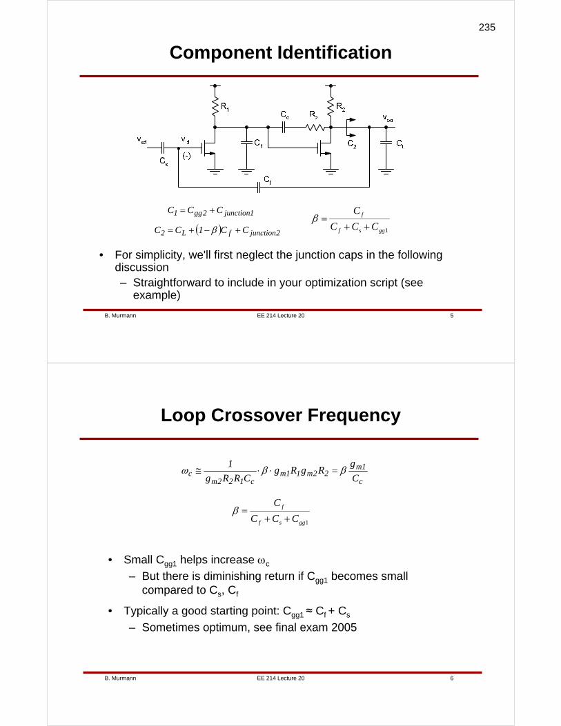
EE 214 Lecture 20B. Murmann 5
Component Identification
1junction2gg1 CCC +=
( ) 2junctionfL2 CC1CC +−+= β 1ggsf
f
CCC
C
++=β
• For simplicity, we'll first neglect the junction caps in the following discussion– Straightforward to include in your optimization script (see
example)
EE 214 Lecture 20B. Murmann 6
Loop Crossover Frequency
• Small Cgg1 helps increase ωc
– But there is diminishing return if Cgg1 becomes small compared to Cs, Cf
• Typically a good starting point: Cgg1 ≈ Cf + Cs
– Sometimes optimum, see final exam 2005
1ggsf
f
CCC
C
++=β
c
1m22m11m
c122mc C
gRgRg
CRRg
1 ββω =⋅⋅≅
235

EE 214 Lecture 20B. Murmann 7
Nondominant Pole
• Heuristic: Start optimization with Cgg2 ≅ CLtot
• For a given ωp2 target and fixed CLtot
– Choosing Cgg2 much smaller than CLtot means excess gm2/Cgg2=ωT2 and therefore small (gm/ID)2
– Choosing Cgg2 much larger than CLtot will cost excess gm2
(power) to meet ωp2 target
Ltotggc
ggLtot
mp
CCC
CCg
++≅
22
22
ω ( ) fLLtot CCC β−+≅ 1
⎟⎟⎟⎟⎟
⎠
⎞
⎜⎜⎜⎜⎜
⎝
⎛+
+⎟⎟⎠
⎞⎜⎜⎝
⎛+≅
c
Ltot2gg
2ggLtot
2m
Ltot
2m
2gg
2p C
CC
CC
1g
C
g
C1
ω
EE 214 Lecture 20B. Murmann 8
Choice of Cc
• In practice, and particularly for high DR designs, Cc is often set by noise requirements
• For designs that are not constraint by noise, it is Interesting to assume Cgg2=CLtot (not necessarily optimum) to develop further qualitative insight
– With this choice, we have ⎟⎟⎠
⎞⎜⎜⎝
⎛+≅
c
Ltot
2T2p C2
C1
21
ωω
• Cc large means that we can use lower ωT2 (higher gm/ID) and save power in the second stage
– But larger Cc also requires larger gm1 and thus more power in the first stage
– This implies that there will be a design-dependent optimum for Cc
236
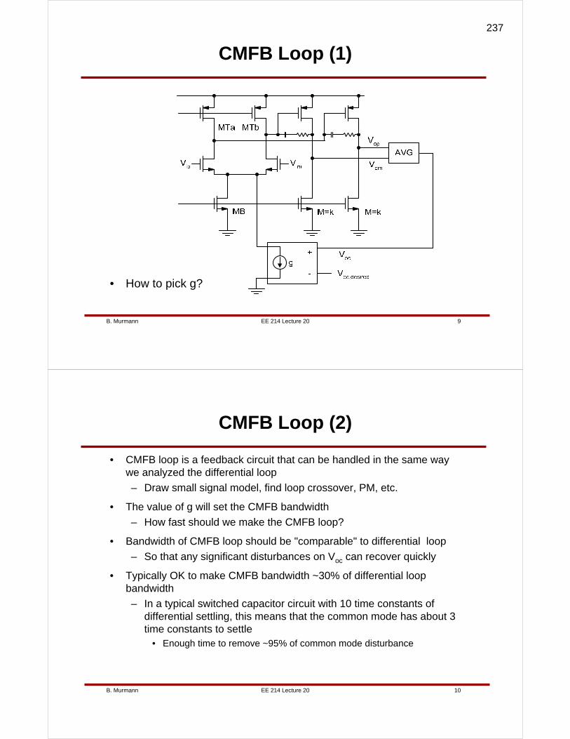
EE 214 Lecture 20B. Murmann 9
CMFB Loop (1)
• How to pick g?
EE 214 Lecture 20B. Murmann 10
CMFB Loop (2)
• CMFB loop is a feedback circuit that can be handled in the same way we analyzed the differential loop
– Draw small signal model, find loop crossover, PM, etc.
• The value of g will set the CMFB bandwidth
– How fast should we make the CMFB loop?
• Bandwidth of CMFB loop should be "comparable" to differential loop
– So that any significant disturbances on Voc can recover quickly
• Typically OK to make CMFB bandwidth ~30% of differential loop bandwidth
– In a typical switched capacitor circuit with 10 time constants of differential settling, this means that the common mode has about 3 time constants to settle
• Enough time to remove ~95% of common mode disturbance
237
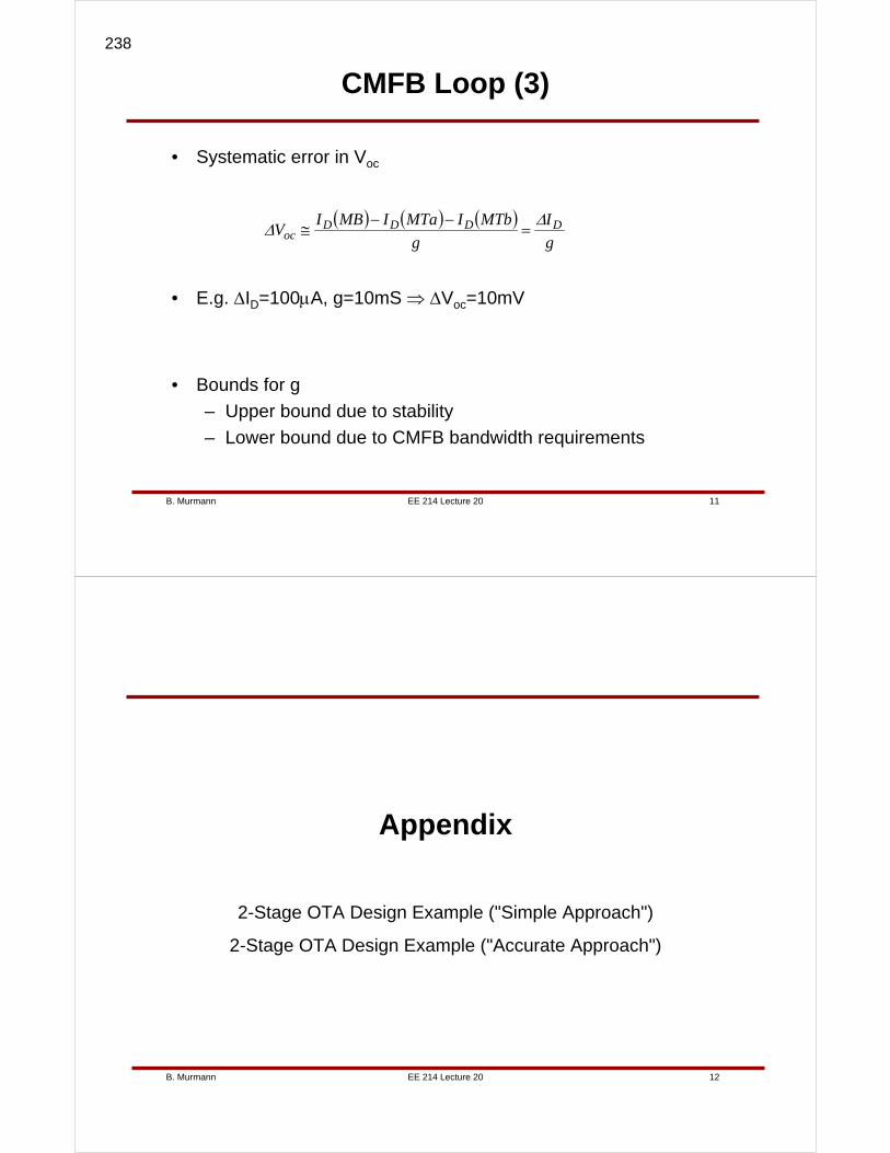
EE 214 Lecture 20B. Murmann 11
CMFB Loop (3)
• Systematic error in Voc
( ) ( ) ( )g
I
g
MTbIMTaIMBIV DDDD
ocΔΔ =
−−≅
• E.g. ΔID=100μA, g=10mS ⇒ ΔVoc=10mV
• Bounds for g
– Upper bound due to stability
– Lower bound due to CMFB bandwidth requirements
EE 214 Lecture 20B. Murmann 12
Appendix
2-Stage OTA Design Example ("Simple Approach")
2-Stage OTA Design Example ("Accurate Approach")
238
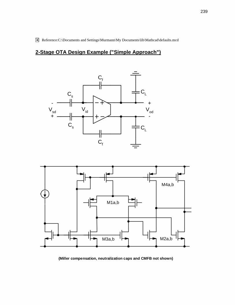
Reference:C:\Documents and Settings\Murmann\My Documents\lib\Mathcad\defaults.mcd
2-Stage OTA Design Example ("Simple Approach")
Cs
-Vsd+
+Vod-
Cs
Cf
Cf
CL
CL
Vid
M1a,b
M2a,bM3a,b
M4a,b
(Miller compensation, neutralization caps and CMFB not shown)
239
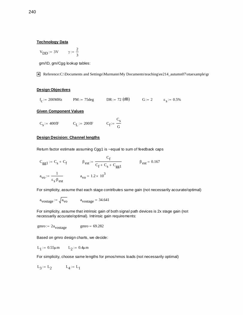
Cgg1 Cs Cf+:= βest
Cf
Cf Cs+ Cgg1+:= βest 0.167=
avo1
εs βest⋅:= avo 1.2 10
3×=
For simplicity, assume that each stage contributes same gain (not necessarily accurate/optimal)
avostage avo:= avostage 34.641=
For simplicity, assume that intrinsic gain of both signal path devices is 2x stage gain (not necessarily accurate/optimal). Intrinsic gain requirements:
gmro 2avostage:= gmro 69.282=
Based on gmro design charts, we decide:
L1 0.55μm:= L2 0.4μm:=
For simplicity, choose same lengths for pmos/nmos loads (not necessarily optimal)
L3 L2:= L4 L1:=
Technology Data
VDD 3V:= γ2
3:=
gm/ID, gm/Cgg lookup tables:
Reference:C:\Documents and Settings\Murmann\My Documents\teaching\ee214_autumn07\otaexample\gm
Design Objectives
fc 200MHz:= PM 75deg:= DR 72:= (dB) G 2:= εs 0.5%:=
Given Component Values
Cs 400fF:= CL 200fF:= Cf
Cs
G:=
Design Decision: Channel lengths
Return factor estimate assuming Cgg1 is ~equal to sum of feedback caps
240
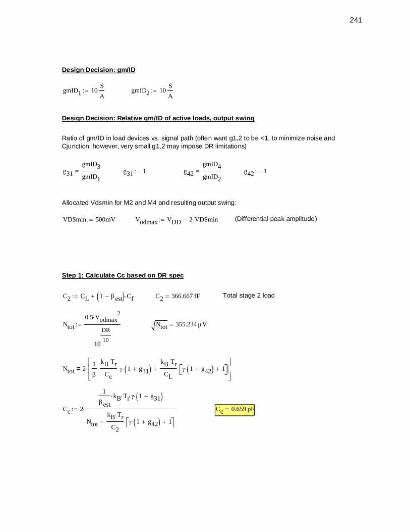
Cc 0.659 pF=Cc 2
1
βestkB⋅ Tr⋅ γ⋅ 1 g31+( )⋅
Ntot
kB Tr⋅
C2γ 1 g42+( )⋅ 1+⎡⎣ ⎤⎦⋅−
⋅:=
Ntot 21
β
kB Tr⋅
Cc⋅ γ⋅ 1 g31+( )⋅
kB Tr⋅
CLγ 1 g42+( )⋅ 1+⎡⎣ ⎤⎦⋅+
⎡⎢⎣
⎤⎥⎦
⋅=
Ntot 355.234 μV=Ntot
0.5 Vodmax2
⋅
10
DR
10
:=
Total stage 2 loadC2 366.667 fF=C2 CL 1 βest−( ) Cf⋅+:=
Step 1: Calculate Cc based on DR spec
(Differential peak amplitude)Vodmax VDD 2 VDSmin⋅−:=VDSmin 500mV:=
Allocated Vdsmin for M2 and M4 and resulting output swing:
g42 1:=g42
gmID4
gmID2=g31 1:=g31
gmID3
gmID1=
Ratio of gm/ID in load devices vs. signal path (often want g1,2 to be <1, to minimize noise and Cjunction; however, very small g1,2 may impose DR limitations)
Design Decision: Relative gm/ID of active loads, output swing
gmID2 10S
A:=gmID1 10
S
A:=
Design Decision: gm/ID
241
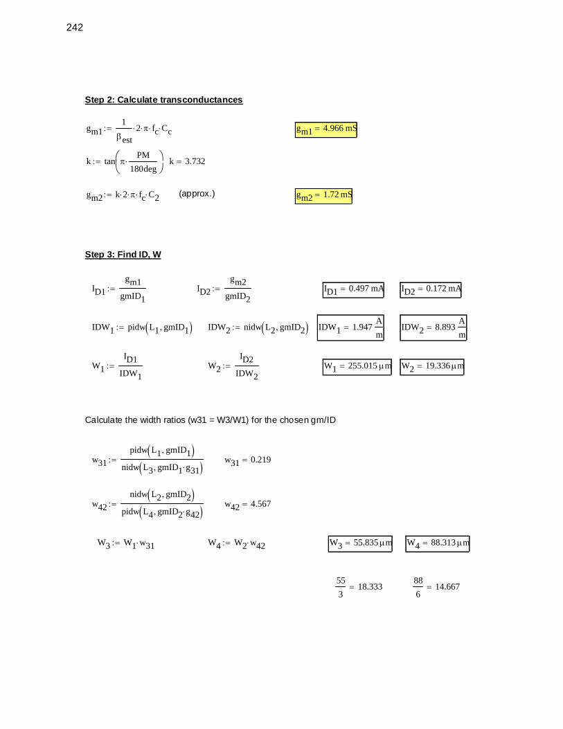
88
614.667=
55
318.333=
W4 88.313 μm=W3 55.835 μm=W4 W2 w42⋅:=W3 W1 w31⋅:=
w42 4.567=w42
nidw L2 gmID2,( )pidw L4 gmID2 g42⋅,( )
:=
w31 0.219=w31
pidw L1 gmID1,( )nidw L3 gmID1 g31⋅,( )
:=
Calculate the width ratios (w31 = W3/W1) for the chosen gm/ID
W2 19.336 μm=W1 255.015 μm=W2
ID2
IDW2:=W1
ID1
IDW1:=
IDW2 8.893A
m=IDW1 1.947
A
m=IDW2 nidw L2 gmID2,( ):=IDW1 pidw L1 gmID1,( ):=
ID2 0.172 mA=ID1 0.497 mA=ID2
gm2
gmID2:=ID1
gm1
gmID1:=
Step 3: Find ID, W
gm2 1.72 mS=(approx.)gm2 k 2⋅ π⋅ fc⋅ C2⋅:=
k 3.732=k tan πPM
180deg⋅⎛⎜
⎝⎞⎟⎠
:=
gm1 4.966 mS=gm11
βest2⋅ π⋅ fc⋅ Cc⋅:=
Step 2: Calculate transconductances
242
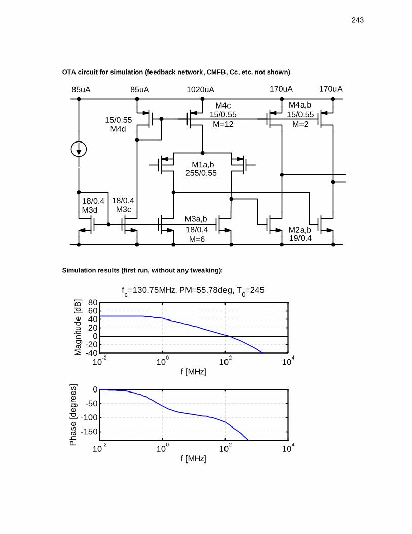
OTA circuit for simulation (feedback network, CMFB, Cc, etc. not shown)
M1a,b
M2a,b
M3a,b
M4a,b
1020uA 170uA 170uA85uA
255/0.55
19/0.4
15/0.55M=215/0.55
15/0.55M=12
18/0.4M=6
85uA
M3d M3c
M4d
M4c
18/0.418/0.4
Simulation results (first run, without any tweaking):
10-2
100
102
104
-40-20
020406080
fc=130.75MHz, PM=55.78deg, T
0=245
f [MHz]
Ma
gn
itud
e [d
B]
10-2
100
102
104
-150
-100
-50
0
f [MHz]
Ph
ase
[de
gre
es]
243
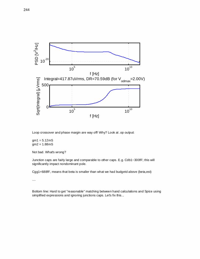
105
1010
10-20
f [Hz]
PS
D [V
2 /Hz]
105
1010
0
500
f [Hz]Sq
rt(I
nte
gra
l) [ μ
Vrm
s] Integral=417.87uVrms, DR=70.59dB (for Vodmax
=2.00V)
Loop crossover and phase margin are way off! Why? Look at .op output:
gm1 = 5.12mSgm2 = 1.88mS
Not bad. What's wrong?
Junction caps are fairly large and comparable to other caps. E.g. Cdb1~300fF; this will significantly impact nondominant pole.
Cgg1=688fF, means that beta is smaller than what we had budgetd above (beta,est)
....
Bottom line: Hard to get "reasonable" matching between hand calculations and Spice using simplified expressions and ignoring junctions caps. Let's fix this...
244
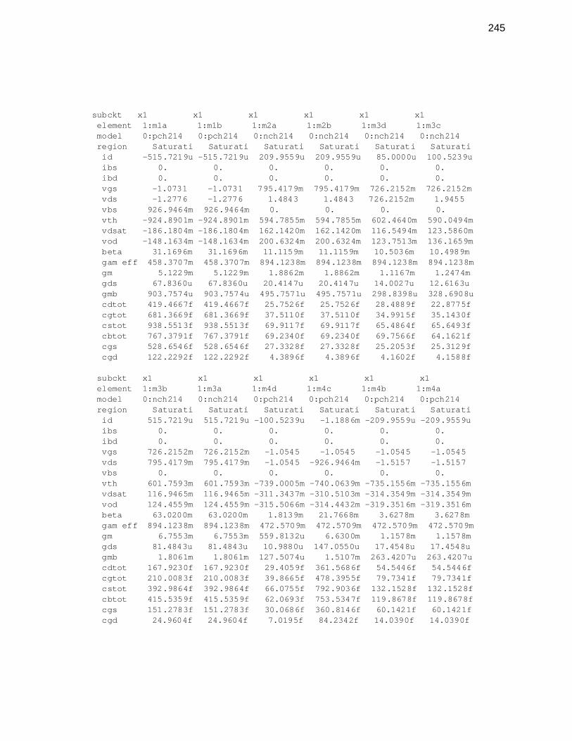
subckt x1 x1 x1 x1 x1 x1 element 1:m1a 1:m1b 1:m2a 1:m2b 1:m3d 1:m3c model 0:pch214 0:pch214 0:nch214 0:nch214 0:nch214 0:nch214 region Saturati Saturati Saturati Saturati Saturati Saturati id -515.7219u -515.7219u 209.9559u 209.9559u 85.0000u 100.5239u ibs 0. 0. 0. 0. 0. 0. ibd 0. 0. 0. 0. 0. 0. vgs -1.0731 -1.0731 795.4179m 795.4179m 726.2152m 726.2152m vds -1.2776 -1.2776 1.4843 1.4843 726.2152m 1.9455 vbs 926.9464m 926.9464m 0. 0. 0. 0. vth -924.8901m -924.8901m 594.7855m 594.7855m 602.4640m 590.0494m vdsat -186.1804m -186.1804m 162.1420m 162.1420m 116.5494m 123.5860m vod -148.1634m -148.1634m 200.6324m 200.6324m 123.7513m 136.1659m beta 31.1696m 31.1696m 11.1159m 11.1159m 10.5036m 10.4989m gam eff 458.3707m 458.3707m 894.1238m 894.1238m 894.1238m 894.1238m gm 5.1229m 5.1229m 1.8862m 1.8862m 1.1167m 1.2474m gds 67.8360u 67.8360u 20.4147u 20.4147u 14.0027u 12.6163u gmb 903.7574u 903.7574u 495.7571u 495.7571u 298.8398u 328.6908u cdtot 419.4667f 419.4667f 25.7526f 25.7526f 28.4889f 22.8775f cgtot 681.3669f 681.3669f 37.5110f 37.5110f 34.9915f 35.1430f cstot 938.5513f 938.5513f 69.9117f 69.9117f 65.4864f 65.6493f cbtot 767.3791f 767.3791f 69.2340f 69.2340f 69.7566f 64.1621f cgs 528.6546f 528.6546f 27.3328f 27.3328f 25.2053f 25.3129f cgd 122.2292f 122.2292f 4.3896f 4.3896f 4.1602f 4.1588f
subckt x1 x1 x1 x1 x1 x1 element 1:m3b 1:m3a 1:m4d 1:m4c 1:m4b 1:m4a model 0:nch214 0:nch214 0:pch214 0:pch214 0:pch214 0:pch214 region Saturati Saturati Saturati Saturati Saturati Saturati id 515.7219u 515.7219u -100.5239u -1.1886m -209.9559u -209.9559u ibs 0. 0. 0. 0. 0. 0. ibd 0. 0. 0. 0. 0. 0. vgs 726.2152m 726.2152m -1.0545 -1.0545 -1.0545 -1.0545 vds 795.4179m 795.4179m -1.0545 -926.9464m -1.5157 -1.5157 vbs 0. 0. 0. 0. 0. 0. vth 601.7593m 601.7593m -739.0005m -740.0639m -735.1556m -735.1556m vdsat 116.9465m 116.9465m -311.3437m -310.5103m -314.3549m -314.3549m vod 124.4559m 124.4559m -315.5066m -314.4432m -319.3516m -319.3516m beta 63.0200m 63.0200m 1.8139m 21.7668m 3.6278m 3.6278m gam eff 894.1238m 894.1238m 472.5709m 472.5709m 472.5709m 472.5709m gm 6.7553m 6.7553m 559.8132u 6.6300m 1.1578m 1.1578m gds 81.4843u 81.4843u 10.9880u 147.0550u 17.4548u 17.4548u gmb 1.8061m 1.8061m 127.5074u 1.5107m 263.4207u 263.4207u cdtot 167.9230f 167.9230f 29.4059f 361.5686f 54.5446f 54.5446f cgtot 210.0083f 210.0083f 39.8665f 478.3955f 79.7341f 79.7341f cstot 392.9864f 392.9864f 66.0755f 792.9036f 132.1528f 132.1528f cbtot 415.5359f 415.5359f 62.0693f 753.5347f 119.8678f 119.8678f cgs 151.2783f 151.2783f 30.0686f 360.8146f 60.1421f 60.1421f cgd 24.9604f 24.9604f 7.0195f 84.2342f 14.0390f 14.0390f
245
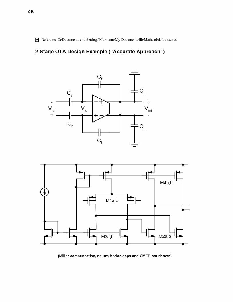
Reference:C:\Documents and Settings\Murmann\My Documents\lib\Mathcad\defaults.mcd
2-Stage OTA Design Example ("Accurate Approach")
Cs
-Vsd+
+Vod-
Cs
Cf
Cf
CL
CL
Vid
M1a,b
M2a,bM3a,b
M4a,b
(Miller compensation, neutralization caps and CMFB not shown)
246
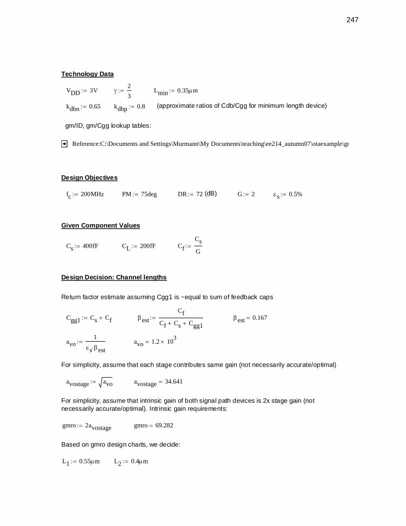
CL 200fF:= Cf
Cs
G:=
Design Decision: Channel lengths
Return factor estimate assuming Cgg1 is ~equal to sum of feedback caps
Cgg1 Cs Cf+:= βest
Cf
Cf Cs+ Cgg1+:= βest 0.167=
avo1
εs βest⋅:= avo 1.2 10
3×=
For simplicity, assume that each stage contributes same gain (not necessarily accurate/optimal)
avostage avo:= avostage 34.641=
For simplicity, assume that intrinsic gain of both signal path devices is 2x stage gain (not necessarily accurate/optimal). Intrinsic gain requirements:
gmro 2avostage:= gmro 69.282=
Based on gmro design charts, we decide:
L1 0.55μm:= L2 0.4μm:=
Technology Data
VDD 3V:= γ2
3:= Lmin 0.35μm:=
kdbn 0.65:= kdbp 0.8:= (approximate ratios of Cdb/Cgg for minimum length device)
gm/ID, gm/Cgg lookup tables:
Reference:C:\Documents and Settings\Murmann\My Documents\teaching\ee214_autumn07\otaexample\gm
Design Objectives
fc 200MHz:= PM 75deg:= DR 72:= (dB) G 2:= εs 0.5%:=
Given Component Values
Cs 400fF:=
247
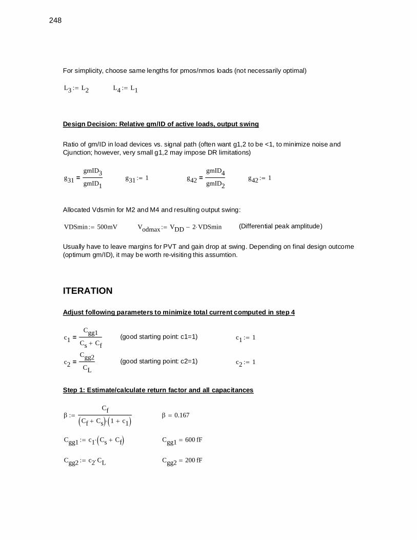
Cgg2 200 fF=Cgg2 c2 CL⋅:=
Cgg1 600 fF=Cgg1 c1 Cs Cf+( )⋅:=
β 0.167=βCf
Cf Cs+( ) 1 c1+( )⋅:=
Step 1: Estimate/calculate return factor and all capacitances
c2 1:=(good starting point: c2=1)c2
Cgg2
CL=
c1 1:=(good starting point: c1=1)c1
Cgg1
Cs Cf+=
Adjust following parameters to minimize total current computed in step 4
ITERATION
Usually have to leave margins for PVT and gain drop at swing. Depending on final design outcome (optimum gm/ID), it may be worth re-visiting this assumtion.
(Differential peak amplitude)Vodmax VDD 2 VDSmin⋅−:=VDSmin 500mV:=
Allocated Vdsmin for M2 and M4 and resulting output swing:
g42 1:=g42
gmID4
gmID2=g31 1:=g31
gmID3
gmID1=
Ratio of gm/ID in load devices vs. signal path (often want g1,2 to be <1, to minimize noise and Cjunction; however, very small g1,2 may impose DR limitations)
Design Decision: Relative gm/ID of active loads, output swing
L4 L1:=L3 L2:=
For simplicity, choose same lengths for pmos/nmos loads (not necessarily optimal)
248
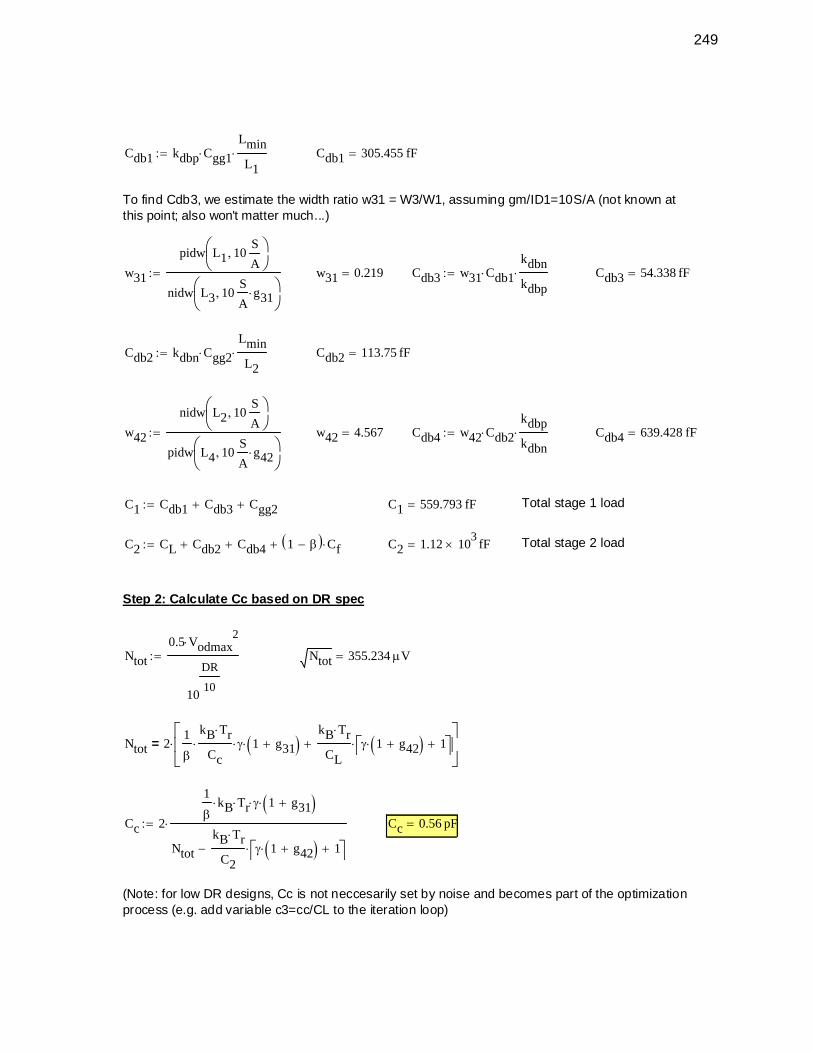
(Note: for low DR designs, Cc is not neccesarily set by noise and becomes part of the optimization process (e.g. add variable c3=cc/CL to the iteration loop)
Cc 0.56 pF=Cc 2
1
βkB⋅ Tr⋅ γ⋅ 1 g31+( )⋅
Ntot
kB Tr⋅
C2γ 1 g42+( )⋅ 1+⎡⎣ ⎤⎦⋅−
⋅:=
Ntot 21
β
kB Tr⋅
Cc⋅ γ⋅ 1 g31+( )⋅
kB Tr⋅
CLγ 1 g42+( )⋅ 1+⎡⎣ ⎤⎦⋅+
⎡⎢⎣
⎤⎥⎦
⋅=
Ntot 355.234 μV=Ntot
0.5 Vodmax2
⋅
10
DR
10
:=
Step 2: Calculate Cc based on DR spec
Total stage 2 loadC2 1.12 103
× fF=C2 CL Cdb2+ Cdb4+ 1 β−( ) Cf⋅+:=
Total stage 1 loadC1 559.793 fF=C1 Cdb1 Cdb3+ Cgg2+:=
Cdb4 639.428 fF=Cdb4 w42 Cdb2⋅kdbp
kdbn⋅:=w42 4.567=w42
nidw L2 10S
A,⎛⎜
⎝⎞⎟⎠
pidw L4 10S
Ag42⋅,⎛⎜
⎝⎞⎟⎠
:=
Cdb2 113.75 fF=Cdb2 kdbn Cgg2⋅Lmin
L2⋅:=
Cdb3 54.338 fF=Cdb3 w31 Cdb1⋅kdbn
kdbp⋅:=w31 0.219=w31
pidw L1 10S
A,⎛⎜
⎝⎞⎟⎠
nidw L3 10S
Ag31⋅,⎛⎜
⎝⎞⎟⎠
:=
To find Cdb3, we estimate the width ratio w31 = W3/W1, assuming gm/ID1=10S/A (not known at this point; also won't matter much...)
Cdb1 305.455 fF=Cdb1 kdbp Cgg1⋅Lmin
L1⋅:=
249
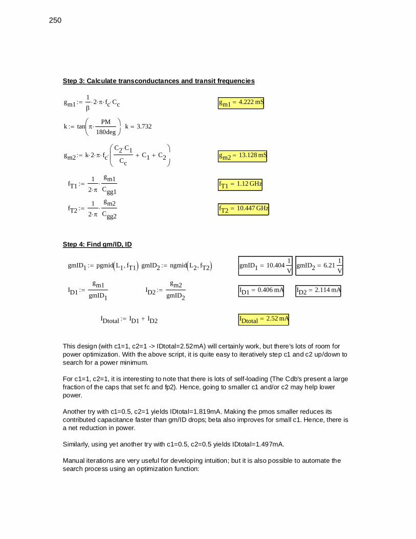
This design (with c1=1, c2=1 -> IDtotal=2.52mA) will certainly work, but there's lots of room for power optimization. With the above script, it is quite easy to iteratively step c1 and c2 up/down to search for a power minimum.
For c1=1, c2=1, it is interesting to note that there is lots of self-loading (The Cdb's present a large fraction of the caps that set fc and fp2). Hence, going to smaller c1 and/or c2 may help lower power.
Another try with c1=0.5, c2=1 yields IDtotal=1.819mA. Making the pmos smaller reduces its contributed capacitance faster than gm/ID drops; beta also improves for small c1. Hence, there is a net reduction in power.
Similarly, using yet another try with c1=0.5, c2=0.5 yields IDtotal=1.497mA.
Manual iterations are very useful for developing intuition; but it is also possible to automate the search process using an optimization function:
IDtotal 2.52 mA=IDtotal ID1 ID2+:=
ID2 2.114 mA=ID1 0.406 mA=ID2
gm2
gmID2:=ID1
gm1
gmID1:=
gmID2 6.211
V=gmID1 10.404
1
V=gmID2 ngmid L2 fT2,( ):=gmID1 pgmid L1 fT1,( ):=
Step 4: Find gm/ID, ID
fT2 10.447 GHz=fT21
2 π⋅
gm2
Cgg2⋅:=
fT1 1.12 GHz=fT11
2 π⋅
gm1
Cgg1⋅:=
gm2 13.128 mS=gm2 k 2⋅ π⋅ fc⋅C2 C1⋅
CcC1+ C2+
⎛⎜⎝
⎞⎟⎠
⋅:=
k 3.732=k tan πPM
180deg⋅⎛⎜
⎝⎞⎟⎠
:=
gm1 4.222 mS=gm11
β2⋅ π⋅ fc⋅ Cc⋅:=
Step 3: Calculate transconductances and transit frequencies
250
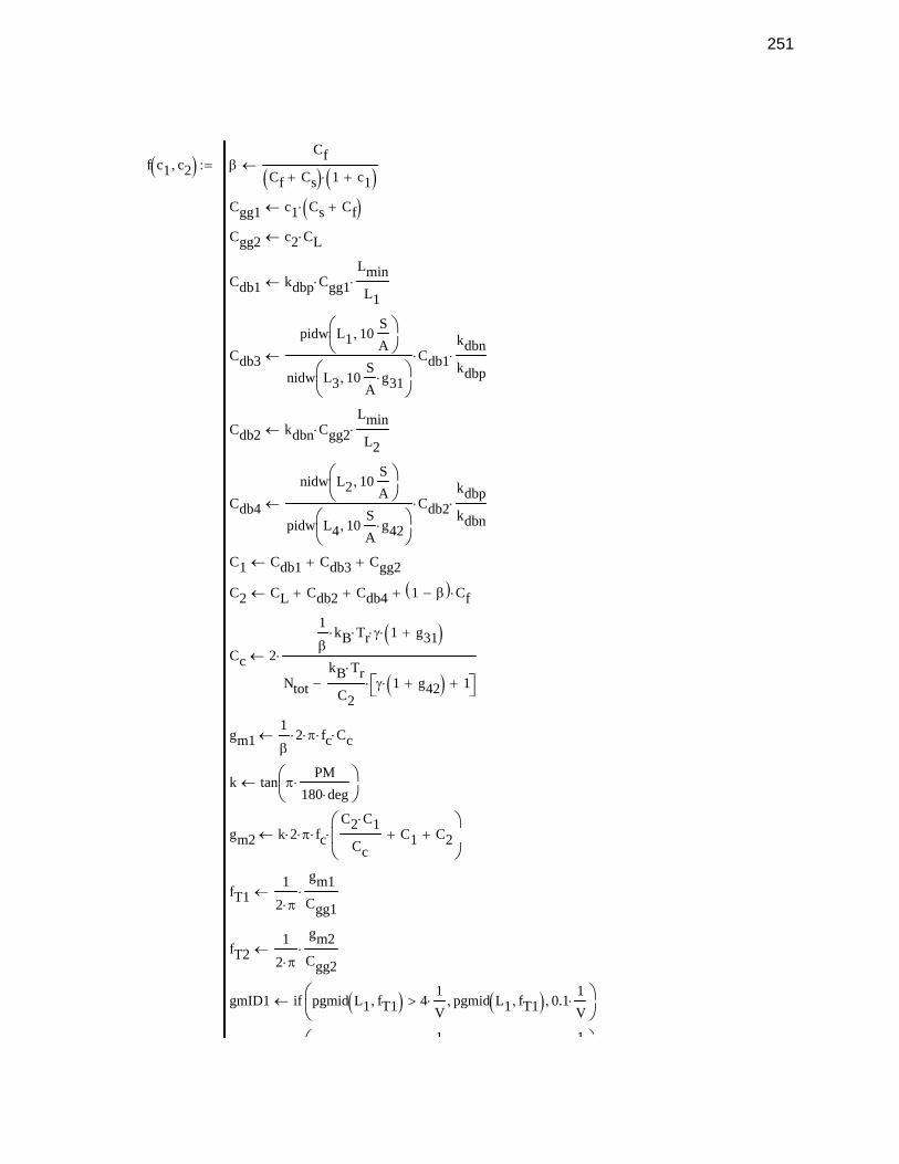
f c1 c2,( ) βCf
Cf Cs+( ) 1 c1+( )⋅←
Cgg1 c1 Cs Cf+( )⋅←
Cgg2 c2 CL⋅←
Cdb1 kdbp Cgg1⋅Lmin
L1⋅←
Cdb3
pidw L1 10S
A,⎛⎜
⎝⎞⎟⎠
nidw L3 10S
Ag31⋅,⎛⎜
⎝⎞⎟⎠
Cdb1⋅kdbn
kdbp⋅←
Cdb2 kdbn Cgg2⋅Lmin
L2⋅←
Cdb4
nidw L2 10S
A,⎛⎜
⎝⎞⎟⎠
pidw L4 10S
Ag42⋅,⎛⎜
⎝⎞⎟⎠
Cdb2⋅kdbp
kdbn⋅←
C1 Cdb1 Cdb3+ Cgg2+←
C2 CL Cdb2+ Cdb4+ 1 β−( ) Cf⋅+←
Cc 2
1
βkB⋅ Tr⋅ γ⋅ 1 g31+( )⋅
Ntot
kB Tr⋅
C2γ 1 g42+( )⋅ 1+⎡⎣ ⎤⎦⋅−
⋅←
gm11
β2⋅ π⋅ fc⋅ Cc⋅←
k tan πPM
180 deg⋅⋅⎛⎜
⎝⎞⎟⎠
←
gm2 k 2⋅ π⋅ fc⋅C2 C1⋅
CcC1+ C2+
⎛⎜⎝
⎞⎟⎠
⋅←
fT11
2 π⋅
gm1
Cgg1⋅←
fT21
2 π⋅
gm2
Cgg2⋅←
gmID1 if pgmid L1 fT1,( ) 41
V⋅> pgmid L1 fT1,( ), 0.1
1
V⋅,⎛⎜
⎝⎞⎟⎠
←
1 1⎛ ⎞
:=
251
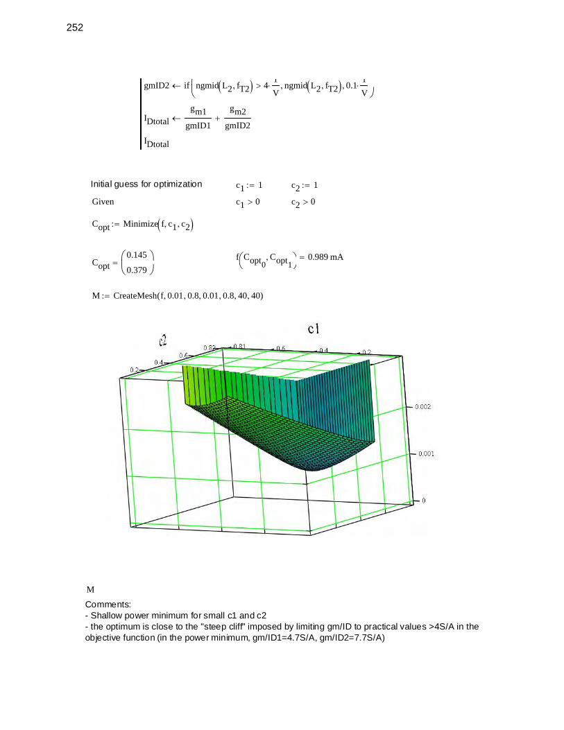
gmID2 if ngmid L2 fT2,( ) 41
V⋅> ngmid L2 fT2,( ), 0.1
1
V⋅,⎛⎜
⎝⎞⎟⎠
←
IDtotal
gm1
gmID1
gm2
gmID2+←
IDtotal
Initial guess for optimization c1 1:= c2 1:=
Given c1 0> c2 0>
Copt Minimize f c1, c2,( ):=
f Copt0Copt1,⎛
⎝⎞⎠
0.989 mA=Copt
0.145
0.379
⎛⎜⎝
⎞⎟⎠
=
M CreateMesh f 0.01, 0.8, 0.01, 0.8, 40, 40,( ):=
M
Comments:- Shallow power minimum for small c1 and c2- the optimum is close to the "steep cliff" imposed by limiting gm/ID to practical values >4S/A in the objective function (in the power minimum, gm/ID1=4.7S/A, gm/ID2=7.7S/A)
252
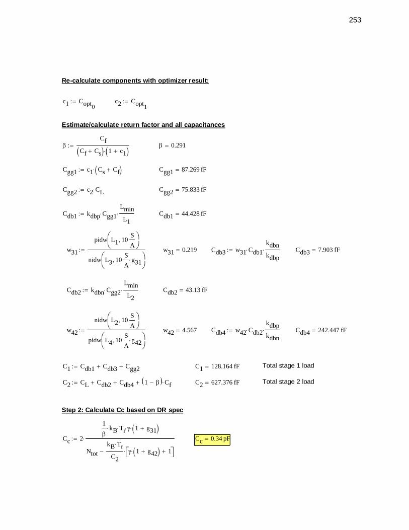
Cc 0.34 pF=Cc 2
1
βkB⋅ Tr⋅ γ⋅ 1 g31+( )⋅
Ntot
kB Tr⋅
C2γ 1 g42+( )⋅ 1+⎡⎣ ⎤⎦⋅−
⋅:=
Step 2: Calculate Cc based on DR spec
Total stage 2 loadC2 627.376 fF=C2 CL Cdb2+ Cdb4+ 1 β−( ) Cf⋅+:=
Total stage 1 loadC1 128.164 fF=C1 Cdb1 Cdb3+ Cgg2+:=
Cdb4 242.447 fF=Cdb4 w42 Cdb2⋅kdbp
kdbn⋅:=w42 4.567=w42
nidw L2 10S
A,⎛⎜
⎝⎞⎟⎠
pidw L4 10S
Ag42⋅,⎛⎜
⎝⎞⎟⎠
:=
Cdb2 43.13 fF=Cdb2 kdbn Cgg2⋅Lmin
L2⋅:=
Cdb3 7.903 fF=Cdb3 w31 Cdb1⋅kdbn
kdbp⋅:=w31 0.219=w31
pidw L1 10S
A,⎛⎜
⎝⎞⎟⎠
nidw L3 10S
Ag31⋅,⎛⎜
⎝⎞⎟⎠
:=
Cdb1 44.428 fF=Cdb1 kdbp Cgg1⋅Lmin
L1⋅:=
Cgg2 75.833 fF=Cgg2 c2 CL⋅:=
Cgg1 87.269 fF=Cgg1 c1 Cs Cf+( )⋅:=
β 0.291=βCf
Cf Cs+( ) 1 c1+( )⋅:=
Estimate/calculate return factor and all capacitances
c2 Copt1:=c1 Copt0
:=
Re-calculate components with optimizer result:
253
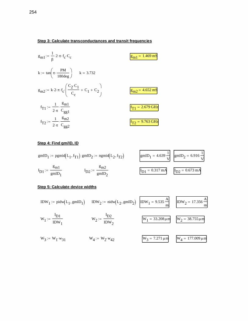
W4 177.009 μm=W3 7.271 μm=W4 W2 w42⋅:=W3 W1 w31⋅:=
W2 38.755 μm=W1 33.208 μm=W2
ID2
IDW2:=W1
ID1
IDW1:=
IDW2 17.356A
m=IDW1 9.535
A
m=IDW2 nidw L2 gmID2,( ):=IDW1 pidw L1 gmID1,( ):=
Step 5: Calculate device widths
ID2 0.673 mA=ID1 0.317 mA=ID2
gm2
gmID2:=
Step 3: Calculate transconductances and transit frequencies
gm11
β2⋅ π⋅ fc⋅ Cc⋅:= gm1 1.469 mS=
k tan πPM
180deg⋅⎛⎜
⎝⎞⎟⎠
:= k 3.732=
gm2 k 2⋅ π⋅ fc⋅C2 C1⋅
CcC1+ C2+
⎛⎜⎝
⎞⎟⎠
⋅:= gm2 4.652 mS=
fT11
2 π⋅
gm1
Cgg1⋅:= fT1 2.679 GHz=
fT21
2 π⋅
gm2
Cgg2⋅:= fT2 9.763 GHz=
Step 4: Find gm/ID, ID
gmID1 pgmid L1 fT1,( ):= gmID2 ngmid L2 fT2,( ):= gmID1 4.6391
V= gmID2 6.916
1
V=
ID1
gm1
gmID1:=
254
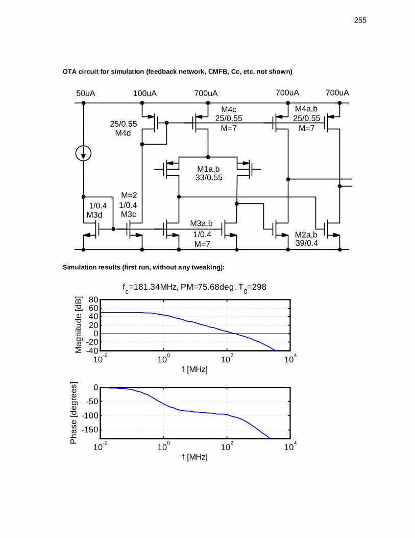
OTA circuit for simulation (feedback network, CMFB, Cc, etc. not shown)
M1a,b
M2a,b
M3a,b
M4a,b
700uA 700uA 700uA100uA
33/0.55
39/0.4
25/0.55M=725/0.55
25/0.55M=7
1/0.4M=7
50uA
M3d M3c
M4d
M4c
1/0.41/0.4M=2
Simulation results (first run, without any tweaking):
10-2
100
102
104
-40-20
020406080
fc=181.34MHz, PM=75.68deg, T
0=298
f [MHz]
Ma
gn
itud
e [d
B]
10-2
100
102
104
-150
-100
-50
0
f [MHz]
Ph
ase
[de
gre
es]
255
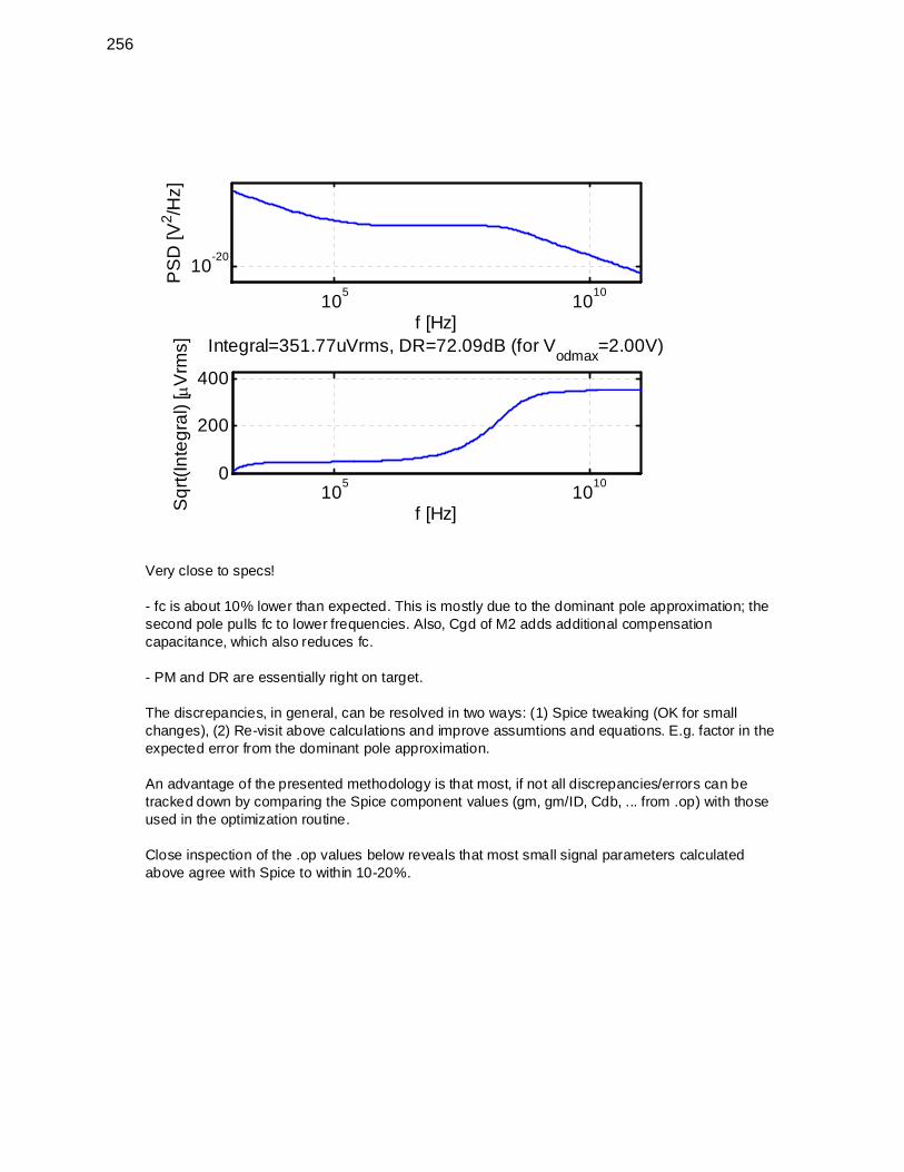
105
1010
10-20
f [Hz]
PS
D [V
2 /Hz]
105
1010
0
200
400
f [Hz]Sq
rt(I
nte
gra
l) [ μ
Vrm
s] Integral=351.77uVrms, DR=72.09dB (for Vodmax
=2.00V)
Very close to specs!
- fc is about 10% lower than expected. This is mostly due to the dominant pole approximation; the second pole pulls fc to lower frequencies. Also, Cgd of M2 adds additional compensation capacitance, which also reduces fc.
- PM and DR are essentially right on target.
The discrepancies, in general, can be resolved in two ways: (1) Spice tweaking (OK for small changes), (2) Re-visit above calculations and improve assumtions and equations. E.g. factor in the expected error from the dominant pole approximation.
An advantage of the presented methodology is that most, if not all discrepancies/errors can be tracked down by comparing the Spice component values (gm, gm/ID, Cdb, ... from .op) with those used in the optimization routine.
Close inspection of the .op values below reveals that most small signal parameters calculated above agree with Spice to within 10-20%.
256
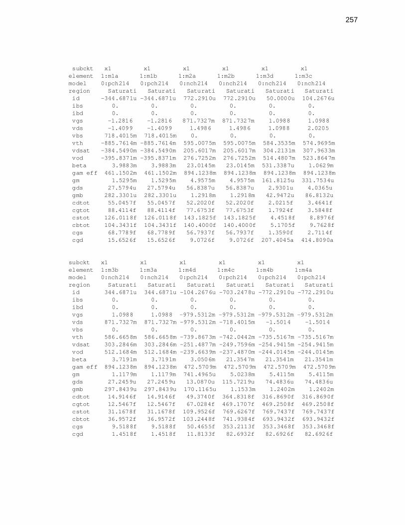
subckt x1 x1 x1 x1 x1 x1 element 1:m1a 1:m1b 1:m2a 1:m2b 1:m3d 1:m3c model 0:pch214 0:pch214 0:nch214 0:nch214 0:nch214 0:nch214 region Saturati Saturati Saturati Saturati Saturati Saturati id -344.6871u -344.6871u 772.2910u 772.2910u 50.0000u 104.2676u ibs 0. 0. 0. 0. 0. 0. ibd 0. 0. 0. 0. 0. 0. vgs -1.2816 -1.2816 871.7327m 871.7327m 1.0988 1.0988 vds -1.4099 -1.4099 1.4986 1.4986 1.0988 2.0205 vbs 718.4015m 718.4015m 0. 0. 0. 0. vth -885.7614m -885.7614m 595.0075m 595.0075m 584.3535m 574.9695m vdsat -384.5490m -384.5490m 205.6017m 205.6017m 304.2131m 307.9633m vod -395.8371m -395.8371m 276.7252m 276.7252m 514.4807m 523.8647m beta 3.9883m 3.9883m 23.0145m 23.0145m 531.3387u 1.0629m gam eff 461.1502m 461.1502m 894.1238m 894.1238m 894.1238m 894.1238m gm 1.5295m 1.5295m 4.9575m 4.9575m 161.8125u 331.7534u gds 27.5794u 27.5794u 56.8387u 56.8387u 2.9301u 4.0365u gmb 282.3301u 282.3301u 1.2918m 1.2918m 42.9472u 86.8132u cdtot 55.0457f 55.0457f 52.2020f 52.2020f 2.0215f 3.4641f cgtot 88.4114f 88.4114f 77.6753f 77.6753f 1.7924f 3.5848f cstot 126.0118f 126.0118f 143.1825f 143.1825f 4.4518f 8.8976f cbtot 104.3431f 104.3431f 140.4000f 140.4000f 5.1705f 9.7628f cgs 68.7789f 68.7789f 56.7937f 56.7937f 1.3590f 2.7114f cgd 15.6526f 15.6526f 9.0726f 9.0726f 207.4045a 414.8090a
subckt x1 x1 x1 x1 x1 x1 element 1:m3b 1:m3a 1:m4d 1:m4c 1:m4b 1:m4a model 0:nch214 0:nch214 0:pch214 0:pch214 0:pch214 0:pch214 region Saturati Saturati Saturati Saturati Saturati Saturati id 344.6871u 344.6871u -104.2676u -703.2478u -772.2910u -772.2910u ibs 0. 0. 0. 0. 0. 0. ibd 0. 0. 0. 0. 0. 0. vgs 1.0988 1.0988 -979.5312m -979.5312m -979.5312m -979.5312m vds 871.7327m 871.7327m -979.5312m -718.4015m -1.5014 -1.5014 vbs 0. 0. 0. 0. 0. 0. vth 586.6658m 586.6658m -739.8673m -742.0442m -735.5167m -735.5167m vdsat 303.2846m 303.2846m -251.4877m -249.7596m -254.9415m -254.9415m vod 512.1684m 512.1684m -239.6639m -237.4870m -244.0145m -244.0145m beta 3.7191m 3.7191m 3.0506m 21.3547m 21.3541m 21.3541m gam eff 894.1238m 894.1238m 472.5709m 472.5709m 472.5709m 472.5709m gm 1.1179m 1.1179m 741.4965u 5.0238m 5.4115m 5.4115m gds 27.2459u 27.2459u 13.0870u 115.7219u 74.4836u 74.4836u gmb 297.8439u 297.8439u 170.1165u 1.1533m 1.2402m 1.2402m cdtot 14.9146f 14.9146f 49.3740f 364.8318f 316.8690f 316.8690f cgtot 12.5467f 12.5467f 67.0284f 469.1707f 469.2508f 469.2508f cstot 31.1678f 31.1678f 109.9526f 769.6267f 769.7437f 769.7437f cbtot 36.9572f 36.9572f 103.2448f 741.9384f 693.9432f 693.9432f cgs 9.5188f 9.5188f 50.4655f 353.2113f 353.3468f 353.3468f cgd 1.4518f 1.4518f 11.8133f 82.6932f 82.6926f 82.6926f
257
EE 214 Lecture 21B. Murmann 1
Lecture 21Step Response
Boris MurmannStanford University
Copyright © 2007 by Boris Murmann
EE 214 Lecture 21B. Murmann 2
Overview
• Reading
– 7.5 (Relation Between Frequency and Time Response)
• Reference
– H.C. Yang and D.J. Allstot, "Considerations for fast settling operational amplifiers," IEEE Trans. Ckts. and Syst., March 1990, pp. 326 – 334.
• Introduction
– OTAs with capacitive feedback are primarily used in switched capacitor circuits, where fast settling to voltage steps at the input is critical. In today's lecture we will look at first and second order behavior in the step response of feedback OTAs.
258
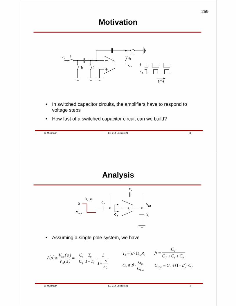
EE 214 Lecture 21B. Murmann 3
Motivation
• In switched capacitor circuits, the amplifiers have to respond to voltage steps
• How fast of a switched capacitor circuit can we build?
EE 214 Lecture 21B. Murmann 4
Analysis
• Assuming a single pole system, we have
( )
c
0
0
f
s
in
out
s1
1
T1
T
C
C
)s(V
)s(VsA
ω+
⋅+
−=≅
Ltot
mc C
G⋅≅ βω
insf
f
CCC
C
++=β
omRGT ⋅= β0
( ) fLLtot CCC ⋅−+= β1
259
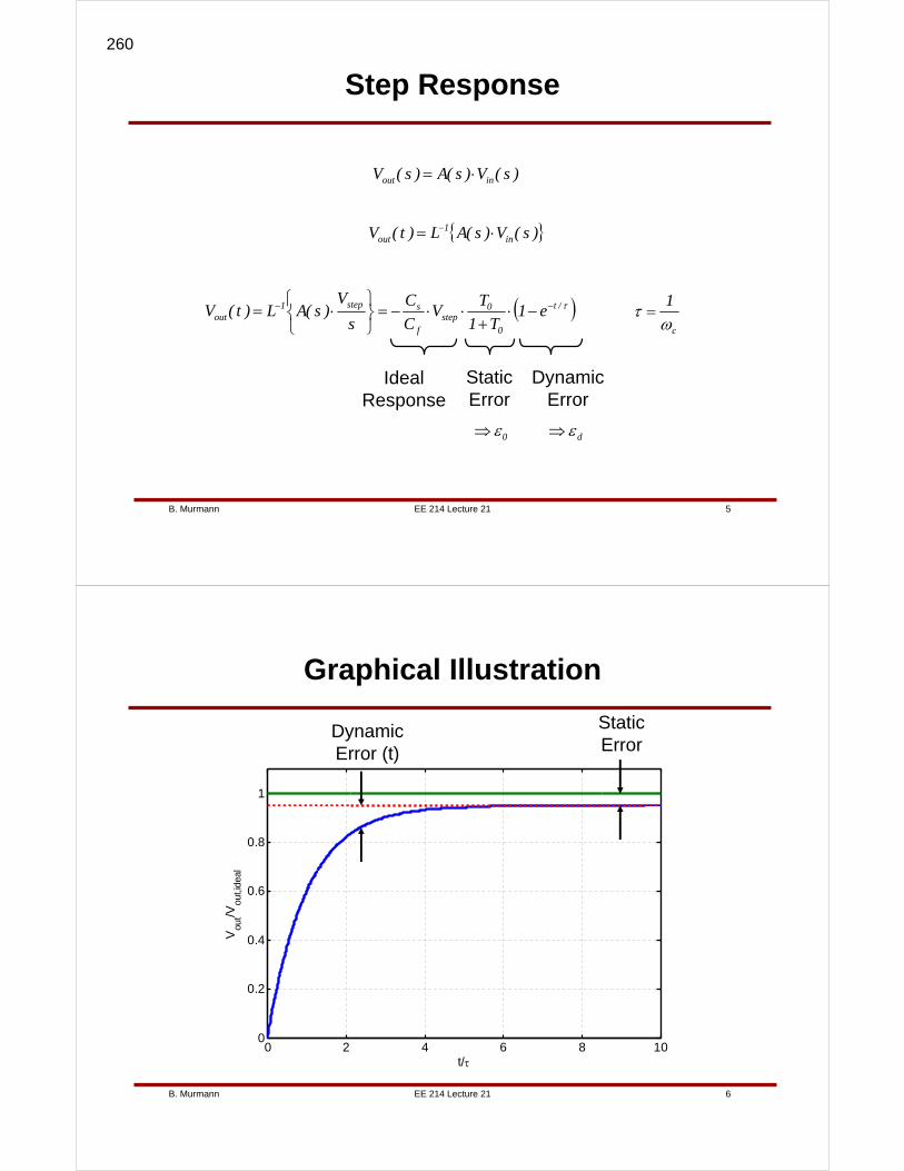
EE 214 Lecture 21B. Murmann 5
Step Response
)s(V)s(A)s(V inout ⋅=
)s(V)s(AL)t(V in1
out ⋅= −
( )τ/t
0
0step
f
sstep1out e1
T1
TV
C
C
s
V)s(AL)t(V −− −⋅
+⋅⋅−=
⎭⎬⎫
⎩⎨⎧
⋅=c
1
ωτ =
Ideal Response
Static Error
Dynamic Error
0ε⇒ dε⇒
EE 214 Lecture 21B. Murmann 6
0 2 4 6 8 100
0.2
0.4
0.6
0.8
1
t/τ
Vou
t/Vou
t,ide
al
Graphical Illustration
Dynamic Error (t)
Static Error
260
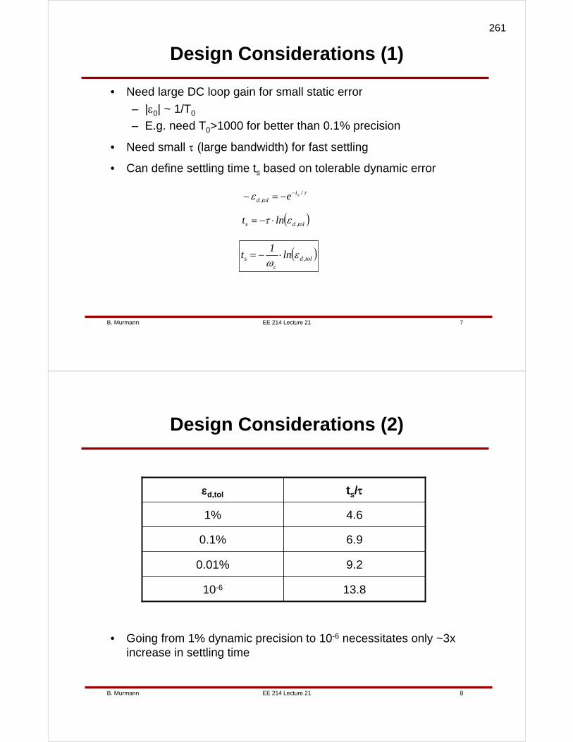
EE 214 Lecture 21B. Murmann 7
Design Considerations (1)
• Need large DC loop gain for small static error
– |ε0| ~ 1/T0
– E.g. need T0>1000 for better than 0.1% precision
• Need small τ (large bandwidth) for fast settling
• Can define settling time ts based on tolerable dynamic error
τε /ttol,d
se−−=−
( )tol,ds lnt ετ ⋅−=
( )tol,dc
s ln1
t εω
⋅−=
EE 214 Lecture 21B. Murmann 8
Design Considerations (2)
• Going from 1% dynamic precision to 10-6 necessitates only ~3x increase in settling time
9.20.01%
13.810-6
6.90.1%
4.61%
ts/τεd,tol
261

EE 214 Lecture 21B. Murmann 9
Design Considerations (3)
2.90.01%
4.410-6
2.20.1%
1.51%
fc/fCLKε
• A switched capacitor circuit operates in two clock phases
• Fitting the required number of time constants within ½ period lets us relate fCLK to a minimum bandwidth requirement
( )CLK
max,dc
s f
1
2
1ln
f2
1t <⋅
⋅−= ε
π( )max,d
CLK
c ln1
f
f επ
−>
EE 214 Lecture 21B. Murmann 10
How Fast Can We Go?
• fc cannot be larger than about 1/3 of the nondominant amplifier pole frequency (stability)
– In a cascoded amplifier, the nondominant pole occurs at a frequency around fT/3
• Assuming that two junction caps equal to Cgg are present
– At a reasonable bias, the NMOS transit frequency in our technology is roughly 8GHz (nominal process and temperature)
• Putting all of this together, and assuming that we'll need to settle to within 0.01% (~9 time constants), we have
MHz26630
f
9
f
9.2
1f TT
max,CLK =≅⋅=
262
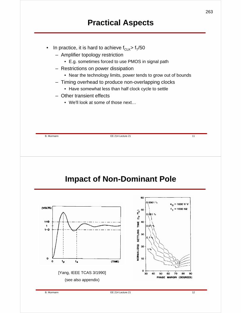
EE 214 Lecture 21B. Murmann 11
Practical Aspects
• In practice, it is hard to achieve fCLK> fT/50
– Amplifier topology restriction• E.g. sometimes forced to use PMOS in signal path
– Restrictions on power dissipation• Near the technology limits, power tends to grow out of bounds
– Timing overhead to produce non-overlapping clocks• Have somewhat less than half clock cycle to settle
– Other transient effects• We'll look at some of those next…
EE 214 Lecture 21B. Murmann 12
Impact of Non-Dominant Pole
[Yang, IEEE TCAS 3/1990]
(see also appendix)
263
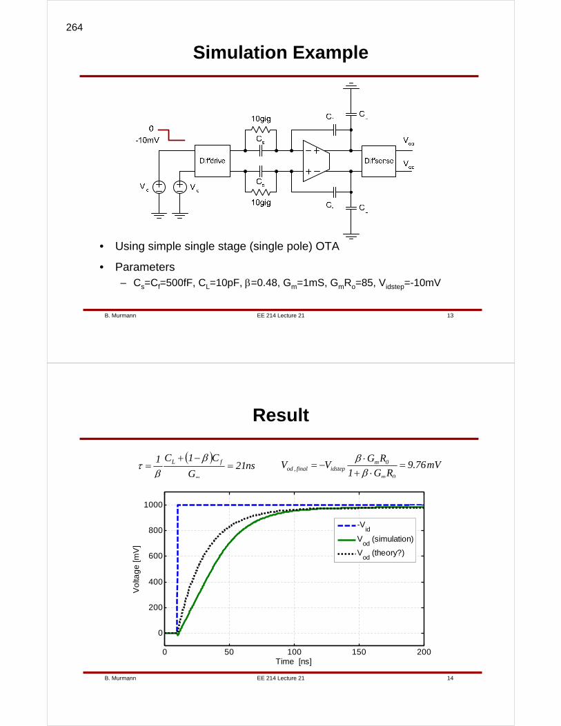
EE 214 Lecture 21B. Murmann 13
Simulation Example
• Using simple single stage (single pole) OTA
• Parameters– Cs=Cf=500fF, CL=10pF, β=0.48, Gm=1mS, GmRo=85, Vidstep=-10mV
EE 214 Lecture 21B. Murmann 14
Result
( )ns21
G
C1C1
m
fL =−+
=β
βτ mV76.9
RG1
RGVV
0m
0midstepfinal,od =
⋅+⋅
−=β
β
0 50 100 150 200
0
200
400
600
800
1000
Time [ns]
Vo
ltag
e [m
V]
-Vid
Vod
(simulation)
Vod
(theory?)
264
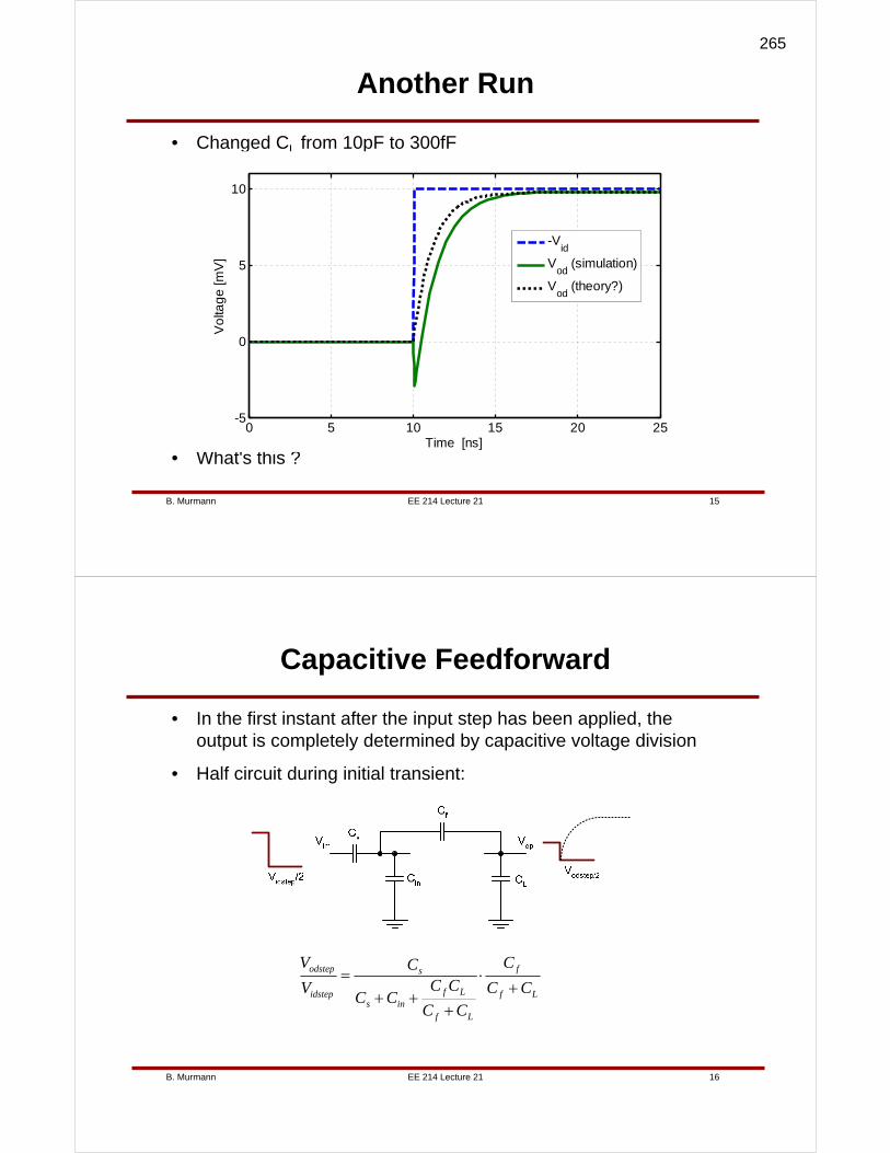
EE 214 Lecture 21B. Murmann 15
Another Run
• Changed CL from 10pF to 300fF
• What's this ?
0 5 10 15 20 25-5
0
5
10
Time [ns]
Vo
ltag
e [m
V]
-Vid
Vod
(simulation)
Vod
(theory?)
EE 214 Lecture 21B. Murmann 16
Capacitive Feedforward
• In the first instant after the input step has been applied, the output is completely determined by capacitive voltage division
• Half circuit during initial transient:
Lf
f
Lf
Lfins
s
idstep
odstep
CC
C
CC
CCCC
C
V
V
+⋅
+++
=
265
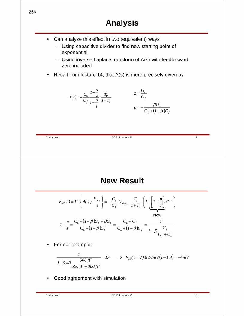
EE 214 Lecture 21B. Murmann 17
Analysis
• Can analyze this effect in two (equivalent) ways
– Using capacitive divider to find new starting point of exponential
– Using inverse Laplace transform of A(s) with feedforward zero included
• Recall from lecture 14, that A(s) is more precisely given by
( )0
0
f
s
T1
T
p
s1
z
s1
C
CsA
+⋅
−
−−= f
m
C
Gz =
( ) fL
m
C1C
Gp
ββ−+
−=
EE 214 Lecture 21B. Murmann 18
New Result
• For our example:
⎟⎟⎠
⎞⎜⎜⎝
⎛⎥⎦⎤
⎢⎣⎡ −−⋅
+⋅⋅−=
⎭⎬⎫
⎩⎨⎧
⋅= −− τ/t
0
0idstep
f
sstep1od e
z
p11
T1
TV
C
C
s
V)s(AL)t(V
New
( )( ) ( )
Lf
ffL
fL
fL
ffL
CC
C1
1
C1C
CC
C1C
CC1C
z
p1
+−
=−+
+=
−+
+−+=−
βββββ
( ) mV44.11mV10)0t(V4.1
fF300fF500fF500
48.01
1od −=−≅=⇒=
+−
• Good agreement with simulation
266

EE 214 Lecture 21B. Murmann 19
New Settling Time
• Settling time for given precision increases due to feedforward, since the settling range is artificially enlarged
• E.g. in our simulation example, the time to settle within 0.1% dynamic error increases from 6.9τ to 7.3τ– Not extremely significant, especially when β is low and CL is
at least comparable to Cf
⎟⎟⎠
⎞⎜⎜⎝
⎛
⎥⎥⎦
⎤
⎢⎢⎣
⎡
+⋅−⋅−=
Lf
ftol,d
cs CC
C1ln
1t βε
ω
<1
EE 214 Lecture 21B. Murmann 20
Appendix
"Bandwidth and Settling of a Two-Pole Feedback Amplifier"
267

ts τ− ln εd( )⋅=εd e
ts
τ−
=Dynamic error at t=ts
τ1
ωc1=u t( ) 1 e
t
τ−
−=Step response:
Linear settling time
ω3dB ωc1=T jω3dB( )
1 T jω3dB( )+
1
2=
1
1ω3dB
ωc1
⎛⎜⎜⎝
⎞⎟⎟⎠
2
+
1
2=
1
1 jω3dB
ωc1+
1
2=
Closed loop 3-dB frequency (neglecting feedforward effects)
PM1 90deg:=PM1 180deg arg1
jωc1
ωc1
⎛⎜⎜⎜⎝
⎞⎟⎟⎟⎠
+=
Phase margin
ωc1 βGm
C⋅=
1
j ωc1⋅C
β Gm⋅⋅
1=
Unity gain frequency of T(s)
For large DC loop gain: T s( )1
sC
β Gm⋅⋅
=
T s( )β Gm⋅ R⋅
1 sRC+=
1
1
β Gm⋅ R⋅s
C
β Gm⋅⋅+
=T s( )β T0⋅
1s
p1−
=
Single Pole Amplifier (for reference) Boris Murmann11/11/2006
Bandwidth and Settling of a Two-Pole Feedback Amplifier
268
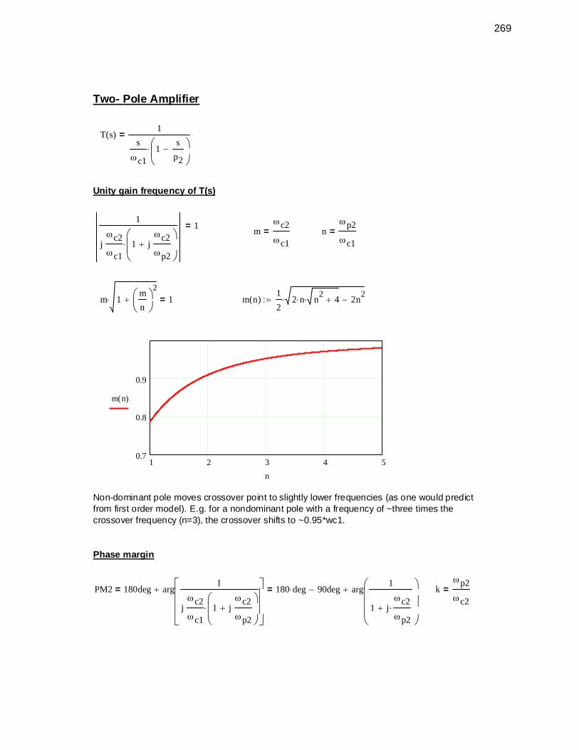
Two- Pole Amplifier
T s( )1
s
ωc11
s
p2−⎛
⎜⎝
⎞⎟⎠
⋅
=
Unity gain frequency of T(s)
1
jωc2
ωc11 j
ωc2
ωp2+
⎛⎜⎜⎝
⎞⎟⎟⎠
⋅
1=m
ωc2
ωc1= n
ωp2
ωc1=
m 1m
n⎛⎜⎝
⎞⎟⎠
2
+⋅ 1= m n( )1
22 n⋅ n
24+⋅ 2n
2−⋅:=
1 2 3 4 50.7
0.8
0.9
m n( )
n
Non-dominant pole moves crossover point to slightly lower frequencies (as one would predict from first order model). E.g. for a nondominant pole with a frequency of ~three times the crossover frequency (n=3), the crossover shifts to ~0.95*wc1.
Phase margin
PM2 180deg arg1
jωc2
ωc11 j
ωc2
ωp2+
⎛⎜⎜⎝
⎞⎟⎟⎠
⋅
⎡⎢⎢⎢⎣
⎤⎥⎥⎥⎦
+= 180 deg⋅ 90deg− arg1
1 jωc2
ωp2⋅+
⎛⎜⎜⎜⎝
⎞⎟⎟⎟⎠
+= kωp2
ωc2=
269

PM2 k( ) 90deg atan1
k⎛⎜⎝
⎞⎟⎠
−:=
1 2 3 4 5 6 7 840
50
60
70
80
90
PM2 k( )180
π⋅
k
k PM2( )1
tanπ
2PM2−⎛⎜
⎝⎞⎟⎠
:=
45 50 55 60 65 70 75 801
2
3
4
5
6
k PMπ
180⋅⎛⎜
⎝⎞⎟⎠
PM
270
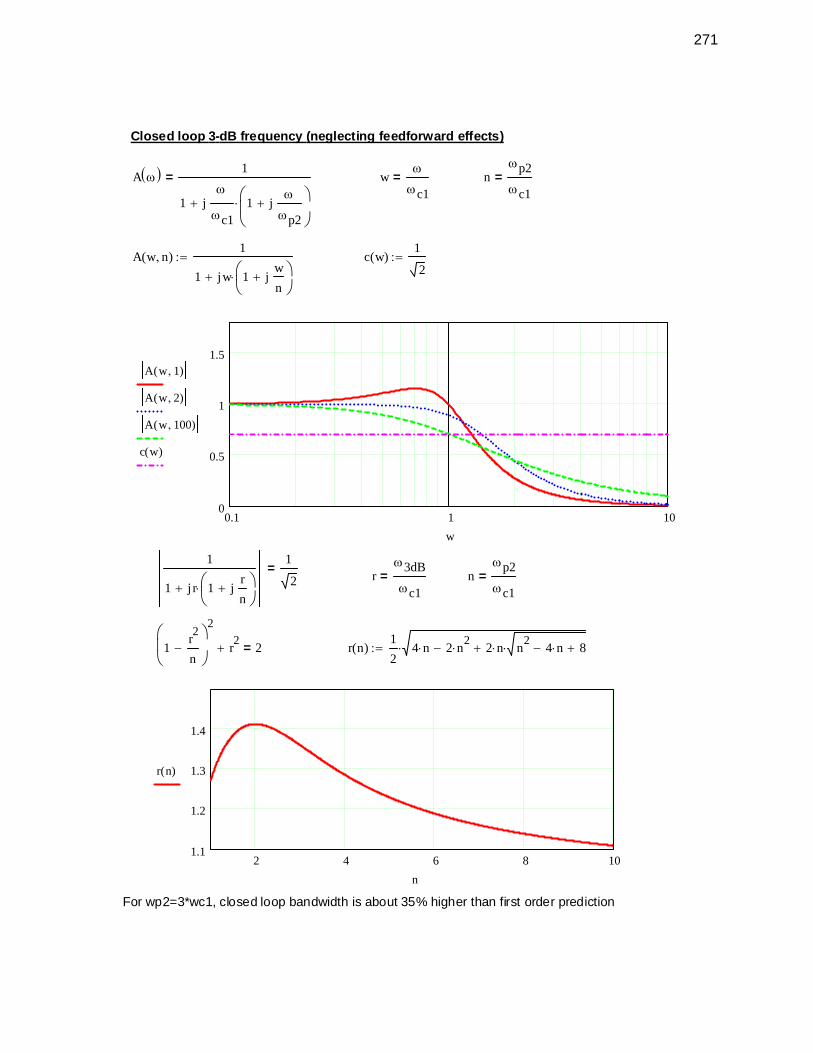
Closed loop 3-dB frequency (neglecting feedforward effects)
A ω( ) 1
1 jω
ωc11 j
ω
ωp2+⎛
⎜⎝
⎞⎟⎠
⋅+
= wω
ωc1= n
ωp2
ωc1=
A w n,( )1
1 jw 1 jw
n+⎛⎜
⎝⎞⎟⎠
⋅+
:= c w( )1
2:=
0.1 1 100
0.5
1
1.5A w 1,( )
A w 2,( )
A w 100,( )
c w( )
w
1
1 j r 1 jr
n+⎛⎜
⎝⎞⎟⎠
⋅+
1
2=
rω3dB
ωc1= n
ωp2
ωc1=
1r2
n−
⎛⎜⎝
⎞⎟⎠
2
r2
+ 2= r n( )1
24 n⋅ 2 n
2⋅− 2 n⋅ n
24 n⋅− 8+⋅+⋅:=
2 4 6 8 101.1
1.2
1.3
1.4
r n( )
n
For wp2=3*wc1, closed loop bandwidth is about 35% higher than first order prediction
271
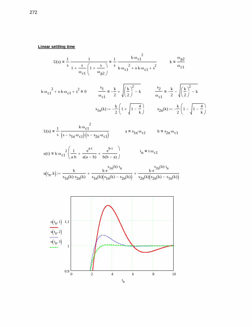
Linear settling time
U s( ) =U s( )
1
s
1
1s
ωc11
s
ωp2+⎛
⎜⎝
⎞⎟⎠
⋅+
⋅=1
s
k ωc12
⋅
k ωc12
⋅ s k⋅ ωc1⋅+ s2
+
⋅= kωp2
ωc1=
k ωc12
⋅ s k⋅ ωc1⋅+ s2
+ 0=s1
ωc1
k
2−
k
2⎛⎜⎝
⎞⎟⎠
2
k−+=s2
ωc1
k
2−
k
2⎛⎜⎝
⎞⎟⎠
2
k−−=
s1n k( )k
2− 1 1
4
k−+
⎛⎜⎝
⎞⎟⎠
⋅:= s2n k( )k
2− 1 1
4
k−−
⎛⎜⎝
⎞⎟⎠
⋅:=
U s( )1
s
k ωc12
⋅
s s1n ωc1⋅−( ) s s2n ωc1⋅−( )⋅⋅= a s1n ωc1⋅= b s2n ωc1⋅=
tn t ωc1⋅=u t( ) k ωc1
2⋅
1
a b⋅
ea t⋅
a a b−( )+
eb t⋅
b b a−( )+
⎛⎜⎝
⎞⎟⎠
⋅=
u tn k,( ) k
s1n k( ) s2n k( )⋅
k es1n k( ) tn⋅
⋅
s1n k( ) s1n k( ) s2n k( )−( )+
k es2n k( ) tn⋅
⋅
s2n k( ) s2n k( ) s1n k( )−( )+:=
0 2 4 6 8 100.9
1
1.1u tn 1,( )u tn 2,( )u tn 3,( )
tn
272
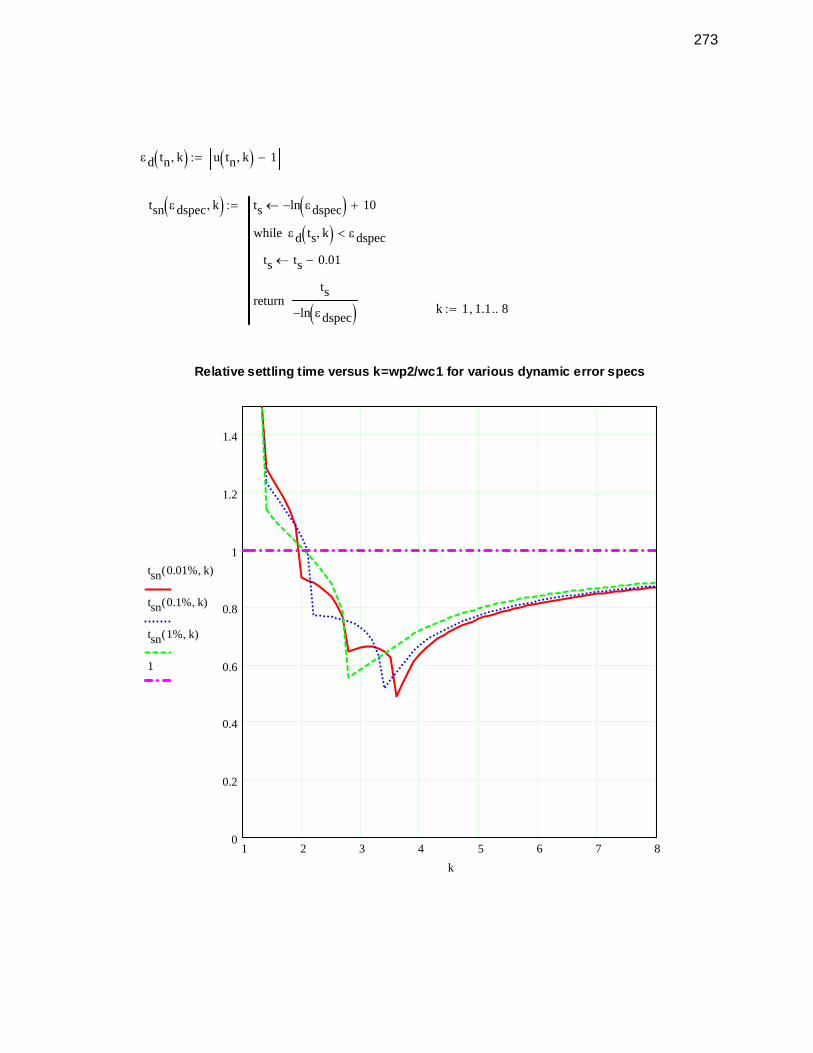
εd tn k,( ) u tn k,( ) 1−:=
tsn εdspec k,( ) ts ln εdspec( )− 10+←
ts ts 0.01−←
εd ts k,( ) εdspec<while
ts
ln εdspec( )−return
:=
k 1 1.1, 8..:=
Relative settling time versus k=wp2/wc1 for various dynamic error specs
1 2 3 4 5 6 7 80
0.2
0.4
0.6
0.8
1
1.2
1.4
tsn 0.01% k,( )
tsn 0.1% k,( )
tsn 1% k,( )
1
k
273
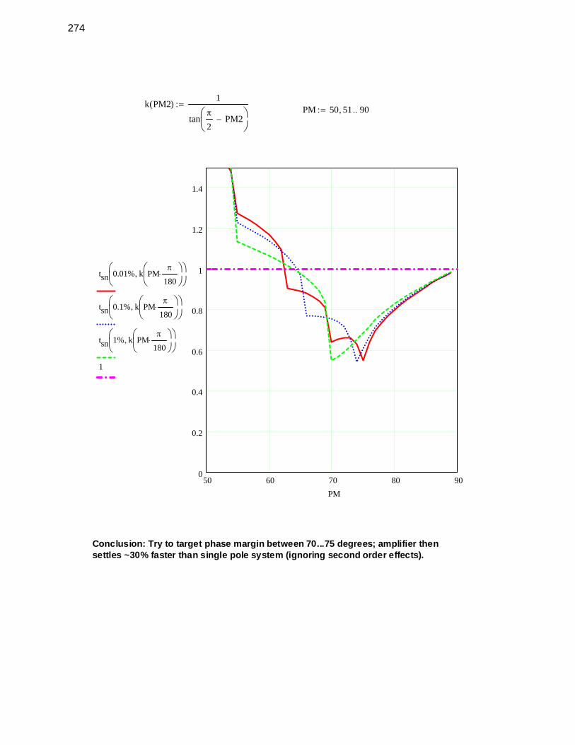
k PM2( )1
tanπ
2PM2−⎛⎜
⎝⎞⎟⎠
:=PM 50 51, 90..:=
50 60 70 80 900
0.2
0.4
0.6
0.8
1
1.2
1.4
tsn 0.01% k PMπ
180⋅⎛⎜
⎝⎞⎟⎠
,⎛⎜⎝
⎞⎟⎠
tsn 0.1% k PMπ
180⋅⎛⎜
⎝⎞⎟⎠
,⎛⎜⎝
⎞⎟⎠
tsn 1% k PMπ
180⋅⎛⎜
⎝⎞⎟⎠
,⎛⎜⎝
⎞⎟⎠
1
PM
Conclusion: Try to target phase margin between 70...75 degrees; amplifier then settles ~30% faster than single pole system (ignoring second order effects).
274

EE 214 Lecture 22B. Murmann 1
Lecture 22Slewing
Boris MurmannStanford University
Copyright © 2007 by Boris Murmann
EE 214 Lecture 22B. Murmann 2
Overview
• Reading
– 9.6.1, 9.6.2, 9.6.5 (Slew Rate)
• Introduction
– Today we'll complete our discussion of transient behavior in OTA circuits with capacitive feedback. Aside from the feedforward artifact we've discovered last time, there exists another effect called "slewing". Whenever the differential input pair is driven outside its "linear range", the differential output current is limited by the available tail bias. In typicalswitched capacitor circuits, slewing can cause a significant speed reduction, and is therefore an important effect to consider.
275
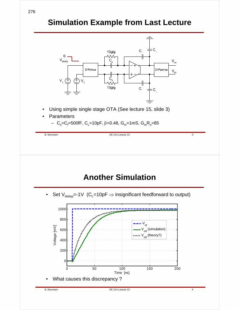
EE 214 Lecture 22B. Murmann 3
Simulation Example from Last Lecture
• Using simple single stage OTA (See lecture 15, slide 3)
• Parameters– Cs=Cf=500fF, CL=10pF, β=0.48, Gm=1mS, GmRo=85
EE 214 Lecture 22B. Murmann 4
Another Simulation
• Set Vidstep=-1V (CL=10pF ⇒ insignificant feedforward to output)
• What causes this discrepancy ?
0 50 100 150 200
0
200
400
600
800
1000
Time [ns]
Vo
ltag
e [m
V]
-Vid
Vod
(simulation)
Vod
(theory?)
276
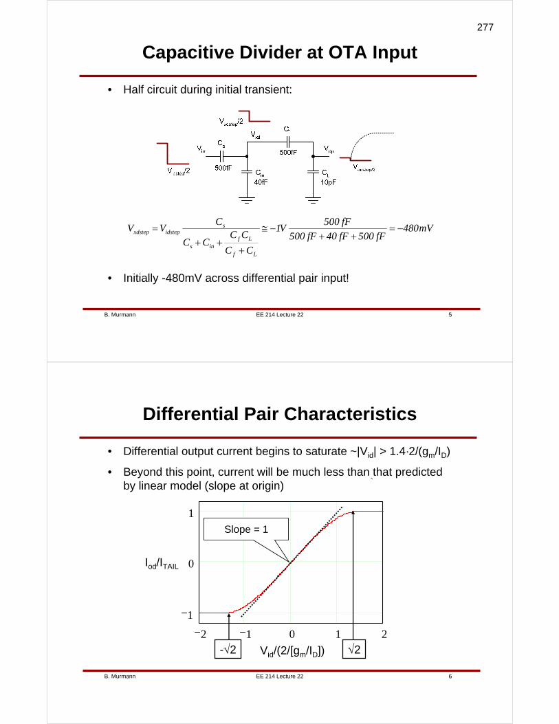
EE 214 Lecture 22B. Murmann 5
Capacitive Divider at OTA Input
• Half circuit during initial transient:
mV480fF500fF40fF500
fF500V1
CC
CCCC
CVV
Lf
Lfins
sidstepxdstep −=
++−≅
+++
=
• Initially -480mV across differential pair input!
EE 214 Lecture 22B. Murmann 6
Differential Pair Characteristics
• Differential output current begins to saturate ~|Vid| > 1.4·2/(gm/ID)
• Beyond this point, current will be much less than that predictedby linear model (slope at origin)
Iod/ITAIL
⎝
2 1 0 1 2
1
0
1
Slope = 1
Vid/(2/[gm/ID])-√2 √2
277
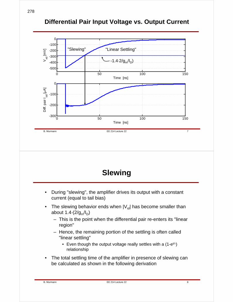
EE 214 Lecture 22B. Murmann 7
0 50 100 150
-500
-400
-300
-200
-100
0
Time [ns]
Vxd
[mV
]
0 50 100 150-300
-200
-100
0
Time [ns]
Diff
. pa
ir I od
[ μA
]
Differential Pair Input Voltage vs. Output Current
-1.4·2/gm/ID)
"Slewing" "Linear Settling"
EE 214 Lecture 22B. Murmann 8
Slewing
• During "slewing", the amplifier drives its output with a constant current (equal to tail bias)
• The slewing behavior ends when |Vid| has become smaller than about 1.4·(2/gm/ID)
– This is the point when the differential pair re-enters its "linear region"
– Hence, the remaining portion of the settling is often called "linear settling"
• Even though the output voltage really settles with a (1-et/τ) relationship
• The total settling time of the amplifier in presence of slewing can be calculated as shown in the following derivation
278
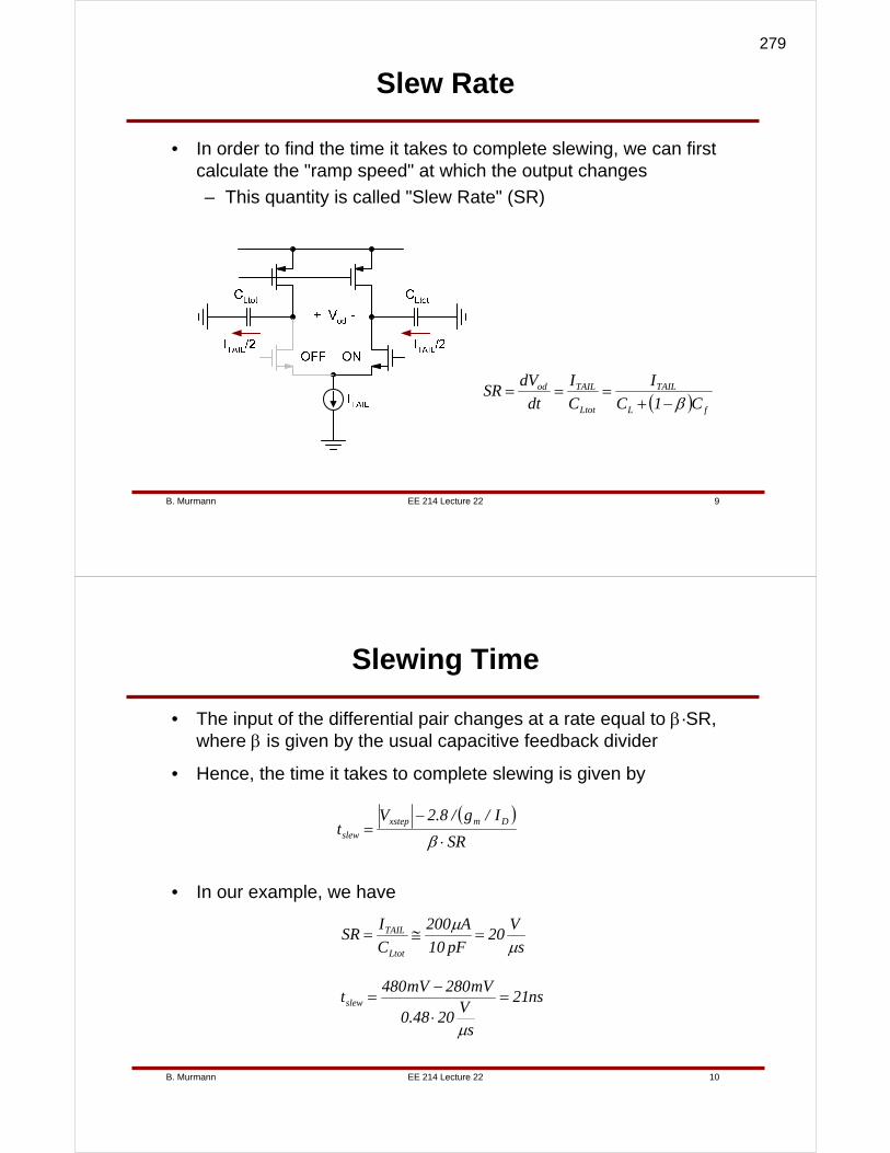
EE 214 Lecture 22B. Murmann 9
Slew Rate
• In order to find the time it takes to complete slewing, we can first calculate the "ramp speed" at which the output changes
– This quantity is called "Slew Rate" (SR)
( ) fL
TAIL
Ltot
TAILod
C1C
I
C
I
dt
dVSR
β−+===
EE 214 Lecture 22B. Murmann 10
Slewing Time
• The input of the differential pair changes at a rate equal to β·SR, where β is given by the usual capacitive feedback divider
• Hence, the time it takes to complete slewing is given by
( )SR
I/g/8.2Vt
Dmxstep
slew ⋅
−=
β
• In our example, we have
s
V20
pF10
A200
C
ISR
Ltot
TAIL
μμ
=≅=
ns21
sV
2048.0
mV280mV480tslew =
⋅
−=
μ
279
EE 214 Lecture 22B. Murmann 11
Subsequent Linear Settling
• Once slewing is completed, the differential output voltage is
mV420SRtV slewslew,od =⋅=
• The final settling value in our example is roughly 1V
– Almost half way there after slewing
• This means that the dynamic error budget for the remaining settling portion has increased
– E.g. if we wanted to settle within 0.1% of the final value (~1V), we only need to complete the remaining transient to within 0.1%·1V/0.58V=0.17%
– Not a very big win, usually a negligible change in the number of required time constants
• 0.1%→6.9τ, 0.17% → 6.4τ
EE 214 Lecture 22B. Murmann 12
Complete Expression for Settling Time
• Note that circuits with large closed loop gain tend to slew less
– Since Vidstep cannot be larger than Voutputswing/Gain
– E.g. Voutputswing=2V, Gain =8 ⇒ Vxdstep < Vidstep < 250mV• Won’t slew at all if gm/ID < 2.8/250mV= 11.2V-1
( ) ( )tol,d
Dmxstep
linslews lnSR
I/g/8.2Vttt ετ
β−
⋅
−≅+=
( ) fL
TAIL
Ltot
TAIL
C1C
I
C
ISR
β−+==
fins
sidstep
Lf
Lfins
sidstepxdstep CCC
CV
CC
CCCC
CVV
++≅
+++
=
insf
f
CCC
C
++=β
<1
280
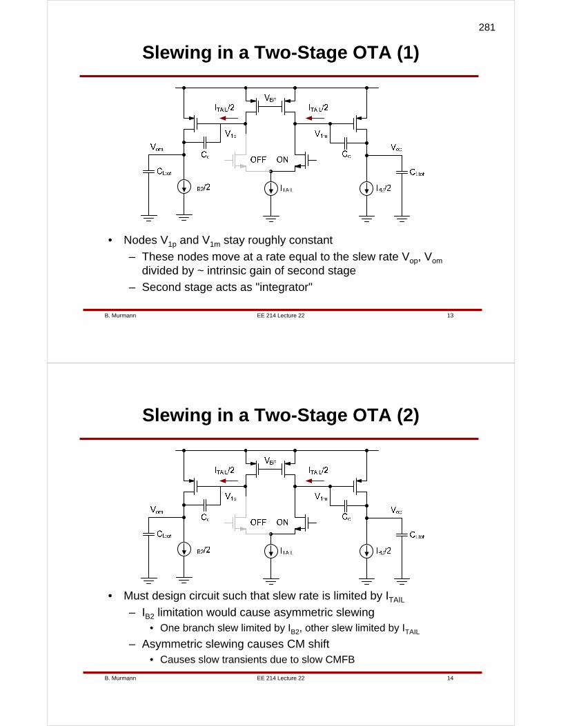
EE 214 Lecture 22B. Murmann 13
Slewing in a Two-Stage OTA (1)
• Nodes V1p and V1m stay roughly constant
– These nodes move at a rate equal to the slew rate Vop, Vom
divided by ~ intrinsic gain of second stage
– Second stage acts as "integrator"
EE 214 Lecture 22B. Murmann 14
Slewing in a Two-Stage OTA (2)
• Must design circuit such that slew rate is limited by ITAIL
– IB2 limitation would cause asymmetric slewing• One branch slew limited by IB2, other slew limited by ITAIL
– Asymmetric slewing causes CM shift• Causes slow transients due to slow CMFB
281
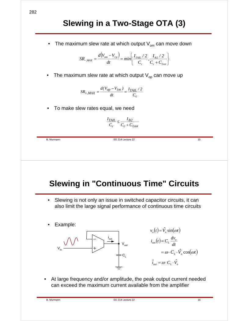
EE 214 Lecture 22B. Murmann 15
Slewing in a Two-Stage OTA (3)
• The maximum slew rate at which output Vom can move down
( )⎭⎬⎫
⎩⎨⎧
+=
−=−
Ltotc
2B
c
TAILp1omMAX, CC
2/I,
C
2/Imin
dt
VVdSR
• The maximum slew rate at which output Vop can move up
c
TAILm1opMAX, C
2/I
dt
)VV(dSR =
−=+
• To make slew rates equal, we need
Ltotc
2B
c
TAIL
CC
I
C
I
+≤
EE 214 Lecture 22B. Murmann 16
Slewing in "Continuous Time" Circuits
• Slewing is not only an issue in switched capacitor circuits, it can also limit the large signal performance of continuous time circuits
• Example:
CL
iout
VoutVin
( ) ( )tVtv oo ωsinˆ=
( )dt
dvCti o
Lout =
oLout VCi ⋅⋅= ω
• At large frequency and/or amplitude, the peak output current needed can exceed the maximum current available from the amplifier
( )tVC oL ωω cosˆ⋅⋅=
282
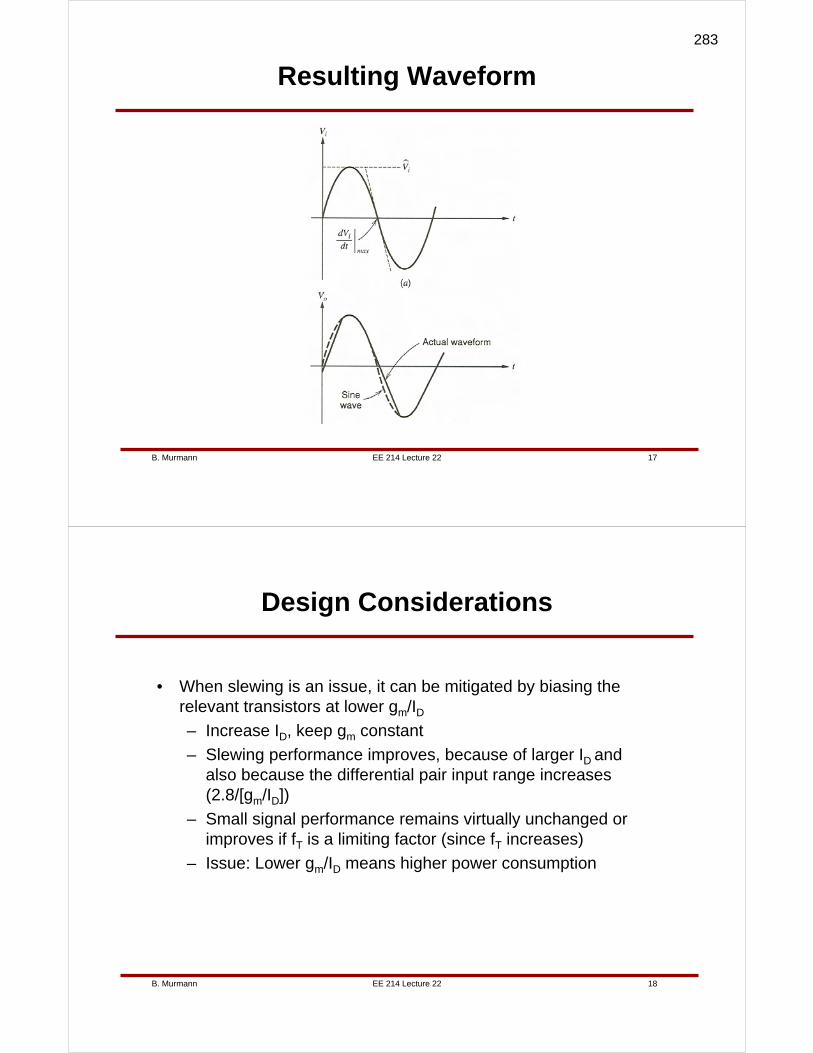
EE 214 Lecture 22B. Murmann 17
Resulting Waveform
EE 214 Lecture 22B. Murmann 18
Design Considerations
• When slewing is an issue, it can be mitigated by biasing the relevant transistors at lower gm/ID– Increase ID, keep gm constant
– Slewing performance improves, because of larger ID and also because the differential pair input range increases (2.8/[gm/ID])
– Small signal performance remains virtually unchanged or improves if fT is a limiting factor (since fT increases)
– Issue: Lower gm/ID means higher power consumption
283

EE 214 Lecture 22B. Murmann 19
How to Incorporate Slewing in Design Flow
• Set up a spreadsheet for small signal design as usual– Settling time requirement translates into minimum "linear"
bandwidth spec (based on linear analysis, without slewing)
• Introduce a bandwidth spec scale factor K≥1 in your design script– If the circuit slews, we will need more bandwidth than
predicted from linear analysis
• Perform design optimization as usual, begin with K=1
• Calculate slewing time, add to linear settling time– Done if tslew=0
• Increase K until design meets settling time spec– In the process, you may consider to optimize gm/ID values to
minimize power in presence of slewing
284
EE 214 Lecture 23B. Murmann 1
Lecture 23Feedback and Port Impedances
OTA Variants, CMFB Implementation
Boris MurmannStanford University
Copyright © 2007 by Boris Murmann
EE 214 Lecture 23B. Murmann 2
Overview
• Reading– 8.8.2 (Closed-Loop Impedance Formula using Return Ratio)– 6.7 (MOS Active-Cascode Amplifiers)– 12.5 (CMFB Circuits)– 12.6 (Fully Differential Amplifiers)– 9.4.4 (Compensation of Single Stage CMOS OTAs)
• Reference– K. Bult, G.J.G.M. Geelen, "A fast-settling CMOS op-amp for SC circuits with
90-dB DC gain," IEEE J. Solid-State Circuits, Dec. 1990, pp. 1379 – 1384.
• Introduction– In order to complete our framework for feedback circuit analysis, we will
study the effect of feedback on port impedances in today's lecture. A useful analytical tool for quick calculations is Blackman's Impedance Formula, which allows us to find port impedances based on a superposition of simple sub-analyses.
– Next, we survey common OTA architectures and associated implementation aspects. Most OTAs used in practice are derivatives of the basic single- or two-stage topology, with add-ons such as simple cascodes or gain boosted cascodes. The survey concludes with a brief analysis of the most commonly used common mode feedback implementations.
285
EE 214 Lecture 23B. Murmann 3
Using Feedback to Modify Port Impedances
• Our initial motivation for using feedback was to build precise gain elements that are insensitive to gmR variations
• In addition, feedback can be used to increase/decrease port impedances
– In fact, we have already seen one example of such behavior• Closed loop bandwidth of OTA feedback amplifier was (1+T)
higher than open loop bandwidth
• This means the impedance seen by the load capacitor must have dropped in presence of feedback
• We can calculate the port impedances of arbitrary feedback circuits using "Blackman's Impedance Formula"
– Based on loop gain calculations
– Extremely useful and easy to use
EE 214 Lecture 23B. Murmann 4
Blackman's Impedance Formula
1. First, find port impedance with feedback loop broken
– E.g. set gm=0
2. Calculate loop gain in circuit with port under consideration shorted
3. Calculate loop gain in circuit with port under consideration open
• In many cases, either the "shorted" or "open" loop gain is zero
( ) ( )( )open portT
shortedportTkZZ portport +
+⋅==
1
10
286
EE 214 Lecture 23B. Murmann 5
Example 1
( ) ( )m
voutout gaRkR
100 ====
( ) 0= shortedportT
( ) vaopen portT =
vmout ag
R+
=1
11
EE 214 Lecture 23B. Murmann 6
Example 2: Shunt-Shunt Stage
( ) oFmin rRgR +== 0
( ) 0= shortedinputT
( ) omrgopen inputT =
( ) ⎟⎟⎠
⎞⎜⎜⎝
⎛+≅
++=
o
F
momoFin r
R
grgrRR 1
1
1
1
( ) omout rgR == 0
( ) 0= shortedoutputT
( ) omrgopen outputT =
momoout grg
rR1
1
1≅
+=
287
EE 214 Lecture 23B. Murmann 7
Example 3: Active Cascode
• Also referred to as "Regulated Cascode" or "Gain Boosting" technique
( ) 22010 omvout rgraR ⋅≅=
( ) vmbm
mv a
gg
ga shortedportT ≅
+≅
22
2
( ) 0=open portT
( )vom
vomout
argr
argrR
⋅⋅≅+⋅⋅≅
2201
2201 1
EE 214 Lecture 23B. Murmann 8
Basic Implementation
• Can use simple CS stage as auxiliary amplifier
– Issue: Costs headroom
• See literature for more advanced implementations
– E.g. using fully differential folded cascode amplifier as an auxiliary amplifier
332201 omomout rgrgrR ⋅⋅≅
288
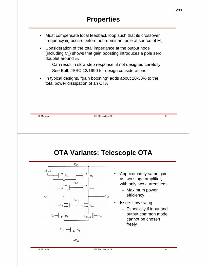
EE 214 Lecture 23B. Murmann 9
Properties
• Must compensate local feedback loop such that its crossover frequency ωc occurs before non-dominant pole at source of M2.
• Consideration of the total impedance at the output node (including CL) shows that gain boosting introduces a pole zero doublet around ωc
– Can result in slow step response, if not designed carefully
– See Bult, JSSC 12/1990 for design considerations
• In typical designs, "gain boosting" adds about 20-30% to the total power dissipation of an OTA
EE 214 Lecture 23B. Murmann 10
OTA Variants: Telescopic OTA
• Approximately same gain as two stage amplifier, with only two current legs
– Maximum power efficiency
• Issue: Low swing
– Especially if input and output common mode cannot be chosen freely
289
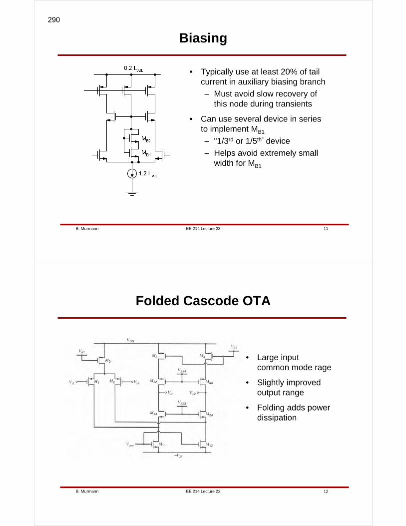
EE 214 Lecture 23B. Murmann 11
Biasing
• Typically use at least 20% of tail current in auxiliary biasing branch
– Must avoid slow recovery of this node during transients
• Can use several device in series to implement MB1
– "1/3rd or 1/5th" device
– Helps avoid extremely small width for MB1
EE 214 Lecture 23B. Murmann 12
Folded Cascode OTA
• Large input common mode rage
• Slightly improved output range
• Folding adds power dissipation
290
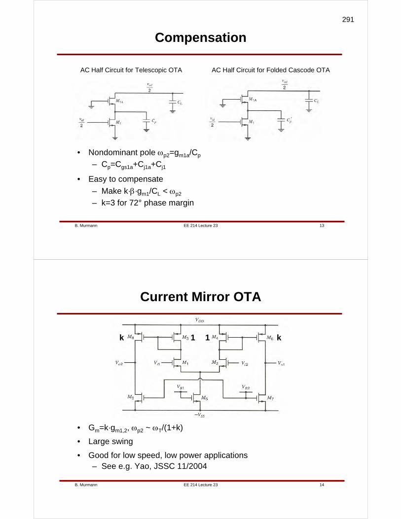
EE 214 Lecture 23B. Murmann 13
Compensation
• Nondominant pole ωp2=gm1a/Cp
– Cp=Cgs1a+Cj1a+Cj1
• Easy to compensate
– Make k·β·gm1/CL < ωp2
– k=3 for 72° phase margin
AC Half Circuit for Telescopic OTA AC Half Circuit for Folded Cascode OTA
EE 214 Lecture 23B. Murmann 14
Current Mirror OTA
• Gm=k·gm1,2, ωp2 ~ ωT/(1+k)
• Large swing
• Good for low speed, low power applications– See e.g. Yao, JSSC 11/2004
k 1 1 k
291
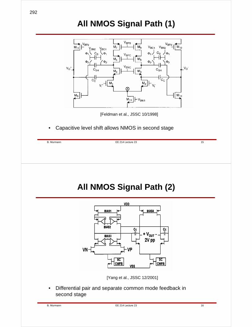
EE 214 Lecture 23B. Murmann 15
All NMOS Signal Path (1)
• Capacitive level shift allows NMOS in second stage
[Feldman et al., JSSC 10/1998]
EE 214 Lecture 23B. Murmann 16
All NMOS Signal Path (2)
• Differential pair and separate common mode feedback in second stage
[Yang et al., JSSC 12/2001]
292
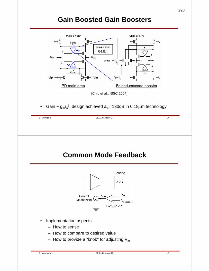
EE 214 Lecture 23B. Murmann 17
Gain Boosted Gain Boosters
• Gain ~ gmro6, design achieved av0=130dB in 0.18μm technology
[Chiu et al., ISSC 2004]
EE 214 Lecture 23B. Murmann 18
Common Mode Feedback
• Implementation aspects
– How to sense
– How to compare to desired value
– How to provide a "knob" for adjusting Voc
293
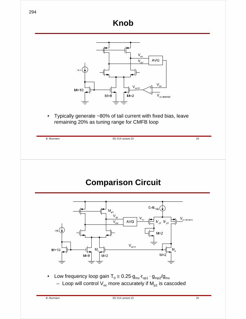
EE 214 Lecture 23B. Murmann 19
Knob
• Typically generate ~80% of tail current with fixed bias, leave remaining 20% as tuning range for CMFB loop
EE 214 Lecture 23B. Murmann 20
Comparison Circuit
• Low frequency loop gain T0 ≅ 0.25·gmx·rop1 · gmp2/gmx
– Loop will control Voc more accurately if Mp1 is cascoded
294
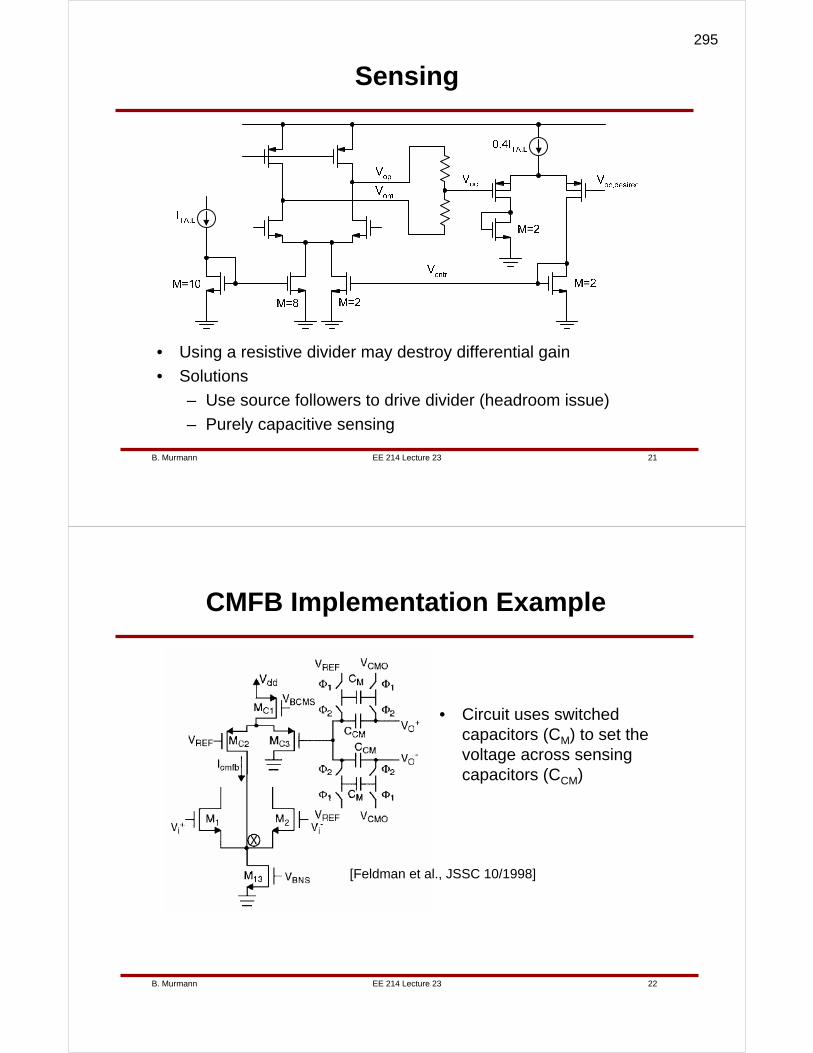
EE 214 Lecture 23B. Murmann 21
Sensing
• Using a resistive divider may destroy differential gain
• Solutions
– Use source followers to drive divider (headroom issue)
– Purely capacitive sensing
EE 214 Lecture 23B. Murmann 22
CMFB Implementation Example
[Feldman et al., JSSC 10/1998]
• Circuit uses switched capacitors (CM) to set the voltage across sensing capacitors (CCM)
295
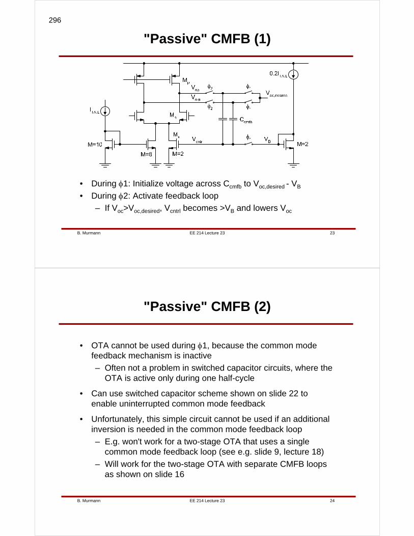
EE 214 Lecture 23B. Murmann 23
"Passive" CMFB (1)
• During φ1: Initialize voltage across Ccmfb to Voc,desired - VB
• During φ2: Activate feedback loop
– If Voc>Voc,desired, Vcntrl becomes >VB and lowers Voc
EE 214 Lecture 23B. Murmann 24
"Passive" CMFB (2)
• OTA cannot be used during φ1, because the common mode feedback mechanism is inactive
– Often not a problem in switched capacitor circuits, where the OTA is active only during one half-cycle
• Can use switched capacitor scheme shown on slide 22 to enable uninterrupted common mode feedback
• Unfortunately, this simple circuit cannot be used if an additional inversion is needed in the common mode feedback loop
– E.g. won't work for a two-stage OTA that uses a single common mode feedback loop (see e.g. slide 9, lecture 18)
– Will work for the two-stage OTA with separate CMFB loops as shown on slide 16
296
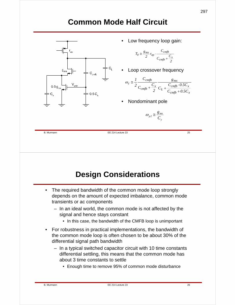
EE 214 Lecture 23B. Murmann 25
Common Mode Half Circuit
• Low frequency loop gain:
2
CC
Cr
2
gT
xcmfb
cmfbop
mx0
+⋅≅
• Loop crossover frequency
xcmfb
xcmfbL
mx
xcmfb
cmfbc
C5.0C
C5.0CC
g
2
CC
C
2
1
+
⋅++
≅ω
• Nondominant pole
y
mn2p C
g≅ω
EE 214 Lecture 23B. Murmann 26
Design Considerations
• The required bandwidth of the common mode loop strongly depends on the amount of expected imbalance, common mode transients or ac components
– In an ideal world, the common mode is not affected by the signal and hence stays constant
• In this case, the bandwidth of the CMFB loop is unimportant
• For robustness in practical implementations, the bandwidth of the common mode loop is often chosen to be about 30% of the differential signal path bandwidth
– In a typical switched capacitor circuit with 10 time constants differential settling, this means that the common mode has about 3 time constants to settle
• Enough time to remove 95% of common mode disturbance
297
EE 214 Lecture 24B. Murmann 1
Lecture 24OTAs with Single Ended Outputs
Output Stage Examples
Boris MurmannStanford University
Copyright © 2007 by Boris Murmann
EE 214 Lecture 24B. Murmann 2
Overview
• Reading
– 4.3.5 (Differential Pair with Current Mirror Load)
– 6.3.3 (Systematic Offset in Two-Stage Amplifier)
– Chapter 5 (Output Stages)
• Introduction
– This lecture concludes our discussion of amplifier implementations by looking at a number of missing bits and pieces. First, we will discuss subtleties of OTA implementations that use a single ended output. While rarely used in the signal path of high performanceintegrated circuits, OTAs with single ended outputs can be useful as auxiliary amplifiers in biasing circuits. Finally, we will take a brief look at output stages that are suitable for driving resistive loads. While most on-chip loads tend to be capacitive in nature, low impedance drivers are often needed when interfacing to off-chip components and wire lines.
298
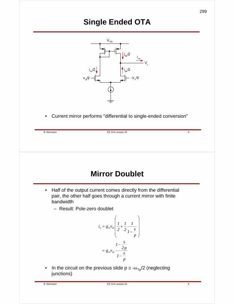
EE 214 Lecture 24B. Murmann 3
Single Ended OTA
• Current mirror performs "differential to single-ended conversion"
EE 214 Lecture 24B. Murmann 4
Mirror Doublet
• Half of the output current comes directly from the differential pair, the other half goes through a current mirror with finite bandwidth
– Result: Pole-zero doublet
ps
1
p2s
1vg
ps
1
1
2
1
2
1vgi
idm
idmo
−
−=
⎟⎟⎟⎟
⎠
⎞
⎜⎜⎜⎜
⎝
⎛
−+=
• In the circuit on the previous slide p ≅ -ωTp/2 (neglecting junctions)
299
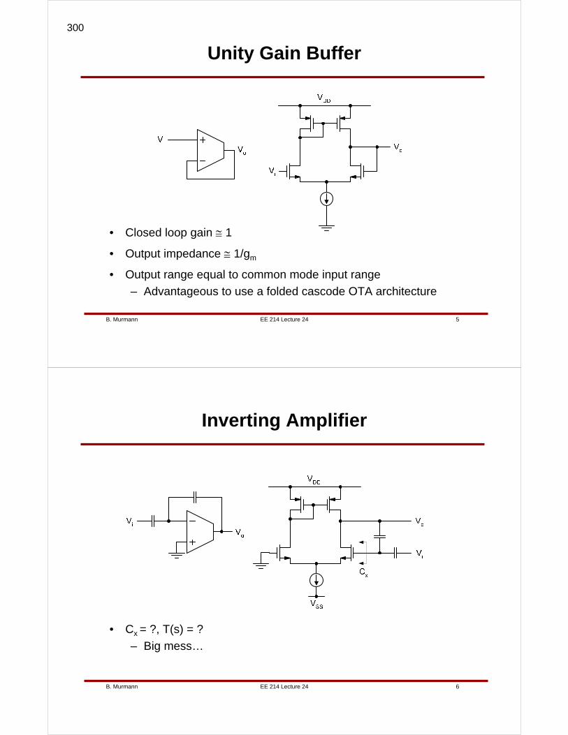
EE 214 Lecture 24B. Murmann 5
Unity Gain Buffer
• Closed loop gain ≅ 1
• Output impedance ≅ 1/gm
• Output range equal to common mode input range
– Advantageous to use a folded cascode OTA architecture
EE 214 Lecture 24B. Murmann 6
Inverting Amplifier
• Cx = ?, T(s) = ?
– Big mess…
300
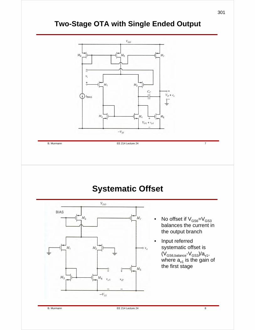
EE 214 Lecture 24B. Murmann 7
Two-Stage OTA with Single Ended Output
EE 214 Lecture 24B. Murmann 8
Systematic Offset
• No offset if VGS6=VGS3
balances the current in the output branch
• Input referred systematic offset is (VGS6,balance-VGS3)/av1, where av1 is the gain of the first stage
301
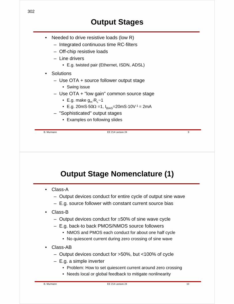
EE 214 Lecture 24B. Murmann 9
Output Stages
• Needed to drive resistive loads (low R)
– Integrated continuous time RC-filters
– Off-chip resistive loads
– Line drivers• E.g. twisted pair (Ethernet, ISDN, ADSL)
• Solutions
– Use OTA + source follower output stage• Swing issue
– Use OTA + "low gain" common source stage• E.g. make gm·RL~1
• E.g. 20mS·50Ω =1, IBIAS=20mS·10V-1 = 2mA
– "Sophisticated" output stages• Examples on following slides
EE 214 Lecture 24B. Murmann 10
Output Stage Nomenclature (1)
• Class-A
– Output devices conduct for entire cycle of output sine wave
– E.g. source follower with constant current source bias
• Class-B
– Output devices conduct for ≅50% of sine wave cycle
– E.g. back-to back PMOS/NMOS source followers• NMOS and PMOS each conduct for about one half cycle
• No quiescent current during zero crossing of sine wave
• Class-AB
– Output devices conduct for >50%, but <100% of cycle
– E.g. a simple inverter• Problem: How to set quiescent current around zero crossing
• Needs local or global feedback to mitigate nonlinearity
302
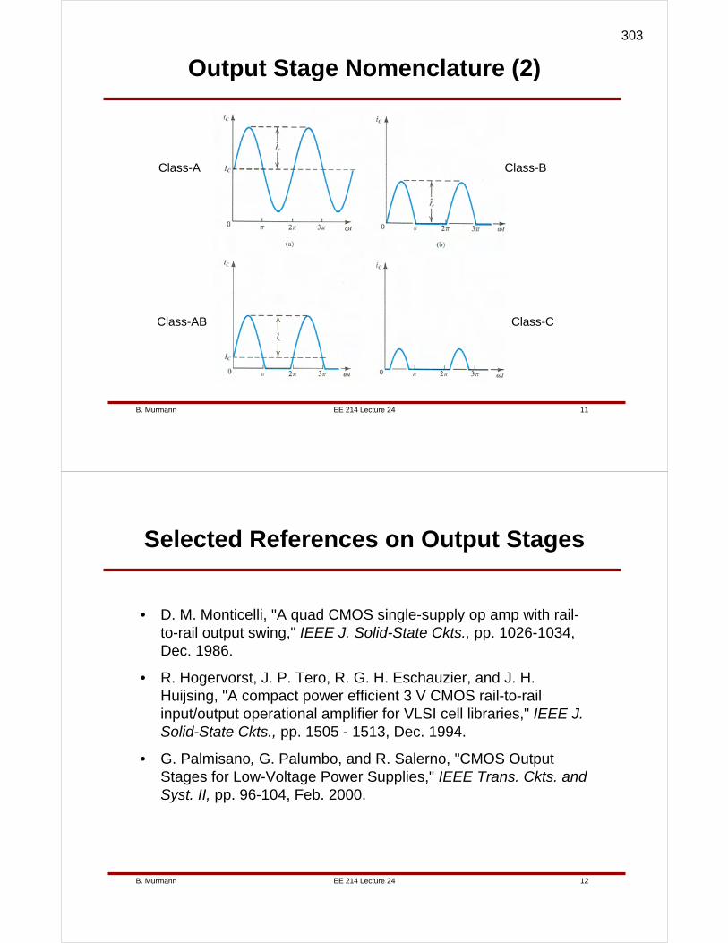
EE 214 Lecture 24B. Murmann 11
Output Stage Nomenclature (2)
Class-A Class-B
Class-AB Class-C
EE 214 Lecture 24B. Murmann 12
Selected References on Output Stages
• D. M. Monticelli, "A quad CMOS single-supply op amp with rail-to-rail output swing," IEEE J. Solid-State Ckts., pp. 1026-1034, Dec. 1986.
• R. Hogervorst, J. P. Tero, R. G. H. Eschauzier, and J. H. Huijsing, "A compact power efficient 3 V CMOS rail-to-rail input/output operational amplifier for VLSI cell libraries," IEEE J. Solid-State Ckts., pp. 1505 - 1513, Dec. 1994.
• G. Palmisano, G. Palumbo, and R. Salerno, "CMOS Output Stages for Low-Voltage Power Supplies," IEEE Trans. Ckts. and Syst. II, pp. 96-104, Feb. 2000.
303
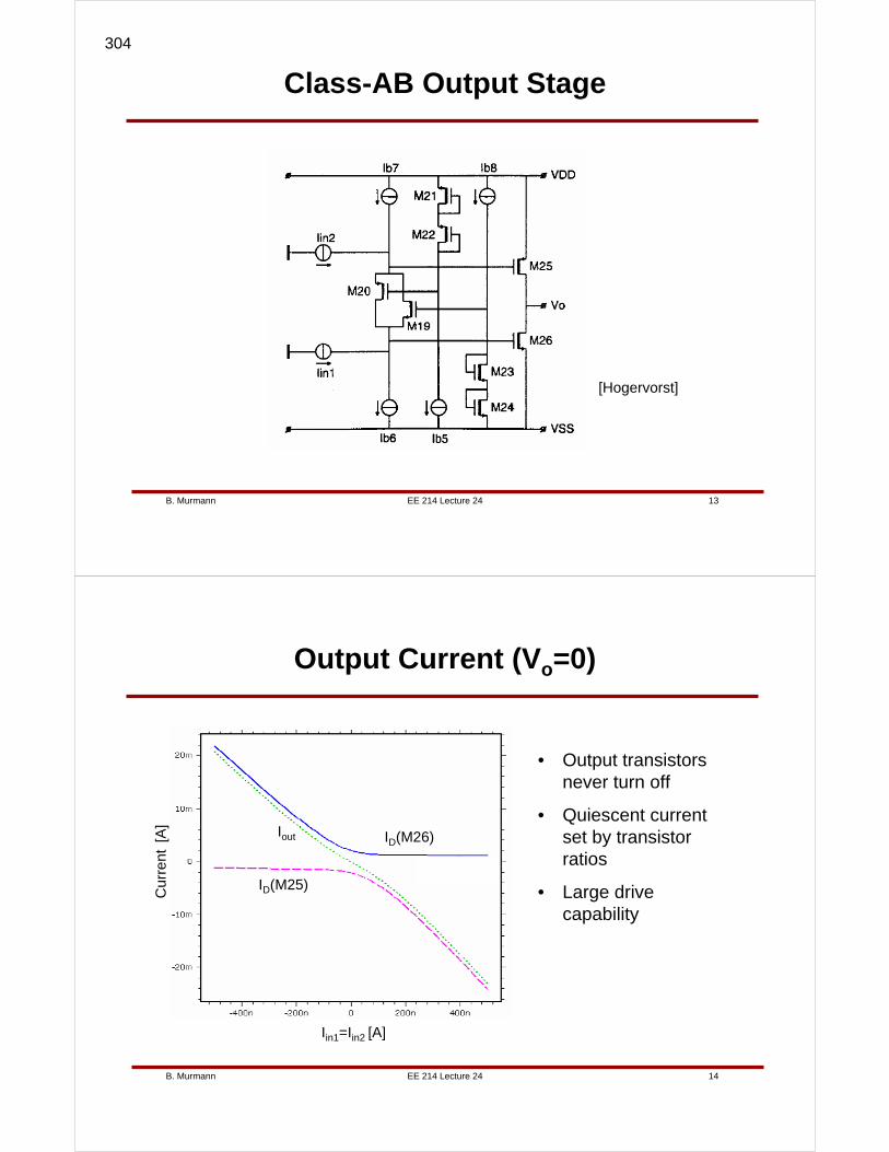
EE 214 Lecture 24B. Murmann 13
Class-AB Output Stage
[Hogervorst]
EE 214 Lecture 24B. Murmann 14
Output Current (Vo=0)
• Output transistors never turn off
• Quiescent current set by transistor ratios
• Large drive capability
ID(M25)
ID(M26)Iout
Iin1=Iin2 [A]
Cur
rent
[A
]
304
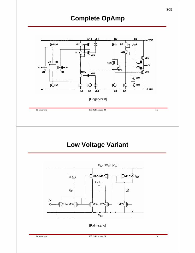
EE 214 Lecture 24B. Murmann 15
Complete OpAmp
[Hogervorst]
EE 214 Lecture 24B. Murmann 16
Low Voltage Variant
[Palmisano]
<Vtn+|Vtp|
305
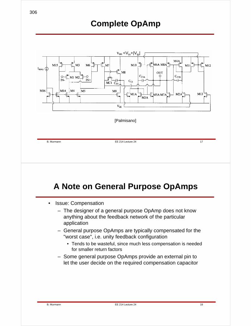
EE 214 Lecture 24B. Murmann 17
Complete OpAmp
[Palmisano]
<Vtn+|Vtp|
EE 214 Lecture 24B. Murmann 18
A Note on General Purpose OpAmps
• Issue: Compensation
– The designer of a general purpose OpAmp does not know anything about the feedback network of the particular application
– General purpose OpAmps are typically compensated for the "worst case", i.e. unity feedback configuration
• Tends to be wasteful, since much less compensation is needed for smaller return factors
– Some general purpose OpAmps provide an external pin to let the user decide on the required compensation capacitor
306

EE 214 Lecture 25B. Murmann 1
Lecture 25Supply Insensitive Biasing
Boris MurmannStanford University
Copyright © 2007 by Boris Murmann
EE 214 Lecture 25B. Murmann 2
Overview
• Reading
– 4.4.2 (Supply Insensitive Biasing)
• Introduction
– Throughout this course, we have ignored the question on how to generate the reference bias currents used in most of our circuits. Today, we will examine a variety of current reference implementations, with primary focus on supply independence.
307
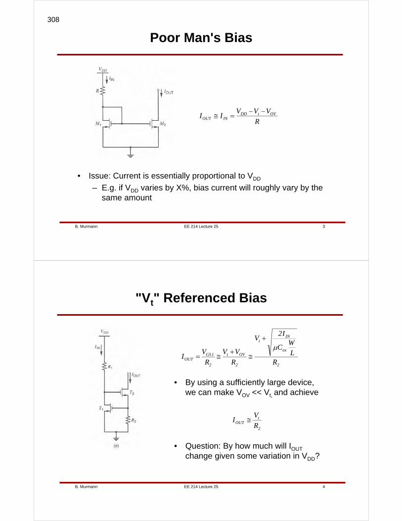
EE 214 Lecture 25B. Murmann 3
Poor Man's Bias
• Issue: Current is essentially proportional to VDD
– E.g. if VDD varies by X%, bias current will roughly vary by the same amount
R
VVVII OVtDD
INOUT
−−=≅
EE 214 Lecture 25B. Murmann 4
"Vt" Referenced Bias
• By using a sufficiently large device, we can make VOV << Vt, and achieve
2
ox
INt
2
OVt
2
1GSOUT R
LW
C
I2V
R
VV
R
VI
μ+
≅+
≅=
2
tOUT R
VI ≅
• Question: By how much will IOUT
change given some variation in VDD?
308
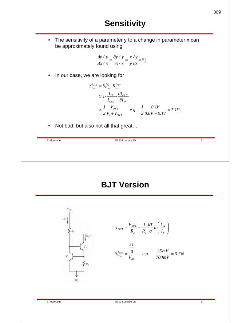
EE 214 Lecture 25B. Murmann 5
Sensitivity
• The sensitivity of a parameter y to a change in parameter x can be approximately found using
yx
!
Sx
y
y
x
x/x
y/y
x/x
y/y=
∂∂
=∂∂
≅ΔΔ
• In our case, we are looking for
%1.7V1.0V6.0
V1.0
2
1.g.e
VV
V
2
1
I
I
I
I1
SSS
1OVt
1OV
IN
OUT
OUT
IN
II
IV
IV
OUT
IN
IN
DD
OUT
DD
=++
≅
∂∂⋅⋅≅
⋅=
• Not bad, but also not all that great…
EE 214 Lecture 25B. Murmann 6
BJT Version
⎟⎟⎠
⎞⎜⎜⎝
⎛==
S
IN
22
1BEOUT I
Iln
q
kT
R
1
R
VI
%7.3mV700
mV26.g.e
Vq
kT
SBE
IV
OUT
DD==
309
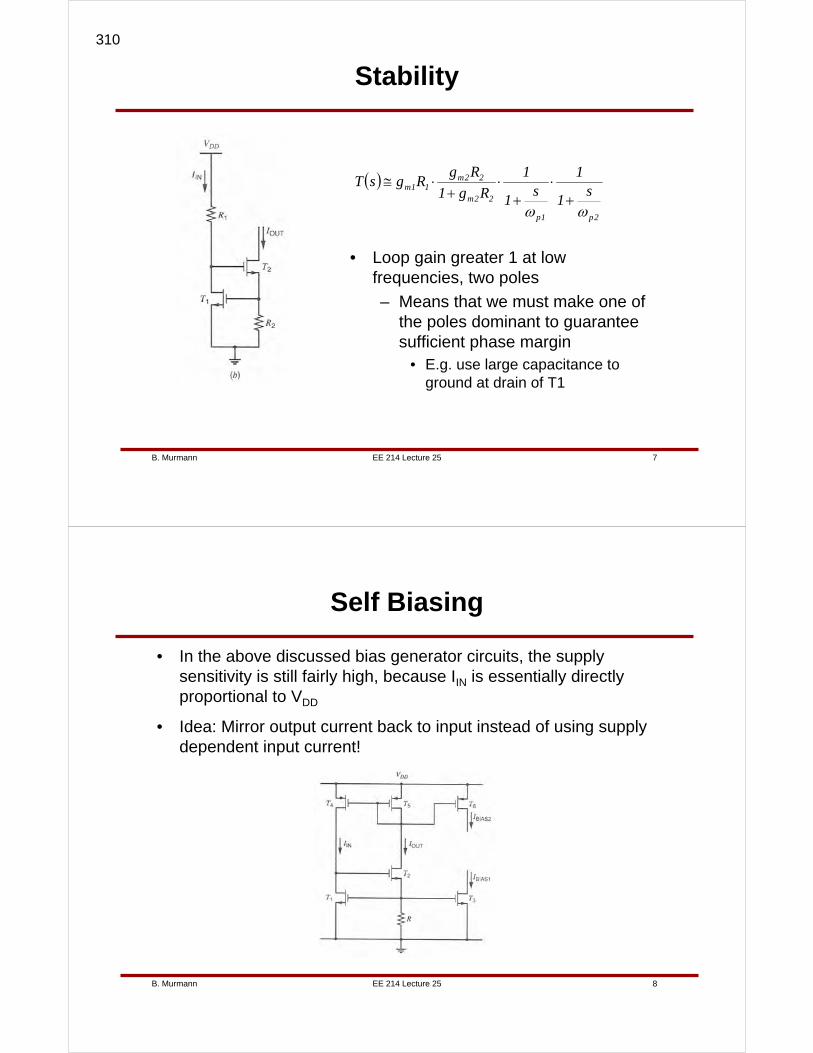
EE 214 Lecture 25B. Murmann 7
Stability
( )
2p1p
22m
22m11m s
1
1s
1
1
Rg1
RgRgsT
ωω+
⋅+
⋅+
⋅≅
• Loop gain greater 1 at low frequencies, two poles
– Means that we must make one of the poles dominant to guarantee sufficient phase margin
• E.g. use large capacitance to ground at drain of T1
EE 214 Lecture 25B. Murmann 8
Self Biasing
• In the above discussed bias generator circuits, the supply sensitivity is still fairly high, because IIN is essentially directly proportional to VDD
• Idea: Mirror output current back to input instead of using supply dependent input current!
310
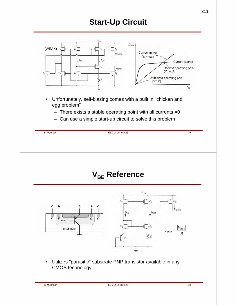
EE 214 Lecture 25B. Murmann 9
Start-Up Circuit
• Unfortunately, self-biasing comes with a built in "chicken and egg problem"
– There exists a stable operating point with all currents =0
– Can use a simple start-up circuit to solve this problem
(WEAK)
EE 214 Lecture 25B. Murmann 10
VBE Reference
• Utilizes "parasitic" substrate PNP transistor available in any CMOS technology
R
VI 1BE
OUT =
311
EE 214 Lecture 25B. Murmann 11
Temperature Dependence (1)
• Similar to the sensitivity to supply variations, we can establish an expression for temperature variations
– Fractional temperature coefficient
OUT
OUT
F IT
I
TC ∂∂
=
• For the circuit on the previous slide we have
R
VI 1BE
OUT =
⎟⎟⎠
⎞⎜⎜⎝
⎛∂∂
−∂∂
=
∂∂
−∂∂
=∂∂
T
R
R
1
T
V
V
1I
T
R
R
V
T
V
R
1
T
I
1BE
1BEOUT
21BE1BEOUT
EE 214 Lecture 25B. Murmann 12
Temperature Dependence (2)
• Final result
• Temperature dependence is usually quite high
T
R
R
1
T
V
V
1TC 1BE
1BEF ∂
∂−
∂∂
=
K/%33.0mV600
K/mV2
T
V
V
1 1BE
1BE
−=−
≅∂∂
resistor)(poly K/%2.0T
R
R
1+≅
∂∂
• E.g. ΔT=100K ⇒ ΔI=-53% (!)
K/%53.0TCF −=
312
EE 214 Lecture 25B. Murmann 13
ΔVBE Reference
( )nlnq
kT
I
I
I
Iln
q
kT
I
Iln
q
kT
I
Iln
q
kT
VVRI
IN
2S
1S
IN
2S
OUT
1S
IN
2BE1BEOUT
=
⎟⎟⎠
⎞⎜⎜⎝
⎛=
⎟⎟⎠
⎞⎜⎜⎝
⎛−⎟⎟⎠
⎞⎜⎜⎝
⎛=
−=⋅
( )nlnq
kT
R
1IOUT =
EE 214 Lecture 25B. Murmann 14
TC of ΔVBE Reference
( )
( ) ⎟⎟⎠
⎞⎜⎜⎝
⎛∂∂
−∂∂
=
∂∂
−∂∂
=∂∂
T
R
R
1
T
V
V
1
R
Vnln
RTR
VTV
Rnln
T
I
T
T2
T
2
TT
OUT
T
R
R
1
T
1
T
R
R
1
T
V
V
1TC T
TF ∂
∂−=
∂∂
−∂∂
=
q
kTVT =
• ExampleK/%13.0K/%2.0
K300
1TCF =−=
• TC of resistor and kT/q partially cancel!
313
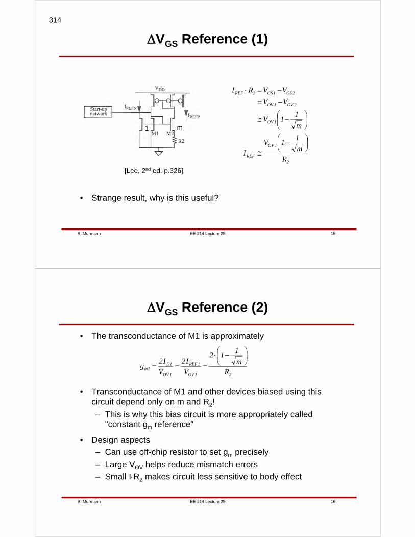
EE 214 Lecture 25B. Murmann 15
ΔVGS Reference (1)
• Strange result, why is this useful?
2
1OV
REF
1OV
2OV1OV
2GS1GS2REF
Rm
11V
I
m
11V
VV
VVRI
⎟⎠⎞
⎜⎝⎛ −
≅
⎟⎠
⎞⎜⎝
⎛ −≅
−=−=⋅
[Lee, 2nd ed. p.326]
m1
EE 214 Lecture 25B. Murmann 16
ΔVGS Reference (2)
• The transconductance of M1 is approximately
21OV
1REF
1OV
1D1m R
m
112
V
I2
V
I2g
⎟⎠
⎞⎜⎝
⎛ −⋅===
• Transconductance of M1 and other devices biased using this circuit depend only on m and R2!
– This is why this bias circuit is more appropriately called "constant gm reference"
• Design aspects
– Can use off-chip resistor to set gm precisely
– Large VOV helps reduce mismatch errors
– Small I⋅R2 makes circuit less sensitive to body effect
314
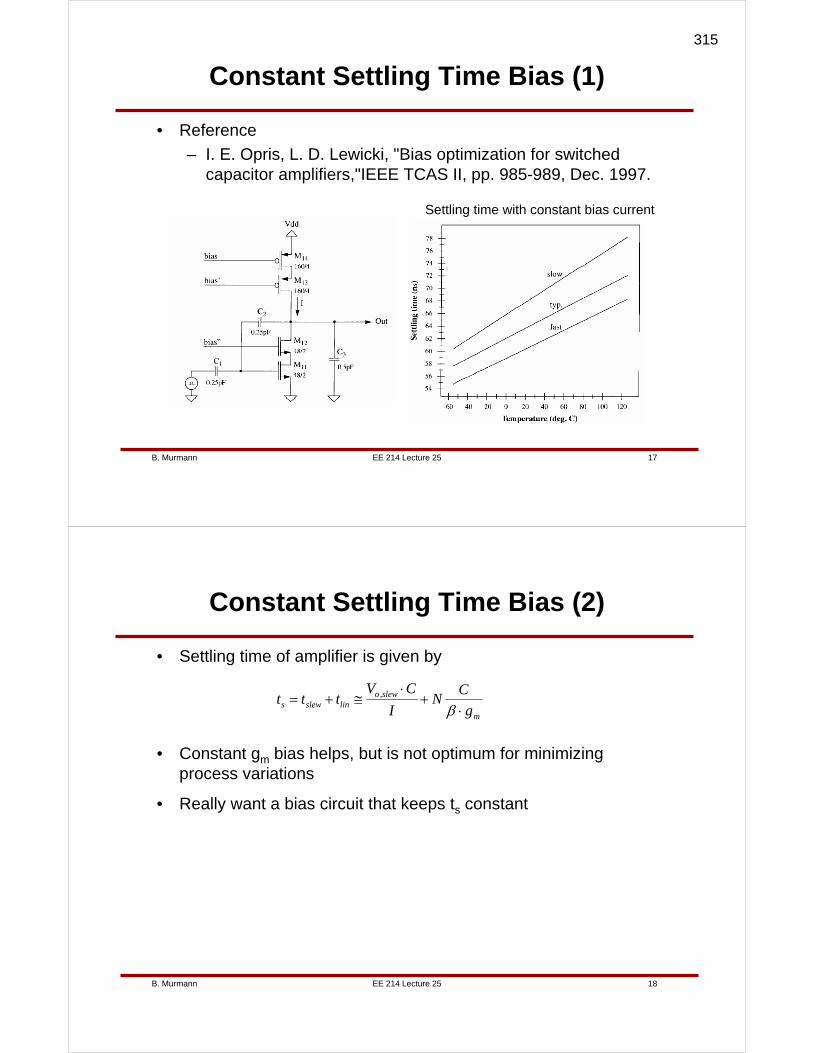
EE 214 Lecture 25B. Murmann 17
Constant Settling Time Bias (1)
• Reference
– I. E. Opris, L. D. Lewicki, "Bias optimization for switched capacitor amplifiers,"IEEE TCAS II, pp. 985-989, Dec. 1997.
Settling time with constant bias current
EE 214 Lecture 25B. Murmann 18
Constant Settling Time Bias (2)
• Settling time of amplifier is given by
m
slew,olinslews g
CN
I
CVttt
⋅+
⋅≅+=
β
• Constant gm bias helps, but is not optimum for minimizing process variations
• Really want a bias circuit that keeps ts constant
315
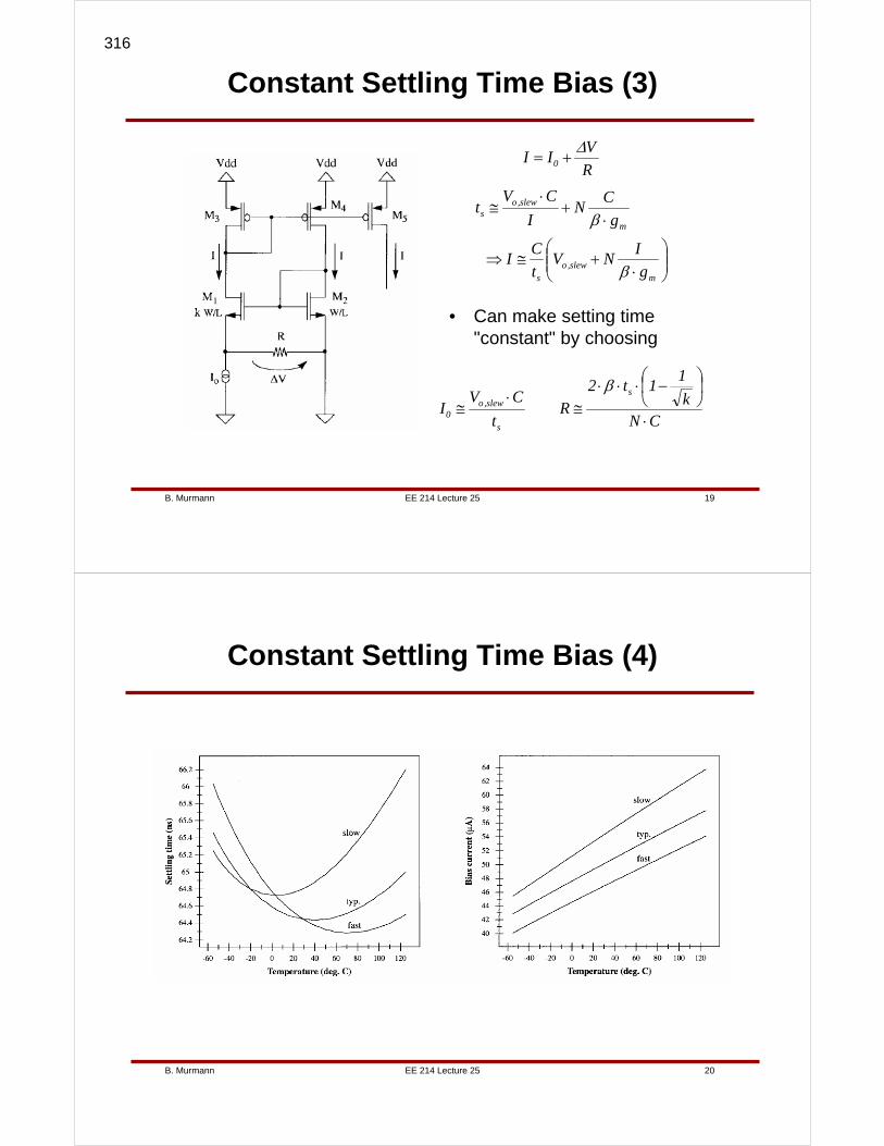
EE 214 Lecture 25B. Murmann 19
Constant Settling Time Bias (3)
• Can make setting time "constant" by choosing
R
VII 0
Δ+=
⎟⎟⎠
⎞⎜⎜⎝
⎛⋅
+≅⇒
⋅+
⋅≅
mslew,o
s
m
slew,os
g
INV
t
CI
g
CN
I
CVt
β
β
CNk
11t2
Rt
CVI
s
s
slew,o0 ⋅
⎟⎠⎞
⎜⎝⎛ −⋅⋅⋅
≅⋅
≅β
EE 214 Lecture 25B. Murmann 20
Constant Settling Time Bias (4)
316

EE 214 Lecture 26B. Murmann 1
Lecture 26Bandgap Reference
Boris MurmannStanford University
Copyright © 2007 by Boris Murmann
EE 214 Lecture 26B. Murmann 2
Overview
• Reading
– 4.4.3 (Temperature Insensitive Biasing)
• Introduction
– In this lecture we will introduce the basic idea behind the frequently used "bandgap" voltage reference. Conceptually, a bandgap reference simply combines two quantities with opposite temperature behavior to generate a voltage with (approximately) zero TC.
317
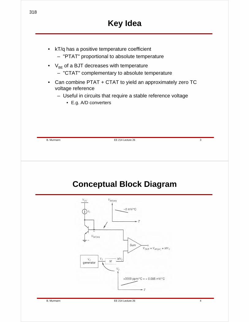
EE 214 Lecture 26B. Murmann 3
Key Idea
• kT/q has a positive temperature coefficient
– "PTAT" proportional to absolute temperature
• VBE of a BJT decreases with temperature
– "CTAT" complementary to absolute temperature
• Can combine PTAT + CTAT to yield an approximately zero TC voltage reference
– Useful in circuits that require a stable reference voltage• E.g. A/D converters
EE 214 Lecture 26B. Murmann 4
Conceptual Block Diagram
318
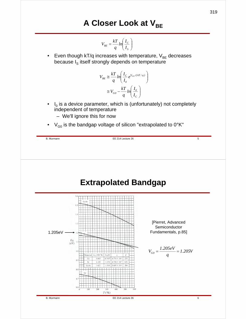
EE 214 Lecture 26B. Murmann 5
A Closer Look at VBE
• Even though kT/q increases with temperature, VBE decreases because IS itself strongly depends on temperature
⎟⎟⎠
⎞⎜⎜⎝
⎛=
S
CBE I
Iln
q
kTV
⎟⎟⎠
⎞⎜⎜⎝
⎛−≅
⎟⎟⎠
⎞⎜⎜⎝
⎛≅
C
00G
)q/kT/(V
0
CBE
I
Iln
q
kTV
eI
Iln
q
kTV 0G
• I0 is a device parameter, which is (unfortunately) not completely independent of temperature– We'll ignore this for now
• VG0 is the bandgap voltage of silicon "extrapolated to 0°K"
EE 214 Lecture 26B. Murmann 6
Extrapolated Bandgap
1.205eV
V205.1q
eV205.1V 0G ==
[Pierret, Advanced Semiconductor
Fundamentals, p.85]
319
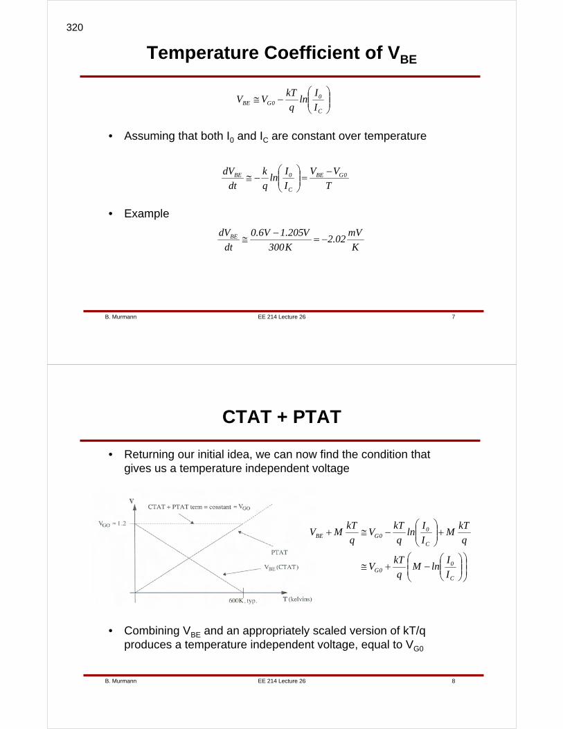
EE 214 Lecture 26B. Murmann 7
Temperature Coefficient of VBE
• Assuming that both I0 and IC are constant over temperature
T
VV
I
Iln
q
k
dt
dV 0GBE
C
0BE −=⎟⎟
⎠
⎞⎜⎜⎝
⎛−≅
• Example
⎟⎟⎠
⎞⎜⎜⎝
⎛−≅
C
00GBE I
Iln
q
kTVV
K
mV02.2
K300
V205.1V6.0
dt
dVBE −=−
≅
EE 214 Lecture 26B. Murmann 8
CTAT + PTAT
• Returning our initial idea, we can now find the condition that gives us a temperature independent voltage
⎟⎟⎠
⎞⎜⎜⎝
⎛⎟⎟⎠
⎞⎜⎜⎝
⎛−+≅
+⎟⎟⎠
⎞⎜⎜⎝
⎛−≅+
C
00G
C
00GBE
I
IlnM
q
kTV
q
kTM
I
Iln
q
kTV
q
kTMV
• Combining VBE and an appropriately scaled version of kT/q produces a temperature independent voltage, equal to VG0
320
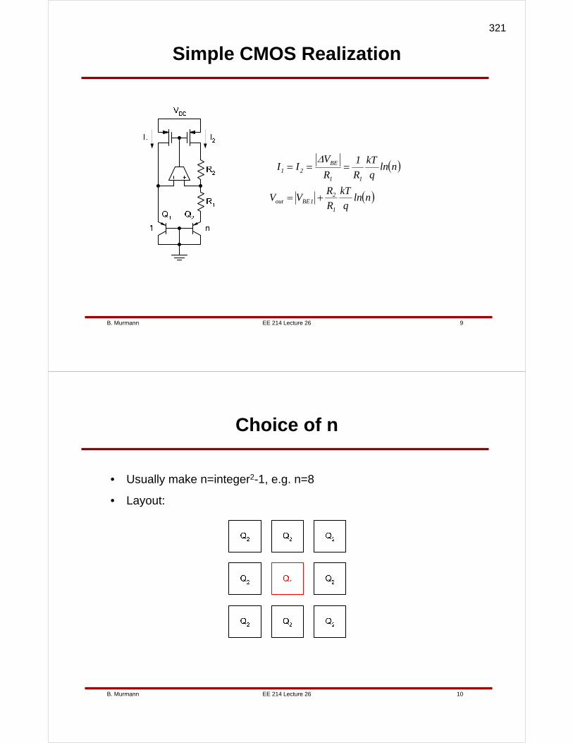
EE 214 Lecture 26B. Murmann 9
Simple CMOS Realization
( )
( )nlnq
kT
R
RVV
nlnq
kT
R
1
R
VII
1
21BEout
11
BE21
+=
===Δ
EE 214 Lecture 26B. Murmann 10
Choice of n
• Usually make n=integer2-1, e.g. n=8
• Layout:
321

EE 214 Lecture 26B. Murmann 11
Design Example
• From measurement data, we know that |VBE| of a unit device is 700mV at room temperature and I=50μA
• Decided to use n=8
( ) ( )
( ) ( ) ΩΩ
Ωμ
k34.98lnmV26
V7.0V205.1k08.1
nlnq
kTVV
RR
k08.18lnmV26A50
1nln
q
kT
I
1R
1BEGO12
21
=−
=−
=
===
EE 214 Lecture 26B. Murmann 12
Nonidealities
• "Curvature"
– Temperature dependence of I0
• Offset voltages and TC of offset voltages
• Resistor mismatch and TC
• Finite β and β mismatch
• More next lecture…
322

EE 214 Lecture 27B. Murmann 1
Lecture 27Bandgap Reference
(Continued)
Boris MurmannStanford University
Copyright © 2007 by Boris Murmann
EE 214 Lecture 27B. Murmann 2
Overview
• Reading
– 4.4.3 (Temperature Insensitive Biasing)
• Introduction
– Today's lecture will cover several important details that we've left out in our previous analysis of bandgap references. We will discuss nonidealities such as "curvature" and the impact of offset voltages. Finally, we will take a brieflook at state-of-the art implementations and performance.
323
EE 214 Lecture 27B. Murmann 3
Selected References (1)
• R. J. Widlar, "New developments in IC voltage regulators," IEEE J. Solid-State Circuits, pp. 2-7, Feb. 1971.– First report, LM309 5V regulator
• A. P. Brokaw, "A simple three-terminal IC bandgap reference,"IEEE J. Solid-State Circuits, pp. 388-393, Dec. 1974.– A classic implementation
• C. Palmer and R. Dobkin, "A curvature corrected micropower voltage reference," IEEE Int. Solid-State Conference, pp. 58-59, Feb. 1981.
• G. Nicollini et al., "A CMOS bandgap reference for differential signal processing," IEEE J. Solid-State Circuits, pp. 41-50, Jan. 1991.– Offset compensated amplifier
EE 214 Lecture 27B. Murmann 4
Selected References (2)
• T.L. Brooks et al., "A low-power differential CMOS bandgap reference," IEEE Int. Solid-State Conf., pp. 248-249, Feb. 1994.– Differential output, stacked diodes
• H. Banda et al. "A CMOS bandgap reference circuit with sub-1-V operation," IEEE J. Solid-State Circuits, pp. 670 - 674, May 1999 .
• P. Malcovati et al., "Curvature-compensated BiCMOS bandgap with 1-V supply voltage," IEEE J. Solid-State Circuits, pp. 1076-1081, July 2001.
324
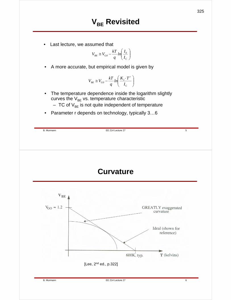
EE 214 Lecture 27B. Murmann 5
VBE Revisited
• Last lecture, we assumed that
⎟⎟⎠
⎞⎜⎜⎝
⎛−≅
C
00GBE I
Iln
q
kTVV
• A more accurate, but empirical model is given by
⎟⎟⎠
⎞⎜⎜⎝
⎛ ⋅−≅
C
r1
0GBE I
TKln
q
kTVV
• The temperature dependence inside the logarithm slightly curves the VBE vs. temperature characteristic– TC of VBE is not quite independent of temperature
• Parameter r depends on technology, typically 3…6
EE 214 Lecture 27B. Murmann 6
Curvature
[Lee, 2nd ed., p.322]
325
EE 214 Lecture 27B. Murmann 7
Collector Current
• Another superficial assumption was to assume that the current IC is independent of temperature
– Actually PTAT in the example circuit from last lecture
– Also affected by TC of resistors
• To capture the temperature behavior of IC, we can introduce yet another empirical fudge factor and write
⎟⎟⎠
⎞⎜⎜⎝
⎛−≅
n
r
0GBE T
TKln
q
kTVV
• The factor n is 1 for ideal PTAT current behavior
EE 214 Lecture 27B. Murmann 8
Modified TC of VBE
• With this refinement, we have
( )
( )
( )
Tq
kTnrVV
nrT
TKln
q
k
TT
K
TnrK
q
kT
T
TKln
q
k
T
TKln
q
kT
dT
d
dT
dV
BE0G
n
r
n
r
1nr
n
r
n
rBE
−+−−=
⎥⎦
⎤⎢⎣
⎡−−⎟⎟
⎠
⎞⎜⎜⎝
⎛−≅
−−⎟⎟
⎠
⎞⎜⎜⎝
⎛−≅
⎥⎦
⎤⎢⎣
⎡⎟⎟⎠
⎞⎜⎜⎝
⎛−≅
−−
326
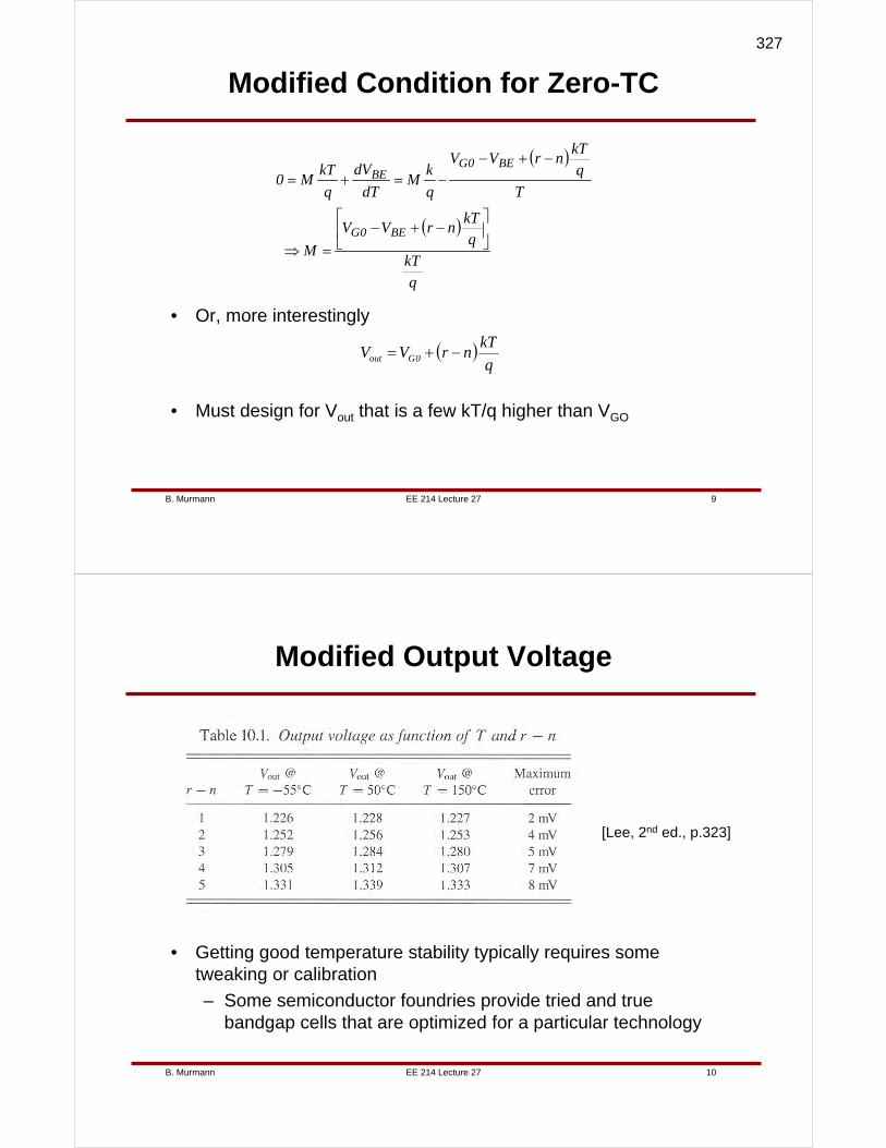
EE 214 Lecture 27B. Murmann 9
Modified Condition for Zero-TC
• Or, more interestingly
( )
( )
q
kT
q
kTnrVV
M
T
q
kTnrVV
q
kM
dT
dV
q
kTM0
BE0G
BE0GBE
⎥⎦
⎤⎢⎣
⎡−+−
=⇒
−+−−=+=
( )q
kTnrVV 0Gout −+=
• Must design for Vout that is a few kT/q higher than VGO
EE 214 Lecture 27B. Murmann 10
Modified Output Voltage
• Getting good temperature stability typically requires some tweaking or calibration
– Some semiconductor foundries provide tried and true bandgap cells that are optimized for a particular technology
[Lee, 2nd ed., p.323]
327
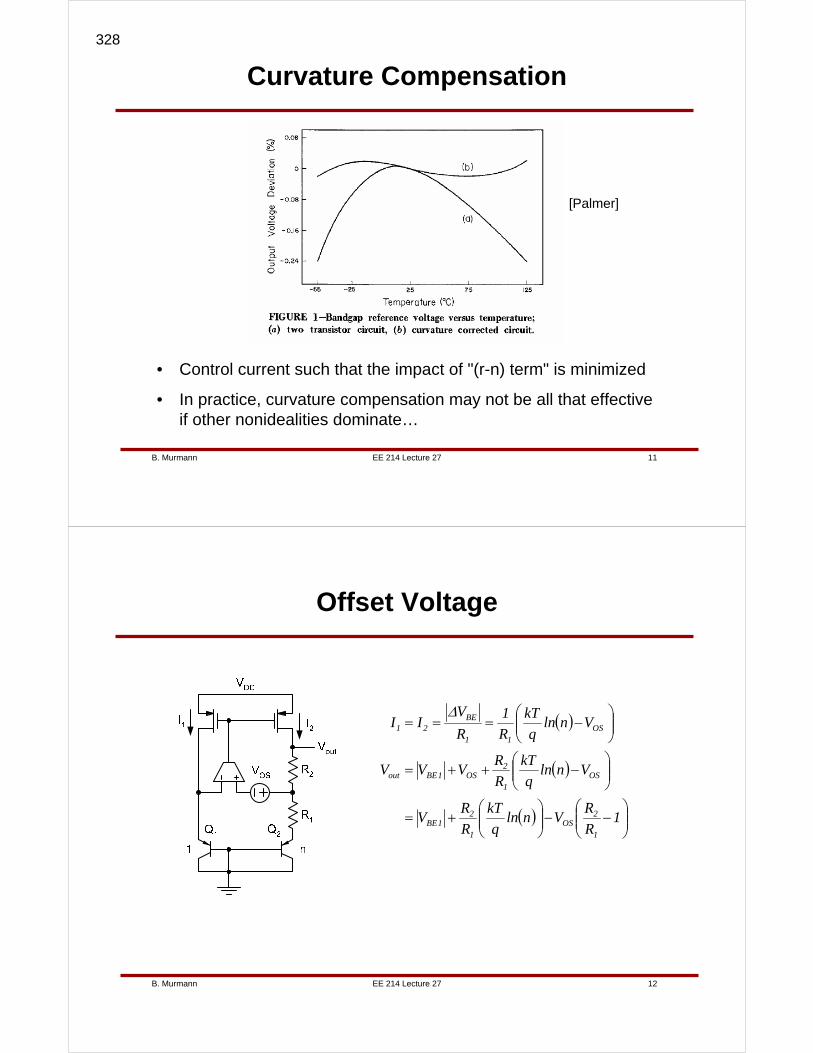
EE 214 Lecture 27B. Murmann 11
Curvature Compensation
• Control current such that the impact of "(r-n) term" is minimized
• In practice, curvature compensation may not be all that effective if other nonidealities dominate…
[Palmer]
EE 214 Lecture 27B. Murmann 12
Offset Voltage
( )
( )
( ) ⎟⎟⎠
⎞⎜⎜⎝
⎛−−⎟⎟
⎠
⎞⎜⎜⎝
⎛+=
⎟⎟⎠
⎞⎜⎜⎝
⎛−++=
⎟⎟⎠
⎞⎜⎜⎝
⎛−===
1R
RVnln
q
kT
R
RV
Vnlnq
kT
R
RVVV
Vnlnq
kT
R
1
R
VII
1
2OS
1
21BE
OS1
2OS1BEout
OS11
BE21
Δ
328

EE 214 Lecture 27B. Murmann 13
Issues
• VOS appears amplified at the bandgap output and can cause a large absolute error in Vout
– Since R2/R1-1 ≅ 8, this means that for VOS=5mV, the error in Vout will be about 40mV or roughly 3.3%
• If the bandgap is trimmed after manufacturing, e.g. to yield an output of VGO+2kT/q, then this is no longer the point of zero TC in presence of VOS
• In CMOS, VOS drift is typically 1…10μV/K– This means Vout will drift at least 8μV/K, which corresponds
to about 6.6 ppm/K• Good CMOS bandgaps achieve about 10…50ppm/K
• Possible solutions– Mitigate impact of offset by stacking two VBE
– Cancel offset or use low offset BJT differential pair
EE 214 Lecture 27B. Murmann 14
SC Bandgap with Offset Cancellation
[Nicollini]
329
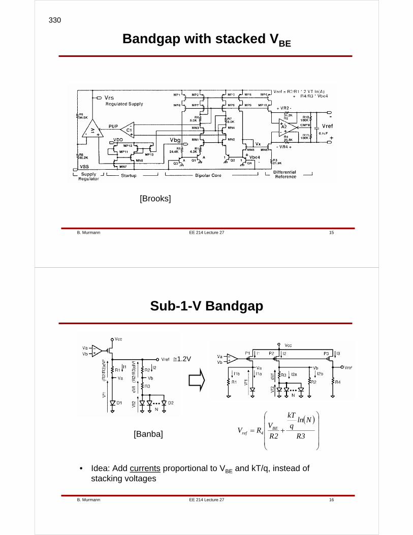
EE 214 Lecture 27B. Murmann 15
Bandgap with stacked VBE
[Brooks]
EE 214 Lecture 27B. Murmann 16
Sub-1-V Bandgap
• Idea: Add currents proportional to VBE and kT/q, instead of stacking voltages
≅1.2V
( )
⎟⎟⎟⎟
⎠
⎞
⎜⎜⎜⎜
⎝
⎛
+=3R
Nlnq
kT
2R
VRV BE
4ref[Banba]
330
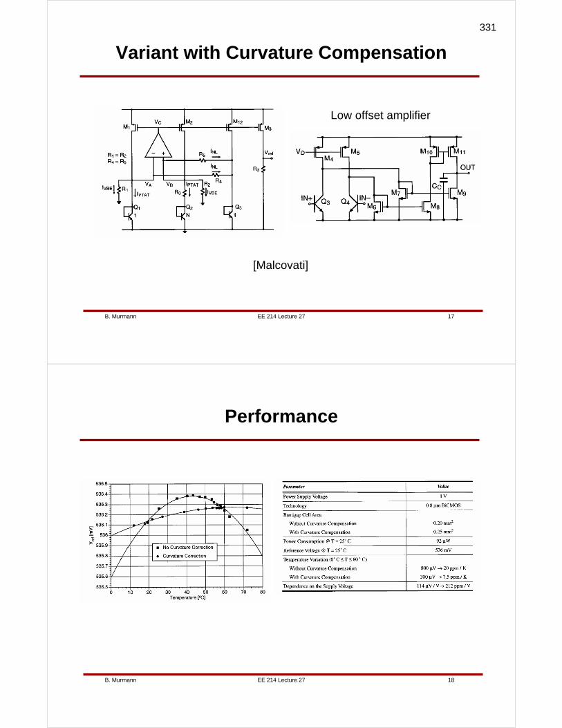
EE 214 Lecture 27B. Murmann 17
Variant with Curvature Compensation
[Malcovati]
Low offset amplifier
EE 214 Lecture 27B. Murmann 18
Performance
331

EE 214 Lecture 28B. Murmann 1
Lecture 28Technology Scaling
Boris MurmannStanford University
Copyright © 2007 by Boris Murmann
EE 214 Lecture 28B. Murmann 2
Overview
• Introduction
– The trend of continuously shrinking feature sizes in integrated circuits has resulted in enormous performance gains in both digital and analog circuits. However, since device scaling necessitates the use of smaller supply voltages, it is often argued that noise limited circuits can no longer benefit from scaling. In this lecture, we will take a closer look at this argument and also review basic analog device performance trends in light of feature size reduction.
332
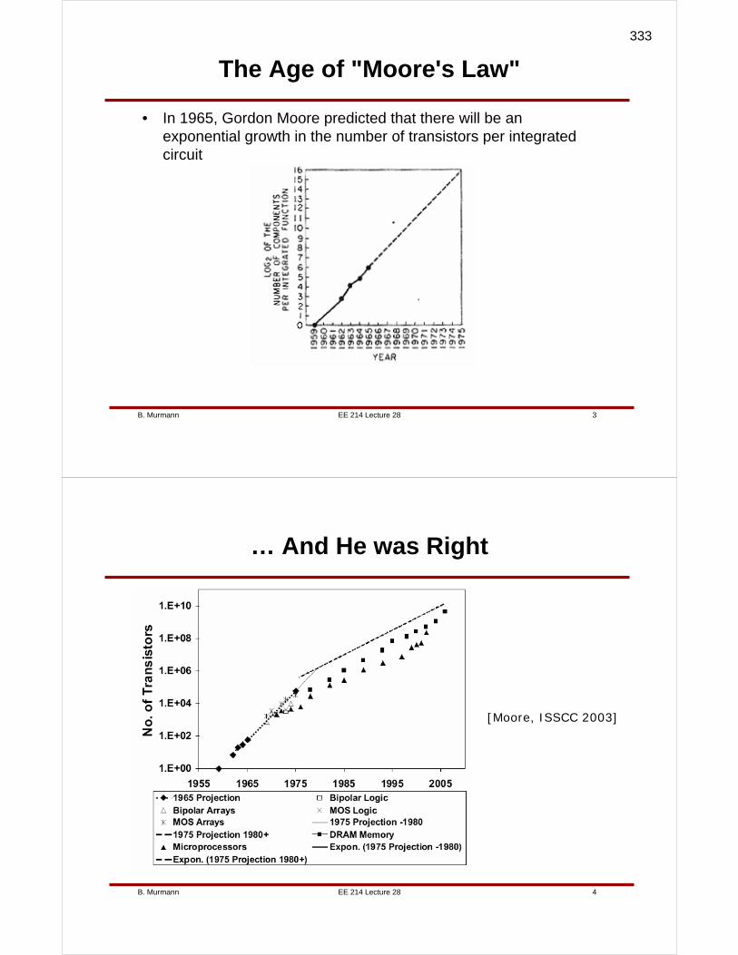
EE 214 Lecture 28B. Murmann 3
The Age of "Moore's Law"
• In 1965, Gordon Moore predicted that there will be an exponential growth in the number of transistors per integrated circuit
EE 214 Lecture 28B. Murmann 4
… And He was Right
[Moore, ISSCC 2003]
333
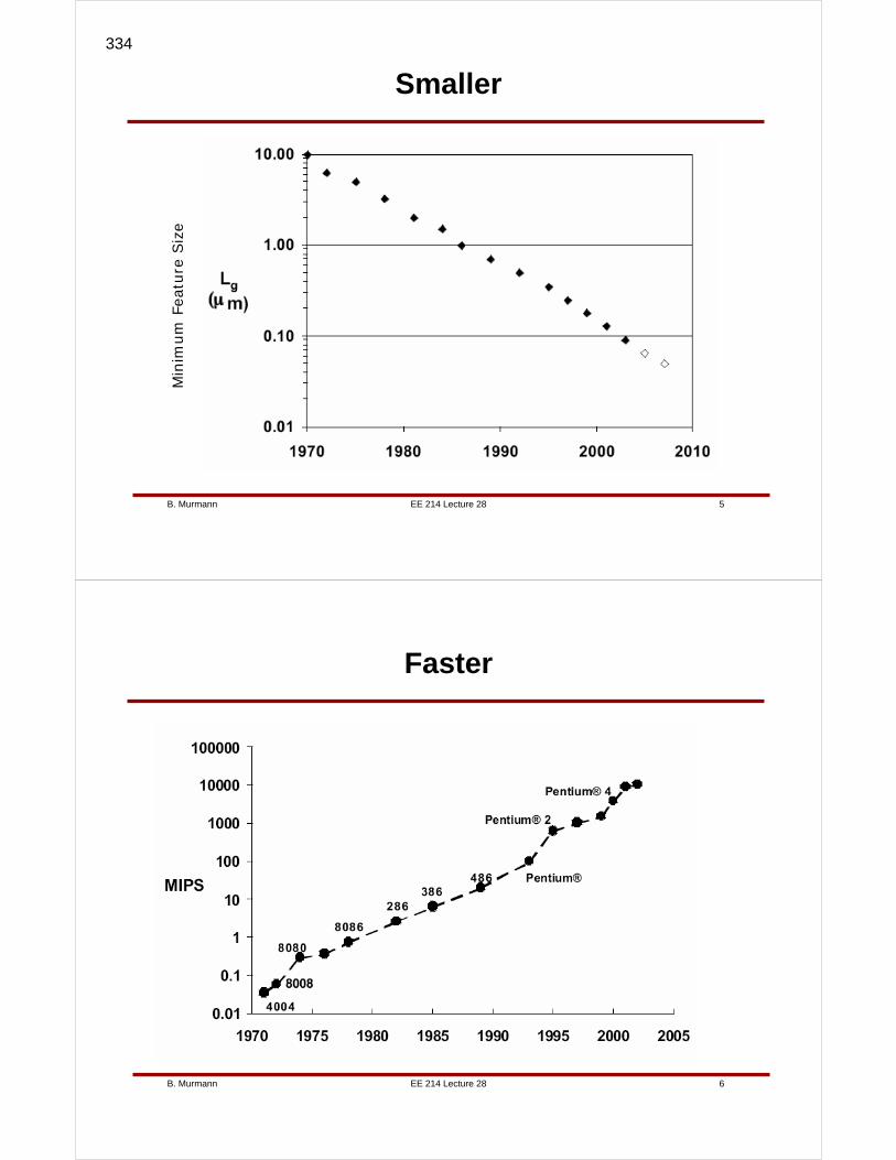
EE 214 Lecture 28B. Murmann 5
Smaller
Min
imum
Fea
ture
Siz
e
EE 214 Lecture 28B. Murmann 6
Faster
334
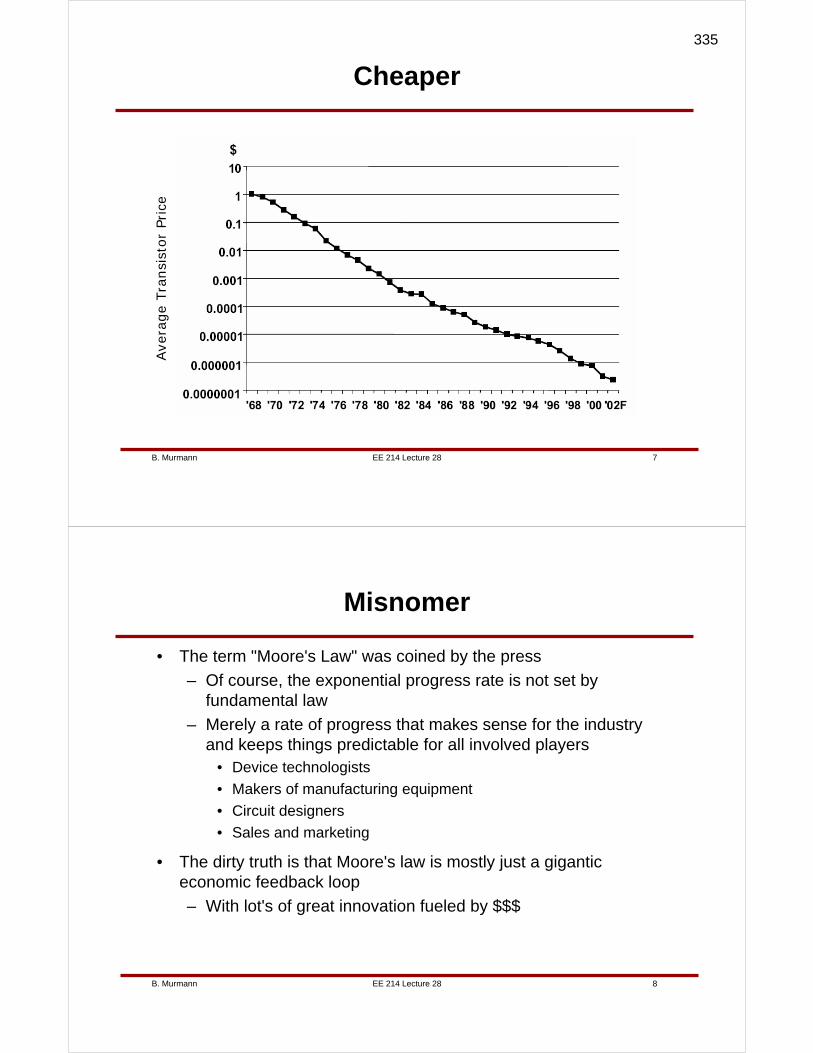
EE 214 Lecture 28B. Murmann 7
Cheaper
Ave
rage
Tra
nsi
stor
Pric
e
EE 214 Lecture 28B. Murmann 8
Misnomer
• The term "Moore's Law" was coined by the press
– Of course, the exponential progress rate is not set by fundamental law
– Merely a rate of progress that makes sense for the industry and keeps things predictable for all involved players
• Device technologists
• Makers of manufacturing equipment
• Circuit designers
• Sales and marketing
• The dirty truth is that Moore's law is mostly just a gigantic economic feedback loop
– With lot's of great innovation fueled by $$$
335
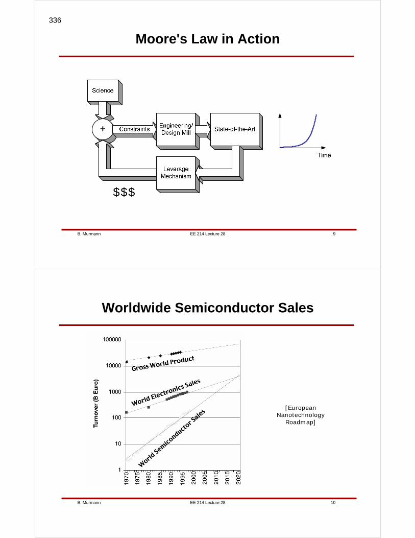
EE 214 Lecture 28B. Murmann 9
Moore's Law in Action
$$$
EE 214 Lecture 28B. Murmann 10
Worldwide Semiconductor Sales
[European Nanotechnology
Roadmap]
336

EE 214 Lecture 28B. Murmann 11
State-of-the-Art Semiconductor Fab
• Cost ~ $3,000,000,000
EE 214 Lecture 28B. Murmann 12
State-of-the-Art Silicon Technology
• 90nm feature sizes, electrical channel length of 50nm
• Gate oxide thickness 1.2nm, roughly 5 atomic layers
• 8 Layers of metal routing
337

EE 214 Lecture 28B. Murmann 13
State-of-the-Art Chips
Pentium 4 Processor, 125 Million Transistors[Schutz, ISSCC 2004]
Single-Chip 802.11 Transceiver
[Zargari, ISSCC 2004]
EE 214 Lecture 28B. Murmann 14
Impact of Technology Scaling
• Scaling is great from a digital perspective!
• Can show that scaling down features and voltages achieves three things simultaneously
– Higher speed
– More transistors/area
– Lower energy per operation
• How about analog circuits?
338

EE 214 Lecture 28B. Murmann 15
Quotes
• [Vertregt, ESSCIRC 2004]
– "Significant power efficiency improvements are predicted as a result of scaling to deep sub-micron technology nodes."
• [Annema, IEEE J. Solid-State Circuits, 12/2005 ]
– "In summary: unlike digital designs, analog circuits can benefit from technology scaling if the supply voltages are not scaled down."
• [Nauta, ESSCIRC 2005]
– "The evolution of CMOS technology will continue for many years to come, which is beneficial for digital circuits but which is not so for analog."
EE 214 Lecture 28B. Murmann 16
List of Concerns
• Reduced supply voltage
• Low intrinsic gain
• Variability
• Distortion
• Gate leakage
• Isolation
• …
• Cost (mask & wafer)
• Model accuracy
• …
339
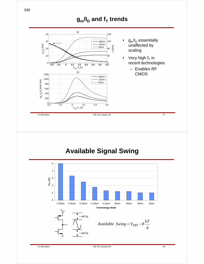
EE 214 Lecture 28B. Murmann 17
gm/ID and fT trends
• gm/ID essentially unaffected by scaling
• Very high fT in recent technologies
– Enables RF CMOS
-0.4 -0.2 0 0.2 0.4 0.60
200
400
600
800
1000
1200(b)
VGS
-Vt [V]
(gm
/I D)*
f T [G
Hz*
S/A
]
-0.2 -0.1 0 0.1 0.2 0.3 0.4 0.5 0.60
10
20
30
40(a)
gm
/I D [S
/A]
VGS
-Vt [V]
-0.2 -0.1 0 0.1 0.2 0.3 0.4 0.5 0.60
40
80
120
160
f T [G
Hz]
180nm130nm90nm
180nm130nm90nm
EE 214 Lecture 28B. Murmann 18
Available Signal Swing
0
1
2
3
4
5
0.50um 0.35um 0.25um 0.18um 0.12um 90nm 65nm 45nm 32nm
Technology Node
VD
D [
V]
> 4kT/q
> 4kT/q
VDD
q
kT8V SwingAvailable DD −<
340
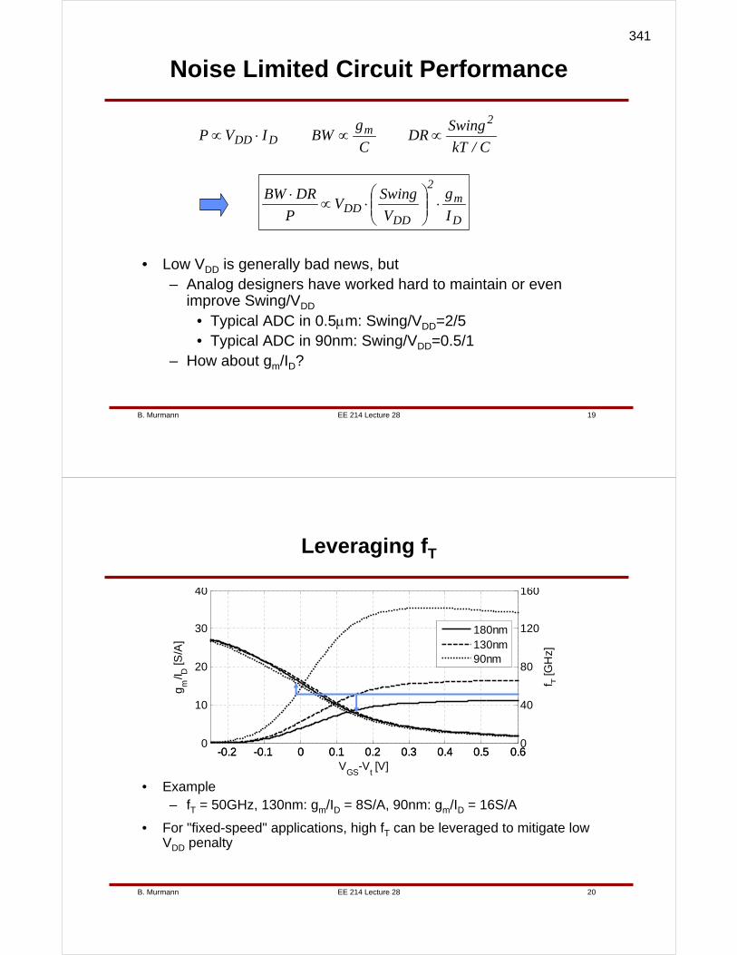
EE 214 Lecture 28B. Murmann 19
Noise Limited Circuit Performance
C/kT
SwingDR
C
gBWIVP
2m
DDD ∝∝⋅∝
D
m2
DDDD I
g
V
SwingV
P
DRBW⋅⎟⎟
⎠
⎞⎜⎜⎝
⎛⋅∝
⋅
• Low VDD is generally bad news, but– Analog designers have worked hard to maintain or even
improve Swing/VDD
• Typical ADC in 0.5μm: Swing/VDD=2/5• Typical ADC in 90nm: Swing/VDD=0.5/1
– How about gm/ID?
EE 214 Lecture 28B. Murmann 20
Leveraging fT
• Example– fT = 50GHz, 130nm: gm/ID = 8S/A, 90nm: gm/ID = 16S/A
• For "fixed-speed" applications, high fT can be leveraged to mitigate low VDD penalty
-0.2 -0.1 0 0.1 0.2 0.3 0.4 0.5 0.60
10
20
30
40
gm
/I D [S
/A]
VGS
-Vt [V]
-0.2 -0.1 0 0.1 0.2 0.3 0.4 0.5 0.60
40
80
120
160
f T [G
Hz]
180nm130nm90nm
341
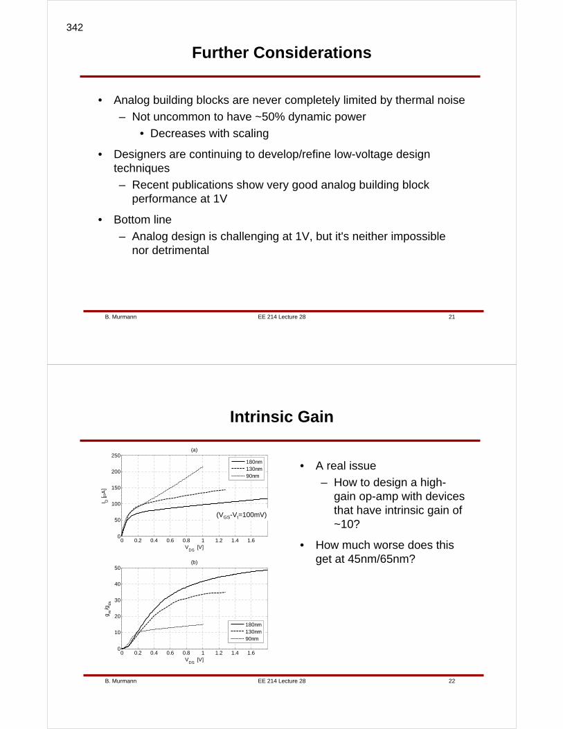
EE 214 Lecture 28B. Murmann 21
Further Considerations
• Analog building blocks are never completely limited by thermal noise
– Not uncommon to have ~50% dynamic power
• Decreases with scaling
• Designers are continuing to develop/refine low-voltage design techniques
– Recent publications show very good analog building block performance at 1V
• Bottom line
– Analog design is challenging at 1V, but it's neither impossible nor detrimental
EE 214 Lecture 28B. Murmann 22
Intrinsic Gain
• A real issue
– How to design a high-gain op-amp with devices that have intrinsic gain of ~10?
• How much worse does this get at 45nm/65nm?
0 0.2 0.4 0.6 0.8 1 1.2 1.4 1.60
50
100
150
200
250(a)
VDS
[V]
I D [ μ
A]
0 0.2 0.4 0.6 0.8 1 1.2 1.4 1.60
10
20
30
40
50(b)
VDS
[V]
gm
/gd
s
180nm130nm90nm
180nm130nm90nm
(VGS-Vt=100mV)
342
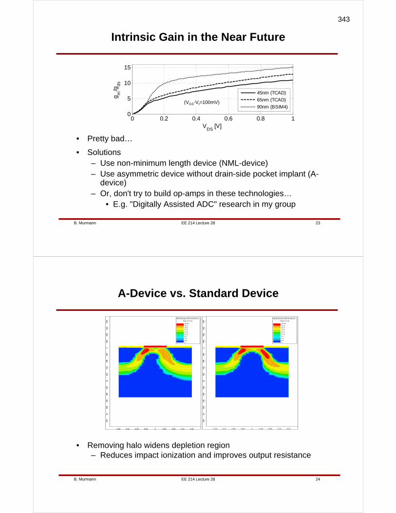
EE 214 Lecture 28B. Murmann 23
Intrinsic Gain in the Near Future
• Pretty bad…
• Solutions– Use non-minimum length device (NML-device)– Use asymmetric device without drain-side pocket implant (A-
device)– Or, don't try to build op-amps in these technologies…
• E.g. "Digitally Assisted ADC" research in my group
0 0.2 0.4 0.6 0.8 10
5
10
15
VDS
[V]
gm
/gd
s
45nm (TCAD)
65nm (TCAD)
90nm (BSIM4)(VGS-Vt=100mV)
EE 214 Lecture 28B. Murmann 24
A-Device vs. Standard Device
HoleImpactIonizationSigned Log
0
2.9
5.8
8.7
11.6
14.5
17.4
20.3
23.2
26.52
-0.16 -0.12 -0.08 -0.04 0 0.04 0.08 0.12 0.16
-0.1
6-0
.12
-0.0
8-0
.04
00.
040.
080.
120.
160.
20.
240.
280.
320.
360.
40.
44
HoleImpactIonizationSigned Log
0
2.9
5.8
8.7
11.6
14.5
17.4
20.3
23.2
26.58
-0.16 -0.12 -0.08 -0.04 0 0.04 0.08 0.12 0.16
-0.1
6-0
.12
-0.0
8-0
.04
00.
040.
080.
120.
160.
20.
240.
280.
320.
360.
40.
44
• Removing halo widens depletion region– Reduces impact ionization and improves output resistance
343
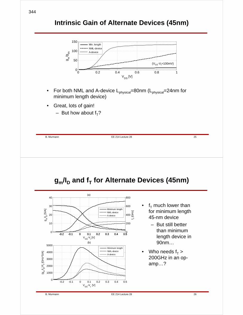
EE 214 Lecture 28B. Murmann 25
Intrinsic Gain of Alternate Devices (45nm)
• For both NML and A-device Lphysical=80nm (Lphysical=24nm for minimum length device)
• Great, lots of gain!
– But how about fT?
(VGS-Vt=100mV)
0 0.2 0.4 0.6 0.8 10
50
100
150( )
VDS
[V]
gm
/gd
s
Min. length
NML-device
A-device
(VGS-Vt=100mV)
EE 214 Lecture 28B. Murmann 26
gm/ID and fT for Alternate Devices (45nm)
• fT much lower than for minimum length 45-nm device
– But still better than minimum length device in 90nm…
• Who needs fT > 200GHz in an op-amp…?
-0.2 -0.1 0 0.1 0.2 0.3 0.4 0.50
1000
2000
3000
4000
5000(b)
VGS
-Vt [V]
(gm
/I D)*
f T [G
Hz*
S/A
]
-0.2 -0.1 0 0.1 0.2 0.3 0.4 0.50
10
20
30
40(a)
VGS
-Vt [V]
gm
/I D [S
/A]
-0.2 -0.1 0 0.1 0.2 0.3 0.4 0.50
200
400
600
800
f T [G
Hz]
Minimum length
NML-device
A-device
Minimum length
NML-device
A-device
344
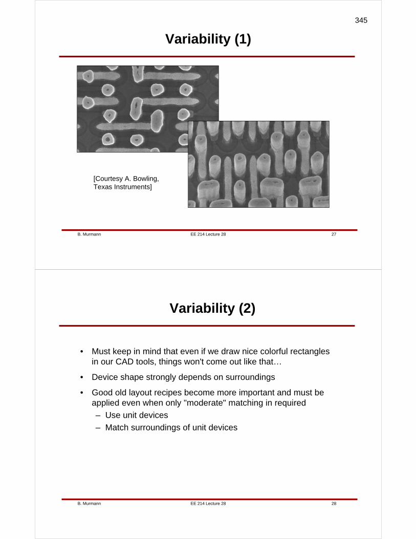
EE 214 Lecture 28B. Murmann 27
Variability (1)
[Courtesy A. Bowling, Texas Instruments]
EE 214 Lecture 28B. Murmann 28
Variability (2)
• Must keep in mind that even if we draw nice colorful rectangles in our CAD tools, things won't come out like that…
• Device shape strongly depends on surroundings
• Good old layout recipes become more important and must be applied even when only "moderate" matching in required
– Use unit devices
– Match surroundings of unit devices
345
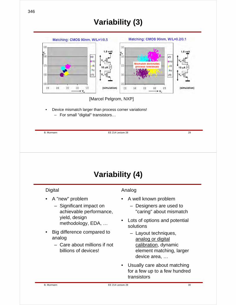
EE 214 Lecture 28B. Murmann 29
Variability (3)
• Device mismatch larger than process corner variations!– For small "digital" transistors…
[Marcel Pelgrom, NXP]
EE 214 Lecture 28B. Murmann 30
Variability (4)
Analog
• A well known problem
– Designers are used to "caring" about mismatch
• Lots of options and potential solutions
– Layout techniques, analog or digital calibration, dynamic element matching, larger device area, …
• Usually care about matching for a few up to a few hundred transistors
Digital
• A "new" problem
– Significant impact on achievable performance, yield, design methodology, EDA, …
• Big difference compared to analog
– Care about millions if not billions of devices!
346
EE 214 Lecture 28B. Murmann 31
An Interesting Hike Lies Ahead…
Bag of Tricks
A
D
EE 214 Lecture 28B. Murmann 32
Cost – The "Real" End of The Roadmap?
• Reference point: 30 mm2 die in 0.12μm CMOS
[Marcel Pelgrom, NXP]
347
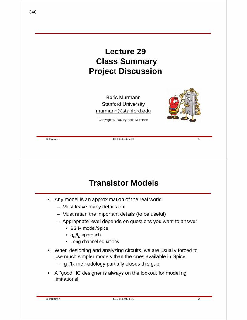
EE 214 Lecture 29B. Murmann 1
Lecture 29Class Summary
Project Discussion
Boris MurmannStanford University
Copyright © 2007 by Boris Murmann
EE 214 Lecture 29B. Murmann 2
Transistor Models
• Any model is an approximation of the real world
– Must leave many details out
– Must retain the important details (to be useful)
– Appropriate level depends on questions you want to answer• BSIM model/Spice
• gm/ID approach
• Long channel equations
• When designing and analyzing circuits, we are usually forced to use much simpler models than the ones available in Spice
– gm/ID methodology partially closes this gap
• A "good" IC designer is always on the lookout for modeling limitations!
348
EE 214 Lecture 29B. Murmann 3
Transistor Figures of Merit
• Transit Frequency
gg
mT C
g=ω
• Current Efficiency
D
m
I
g
• Intrinsic Gain
ds
m
g
g
EE 214 Lecture 29B. Murmann 4
Circuit Analysis
• Once we have appropriate models, we can in principle analyze any circuit using KCL/KVL
– Usually too difficult and also won’t allow us to reason about design choices and tradeoffs
• Crutches for circuit analysis
– Small signal approximation
– Zero value time constant method
– Miller approximation
– Return ratio analysis
– Blackman's impedance formula
– …
• Again, a good designer will always be on the lookout for potential limitations of the respective analysis method
349

EE 214 Lecture 29B. Murmann 5
The "Atoms" of Analog Circuit Design
• Common source
– Basic voltage amplifier
• Common gate
– Good for "shielding"
– Can help boost output impedance, mitigate Miller effect
• Common drain
– Buffer, level shifter
• Differential pair
EE 214 Lecture 29B. Murmann 6
Feedback (1)
• Desensitizes circuit to (forward-) gain variations
• Modifies port impedances
• Central quantity of interest: Loop gain T
– Quantifies static error
– Used to assess stability, phase and/or gain margin
– Helpful in calculating closed loop port impedances
• Finding T is simple
– E.g. break loop at transconductor, inject test current, calculate ratio of return and test current
• Typically need a dominant pole
– Hard to use more than 2-3 amplifier stages and maintain sufficient phase margin
350
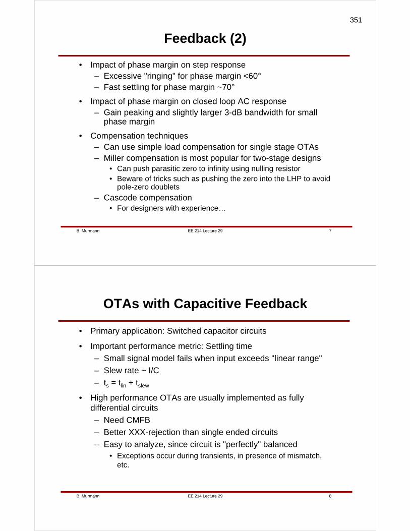
EE 214 Lecture 29B. Murmann 7
Feedback (2)
• Impact of phase margin on step response – Excessive "ringing" for phase margin <60°– Fast settling for phase margin ~70°
• Impact of phase margin on closed loop AC response– Gain peaking and slightly larger 3-dB bandwidth for small
phase margin
• Compensation techniques– Can use simple load compensation for single stage OTAs– Miller compensation is most popular for two-stage designs
• Can push parasitic zero to infinity using nulling resistor• Beware of tricks such as pushing the zero into the LHP to avoid
pole-zero doublets
– Cascode compensation• For designers with experience…
EE 214 Lecture 29B. Murmann 8
OTAs with Capacitive Feedback
• Primary application: Switched capacitor circuits
• Important performance metric: Settling time
– Small signal model fails when input exceeds "linear range"
– Slew rate ~ I/C
– ts = tlin + tslew
• High performance OTAs are usually implemented as fully differential circuits
– Need CMFB
– Better XXX-rejection than single ended circuits
– Easy to analyze, since circuit is "perfectly" balanced• Exceptions occur during transients, in presence of mismatch,
etc.
351

EE 214 Lecture 29B. Murmann 9
Electronic Noise
• Tends to set achievable power dissipation in circuits with high DR requirements
• Fundamental noise
– Thermal noise
• Technology related noise
– 1/f noise
• Increasing (noise limited) precision by "one bit" quadruples power dissipation!
EE 214 Lecture 29B. Murmann 10
References
• Self-biasing concept
– Beware of stability issues!
• Current references
– VDD, VGS, ΔVGS, VBE, ΔVBE - based approaches
– To first order, ΔVGS bias yields constant gm over temperature and process
• Voltage reference
– Bandgap
– Useful as a reference whenever there's a need to convert "bits to Volts" or "Volts to bits"
– Conceptually simple, but lots of second order issues
352