green's function integral equation methods for plasmonic...
TRANSCRIPT
1
Green's function integral equation methods for plasmonic nanostructures
(PhD Course: Optical at the Nanoscale)
Thomas Søndergaard
Department of Physics and Nanotechnology, Aalborg University,
Skjernvej 4A, DK-9220 Aalborg Øst, Denmark
1. Introduction to Green's functions in electromagnetics
Consider the task of solving an inhomogeneous operator equation of the form
𝜃𝜑 = 𝑗, (1)
where is the operator, j is a source term, and is the function we want to calculate. This type of equation
can be straightforwardly solved when a Green's function [1,2] of the operator exists and is known. A
Green's function g of a given operator is a solution to the equation
𝜃𝑔 = 𝐼, (2)
where I is the unit operator, and consequently a solution to Eq. (1) is given straightforwardly by
𝜑 = 𝑔𝑗. (3)
Other solutions can be obtained by addition of a solution to the homogeneous equation (Eq. (1) with j=0) or
by using Eq. (3) but with another choice of Green's function.
One approach to the construction of a Green’s function in the case that is a Hermitian operator with a
complete set of orthonormal eigenfunctions |𝜑𝑛 satisfying 𝜃 |𝜑𝑛 = 𝑛 |𝜑𝑛 is
𝑔 = |𝜑𝑛 𝜑𝑛 |
𝑛𝑛 (4)
A convenient method for electromagnetics purposes of adding a homogeneous solution is to use Eq. (4)
where we add a very small imaginary part i*s to the denominator and observe the transition of 𝑠 → ±0, and
apply lim𝑠→01
𝑥+𝑖𝑠= 𝑃
1
𝑥− 𝑖𝜋𝛿(𝑥) . Depending on the sign of s when taking the limit we obtain either the
advanced or the retarded Green’s function.
Green's function related to the electrostatic potential:
A well-known inhomogeneous differential equation in electrostatics for the electric potential is
∇2𝜑(𝒓) = −𝜌(𝒓)/𝜖0, (5)
where is the charge density distribution, and 𝜖0 is the vacuum permittivity. The equally well-known
particular solution to this equation is given by
2
𝜑(𝒓) = 1
4𝜋 𝒓−𝒓′ 𝜌(𝒓′)/𝜖0𝑑
3𝑟′. (6)
Although the concept of the Green's function is usually not mentioned in relation to the method of
calculating the potential in Eq. (6) this equation is an example of Eq. (3) with the Green's function 𝑔 𝒓, 𝒓′ =1
4𝜋 𝒓−𝒓′ , which satisfies ∇2𝑔 𝒓, 𝒓′ = −𝛿 𝒓 − 𝒓′ , i.e. in this case 𝛿 𝒓 − 𝒓′ is the unit operator.
Green's function of the operator of the 1D, 2D and 3D Helmholtz equation:
The macroscopic monochromatic electric field 𝑬 = 𝑬(𝒓)𝑒𝑖𝜔𝑡 generated by a monochromatic current
distribution 𝑱 = 𝑱(𝒓)𝑒𝑖𝜔𝑡 satisfies the Helmholtz equation
∇2 + k02 𝑬(𝒓) = 𝑖𝜔𝜇0𝑱(𝒓), (7)
where k0 = ω/c, and c is the vacuum speed of light. In addition, if we assume that there are no free charges,
the electric field must satisfy ∇ ∙ 𝐄 = 0. A particularly simple situation is the one-dimensional case of
propagation in only one dimension, e.g. along the x-axis, with field and current vectors pointing
perpendicular to the x-axis, and varying only along the x-axis, e.g. 𝑬(𝒓) = 𝑦 𝐸(𝑥) and 𝑱(𝒓) = 𝑦 𝐽(𝑥), in
which case the requirement ∇ ∙ 𝐄 = 0 is automatically satisfied, and Eq. (7) reduces to
𝑑2
𝑑𝑥 2+ k0
2 𝐸(𝑥) = 𝑖𝜔𝜇0𝐽(𝑥).
(8)
The relevant Green’s function in this case must be a solution to
𝑑2
𝑑𝑥 2+ k0
2 𝑔 𝑥, 𝑥′ = −𝛿(𝑥 − 𝑥′), (9)
and it is straightforward to show that a solution is given by
𝑔 𝑥, 𝑥′ =1
2𝑖𝑘0𝑒−𝑖𝑘0 𝑥−𝑥′ . (10)
Note that this particular Green’s function also satisfies the condition that it behaves as waves propagating
away from the “source point” x’, i.e. this is the retarded Green’s function. Thus, solutions to Eq. (7) obtained
by
𝐸 𝑥 = −𝑖𝜔𝜇0 𝑔 𝑥, 𝑥′ 𝐽(𝑥′)𝑑𝑥′
(11)
satisfy the radiating boundary condition, i.e. that the waves generated by the sources J should propagate
away from the sources.
For propagation in two dimensions and s-polarisation, i.e. the electric field (and currents) is perpendicular to
the plane of propagation, the condition ∇ ∙ 𝐄 = 0 is also automatically satisfied. In this case the Helmholtz
equation becomes
𝜕2
𝜕𝑥 2+
𝜕2
𝜕𝑦 2+ k0
2 𝐸(𝑥,𝑦) = 𝑖𝜔𝜇0𝐽(𝑥,𝑦), (12)
3
The Green’s function related to the operator acting on E is given by
𝑔 𝑥,𝑦, 𝑥′ ,𝑦′ =1
4𝑖𝐻0(2)
22
0 '' yyxxk , (13)
where 𝐻0(2)
is the Hankel function of the second kind and order zero. The solution of interest is
𝐸 𝑥, 𝑦 = −𝑖𝜔𝜇0 𝑔 𝑥,𝑦, 𝑥′ ,𝑦′ 𝐽(𝑥′ ,𝑦′)𝑑𝑥′𝑑𝑦′. (14)
For completeness we will also mention the Green’s function for the 3D scalar Helmholtz equation
𝑔 𝒓, 𝒓′ =exp(−𝑖𝑘0 𝒓−𝒓
′ )
4𝜋 𝒓−𝒓′ , (15)
which satisfies
∇2 + k02 𝑔 𝒓, 𝒓′ = −𝛿(𝒓 − 𝒓′). (16)
In the 3D case the wave equation for the electric field can be written
∇2 + k02 𝑬 𝒓 = 𝑖𝜔𝜇0𝑱 𝒓 + ∇∇ ∙ 𝑬 𝒓 , (17)
in which case the result for the scalar 3D case can be applied to construct the following equation for E
𝑬 𝒓 = − 𝑔 𝒓, 𝒓′ 𝑖𝜔𝜇0𝑱 𝒓′ 𝑑3𝑟′ − 𝑔 𝒓, 𝒓′ ∇′∇′ ∙ 𝑬 𝒓′ 𝑑3𝑟′ . (18)
However, from Eq. (17) follows by taking the divergence on each side that
k02∇ ∙ 𝑬 𝒓 = 𝑖𝜔𝜇0∇ ∙ 𝑱 𝒓 , (19)
which when being combined with Eq. (18) leads to
𝑬 𝒓 = − 𝑔 𝒓, 𝒓′ 𝑖𝜔𝜇0𝐽 𝒓′ + 𝑔 𝒓, 𝒓′
1
𝑘02 𝑖𝜔𝜇0∇′∇′ ∙ 𝑱 𝒓
′ 𝑑3𝑟′ . (20)
This can be rewritten as
𝑬 𝒓 = −𝑖𝜔𝜇0 𝐺 𝒓, 𝒓′ ∙ 𝑱 𝒓′ 𝑑3𝑟′ (21)
in terms of the dyadic Green’s tensor
𝐺 𝒓, 𝒓′ = 𝑰 +1
𝑘02 ∇∇ 𝑔 𝒓, 𝒓′ , (22)
which is a solution to
−∇× ∇ × 𝐺 𝒓, 𝒓′ + 𝑘02𝐺 𝒓, 𝒓′ = −𝑰𝛿(𝒓 − 𝒓′). (23)
Exercise 1:
Construct the Green’s function (15) using Eq. (4).
4
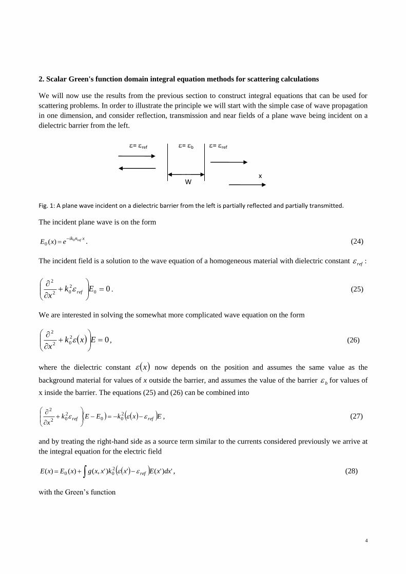
2. Scalar Green's function domain integral equation methods for scattering calculations
We will now use the results from the previous section to construct integral equations that can be used for
scattering problems. In order to illustrate the principle we will start with the simple case of wave propagation
in one dimension, and consider reflection, transmission and near fields of a plane wave being incident on a
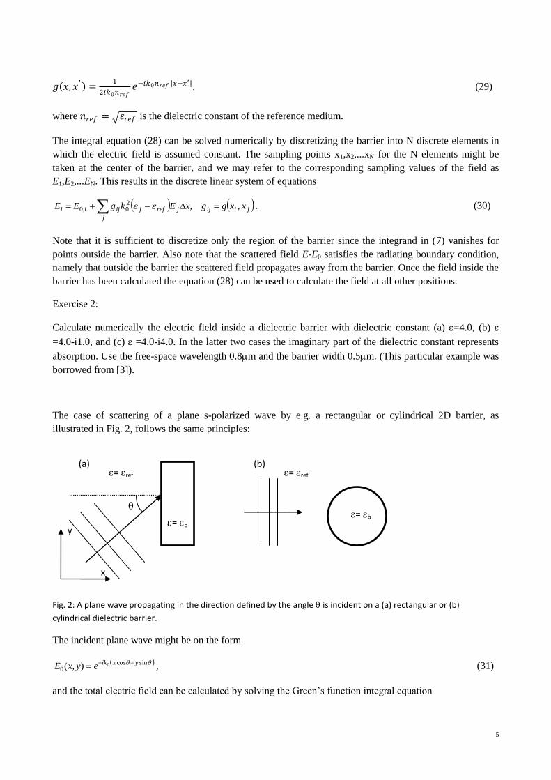
dielectric barrier from the left.
Fig. 1: A plane wave incident on a dielectric barrier from the left is partially reflected and partially transmitted.
The incident plane wave is on the form
xnik refexE 0)(0
. (24)
The incident field is a solution to the wave equation of a homogeneous material with dielectric constant ref :
00
2
02
2
Ek
xref . (25)
We are interested in solving the somewhat more complicated wave equation on the form
02
02
2
Exk
x , (26)
where the dielectric constant x now depends on the position and assumes the same value as the
background material for values of x outside the barrier, and assumes the value of the barrier b for values of
x inside the barrier. The equations (25) and (26) can be combined into
ExkEEkx
refref
200
202
2
, (27)
and by treating the right-hand side as a source term similar to the currents considered previously we arrive at
the integral equation for the electric field
')'(')',()()( 200 dxxExkxxgxExE ref , (28)
with the Green’s function
=ref
W x
=ref =b
5
𝑔 𝑥, 𝑥′ =1
2𝑖𝑘0𝑛𝑟𝑒𝑓𝑒−𝑖𝑘0𝑛𝑟𝑒𝑓 𝑥−𝑥′ , (29)
where 𝑛𝑟𝑒𝑓 = 휀𝑟𝑒𝑓 is the dielectric constant of the reference medium.
The integral equation (28) can be solved numerically by discretizing the barrier into N discrete elements in
which the electric field is assumed constant. The sampling points x1,x2,...xN for the N elements might be
taken at the center of the barrier, and we may refer to the corresponding sampling values of the field as
E1,E2,...EN. This results in the discrete linear system of equations
jiij
j
jrefjijii xxggxEkgEE ,,20,0 . (30)
Note that it is sufficient to discretize only the region of the barrier since the integrand in (7) vanishes for
points outside the barrier. Also note that the scattered field E-E0 satisfies the radiating boundary condition,
namely that outside the barrier the scattered field propagates away from the barrier. Once the field inside the
barrier has been calculated the equation (28) can be used to calculate the field at all other positions.
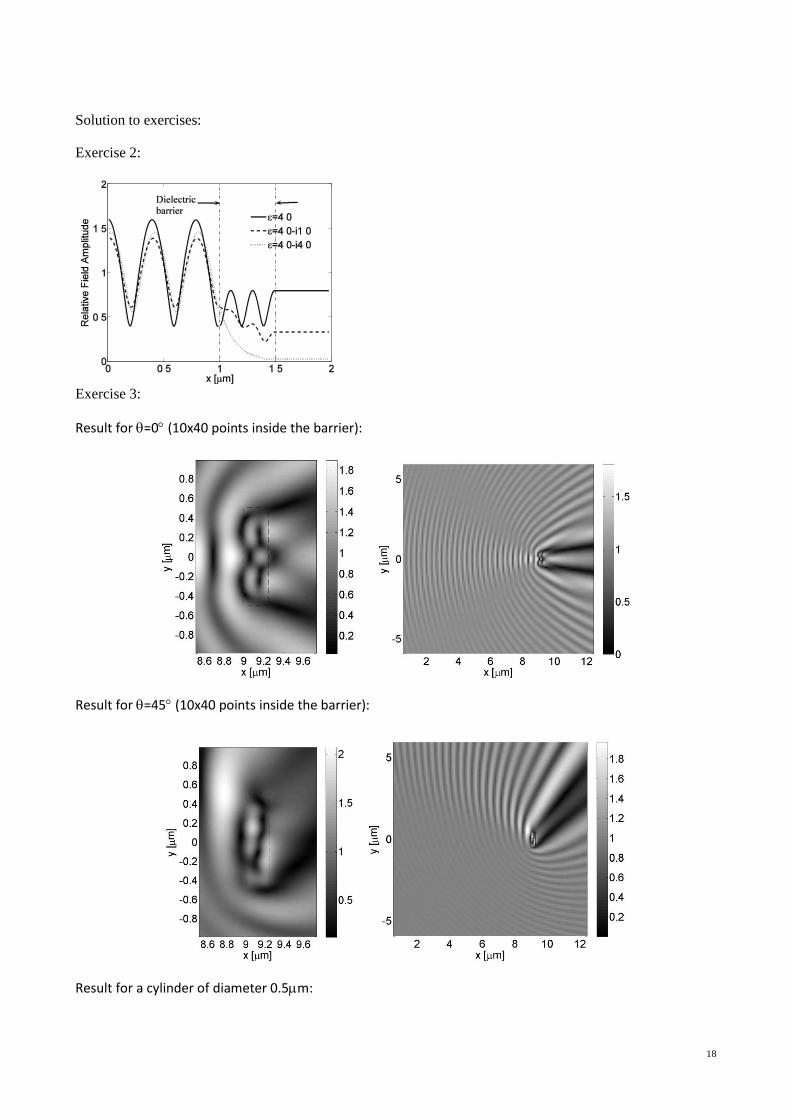
Exercise 2:
Calculate numerically the electric field inside a dielectric barrier with dielectric constant (a) =4.0, (b)
=4.0-i1.0, and (c) =4.0-i4.0. In the latter two cases the imaginary part of the dielectric constant represents
absorption. Use the free-space wavelength 0.8m and the barrier width 0.5m. (This particular example was
borrowed from [3]).
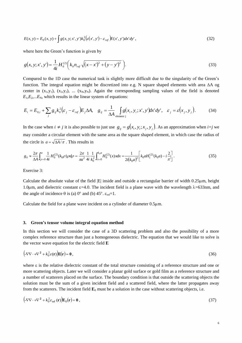
The case of scattering of a plane s-polarized wave by e.g. a rectangular or cylindrical 2D barrier, as
illustrated in Fig. 2, follows the same principles:
Fig. 2: A plane wave propagating in the direction defined by the angle is incident on a (a) rectangular or (b)
cylindrical dielectric barrier.
The incident plane wave might be on the form
sincos0
0),(yxik
eyxE
, (31)
and the total electric field can be calculated by solving the Green’s function integral equation
=ref
=b
=ref
x
y
(a) (b)
=b
6
'')','(',')',';,(),(),( 200 dydxyxEyxkyxyxgyxEyxE ref , (32)
where here the Green’s function is given by
22
0
)2(
0 ''4
1',';, yyxxnkH
iyxyxg ref . (33)
Compared to the 1D case the numerical task is slightly more difficult due to the singularity of the Green’s
function. The integral equation might be discretized into e.g. N square shaped elements with area A og
center in (x1,y1), (x2,y2), ... (xN,yN). Again the corresponding sampling values of the field is denoted
E1,E2,...EN, which results in the linear system of equations:
jjjiiij
j
jrefjijii yxdydxyxyxgA
gAEkgEE ,,''',';,1
,jelement
2
0,0
. (34)
In the case when 𝑖 ≠ 𝑗 it is also possible to just use jjiiij yxyxgg ,;, . As an approximation when i=j we
may consider a circular element with the same area as the square shaped element, in which case the radius of
the circle is /Aa . This results in
2)(
2
1)(
1
4
12)(
4
120
)2(102
00
)2(02
02
00
)2(0
0
iakaHkaki
xdxxHkia
dkHiA
gak
x
a
ii . (35)
Exercise 3:
Calculate the absolute value of the field |E| inside and outside a rectangular barrier of width 0.25m, height
1.0m, and dielectric constant =4.0. The incident field is a plane wave with the wavelength =633nm, and
the angle of incidence is (a) 0 and (b) 45. ref=1.
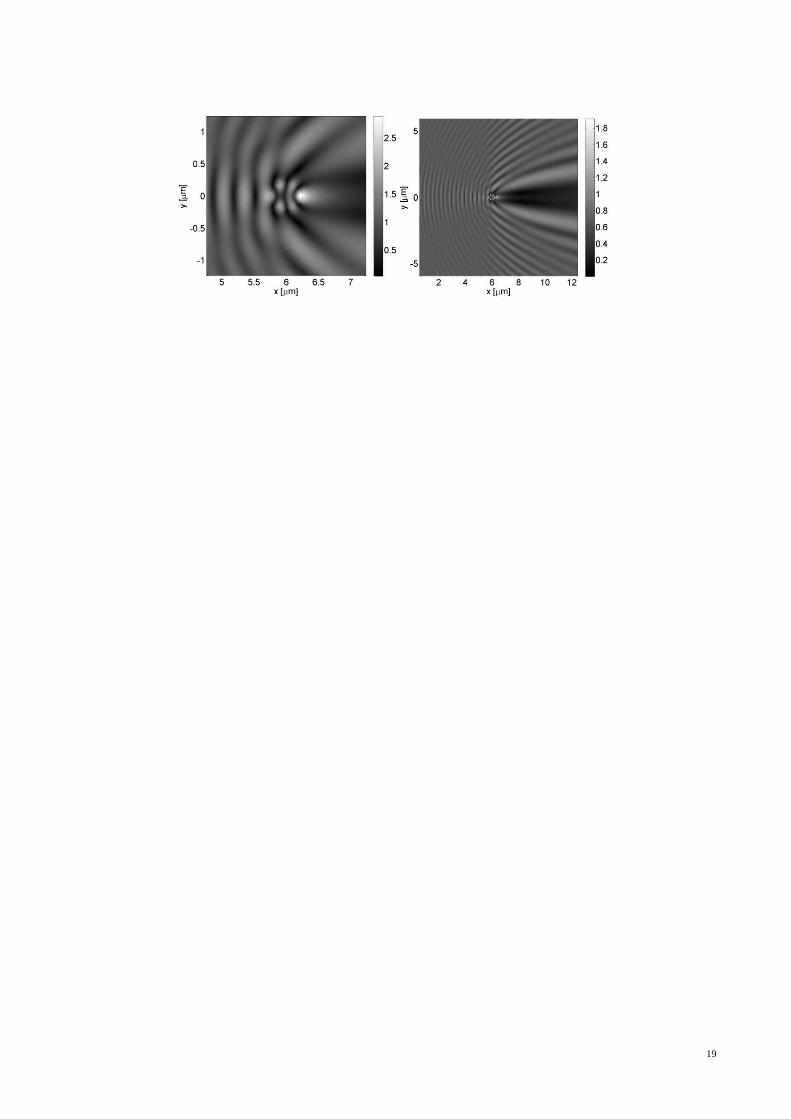
Calculate the field for a plane wave incident on a cylinder of diameter 0.5m.
3. Green’s tensor volume integral equation method
In this section we will consider the case of a 3D scattering problem and also the possibility of a more
complex reference structure than just a homogeneous dielectric. The equation that we would like to solve is
the vector wave equation for the electric field E
0rEr2 )(2
0k- , (36)
where is the relative dielectric constant of the total structure consisting of a reference structure and one or
more scattering objects. Later we will consider a planar gold surface or gold film as a reference structure and
a number of scatterers placed on the surface. The boundary condition is that outside the scattering objects the
solution must be the sum of a given incident field and a scattered field, where the latter propagates away
from the scatterers. The incident field E0 must be a solution in the case without scattering objects, i.e.
0rEr2 0ref
20 )(k- , (37)
7
where ref is the relative dielectric constant for the reference structure, e.g. the planar gold surface without
gold scatterers on the surface.
A Green’s tensor G for the reference structure is defined as a solution to the equation
)'(',)(ref
2
0 rrIrrGr2 k- , (38)
where is the Dirac delta function, and I is the unit tensor. Compared to previous sections we allow ref to
depend on the position.
Similar to previous sections we can rewrite Eqs. (1) and (2) into
rErrrErEr2 )()()( ref
200ref
20 kk- , (39)
which results in the vector integral equation
''''', 3ref
200 rdk rErrrrGrErE . (40)
The scattered field component will satisfy the radiating boundary condition for a proper choice of Green’s
tensor. It is possible to e.g. use as a reference structure the planar metal surface, a metal film, or a more
complex structure, without additional numerical costs, if the reference structure Green’s tensor G is known.
Only in the case of a homogeneous reference medium can we obtain a simple analytical expression for the
Green’s tensor. If the dielectric constant in this case is ref(r)=n2, where n is the refractive index (k=k0n), the
Green’s tensor G=GD is given by
'','4
','1
' 2
'
2
Drrrr
rrrrrrIrrG
2
rr
D
ik
DD gke
ggk
.
(41)
This leads to the following analytic and highly singular Green’s tensor
''
3
'
31
'
''
'
1
'1'
22222
Drr
rrrrrr
rrrr
rrrrIrrG
Dg
kk
i
kk
i. (42)
For a reference structure consisting of planar metal-dielectric interface or metal film the Green’s tensor can
be constructed e.g. by expanding the homogeneous medium Green’s tensor in terms of an in-plane wave
number kx, and for each kx add a term for z>0 which accounts for reflection, and by constructing a
transmitted term for z<0 such that the electromagnetics boundary conditions are fulfilled at the interface [4],
which for source and observation points with z,z’>0 results in
0',,ˆˆˆˆˆˆˆˆ
ˆˆˆˆˆˆ4
';'
)'(
1
2'0
1
''0
2
'0
2
1''
0
'0
1
3
002
S
1
zzerkJJk
rJzzi
rJJ
rJzzdk
izz
zzis
zz
p
pz
p
z
z
ρρG
, (43)
8
where rp and r
s are the Fresnel reflection coefficients for p- and s-polarized waves, respectively, kz1=(k
2-kx
2)
½
with Im(kz1)0, and ’ are the projections of r and r’ on the xy-plane, =|’|, and , and z are
coordinate unit vectors in a cylindrical coordinate system centered at ’, i.e '/'ˆ ρρρρ . J0 is the
Bessel function of order 0, and ’ means differentiation with respect to the argument. The Fresnel reflection
coefficients are functions of k.
One approach to solve Eq. (40) is to discretize the scatterer into N volume elements where the field and the
dielectric “constant” are assumed constant. This leads to a linear system of equations of the form
j
jjjijii EGEE ref,,0 , (44)
where
'', 320 rdki
Vij
j
rrGG . (45)
The latter integral over the Green’s tensor is rather difficult in the case where i=j due to the singularity of the
Green’s tensor. In particular, if an exclusion volume is placed around the singularity when carrying out the
integral (45), and the limit of the exclusion volume going to zero is observed, the result will depend on the
shape of the exclusion volume. For very small volume elements and i=j the expression (45) only depends on
the shape of the volume element Vi and not the size. It has been tabulated for various shapes in Ref. [5]. One
method of handling the singularity is to convert the volume integral into a surface integral [6], where the
surfaces are placed away from the singularity. For the homogeneous medium Green’s tensor this is done by
using Eqs. (41) and then applying Green’s theorem resulting in
''''ˆ''ˆ 2sdgnniV
iD
ii srIIG , (46)
where iV is the surface of volume element i, and n is the outward surface normal vector.
The approach of Eqs. (40) and (41) is equivalent to the Discrete Dipole Approximation method (DDA)
introduced by Purcell and Pennypacker in 1973 [7] if we restrict sampling points and volume elements to be
placed on a cubic lattice, and treat each volume element as a point dipole with a polarizability equivalent to a
small sphere with the same dielectric constant and the same volume as the cubic volume element it has
replaced. In this sense the DDA is equivalent to using
jiVkjiij ,, 20rrGG . (47)
Regarding the case i=j Purcell and Pennypacker used the equivalent of Gii=-I/(3ref). Later it was remarked
e.g. by Draine [8] that in order for a (dielectric) dipole to not oscillate exactly in phase with the incident field
it is necessary to include an imaginary part being equivalent to using Gii=-I(1/3+ik3V/6)/ref. Both
expressions are good approximations to Eqs. (45).
We may notice that in the case of a homogeneous reference medium the Green’s tensor depends only on the
difference r-r’, in which case Eq. (40) is a convolution integral. In the case of the DDA, or when using
volume elements of the same size and shape placed on a lattice, Eq. (40) takes the form of a discrete
convolution, i.e.
9
zyx
zyxzyxzzyyxxzyxzyx
jjj
jjjjjjD
jijijiiiiiii
,,
,,ref,,,,,,,0,, EGEE . (48)
Rather than solving Eq. (48) using Gaussian elimination, LU-decomposition etc. and similar schemes with
calculation time proportional to N3, it might seem advantageous to solve the equation using an iterative
approach where a trial vector is optimized until a convergence criteria is satisfied (see e.g. [8]). This
procedure involves many matrix-vector multiplications (convolutions) of the form in Eq. (48). By calculating
the convolution by first applying the Fast Fourier Transform (FFT), multiplying in reciprocal space, and then
applying the FFT once more the calculation time (due to the FFTs) can be reduced to being proportional to
NlogN if the number of grid points along each axis is a power of 2. Furthermore, the storage for the matrix is
reduced to scale as N. From these considerations it appears that both in terms of calculation time and
computer memory requirements it is desirable to use e.g. cubic volume elements of the same size and shape
placed on a cubic lattice (or the DDA). In the case of a planar metal-dielectric interface reference structure
Eq. (48) will also contain a summation over GS depending on iz+jz instead of iz-jz. This case can also be
carried out using the FFT with resulting calculation time ~ NlogN. Actually, one major drawback of using
cubic elements of the same size and shape is that the surface of curved structures will be represented with a
stair-cased surface, which seems to result in slow convergence, or worse, as we shall see an example of in
the next section.
4. Green’s tensor area integral equation method
In the case of propagation in only 2D and p-polarization we are faced with the same complexity as in the
previous section, namely that the vector components of the field are coupled, and a vector integral equation
is required. We assume that the structure and electromagnetic fields are invariant along the z-axis, and
propagation is in the xy-plane. The electric field is given by yyxxEyEx yxˆˆ,)(ˆ)(ˆ)( rrrrE .
The integral equation is except for a d2r’ instead of d
3r’ equivalent to the 3D integral equation, i.e.
''''', 2ref
200 rdk rErrrrGrErE . (49)
The 2D Green’s tensor is required here, and for a homogeneous reference medium it can be calculated
analytically, i.e.
'4
',',1
',',)2(
02
Drrrr,rrIrrGrrG
kH
igg
k
DD . (50)
Discretization and numerical solution follows the same principles as considered previously.
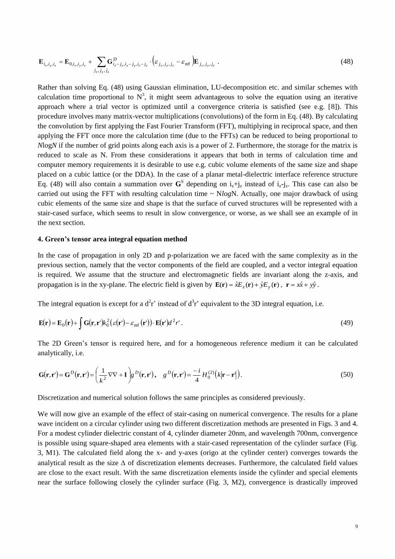
We will now give an example of the effect of stair-casing on numerical convergence. The results for a plane
wave incident on a circular cylinder using two different discretization methods are presented in Figs. 3 and 4.
For a modest cylinder dielectric constant of 4, cylinder diameter 20nm, and wavelength 700nm, convergence
is possible using square-shaped area elements with a stair-cased representation of the cylinder surface (Fig.
3, M1). The calculated field along the x- and y-axes (origo at the cylinder center) converges towards the
analytical result as the size of discretization elements decreases. Furthermore, the calculated field values
are close to the exact result. With the same discretization elements inside the cylinder and special elements
near the surface following closely the cylinder surface (Fig. 3, M2), convergence is drastically improved
10
using practically the same number of elements. In this case the elements of type M1 leads to the correct
result but much slower compared to using the elements of type M2.
(a) (b)
Fig. 3: Total field along the (a) x-axis and (b) y-axis through the center of a circular cylinder with dielectric constant 4
(background dielectric constant 1) and diameter 20nm. A p-polarized plane wave with wavelength 700nm is incident
along the x-axis. M1: calculation using only square area elements. M2: the same square area elements are used inside
the cylinder, and special elements are used near the surface following closely the actual cylinder surface (see inset).
is the side length of the square area elements. The solid line is the analytical and exact result.
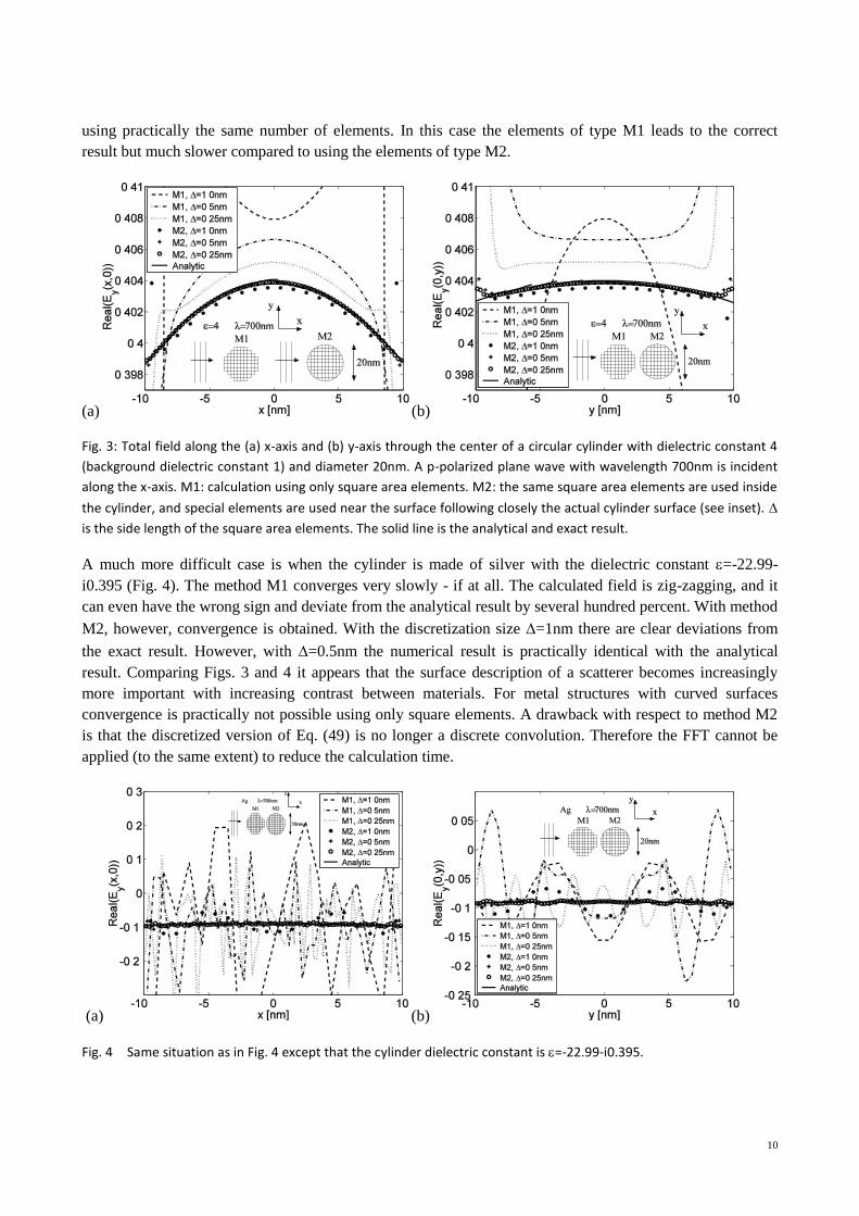
A much more difficult case is when the cylinder is made of silver with the dielectric constant =-22.99-
i0.395 (Fig. 4). The method M1 converges very slowly - if at all. The calculated field is zig-zagging, and it
can even have the wrong sign and deviate from the analytical result by several hundred percent. With method
M2, however, convergence is obtained. With the discretization size =1nm there are clear deviations from
the exact result. However, with =0.5nm the numerical result is practically identical with the analytical
result. Comparing Figs. 3 and 4 it appears that the surface description of a scatterer becomes increasingly
more important with increasing contrast between materials. For metal structures with curved surfaces
convergence is practically not possible using only square elements. A drawback with respect to method M2
is that the discretized version of Eq. (49) is no longer a discrete convolution. Therefore the FFT cannot be
applied (to the same extent) to reduce the calculation time.
(a) (b)
Fig. 4 Same situation as in Fig. 4 except that the cylinder dielectric constant is =-22.99-i0.395.
11
These examples illustrate that for a high contrast between the involved dielectric constants the numerical
treatment of the surface of the structure requires serious consideration.
Similar to the 3D case the Green’s tensor for a metal surface or metal film can be constructed by adding
wave solutions to the homogeneous medium Green’s tensor such that boundary conditions are satisfied at the
metal surfaces. The scalar homogeneous medium Green’s function can be expanded in the following way
0)Im(,,'cos1
2', 222
0
'
yyxx
yyi
xy
D kdexxi
gx
y
rr . (51)
An expansion of GD in in-plane wave numbers kx is then obtained by applying the operator in Eq. (50) to Eq.
(51). For each kx a reflection term must then be added, and elsewhere a transmission term must be
constructed such that the electric field boundary conditions are fulfilled for each kx. In the case of the source
point r’ placed above the metal film (y’>0) the Green’s tensor for y>0 becomes G(r,r’)= GD(r,r’) + G
S(r,r’),
where
0
'
22)'(cos
1ˆˆˆˆ)'(sinˆˆˆˆ
2',
x
y
x
yyiPx
y
y
xxS derxxyy
kxxxxi
kxyyx
i
rrG ,(52)
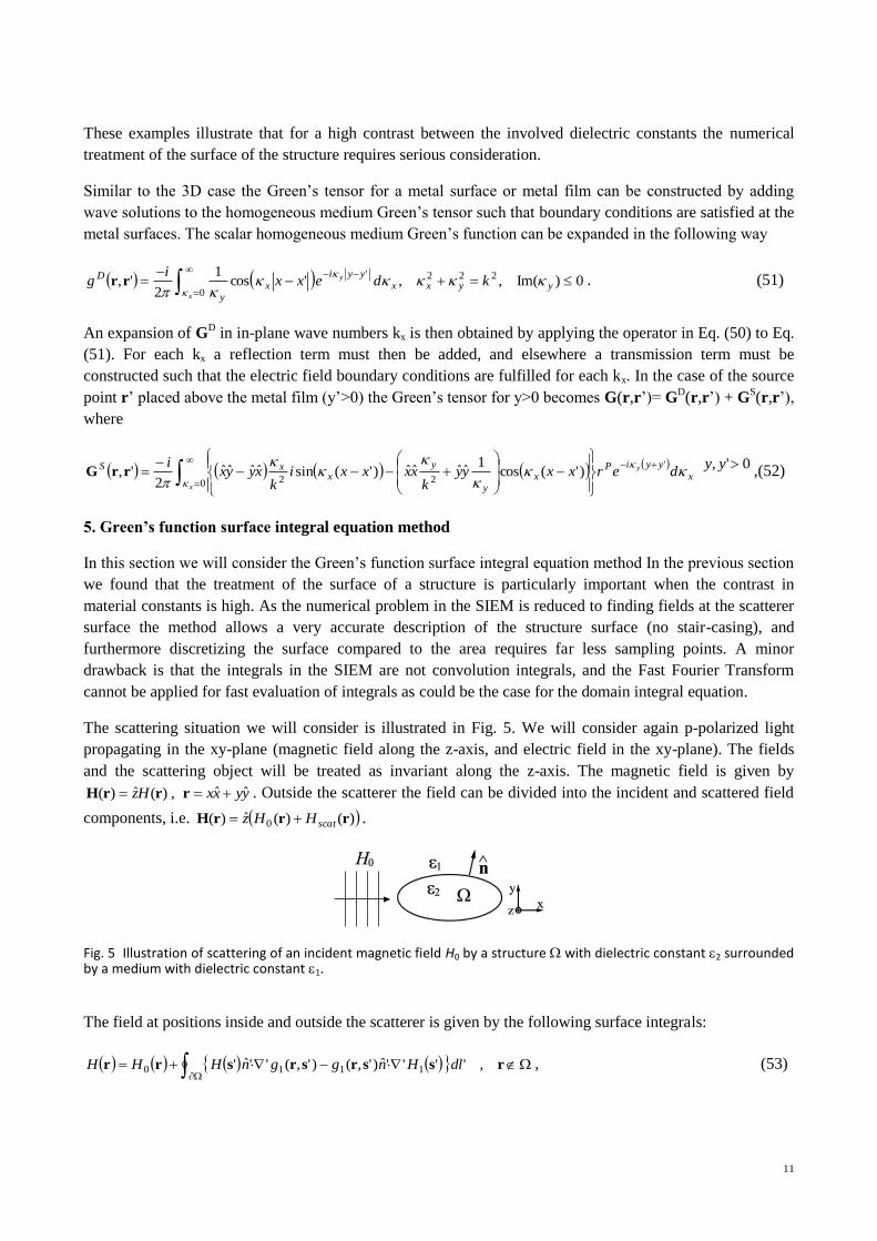
5. Green’s function surface integral equation method
In this section we will consider the Green’s function surface integral equation method In the previous section
we found that the treatment of the surface of a structure is particularly important when the contrast in
material constants is high. As the numerical problem in the SIEM is reduced to finding fields at the scatterer
surface the method allows a very accurate description of the structure surface (no stair-casing), and
furthermore discretizing the surface compared to the area requires far less sampling points. A minor
drawback is that the integrals in the SIEM are not convolution integrals, and the Fast Fourier Transform
cannot be applied for fast evaluation of integrals as could be the case for the domain integral equation.
The scattering situation we will consider is illustrated in Fig. 5. We will consider again p-polarized light
propagating in the xy-plane (magnetic field along the z-axis, and electric field in the xy-plane). The fields
and the scattering object will be treated as invariant along the z-axis. The magnetic field is given by
yyxxHz ˆˆ,)(ˆ)( rrrH . Outside the scatterer the field can be divided into the incident and scattered field
components, i.e. )()(ˆ)( 0 rrrH scatHHz .
Fig. 5 Illustration of scattering of an incident magnetic field H0 by a structure with dielectric constant 2 surrounded by a medium with dielectric constant 1.
The field at positions inside and outside the scatterer is given by the following surface integrals:
rssrsrsrr ,''''ˆ)',()',(''ˆ' 1110 dlHnggnHHH , (53)
0', yy
12
rssrsrsr ,''''ˆ)',()',(''ˆ' 1
1
222 dlHnggnHH
, (54)
where the Green’s function ikHg 4/')',( 2,10)2(
02,1 rrrr , and n is the outward surface normal vector.
The subscript “1” in '''ˆ 1 sHn indicates that this is the normal derivative of the magnetic field approaching
the surface from medium “1”. In Eq. (54) the electromagnetics boundary conditions have been applied to
replace '''ˆ 2 sHn with 121 /'''ˆ sHn . Eq. (54) follows directly from applying Gauss’ theorem to its right-
hand side and transforming the curve integral into an area integral and then applying
)'()',()( 2,12,120
2rrrr gk and 0)())(( 2
02 rr Hk . Eq. (53) follows from considering an equation
similar to Eq. (54) for the total field over a domain bounded by the surface of and a circular surface C
placed at infinity. For a position r placed far from C we may advantageously split the surface integral over
C into an integral over H0 and an integral over Hscat. The first integral gives H0(r), and the latter vanishes
since Hscat satisfies the radiating boundary condition. We note that Hscat = H-H0 does in fact satisfy this
boundary condition at C due to the nature of the Green’s function chosen (see Eq. (53)). Before Eqs. (53,54)
can be applied we have to find the field and its normal derivative at the surface. Self-consistent equations can
be obtained from Eqs. (53,54) by letting r approach the surface from either side, in which case we deal with
the singularity of )',(''ˆ 2,1 srgn in the limit of r approaching a point s on the surface by rewriting the integrals
as principal value integrals, where the singularity for a smooth surface gives a contribution of 2/)(sH
depending on from which side the surface is approached, i.e.
''''ˆ)',()',(''ˆ'
2
11110 dlHnggnHPHH ssssssss , (55)
''''ˆ)',()',(''ˆ'2
11
1
222 dlHnggnHPH sssssss
, (56)
where P refers to the principal value. These equations are discretized such that the surface is divided into a
finite number of segments on which H and 1ˆ Hn are assumed constant. Regarding the integrals in Eqs.
(55,56) the variation of )',(''ˆ 2,1 ssgn and )',(2,1 ssg can be taken into account by subdividing each segment in
e.g. 20 subsegments, which also allows describing more accurately the actual shape of the surface. The
electric field is obtained using )(ˆ)/()( 2,1 rrE Hzi and Eqs. (53,54). A few examples illustrating
convergence of the method applied to metallic nanostructures are presented in Fig. 6.
13
(a) (b)
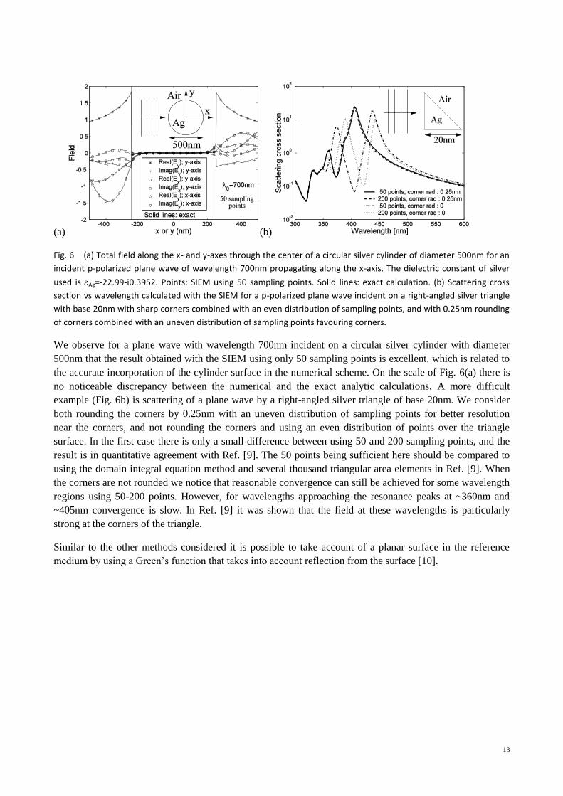
Fig. 6 (a) Total field along the x- and y-axes through the center of a circular silver cylinder of diameter 500nm for an
incident p-polarized plane wave of wavelength 700nm propagating along the x-axis. The dielectric constant of silver
used is Ag=-22.99-i0.3952. Points: SIEM using 50 sampling points. Solid lines: exact calculation. (b) Scattering cross
section vs wavelength calculated with the SIEM for a p-polarized plane wave incident on a right-angled silver triangle
with base 20nm with sharp corners combined with an even distribution of sampling points, and with 0.25nm rounding
of corners combined with an uneven distribution of sampling points favouring corners.
We observe for a plane wave with wavelength 700nm incident on a circular silver cylinder with diameter
500nm that the result obtained with the SIEM using only 50 sampling points is excellent, which is related to
the accurate incorporation of the cylinder surface in the numerical scheme. On the scale of Fig. 6(a) there is
no noticeable discrepancy between the numerical and the exact analytic calculations. A more difficult
example (Fig. 6b) is scattering of a plane wave by a right-angled silver triangle of base 20nm. We consider
both rounding the corners by 0.25nm with an uneven distribution of sampling points for better resolution
near the corners, and not rounding the corners and using an even distribution of points over the triangle
surface. In the first case there is only a small difference between using 50 and 200 sampling points, and the
result is in quantitative agreement with Ref. [9]. The 50 points being sufficient here should be compared to
using the domain integral equation method and several thousand triangular area elements in Ref. [9]. When
the corners are not rounded we notice that reasonable convergence can still be achieved for some wavelength
regions using 50-200 points. However, for wavelengths approaching the resonance peaks at ~360nm and
~405nm convergence is slow. In Ref. [9] it was shown that the field at these wavelengths is particularly
strong at the corners of the triangle.
Similar to the other methods considered it is possible to take account of a planar surface in the reference
medium by using a Green’s function that takes into account reflection from the surface [10].
14
6. Results obtained for plasmonic nanostructures using Green’s function integral equation methods
In this section we will consider modeling of plasmonic nanostructures related to three types of plasmonic
surface waves bound to and propagating along planar metal-dielectric interfaces (Fig. 7a), namely the surface
plasmon polariton (SPP) propagating along a single metal-dielectric interface, the long-range SPP (LR-SPP)
and the short-range SPP (SR-SPP) bound to and propagating along a thin (10-20nm) metal film [11]. The
three types of SPPs are p-polarized waves, i.e. when they propagate along the positive x-axis as in the
illustration in Fig. 7a the electric field only has an x- and a y-component. At least for SPPs and LR-SPPs, and
often for SR-SPPs at positions outside the metal, the electric field is dominated by the y-component (Ey)
illustrated in Fig. 7a. The propagation length is limited by ohmic losses. It depends on the type of SPP and
the metal film thickness. For SPPs and wavelength 1550nm the intensity is e.g. reduced by a factor e after
propagating 61m along an interface between gold and a polymer with refractive index 1.54. For LR-SPPs
and a 15nm gold film the corresponding length is 6mm, equivalent to thousands of wavelengths, which is
enough to make these waves interesting for integrated optics [12,13]. LR-SPPs are, however, loosely bound
with most of the field located outside the metal film. The SR-SPP on the other hand is strongly bound but
the propagation length is limited to a few free-space wavelengths.
By placing objects at the metal interfaces, or via film terminations, the SPP waves can be manipulated via
scattering processes, resulting in plasmonic devices e.g. for communication on an optical chip, signal
processing and sensing [14] (Fig. 7b). We will consider cylindrical gold scatterers arranged on a hexagonal
lattice on a gold surface (SPP bandgap structure) [12,15-17], periodically repeated gold ridges on either side
of a thin gold film (LR-SPP grating) [18-21], and a film of short length, i.e. a metal strip (SR-SPP resonator),
where SR-SPPs propagating back and forth form standing wave resonances [22-24]. SR-SPPs are contrary to
LR-SPPs efficiently reflected at strip terminations as they are strongly bound.
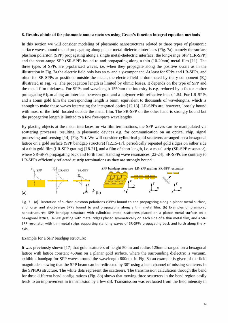
(a) (b)
Fig. 7 (a) Illustration of surface plasmon polaritons (SPPs) bound to and propagating along a planar metal surface,
and long- and short-range SPPs bound to and propagating along a thin metal film. (b) Examples of plasmonic
nanostructures: SPP bandgap structure with cylindrical metal scatterers placed on a planar metal surface on a
hexagonal lattice, LR-SPP grating with metal ridges placed symmetrically on each side of a thin metal film, and a SR-
SPP resonator with thin metal strips supporting standing waves of SR-SPPs propagating back and forth along the x-
axis.
Example for a SPP bandgap structure:
It was previously shown [17] that gold scatterers of height 50nm and radius 125nm arranged on a hexagonal
lattice with lattice constant 450nm on a planar gold surface, where the surrounding dielectric is vacuum,
exhibit a bandgap for SPP waves around the wavelength 800nm. In Fig. 8a an example is given of the field
magnitude showing that the SPP beam can be redirected by 30 using a bent channel of missing scatterers in
the SPPBG structure. The white dots represent the scatterers. The transmission calculation through the bend
for three different bend configurations (Fig. 8b) shows that moving three scatterers in the bend region easily
leads to an improvement in transmission by a few dB. Transmission was evaluated from the field intensity in
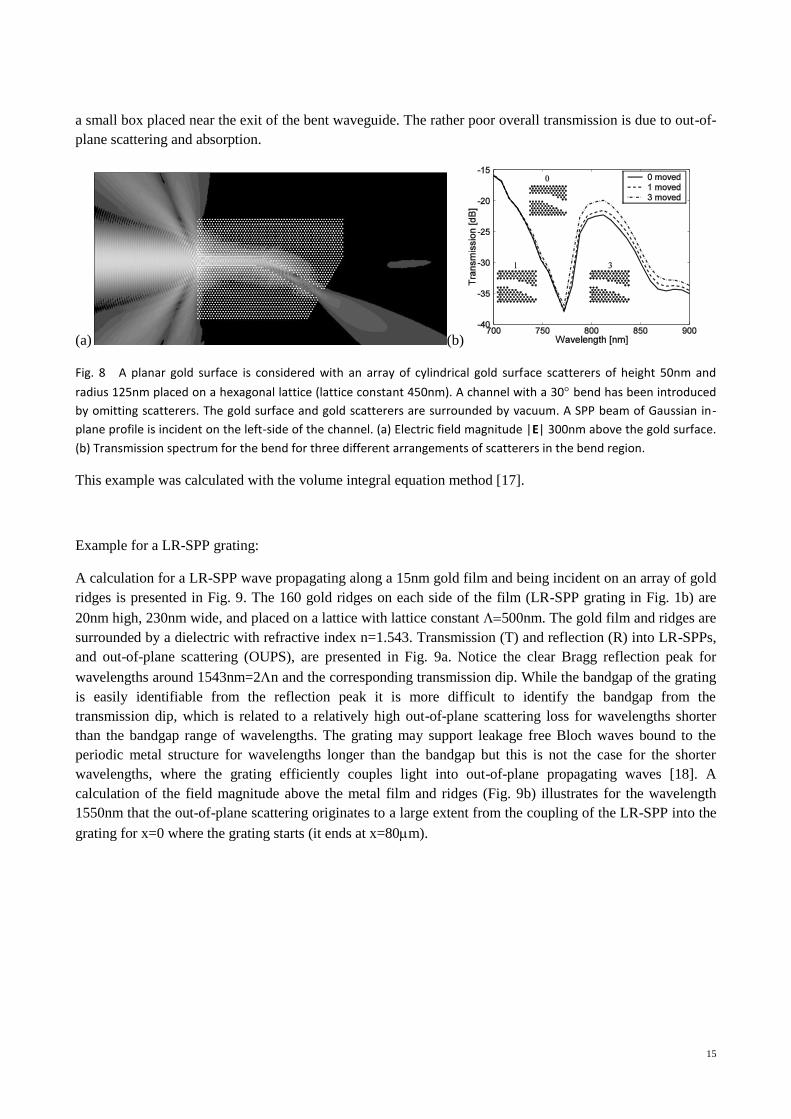
15
a small box placed near the exit of the bent waveguide. The rather poor overall transmission is due to out-of-
plane scattering and absorption.
(a) (b)
Fig. 8 A planar gold surface is considered with an array of cylindrical gold surface scatterers of height 50nm and
radius 125nm placed on a hexagonal lattice (lattice constant 450nm). A channel with a 30 bend has been introduced
by omitting scatterers. The gold surface and gold scatterers are surrounded by vacuum. A SPP beam of Gaussian in-
plane profile is incident on the left-side of the channel. (a) Electric field magnitude |E| 300nm above the gold surface.
(b) Transmission spectrum for the bend for three different arrangements of scatterers in the bend region.
This example was calculated with the volume integral equation method [17].
Example for a LR-SPP grating:
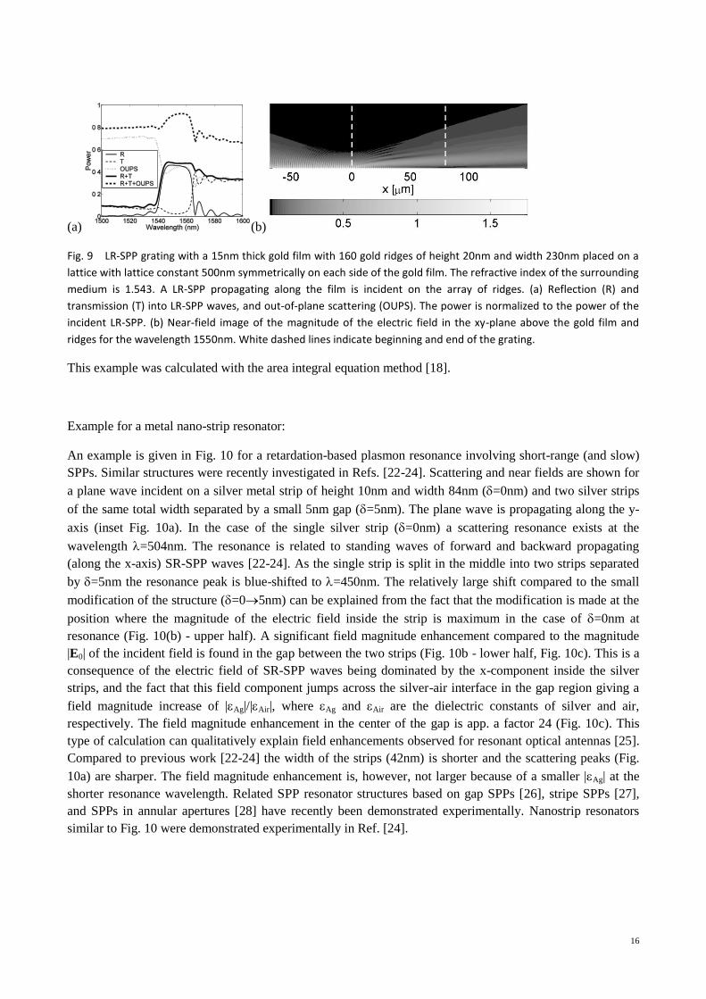
A calculation for a LR-SPP wave propagating along a 15nm gold film and being incident on an array of gold
ridges is presented in Fig. 9. The 160 gold ridges on each side of the film (LR-SPP grating in Fig. 1b) are
20nm high, 230nm wide, and placed on a lattice with lattice constant 500nm. The gold film and ridges are
surrounded by a dielectric with refractive index n=1.543. Transmission (T) and reflection (R) into LR-SPPs,
and out-of-plane scattering (OUPS), are presented in Fig. 9a. Notice the clear Bragg reflection peak for
wavelengths around 1543nm=2n and the corresponding transmission dip. While the bandgap of the grating
is easily identifiable from the reflection peak it is more difficult to identify the bandgap from the
transmission dip, which is related to a relatively high out-of-plane scattering loss for wavelengths shorter
than the bandgap range of wavelengths. The grating may support leakage free Bloch waves bound to the
periodic metal structure for wavelengths longer than the bandgap but this is not the case for the shorter
wavelengths, where the grating efficiently couples light into out-of-plane propagating waves [18]. A
calculation of the field magnitude above the metal film and ridges (Fig. 9b) illustrates for the wavelength
1550nm that the out-of-plane scattering originates to a large extent from the coupling of the LR-SPP into the
grating for x=0 where the grating starts (it ends at x=80m).
16
(a) (b)
Fig. 9 LR-SPP grating with a 15nm thick gold film with 160 gold ridges of height 20nm and width 230nm placed on a
lattice with lattice constant 500nm symmetrically on each side of the gold film. The refractive index of the surrounding
medium is 1.543. A LR-SPP propagating along the film is incident on the array of ridges. (a) Reflection (R) and
transmission (T) into LR-SPP waves, and out-of-plane scattering (OUPS). The power is normalized to the power of the
incident LR-SPP. (b) Near-field image of the magnitude of the electric field in the xy-plane above the gold film and
ridges for the wavelength 1550nm. White dashed lines indicate beginning and end of the grating.
This example was calculated with the area integral equation method [18].
Example for a metal nano-strip resonator:
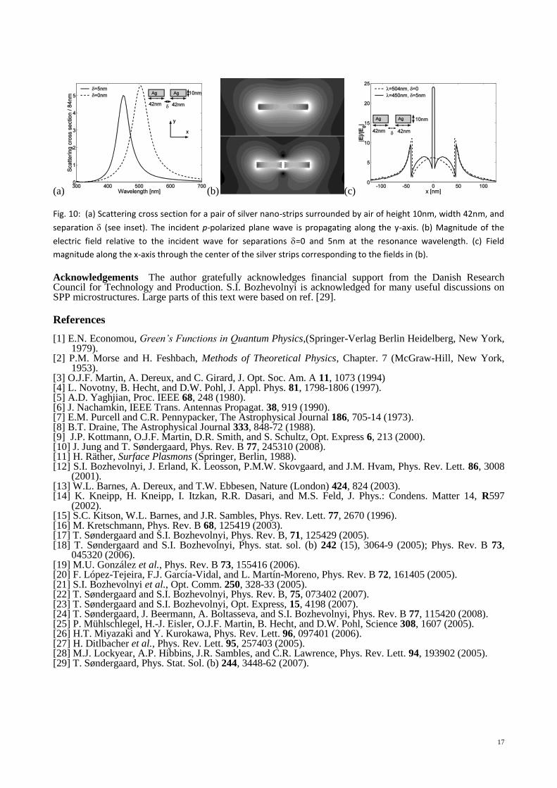
An example is given in Fig. 10 for a retardation-based plasmon resonance involving short-range (and slow)
SPPs. Similar structures were recently investigated in Refs. [22-24]. Scattering and near fields are shown for
a plane wave incident on a silver metal strip of height 10nm and width 84nm (=0nm) and two silver strips
of the same total width separated by a small 5nm gap (=5nm). The plane wave is propagating along the y-
axis (inset Fig. 10a). In the case of the single silver strip (=0nm) a scattering resonance exists at the
wavelength =504nm. The resonance is related to standing waves of forward and backward propagating
(along the x-axis) SR-SPP waves [22-24]. As the single strip is split in the middle into two strips separated
by =5nm the resonance peak is blue-shifted to =450nm. The relatively large shift compared to the small
modification of the structure (=05nm) can be explained from the fact that the modification is made at the
position where the magnitude of the electric field inside the strip is maximum in the case of =0nm at
resonance (Fig. 10(b) - upper half). A significant field magnitude enhancement compared to the magnitude
|E0| of the incident field is found in the gap between the two strips (Fig. 10b - lower half, Fig. 10c). This is a
consequence of the electric field of SR-SPP waves being dominated by the x-component inside the silver
strips, and the fact that this field component jumps across the silver-air interface in the gap region giving a
field magnitude increase of |Ag|/|Air|, where Ag and Air are the dielectric constants of silver and air,
respectively. The field magnitude enhancement in the center of the gap is app. a factor 24 (Fig. 10c). This
type of calculation can qualitatively explain field enhancements observed for resonant optical antennas [25].
Compared to previous work [22-24] the width of the strips (42nm) is shorter and the scattering peaks (Fig.
10a) are sharper. The field magnitude enhancement is, however, not larger because of a smaller |Ag| at the
shorter resonance wavelength. Related SPP resonator structures based on gap SPPs [26], stripe SPPs [27],
and SPPs in annular apertures [28] have recently been demonstrated experimentally. Nanostrip resonators
similar to Fig. 10 were demonstrated experimentally in Ref. [24].
17
(a) (b) (c)
Fig. 10: (a) Scattering cross section for a pair of silver nano-strips surrounded by air of height 10nm, width 42nm, and
separation (see inset). The incident p-polarized plane wave is propagating along the y-axis. (b) Magnitude of the
electric field relative to the incident wave for separations =0 and 5nm at the resonance wavelength. (c) Field
magnitude along the x-axis through the center of the silver strips corresponding to the fields in (b).
Acknowledgements The author gratefully acknowledges financial support from the Danish Research Council for Technology and Production. S.I. Bozhevolnyi is acknowledged for many useful discussions on SPP microstructures. Large parts of this text were based on ref. [29].
References
[1] E.N. Economou, Green’s Functions in Quantum Physics,(Springer-Verlag Berlin Heidelberg, New York, 1979).
[2] P.M. Morse and H. Feshbach, Methods of Theoretical Physics, Chapter. 7 (McGraw-Hill, New York, 1953).
[3] O.J.F. Martin, A. Dereux, and C. Girard, J. Opt. Soc. Am. A 11, 1073 (1994) [4] L. Novotny, B. Hecht, and D.W. Pohl, J. Appl. Phys. 81, 1798-1806 (1997). [5] A.D. Yaghjian, Proc. IEEE 68, 248 (1980). [6] J. Nachamkin, IEEE Trans. Antennas Propagat. 38, 919 (1990). [7] E.M. Purcell and C.R. Pennypacker, The Astrophysical Journal 186, 705-14 (1973). [8] B.T. Draine, The Astrophysical Journal 333, 848-72 (1988). [9] J.P. Kottmann, O.J.F. Martin, D.R. Smith, and S. Schultz, Opt. Express 6, 213 (2000). [10] J. Jung and T. Søndergaard, Phys. Rev. B 77, 245310 (2008). [11] H. Räther, Surface Plasmons (Springer, Berlin, 1988). [12] S.I. Bozhevolnyi, J. Erland, K. Leosson, P.M.W. Skovgaard, and J.M. Hvam, Phys. Rev. Lett. 86, 3008
(2001). [13] W.L. Barnes, A. Dereux, and T.W. Ebbesen, Nature (London) 424, 824 (2003). [14] K. Kneipp, H. Kneipp, I. Itzkan, R.R. Dasari, and M.S. Feld, J. Phys.: Condens. Matter 14, R597
(2002). [15] S.C. Kitson, W.L. Barnes, and J.R. Sambles, Phys. Rev. Lett. 77, 2670 (1996). [16] M. Kretschmann, Phys. Rev. B 68, 125419 (2003). [17] T. Søndergaard and S.I. Bozhevolnyi, Phys. Rev. B, 71, 125429 (2005). [18] T. Søndergaard and S.I. Bozhevolnyi, Phys. stat. sol. (b) 242 (15), 3064-9 (2005); Phys. Rev. B 73,
045320 (2006). [19] M.U. González et al., Phys. Rev. B 73, 155416 (2006). [20] F. López-Tejeira, F.J. García-Vidal, and L. Martín-Moreno, Phys. Rev. B 72, 161405 (2005). [21] S.I. Bozhevolnyi et al., Opt. Comm. 250, 328-33 (2005). [22] T. Søndergaard and S.I. Bozhevolnyi, Phys. Rev. B, 75, 073402 (2007). [23] T. Søndergaard and S.I. Bozhevolnyi, Opt. Express, 15, 4198 (2007). [24] T. Søndergaard, J. Beermann, A. Boltasseva, and S.I. Bozhevolnyi, Phys. Rev. B 77, 115420 (2008). [25] P. Mühlschlegel, H.-J. Eisler, O.J.F. Martin, B. Hecht, and D.W. Pohl, Science 308, 1607 (2005). [26] H.T. Miyazaki and Y. Kurokawa, Phys. Rev. Lett. 96, 097401 (2006). [27] H. Ditlbacher et al., Phys. Rev. Lett. 95, 257403 (2005). [28] M.J. Lockyear, A.P. Hibbins, J.R. Sambles, and C.R. Lawrence, Phys. Rev. Lett. 94, 193902 (2005). [29] T. Søndergaard, Phys. Stat. Sol. (b) 244, 3448-62 (2007).
18
Solution to exercises:
Exercise 2:
Exercise 3:
Result for =0 (10x40 points inside the barrier):
Result for =45 (10x40 points inside the barrier):
Result for a cylinder of diameter 0.5m:
19