graphene-nanodiamond heterostructures and their ......1 graphene-nanodiamond heterostructures and...
TRANSCRIPT
1
Graphene-Nanodiamond Heterostructures and their application to High Current Devices Fang Zhao*, Andrei Vrajitoarea*, Qi Jiang, Xiaoyu Han, Aysha Chaudhary, Joseph O. Welch, Richard B. Jackman
London Centre for Nanotechnology, Department of Electronic and Electrical Engineering, University College
London, 17-19 Gordon Street, London WC1H 0AH, United Kingdom.
Correspondence and requests for materials should be addressed to RBJ. (Email: [email protected])
*These authors contributed equally to this work.
2
D
G Graphene on HSCD Graphene on SCD H-terminated SCD
SCD
2D
1. Raman:
Supplementary Table 1 shows the positions for different peaks to support the research the
upshift and intensity ratio.
Supplementary Table 1. Intensities for different peaks
Sample D peak G peak 2D peak
Gr-ND Peak position
Intensity
1586.2
2308.9
2698.2
2466
Gr-HND Peak position
Intensity
1347.1
3958.3
1585.7
6328.6
2690.2
7430.9
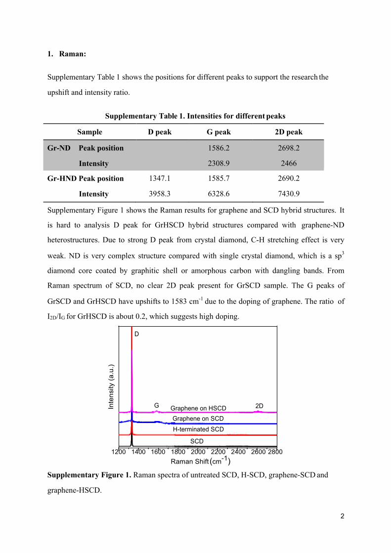
Supplementary Figure 1 shows the Raman results for graphene and SCD hybrid structures. It
is hard to analysis D peak for GrHSCD hybrid structures compared with graphene-ND
heterostructures. Due to strong D peak from crystal diamond, C-H stretching effect is very
weak. ND is very complex structure compared with single crystal diamond, which is a sp3
diamond core coated by graphitic shell or amorphous carbon with dangling bands. From
Raman spectrum of SCD, no clear 2D peak present for GrSCD sample. The G peaks of
GrSCD and GrHSCD have upshifts to 1583 cm-1 due to the doping of graphene. The ratio of
I2D/IG for GrHSCD is about 0.2, which suggests high doping.
1200 1400 1600 1800 2000 2200 2400 2600 2800 Raman Shift (cm-1)
Supplementary Figure 1. Raman spectra of untreated SCD, H-SCD, graphene-SCD and
graphene-HSCD.
Inte
nsity
(a.u
.)
3
�
2. XPS:
Supplementary Table 2 gives the intensity area for sp2 and sp3 peaks of two heterostructure
and calculate the hydrogen coverage.
Supplementary Table 2.Intensity area for sp2 and sp3 peaks
Sample sp2 sp3
θ θ/(1+θ)
Gr-ND 64137.23 14852.65 0.23 19%
Gr-HND 25508.2 15415.4 0.61 37%
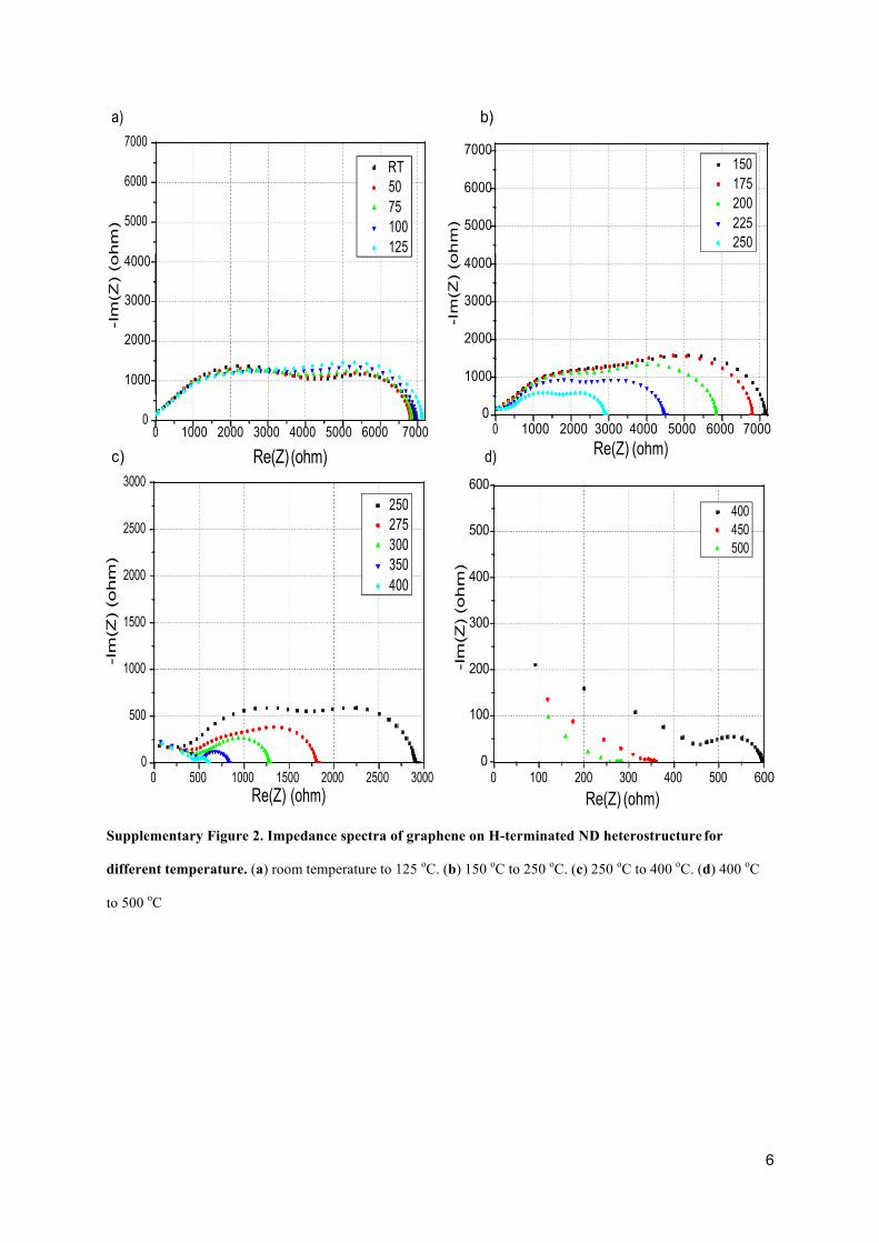
3. Impedance spectroscope for different temperatures:
Impedance spectroscopy is a useful tool for investigating the electric and dielectric behaviour
of electronic or mixed conductor ceramic materials1. This method involves measuring the
impedance as a function of frequency by applying a sinusoidal input voltage and measuring
the output current. The impedance Z as a function of angular frequency ω can be written in
the following complex form:
𝑍(𝜔) = 𝑍′(𝜔) + 𝑗𝑍′′(𝜔) (1) 𝑍′(𝜔) = ∑𝑛
𝑅 𝑖 (2) 𝑖=1 2 2
𝑍′′(𝜔) =
∑𝑛
1+𝜔2𝑅𝑖 𝐶𝑖
𝜔𝑅2𝐶
(3)
𝑖=1 2 2
1+𝜔2𝑅𝑖 𝐶𝑖
Where Z’(ω) is the real part of the impedance, associated to the resistive contribution of the
measured sample, whereas Z’’(ω) is the imaginary part of the impedance associated to the
capacitive contribution. The variable 𝑛 used in the summation can take integer values between 1 and 3, corresponding to the different type of conduction path2. By plotting the real
part against the imaginary part of the impedance as a function of frequency we get the so-
caller Cole-Cole plot. The Cole-Cole plot is a very using tool for determining the conduction
mechanism in the material by fitting an equivalent circuit2. The most dielectric simple
model consists of a resistor in series with a RC time constant which is associated to a

4
semicircle in the Cole-Cole plot.
5
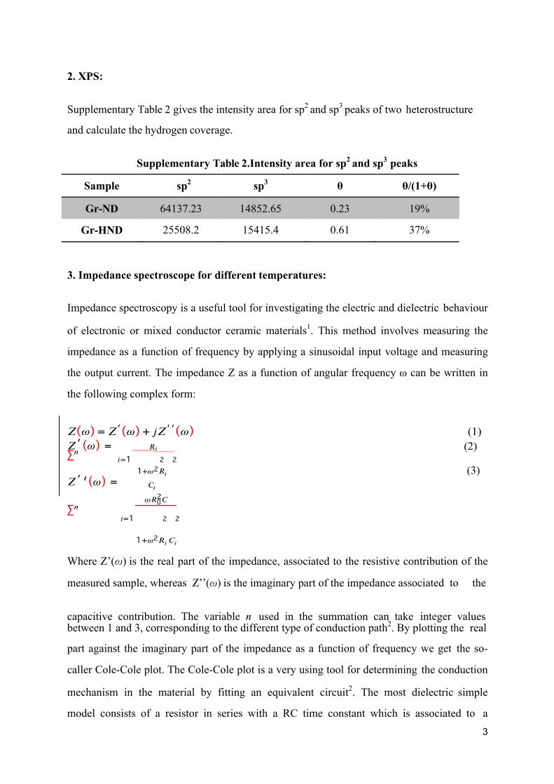
The graphene-H-terminated ND sample was analysed using an AC impedance analyser with
two Au/Ti (300 nm/10 nm) contacts at vacuum level. The frequency scale is from 0.1 Hz to
10 MHz. The measurement was taken from a range of temperature from room temperature to
500 oC. Increasing the temperature up to 125 oC, the results show that the radius for the low
frequency semicircle increases while the high frequency semicircle shows little change in
shape (Supplementary Fig. 2a). If we assign the low frequency semicircle to the graphene
surface conduction path, we would expect the conductivity to decrease owing to the
evaporation of the water layer on the surface.
At this temperature we would expect negligible modifications in the graphene-ND interface,
so the high frequency semicircle may be associated to this conduction path. At higher
temperatures from 150 oC to 250 oC both semicircles start to decrease. For the low frequency
semicircle this might be due to the elimination of residues or remaining PMMA on the
graphene surface, which would explain its increasing conductivity. Whereas for the high
frequency semicircle, this can be explained in terms of a possible activation of the hydrogen
bonds in the graphene-ND interface. Further increasing the temperature the high frequency
semicircle decreases at a higher rate than the other, and results show that after 275 oC we
have only one semicircle that further decreases up to 500 oC (Supplementary Fig.2c). The low
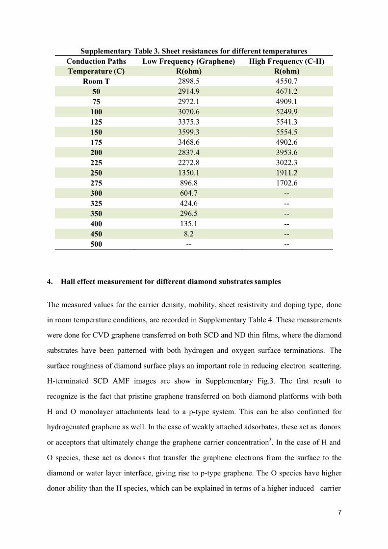
frequency semicircle after 400 oC is too small to show. The sheet resistances are given for the
two semicircles as the sample’s temperatures are increased in supplementary Table 3. At these
temperatures we would expect breaking of C-H bonds between the graphene-ND interface,
which would ultimately eliminate its associated conduction path leaving only the graphene
surface conduction path.
6
RT 50 75 100 125
150 175 200 225 250
250 275 300 350 400
-Im
(Z)
(oh
m)
-Im
(Z)
(oh
m)
a) b) 7000
6000
5000
7000
6000
5000
4000 4000
3000 3000
2000 2000
1000 1000
0 0 1000 2000 3000 4000 5000 6000 7000
0 0 1000 2000 3000 4000 5000 6000 7000
c) 3000
Re(Z) (ohm) d) 600
Re(Z) (ohm)
2500
2000
500
400
1500 300
1000 200
500 100
0 0 500 1000 1500 2000 2500 3000
Re(Z) (ohm)
0 0 100 200 300 400 500 600
Re(Z) (ohm)
Supplementary Figure 2. Impedance spectra of graphene on H-terminated ND heterostructure for
different temperature. (a) room temperature to 125 oC. (b) 150 oC to 250 oC. (c) 250 oC to 400 oC. (d) 400 oC
to 500 oC
400 450 500
-Im
(Z)
(oh
m)
-Im
(Z)
(oh
m)
7
Supplementary Table 3. Sheet resistances for different temperatures Conduction Paths Low Frequency (Graphene) High Frequency (C-H) Temperature (C) R(ohm) R(ohm)
Room T 2898.5 4550.7 50 2914.9 4671.2 75 2972.1 4909.1 100 3070.6 5249.9 125 3375.3 5541.3 150 3599.3 5554.5 175 3468.6 4902.6 200 2837.4 3953.6 225 2272.8 3022.3 250 1350.1 1911.2 275 896.8 1702.6 300 604.7 -- 325 424.6 -- 350 296.5 -- 400 135.1 -- 450 8.2 -- 500 -- --
4. Hall effect measurement for different diamond substrates samples
The measured values for the carrier density, mobility, sheet resistivity and doping type, done
in room temperature conditions, are recorded in Supplementary Table 4. These measurements
were done for CVD graphene transferred on both SCD and ND thin films, where the diamond
substrates have been patterned with both hydrogen and oxygen surface terminations. The
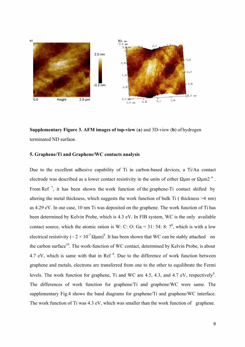
surface roughness of diamond surface plays an important role in reducing electron scattering.
H-terminated SCD AMF images are show in Supplementary Fig.3. The first result to
recognize is the fact that pristine graphene transferred on both diamond platforms with both
H and O monolayer attachments lead to a p-type system. This can be also confirmed for
hydrogenated graphene as well. In the case of weakly attached adsorbates, these act as donors
or acceptors that ultimately change the graphene carrier concentration3. In the case of H and
O species, these act as donors that transfer the graphene electrons from the surface to the
diamond or water layer interface, giving rise to p-type graphene. The O species have higher
donor ability than the H species, which can be explained in terms of a higher induced carrier
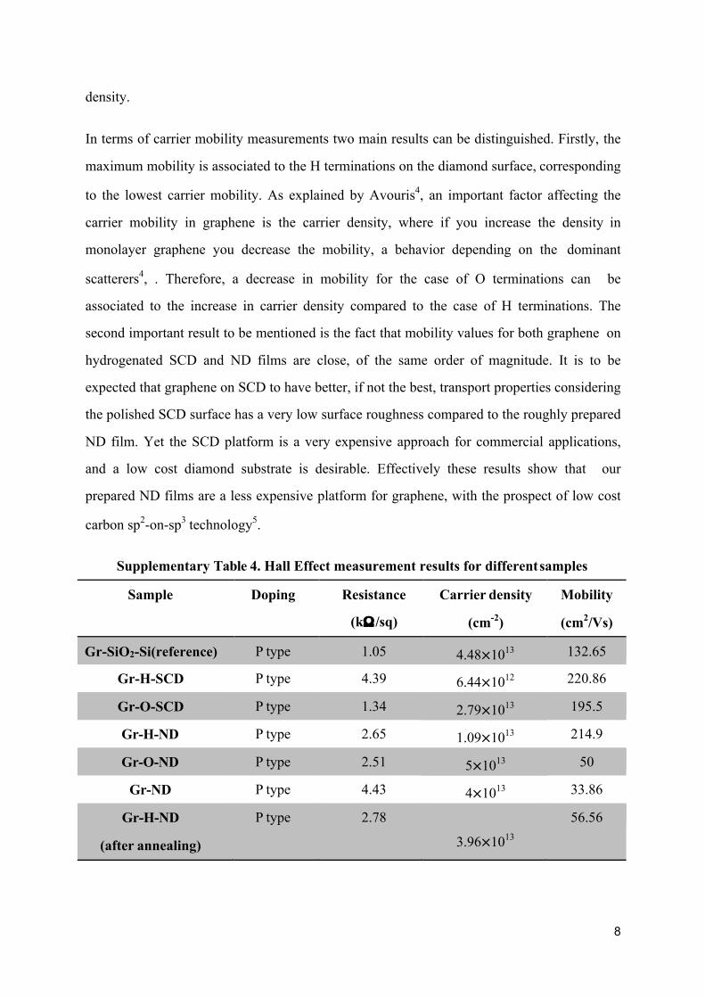
8
density.
In terms of carrier mobility measurements two main results can be distinguished. Firstly, the
maximum mobility is associated to the H terminations on the diamond surface, corresponding
to the lowest carrier mobility. As explained by Avouris4, an important factor affecting the
carrier mobility in graphene is the carrier density, where if you increase the density in
monolayer graphene you decrease the mobility, a behavior depending on the dominant
scatterers4, . Therefore, a decrease in mobility for the case of O terminations can be
associated to the increase in carrier density compared to the case of H terminations. The
second important result to be mentioned is the fact that mobility values for both graphene on
hydrogenated SCD and ND films are close, of the same order of magnitude. It is to be
expected that graphene on SCD to have better, if not the best, transport properties considering
the polished SCD surface has a very low surface roughness compared to the roughly prepared
ND film. Yet the SCD platform is a very expensive approach for commercial applications,
and a low cost diamond substrate is desirable. Effectively these results show that our
prepared ND films are a less expensive platform for graphene, with the prospect of low cost
carbon sp2-on-sp3 technology5.
Supplementary Table 4. Hall Effect measurement results for different samples
Sample Doping Resistance
(kΩ /sq)
Carrier density
(cm-2)
Mobility
(cm2/Vs)
Gr-SiO2-Si(reference) P type 1.05 4.48×10¹³ 132.65
Gr-H-SCD P type 4.39 6.44×10¹² 220.86
Gr-O-SCD P type 1.34 2.79×10¹³ 195.5
Gr-H-ND P type 2.65 1.09×10¹³ 214.9
Gr-O-ND P type 2.51 5×10¹³ 50
Gr-ND P type 4.43 4×10¹³ 33.86
Gr-H-ND
(after annealing)
P type 2.78
3.96×10¹³
56.56
9
a)
Supplementary Figure 3. AFM images of top-view (a) and 3D-view (b) of hydrogen
terminated ND surface.
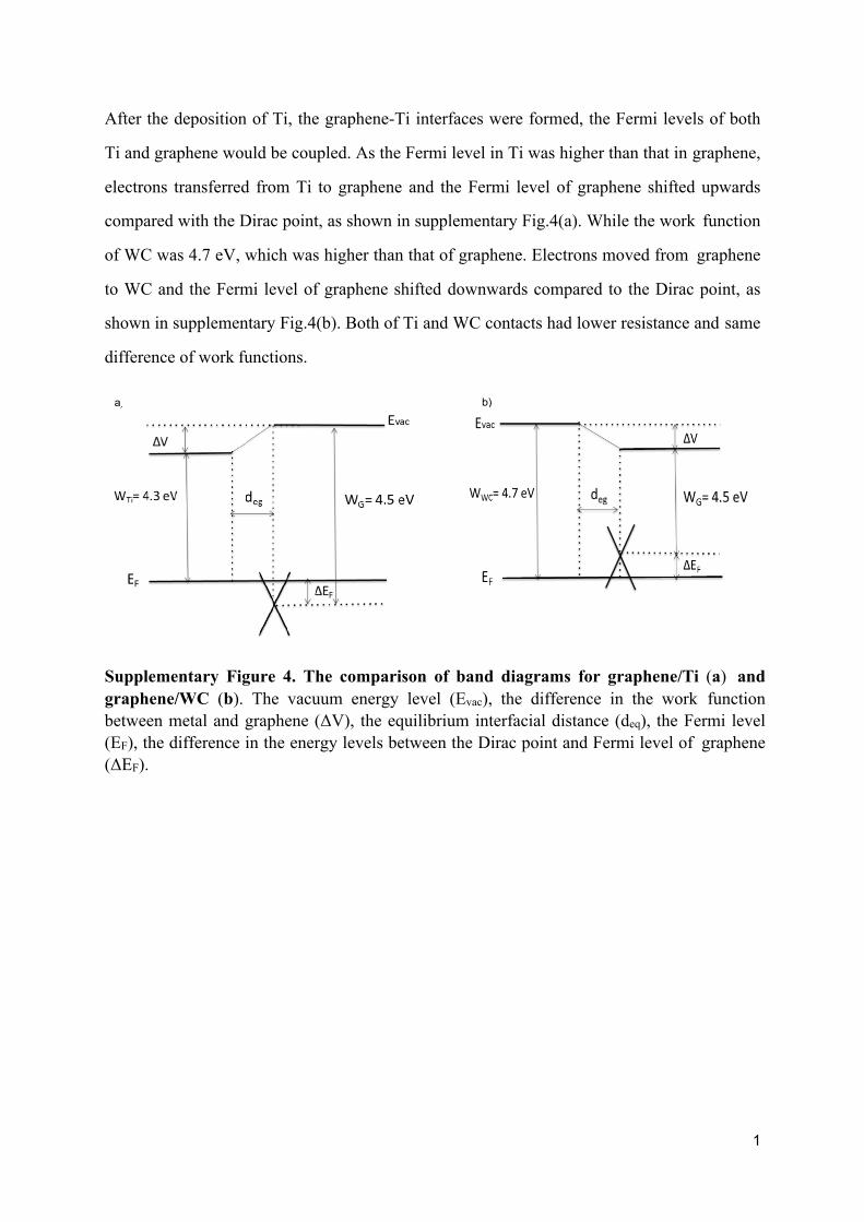
5. Graphene/Ti and Graphene/WC contacts analysis
Due to the excellent adhesive capability of Ti in carbon-based devices, a Ti/Au contact
electrode was described as a lower contact resistivity in the units of either Ωµm or Ωµm2 6 .
From Ref 7, it has been shown the work function of the graphene-Ti contact shifted by
altering the metal thickness, which suggests the work function of bulk Ti ( thickness >4 nm)
as 4.29 eV. In our case, 10 nm Ti was deposited on the graphene. The work function of Ti has
been determined by Kelvin Probe, which is 4.3 eV. In FIB system, WC is the only available
contact source, which the atomic ration is W: C: O: Ga = 31: 54: 8: 78, which is with a low
electrical resistivity (~ 2 × 10⁻⁷ Ωµm)9. It has been shown that WC can be stably attached on
the carbon surface10. The work-function of WC contact, determined by Kelvin Probe, is about
4.7 eV, which is same with that in Ref 8. Due to the difference of work function between
graphene and metals, electrons are transferred from one to the other to equilibrate the Fermi
levels. The work function for graphene, Ti and WC are 4.5, 4.3, and 4.7 eV, respectively6.
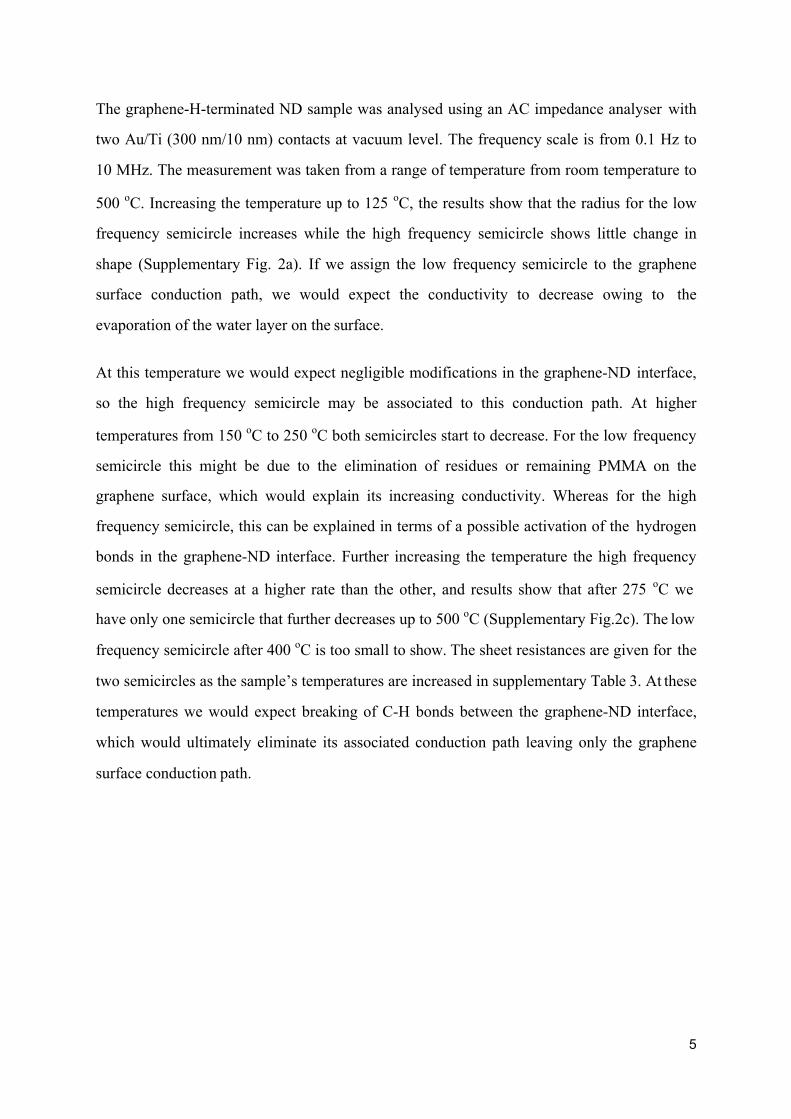
The differences of work function for graphene/Ti and graphene/WC were same. The
supplementary Fig.4 shows the band diagrams for graphene/Ti and graphene/WC interface.
The work function of Ti was 4.3 eV, which was smaller than the work function of graphene.
b)
10
After the deposition of Ti, the graphene-Ti interfaces were formed, the Fermi levels of both
Ti and graphene would be coupled. As the Fermi level in Ti was higher than that in graphene,
electrons transferred from Ti to graphene and the Fermi level of graphene shifted upwards
compared with the Dirac point, as shown in supplementary Fig.4(a). While the work function
of WC was 4.7 eV, which was higher than that of graphene. Electrons moved from graphene
to WC and the Fermi level of graphene shifted downwards compared to the Dirac point, as
shown in supplementary Fig.4(b). Both of Ti and WC contacts had lower resistance and same
difference of work functions.
b)
Supplementary Figure 4. The comparison of band diagrams for graphene/Ti (a) and graphene/WC (b). The vacuum energy level (Evac), the difference in the work function between metal and graphene (ΔV), the equilibrium interfacial distance (deq), the Fermi level (EF), the difference in the energy levels between the Dirac point and Fermi level of graphene (ΔEF).
a)
10
Reference:
1. Macdonald, J. Impedance spectroscopy: Models, data fitting, and analysis. Solid State Ionics, 176, 1961–1969, (2005).
2. Conway, B. E. in Impedance Spectroscopy: Theory, Experiment, and Applications, 2nd Edn. (eds Barsoukov E. & Macdonald J.R) Ch. 4, 475-477(John Wiley & Sons, 2005)
3. Zhao, F. et al. Electronic properties of graphene-single crystal diamond heterostructures. J. Appl. Phys.,
114, 053709, (2013).
4. Avouris, P. Graphene: Electronic and Photonic Properties and Devices. Nano Lett., 4285–4294,(2010).
5. Yu, J., Liu, G., Sumant, A. V, Goyal, V. & Balandin, A. a. Graphene-on-diamond devices with increased current-carrying capacity: carbon sp2-on-sp3 technology. Nano Lett., 12, 1603–8 (2012).
6. Nagashio, K. et al. Contact resistivity and current flow path at metal/graphene contact. Appl. Phys. Lett.
97, 143514 (2010).
7. Yang, S. et al. Direct obsercation of the work function evolution of graphene-two-dimensional metal
contacts. J. Mater. Chem. C, 2, 8042-6 (2014).
8. Kometani, R. and Ishhara, S. Nanoelectromechanical device fabrications by 3-D nanotechnology using
focused-ion beams. Sci. Tcchnol. Adv. Mater. 10, 034501 (2009).
9. Pierson, H. O. in Handbook of chemical vapor deposition: Principles, Technology, and Applications.
(eds Pierson, H. O.) Ch. 9, 253-254 (William Andrew Inc. 1999).
10. Chen, W. F.,et al.Tungsten Carbide-Nitride on Graphene Nanoplatelets as a Durable Hydrogen Evolution Electrocatalyst. ChemSusChem, 7, 2414–2418 (2014).