gpu 2000r “w”, “v”, or “t” modbus/modbus plus ... · departs from the standard type of...
TRANSCRIPT
GPU 2000R “W”, “V”, or “T” Modbus/Modbus Plus Automation Technical Guide
1
Section 1 - Introduction
With the introduction of a microprocessor based protective relay, today’s relay protection engineer must befamiliar with topics outside of traditional relaying schemes. It is intended that the production of this manual willenable the relay engineer to understand the principles of a microprocessor-based relay’s inclusion in a substationautomation project.
Substation automation is heavily dependent upon integration of the appropriate components to allow reporting ofmetering and event data. The foundation of a successful automation solution is thorough engineering of acommunication system. The Generation Protection Unit (GPU) is the culmination of intensive design efforts andrelaying experience, which combine protective relaying and communication capabilities at an economical price.Through the evolution of protective relays, it was decided that a special manual needed to serve today’s powerautomation specialist.
This manual is intended to give the reader an in-depth explanation of the communication interfaces available withthe Generator Protection Unit. Successful integration of microprocessor based relays like the GPU depends onnot just understanding the bits and bytes of a particular protocol. It is the inherent understanding and applicationof such esoteric topics as physical interfaces, real time control, manufacturer independent device integration,throughput vs. speed of communication, … which influences the success of an automation project.
In many cases the individual performing the SCADA integration is not a relay protection engineer. This manualdeparts from the standard type of relay manual in that each data type is explained and each bit, byte and wordmeaning is explained. Several application examples are given within each section. A description of each protocolcommand is illustrated for the benefit of the user. Appendices are included detailing application notes, whichaugment the text. An explanation of the product’s physical interfaces and the connectivity required is explored indepth. Explanations of register’s uses to increase overall throughput are also explored. Throughput is always anissue when the system is commissioned. Understanding ways to improve the system data update is explained.
Several steps are required to permit successful communication between devices:
1. Identification of the hardware components (Section 2).
2. Correct physical connection between devices (Section 3).
3. Correct device configuration of port protocol and operation parameters (Section 4).
4. Generation and interpretation of the protocol command strings (Section 5).
The following sections shall explore the following procedures in depth when establishing a communicationautomation system, utilizing the GPU 2000R. An additional Section (Section 6) illustrates troubleshooting andcommissioning of the Modbus/Modbus Plus Networks.
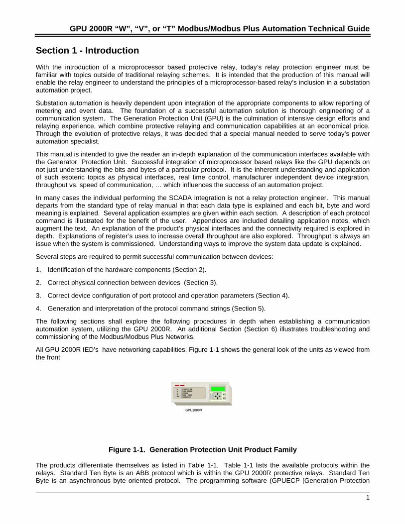
All GPU 2000R IED’s have networking capabilities. Figure 1-1 shows the general look of the units as viewed fromthe front
E
C
ABCNRST
XX XXXXX XXXX XX XXXXXXXXXXX XXXX XXXXX XXXXXXX
STATUS TARGETS
GPU2000R
Figure 1-1. Generation Protection Unit Product Family
The products differentiate themselves as listed in Table 1-1. Table 1-1 lists the available protocols within therelays. Standard Ten Byte is an ABB protocol which is within the GPU 2000R protective relays. Standard TenByte is an asynchronous byte oriented protocol. The programming software (GPUECP [Generation Protection
GPU 2000R “W”, “V”, or “T” Modbus/Modbus Plus Automation Technical Guide
2
Unit External Communication Program]) allows configuration of the relay through a port on the units. StandardTen Byte is available through an RS232 or RS485 port on the GPU. It is very important to recognize that thereare two GPUECP programs to configure the IED. One GPU ECP program paratmerizes and configures the GPU2000R whereas another GPU ECP program parameterizes and configures the GPU 2000R “W” or GPU 2000R“V” or GPU 2000R “T” devices. It is important to recognize and identify the GPU 2000R device so that propercommunication and configuration may occur. Many individuals using the GPU will identify the device as aGPU2000R, when in reality, this may not be the case.
INCOM is an ABB protocol, which is a derivative of Standard Ten Byte. It is a modulated synchronous bit streamusing the same commands as in the Standard Ten Byte protocol. INCOM is available as an option for the GPU2000R relays as indicated within Table 1-1. Its physical interface is proprietary in that the GPU node expects amodulated signal.
Modbus is an industrial de-facto standard protocol, which has been widely embraced by the utility industry.Modbus has two emulation’s, RTU, which is a synchronous protocol and ASCII which is an asynchronousprotocol. Modbus uses only one command set, but two emulation’s. Modbus strengths are that it uses astandard RS232 or RS485 interface to interconnect nodes on a network.
Modbus Plus is a hybrid protocol refinement of Modbus. Modbus Plus has a proprietary physical interface whichis available to device manufacturers through a connectivity program with Groupe Schneider. The interface offersgreater speed and communication features than Modbus. Modbus Plus is only available on GPU 2000R Models“W”, “V”, or “T”. It is not available on the “R” versions of the product. It should be noted that the Modbus/ModbusPlus memory maps differ between the “R” models and the W/V/T models. Within this document, only the GPU2000R “W”, “V”, and “T” devices are covered. The memory mapping for the GPU 2000R “R” models are notdescribed within this automation manual.
Table 1-1. Protocol Capabilities Listed by Product Type
PRODUCT PROTOCOL NOTESGPU 2000R “R” Standard Ten Byte Addressable Front Com, Com 1 and Aux Com
INCOM 2 Wire (and Shield) Current Injection Physical InterfaceGPU 2000R “R”Modbus RS232 or RS485
GPU 2000R “R” Standard Ten Byte RS232 or RS485INCOM 2 Wire (and Shield) Current Injection Physical InterfaceModbus RS232 or RS485
GPU 2000R“W”, “V” or “T”
Modbus Plus Proprietary Current Injection Physical Interface
Within this document, only Modbus, and Modbus Plus protocols shall be covered in depth. Standard 10 Byte,and INCOM shall be explained superficially. If one would need to reference the specific details of Standard TenByte or INCOM protocols, please reference the engineering specifications concerning these topics in Appendix Aof this document.
GPU 2000R “W”, “V”, or “T” Modbus/Modbus Plus Automation Technical Guide
3
Section 2 - Communication Card Identification and Physical PortCharacteristics
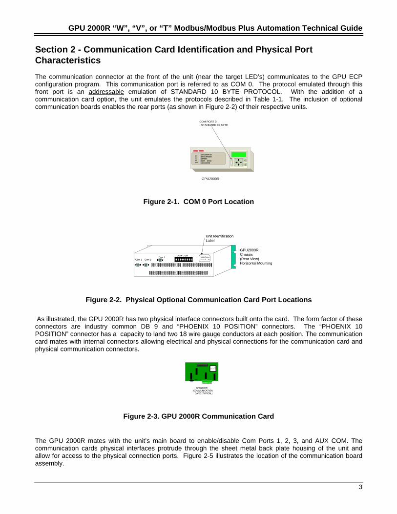
The communication connector at the front of the unit (near the target LED’s) communicates to the GPU ECPconfiguration program. This communication port is referred to as COM 0. The protocol emulated through thisfront port is an addressable emulation of STANDARD 10 BYTE PROTOCOL. With the addition of acommunication card option, the unit emulates the protocols described in Table 1-1. The inclusion of optionalcommunication boards enables the rear ports (as shown in Figure 2-2) of their respective units.
E
C
ABCNRST
XX XXXXX XXXX XX XXXXXXXXXXX XXXX XXXXX XXXXXXX
STATUS TARGETS
GPU2000R
COM PORT 0- STANDARD 10 BYTE
Figure 2-1. COM 0 Port Location
Com 3Com 1 Com 2
AUX COM
GPU2000RChassis(Rear View)Horizontal Mounting
Model xxxxct xx pt xx
Unit Identification Label
Figure 2-2. Physical Optional Communication Card Port Locations
As illustrated, the GPU 2000R has two physical interface connectors built onto the card. The form factor of theseconnectors are industry common DB 9 and “PHOENIX 10 POSITION” connectors. The “PHOENIX 10POSITION” connector has a capacity to land two 18 wire gauge conductors at each position. The communicationcard mates with internal connectors allowing electrical and physical connections for the communication card andphysical communication connectors.
AUX/COM3.0
12345
GPU2000R COMMUNICATION CARD (TYPICAL)
Figure 2-3. GPU 2000R Communication Card
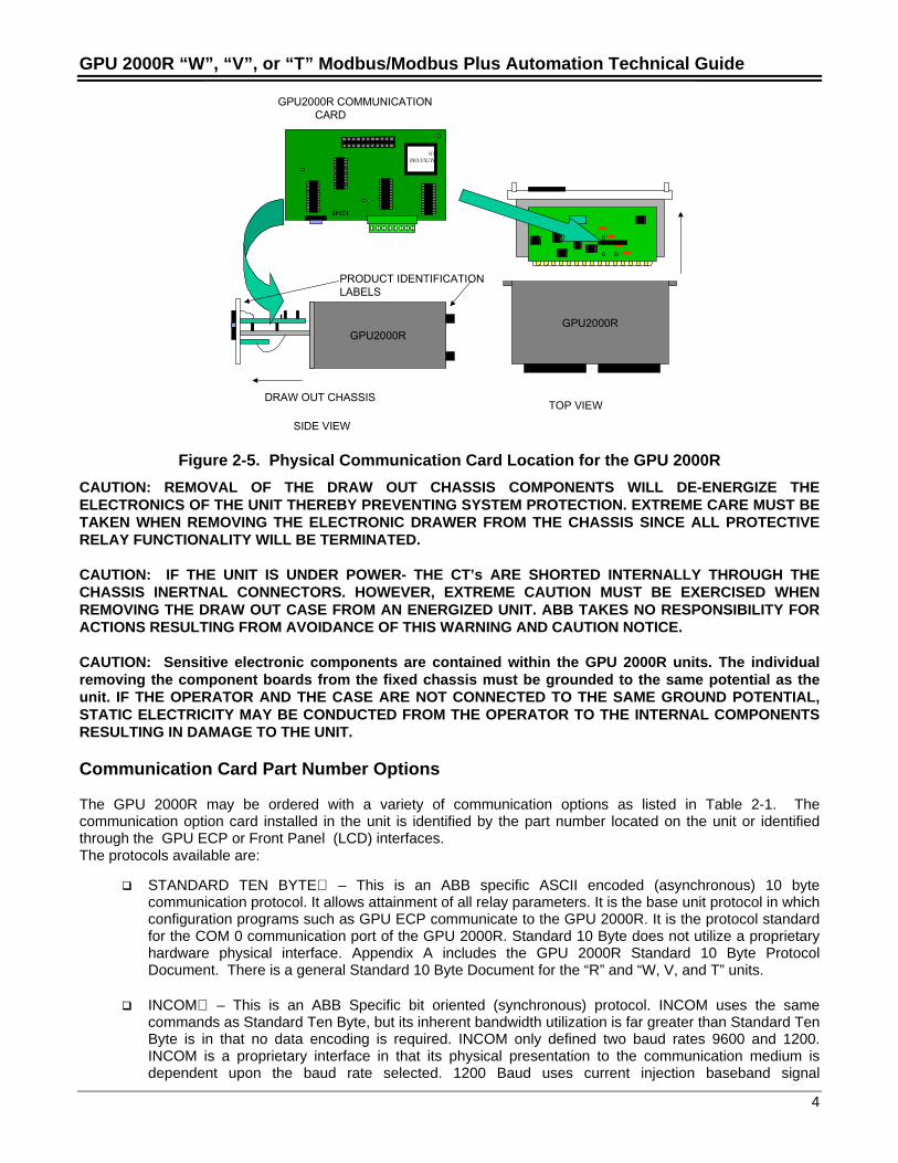
The GPU 2000R mates with the unit’s main board to enable/disable Com Ports 1, 2, 3, and AUX COM. Thecommunication cards physical interfaces protrude through the sheet metal back plate housing of the unit andallow for access to the physical connection ports. Figure 2-5 illustrates the location of the communication boardassembly.
GPU 2000R “W”, “V”, or “T” Modbus/Modbus Plus Automation Technical Guide
4
GPU2000R COMMUNICATION CARD
GPU2000R
DRAW OUT CHASSIS
PRODUCT IDENTIFICATIONLABELS
AUX/COM3.0
12345
SIDE VIEW
GPU2000R
TOP VIEW
Figure 2-5. Physical Communication Card Location for the GPU 2000R
CAUTION: REMOVAL OF THE DRAW OUT CHASSIS COMPONENTS WILL DE-ENERGIZE THEELECTRONICS OF THE UNIT THEREBY PREVENTING SYSTEM PROTECTION. EXTREME CARE MUST BETAKEN WHEN REMOVING THE ELECTRONIC DRAWER FROM THE CHASSIS SINCE ALL PROTECTIVERELAY FUNCTIONALITY WILL BE TERMINATED.
CAUTION: IF THE UNIT IS UNDER POWER- THE CT’s ARE SHORTED INTERNALLY THROUGH THECHASSIS INERTNAL CONNECTORS. HOWEVER, EXTREME CAUTION MUST BE EXERCISED WHENREMOVING THE DRAW OUT CASE FROM AN ENERGIZED UNIT. ABB TAKES NO RESPONSIBILITY FORACTIONS RESULTING FROM AVOIDANCE OF THIS WARNING AND CAUTION NOTICE.
CAUTION: Sensitive electronic components are contained within the GPU 2000R units. The individualremoving the component boards from the fixed chassis must be grounded to the same potential as theunit. IF THE OPERATOR AND THE CASE ARE NOT CONNECTED TO THE SAME GROUND POTENTIAL,STATIC ELECTRICITY MAY BE CONDUCTED FROM THE OPERATOR TO THE INTERNAL COMPONENTSRESULTING IN DAMAGE TO THE UNIT.
Communication Card Part Number Options
The GPU 2000R may be ordered with a variety of communication options as listed in Table 2-1. Thecommunication option card installed in the unit is identified by the part number located on the unit or identifiedthrough the GPU ECP or Front Panel (LCD) interfaces.The protocols available are:
STANDARD TEN BYTE – This is an ABB specific ASCII encoded (asynchronous) 10 bytecommunication protocol. It allows attainment of all relay parameters. It is the base unit protocol in whichconfiguration programs such as GPU ECP communicate to the GPU 2000R. It is the protocol standardfor the COM 0 communication port of the GPU 2000R. Standard 10 Byte does not utilize a proprietaryhardware physical interface. Appendix A includes the GPU 2000R Standard 10 Byte ProtocolDocument. There is a general Standard 10 Byte Document for the “R” and “W, V, and T” units.
INCOM – This is an ABB Specific bit oriented (synchronous) protocol. INCOM uses the samecommands as Standard Ten Byte, but its inherent bandwidth utilization is far greater than Standard TenByte is in that no data encoding is required. INCOM only defined two baud rates 9600 and 1200.INCOM is a proprietary interface in that its physical presentation to the communication medium isdependent upon the baud rate selected. 1200 Baud uses current injection baseband signal
GPU 2000R “W”, “V”, or “T” Modbus/Modbus Plus Automation Technical Guide
5
presentation, whereas 9600-Baud implements a phase shift frequency in its representation of digital 1and 0 values. Appendix A includes the GPU 2000R Standard Ten Byte Protocol document whichdescribes INCOM in further detail.
MODBUS – This is an Industrial standard. The protocol allows a single master device tocommunicate with several slave devices. It has gained wide acceptance in that a great majority of utilitydevices incorporate Modbus protocol. Modbus Protocol is physical interface independent. ModbusProtocol has two emulation’s RTU (a synchronous bit oriented emulation) and ASCII (an asynchronousbyte oriented emulation). The GPU 2000R may be configured for both emulations. The discussion ofModbus protocol is included in this document. Please reference the GPU 2000R Modbus/Modbus PlusAutomation Technical Guide TG 7.11.1.7-71 for a discussion of this protocol.
MODBUS PLUS – This protocol is also and industrial standard. Modbus Plus allows up to 64 devicesto communicate on a single network using token passing techniques. 5 networks may be bridged(interconnected) to form a larger Modbus Plus network. The Modbus Plus protocol is fast (1 megabaud)and uses several advanced techniques to maximize bandwidth. The physical interface to Modbus Plusis proprietary and regulated by Groupe Schneider. Modbus Plus is the incorporation of Modbuscommands on a HDLC - like protocol using a current injection interface. The discussion of ModbusPlus protocol is included in this document. Only the GPU 2000R “W”, ”V”, or “T” has the capability ofcommunicating using the Modbus Plus protocol. Please reference the GPU 2000R Modbus/ModbusPlus Automation Technical Guide TG 7.11.1.7-71 for a discussion of this protocol. (AVAILABLE ONTHE GPU 2000R MODELS “W”, “V”, and “T” ONLY).
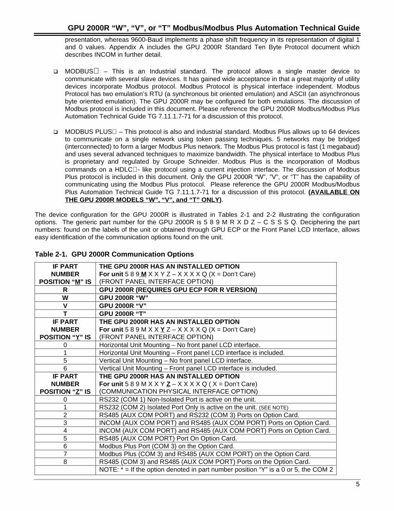
The device configuration for the GPU 2000R is illustrated in Tables 2-1 and 2-2 illustrating the configurationoptions. The generic part number for the GPU 2000R is 5 8 9 M R X D Z – C S S S Q. Deciphering the partnumbers: found on the labels of the unit or obtained through GPU ECP or the Front Panel LCD Interface, allowseasy identification of the communication options found on the unit.
Table 2-1. GPU 2000R Communication Options
IF PARTNUMBER
POSITION “M” IS
THE GPU 2000R HAS AN INSTALLED OPTIONFor unit 5 8 9 M X X Y Z – X X X X Q (X = Don’t Care)(FRONT PANEL INTERFACE OPTION)
R GPU 2000R (REQUIRES GPU ECP FOR R VERSION)W GPU 2000R “W”V GPU 2000R “V”T GPU 2000R “T”
IF PARTNUMBER
POSITION “Y” IS
THE GPU 2000R HAS AN INSTALLED OPTIONFor unit 5 8 9 M X X Y Z – X X X X Q (X = Don’t Care)(FRONT PANEL INTERFACE OPTION)
0 Horizontal Unit Mounting – No front panel LCD interface.1 Horizontal Unit Mounting – Front panel LCD interface is included.5 Vertical Unit Mounting – No front panel LCD interface.6 Vertical Unit Mounting – Front panel LCD interface is included.
IF PARTNUMBER
POSITION “Z” IS
THE GPU 2000R HAS AN INSTALLED OPTIONFor unit 5 8 9 M X X Y Z – X X X X Q ( X = Don’t Care)(COMMUNICATION PHYSICAL INTERFACE OPTION)
0 RS232 (COM 1) Non-Isolated Port is active on the unit.1 RS232 (COM 2) Isolated Port Only is active on the unit. (SEE NOTE)
2 RS485 (AUX COM PORT) and RS232 (COM 3) Ports on Option Card.3 INCOM (AUX COM PORT) and RS485 (AUX COM PORT) Ports on Option Card.4 INCOM (AUX COM PORT) and RS485 (AUX COM PORT) Ports on Option Card.5 RS485 (AUX COM PORT) Port On Option Card.6 Modbus Plus Port (COM 3) on the Option Card.7 Modbus Plus (COM 3) and RS485 (AUX COM PORT) on the Option Card.8 RS485 (COM 3) and RS485 (AUX COM PORT) Ports on the Option Card.
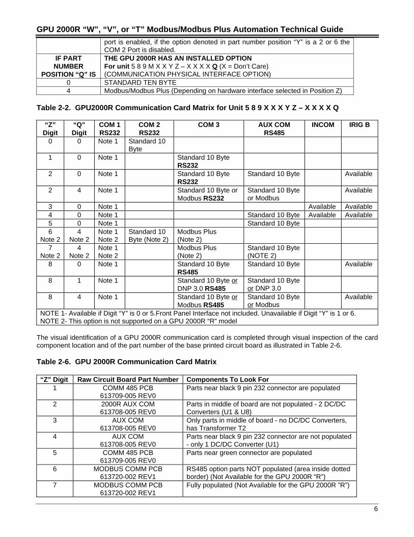
NOTE: * = If the option denoted in part number position “Y” is a 0 or 5, the COM 2
GPU 2000R “W”, “V”, or “T” Modbus/Modbus Plus Automation Technical Guide
6
port is enabled, if the option denoted in part number position “Y” is a 2 or 6 theCOM 2 Port is disabled.
IF PARTNUMBER
POSITION “Q” IS
THE GPU 2000R HAS AN INSTALLED OPTIONFor unit 5 8 9 M X X Y Z – X X X X Q (X = Don’t Care)(COMMUNICATION PHYSICAL INTERFACE OPTION)
0 STANDARD TEN BYTE4 Modbus/Modbus Plus (Depending on hardware interface selected in Position Z)
Table 2-2. GPU2000R Communication Card Matrix for Unit 5 8 9 X X X Y Z – X X X X Q
“Z”Digit
“Q”Digit
COM 1RS232
COM 2RS232
COM 3 AUX COMRS485
INCOM IRIG B
0 0 Note 1 Standard 10Byte
1 0 Note 1 Standard 10 ByteRS232
2 0 Note 1 Standard 10 ByteRS232
Standard 10 Byte Available
2 4 Note 1 Standard 10 Byte orModbus RS232
Standard 10 Byteor Modbus
Available
3 0 Note 1 Available Available4 0 Note 1 Standard 10 Byte Available Available5 0 Note 1 Standard 10 Byte6
Note 24
Note 2Note 1Note 2
Standard 10Byte (Note 2)
Modbus Plus(Note 2)
7Note 2
4Note 2
Note 1Note 2
Modbus Plus(Note 2)
Standard 10 Byte(NOTE 2)
8 0 Note 1 Standard 10 ByteRS485
Standard 10 Byte Available
8 1 Note 1 Standard 10 Byte orDNP 3.0 RS485
Standard 10 Byteor DNP 3.0
8 4 Note 1 Standard 10 Byte orModbus RS485
Standard 10 Byteor Modbus
Available
NOTE 1- Available if Digit “Y” is 0 or 5.Front Panel Interface not included. Unavailable if Digit “Y” is 1 or 6.NOTE 2- This option is not supported on a GPU 2000R “R” model
The visual identification of a GPU 2000R communication card is completed through visual inspection of the cardcomponent location and of the part number of the base printed circuit board as illustrated in Table 2-6.
Table 2-6. GPU 2000R Communication Card Matrix
“Z” Digit Raw Circuit Board Part Number Components To Look For1 COMM 485 PCB
613709-005 REV0Parts near black 9 pin 232 connector are populated
2 2000R AUX COM613708-005 REV0
Parts in middle of board are not populated - 2 DC/DCConverters (U1 & U8)
3 AUX COM613708-005 REV0
Only parts in middle of board - no DC/DC Converters,has Transformer T2
4 AUX COM613708-005 REV0
Parts near black 9 pin 232 connector are not populated- only 1 DC/DC Converter (U1)
5 COMM 485 PCB613709-005 REV0
Parts near green connector are populated
6 MODBUS COMM PCB613720-002 REV1
RS485 option parts NOT populated (area inside dottedborder) (Not Available for the GPU 2000R “R”)
7 MODBUS COMM PCB613720-002 REV1
Fully populated (Not Available for the GPU 2000R ”R”)
GPU 2000R “W”, “V”, or “T” Modbus/Modbus Plus Automation Technical Guide
7
8 AUX & AUX613755-002 REV0
Fully populated
Unit Communication Card Verification
There are several ways to identify the communication cards inserted in the GPU 2000R units. Some of themethods require the unit to be powered up. Other methods require the unit to be taken out of service.
To identify the unit part number of the present GPU 2000R, the following steps may be executed to facilitate unitidentification.
1. With the unit energized, if the unit has a Front Panel LCD (Refer to Tables 2-1 through 2-4 inclusive foridentification) Interface:
1. Depress the “E” Key.2. Depress the Arrow Down Key “↓ ” once to highlight the SETTINGS field. Depress the “E” Key.3. Depress the Arrow Down Key “↓ ” twice to highlight the UNIT INFORMATION field. Depress the “E” key.4. The Serial Number and Catalog Number shall be displayed.
If the Unit does not have a Front Panel LCD Interface (Refer to Tables 2-1 through 2-4 inclusive for identification)and the user has GPU ECP or if the user wishes not to use the unit’s Front Panel Interface:
1. Start GPU ECP.2. Depress the “DIRECT ACCESS” selection button presented in the pop-up window.3. Depress the “CONNECT” option selection presented within the pop-up window.4. Select the “HELP” Menu option at the top right-hand section of the menu bar.5. Select the Drag-Down Menu item “UNIT INFORMATION”.6. A pop-up window shall appear with the Serial Number and Catalog Number.
2. At the back of the GPU 2000R, chassis, in the left-hand lower section of the unit, a label shall appearindicating the serial number and model number of the unit. It should match the data presented in the GPUECP, or Front Panel Interface (FPI) Menus. If it does not, please contact the factory.
3. As a final check, if the GPU 2000R, can be powered-down or if protection can be interrupted, loosen the frontpanel screws at the front of the unit. Remove the product component drawer from the chassis. Face the frontpanel interface, and rotate the board so that the semiconductor components are directly visible. On thebackside of the metal panel supporting the Front Panel Interface, a label shall be available indicating theserial number and model number. These numbers should match those obtained in steps 1 and 2. If they donot, please contact the factory.
GPU 2000R “W”, “V”, or “T” Modbus/Modbus Plus Automation Technical Guide
8
Section 3 – GPU 2000R Device Connectivity
Communication between devices is only possible through connectivity of the units through a physical mediainterface. There are two or a maximum of three physical interface types on a GPU 2000R “R”, “W”, “V”, or “T” (RS232, RS 485 or Modbus Plus/INCOM). Table 3-1 lists the characteristics for each of the port types. Thosephysical interfaces are:
RS232 (isolated and non-isolated) RS485 (isolated)
Table 3-1. Physical Interface Options
GPU 2000R NotesCOM 0 RS232 Non Isolated Front Port Standard 10 ByteCOM 1 RS232 Non Isolated Standard 10 Byte OnlyCOM 2 RS232 Non Isolated Standard 10 Byte OnlyCOM 3 RS232 Isolated/RS485
Isolated or Modbus PlusGPU 2000R – Communication Option CardDetermines Physical Interface
AUX COM RS485 (Isolated) and/orINCOM
Physical Interface Dependent on CommunicationOption Card Interface Selected
RS232 Interface Connectivity
RS232 is perhaps the most utilized and least understood communication interface in use. RS232 is sometimesmisinterpreted to be a protocol; it is in fact a physical interface. A physical interface is the hardware and networkphysical media used to propagate a signal between devices. Examples of physical interfaces are RS232 seriallink, printer parallel port, current loop, V. 24, IEEE Bus… Examples of network media are, twisted copper pair,coaxial cable, free air…
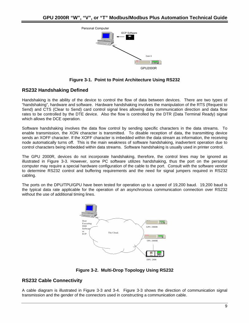
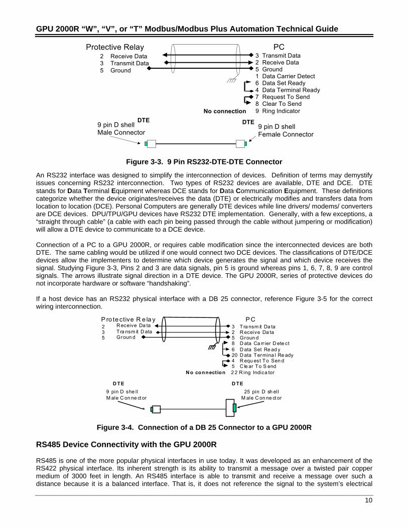
RS232 gained widespread acceptance due to its ability to connect to another RS232 device or modem. A modemis a device, which takes a communication signal and modulates it into another form. Common forms of modemsinclude telephone, fiber optic, microwave, and radio frequency. Modem connectivity allows attachment of multipledevices on a communication network or allows extension of communication distances in a network with twonodes. Physical connection of two devices or more than two devices require differing approaches. Figure 3-1illustrates a topology using two devices (point to point topology). Figure 3-2 illustrates a multi-drop topologybetween many nodes. RS232 was designed to allow two devices to communicate without using intermediatedevices.
Port Isolation
Network installation within a substation requires special considerations. A substation environment is harsh in thathigh levels of electromagnetic interference are present. Additional ground currents are present in suchinstallations. RS232 is an unbalanced network in that all signals are referenced to a common ground. On longercable runs, the potential of the signals at the sending device can be significantly lower than at the receiving enddue to electrical interference and induced ground current. This increases with long runs of cable and use ofunshielded cable. ABB Substation Automation and Protection recommends the length of RS232 cable be lessthan 10 feet (3 meters) for an un-isolated port and that the cable be shielded. Internal to a typical device, theRS232 transceivers are referenced to the electronic components internal ground. Any electrical interferencecould be coupled through the chip set and fed back to the device. Typical isolation ratings of a non-isolated portcould be as low as 1 volt. Such a port could allow electrical feedback of noise to the electronics for any signalinterference over 1 volt.
Coms 0 through 2 on DPU/TPU/GPU units are non–isolated. However an RS232 implementation on Com 3 usesopto-isolation technology which increases electrical isolation from the port to the devices internal circuitry to 2.3kV. It is highly desirable to utilize this port in connection to devices in longer cable runs and dedicatedcommunication networks. RS232 isolated ports are limited in connection distance for a maximum of fifty feet.
GPU 2000R “W”, “V”, or “T” Modbus/Modbus Plus Automation Technical Guide
9
EC
GPU2000R
Personal ComputerECP Software
Com 0
Figure 3-1. Point to Point Architecture Using RS232
RS232 Handshaking Defined
Handshaking is the ability of the device to control the flow of data between devices. There are two types of“handshaking”, hardware and software. Hardware handshaking involves the manipulation of the RTS (Request toSend) and CTS (Clear to Send) card control signal lines allowing data communication direction and data flowrates to be controlled by the DTE device. Also the flow is controlled by the DTR (Data Terminal Ready) signalwhich allows the DCE operation.
Software handshaking involves the data flow control by sending specific characters in the data streams. Toenable transmission, the XON character is transmitted. To disable reception of data, the transmitting devicesends an XOFF character. If the XOFF character is imbedded within the data stream as information, the receivingnode automatically turns off. This is the main weakness of software handshaking, inadvertent operation due tocontrol characters being imbedded within data streams. Software handshaking is usually used in printer control.
The GPU 2000R, devices do not incorporate handshaking, therefore, the control lines may be ignored asillustrated in Figure 3-3. However, some PC software utilizes handshaking, thus the port on the personalcomputer may require a special hardware configuration of the cable to the port. Consult with the software vendorto determine RS232 control and buffering requirements and the need for signal jumpers required in RS232cabling.
The ports on the DPU/TPU/GPU have been tested for operation up to a speed of 19,200 baud. 19,200 baud isthe typical data rate applicable for the operation of an asynchronous communication connection over RS232without the use of additional timing lines.
Host ExecutingHMI Softwareor ECP
DPU 2000
EC
EC
GPU 2000R
The Cloud.
TPU 2000R
STATUS
CC EE
Figure 3-2. Multi-Drop Topology Using RS232
RS232 Cable Connectivity
A cable diagram is illustrated in Figure 3-3 and 3-4. Figure 3-3 shows the direction of communication signaltransmission and the gender of the connectors used in constructing a communication cable.
GPU 2000R “W”, “V”, or “T” Modbus/Modbus Plus Automation Technical Guide
10
Protective Relay PC2 Receive Data 3 Transmit Data3 Transmit Data 2 Receive Data5 Ground 5 Ground
1 Data Carrier Detect6 Data Set Ready
4 Data Terminal Ready7 Request To Send8 Clear To Send
No connection 9 Ring Indicator
9 pin D shellMale Connector
9 pin D shellFemale Connector
DTE DTE
Figure 3-3. 9 Pin RS232-DTE-DTE Connector
An RS232 interface was designed to simplify the interconnection of devices. Definition of terms may demystifyissues concerning RS232 interconnection. Two types of RS232 devices are available, DTE and DCE. DTEstands for Data Terminal Equipment whereas DCE stands for Data Communication Equipment. These definitionscategorize whether the device originates/receives the data (DTE) or electrically modifies and transfers data fromlocation to location (DCE). Personal Computers are generally DTE devices while line drivers/ modems/ convertersare DCE devices. DPU/TPU/GPU devices have RS232 DTE implementation. Generally, with a few exceptions, a“straight through cable” (a cable with each pin being passed through the cable without jumpering or modification)will allow a DTE device to communicate to a DCE device.
Connection of a PC to a GPU 2000R, or requires cable modification since the interconnected devices are bothDTE. The same cabling would be utilized if one would connect two DCE devices. The classifications of DTE/DCEdevices allow the implementers to determine which device generates the signal and which device receives thesignal. Studying Figure 3-3, Pins 2 and 3 are data signals, pin 5 is ground whereas pins 1, 6, 7, 8, 9 are controlsignals. The arrows illustrate signal direction in a DTE device. The GPU 2000R, series of protective devices donot incorporate hardware or software “handshaking”.
If a host device has an RS232 physical interface with a DB 25 connector, reference Figure 3-5 for the correctwiring interconnection.
P ro te ctive R e la y P C2 R eceive Da ta 3 T ra nsm it Da ta3 Tra nsm it D ata 2 R eceive Da ta5 Groun d 5 Groun d
8 D ata Ca rr ier D ete ct6 D ata Set Re ad y
20 D ata Termina l Re ady4 R equ est To Sen d5 C le ar To S end
N o connection 2 2 R ing Indica tor
9 pin D she llM ale C on ne ct or
25 pin D sh ellM ale C on ne ct or
D TE D TE
Figure 3-4. Connection of a DB 25 Connector to a GPU 2000R
RS485 Device Connectivity with the GPU 2000R
RS485 is one of the more popular physical interfaces in use today. It was developed as an enhancement of theRS422 physical interface. Its inherent strength is its ability to transmit a message over a twisted pair coppermedium of 3000 feet in length. An RS485 interface is able to transmit and receive a message over such adistance because it is a balanced interface. That is, it does not reference the signal to the system’s electrical
GPU 2000R “W”, “V”, or “T” Modbus/Modbus Plus Automation Technical Guide
11
ground, as is the case in an RS232 interface. RS485 references the communication voltage levels to a pair ofwires isolated from system ground. Depending on the manufacturer’s implementation, isolation may be optical orelectronic. RS485 has two variants, two wires and four-wire. In the two-wire format, communication occurs overone single wire pair. In four-wire format, communication occurs over two wire pairs, transmit and receive. Thetwo-wire format is the most common in use. The GPU 2000R, supports half duplex two-wire format only. TheRS485 port is also optically isolated to provide for 3000 V of isolation.
The RS485 network supported and recommended by ABB requires the use of three conductor shielded cable.Suggested RS485 cable and the respective manufacturer’s wire numbers are:
• ALPHA 58902• Belden 9729• Belden 9829• Carol 58902
ABB does not support deviations from the specified cables. The selected cable types listed are of the type whichhave the appropriate physical and electrical characteristics for installation in substation environments.
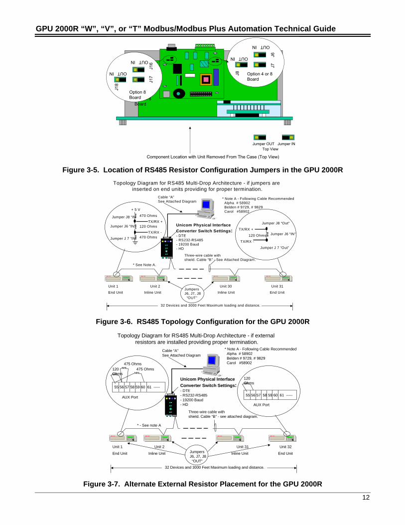
A multi-drop RS485 connection is illustrated in Figure 3-2. Three wires, Positive (Terminal 9), Negative (Terminal8) and Ground (Terminal 10). RS485 requires a termination resistor at each end of the communication cable. Theresistance shall be from 90 to 120 ohms. Additionally, depending upon the RS485 physical interface converterused, a pull-up and pull-down resistor may be added to bias the line to decrease the amount of induced noisecoupled onto the line when no communications are occurring. Internal to the GPU 2000R, are jumpers whichwhen inserted in the proper position (as referenced in Figure 3-5), bias the line by inserting the proper pull-up,pull-down, and termination resistors. To configure the Jumpers J6, J7, and J8, execute the following procedure:
• Refer to Figures 2-4 or 2-5 depending upon the model of Distribution Protection Unit which isinstalled.
• Refer to Figure 3-6 illustrating the placement of J6, J7 and J8 (or J16, J17, or J 18 on a type 8 cardenabling RS 485 for COM 3). J6 (or J16 for COM 3) inserts a 120 ohm resistor between transmit andreceive lines. J7 or (J17 for COM 3) and J8 or (J18 for COM 3) inserts a pull-up and pull-downresistor. The IN position inserts the associated resistor in to the circuit. The OUT position removesthe resistor from the circuit.
• Insert the GPU 2000R unit into the chassis as per the instructions associated with Figures 2-4 or 2-5.• Tighten the knurled screws at the front of the unit.• IT IS advisable to place a sticker on the front of GPU 2000R indicating that it is a terminated
end of line unit. This makes maintenance of installed units easier.
The following example illustrates an interconnection of the GPU 2000R with a host device through a UNICOMphysical interface connection using a 3-wire connection method. It should be noted that the RS485 design onABB relay products incorporates isolation. That is, the RS485 ground is electrically isolated from the internalcircuitry thereby assuring minimal interference from the extreme noise environments found in a substation. Careshould be used when installing an RS485 communication network. The recommended configuration must befollowed as shown in Figure 3-5, 3-6, 3-7, and 3-8. Jumpers J6, J7, and J8 should be inserted to providetermination and pull-up at the GPU 2000R end. Although not shown, a 120 ohm resistor should be insertedbetween the TX/RX + and TX/RX- pairs to provide for termination at the transmission end.
GPU 2000R “W”, “V”, or “T” Modbus/Modbus Plus Automation Technical Guide
12
Jumper OUT Jumper IN Top View
Component Location with Unit Removed From The Case (Top View)
J8
J7
J6
OUT IN
OUT IN
Option 8Board
Option 4 or 8Board
J18
J17
J
16
OUT IN
OUT IN
Option 8Board
Figure 3-5. Location of RS485 Resistor Configuration Jumpers in the GPU 2000R
Unicom Physical Interface Converter Switch Settings:- DTE- RS232-RS485- 19200 Baud- HD
Cable “A”See Attached Diagram
ECEC EC
32 Devices and 3000 Feet Maximum loading and distance.
EC
Unit 1 Unit 2 Unit 30 Unit 31
Three-wire cable withshield. Cable “B” - See Attached Diagram.
End Unit Inline Unit Inline Unit End UnitJumpersJ6, J7, J8 “OUT”
+ 5 V
120 Ohms
470 Ohms
470 Ohms
Jumper J8 “IN
Jumper J 7 “IN”
Jumper J6 “IN”TX/RX +
TX/RX -
Topology Diagram for RS485 Multi-Drop Architecture - if jumpers are inserted on end units providing for proper termination.
* See Note A.
* Note A - Following Cable Recommended Alpha # 58902 Belden # 9729, # 9829 Carol #58902
120 Ohms
Jumper J8 “Out”
Jumper J6 “IN”TX/RX +
TX/RX -
Jumper J 7 “Out”
Figure 3-6. RS485 Topology Configuration for the GPU 2000R
Unicom Physical Interface Converter Switch Settings:- DTE- RS232-RS485- 19200 Baud- HD
Cable “A”See Attached Diagram
ECEC EC
32 Devices and 3000 Feet Maximum loading and distance.
EC
Unit 1 Unit 2 Unit 31 Unit 32
Three-wire cable withshield. Cable “B” - see attached diagram.
End Unit Inline Unit Inline Unit End UnitJumpersJ6, J7, J8 “OUT”
Topology Diagram for RS485 Multi-Drop Architecture - if external resistors are installed providing proper termination.
55 56 57 58 59 60 61 -----
475 Ohms475 Ohms
120Ohms
AUX Port
* - See note A
* Note A - Following Cable Recommended Alpha # 58902 Belden # 9729, # 9829 Carol #58902
55 56 57 58 59 60 61 -----
120Ohms
AUX Port
Figure 3-7. Alternate External Resistor Placement for the GPU 2000R
GPU 2000R “W”, “V”, or “T” Modbus/Modbus Plus Automation Technical Guide
13
TX
+R
X +
TX
-R
X -
GN
D
3
55 56 57 58 59 60 61 -----
RS485 Isolated Port
Shield is isolatedShield is Frame Grounded
at one point
3
55 56 57 58 59 60 61 -----
RS485 Isolated Port
3
55 56 57 58 59 60 61 -----
RS485 Isolated Port
End Unit Inline Unit End Unit
Shield Isolated
Shield isisolated
Cable “B” RS485 Connection
*SeeNote
*Note - Reference the Topology Drawing for Termination configuration if internal or external termination is selected.
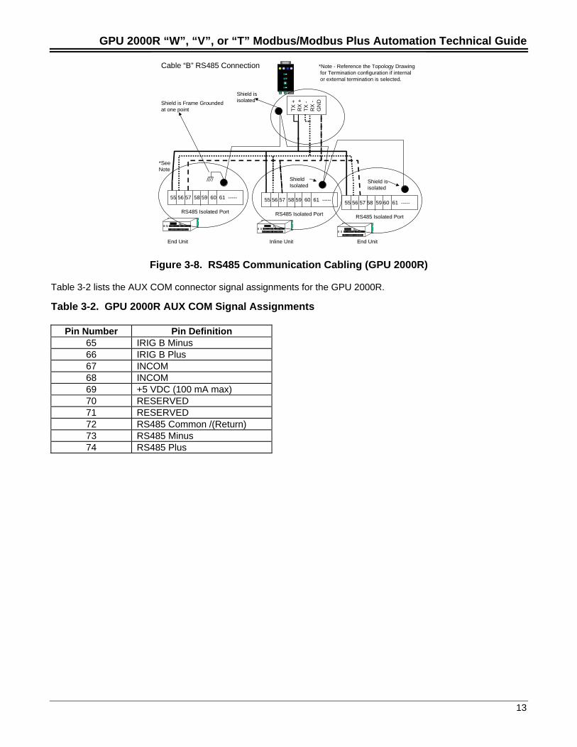
Figure 3-8. RS485 Communication Cabling (GPU 2000R)
Table 3-2 lists the AUX COM connector signal assignments for the GPU 2000R.
Table 3-2. GPU 2000R AUX COM Signal Assignments
Pin Number Pin Definition65 IRIG B Minus66 IRIG B Plus67 INCOM68 INCOM69 +5 VDC (100 mA max)70 RESERVED71 RESERVED72 RS485 Common /(Return)73 RS485 Minus74 RS485 Plus
GPU 2000R “W”, “V”, or “T” Modbus/Modbus Plus Automation Technical Guide
14
Section 4 – GPU 2000R Device Parameterization
Establishing GPU 2000R, communication depends upon correct parameterization of the communication menuswithin the unit. Parameterization may occur via the unit’s front panel interface of through GPU ECP (WindowsExternal Communication Program). Modbus, Modbus Plus and Standard 10 Byte require certainparameterizations. Even COM 0 requires certain parameterization to communication with the configurationprogram.
COM 0 Port (Front Port Configuration)
In order to attach a configuration program to the GPU 2000R, the correct parameters must be set up within theunit. The supported parameters are listed in Table 4-1 below. The protocol for the unit is addressable Standard 10Byte. To view the communication port parameters it is advised that they should be viewed via the unit’s frontpanel interface. If the GPU 2000R does not have a front panel interface, it is recommended that the implementermark the parameters on the front panel sticker with the port’s parameters when installing and commissioning thedevice.
The keystrokes required for visualizing the communication port parameters from the front panel interface are:
1. Depress the “E” pushbutton.
2. Depress the “↓ ” key once to select the SETTINGS Menu and then depress the “E” pushbutton.
3. Depress the “E” pushbutton to select the SHOW SETTINGS Menu selection.
4. Depress the “↓ ” key six times to select the COMMUNICATIONS Menu and then depress the “E” pushbutton.
5. Under the SHOW COM SETTINGS MENU, the following shall be displayed for the Front Panel RS232 port(FP).
Unit Node Address (Address displayed in HEX) FP RS232 Baud FP RS232 Frame
Other parameters shall be shown. The parameters listed shall vary in accordance with the communication cardinserted within the unit. However, the FP displayed parameters must match with the parameters configured in theStandard Ten Byte Section of the ECP package.
One may change parameters via the front panel interface. The selections for each parameter required in FrontPanel Port configuration is shown in Table 4-1.
Table 4-1. GPU 2000R COM Port 0 Front Panel Interface Parameters
Option Selection NotesUnit Node Address 1 to FFF (1 = default setting) 1 to 2048 decimal node addressFP RS232 Baud 300
1200240048009600 (default setting)
Selectable Baud Rates for theStandard Ten Byte Front Panel Port.
FP RS232 Frame N – 8 – 1 (default setting) No Parity 8 Data Bits 1 Stop BitN – 8 – 2 No Parity 8 Data Bits 2 Stop Bits
Modification of the Front Panel Parameter settings is accomplished via the following keystrokes:
1. From the metering menu depress the “E” key.
2. Depress the “↓ ” key once to select the SETTINGS Menu and then depress the “E” pushbutton.
GPU 2000R “W”, “V”, or “T” Modbus/Modbus Plus Automation Technical Guide
15
3. Depress the “↓ ” key once to select the SHOW SETTINGS Menu selection. Depress the “E” pushbutton.
4. Depress the “↓ ” key seven times to select the COMMUNICATIONS Menu and then depress the “E”pushbutton.
5. Enter the unit’s password, one digit at a time. The default password is four spaces. Depress the “E”pushbutton once.
6. The CHANGE COMMUNICATION SETTINGS Menu shall be displayed. With the cursor at the Unit Addressfield, depress “E”. The unit address can be modified. The address selected in this field will configure theaddress for the entire node. Use the “↓ ” and “↑ ” arrow keys to select the password digit entry. Use the “→”and “←” keys to select the digit to configure. Depress “E” to save the digits. Depress “C” to return to the RootMenu.
7. Once returned to the Main Menu, depress the “↓ ” key once to select the FRONT RS232 BAUD RATE Menuand then depress the “E” pushbutton. The selections for the menu are listed in Table 4-1. Use the “→” and“←” keys to select the baud rates for the port. Depress “E” to select the entry. Depress “C” to return to theRoot Menu.
8. Once returned to the Main Menu, depress the “↓ ” key once to select the FRONT RS232 FRAME Menu andthen depress the “E” pushbutton. The selections for the menu are listed in Table 4-1. Use the “→” and “←”keys to select the baud rates for the port. Depress “E” to select the entry. Depress “C” to return to the RootMenu.
9. To Save the selections configured in the previous steps depress the “C” pushbutton. A query will bepresented to the operator “Enter YES to save settings <NO>”. Use the “→” and “←” keys to select the optionYES and depress “E” to save the settings.
If the unit does not have a front panel interface, it is advisable that the communication port parameters be markedon the front of the unit. If the parameters are not known, please contact ABB Technical Support to obtain theprocedure to determine the parameters or take the unit out of service and reset the port parameters.
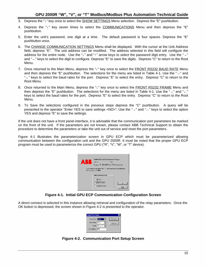
Figure 4-1 illustrates the parameterization screen in GPU ECP which must be parameterized allowingcommunication between the configuration unit and the GPU 2000R. It must be noted that the proper GPU ECPprogram must be used to parameterize the correct GPU (“R”, “V”, “W”, or “T” device).
Figure 4-1. Initial GPU ECP Communication Configuration Screen
A direct connect is selected in this instance allowing retrieval and configuration of the relay parameters. Once theOK button is depressed, the screen shown in Figure 4-2 is presented to the operator.
Figure 4-2. Communication Port Setup Screen
GPU 2000R “W”, “V”, or “T” Modbus/Modbus Plus Automation Technical Guide
16
The selections in GPU ECP are illustrated in Table 4-2. The settings must agree with those configured in theGPU 2000R.
Table 4-2. GPU ECP Communication Port Settings
Option Selection NotesCOM PORT COM 1
COM 2COM 3COM 4
Personal Computer Port Selectionfor ECP to GPU 2000R connection.
BAUD RATE 3001200240048009600 (default setting)19200
Baud Rates Offered for GPU 2000Rconnection to the WinECP RS232port connection.
Frame None – 8 – 1 (default setting) No Parity 8 Data Bits 1 Stop BitNone – 8 – 2 No Parity 8 Data Bits 2 Stop BitsEven – 8 – 1 Even Parity 8 Data Bits 1 Stop BitOdd – 8 – 1 Odd Parity 8 Data Bits 1 Stop BitEven – 7 – 1 Even Parity 7 Data Bits 1 Stop BitNone – 7 – 2 Even Parity 7 Data Bits 2 Stop BitsOdd – 7 – 1 Odd Parity 7 Data Bits 1 Stop Bit
Unit Address 1 – FFF (1 = Default) Unit Address in HEXNOTE : Bold indicates Selections Supported by GPU ECP and GPU 2000R “R”, “W”, “V”, “T” versions
COM Port 1 Option Settings [Catalog 589 XXX00-XXX0 or 589 XXX50-XXX0]
If the unit does not have a front panel interface, the rear port is on the GPU 2000R is active. The Configurationscreens through GPU ECP are shown in Figure 4-3 for reference. The communication options may not beconfigured via the front panel interface since this port is only active if the unit does not have a front panelcommunication port interface (see Section 3 of this document for further information). The communicationprotocol supported on this port is Standard Ten Byte Only.
Table 4-3 illustrates the port configuration options available for this COM Port 1. Figure 4-3 illustrates theWinECP screen used to configure Communication Port 1 in the GPU 2000R.
Table 4-3. COM Port 1 and COM Port 2 GPU ECP Port Setting Options
Option Selection NotesBAUD RATE 300
1200240048009600 (default setting)1920038400
Com Port Baud Rate Selections ViaWinECP or DOS ECP
Frame None – 8 – 1 (default setting) No Parity 8 Data Bits 1 Stop BitNone – 8 – 2 No Parity 8 Data Bits 2 Stop BitsEven – 8 – 1 Even Parity 8 Data Bits 1 Stop BitOdd – 8 – 1 Odd Parity 8 Data Bits 1 Stop BitEven – 7– 1 Even Parity 7 Data Bits 1 Stop BitNone – 7 – 2 Even Parity 7 Data Bits 2 Stop BitsOdd – 7 – 1 Odd Parity 7 Data Bits 1 Stop Bit
GPU 2000R “W”, “V”, or “T” Modbus/Modbus Plus Automation Technical Guide
17
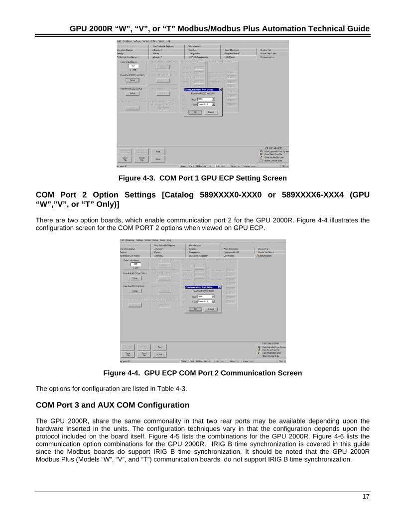
Figure 4-3. COM Port 1 GPU ECP Setting Screen
COM Port 2 Option Settings [Catalog 589XXXX0-XXX0 or 589XXXX6-XXX4 (GPU“W”,”V”, or “T” Only)]
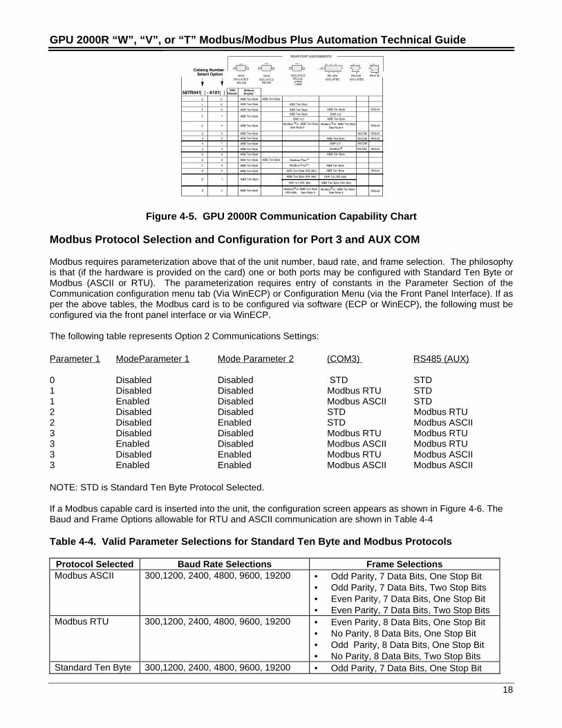
There are two option boards, which enable communication port 2 for the GPU 2000R. Figure 4-4 illustrates theconfiguration screen for the COM PORT 2 options when viewed on GPU ECP.
Figure 4-4. GPU ECP COM Port 2 Communication Screen
The options for configuration are listed in Table 4-3.
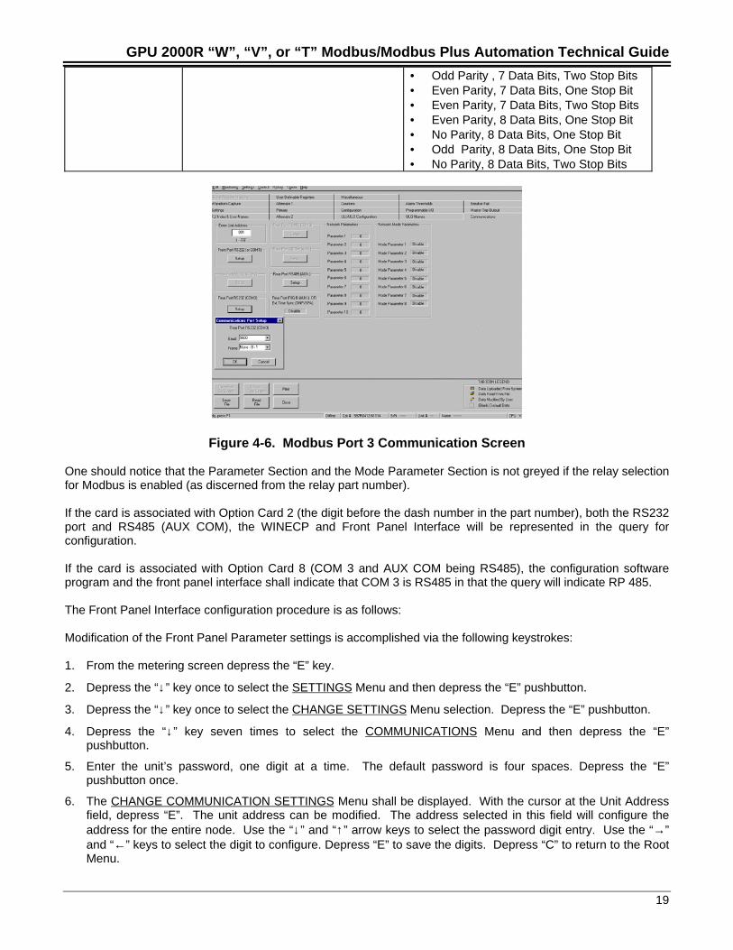
COM Port 3 and AUX COM Configuration
The GPU 2000R, share the same commonality in that two rear ports may be available depending upon thehardware inserted in the units. The configuration techniques vary in that the configuration depends upon theprotocol included on the board itself. Figure 4-5 lists the combinations for the GPU 2000R. Figure 4-6 lists thecommunication option combinations for the GPU 2000R. IRIG B time synchronization is covered in this guidesince the Modbus boards do support IRIG B time synchronization. It should be noted that the GPU 2000RModbus Plus (Models “W”, “V”, and “T”) communication boards do not support IRIG B time synchronization.
GPU 2000R “W”, “V”, or “T” Modbus/Modbus Plus Automation Technical Guide
18
!"#$
%&
%&
%&
%&
%&
%&
%&
!"#$ '#$
!"#$ '#$
( !"#$
) ( !"#$
)
( !"#$*+
& ) ( !"#$
)
!
!"
*+
*+
*+ *+
, %,
%&
-
./
&
0,
0,
0,
0,
0,
&#'$$ !
&&
Figure 4-5. GPU 2000R Communication Capability Chart
Modbus Protocol Selection and Configuration for Port 3 and AUX COM
Modbus requires parameterization above that of the unit number, baud rate, and frame selection. The philosophyis that (if the hardware is provided on the card) one or both ports may be configured with Standard Ten Byte orModbus (ASCII or RTU). The parameterization requires entry of constants in the Parameter Section of theCommunication configuration menu tab (Via WinECP) or Configuration Menu (via the Front Panel Interface). If asper the above tables, the Modbus card is to be configured via software (ECP or WinECP), the following must beconfigured via the front panel interface or via WinECP.
The following table represents Option 2 Communications Settings:
Parameter 1 ModeParameter 1 Mode Parameter 2 (COM3) RS485 (AUX)
0 Disabled Disabled STD STD1 Disabled Disabled Modbus RTU STD1 Enabled Disabled Modbus ASCII STD2 Disabled Disabled STD Modbus RTU2 Disabled Enabled STD Modbus ASCII3 Disabled Disabled Modbus RTU Modbus RTU3 Enabled Disabled Modbus ASCII Modbus RTU3 Disabled Enabled Modbus RTU Modbus ASCII3 Enabled Enabled Modbus ASCII Modbus ASCII
NOTE: STD is Standard Ten Byte Protocol Selected.
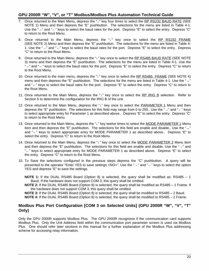
If a Modbus capable card is inserted into the unit, the configuration screen appears as shown in Figure 4-6. TheBaud and Frame Options allowable for RTU and ASCII communication are shown in Table 4-4
Table 4-4. Valid Parameter Selections for Standard Ten Byte and Modbus Protocols
Protocol Selected Baud Rate Selections Frame SelectionsModbus ASCII 300,1200, 2400, 4800, 9600, 19200 • Odd Parity, 7 Data Bits, One Stop Bit
• Odd Parity, 7 Data Bits, Two Stop Bits• Even Parity, 7 Data Bits, One Stop Bit• Even Parity, 7 Data Bits, Two Stop Bits
Modbus RTU 300,1200, 2400, 4800, 9600, 19200 • Even Parity, 8 Data Bits, One Stop Bit• No Parity, 8 Data Bits, One Stop Bit• Odd Parity, 8 Data Bits, One Stop Bit• No Parity, 8 Data Bits, Two Stop Bits
Standard Ten Byte 300,1200, 2400, 4800, 9600, 19200 • Odd Parity, 7 Data Bits, One Stop Bit
GPU 2000R “W”, “V”, or “T” Modbus/Modbus Plus Automation Technical Guide
19
• Odd Parity , 7 Data Bits, Two Stop Bits• Even Parity, 7 Data Bits, One Stop Bit• Even Parity, 7 Data Bits, Two Stop Bits• Even Parity, 8 Data Bits, One Stop Bit• No Parity, 8 Data Bits, One Stop Bit• Odd Parity, 8 Data Bits, One Stop Bit• No Parity, 8 Data Bits, Two Stop Bits
Figure 4-6. Modbus Port 3 Communication Screen
One should notice that the Parameter Section and the Mode Parameter Section is not greyed if the relay selectionfor Modbus is enabled (as discerned from the relay part number).
If the card is associated with Option Card 2 (the digit before the dash number in the part number), both the RS232port and RS485 (AUX COM), the WINECP and Front Panel Interface will be represented in the query forconfiguration.
If the card is associated with Option Card 8 (COM 3 and AUX COM being RS485), the configuration softwareprogram and the front panel interface shall indicate that COM 3 is RS485 in that the query will indicate RP 485.
The Front Panel Interface configuration procedure is as follows:
Modification of the Front Panel Parameter settings is accomplished via the following keystrokes:
1. From the metering screen depress the “E” key.
2. Depress the “↓ ” key once to select the SETTINGS Menu and then depress the “E” pushbutton.
3. Depress the “↓ ” key once to select the CHANGE SETTINGS Menu selection. Depress the “E” pushbutton.
4. Depress the “↓ ” key seven times to select the COMMUNICATIONS Menu and then depress the “E”pushbutton.
5. Enter the unit’s password, one digit at a time. The default password is four spaces. Depress the “E”pushbutton once.
6. The CHANGE COMMUNICATION SETTINGS Menu shall be displayed. With the cursor at the Unit Addressfield, depress “E”. The unit address can be modified. The address selected in this field will configure theaddress for the entire node. Use the “↓ ” and “↑ ” arrow keys to select the password digit entry. Use the “→”and “←” keys to select the digit to configure. Depress “E” to save the digits. Depress “C” to return to the RootMenu.
GPU 2000R “W”, “V”, or “T” Modbus/Modbus Plus Automation Technical Guide
20
7. Once returned to the Main Menu, depress the “↓ ” key four times to select the RP RS232 BAUD RATE (SEENOTE 1) Menu and then depress the “E” pushbutton. The selections for the menu are listed in Table 4-1.Use the “→” and “←” keys to select the baud rates for the port. Depress “E” to select the entry. Depress “C”to return to the Root Menu.
8. Once returned to the Main Menu, depress the “↓ ” key once to select the RP RS232 FRAME (SEE NOTE 2) Menu and then depress the “E” pushbutton. The selections for the menu are listed in Table 4-1. Use the “→” and “←” keys to select the baud rates for the port. Depress “E” to select the entry. Depress“C” to return to the Root Menu.
9. Once returned to the Main Menu, depress the “↓ ” key once to select the RP RS485 BAUD RATE (SEE NOTE3) menu and then depress the “E” pushbutton. The selections for the menu are listed in Table 4-1. Use the“→” and “←” keys to select the baud rates for the port. Depress “E” to select the entry. Depress “C” to returnto the Root Menu.
10. Once returned to the main menu, depress the “↓ ” key once to select the RP RS485 FRAME (SEE NOTE 4)menu and then depress the “E” pushbutton. The selections for the menu are listed in Table 4-1. Use the “→”and “←” keys to select the baud rates for the port. Depress “E” to select the entry. Depress “C” to return tothe Root Menu.
11. Once returned to the Main Menu, depress the “↓ ” key once to select the RP IRIG B selection. Refer toSection 5 to determine the configuration for the IRIG B of the unit.
12. Once returned to the Main Menu, depress the “↓ ” key once to select the PARAMETER 1 Menu and thendepress the “E” pushbutton. The selections for this field may range from 0 to 255.. Use the “→” and “←” keysto select appropriate entry for Parameter 1 as described above.. Depress “E” to select the entry. Depress “C”to return to the Root Menu.
13. Once returned to the Main Menu, depress the “↓ ” key twelve times to select the MODE PARAMETER 1 Menuitem and then depress the “E” pushbutton. The selections for this field are enable and disable.. Use the “→”and “←” keys to select appropriate entry for MODE PARAMETER 1 as described above.. Depress “E” toselect the entry. Depress “C” to return to the Root Menu.
14. Once returned to the Main Menu, depress the “↓ ” key once to select the MODE PARAMETER 2 Menu itemand then depress the “E” pushbutton. The selections for this field are enable and disable. Use the “→” and“←” keys to select appropriate entry for MODE PARAMETER 1 as described above. Depress “E” to selectthe entry. Depress “C” to return to the Root Menu.
15. To Save the selections configured in the previous steps depress the “C” pushbutton. A query will bepresented to the operator “Enter YES to save settings <NO>”. Use the “→” and “←” keys to select the optionYES and depress “E” to save the settings.
NOTE 1: If the DUAL RS485 Board (Option 8) is selected, the query shall be modified as: RS485 – 1Baud. If the hardware does not support COM 3, this query shall be omitted.
NOTE 2: If the DUAL RS485 Board (Option 8) is selected, the query shall be modified as RS485 – 1 Frame. Ifthe hardware does not support COM 3, this query shall be omitted.
NOTE 3: If the DUAL RS485 Board (Option 8) is selected, the query shall be modified to RS485 – 2 Baud.NOTE 4: If the DUAL RS485 Board (Option 8) is selected, the query shall be modified to RS485 – 2 Frame.
Modbus Plus Port Configuration [COM 3 on Selected Units] (GPU 2000R “W”, “V”, “T”Only)
Only the GPU 2000R supports Modbus Plus. The GPU 2000R recognizes if the communication card supportsModbus Plus. Only the Unit Address field within the communication port parameter screen is used via ModbusPlus. One should refer later sections in this manual for a further explanation of the Modbus Plus addressingscheme for accessing relay information.
GPU 2000R “W”, “V”, or “T” Modbus/Modbus Plus Automation Technical Guide
21
IRIG B Configuration and Wiring
Although not a protocol, IRIG B time synchronization is included on the communication cards within the GPU2000R. The following section describes the theory, connection and configuration options present within the GPU2000R.
IRIG B is a time code, which allows devices across the world to synchronize with a common time source to aresolution of one millisecond. IRIG B allows each device to synchronize with the frame received by an IRIG Breceiver. ABB’s DPU/TPU/GPU 2000/R relays (herein referred to as an IED) offer IRIG B time synchronizationcapabilities.
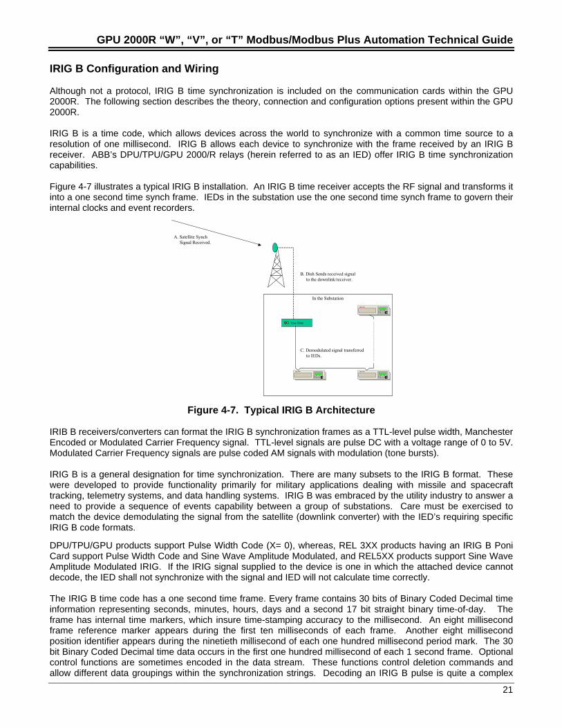
Figure 4-7 illustrates a typical IRIG B installation. An IRIG B time receiver accepts the RF signal and transforms itinto a one second time synch frame. IEDs in the substation use the one second time synch frame to govern theirinternal clocks and event recorders.
In the Substation
True Time
EC
EC
EC
A. Satellite Synch Signal Received.
B. Dish Sends received signal to the downlink/receiver.
C. Demodulated signal transferred to IEDs.
Figure 4-7. Typical IRIG B Architecture
IRIB B receivers/converters can format the IRIG B synchronization frames as a TTL-level pulse width, ManchesterEncoded or Modulated Carrier Frequency signal. TTL-level signals are pulse DC with a voltage range of 0 to 5V.Modulated Carrier Frequency signals are pulse coded AM signals with modulation (tone bursts).
IRIG B is a general designation for time synchronization. There are many subsets to the IRIG B format. Thesewere developed to provide functionality primarily for military applications dealing with missile and spacecrafttracking, telemetry systems, and data handling systems. IRIG B was embraced by the utility industry to answer aneed to provide a sequence of events capability between a group of substations. Care must be exercised tomatch the device demodulating the signal from the satellite (downlink converter) with the IED’s requiring specificIRIG B code formats.
DPU/TPU/GPU products support Pulse Width Code (X= 0), whereas, REL 3XX products having an IRIG B PoniCard support Pulse Width Code and Sine Wave Amplitude Modulated, and REL5XX products support Sine WaveAmplitude Modulated IRIG. If the IRIG signal supplied to the device is one in which the attached device cannotdecode, the IED shall not synchronize with the signal and IED will not calculate time correctly.
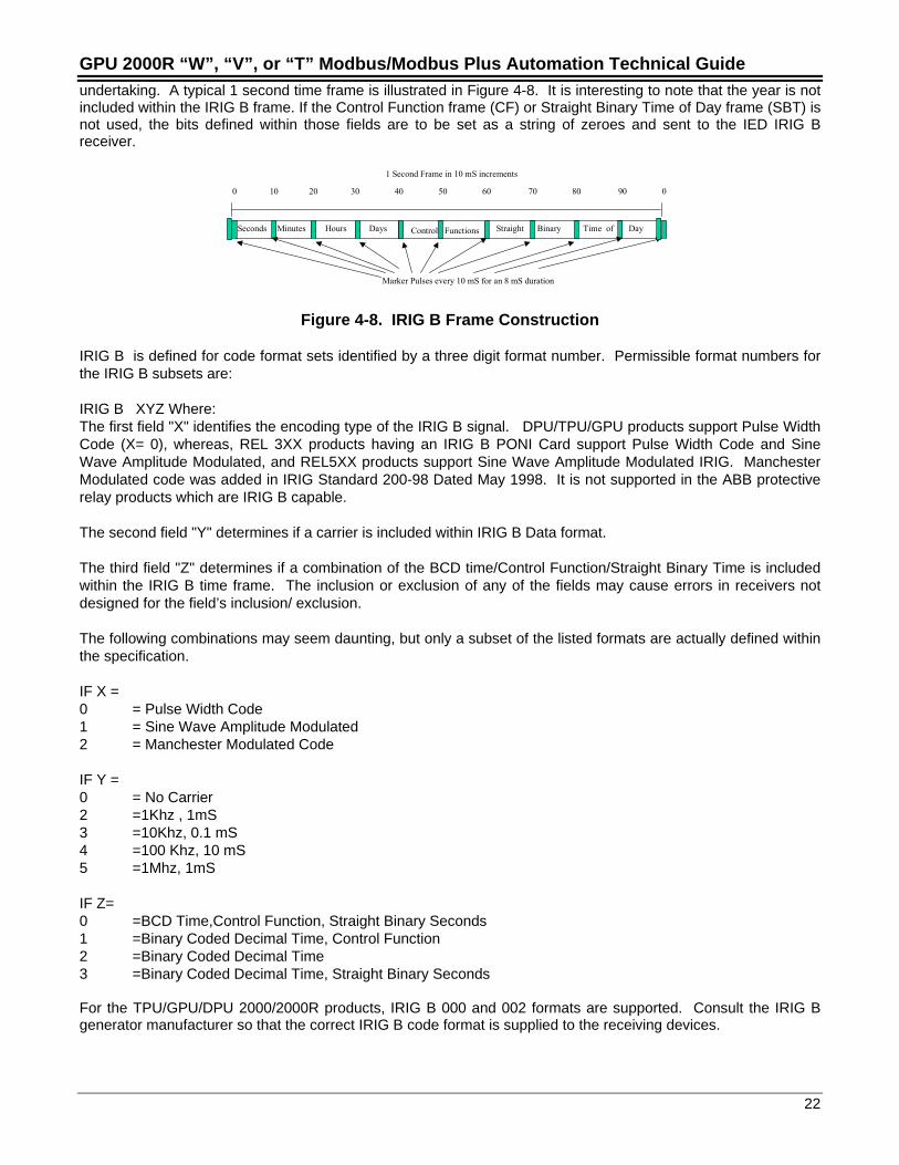
The IRIG B time code has a one second time frame. Every frame contains 30 bits of Binary Coded Decimal timeinformation representing seconds, minutes, hours, days and a second 17 bit straight binary time-of-day. Theframe has internal time markers, which insure time-stamping accuracy to the millisecond. An eight millisecondframe reference marker appears during the first ten milliseconds of each frame. Another eight millisecondposition identifier appears during the ninetieth millisecond of each one hundred millisecond period mark. The 30bit Binary Coded Decimal time data occurs in the first one hundred millisecond of each 1 second frame. Optionalcontrol functions are sometimes encoded in the data stream. These functions control deletion commands andallow different data groupings within the synchronization strings. Decoding an IRIG B pulse is quite a complex
GPU 2000R “W”, “V”, or “T” Modbus/Modbus Plus Automation Technical Guide
22
undertaking. A typical 1 second time frame is illustrated in Figure 4-8. It is interesting to note that the year is notincluded within the IRIG B frame. If the Control Function frame (CF) or Straight Binary Time of Day frame (SBT) isnot used, the bits defined within those fields are to be set as a string of zeroes and sent to the IED IRIG Breceiver.
Seconds Minutes Hours Days Control Functions Straight Binary Time of Day
0 10 20 30 40 50 60 70 80 90 0
Marker Pulses every 10 mS for an 8 mS duration
1 Second Frame in 10 mS increments
Figure 4-8. IRIG B Frame Construction
IRIG B is defined for code format sets identified by a three digit format number. Permissible format numbers forthe IRIG B subsets are:
IRIG B XYZ Where:The first field "X" identifies the encoding type of the IRIG B signal. DPU/TPU/GPU products support Pulse WidthCode (X= 0), whereas, REL 3XX products having an IRIG B PONI Card support Pulse Width Code and SineWave Amplitude Modulated, and REL5XX products support Sine Wave Amplitude Modulated IRIG. ManchesterModulated code was added in IRIG Standard 200-98 Dated May 1998. It is not supported in the ABB protectiverelay products which are IRIG B capable.
The second field "Y" determines if a carrier is included within IRIG B Data format.
The third field "Z" determines if a combination of the BCD time/Control Function/Straight Binary Time is includedwithin the IRIG B time frame. The inclusion or exclusion of any of the fields may cause errors in receivers notdesigned for the field’s inclusion/ exclusion.
The following combinations may seem daunting, but only a subset of the listed formats are actually defined withinthe specification.
IF X =0 = Pulse Width Code1 = Sine Wave Amplitude Modulated2 = Manchester Modulated Code
IF Y =0 = No Carrier2 =1Khz , 1mS3 =10Khz, 0.1 mS4 =100 Khz, 10 mS5 =1Mhz, 1mS
IF Z=0 =BCD Time,Control Function, Straight Binary Seconds1 =Binary Coded Decimal Time, Control Function2 =Binary Coded Decimal Time3 =Binary Coded Decimal Time, Straight Binary Seconds
For the TPU/GPU/DPU 2000/2000R products, IRIG B 000 and 002 formats are supported. Consult the IRIG Bgenerator manufacturer so that the correct IRIG B code format is supplied to the receiving devices.
GPU 2000R “W”, “V”, or “T” Modbus/Modbus Plus Automation Technical Guide
23
Hardware Configuration
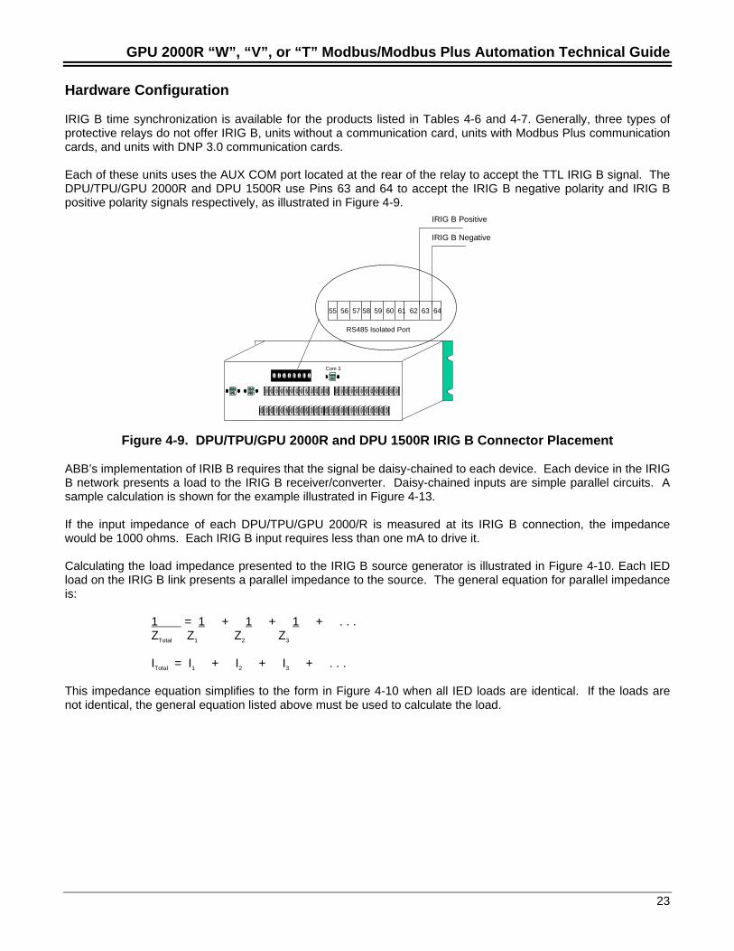
IRIG B time synchronization is available for the products listed in Tables 4-6 and 4-7. Generally, three types ofprotective relays do not offer IRIG B, units without a communication card, units with Modbus Plus communicationcards, and units with DNP 3.0 communication cards.
Each of these units uses the AUX COM port located at the rear of the relay to accept the TTL IRIG B signal. TheDPU/TPU/GPU 2000R and DPU 1500R use Pins 63 and 64 to accept the IRIG B negative polarity and IRIG Bpositive polarity signals respectively, as illustrated in Figure 4-9.
Com 3
55 56 57 58 59 60 61 62 63 64
RS485 Isolated Port
IRIG B Positive
IRIG B Negative
Figure 4-9. DPU/TPU/GPU 2000R and DPU 1500R IRIG B Connector Placement
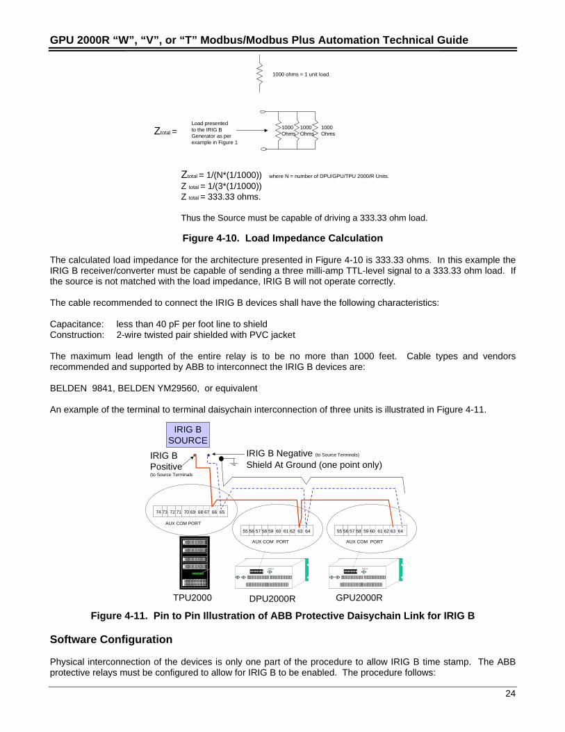
ABB’s implementation of IRIB B requires that the signal be daisy-chained to each device. Each device in the IRIGB network presents a load to the IRIG B receiver/converter. Daisy-chained inputs are simple parallel circuits. Asample calculation is shown for the example illustrated in Figure 4-13.
If the input impedance of each DPU/TPU/GPU 2000/R is measured at its IRIG B connection, the impedancewould be 1000 ohms. Each IRIG B input requires less than one mA to drive it.
Calculating the load impedance presented to the IRIG B source generator is illustrated in Figure 4-10. Each IEDload on the IRIG B link presents a parallel impedance to the source. The general equation for parallel impedanceis:
1 = 1 + 1 + 1 + . . .ZTotal Z1 Z2 Z3
ITotal = I1 + I2 + I3 + . . .
This impedance equation simplifies to the form in Figure 4-10 when all IED loads are identical. If the loads arenot identical, the general equation listed above must be used to calculate the load.
GPU 2000R “W”, “V”, or “T” Modbus/Modbus Plus Automation Technical Guide
24
1000 ohms = 1 unit load.
Load presentedto the IRIG BGenerator as perexample in Figure 1
1000Ohms
1000Ohms
1000Ohms
Ztotal = 1/(N*(1/1000)) where N = number of DPU/GPU/TPU 2000/R Units.
Z total = 1/(3*(1/1000))Z total = 333.33 ohms.
Thus the Source must be capable of driving a 333.33 ohm load.
Ztotal =
Figure 4-10. Load Impedance Calculation
The calculated load impedance for the architecture presented in Figure 4-10 is 333.33 ohms. In this example theIRIG B receiver/converter must be capable of sending a three milli-amp TTL-level signal to a 333.33 ohm load. Ifthe source is not matched with the load impedance, IRIG B will not operate correctly.
The cable recommended to connect the IRIG B devices shall have the following characteristics:
Capacitance: less than 40 pF per foot line to shieldConstruction: 2-wire twisted pair shielded with PVC jacket
The maximum lead length of the entire relay is to be no more than 1000 feet. Cable types and vendorsrecommended and supported by ABB to interconnect the IRIG B devices are:
BELDEN 9841, BELDEN YM29560, or equivalent
An example of the terminal to terminal daisychain interconnection of three units is illustrated in Figure 4-11.
74 73 72 71 70 69 68 67 66 65
AUX COM PORT
IRIG BSOURCE
TPU2000
Com 3
55 56 57 58 59 60 61 62 63 64
AUX COM PORT
DPU2000R
Com 3
55 56 57 58 59 60 61 62 63 64
AUX COM PORT
GPU2000R
IRIG B Negative (to Source Terminals)IRIG BPositive(to Source Terminals
Shield At Ground (one point only)
Figure 4-11. Pin to Pin Illustration of ABB Protective Daisychain Link for IRIG B
Software Configuration
Physical interconnection of the devices is only one part of the procedure to allow IRIG B time stamp. The ABBprotective relays must be configured to allow for IRIG B to be enabled. The procedure follows:
GPU 2000R “W”, “V”, or “T” Modbus/Modbus Plus Automation Technical Guide
25
1. Start GPU ECP from the operating system for the appropriate device being configured.2. Highlight the Change Settings Menu.3. Highlight and Select the Communications Menu.4. Scroll down to the field “ IRIG B”.
Depress the enter key and select the “ENABLE” selection. Two selections are displayed, ENABLE-mmm orENABLE-cc. When IRIGB time is enabled for the AUX COMM board, two settings are available forcommunicating the time to a host device. If (IRIGB cc) is selected then all times received from the GPU 2000Rwill be in the Hour:Minute:Second:Hundreds of Seconds format. If (IRIGB mmm) is selected then all times will betransmitted as an unsigned long word where the most significant bit is set to 1 and the remainder of the long wordwill represent the total milli-seconds for the day.
Example: The following (IRIGB mmm) time is received from the GPU2000R:
82C6F096, where hour contains 82, minute contains C6 etc.
This would represent the following time in hours minutes seconds milliseconds:
12:56:13:150
The above was changed for version 3.21 of GPU.We have now only Enable/Disable Rear Port IRIG from the Settings/Communications.All records (Fault, Fault Summary and Operations) have time format hh:mm:ss:xxx when IRIG-B isenabled and hh:mm:ss:xx0 when IRIG-B is disabled.
5. Return from the menu item.6. Download the changed selections to the attached unit.
The unit is now synchronized to the IRIG B time source. All events shall be time stamped to the common IRIG Btime source. The protective relays may also be configured for IRIG B timestamping from the front panel MMI ofunits which are equipped with a front panel interface.
GPU 2000R “W”, “V”, or “T” Modbus/Modbus Plus Automation Technical Guide
26
Section 5 - Modbus
Modbus is available in two emulation’s, Modbus RTU and Modbus ASCII. Modbus RTU is a bit oriented protocol(normally referred to as Synchronous), and Modbus ASCII is a byte oriented protocol (normally referred to asAsynchronous). Both emulations support the same command set. Networked nodes cannot communicateunless the same emulation of the Modbus protocol is interpreted. This is an extremely important issue. TheGPU 2000R supports the Modbus ASCII and RTU protocol emulations.
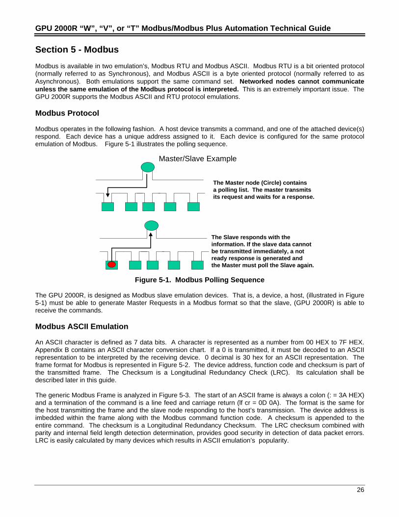
Modbus Protocol
Modbus operates in the following fashion. A host device transmits a command, and one of the attached device(s)respond. Each device has a unique address assigned to it. Each device is configured for the same protocolemulation of Modbus. Figure 5-1 illustrates the polling sequence.
Master/Slave Example
The Master node (Circle) containsa polling list. The master transmitsits request and waits for a response.
The Slave responds with the information. If the slave data cannot be transmitted immediately, a not ready response is generated and the Master must poll the Slave again.
Figure 5-1. Modbus Polling Sequence
The GPU 2000R, is designed as Modbus slave emulation devices. That is, a device, a host, (illustrated in Figure5-1) must be able to generate Master Requests in a Modbus format so that the slave, (GPU 2000R) is able toreceive the commands.
Modbus ASCII Emulation
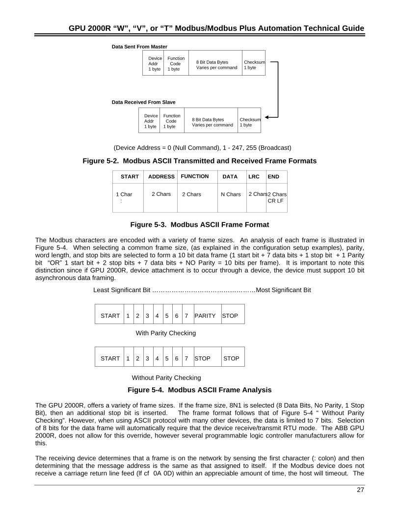
An ASCII character is defined as 7 data bits. A character is represented as a number from 00 HEX to 7F HEX.Appendix B contains an ASCII character conversion chart. If a 0 is transmitted, it must be decoded to an ASCIIrepresentation to be interpreted by the receiving device. 0 decimal is 30 hex for an ASCII representation. Theframe format for Modbus is represented in Figure 5-2. The device address, function code and checksum is part ofthe transmitted frame. The Checksum is a Longitudinal Redundancy Check (LRC). Its calculation shall bedescribed later in this guide.
The generic Modbus Frame is analyzed in Figure 5-3. The start of an ASCII frame is always a colon (: = 3A HEX)and a termination of the command is a line feed and carriage return (lf cr = 0D 0A). The format is the same forthe host transmitting the frame and the slave node responding to the host’s transmission. The device address isimbedded within the frame along with the Modbus command function code. A checksum is appended to theentire command. The checksum is a Longitudinal Redundancy Checksum. The LRC checksum combined withparity and internal field length detection determination, provides good security in detection of data packet errors.LRC is easily calculated by many devices which results in ASCII emulation’s popularity.
GPU 2000R “W”, “V”, or “T” Modbus/Modbus Plus Automation Technical Guide
27
DeviceAddr1 byte
Function Code1 byte
8 Bit Data BytesVaries per command
Checksum1 byte
DeviceAddr1 byte
Function Code1 byte
8 Bit Data BytesVaries per command
Checksum1 byte
Data Sent From Master
Data Received From Slave
(Device Address = 0 (Null Command), 1 - 247, 255 (Broadcast)
Figure 5-2. Modbus ASCII Transmitted and Received Frame Formats
START FUNCTIONADDRESS DATA LRC END
1 Char :
2 Chars 2 Chars N Chars 2 Chars2 CharsCR LF
Figure 5-3. Modbus ASCII Frame Format
The Modbus characters are encoded with a variety of frame sizes. An analysis of each frame is illustrated inFigure 5-4. When selecting a common frame size, (as explained in the configuration setup examples), parity,word length, and stop bits are selected to form a 10 bit data frame (1 start bit + 7 data bits + 1 stop bit + 1 Paritybit “OR” 1 start bit + 2 stop bits + 7 data bits + NO Parity = 10 bits per frame). It is important to note thisdistinction since if GPU 2000R, device attachment is to occur through a device, the device must support 10 bitasynchronous data framing.
Least Significant Bit …………………………………………Most Significant Bit
START 1 2 3 4 5 6 7 PARITY STOP
With Parity Checking
START 1 2 3 4 5 6 7 STOP STOP
Without Parity Checking
Figure 5-4. Modbus ASCII Frame Analysis
The GPU 2000R, offers a variety of frame sizes. If the frame size, 8N1 is selected (8 Data Bits, No Parity, 1 StopBit), then an additional stop bit is inserted. The frame format follows that of Figure 5-4 “ Without ParityChecking”. However, when using ASCII protocol with many other devices, the data is limited to 7 bits. Selectionof 8 bits for the data frame will automatically require that the device receive/transmit RTU mode. The ABB GPU2000R, does not allow for this override, however several programmable logic controller manufacturers allow forthis.
The receiving device determines that a frame is on the network by sensing the first character (: colon) and thendetermining that the message address is the same as that assigned to itself. If the Modbus device does notreceive a carriage return line feed (lf cf 0A 0D) within an appreciable amount of time, the host will timeout. The
GPU 2000R “W”, “V”, or “T” Modbus/Modbus Plus Automation Technical Guide
28
length of characters in the message determines Timeout. Modbus ASCII will timeout is the time delay betweeneach character exceeds 1 second delay between each character’s transmission. If 100 characters are required totransmit a complete Modbus ASCII frame, then the timeout for the message could be in excess of 100 secondsfor that specific exchange.
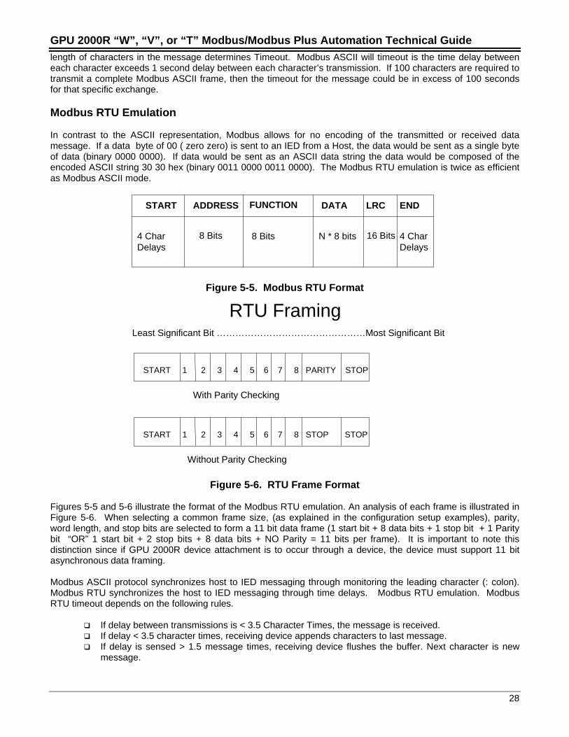
Modbus RTU Emulation
In contrast to the ASCII representation, Modbus allows for no encoding of the transmitted or received datamessage. If a data byte of 00 ( zero zero) is sent to an IED from a Host, the data would be sent as a single byteof data (binary 0000 0000). If data would be sent as an ASCII data string the data would be composed of theencoded ASCII string 30 30 hex (binary 0011 0000 0011 0000). The Modbus RTU emulation is twice as efficientas Modbus ASCII mode.
START FUNCTIONADDRESS DATA LRC END
4 CharDelays
8 Bits 8 Bits N * 8 bits 16 Bits 4 CharDelays
Figure 5-5. Modbus RTU Format
RTU FramingLeast Significant Bit …………………………………………Most Significant Bit
With Parity Checking
Without Parity Checking
START 1 2 3 4 5 6 7 8 PARITY STOP
START 1 2 3 4 5 6 7 8 STOP STOP
Figure 5-6. RTU Frame Format
Figures 5-5 and 5-6 illustrate the format of the Modbus RTU emulation. An analysis of each frame is illustrated inFigure 5-6. When selecting a common frame size, (as explained in the configuration setup examples), parity,word length, and stop bits are selected to form a 11 bit data frame (1 start bit + 8 data bits + 1 stop bit + 1 Paritybit “OR” 1 start bit + 2 stop bits + 8 data bits + NO Parity = 11 bits per frame). It is important to note thisdistinction since if GPU 2000R device attachment is to occur through a device, the device must support 11 bitasynchronous data framing.
Modbus ASCII protocol synchronizes host to IED messaging through monitoring the leading character (: colon).Modbus RTU synchronizes the host to IED messaging through time delays. Modbus RTU emulation. ModbusRTU timeout depends on the following rules.
If delay between transmissions is < 3.5 Character Times, the message is received. If delay < 3.5 character times, receiving device appends characters to last message. If delay is sensed > 1.5 message times, receiving device flushes the buffer. Next character is new
message.
GPU 2000R “W”, “V”, or “T” Modbus/Modbus Plus Automation Technical Guide
29
The Modbus RTU emulation senses timeouts quicker than the Modbus ASCII emulation. The Modbus RTUemulation also uses a CRC –16 checksum in contrast to the Modbus ASCII using a LRC (LongitudinalRedundancy Check). The CRC –16 is a much more robust checksum. With parity, internal protocol messagelength field checks and the CRC-16, the error detection is exceptional.
IMPLEMENTATION TIP-When commissioning a Modbus system, it is always advisable to connect acommunication analyzer in-line with the host. It is always uncertain whether the host is sending thecommand correctly. Within the GPU 2000R, an incorrect address request will always generate anexception response from the relay. If an exception response is generated, many host devices will notdisplay the Modbus exception response generated by the unit. A communication analyzer allows for rapidtroubleshooting of a malfunctioning network connection.
Modbus Plus (Available on the GPU 2000R “W”, “V” and “T” Only)
Modbus capabilities were expanded in a significant way during the late 1980’s. The base command set was notchanged from the Modbus protocol, however, the protocol access method was modified. The limitations ofModbus exposed themselves in a few areas:
The throughput was dependent upon the physical interface (RS232 and 485) which limited the speed ofdata transfer.
The Modbus protocol did not efficiently manage its bandwidth. Exorbitant amounts of time could bespent waiting for the slave device to respond with data or timeout.
The Modbus protocol only allowed connection of a single host (or multiple hosts with the addition ofhardware multiplexers) to up to 247 IEDs.
The originator of the protocol Modicon AEG, had devised a way to use the Modbus protocol and present it to theattached nodes to eliminate the deficiencies found in large Modbus installations.
Modbus Plus was developed using a proprietary physical interface allowing communication over a twistedshielded pair medium. The baud rate of the network was fixed at 1 megabaud. If this had been the only changefrom Modbus to Modbus Plus, the network’s introduction would not have been significant. The Modbusrepackaging into a Modbus Plus format afforded the following significant benefits:
Up to 34 simultaneous conversations may occur on a network. Each device on a Modbus network is capable of being a host. Each device may broadcast a data, which is received by all other nodes on the network. Node to node network throughput time may be deterministically calculated.
The Modbus Plus interface was afforded though the manufacturer entering into a “MODCONNECTAGREEMENT” allowing sharing of technology between the IED implementers and Modicon AEG. The IEDimplementers received Modbus Plus chipsets and technology allowing network implementation. Once theimplementation was completed, a certification process ensued and upon the IED’s successful test of theimplementation, certification was bestowed upon the IED.
Modbus Plus Theory of Operation
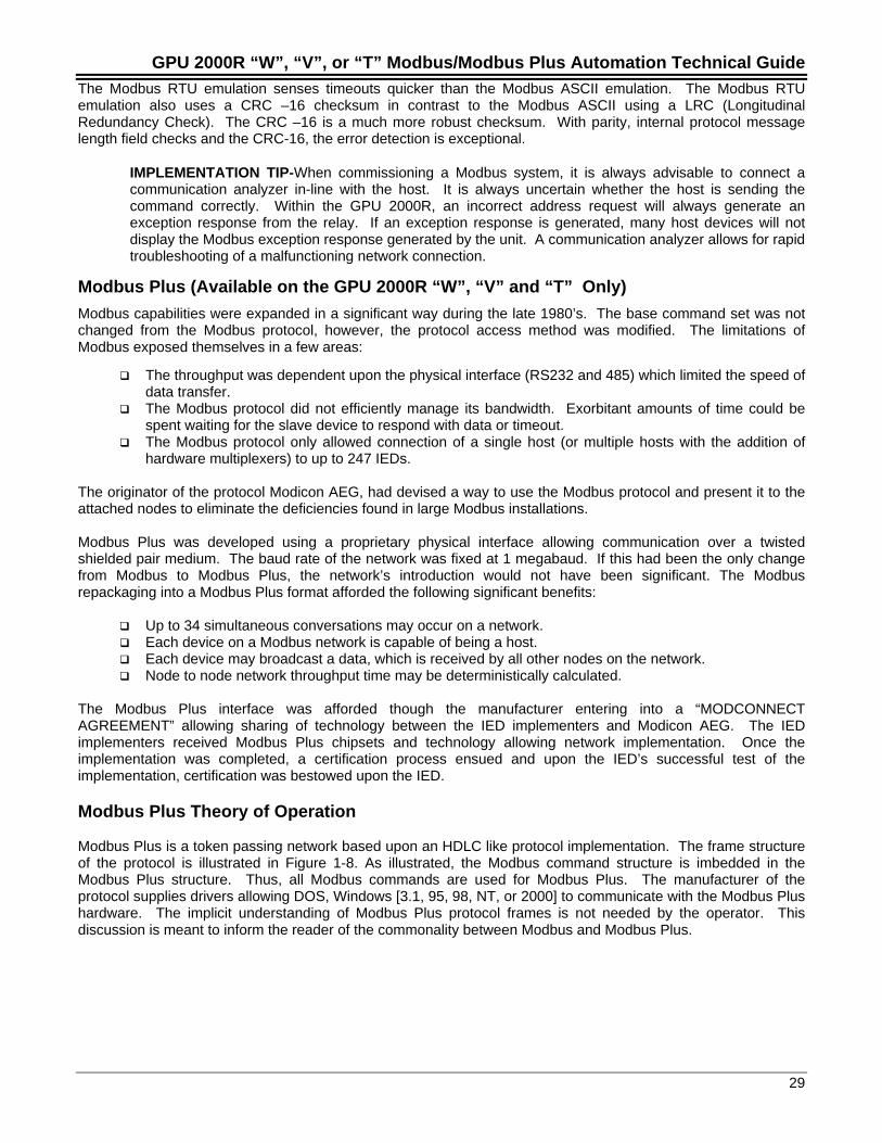
Modbus Plus is a token passing network based upon an HDLC like protocol implementation. The frame structureof the protocol is illustrated in Figure 1-8. As illustrated, the Modbus command structure is imbedded in theModbus Plus structure. Thus, all Modbus commands are used for Modbus Plus. The manufacturer of theprotocol supplies drivers allowing DOS, Windows [3.1, 95, 98, NT, or 2000] to communicate with the Modbus Plushardware. The implicit understanding of Modbus Plus protocol frames is not needed by the operator. Thisdiscussion is meant to inform the reader of the commonality between Modbus and Modbus Plus.
GPU 2000R “W”, “V”, or “T” Modbus/Modbus Plus Automation Technical Guide
30
PREAMBLE AA
OPENING FLAG 7E(SYNCH FLAG)
BROADCAST ADDR FF
CRC-16FRAMECHECK
CLOSING FLAG
MESSAGEPREAMBLE AA
OPENING FLAG 7E(SYNCH FLAG)
BROADCAST ADDR FF
CRC-16FRAMECHECK
CLOSING FLAG
MESSAGE
DEST ADDRESS
SOURCEADDRESS
FUNCTION CODE
COMMAND INCLUSION( INCLUDES MODBUS)
MASTEROUTPUTPATH
ROUTERCOUNTER
TRANSSEQUENCE NUMBER
ROUTING PATH
MODBUS FRAME
MAC
Figure 5-7. Modbus Plus Message Frame Structure
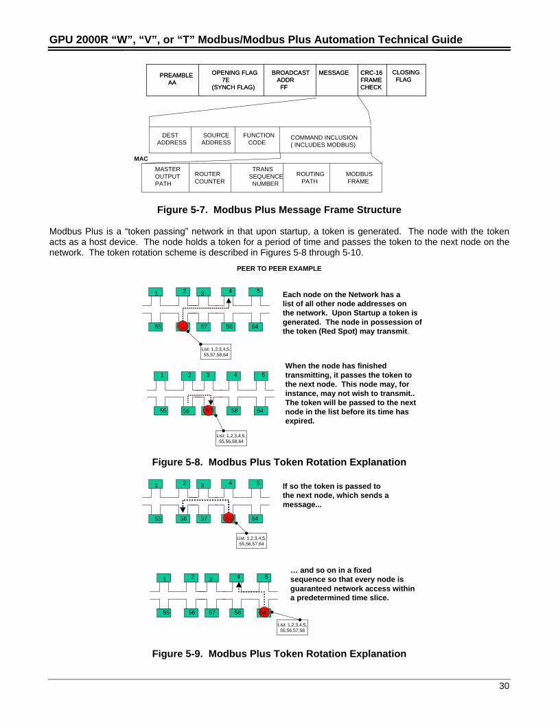
Modbus Plus is a “token passing” network in that upon startup, a token is generated. The node with the tokenacts as a host device. The node holds a token for a period of time and passes the token to the next node on thenetwork. The token rotation scheme is described in Figures 5-8 through 5-10.
PEER TO PEER EXAMPLE
Each node on the Network has alist of all other node addresses onthe network. Upon Startup a token isgenerated. The node in possession ofthe token (Red Spot) may transmit.
When the node has finishedtransmitting, it passes the token tothe next node. This node may, for instance, may not wish to transmit.. The token will be passed to the next node in the list before its time has expired.
1 2 3 4 5
55 57 58 64
1 2 3 4 5
55 57 58 6456
List: 1,2,3,4,5,55,57,58,64
List: 1,2,3,4,5,55,56,58,64
56
Figure 5-8. Modbus Plus Token Rotation Explanation
If so the token is passed tothe next node, which sends a message...
… and so on in a fixedsequence so that every node is guaranteed network access withina predetermined time slice.
1 2 3 4 5
55 57 6456 58
1 2 3 4 5
55 5756 58 64
List: 1,2,3,4,5,55,56,57,64
List: 1,2,3,4,5,55,56,57,58
Figure 5-9. Modbus Plus Token Rotation Explanation
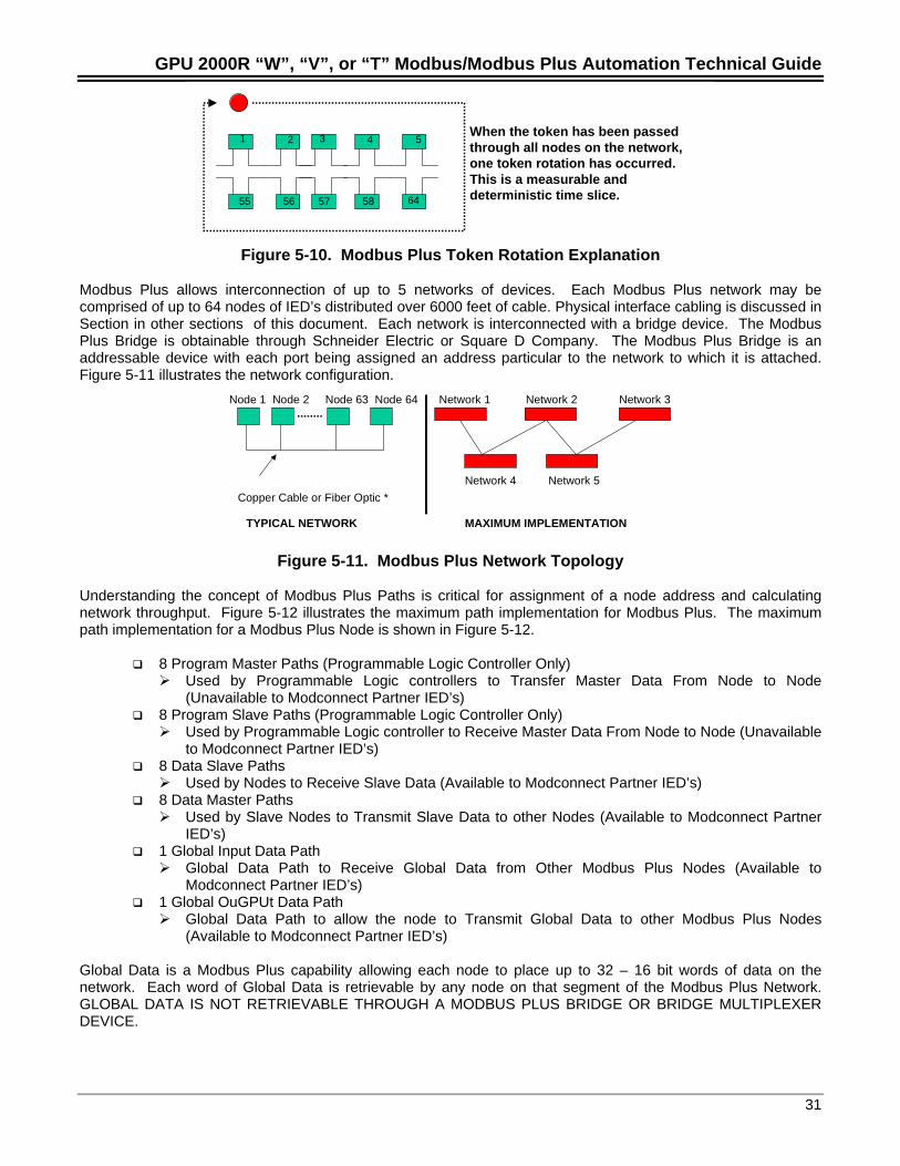
GPU 2000R “W”, “V”, or “T” Modbus/Modbus Plus Automation Technical Guide
31
1 2 3 4 5
55 5756 58 64
When the token has been passed through all nodes on the network, one token rotation has occurred. This is a measurable and deterministic time slice.
Figure 5-10. Modbus Plus Token Rotation Explanation
Modbus Plus allows interconnection of up to 5 networks of devices. Each Modbus Plus network may becomprised of up to 64 nodes of IED’s distributed over 6000 feet of cable. Physical interface cabling is discussed inSection in other sections of this document. Each network is interconnected with a bridge device. The ModbusPlus Bridge is obtainable through Schneider Electric or Square D Company. The Modbus Plus Bridge is anaddressable device with each port being assigned an address particular to the network to which it is attached.Figure 5-11 illustrates the network configuration.
Node 1 Node 2 Node 63 Node 64
Copper Cable or Fiber Optic *
Network 1 Network 2 Network 3
Network 4 Network 5
TYPICAL NETWORK MAXIMUM IMPLEMENTATION
Figure 5-11. Modbus Plus Network Topology
Understanding the concept of Modbus Plus Paths is critical for assignment of a node address and calculatingnetwork throughput. Figure 5-12 illustrates the maximum path implementation for Modbus Plus. The maximumpath implementation for a Modbus Plus Node is shown in Figure 5-12.
8 Program Master Paths (Programmable Logic Controller Only) Used by Programmable Logic controllers to Transfer Master Data From Node to Node
(Unavailable to Modconnect Partner IED’s) 8 Program Slave Paths (Programmable Logic Controller Only)
Used by Programmable Logic controller to Receive Master Data From Node to Node (Unavailableto Modconnect Partner IED’s)
8 Data Slave Paths Used by Nodes to Receive Slave Data (Available to Modconnect Partner IED’s)
8 Data Master Paths Used by Slave Nodes to Transmit Slave Data to other Nodes (Available to Modconnect Partner
IED’s) 1 Global Input Data Path
Global Data Path to Receive Global Data from Other Modbus Plus Nodes (Available toModconnect Partner IED’s)
1 Global OuGPUt Data Path Global Data Path to allow the node to Transmit Global Data to other Modbus Plus Nodes
(Available to Modconnect Partner IED’s)
Global Data is a Modbus Plus capability allowing each node to place up to 32 – 16 bit words of data on thenetwork. Each word of Global Data is retrievable by any node on that segment of the Modbus Plus Network.GLOBAL DATA IS NOT RETRIEVABLE THROUGH A MODBUS PLUS BRIDGE OR BRIDGE MULTIPLEXERDEVICE.
GPU 2000R “W”, “V”, or “T” Modbus/Modbus Plus Automation Technical Guide
32
Modbus Plus Node (Maximum Implementation)
8 Data Master Paths
8 Data Slave Paths
Global Data Read Global Data Write
8 Program Master Paths 8 Program Slave Paths
EC
8 Data Slave Paths
Global Data Out
Figure 5-12. Modbus Plus Path Designation
The GPU 2000R implementation of Modbus Plus shows the data path implementation. The GPU 2000R ModbusPlus implementation allows:
The GPU 2000R to receive information requests from a device acting as a host along one ofits 8 data slave paths.
The GPU 2000R to place up to 32 registers of data on the Global Out Data Path. The datasent on the Global Out Path is configurable through ECP or WinECP. The ConfigurationMethod is described in Section 4.
The GPU 2000R implements Modbus PLUS as a HOST device. The Modbus Plus address assignment requireddepends upon the understanding of the path assignment discussion. Figure 5-13 illustrates the addressingrequired when a device (such as a programmable logic controller or a host device with a Modbus Plus SA 85card) must access a GPU 2000R via Modbus Plus. An application note is included in Appendix C describing theprocess for Programmable Logic Controller attachment with a GPU 2000R. This application note can easily beapplied in connecting a GPU 2000R to a Programmable Logic Controller Network.
As per Figure 5-13, if a host device X is to request data from an ABB GPU 2000R, the node address (configuredvia the front panel interface, ECP, or WinECP) is the first address node entry in the data path for the addressRouting Path 1. In the case with the nodes sharing the same network, the Routing Path 2 entry is the slave pathaddress communicated with. The Route address for the slave path is 1 through 8.
Routing Addr 1 Routing Addr 2 Routing Addr 3 Routing Addr 4 Routing Addr 55 1 0 0 0
64 Nodes Maximum with 6000’ of cable
1500 ‘ Repeater 1500’ Repeater 1500 ‘ Repeater 1500 ‘
1500 ‘ Repeater 1500’ Repeater 1500 ‘ Repeater 1500 ‘
Bridge
Bridge
1
64
1
64
12
3 4 5 6 27 28 29 21 22 23 24 25 26 42 52
2
12
22 32
Segment 1 Segment 2 Segment 3 Segment 4
= Line Termination
31 30 3 34 52 53 29 28 35 7 8 9 NETWORK 1
NETWORK 2
X Q
ZW
From X (Host) to Q (DPU 2000R) = Same network = 28.A.0.0.0From X (Host) to Z = Thru Networks = 1.22.A.0.0From X(Host) to N = Thru Networks = 1.1.33.A.0From W (Host) to Z = Thru Networks = 1.12.A.0.0(NOTE A = Slave Path Number from 1 to 8)
33
N
Figure 5-13. Modbus Plus Addressing Example
GPU 2000R “W”, “V”, or “T” Modbus/Modbus Plus Automation Technical Guide
33
If a node had to cross a network boundary through a Bridge, the examples illustrate how node access addressingwould be affected.
Modbus and Modbus Plus General Notes
Modbus is an exceptional protocol for bridging a majority of vendor devices to communicate to each other. Thegeneration of each protocol, throughput, robust capabilities and troubleshooting techniques shall be covered inlater sections. The understanding of each of these principles shall aid the implement in exploiting the capabilitieswithin their own automation system.
Modbus ASCII, Modbus RTU, and Modbus Plus have the following capacities implemented within the GPU2000R.
01 - Read 0X Coil Status 02 - Read 1X Contact Status 03 - Read 4X Holding Registers 06 - Preset Single 4X Holding Register (GPU 2000R “W”, “V”, “T” Versions only) 16 - Write 4X Holding Registers 08 - Diagnostics 23 - Write 4X and Read 4X Holding Registers 20 - Read 6X Extended Registers 21 - Write 6X Extended Registers
The GPU 2000R emulates a slave device. Any other Modbus command sent to the GPU 2000R shall result in aModbus exception code being sent to the transmitting device. The following sections will further describe theModbus functionality within the GPU 2000R.
IMPLEMENTATION TIP-Although the GPU 2000R allows configuration of Modbus for a Frame of N-8-1,some implementations will interpret this emulation of Modbus to be RTU Mode. The GPU 2000R does notsupport this mode. It is advisable to contact the manufacturer of the host and host software to determine theinterpretation of the command string. For example, the Modicon XMIT and COMM BLOCK allowing the PLCto emulate a host device only allows block frame size designation of 7 data bits.
0X Data Map Definitions
Modbus/Modbus Plus Register Map
0X Discrete Coils
Discrete Modbus Coil status is available via a function 01 request via Modbus. Figure 5-14 illustrates a typicalcommand sequence. The Host polls the GPU 2000R for the Data. The GPU 2000R receives the request andresponds with the expected data. The Host then interprets the command response, checks the checksum (LRCif ASCII, CRC 16 if RTU mode) and then displays the interpreted data. Additional information is available inModicon’s protocol manual references listed at the beginning of this document. One must remember that the GPU2000R “R” version has a different memory map than that of the GPU 2000R “W”, “V”, or “T” IED’s.
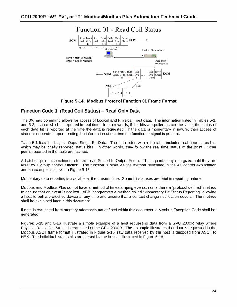
GPU 2000R “W”, “V”, or “T” Modbus/Modbus Plus Automation Technical Guide
34
Function 01 - Read Coil Status
Modbus Host
EC
Modbus Slave Addr =1
Read from 0X Mapping
SlaveAddr.
Funct.Code 01
StartAddrHI
Start Addr LO
CoilsRead HI
CoilsRead LO
ErrorCheck EOMSOM
SlaveAddr.
Funct.Code 01
ByteCount *
DataByte 1
…..DataByte NNN
ErrorCheck EOMSOM
Byte 1 …2……..3…….4…….5……6……..7….
MSB LSB
8 7 6 5 4 3 2 1
SOM = Start of MessageEOM = End of Message
Figure 5-14. Modbus Protocol Function 01 Frame Format
Function Code 1 (Read Coil Status) – Read Only Data
The 0X read command allows for access of Logical and Physical Input data. The information listed in Tables 5-1,and 5-2, is that which is reported in real time. In other words, if the bits are polled as per the table, the status ofeach data bit is reported at the time the data is requested. If the data is momentary in nature, then access ofstatus is dependent upon reading the information at the time the function or signal is present.
Table 5-1 lists the Logical Ouput Single Bit Data. The data listed within the table includes real time status bitswhich may be briefly reported status bits. In other words, they follow the real time status of the point. Otherpoints reported in the table are latched.
A Latched point (sometimes referred to as Sealed In Output Point). These points stay energized until they arereset by a group control function. The function is reset via the method described in the 4X control explanationand an example is shown in Figure 5-18.
Momentary data reporting is available at the present time. Some bit statuses are brief in reporting nature.
Modbus and Modbus Plus do not have a method of timestamping events, nor is there a “protocol defined” methodto ensure that an event is not lost. ABB incorporates a method called “Momentary Bit Status Reporting” allowinga host to poll a protective device at any time and ensure that a contact change notification occurs. The methodshall be explained later in this document.
If data is requested from memory addresses not defined within this document, a Modbus Exception Code shall begenerated
Figures 5-15 and 5-16 illustrate a simple example of a host requesting data from a GPU 2000R relay wherePhysical Relay Coil Status is requested of the GPU 2000R. The example illustrates that data is requested in theModbus ASCII frame format illustrated in Figure 5-15, raw data received by the host is decoded from ASCII toHEX. The individual status bits are parsed by the host as illustrated in Figure 5-16.
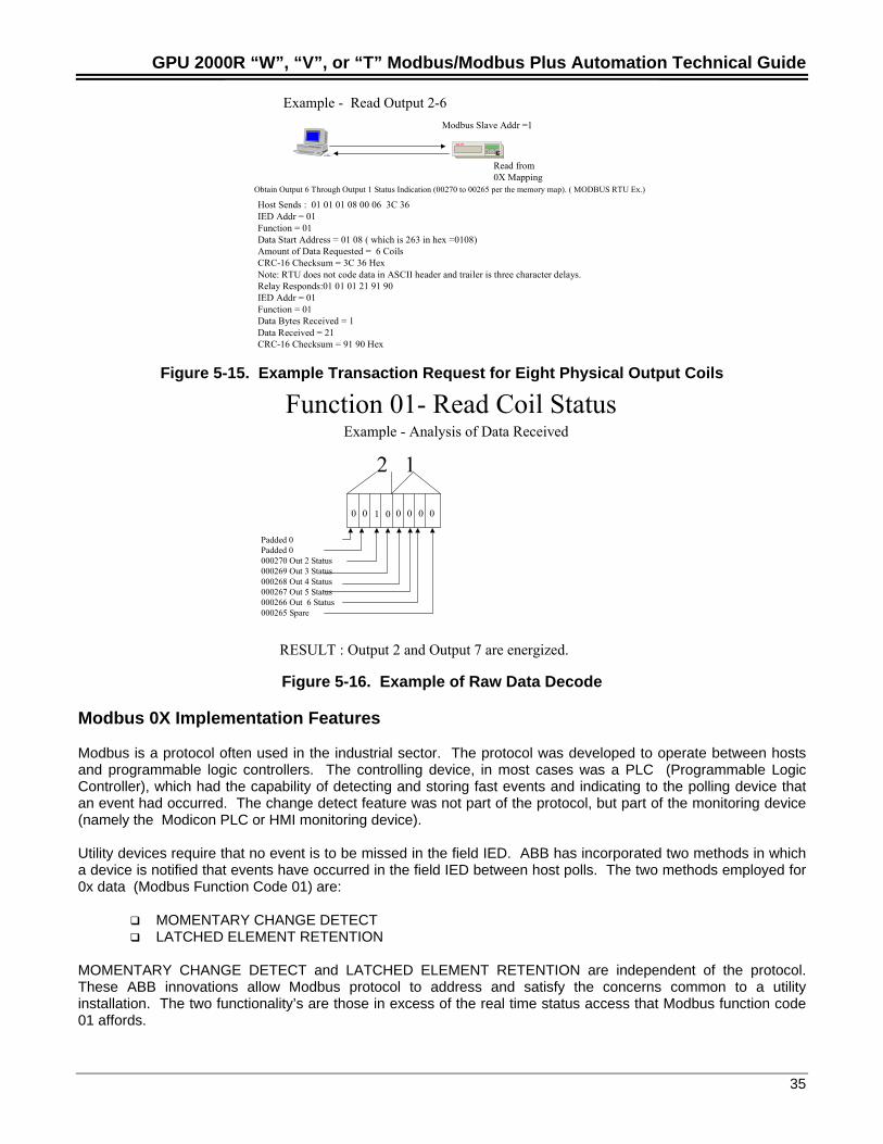
GPU 2000R “W”, “V”, or “T” Modbus/Modbus Plus Automation Technical Guide
35
Example - Read Output 2-6
Obtain Output 6 Through Output 1 Status Indication (00270 to 00265 per the memory map). ( MODBUS RTU Ex.)
Host Sends : 01 01 01 08 00 06 3C 36IED Addr = 01Function = 01Data Start Address = 01 08 ( which is 263 in hex =0108)Amount of Data Requested = 6 CoilsCRC-16 Checksum = 3C 36 HexNote: RTU does not code data in ASCII header and trailer is three character delays.Relay Responds:01 01 01 21 91 90IED Addr = 01Function = 01Data Bytes Received = 1Data Received = 21CRC-16 Checksum = 91 90 Hex
Modbus Slave Addr =1
Read from 0X Mapping
EC
Figure 5-15. Example Transaction Request for Eight Physical Output Coils
Function 01- Read Coil Status
0 0 1 0 0 0 0 0
Example - Analysis of Data Received
2 1
Padded 0Padded 0000270 Out 2 Status000269 Out 3 Status000268 Out 4 Status000267 Out 5 Status000266 Out 6 Status000265 Spare
RESULT : Output 2 and Output 7 are energized.
Figure 5-16. Example of Raw Data Decode
Modbus 0X Implementation Features
Modbus is a protocol often used in the industrial sector. The protocol was developed to operate between hostsand programmable logic controllers. The controlling device, in most cases was a PLC (Programmable LogicController), which had the capability of detecting and storing fast events and indicating to the polling device thatan event had occurred. The change detect feature was not part of the protocol, but part of the monitoring device(namely the Modicon PLC or HMI monitoring device).
Utility devices require that no event is to be missed in the field IED. ABB has incorporated two methods in whicha device is notified that events have occurred in the field IED between host polls. The two methods employed for0x data (Modbus Function Code 01) are:
MOMENTARY CHANGE DETECT LATCHED ELEMENT RETENTION
MOMENTARY CHANGE DETECT and LATCHED ELEMENT RETENTION are independent of the protocol.These ABB innovations allow Modbus protocol to address and satisfy the concerns common to a utilityinstallation. The two functionality’s are those in excess of the real time status access that Modbus function code01 affords.
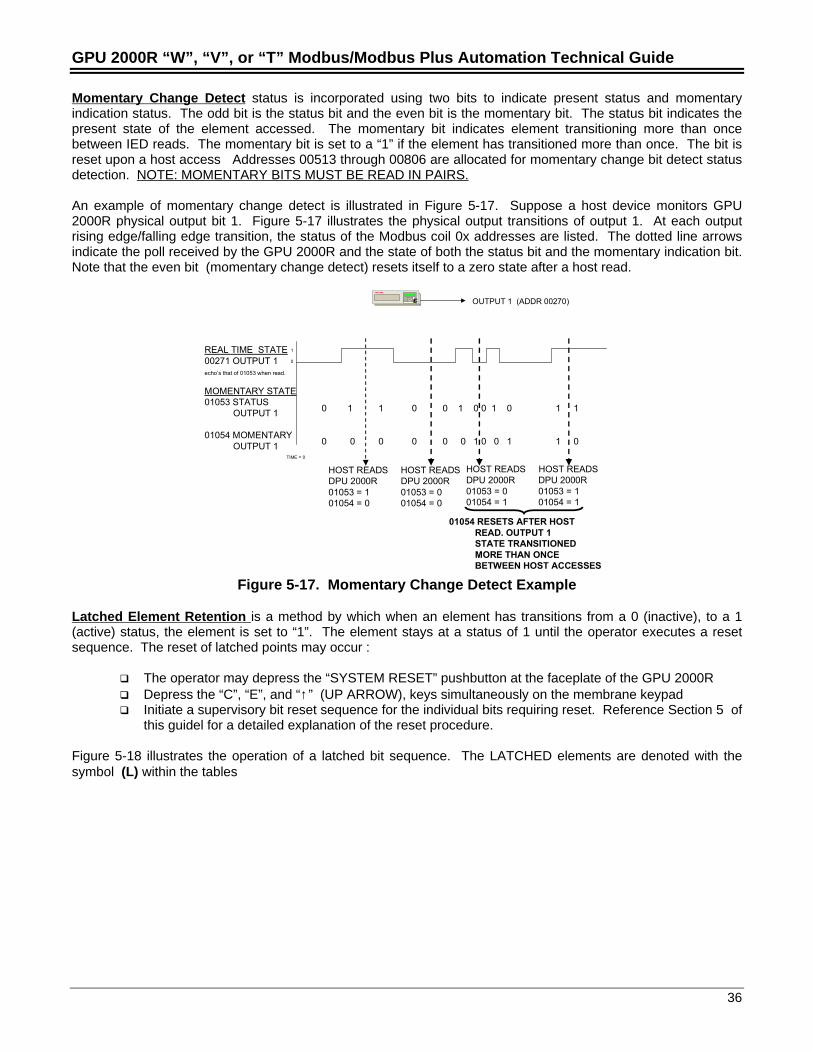
GPU 2000R “W”, “V”, or “T” Modbus/Modbus Plus Automation Technical Guide
36
Momentary Change Detect status is incorporated using two bits to indicate present status and momentaryindication status. The odd bit is the status bit and the even bit is the momentary bit. The status bit indicates thepresent state of the element accessed. The momentary bit indicates element transitioning more than oncebetween IED reads. The momentary bit is set to a “1” if the element has transitioned more than once. The bit isreset upon a host access Addresses 00513 through 00806 are allocated for momentary change bit detect statusdetection. NOTE: MOMENTARY BITS MUST BE READ IN PAIRS.
An example of momentary change detect is illustrated in Figure 5-17. Suppose a host device monitors GPU2000R physical output bit 1. Figure 5-17 illustrates the physical output transitions of output 1. At each outputrising edge/falling edge transition, the status of the Modbus coil 0x addresses are listed. The dotted line arrowsindicate the poll received by the GPU 2000R and the state of both the status bit and the momentary indication bit.Note that the even bit (momentary change detect) resets itself to a zero state after a host read.
EC OUTPUT 1 (ADDR 00270)
REAL TIME STATE00271 OUTPUT 1echo’s that of 01053 when read.
1
0
MOMENTARY STATE01053 STATUS
OUTPUT 1
01054 MOMENTARYOUTPUT 1
TIME = 0
0 1 1 0 0 1 0 0 1 0 1 1
0 0 0 0 0 0 1 0 0 1 1 0
HOST READSDPU 2000R01053 = 101054 = 0
HOST READSDPU 2000R01053 = 001054 = 0
HOST READS HOST READSDPU 2000R DPU 2000R01053 = 0 01053 = 101054 = 1 01054 = 1
01054 RESETS AFTER HOSTREAD. OUTPUT 1 STATE TRANSITIONEDMORE THAN ONCE BETWEEN HOST ACCESSES
Figure 5-17. Momentary Change Detect Example
Latched Element Retention is a method by which when an element has transitions from a 0 (inactive), to a 1(active) status, the element is set to “1”. The element stays at a status of 1 until the operator executes a resetsequence. The reset of latched points may occur :
The operator may depress the “SYSTEM RESET” pushbutton at the faceplate of the GPU 2000R Depress the “C”, “E”, and “↑ ” (UP ARROW), keys simultaneously on the membrane keypad Initiate a supervisory bit reset sequence for the individual bits requiring reset. Reference Section 5 of
this guidel for a detailed explanation of the reset procedure.
Figure 5-18 illustrates the operation of a latched bit sequence. The LATCHED elements are denoted with thesymbol (L) within the tables
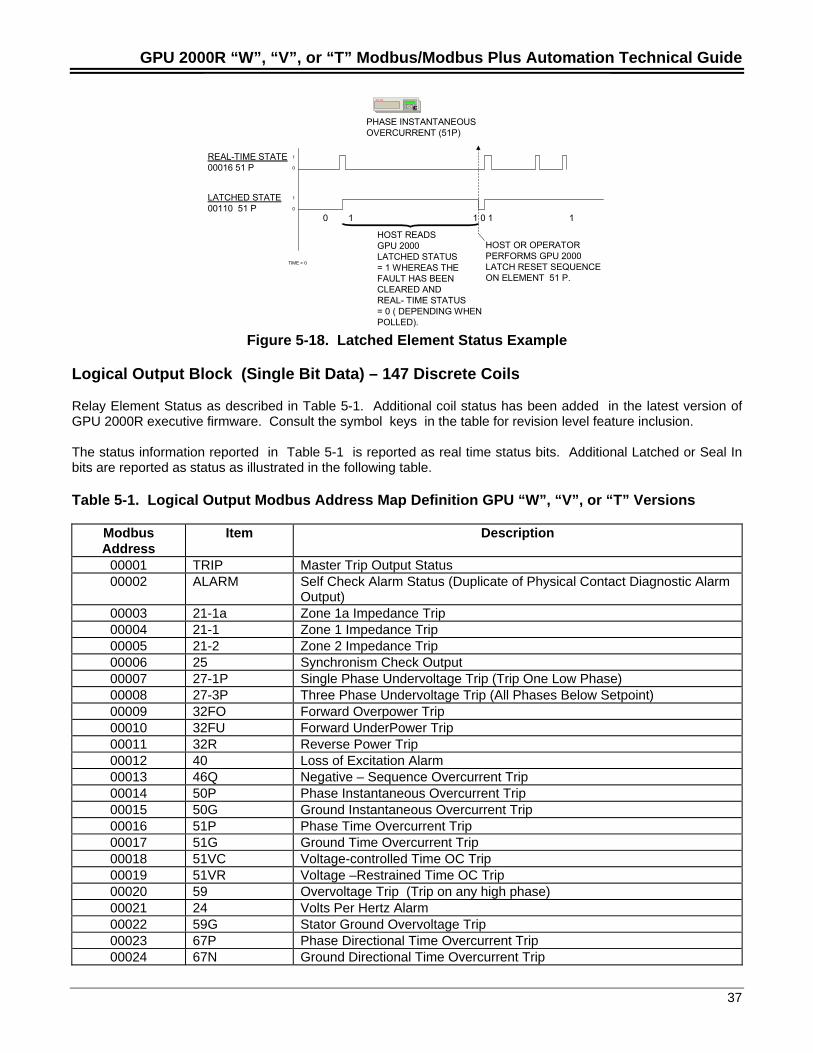
GPU 2000R “W”, “V”, or “T” Modbus/Modbus Plus Automation Technical Guide
37
EC
REAL-TIME STATE00016 51 P
1
0
LATCHED STATE00110 51 P
TIME = 0
0 1 1 0 1 1
HOST READSGPU 2000LATCHED STATUS= 1 WHEREAS THEFAULT HAS BEENCLEARED ANDREAL- TIME STATUS= 0 ( DEPENDING WHENPOLLED).
HOST OR OPERATOR PERFORMS GPU 2000 LATCH RESET SEQUENCE ON ELEMENT 51 P.
PHASE INSTANTANEOUSOVERCURRENT (51P)
1
0
Figure 5-18. Latched Element Status Example
Logical Output Block (Single Bit Data) – 147 Discrete Coils
Relay Element Status as described in Table 5-1. Additional coil status has been added in the latest version ofGPU 2000R executive firmware. Consult the symbol keys in the table for revision level feature inclusion.
The status information reported in Table 5-1 is reported as real time status bits. Additional Latched or Seal Inbits are reported as status as illustrated in the following table.
Table 5-1. Logical Output Modbus Address Map Definition GPU “W”, “V”, or “T” Versions
ModbusAddress
Item Description
00001 TRIP Master Trip Output Status00002 ALARM Self Check Alarm Status (Duplicate of Physical Contact Diagnostic Alarm
Output)00003 21-1a Zone 1a Impedance Trip00004 21-1 Zone 1 Impedance Trip00005 21-2 Zone 2 Impedance Trip00006 25 Synchronism Check Output00007 27-1P Single Phase Undervoltage Trip (Trip One Low Phase)00008 27-3P Three Phase Undervoltage Trip (All Phases Below Setpoint)00009 32FO Forward Overpower Trip00010 32FU Forward UnderPower Trip00011 32R Reverse Power Trip00012 40 Loss of Excitation Alarm00013 46Q Negative – Sequence Overcurrent Trip00014 50P Phase Instantaneous Overcurrent Trip00015 50G Ground Instantaneous Overcurrent Trip00016 51P Phase Time Overcurrent Trip00017 51G Ground Time Overcurrent Trip00018 51VC Voltage-controlled Time OC Trip00019 51VR Voltage –Restrained Time OC Trip00020 59 Overvoltage Trip (Trip on any high phase)00021 24 Volts Per Hertz Alarm00022 59G Stator Ground Overvoltage Trip00023 67P Phase Directional Time Overcurrent Trip00024 67N Ground Directional Time Overcurrent Trip
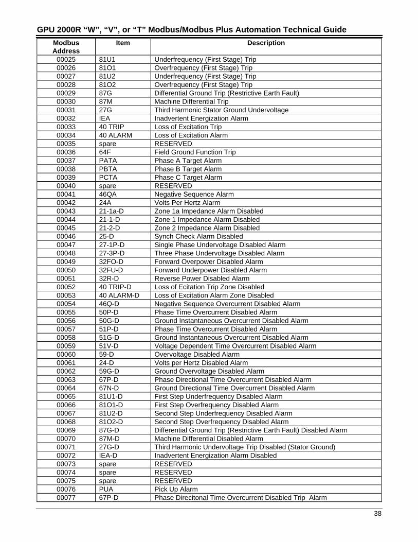
GPU 2000R “W”, “V”, or “T” Modbus/Modbus Plus Automation Technical Guide
38
ModbusAddress
Item Description
00025 81U1 Underfrequency (First Stage) Trip00026 81O1 Overfrequency (First Stage) Trip00027 81U2 Underfrequency (First Stage) Trip00028 81O2 Overfrequency (First Stage) Trip00029 87G Differential Ground Trip (Restrictive Earth Fault)00030 87M Machine Differential Trip00031 27G Third Harmonic Stator Ground Undervoltage00032 IEA Inadvertent Energization Alarm00033 40 TRIP Loss of Excitation Trip00034 40 ALARM Loss of Excitation Alarm00035 spare RESERVED00036 64F Field Ground Function Trip00037 PATA Phase A Target Alarm00038 PBTA Phase B Target Alarm00039 PCTA Phase C Target Alarm00040 spare RESERVED00041 46QA Negative Sequence Alarm00042 24A Volts Per Hertz Alarm00043 21-1a-D Zone 1a Impedance Alarm Disabled00044 21-1-D Zone 1 Impedance Alarm Disabled00045 21-2-D Zone 2 Impedance Alarm Disabled00046 25-D Synch Check Alarm Disabled00047 27-1P-D Single Phase Undervoltage Disabled Alarm00048 27-3P-D Three Phase Undervoltage Disabled Alarm00049 32FO-D Forward Overpower Disabled Alarm00050 32FU-D Forward Underpower Disabled Alarm00051 32R-D Reverse Power Disabled Alarm00052 40 TRIP-D Loss of Ecitation Trip Zone Disabled00053 40 ALARM-D Loss of Excitation Alarm Zone Disabled00054 46Q-D Negative Sequence Overcurrent Disabled Alarm00055 50P-D Phase Time Overcurrent Disabled Alarm00056 50G-D Ground Instantaneous Overcurrent Disabled Alarm00057 51P-D Phase Time Overcurrent Disabled Alarm00058 51G-D Ground Instantaneous Overcurrent Disabled Alarm00059 51V-D Voltage Dependent Time Overcurrent Disabled Alarm00060 59-D Overvoltage Disabled Alarm00061 24-D Volts per Hertz Disabled Alarm00062 59G-D Ground Overvoltage Disabled Alarm00063 67P-D Phase Directional Time Overcurrent Disabled Alarm00064 67N-D Ground Directional Time Overcurrent Disabled Alarm00065 81U1-D First Step Underfrequency Disabled Alarm00066 81O1-D First Step Overfrequency Disabled Alarm00067 81U2-D Second Step Underfrequency Disabled Alarm00068 81O2-D Second Step Overfrequency Disabled Alarm00069 87G-D Differential Ground Trip (Restrictive Earth Fault) Disabled Alarm00070 87M-D Machine Differential Disabled Alarm00071 27G-D Third Harmonic Undervoltage Trip Disabled (Stator Ground)00072 IEA-D Inadvertent Energization Alarm Disabled00073 spare RESERVED00074 spare RESERVED00075 spare RESERVED00076 PUA Pick Up Alarm00077 67P-D Phase Direcitonal Time Overcurrent Disabled Trip Alarm
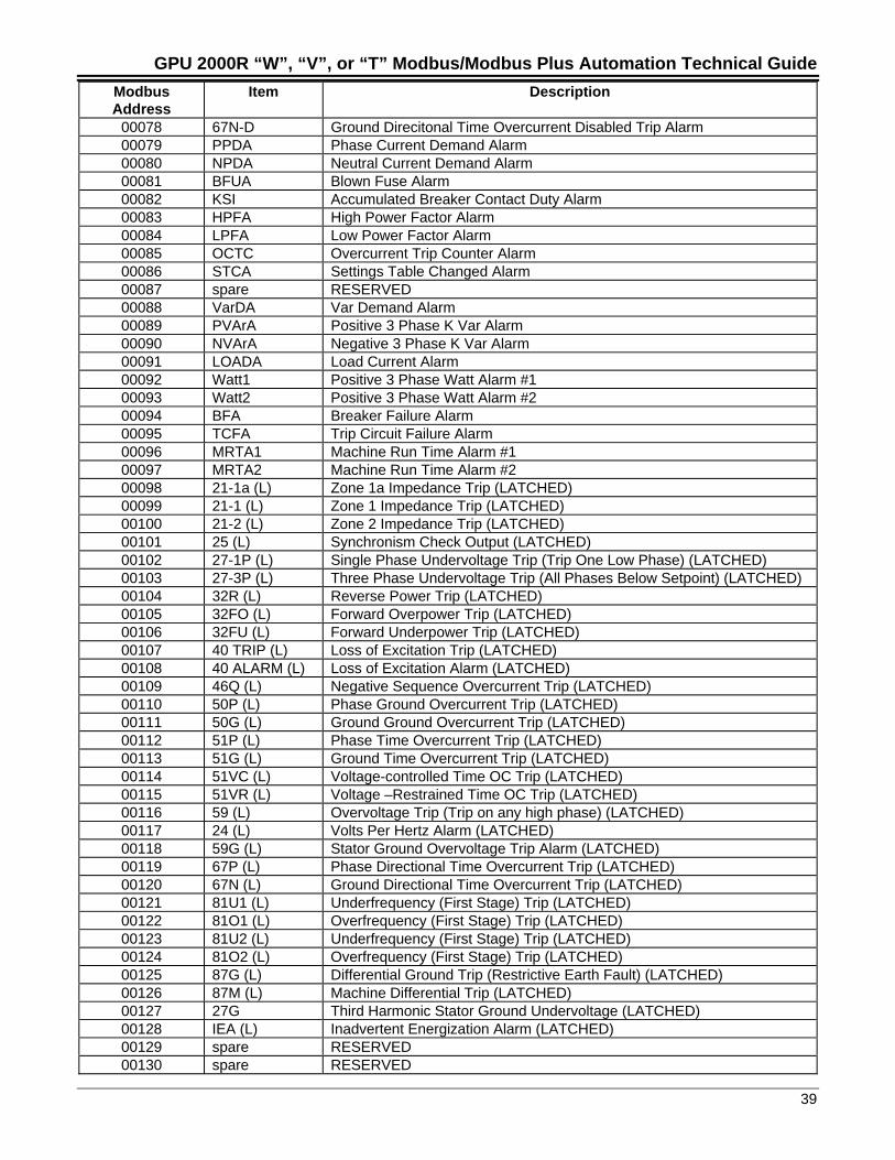
GPU 2000R “W”, “V”, or “T” Modbus/Modbus Plus Automation Technical Guide
39
ModbusAddress
Item Description
00078 67N-D Ground Direcitonal Time Overcurrent Disabled Trip Alarm00079 PPDA Phase Current Demand Alarm00080 NPDA Neutral Current Demand Alarm00081 BFUA Blown Fuse Alarm00082 KSI Accumulated Breaker Contact Duty Alarm00083 HPFA High Power Factor Alarm00084 LPFA Low Power Factor Alarm00085 OCTC Overcurrent Trip Counter Alarm00086 STCA Settings Table Changed Alarm00087 spare RESERVED00088 VarDA Var Demand Alarm00089 PVArA Positive 3 Phase K Var Alarm00090 NVArA Negative 3 Phase K Var Alarm00091 LOADA Load Current Alarm00092 Watt1 Positive 3 Phase Watt Alarm #100093 Watt2 Positive 3 Phase Watt Alarm #200094 BFA Breaker Failure Alarm00095 TCFA Trip Circuit Failure Alarm00096 MRTA1 Machine Run Time Alarm #100097 MRTA2 Machine Run Time Alarm #200098 21-1a (L) Zone 1a Impedance Trip (LATCHED)00099 21-1 (L) Zone 1 Impedance Trip (LATCHED)00100 21-2 (L) Zone 2 Impedance Trip (LATCHED)00101 25 (L) Synchronism Check Output (LATCHED)00102 27-1P (L) Single Phase Undervoltage Trip (Trip One Low Phase) (LATCHED)00103 27-3P (L) Three Phase Undervoltage Trip (All Phases Below Setpoint) (LATCHED)00104 32R (L) Reverse Power Trip (LATCHED)00105 32FO (L) Forward Overpower Trip (LATCHED)00106 32FU (L) Forward Underpower Trip (LATCHED)00107 40 TRIP (L) Loss of Excitation Trip (LATCHED)00108 40 ALARM (L) Loss of Excitation Alarm (LATCHED)00109 46Q (L) Negative Sequence Overcurrent Trip (LATCHED)00110 50P (L) Phase Ground Overcurrent Trip (LATCHED)00111 50G (L) Ground Ground Overcurrent Trip (LATCHED)00112 51P (L) Phase Time Overcurrent Trip (LATCHED)00113 51G (L) Ground Time Overcurrent Trip (LATCHED)00114 51VC (L) Voltage-controlled Time OC Trip (LATCHED)00115 51VR (L) Voltage –Restrained Time OC Trip (LATCHED)00116 59 (L) Overvoltage Trip (Trip on any high phase) (LATCHED)00117 24 (L) Volts Per Hertz Alarm (LATCHED)00118 59G (L) Stator Ground Overvoltage Trip Alarm (LATCHED)00119 67P (L) Phase Directional Time Overcurrent Trip (LATCHED)00120 67N (L) Ground Directional Time Overcurrent Trip (LATCHED)00121 81U1 (L) Underfrequency (First Stage) Trip (LATCHED)00122 81O1 (L) Overfrequency (First Stage) Trip (LATCHED)00123 81U2 (L) Underfrequency (First Stage) Trip (LATCHED)00124 81O2 (L) Overfrequency (First Stage) Trip (LATCHED)00125 87G (L) Differential Ground Trip (Restrictive Earth Fault) (LATCHED)00126 87M (L) Machine Differential Trip (LATCHED)00127 27G Third Harmonic Stator Ground Undervoltage (LATCHED)00128 IEA (L) Inadvertent Energization Alarm (LATCHED)00129 spare RESERVED00130 spare RESERVED
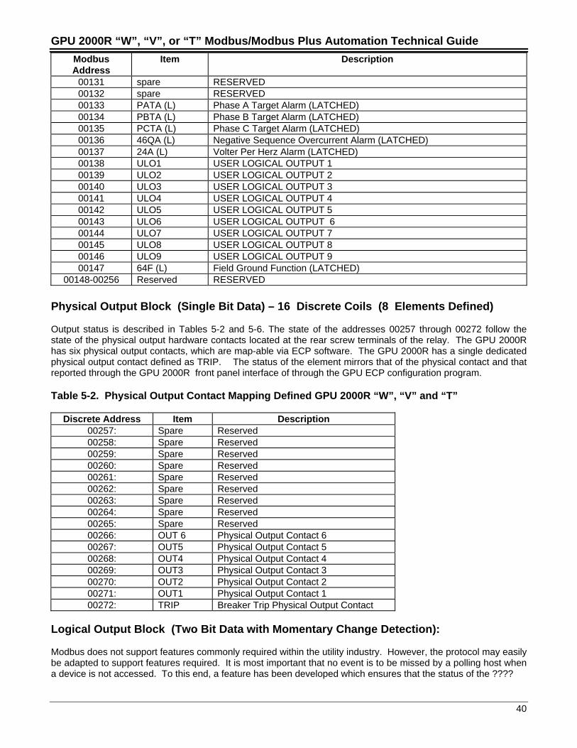
GPU 2000R “W”, “V”, or “T” Modbus/Modbus Plus Automation Technical Guide
40
ModbusAddress
Item Description
00131 spare RESERVED00132 spare RESERVED00133 PATA (L) Phase A Target Alarm (LATCHED)00134 PBTA (L) Phase B Target Alarm (LATCHED)00135 PCTA (L) Phase C Target Alarm (LATCHED)00136 46QA (L) Negative Sequence Overcurrent Alarm (LATCHED)00137 24A (L) Volter Per Herz Alarm (LATCHED)00138 ULO1 USER LOGICAL OUTPUT 100139 ULO2 USER LOGICAL OUTPUT 200140 ULO3 USER LOGICAL OUTPUT 300141 ULO4 USER LOGICAL OUTPUT 400142 ULO5 USER LOGICAL OUTPUT 500143 ULO6 USER LOGICAL OUTPUT 600144 ULO7 USER LOGICAL OUTPUT 700145 ULO8 USER LOGICAL OUTPUT 800146 ULO9 USER LOGICAL OUTPUT 900147 64F (L) Field Ground Function (LATCHED)
00148-00256 Reserved RESERVED
Physical Output Block (Single Bit Data) – 16 Discrete Coils (8 Elements Defined)
Output status is described in Tables 5-2 and 5-6. The state of the addresses 00257 through 00272 follow thestate of the physical output hardware contacts located at the rear screw terminals of the relay. The GPU 2000Rhas six physical output contacts, which are map-able via ECP software. The GPU 2000R has a single dedicatedphysical output contact defined as TRIP. The status of the element mirrors that of the physical contact and thatreported through the GPU 2000R front panel interface of through the GPU ECP configuration program.
Table 5-2. Physical Output Contact Mapping Defined GPU 2000R “W”, “V” and “T”
Discrete Address Item Description00257: Spare Reserved00258: Spare Reserved00259: Spare Reserved00260: Spare Reserved00261: Spare Reserved00262: Spare Reserved00263: Spare Reserved00264: Spare Reserved00265: Spare Reserved00266: OUT 6 Physical Output Contact 600267: OUT5 Physical Output Contact 500268: OUT4 Physical Output Contact 400269: OUT3 Physical Output Contact 300270: OUT2 Physical Output Contact 200271: OUT1 Physical Output Contact 100272: TRIP Breaker Trip Physical Output Contact
Logical Output Block (Two Bit Data with Momentary Change Detection):
Modbus does not support features commonly required within the utility industry. However, the protocol may easilybe adapted to support features required. It is most important that no event is to be missed by a polling host whena device is not accessed. To this end, a feature has been developed which ensures that the status of the ????
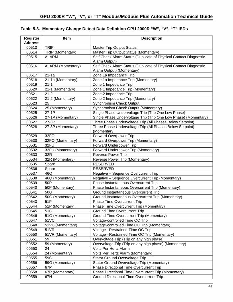
GPU 2000R “W”, “V”, or “T” Modbus/Modbus Plus Automation Technical Guide
41
Table 5-3. Momentary Change Detect Data Definition GPU 2000R “W”, “V”, “T” IEDs
RegisterAddress
Item Description
00513 TRIP Master Trip Output Status00514 TRIP (Momentary) Master Trip Output Status (Momentary)00515 ALARM Self Check Alarm Status (Duplicate of Physical Contact Diagnostic
Alarm Output)00516 ALARM (Momentary) Self Check Alarm Status (Duplicate of Physical Contact Diagnostic
Alarm Output) (Momentary)00517 21-1a Zone 1a Impedance Trip00518 21-1a (Momentary) Zone 1a Impedance Trip (Momentary)00519 21-1 Zone 1 Impedance Trip00520 21-1 (Momentary) Zone 1 Impedance Trip (Momentary)00521 21-2 Zone 2 Impedance Trip00522 21-2 (Momentary) Zone 2 Impedance Trip (Momentary)00523 25 Synchronism Check Output00524 25 (Momentary) Synchronism Check Output (Momentary)00525 27-1P Single Phase Undervoltage Trip (Trip One Low Phase)00526 27-1P (Momentary) Single Phase Undervoltage Trip (Trip One Low Phase) (Momentary)00527 27-3P Three Phase Undervoltage Trip (All Phases Below Setpoint)00528 27-3P (Momentary) Three Phase Undervoltage Trip (All Phases Below Setpoint)
(Momentary)00529 32FO Forward Overpower Trip00530 32FO (Momentary) Forward Overpower Trip (Momentary)00531 32FU Forward Underpower Trip00532 32FU (Momentary) Forward Underpower Trip (Momentary)00533 32R Reverse Power Trip00534 32R (Momentary) Reverse Power Trip (Momentary)00535 Spare RESERVED00536 Spare RESERVED00537 46Q Negative – Sequence Overcurrent Trip00538 46Q (Momentary) Negative – Sequence Overcurrent Trip (Momentary)00539 50P Phase Instantaneous Overcurrent Trip00540 50P (Momentary) Phase Instantaneous Overcurrent Trip (Momentary)00541 50G Ground Instantaneous Overcurrent Trip00542 50G (Momentary) Ground Instantaneous Overcurrent Trip (Momentary)00543 51P Phase Time Overcurrent Trip00544 51P (Momentary) Phase Time Overcurrent Trip (Momentary)00545 51G Ground Time Overcurrent Trip00546 51G (Momentary) Ground Time Overcurrent Trip (Momentary)00547 51VC Voltage-controlled Time OC Trip00548 51VC (Momentary) Voltage-controlled Time OC Trip (Momentary)00549 51VR Voltage –Restrained Time OC Trip00550 51VR (Momentary) Voltage –Restrained Time OC Trip (Momentary)00551 59 Overvoltage Trip (Trip on any high phase)00552 59 (Momentary) Overvoltage Trip (Trip on any high phase) (Momentary)00553 24 Volts Per Hertz Alarm00554 24 (Momentary) Volts Per Hertz Alarm (Momentary)00555 59G Stator Ground Overvoltage Trip00556 59G (Momentary) Stator Ground Overvoltage Trip (Momentary)00557 67P Phase Directional Time Overcurrent Trip00558 67P (Momentary) Phase Directional Time Overcurrent Trip (Momentary)00559 67N Ground Directional Time Overcurrent Trip
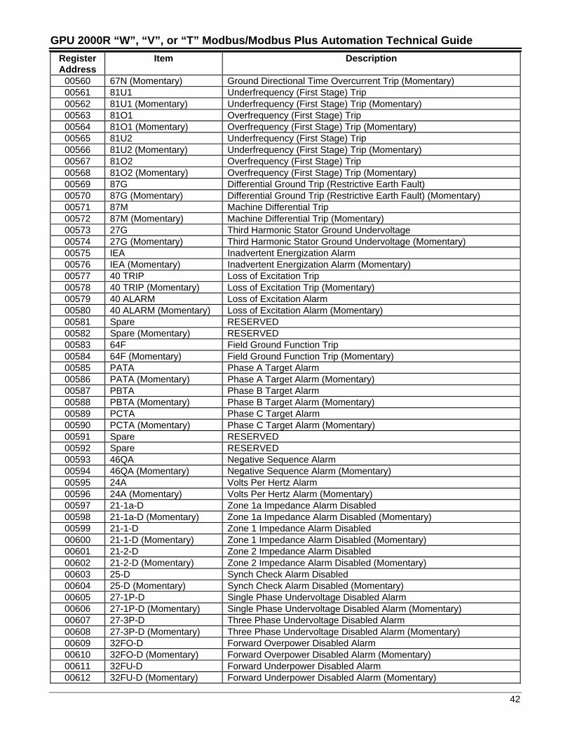
GPU 2000R “W”, “V”, or “T” Modbus/Modbus Plus Automation Technical Guide
42
RegisterAddress
Item Description
00560 67N (Momentary) Ground Directional Time Overcurrent Trip (Momentary)00561 81U1 Underfrequency (First Stage) Trip00562 81U1 (Momentary) Underfrequency (First Stage) Trip (Momentary)00563 81O1 Overfrequency (First Stage) Trip00564 81O1 (Momentary) Overfrequency (First Stage) Trip (Momentary)00565 81U2 Underfrequency (First Stage) Trip00566 81U2 (Momentary) Underfrequency (First Stage) Trip (Momentary)00567 81O2 Overfrequency (First Stage) Trip00568 81O2 (Momentary) Overfrequency (First Stage) Trip (Momentary)00569 87G Differential Ground Trip (Restrictive Earth Fault)00570 87G (Momentary) Differential Ground Trip (Restrictive Earth Fault) (Momentary)00571 87M Machine Differential Trip00572 87M (Momentary) Machine Differential Trip (Momentary)00573 27G Third Harmonic Stator Ground Undervoltage00574 27G (Momentary) Third Harmonic Stator Ground Undervoltage (Momentary)00575 IEA Inadvertent Energization Alarm00576 IEA (Momentary) Inadvertent Energization Alarm (Momentary)00577 40 TRIP Loss of Excitation Trip00578 40 TRIP (Momentary) Loss of Excitation Trip (Momentary)00579 40 ALARM Loss of Excitation Alarm00580 40 ALARM (Momentary) Loss of Excitation Alarm (Momentary)00581 Spare RESERVED00582 Spare (Momentary) RESERVED00583 64F Field Ground Function Trip00584 64F (Momentary) Field Ground Function Trip (Momentary)00585 PATA Phase A Target Alarm00586 PATA (Momentary) Phase A Target Alarm (Momentary)00587 PBTA Phase B Target Alarm00588 PBTA (Momentary) Phase B Target Alarm (Momentary)00589 PCTA Phase C Target Alarm00590 PCTA (Momentary) Phase C Target Alarm (Momentary)00591 Spare RESERVED00592 Spare RESERVED00593 46QA Negative Sequence Alarm00594 46QA (Momentary) Negative Sequence Alarm (Momentary)00595 24A Volts Per Hertz Alarm00596 24A (Momentary) Volts Per Hertz Alarm (Momentary)00597 21-1a-D Zone 1a Impedance Alarm Disabled00598 21-1a-D (Momentary) Zone 1a Impedance Alarm Disabled (Momentary)00599 21-1-D Zone 1 Impedance Alarm Disabled00600 21-1-D (Momentary) Zone 1 Impedance Alarm Disabled (Momentary)00601 21-2-D Zone 2 Impedance Alarm Disabled00602 21-2-D (Momentary) Zone 2 Impedance Alarm Disabled (Momentary)00603 25-D Synch Check Alarm Disabled00604 25-D (Momentary) Synch Check Alarm Disabled (Momentary)00605 27-1P-D Single Phase Undervoltage Disabled Alarm00606 27-1P-D (Momentary) Single Phase Undervoltage Disabled Alarm (Momentary)00607 27-3P-D Three Phase Undervoltage Disabled Alarm00608 27-3P-D (Momentary) Three Phase Undervoltage Disabled Alarm (Momentary)00609 32FO-D Forward Overpower Disabled Alarm00610 32FO-D (Momentary) Forward Overpower Disabled Alarm (Momentary)00611 32FU-D Forward Underpower Disabled Alarm00612 32FU-D (Momentary) Forward Underpower Disabled Alarm (Momentary)
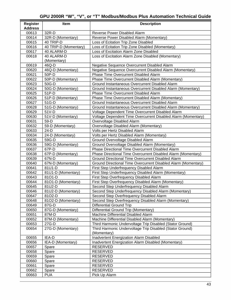
GPU 2000R “W”, “V”, or “T” Modbus/Modbus Plus Automation Technical Guide
43
RegisterAddress
Item Description
00613 32R-D Reverse Power Disabled Alarm00614 32R-D (Momentary) Reverse Power Disabled Alarm (Momentary)00615 40 TRIP-D Loss of Ecitation Trip Zone Disabled00616 40 TRIP-D (Momentary) Loss of Ecitation Trip Zone Disabled (Momentary)00617 40 ALARM-D Loss of Excitation Alarm Zone Disabled00618 40 ALARM-D
(Momentary)Loss of Excitation Alarm Zone Disabled (Momentary)
00619 46Q-D Negative Sequence Overcurrent Disabled Alarm00620 46Q-D (Momentary) Negative Sequence Overcurrent Disabled Alarm (Momentary)00621 50P-D Phase Time Overcurrent Disabled Alarm00622 50P-D (Momentary) Phase Time Overcurrent Disabled Alarm (Momentary)00623 50G-D Ground Instantaneous Overcurrent Disabled Alarm00624 50G-D (Momentary) Ground Instantaneous Overcurrent Disabled Alarm (Momentary)00625 51P-D Phase Time Overcurrent Disabled Alarm00626 51P-D (Momentary) Phase Time Overcurrent Disabled Alarm (Momentary)00627 51G-D Ground Instantaneous Overcurrent Disabled Alarm00628 51G-D (Momentary) Ground Instantaneous Overcurrent Disabled Alarm (Momentary)00629 51V-D Voltage Dependent Time Overcurrent Disabled Alarm00630 51V-D (Momentary) Voltage Dependent Time Overcurrent Disabled Alarm (Momentary)00631 59-D Overvoltage Disabled Alarm00632 59-D (Momentary) Overvoltage Disabled Alarm (Momentary)00633 24-D Volts per Hertz Disabled Alarm00634 24-D (Momentary) Volts per Hertz Disabled Alarm (Momentary)00635 59G-D Ground Overvoltage Disabled Alarm00636 59G-D (Momentary) Ground Overvoltage Disabled Alarm (Momentary)00637 67P-D Phase Directional Time Overcurrent Disabled Alarm00638 67P-D (Momentary) Phase Directional Time Overcurrent Disabled Alarm (Momentary)00639 67N-D Ground Directional Time Overcurrent Disabled Alarm00640 67N-D (Momentary) Ground Directional Time Overcurrent Disabled Alarm (Momentary)00641 81U1-D First Step Underfrequency Disabled Alarm00642 81U1-D (Momentary) First Step Underfrequency Disabled Alarm (Momentary)00643 81O1-D First Step Overfrequency Disabled Alarm00644 81O1-D (Momentary) First Step Overfrequency Disabled Alarm (Momentary)00645 81U2-D Second Step Underfrequency Disabled Alarm00646 81U2-D (Momentary) Second Step Underfrequency Disabled Alarm (Momentary)00647 81O2-D Second Step Overfrequency Disabled Alarm00648 81O2-D (Momentary) Second Step Overfrequency Disabled Alarm (Momentary)00649 87G-D Differential Ground Trip00650 87G-D (Momentary) Differential Ground Trip (Momentary)00651 87M-D Machine Differential Disabled Alarm00652 87M-D (Momentary) Machine Differential Disabled Alarm (Momentary)00653 27G-D Third Harmonic Undervoltage Trip Disabled (Stator Ground)00654 27G-D (Momentary) Third Harmonic Undervoltage Trip Disabled (Stator Ground)
(Momentary)00655 IEA-D Inadvertent Energization Alarm Disabled00656 IEA-D (Momentary) Inadvertent Energization Alarm Disabled (Momentary)00657 Spare RESERVED00658 Spare RESERVED00659 Spare RESERVED00660 Spare RESERVED00661 Spare RESERVED00662 Spare RESERVED00663 PUA Pick Up Alarm
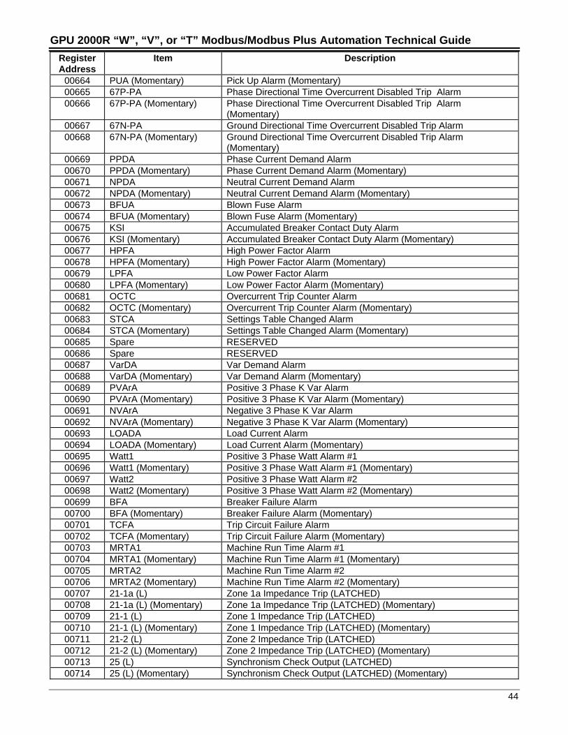
GPU 2000R “W”, “V”, or “T” Modbus/Modbus Plus Automation Technical Guide
44
RegisterAddress
Item Description
00664 PUA (Momentary) Pick Up Alarm (Momentary)00665 67P-PA Phase Directional Time Overcurrent Disabled Trip Alarm00666 67P-PA (Momentary) Phase Directional Time Overcurrent Disabled Trip Alarm
(Momentary)00667 67N-PA Ground Directional Time Overcurrent Disabled Trip Alarm00668 67N-PA (Momentary) Ground Directional Time Overcurrent Disabled Trip Alarm
(Momentary)00669 PPDA Phase Current Demand Alarm00670 PPDA (Momentary) Phase Current Demand Alarm (Momentary)00671 NPDA Neutral Current Demand Alarm00672 NPDA (Momentary) Neutral Current Demand Alarm (Momentary)00673 BFUA Blown Fuse Alarm00674 BFUA (Momentary) Blown Fuse Alarm (Momentary)00675 KSI Accumulated Breaker Contact Duty Alarm00676 KSI (Momentary) Accumulated Breaker Contact Duty Alarm (Momentary)00677 HPFA High Power Factor Alarm00678 HPFA (Momentary) High Power Factor Alarm (Momentary)00679 LPFA Low Power Factor Alarm00680 LPFA (Momentary) Low Power Factor Alarm (Momentary)00681 OCTC Overcurrent Trip Counter Alarm00682 OCTC (Momentary) Overcurrent Trip Counter Alarm (Momentary)00683 STCA Settings Table Changed Alarm00684 STCA (Momentary) Settings Table Changed Alarm (Momentary)00685 Spare RESERVED00686 Spare RESERVED00687 VarDA Var Demand Alarm00688 VarDA (Momentary) Var Demand Alarm (Momentary)00689 PVArA Positive 3 Phase K Var Alarm00690 PVArA (Momentary) Positive 3 Phase K Var Alarm (Momentary)00691 NVArA Negative 3 Phase K Var Alarm00692 NVArA (Momentary) Negative 3 Phase K Var Alarm (Momentary)00693 LOADA Load Current Alarm00694 LOADA (Momentary) Load Current Alarm (Momentary)00695 Watt1 Positive 3 Phase Watt Alarm #100696 Watt1 (Momentary) Positive 3 Phase Watt Alarm #1 (Momentary)00697 Watt2 Positive 3 Phase Watt Alarm #200698 Watt2 (Momentary) Positive 3 Phase Watt Alarm #2 (Momentary)00699 BFA Breaker Failure Alarm00700 BFA (Momentary) Breaker Failure Alarm (Momentary)00701 TCFA Trip Circuit Failure Alarm00702 TCFA (Momentary) Trip Circuit Failure Alarm (Momentary)00703 MRTA1 Machine Run Time Alarm #100704 MRTA1 (Momentary) Machine Run Time Alarm #1 (Momentary)00705 MRTA2 Machine Run Time Alarm #200706 MRTA2 (Momentary) Machine Run Time Alarm #2 (Momentary)00707 21-1a (L) Zone 1a Impedance Trip (LATCHED)00708 21-1a (L) (Momentary) Zone 1a Impedance Trip (LATCHED) (Momentary)00709 21-1 (L) Zone 1 Impedance Trip (LATCHED)00710 21-1 (L) (Momentary) Zone 1 Impedance Trip (LATCHED) (Momentary)00711 21-2 (L) Zone 2 Impedance Trip (LATCHED)00712 21-2 (L) (Momentary) Zone 2 Impedance Trip (LATCHED) (Momentary)00713 25 (L) Synchronism Check Output (LATCHED)00714 25 (L) (Momentary) Synchronism Check Output (LATCHED) (Momentary)
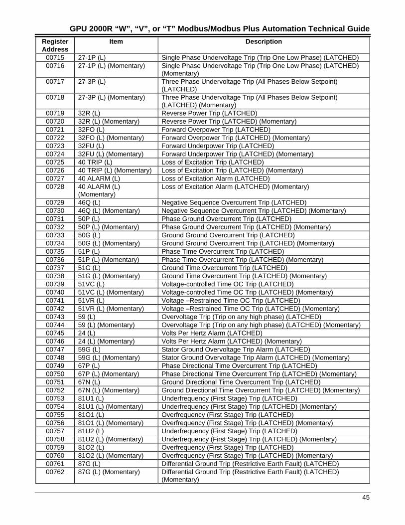
GPU 2000R “W”, “V”, or “T” Modbus/Modbus Plus Automation Technical Guide
45
RegisterAddress
Item Description
00715 27-1P (L) Single Phase Undervoltage Trip (Trip One Low Phase) (LATCHED)00716 27-1P (L) (Momentary) Single Phase Undervoltage Trip (Trip One Low Phase) (LATCHED)
(Momentary)00717 27-3P (L) Three Phase Undervoltage Trip (All Phases Below Setpoint)
(LATCHED)00718 27-3P (L) (Momentary) Three Phase Undervoltage Trip (All Phases Below Setpoint)
(LATCHED) (Momentary)00719 32R (L) Reverse Power Trip (LATCHED)00720 32R (L) (Momentary) Reverse Power Trip (LATCHED) (Momentary)00721 32FO (L) Forward Overpower Trip (LATCHED)00722 32FO (L) (Momentary) Forward Overpower Trip (LATCHED) (Momentary)00723 32FU (L) Forward Underpower Trip (LATCHED)00724 32FU (L) (Momentary) Forward Underpower Trip (LATCHED) (Momentary)00725 40 TRIP (L) Loss of Excitation Trip (LATCHED)00726 40 TRIP (L) (Momentary) Loss of Excitation Trip (LATCHED) (Momentary)00727 40 ALARM (L) Loss of Excitation Alarm (LATCHED)00728 40 ALARM (L)
(Momentary)Loss of Excitation Alarm (LATCHED) (Momentary)
00729 46Q (L) Negative Sequence Overcurrent Trip (LATCHED)00730 46Q (L) (Momentary) Negative Sequence Overcurrent Trip (LATCHED) (Momentary)00731 50P (L) Phase Ground Overcurrent Trip (LATCHED)00732 50P (L) (Momentary) Phase Ground Overcurrent Trip (LATCHED) (Momentary)00733 50G (L) Ground Ground Overcurrent Trip (LATCHED)00734 50G (L) (Momentary) Ground Ground Overcurrent Trip (LATCHED) (Momentary)00735 51P (L) Phase Time Overcurrent Trip (LATCHED)00736 51P (L) (Momentary) Phase Time Overcurrent Trip (LATCHED) (Momentary)00737 51G (L) Ground Time Overcurrent Trip (LATCHED)00738 51G (L) (Momentary) Ground Time Overcurrent Trip (LATCHED) (Momentary)00739 51VC (L) Voltage-controlled Time OC Trip (LATCHED)00740 51VC (L) (Momentary) Voltage-controlled Time OC Trip (LATCHED) (Momentary)00741 51VR (L) Voltage –Restrained Time OC Trip (LATCHED)00742 51VR (L) (Momentary) Voltage –Restrained Time OC Trip (LATCHED) (Momentary)00743 59 (L) Overvoltage Trip (Trip on any high phase) (LATCHED)00744 59 (L) (Momentary) Overvoltage Trip (Trip on any high phase) (LATCHED) (Momentary)00745 24 (L) Volts Per Hertz Alarm (LATCHED)00746 24 (L) (Momentary) Volts Per Hertz Alarm (LATCHED) (Momentary)00747 59G (L) Stator Ground Overvoltage Trip Alarm (LATCHED)00748 59G (L) (Momentary) Stator Ground Overvoltage Trip Alarm (LATCHED) (Momentary)00749 67P (L) Phase Directional Time Overcurrent Trip (LATCHED)00750 67P (L) (Momentary) Phase Directional Time Overcurrent Trip (LATCHED) (Momentary)00751 67N (L) Ground Directional Time Overcurrent Trip (LATCHED)00752 67N (L) (Momentary) Ground Directional Time Overcurrent Trip (LATCHED) (Momentary)00753 81U1 (L) Underfrequency (First Stage) Trip (LATCHED)00754 81U1 (L) (Momentary) Underfrequency (First Stage) Trip (LATCHED) (Momentary)00755 81O1 (L) Overfrequency (First Stage) Trip (LATCHED)00756 81O1 (L) (Momentary) Overfrequency (First Stage) Trip (LATCHED) (Momentary)00757 81U2 (L) Underfrequency (First Stage) Trip (LATCHED)00758 81U2 (L) (Momentary) Underfrequency (First Stage) Trip (LATCHED) (Momentary)00759 81O2 (L) Overfrequency (First Stage) Trip (LATCHED)00760 81O2 (L) (Momentary) Overfrequency (First Stage) Trip (LATCHED) (Momentary)00761 87G (L) Differential Ground Trip (Restrictive Earth Fault) (LATCHED)00762 87G (L) (Momentary) Differential Ground Trip (Restrictive Earth Fault) (LATCHED)
(Momentary)
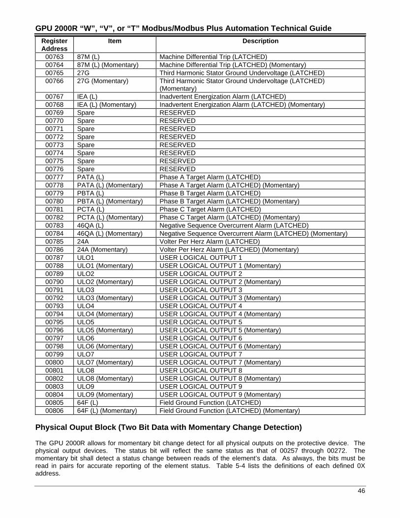
GPU 2000R “W”, “V”, or “T” Modbus/Modbus Plus Automation Technical Guide
46
RegisterAddress
Item Description
00763 87M (L) Machine Differential Trip (LATCHED)00764 87M (L) (Momentary) Machine Differential Trip (LATCHED) (Momentary)00765 27G Third Harmonic Stator Ground Undervoltage (LATCHED)00766 27G (Momentary) Third Harmonic Stator Ground Undervoltage (LATCHED)
(Momentary)00767 IEA (L) Inadvertent Energization Alarm (LATCHED)00768 IEA (L) (Momentary) Inadvertent Energization Alarm (LATCHED) (Momentary)00769 Spare RESERVED00770 Spare RESERVED00771 Spare RESERVED00772 Spare RESERVED00773 Spare RESERVED00774 Spare RESERVED00775 Spare RESERVED00776 Spare RESERVED00777 PATA (L) Phase A Target Alarm (LATCHED)00778 PATA (L) (Momentary) Phase A Target Alarm (LATCHED) (Momentary)00779 PBTA (L) Phase B Target Alarm (LATCHED)00780 PBTA (L) (Momentary) Phase B Target Alarm (LATCHED) (Momentary)00781 PCTA (L) Phase C Target Alarm (LATCHED)00782 PCTA (L) (Momentary) Phase C Target Alarm (LATCHED) (Momentary)00783 46QA (L) Negative Sequence Overcurrent Alarm (LATCHED)00784 46QA (L) (Momentary) Negative Sequence Overcurrent Alarm (LATCHED) (Momentary)00785 24A Volter Per Herz Alarm (LATCHED)00786 24A (Momentary) Volter Per Herz Alarm (LATCHED) (Momentary)00787 ULO1 USER LOGICAL OUTPUT 100788 ULO1 (Momentary) USER LOGICAL OUTPUT 1 (Momentary)00789 ULO2 USER LOGICAL OUTPUT 200790 ULO2 (Momentary) USER LOGICAL OUTPUT 2 (Momentary)00791 ULO3 USER LOGICAL OUTPUT 300792 ULO3 (Momentary) USER LOGICAL OUTPUT 3 (Momentary)00793 ULO4 USER LOGICAL OUTPUT 400794 ULO4 (Momentary) USER LOGICAL OUTPUT 4 (Momentary)00795 ULO5 USER LOGICAL OUTPUT 500796 ULO5 (Momentary) USER LOGICAL OUTPUT 5 (Momentary)00797 ULO6 USER LOGICAL OUTPUT 600798 ULO6 (Momentary) USER LOGICAL OUTPUT 6 (Momentary)00799 ULO7 USER LOGICAL OUTPUT 700800 ULO7 (Momentary) USER LOGICAL OUTPUT 7 (Momentary)00801 ULO8 USER LOGICAL OUTPUT 800802 ULO8 (Momentary) USER LOGICAL OUTPUT 8 (Momentary)00803 ULO9 USER LOGICAL OUTPUT 900804 ULO9 (Momentary) USER LOGICAL OUTPUT 9 (Momentary)00805 64F (L) Field Ground Function (LATCHED)00806 64F (L) (Momentary) Field Ground Function (LATCHED) (Momentary)
Physical Ouput Block (Two Bit Data with Momentary Change Detection)
The GPU 2000R allows for momentary bit change detect for all physical outputs on the protective device. Thephysical output devices. The status bit will reflect the same status as that of 00257 through 00272. Themomentary bit shall detect a status change between reads of the element’s data. As always, the bits must beread in pairs for accurate reporting of the element status. Table 5-4 lists the definitions of each defined 0Xaddress.
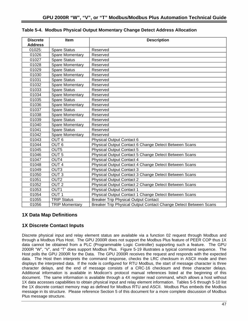
GPU 2000R “W”, “V”, or “T” Modbus/Modbus Plus Automation Technical Guide
47
Table 5-4. Modbus Physical Output Momentary Change Detect Address Allocation
DiscreteAddress
Item Description
01025: Spare Status Reserved01026 Spare Momentary Reserved01027 Spare Status Reserved01028 Spare Momentary Reserved01029 Spare Status Reserved01030 Spare Momentary Reserved01031 Spare Status Reserved01032 Spare Momentary Reserved01033 Spare Status Reserved01034 Spare Momentary Reserved01035 Spare Status Reserved01036 Spare Momentary Reserved01037 Spare Status Reserved01038 Spare Momentary Reserved01039 Spare Status Reserved01040 Spare Momentary Reserved01041 Spare Status Reserved01042 Spare Momentary Reserved01043 OUT 6 Physical Output Contact 601044 OUT 6 Physical Output Contact 6 Change Detect Between Scans01045 OUT5 Physical Output Contact 501046 OUT 5 Physical Output Contact 5 Change Detect Between Scans01047 OUT4 Physical Output Contact 401048 OUT 4 Physical Output Contact 4 Change Detect Between Scans01049 OUT3 Physical Output Contact 301050 OUT 3 Physical Output Contact 3 Change Detect Between Scans01051 OUT2 Physical Output Contact 201052 OUT 2 Physical Output Contact 2 Change Detect Between Scans01053 OUT1 Physical Output Contact 101054 OUT 1 Physical Output Contact 1 Change Detect Between Scans01055 TRIP Status Breaker Trip Physical Output Contact01056 TRIP Momentary Breaker Trip Physical Output Contact Change Detect Between Scans
1X Data Map Definitions
1X Discrete Contact Inputs
Discrete physical input and relay element status are available via a function 02 request through Modbus andthrough a Modbus Plus Host. The GPU 2000R does not support the Modbus Plus feature of PEER COP thus 1Xdata cannot be obtained from a PLC (Programmable Logic Controller) supporting such a feature. The GPU2000R “W”, “V”, and “T” does support Modbus Plus. Figure 5-19 illustrates a typical command sequence. TheHost polls the GPU 2000R for the Data. The GPU 2000R receives the request and responds with the expecteddata. The Host then interprets the command response, checks the LRC checksum in ASCII mode and thendisplays the interpreted data. If the node is configured for RTU Modbus, the start of message character is threecharacter delays, and the end of message consists of a CRC-16 checksum and three character delays.Additional information is available in Modicon’s protocol manual references listed at the beginning of thisdocument. The same information is available through a 4X register read command, which allows a host without1X data accesses capabilities to obtain physical input and relay element information. Tables 5-5 through 5-10 listthe 1X discrete contact memory map as defined for Modbus RTU and ASCII. Modbus Plus embeds the Modbusmessage in its structure. Please reference Section 5 of this document for a more complete discussion of ModbusPlus message structure.
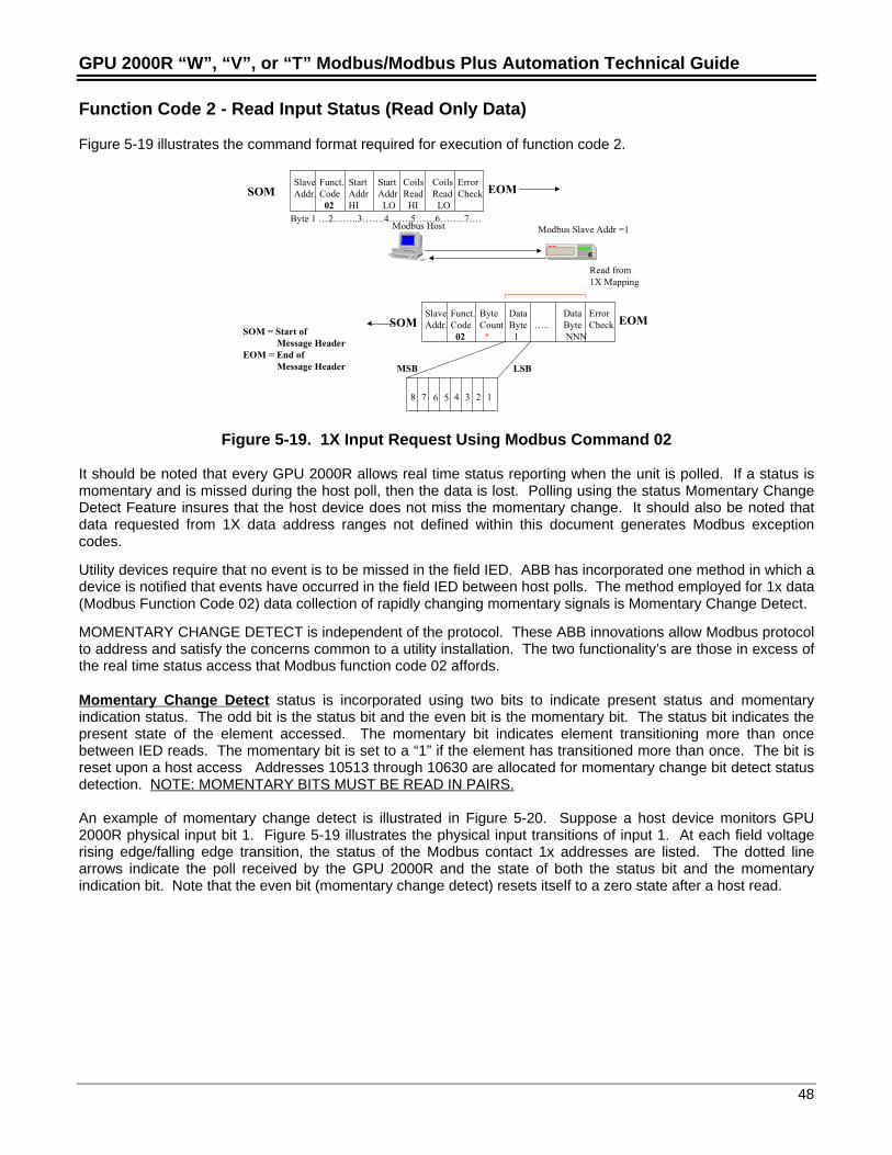
GPU 2000R “W”, “V”, or “T” Modbus/Modbus Plus Automation Technical Guide
48
Function Code 2 - Read Input Status (Read Only Data)
Figure 5-19 illustrates the command format required for execution of function code 2.
Modbus Host Modbus Slave Addr =1
Read from 1X Mapping
SlaveAddr.
Funct.Code 02
StartAddrHI
Start Addr LO
CoilsRead HI
CoilsRead LO
ErrorCheck EOMSOM
SlaveAddr.
Funct.Code 02
ByteCount *
DataByte 1
…..DataByte NNN
ErrorCheck EOMSOM
Byte 1 …2……..3…….4…….5……6……..7….
MSB LSB
8 7 6 5 4 3 2 1
SOM = Start of Message HeaderEOM = End of Message Header
EC
Figure 5-19. 1X Input Request Using Modbus Command 02
It should be noted that every GPU 2000R allows real time status reporting when the unit is polled. If a status ismomentary and is missed during the host poll, then the data is lost. Polling using the status Momentary ChangeDetect Feature insures that the host device does not miss the momentary change. It should also be noted thatdata requested from 1X data address ranges not defined within this document generates Modbus exceptioncodes.
Utility devices require that no event is to be missed in the field IED. ABB has incorporated one method in which adevice is notified that events have occurred in the field IED between host polls. The method employed for 1x data(Modbus Function Code 02) data collection of rapidly changing momentary signals is Momentary Change Detect.
MOMENTARY CHANGE DETECT is independent of the protocol. These ABB innovations allow Modbus protocolto address and satisfy the concerns common to a utility installation. The two functionality’s are those in excess ofthe real time status access that Modbus function code 02 affords.
Momentary Change Detect status is incorporated using two bits to indicate present status and momentaryindication status. The odd bit is the status bit and the even bit is the momentary bit. The status bit indicates thepresent state of the element accessed. The momentary bit indicates element transitioning more than oncebetween IED reads. The momentary bit is set to a “1” if the element has transitioned more than once. The bit isreset upon a host access Addresses 10513 through 10630 are allocated for momentary change bit detect statusdetection. NOTE: MOMENTARY BITS MUST BE READ IN PAIRS.
An example of momentary change detect is illustrated in Figure 5-20. Suppose a host device monitors GPU2000R physical input bit 1. Figure 5-19 illustrates the physical input transitions of input 1. At each field voltagerising edge/falling edge transition, the status of the Modbus contact 1x addresses are listed. The dotted linearrows indicate the poll received by the GPU 2000R and the state of both the status bit and the momentaryindication bit. Note that the even bit (momentary change detect) resets itself to a zero state after a host read.
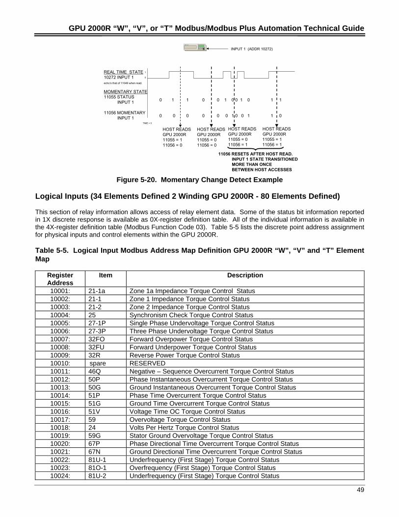
GPU 2000R “W”, “V”, or “T” Modbus/Modbus Plus Automation Technical Guide
49
EC INPUT 1 (ADDR 10272)
REAL TIME STATE10272 INPUT 1echo’s that of 11049 when read.
1
0
MOMENTARY STATE11055 STATUS INPUT 1
11056 MOMENTARY INPUT 1
TIME = 0
0 1 1 0 0 1 0 0 1 0 1 1
0 0 0 0 0 0 1 0 0 1 1 0
HOST READSGPU 2000R11055 = 111056 = 0
HOST READSGPU 2000R11055 = 011056 = 0
HOST READS HOST READSGPU 2000R GPU 2000R11055 = 0 11055 = 111056 = 1 11056 = 1
11056 RESETS AFTER HOST READ. INPUT 1 STATE TRANSITIONED
MORE THAN ONCE BETWEEN HOST ACCESSES
Figure 5-20. Momentary Change Detect Example
Logical Inputs (34 Elements Defined 2 Winding GPU 2000R - 80 Elements Defined)
This section of relay information allows access of relay element data. Some of the status bit information reportedin 1X discrete response is available as 0X-register definition table. All of the individual information is available inthe 4X-register definition table (Modbus Function Code 03). Table 5-5 lists the discrete point address assignmentfor physical inputs and control elements within the GPU 2000R.
Table 5-5. Logical Input Modbus Address Map Definition GPU 2000R “W”, “V” and “T” ElementMap
RegisterAddress
Item Description
10001: 21-1a Zone 1a Impedance Torque Control Status10002: 21-1 Zone 1 Impedance Torque Control Status10003: 21-2 Zone 2 Impedance Torque Control Status10004: 25 Synchronism Check Torque Control Status10005: 27-1P Single Phase Undervoltage Torque Control Status10006: 27-3P Three Phase Undervoltage Torque Control Status10007: 32FO Forward Overpower Torque Control Status10008: 32FU Forward Underpower Torque Control Status10009: 32R Reverse Power Torque Control Status10010: spare RESERVED10011: 46Q Negative – Sequence Overcurrent Torque Control Status10012: 50P Phase Instantaneous Overcurrent Torque Control Status10013: 50G Ground Instantaneous Overcurrent Torque Control Status10014: 51P Phase Time Overcurrent Torque Control Status10015: 51G Ground Time Overcurrent Torque Control Status10016: 51V Voltage Time OC Torque Control Status10017: 59 Overvoltage Torque Control Status10018: 24 Volts Per Hertz Torque Control Status10019: 59G Stator Ground Overvoltage Torque Control Status10020: 67P Phase Directional Time Overcurrent Torque Control Status10021: 67N Ground Directional Time Overcurrent Torque Control Status10022: 81U-1 Underfrequency (First Stage) Torque Control Status10023: 81O-1 Overfrequency (First Stage) Torque Control Status10024: 81U-2 Underfrequency (First Stage) Torque Control Status
GPU 2000R “W”, “V”, or “T” Modbus/Modbus Plus Automation Technical Guide
50
RegisterAddress
Item Description
10025: 81O-2 Overfrequency (First Stage) Torque Control Status10026: 87G Differential Ground Trip (Restrictive Earth Fault) Torque Control Status10027: 87M Machine Differential Torque Control Status10028: 27G Third Harmonic Stator Ground Undervoltage Torque Control Status10029: 24A Volts Per Hertz Alarm Torque Control Status10030: 46Q Negative Sequence Overcurrent Instantaneous Thermal Memory Reset Status10031: 40 TRIP Loss of Excitation Torque Control – Zone 1 (Trip) Status10032: 40 ALARM Loss of Excitiation Torque Control – Zone 2 (Alarm) Status10033: 52A Breaker Status10034: spare RESERVED10035: M Trip Coil Monitoring Status10036: ALT1 Alternate Settings 1 Status10037: ALT2 Alternate Settings 2 Status10038: ECI1 Event Capture 1 Initated10040: ECI2 Event Capture 2 Initiated10041: WCI Waveform Capture Initated10042: OPEN External Trip Initiated10043: spare RESERVED10044: CRI Overcurrent and Differential Trip Counters Reset10045: spare RESERVED10046: spare RESERVED10047: spare RESERVED10048: spare RESERVED10049: spare RESERVED10050: ULI1 USER LOGICAL INPUT 1 Status10051: ULI2 USER LOGICAL INPUT 2 Status10052: ULI3 USER LOGICAL INPUT 3 Status10053: ULI4 USER LOGICAL INPUT 4 Status10054: ULI5 USER LOGICAL INPUT 5 Status10055: ULI6 USER LOGICAL INPUT 6 Status10056: ULI7 USER LOGICAL INPUT 7 Status10057: ULI8 USER LOGICAL INPUT 8 Status10058: ULI9 USER LOGICAL INPUT 9 Status10059: CLTRGT Clear Target Status10060: CLSEAL Clear Seal In Element Status10061: 64F Field Ground Input from External Relay Status10062: Blown Fuse Blown Fuse Indication Status10063: spare RESERVED10064: spare RESERVED10065: spare RESERVED10066: spare RESERVED10067: spare RESERVED10068: spare RESERVED10069: spare RESERVED10070: spare RESERVED10071: IEA Inadvertent Engergization Torque Control Status10072: UDI User Defined Message Display Initiated10073:
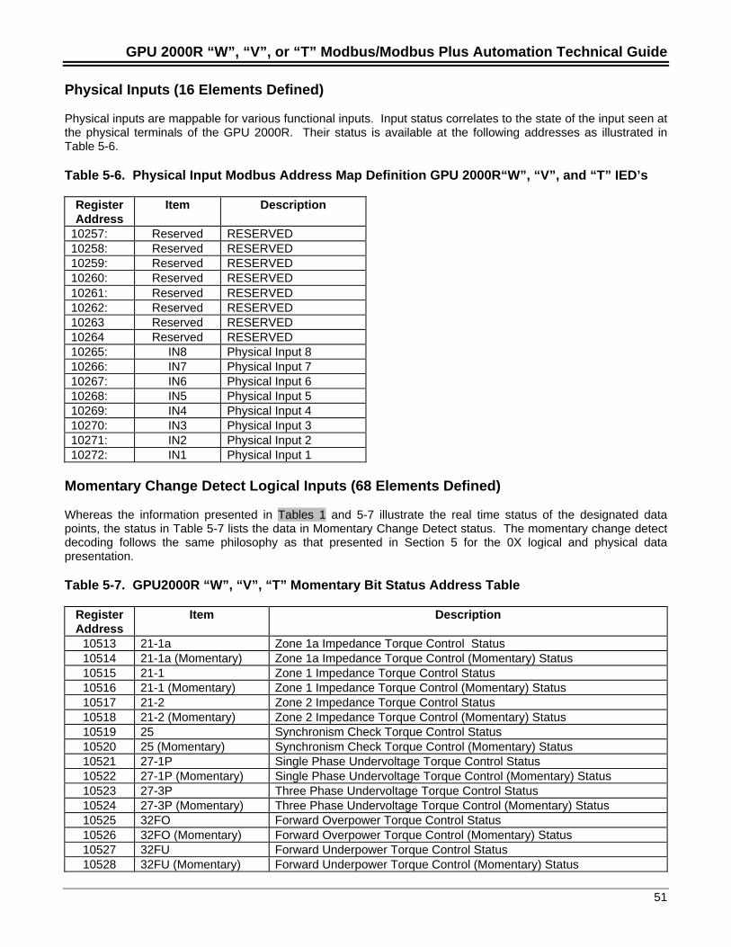
GPU 2000R “W”, “V”, or “T” Modbus/Modbus Plus Automation Technical Guide
51
Physical Inputs (16 Elements Defined)
Physical inputs are mappable for various functional inputs. Input status correlates to the state of the input seen atthe physical terminals of the GPU 2000R. Their status is available at the following addresses as illustrated inTable 5-6.
Table 5-6. Physical Input Modbus Address Map Definition GPU 2000R“W”, “V”, and “T” IED’s
RegisterAddress
Item Description
10257: Reserved RESERVED10258: Reserved RESERVED10259: Reserved RESERVED10260: Reserved RESERVED10261: Reserved RESERVED10262: Reserved RESERVED10263 Reserved RESERVED10264 Reserved RESERVED10265: IN8 Physical Input 810266: IN7 Physical Input 710267: IN6 Physical Input 610268: IN5 Physical Input 510269: IN4 Physical Input 410270: IN3 Physical Input 310271: IN2 Physical Input 210272: IN1 Physical Input 1
Momentary Change Detect Logical Inputs (68 Elements Defined)
Whereas the information presented in Tables 1 and 5-7 illustrate the real time status of the designated datapoints, the status in Table 5-7 lists the data in Momentary Change Detect status. The momentary change detectdecoding follows the same philosophy as that presented in Section 5 for the 0X logical and physical datapresentation.
Table 5-7. GPU2000R “W”, “V”, “T” Momentary Bit Status Address Table
RegisterAddress
Item Description
10513 21-1a Zone 1a Impedance Torque Control Status10514 21-1a (Momentary) Zone 1a Impedance Torque Control (Momentary) Status10515 21-1 Zone 1 Impedance Torque Control Status10516 21-1 (Momentary) Zone 1 Impedance Torque Control (Momentary) Status10517 21-2 Zone 2 Impedance Torque Control Status10518 21-2 (Momentary) Zone 2 Impedance Torque Control (Momentary) Status10519 25 Synchronism Check Torque Control Status10520 25 (Momentary) Synchronism Check Torque Control (Momentary) Status10521 27-1P Single Phase Undervoltage Torque Control Status10522 27-1P (Momentary) Single Phase Undervoltage Torque Control (Momentary) Status10523 27-3P Three Phase Undervoltage Torque Control Status10524 27-3P (Momentary) Three Phase Undervoltage Torque Control (Momentary) Status10525 32FO Forward Overpower Torque Control Status10526 32FO (Momentary) Forward Overpower Torque Control (Momentary) Status10527 32FU Forward Underpower Torque Control Status10528 32FU (Momentary) Forward Underpower Torque Control (Momentary) Status
GPU 2000R “W”, “V”, or “T” Modbus/Modbus Plus Automation Technical Guide
52
RegisterAddress
Item Description
10529 32R Reverse Power Torque Control Status10530 32R (Momentary) Reverse Power Torque Control (Momentary) Status10531 Spare RESERVED10532 Spare RESERVED10533 46Q Negative – Sequence Overcurrent Torque Control (Momentary) Status10534 46Q (Momentary) Negative – Sequence Overcurrent Torque Control (Momentary) Status10535 50P Phase Instantaneous Overcurrent Torque Control Status10536 50P (Momentary) Phase Instantaneous Overcurrent Torque Control (Momentary) Status10537 50G Ground Instantaneous Overcurrent Torque Control Status10538 50G (Momentary) Ground Instantaneous Overcurrent Torque Control (Momentary) Status10539 51P Phase Time Overcurrent Torque Control Status10540 51P (Momentary) Phase Time Overcurrent Torque Control (Momentary) Status10541 51G Ground Time Overcurrent Torque Control Status10542 51G (Momentary) Ground Time Overcurrent Torque Control (Momentary) Status10543 51V Voltage Time OC Torque Control Status10544 51V (Momentary) Voltage Time OC Torque Control (Momentary) Status10545 59 Overvoltage Torque Control Status10546 59 (Momentary) Overvoltage Torque Control (Momentary) Status10547 24 Volts Per Hertz Torque Control Status10548 24 (Momentary) Volts Per Hertz Torque Control (Momentary) Status10549 59G Stator Ground Overvoltage Torque Control Status10550 59G (Momentary) Stator Ground Overvoltage Torque Control (Momentary) Status10551 67P Phase Directional Time Overcurrent Torque Control Status10552 67P (Momentary) Phase Directional Time Overcurrent Torque Control (Momentary) Status10553 67N Ground Directional Time Overcurrent Torque Control Status10554 67N (Momentary) Ground Directional Time Overcurrent Torque Control (Momentary)
Status10555 81U-1 Underfrequency (First Stage) Torque Control Status10556 81U-1 (Momentary) Underfrequency (First Stage) Torque Control (Momentary) Status10557 81O-1 Overfrequency (First Stage) Torque Control Status10558 81O-1 (Momentary) Overfrequency (First Stage) Torque Control (Momentary) Status10559 81U-2 Underfrequency (First Stage) Torque Control Status10560 81U-2 (Momentary) Underfrequency (First Stage) Torque Control (Momentary) Status10561 81O-2 Overfrequency (First Stage) Torque Control Status10562 81O-2 (Momentary) Overfrequency (First Stage) Torque Control (Momentary) Status10563 87G Differential Ground Trip (Restrictive Earth Fault) Torque Control Status10564 87G (Momentary) Differential Ground Trip (Restrictive Earth Fault) Torque Control
(Momentary) Status10565 87M Machine Differential Torque Control Status10566 87M (Momentary) Machine Differential Torque Control (Momentary) Status10567 27G Third Harmonic Stator Ground Undervoltage Torque Control Status10568 27G (Momentary) Third Harmonic Stator Ground Undervoltage Torque Control
(Momentary) Status10569 24A Volts Per Hertz Alarm Torque Control Status10570 24A (Momentary) Volts Per Hertz Alarm Torque Control (Momentary) Status10571 46QR Negative Sequence Overcurrent Instantaneous Thermal Memory Reset
Status10572 46QR (Momentary) Negative Sequence Overcurrent Instantaneous Thermal Memory Reset
(Momentary) Status10573 40 TRIP Loss of Excitation Torque Control – Zone 1 (Trip) Status10574 40 TRIP (Momentary) Loss of Excitation Torque Control – Zone 1 (Trip) (Momentary) Status10575 40 ALARM Loss of Excitiation Torque Control – Zone 2 (Alarm) Status10576 40 ALARM Loss of Excitiation Torque Control – Zone 2 (Alarm) (Momentary) Status
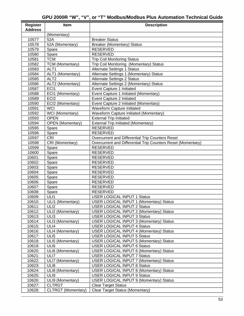
GPU 2000R “W”, “V”, or “T” Modbus/Modbus Plus Automation Technical Guide
53
RegisterAddress
Item Description
(Momentary)10577 52A Breaker Status10578 52A (Momentary) Breaker (Momentary) Status10579 Spare RESERVED10580 Spare RESERVED10581 TCM Trip Coil Monitoring Status10582 TCM (Momentary) Trip Coil Monitoring (Momentary) Status10583 ALT1 Alternate Settings 1 Status10584 ALT1 (Momentary) Alternate Settings 1 (Momentary) Status10585 ALT2 Alternate Settings 2 Status10586 ALT2 (Momentary) Alternate Settings 2 (Momentary) Status10587 ECI1 Event Capture 1 Initiated10588 ECI1 (Momentary) Event Capture 1 Initiated (Momentary)10589 ECI2 Event Capture 2 Initiated10590 ECI2 (Momentary) Event Capture 2 Initiated (Momentary)10591 WCI Waveform Capture Initiated10592 WCI (Momentary) Waveform Capture Initiated (Momentary)10593 OPEN External Trip Initiated10594 OPEN (Momentary) External Trip Initiated (Momentary)10595 Spare RESERVED10596 Spare RESERVED10597 CRI Overcurrent and Differential Trip Counters Reset10598 CRI (Momentary) Overcurrent and Differential Trip Counters Reset (Momentary)10599 Spare RESERVED10600 Spare RESERVED10601: Spare RESERVED10602: Spare RESERVED10603: Spare RESERVED10604: Spare RESERVED10605: Spare RESERVED10606: Spare RESERVED10607: Spare RESERVED10608: Spare RESERVED10609: ULI1 USER LOGICAL INPUT 1 Status10610: ULI1 (Momentary) USER LOGICAL INPUT 1 (Momentary) Status10611: ULI2 USER LOGICAL INPUT 2 Status10612: ULI2 (Momentary) USER LOGICAL INPUT 2 (Momentary) Status10613: ULI3 USER LOGICAL INPUT 3 Status10614: ULI3 (Momentary) USER LOGICAL INPUT 3 (Momentary) Status10615: ULI4 USER LOGICAL INPUT 4 Status10616: ULI4 (Momentary) USER LOGICAL INPUT 4 (Momentary) Status10617: ULI5 USER LOGICAL INPUT 5 Status10618: ULI5 (Momentary) USER LOGICAL INPUT 5 (Momentary) Status10619: ULI6 USER LOGICAL INPUT 6 Status10620: ULI6 (Momentary) USER LOGICAL INPUT 6 (Momentary) Status10621: ULI7 USER LOGICAL INPUT 7 Status10622: ULI7 (Momentary) USER LOGICAL INPUT 7 (Momentary) Status10623: ULI8 USER LOGICAL INPUT 8 Status10624: ULI8 (Momentary) USER LOGICAL INPUT 8 (Momentary) Status10625: ULI9 USER LOGICAL INPUT 9 Status10626: ULI9 (Momentary) USER LOGICAL INPUT 9 (Momentary) Status10627: CLTRGT Clear Target Status10628: CLTRGT (Momentary) Clear Target Status (Momentary)
GPU 2000R “W”, “V”, or “T” Modbus/Modbus Plus Automation Technical Guide
54
RegisterAddress
Item Description
10629: CLSEAL Clear Seal In Element Status10630: CLSEAL (Momentary) Clear Seal In Element Status (Momentary)10631: 64F Field Ground Input from External Relay Status10632: 64F (Momentary) Field Ground Input from External Relay Status (Momentary)10633: Blown Fuse Blown Fuse Indication Status10634: Blown Fuse
(Momentary)Blown Fuse Indication Status (Momentary)
10635: Spare RESERVED10636: Spare RESERVED10637: Spare RESERVED10638: Spare RESERVED10639 Spare RESERVED10640: Spare RESERVED10641: Spare RESERVED10642: Spare RESERVED10643: Spare RESERVED10644: Spare RESERVED10645: Spare RESERVED10646: Spare RESERVED10647: Spare RESERVED10648: Spare RESERVED10649: Spare RESERVED10650: Spare RESERVED10651: IEA Inadvertand Engergization Torque Control Status10652: IEA (Momentary) Inadvertand Engergization Torque Control Status (Momentary)10653: UDI User Defined Message Display Initiated10654: UDI (Momentary) User Defined Message Display Initiated (Momentary)
Application Example: ObtainWinding 1 Phase Time and Winding 2 Phase Time (51P-1 and 51P-2 Status). Therelay status is available from inputs 10517 through 10520 using Momentary Change Detect Bits. Figures 5-21and 5-22 illustrate the polling sequence and raw data returned over the network utilizing function code 02 usingMomentary change detect notification.
Function 02 - Read Input StatusExample - Read Zone 1a and 1 Impedance Torque ControlStatus Bits. Although only 4 data bits are needed, 16 shall beread starting from 10513. Modbus Slave Addr =1
Host Sends : 01 02 02 00 00 10 78 7E Modbus RTU Mode UsedNode Addr = 01Function = 02 Data Address = 512 ( which is 513 [ Modbus is offset by 1] in hex =0200)Amount of Data Requested = 16 InputsCRC-16 Checksum = 78 7ERelay Responds: 01 02 02 61 01 51 E8Addr = 01Function = 02Data Bytes Received = 2Data Received = 61 01CRC - 16 Checksum = 51 E8
Read from 1X Mapping
EC
Figure 5-21. Momentary Change Detect Status Example
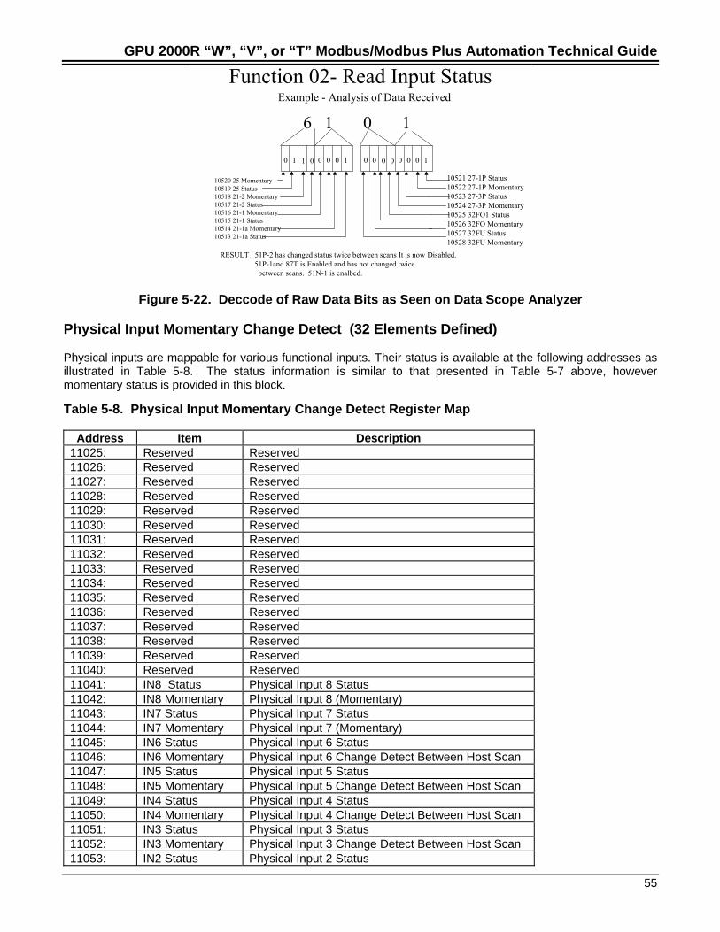
GPU 2000R “W”, “V”, or “T” Modbus/Modbus Plus Automation Technical Guide
55
Function 02- Read Input Status
0 1 1 0 0 0 0 1 0 0 0 0 0 0 0 1
Example - Analysis of Data Received
6 1 0 1
10520 25 Momentary10519 25 Status10518 21-2 Momentary10517 21-2 Status10516 21-1 Momentary10515 21-1 Status10514 21-1a Momentary10513 21-1a Status
10521 27-1P Status10522 27-1P Momentary10523 27-3P Status10524 27-3P Momentary10525 32FO1 Status10526 32FO Momentary10527 32FU Status10528 32FU Momentary
RESULT : 51P-2 has changed status twice between scans It is now Disabled.51P-1and 87T is Enabled and has not changed twicebetween scans. 51N-1 is enalbed.
Figure 5-22. Deccode of Raw Data Bits as Seen on Data Scope Analyzer
Physical Input Momentary Change Detect (32 Elements Defined)
Physical inputs are mappable for various functional inputs. Their status is available at the following addresses asillustrated in Table 5-8. The status information is similar to that presented in Table 5-7 above, howevermomentary status is provided in this block.
Table 5-8. Physical Input Momentary Change Detect Register Map
Address Item Description11025: Reserved Reserved11026: Reserved Reserved11027: Reserved Reserved11028: Reserved Reserved11029: Reserved Reserved11030: Reserved Reserved11031: Reserved Reserved11032: Reserved Reserved11033: Reserved Reserved11034: Reserved Reserved11035: Reserved Reserved11036: Reserved Reserved11037: Reserved Reserved11038: Reserved Reserved11039: Reserved Reserved11040: Reserved Reserved11041: IN8 Status Physical Input 8 Status11042: IN8 Momentary Physical Input 8 (Momentary)11043: IN7 Status Physical Input 7 Status11044: IN7 Momentary Physical Input 7 (Momentary)11045: IN6 Status Physical Input 6 Status11046: IN6 Momentary Physical Input 6 Change Detect Between Host Scan11047: IN5 Status Physical Input 5 Status11048: IN5 Momentary Physical Input 5 Change Detect Between Host Scan11049: IN4 Status Physical Input 4 Status11050: IN4 Momentary Physical Input 4 Change Detect Between Host Scan11051: IN3 Status Physical Input 3 Status11052: IN3 Momentary Physical Input 3 Change Detect Between Host Scan11053: IN2 Status Physical Input 2 Status
GPU 2000R “W”, “V”, or “T” Modbus/Modbus Plus Automation Technical Guide
56
Address Item Description11054: IN2 Momentary Physical Input 2 Change Detect Between Host Scan11055: IN1 Status Physical Input 1 Status11056: IN1 Momentary Physical Input 1 Change Detect Between Host Scan
4X Register Read Capabilities
The GPU 2000R implementation of 4X registers allow for both status reads and in limited cases for controlregister writes. Many host devices do not allow the access of data from discrete data types (such as 0X and 1Xdiscrete output and input function codes). The Modbus implementation within the GPU 2000R “V”, W” and “T”relays allow for Modbus commands 03, 16 (10 hex), 06, and 23 (17 hex) register commands. Real time relaystatus is available for the following relay data types and functionality:
• Relay Status• Diagnostic Status• Unit Information• CT and PT Information• Physical Input Status• Logical Input Status• Physical Output Status• Logical Output Status• Load Metering Data• Demand Metering Data• Master Trip Functionality• Fault Record Buffering (1- 32)• Event Record Buffering (1- 128)• Breaker Counter Operation Retrieval• Force of Physical Outputs• Breaker Control Functions over the network• Reset of Counter, Event Buffer, Operational Buffer, Seal In and Target information
Each function code and data type shall be explained in detail, within the following sections.
Modbus protocol allows a variety of information to be placed within the 4X register types. The interpretation of thereturned data is key to data received in the request. Modbus protocol is predicated upon register informationbeing returned. A register is 2 bytes, or 16 bits which translates into one word. Multiple words may be combinedto form a longer word which allows a larger read to obtained from the GPU 2000R. The GPU 2000R supportsthe following data return types for 4X formats:
• Unsigned - 16 bits - 2 bytes - Range 0 to + 65,535• Signed - 16 bits - 2 bytes - Range –32,768 to 32,767• Unsigned Long - 32 bits - 4 bytes - Range 0 to +4,294,967,295• Signed Long - 32 bits - 4 bytes - Range -2,147,483,648 to +2,147,483,647• ASCII - 16 bits - 2 bytes - 2 characters per register (Reference Appendix B)
The tables contained within this document reference the above definitions and give the cadence of bytes or wordsas:
• MSB Most Significant Byte• LSB Least Significant Byte• MSW Most Significant Word• LSW Least Significant Word• Msb Most signficant bit• Lsb Least significant bit
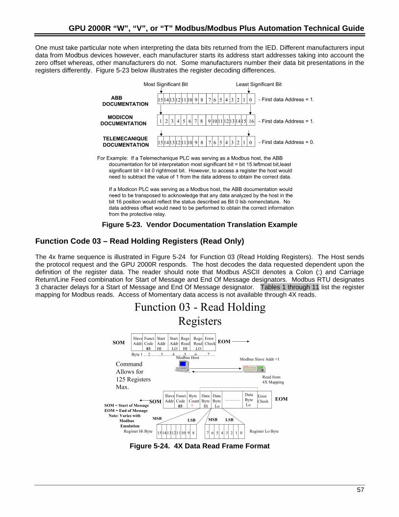
GPU 2000R “W”, “V”, or “T” Modbus/Modbus Plus Automation Technical Guide
57
One must take particular note when interpreting the data bits returned from the IED. Different manufacturers inputdata from Modbus devices however, each manufacturer starts its address start addresses taking into account thezero offset whereas, other manufacturers do not. Some manufacturers number their data bit presentations in theregisters differently. Figure 5-23 below illustrates the register decoding differences.
ABB DOCUMENTATION
Most Significant Bit Least Significant Bit
1514131211 10 9 8 7 6 5 4 3 2 1 0 - First data Address = 1.
MODICON DOCUMENTATION 1 2 3 4 5 6 7 8 9 101112131415 16 - First data Address = 1.
TELEMECANIQUEDOCUMENTATION 1514131211 10 9 8 7 6 5 4 3 2 1 0 - First data Address = 0.
For Example: If a Telemechanique PLC was serving as a Modbus host, the ABB documentation for bit interpretation most significant bit = bit 15 leftmost bit,least significant bit = bit 0 rightmost bit. However, to access a register the host would need to subtract the value of 1 from the data address to obtain the correct data.
If a Modicon PLC was serving as a Modbus host, the ABB documentation would need to be transposed to acknowledge that any data analyzed by the host in the bit 16 position would reflect the status described as Bit 0 lsb nomenclature. No data address offset would need to be performed to obtain the correct information from the protective relay.
Figure 5-23. Vendor Documentation Translation Example
Function Code 03 – Read Holding Registers (Read Only)
The 4x frame sequence is illustrated in Figure 5-24 for Function 03 (Read Holding Registers). The Host sendsthe protocol request and the GPU 2000R responds. The host decodes the data requested dependent upon thedefinition of the register data. The reader should note that Modbus ASCII denotes a Colon (:) and CarriageReturn/Line Feed combination for Start of Message and End Of Message designators. Modbus RTU designates3 character delays for a Start of Message and End Of Message designator. Tables 1 through 11 list the registermapping for Modbus reads. Access of Momentary data access is not available through 4X reads.
Function 03 - Read HoldingRegisters
Modbus Host Modbus Slave Addr =1
Read from 4X Mapping
SlaveAddr.
Funct.Code 03
StartAddrHI
Start Addr LO
RegsRead HI
RegsRead LO
ErrorCheck EOMSOM
Byte 1 …2……..3…….4…….5……6……..7….
Register Lo Byte
CommandAllows for125 RegistersMax.
SlaveAddr.
Funct.Code 03
ByteCount *
DataByte Hi
DataByte Lo
DataByte Lo
ErrorCheck EOMSOM
MSB LSB
15 141312 1110 9 8 7 6 5 4 3 2 1 0
MSB LSB
Register Hi Byte
SOM = Start of MessageEOM = End of Message Note: Varies with Modbus Emulation
EC
Figure 5-24. 4X Data Read Frame Format
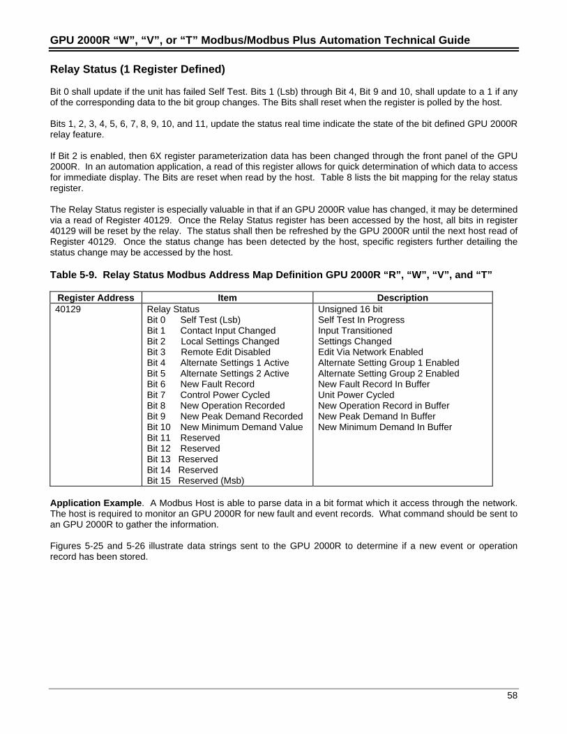
GPU 2000R “W”, “V”, or “T” Modbus/Modbus Plus Automation Technical Guide
58
Relay Status (1 Register Defined)
Bit 0 shall update if the unit has failed Self Test. Bits 1 (Lsb) through Bit 4, Bit 9 and 10, shall update to a 1 if anyof the corresponding data to the bit group changes. The Bits shall reset when the register is polled by the host.
Bits 1, 2, 3, 4, 5, 6, 7, 8, 9, 10, and 11, update the status real time indicate the state of the bit defined GPU 2000Rrelay feature.
If Bit 2 is enabled, then 6X register parameterization data has been changed through the front panel of the GPU2000R. In an automation application, a read of this register allows for quick determination of which data to accessfor immediate display. The Bits are reset when read by the host. Table 8 lists the bit mapping for the relay statusregister.
The Relay Status register is especially valuable in that if an GPU 2000R value has changed, it may be determinedvia a read of Register 40129. Once the Relay Status register has been accessed by the host, all bits in register40129 will be reset by the relay. The status shall then be refreshed by the GPU 2000R until the next host read ofRegister 40129. Once the status change has been detected by the host, specific registers further detailing thestatus change may be accessed by the host.
Table 5-9. Relay Status Modbus Address Map Definition GPU 2000R “R”, “W”, “V”, and “T”
Register Address Item Description40129 Relay Status
Bit 0 Self Test (Lsb)Bit 1 Contact Input ChangedBit 2 Local Settings ChangedBit 3 Remote Edit DisabledBit 4 Alternate Settings 1 ActiveBit 5 Alternate Settings 2 ActiveBit 6 New Fault RecordBit 7 Control Power CycledBit 8 New Operation RecordedBit 9 New Peak Demand RecordedBit 10 New Minimum Demand ValueBit 11 ReservedBit 12 ReservedBit 13 ReservedBit 14 ReservedBit 15 Reserved (Msb)
Unsigned 16 bitSelf Test In ProgressInput TransitionedSettings ChangedEdit Via Network EnabledAlternate Setting Group 1 EnabledAlternate Setting Group 2 EnabledNew Fault Record In BufferUnit Power CycledNew Operation Record in BufferNew Peak Demand In BufferNew Minimum Demand In Buffer
Application Example. A Modbus Host is able to parse data in a bit format which it access through the network.The host is required to monitor an GPU 2000R for new fault and event records. What command should be sent toan GPU 2000R to gather the information.
Figures 5-25 and 5-26 illustrate data strings sent to the GPU 2000R to determine if a new event or operationrecord has been stored.
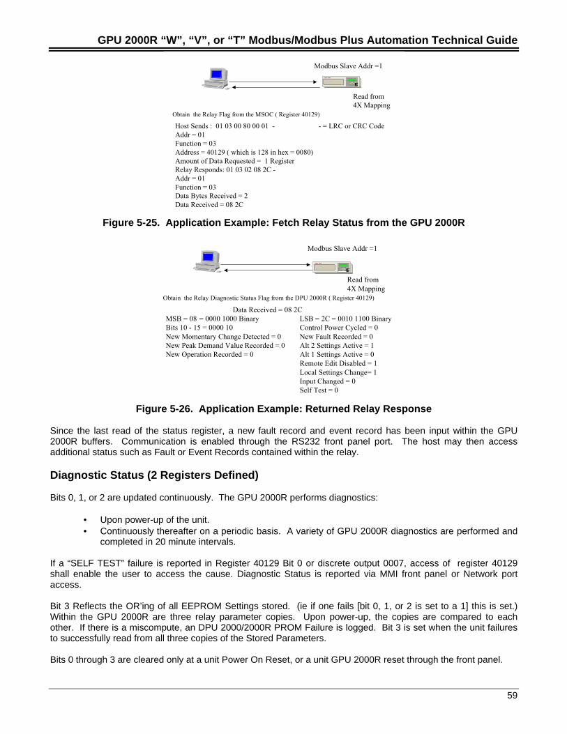
GPU 2000R “W”, “V”, or “T” Modbus/Modbus Plus Automation Technical Guide
59
Modbus Slave Addr =1
Read from 4X Mapping
Obtain the Relay Flag from the MSOC ( Register 40129)
Host Sends : 01 03 00 80 00 01 - - = LRC or CRC CodeAddr = 01Function = 03Address = 40129 ( which is 128 in hex = 0080)Amount of Data Requested = 1 RegisterRelay Responds: 01 03 02 08 2C -Addr = 01Function = 03Data Bytes Received = 2Data Received = 08 2C
EC
Figure 5-25. Application Example: Fetch Relay Status from the GPU 2000R
Modbus Slave Addr =1
Read from 4X Mapping
Obtain the Relay Diagnostic Status Flag from the DPU 2000R ( Register 40129)
Data Received = 08 2CMSB = 08 = 0000 1000 Binary LSB = 2C = 0010 1100 BinaryBits 10 - 15 = 0000 10 Control Power Cycled = 0New Momentary Change Detected = 0 New Fault Recorded = 0New Peak Demand Value Recorded = 0 Alt 2 Settings Active = 1New Operation Recorded = 0 Alt 1 Settings Active = 0
Remote Edit Disabled = 1Local Settings Change= 1Input Changed = 0Self Test = 0
EC
Figure 5-26. Application Example: Returned Relay Response
Since the last read of the status register, a new fault record and event record has been input within the GPU2000R buffers. Communication is enabled through the RS232 front panel port. The host may then accessadditional status such as Fault or Event Records contained within the relay.
Diagnostic Status (2 Registers Defined)
Bits 0, 1, or 2 are updated continuously. The GPU 2000R performs diagnostics:
• Upon power-up of the unit.• Continuously thereafter on a periodic basis. A variety of GPU 2000R diagnostics are performed and
completed in 20 minute intervals.
If a “SELF TEST” failure is reported in Register 40129 Bit 0 or discrete output 0007, access of register 40129shall enable the user to access the cause. Diagnostic Status is reported via MMI front panel or Network portaccess.
Bit 3 Reflects the OR’ing of all EEPROM Settings stored. (ie if one fails [bit 0, 1, or 2 is set to a 1] this is set.)Within the GPU 2000R are three relay parameter copies. Upon power-up, the copies are compared to eachother. If there is a miscompute, an DPU 2000/2000R PROM Failure is logged. Bit 3 is set when the unit failuresto successfully read from all three copies of the Stored Parameters.
Bits 0 through 3 are cleared only at a unit Power On Reset, or a unit GPU 2000R reset through the front panel.
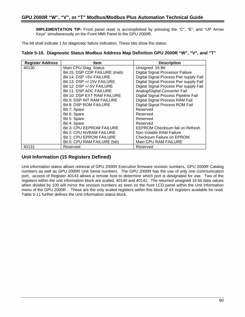
GPU 2000R “W”, “V”, or “T” Modbus/Modbus Plus Automation Technical Guide
60
IMPLEMENTATION TIP- Front panel reset is accomplished by pressing the “C”, “E”, and “UP ArrowKeys” simultaneously on the Front MMI Panel fo the GPU 2000R.
The bit shall indicate 1 for diagnostic failure indication. These bits show the status.
Table 5-10. Diagnostic Status Modbus Address Map Definition GPU 2000R “W”, “V”, and “T”
Register Address Item Description40130 Main CPU Diag. Status
Bit 15: DSP COP FAILURE (msb)Bit 14: DSP +5V FAILUREBit 13: DSP +/-15V FAILUREBit 12: DSP +/-5V FAILUREBit 11: DSP ADC FAILUREBit 10: DSP EXT RAM FAILUREBit 9: DSP INT RAM FAILUREBit 8: DSP ROM FAILUREBit 7: SpareBit 6: SpareBit 5: SpareBit 4: SpareBit 3: CPU EEPROM FAILUREBit 2: CPU NVRAM FAILUREBit 1: CPU EPROM FAILUREBit 0: CPU RAM FAILURE (lsb)
Unsigned 16 BitDigital Signal Processor FailureDigital Signal Process Pwr supply FailDigital Signal Process Pwr supply FailDigital Signal Process Pwr supply FailAnalog/Digital Converter FailDigital Signal Process Pipeline FailDigital Signal Process RAM FailDigital Signal Process ROM FailReservedReservedReservedReservedEEPROM Checksum fail on RefreshNon-Volatile RAM FailureChecksum Failure on EPROMMain CPU RAM FAILURE
40131 Reserved Reserved
Unit Information (15 Registers Defined)
Unit information status allows retrieval of GPU 2000R Executive firmware revision numbers, GPU 2000R Catalognumbers as well as GPU 2000R Unit Serial numbers. The GPU 2000R has the use of only one communicationport, access of Register 40143 allows a remote host to determine which port is designated for use. Two of theregisters within the unit information block are scaled, 40140 and 40141. The returned unsigned 16 bit data valueswhen divided by 100 will mirror the revision numbers as seen on the front LCD panel within the Unit Informationmenu of the GPU 2000R . These are the only scaled registers within this block of 4X registers available for read.Table 5-11 further defines the Unit Information status block.
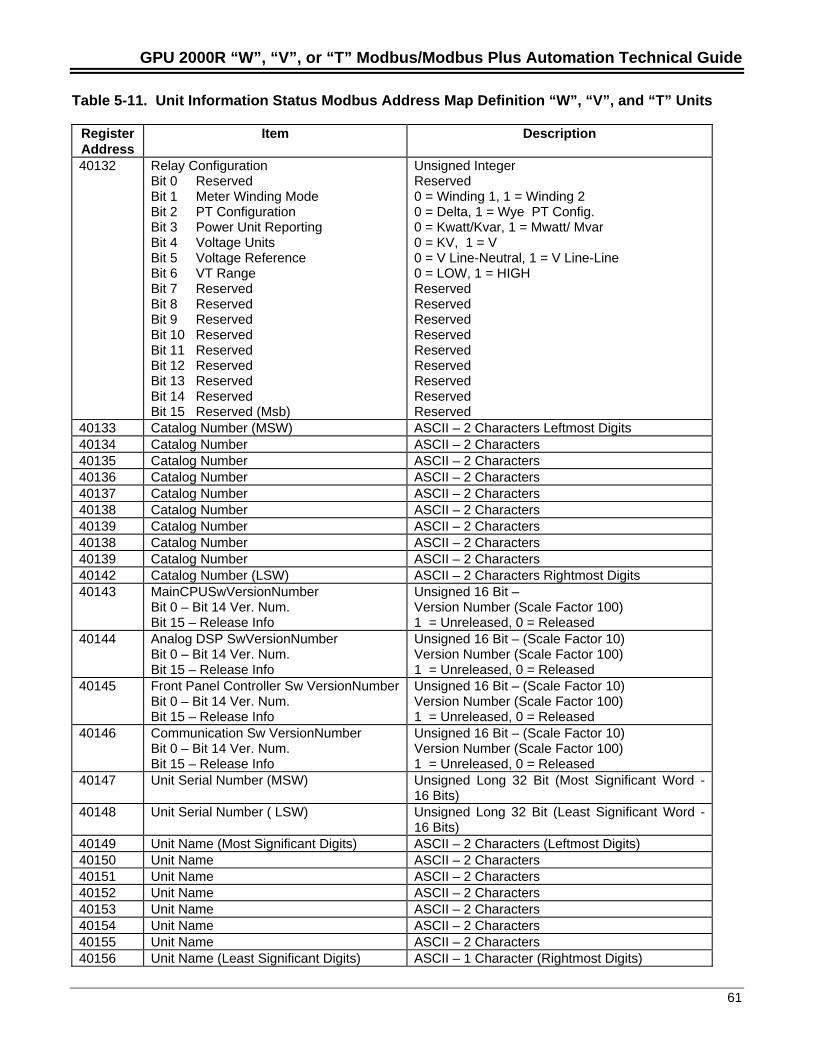
GPU 2000R “W”, “V”, or “T” Modbus/Modbus Plus Automation Technical Guide
61
Table 5-11. Unit Information Status Modbus Address Map Definition “W”, “V”, and “T” Units
RegisterAddress
Item Description
40132 Relay ConfigurationBit 0 ReservedBit 1 Meter Winding ModeBit 2 PT ConfigurationBit 3 Power Unit ReportingBit 4 Voltage UnitsBit 5 Voltage ReferenceBit 6 VT RangeBit 7 ReservedBit 8 ReservedBit 9 ReservedBit 10 ReservedBit 11 ReservedBit 12 ReservedBit 13 ReservedBit 14 ReservedBit 15 Reserved (Msb)
Unsigned IntegerReserved0 = Winding 1, 1 = Winding 20 = Delta, 1 = Wye PT Config.0 = Kwatt/Kvar, 1 = Mwatt/ Mvar0 = KV, 1 = V0 = V Line-Neutral, 1 = V Line-Line0 = LOW, 1 = HIGHReservedReservedReservedReservedReservedReservedReservedReservedReserved
40133 Catalog Number (MSW) ASCII – 2 Characters Leftmost Digits40134 Catalog Number ASCII – 2 Characters40135 Catalog Number ASCII – 2 Characters40136 Catalog Number ASCII – 2 Characters40137 Catalog Number ASCII – 2 Characters40138 Catalog Number ASCII – 2 Characters40139 Catalog Number ASCII – 2 Characters40138 Catalog Number ASCII – 2 Characters40139 Catalog Number ASCII – 2 Characters40142 Catalog Number (LSW) ASCII – 2 Characters Rightmost Digits40143 MainCPUSwVersionNumber
Bit 0 – Bit 14 Ver. Num.Bit 15 – Release Info
Unsigned 16 Bit –Version Number (Scale Factor 100)1 = Unreleased, 0 = Released
40144 Analog DSP SwVersionNumberBit 0 – Bit 14 Ver. Num.Bit 15 – Release Info
Unsigned 16 Bit – (Scale Factor 10)Version Number (Scale Factor 100)1 = Unreleased, 0 = Released
40145 Front Panel Controller Sw VersionNumberBit 0 – Bit 14 Ver. Num.Bit 15 – Release Info
Unsigned 16 Bit – (Scale Factor 10)Version Number (Scale Factor 100)1 = Unreleased, 0 = Released
40146 Communication Sw VersionNumberBit 0 – Bit 14 Ver. Num.Bit 15 – Release Info
Unsigned 16 Bit – (Scale Factor 10)Version Number (Scale Factor 100)1 = Unreleased, 0 = Released
40147 Unit Serial Number (MSW) Unsigned Long 32 Bit (Most Significant Word -16 Bits)
40148 Unit Serial Number ( LSW) Unsigned Long 32 Bit (Least Significant Word -16 Bits)
40149 Unit Name (Most Significant Digits) ASCII – 2 Characters (Leftmost Digits)40150 Unit Name ASCII – 2 Characters40151 Unit Name ASCII – 2 Characters40152 Unit Name ASCII – 2 Characters40153 Unit Name ASCII – 2 Characters40154 Unit Name ASCII – 2 Characters40155 Unit Name ASCII – 2 Characters40156 Unit Name (Least Significant Digits) ASCII – 1 Character (Rightmost Digits)
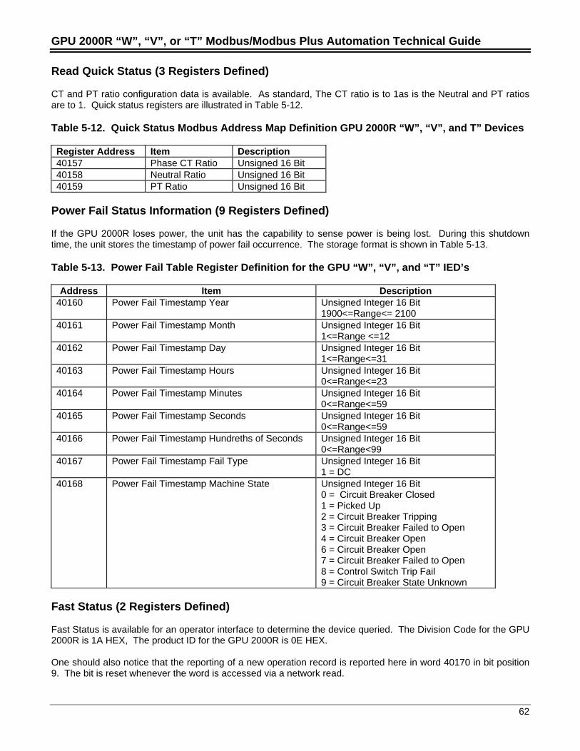
GPU 2000R “W”, “V”, or “T” Modbus/Modbus Plus Automation Technical Guide
62
Read Quick Status (3 Registers Defined)
CT and PT ratio configuration data is available. As standard, The CT ratio is to 1as is the Neutral and PT ratiosare to 1. Quick status registers are illustrated in Table 5-12.
Table 5-12. Quick Status Modbus Address Map Definition GPU 2000R “W”, “V”, and T” Devices
Register Address Item Description40157 Phase CT Ratio Unsigned 16 Bit40158 Neutral Ratio Unsigned 16 Bit40159 PT Ratio Unsigned 16 Bit
Power Fail Status Information (9 Registers Defined)
If the GPU 2000R loses power, the unit has the capability to sense power is being lost. During this shutdowntime, the unit stores the timestamp of power fail occurrence. The storage format is shown in Table 5-13.
Table 5-13. Power Fail Table Register Definition for the GPU “W”, “V”, and “T” IED’s
Address Item Description40160 Power Fail Timestamp Year Unsigned Integer 16 Bit
1900<=Range<= 210040161 Power Fail Timestamp Month Unsigned Integer 16 Bit
1<=Range <=1240162 Power Fail Timestamp Day Unsigned Integer 16 Bit
1<=Range<=3140163 Power Fail Timestamp Hours Unsigned Integer 16 Bit
0<=Range<=2340164 Power Fail Timestamp Minutes Unsigned Integer 16 Bit
0<=Range<=5940165 Power Fail Timestamp Seconds Unsigned Integer 16 Bit
0<=Range<=5940166 Power Fail Timestamp Hundreths of Seconds Unsigned Integer 16 Bit
0<=Range<9940167 Power Fail Timestamp Fail Type Unsigned Integer 16 Bit
1 = DC40168 Power Fail Timestamp Machine State Unsigned Integer 16 Bit
0 = Circuit Breaker Closed1 = Picked Up2 = Circuit Breaker Tripping3 = Circuit Breaker Failed to Open4 = Circuit Breaker Open6 = Circuit Breaker Open7 = Circuit Breaker Failed to Open8 = Control Switch Trip Fail9 = Circuit Breaker State Unknown
Fast Status (2 Registers Defined)
Fast Status is available for an operator interface to determine the device queried. The Division Code for the GPU2000R is 1A HEX, The product ID for the GPU 2000R is 0E HEX.
One should also notice that the reporting of a new operation record is reported here in word 40170 in bit position9. The bit is reset whenever the word is accessed via a network read.
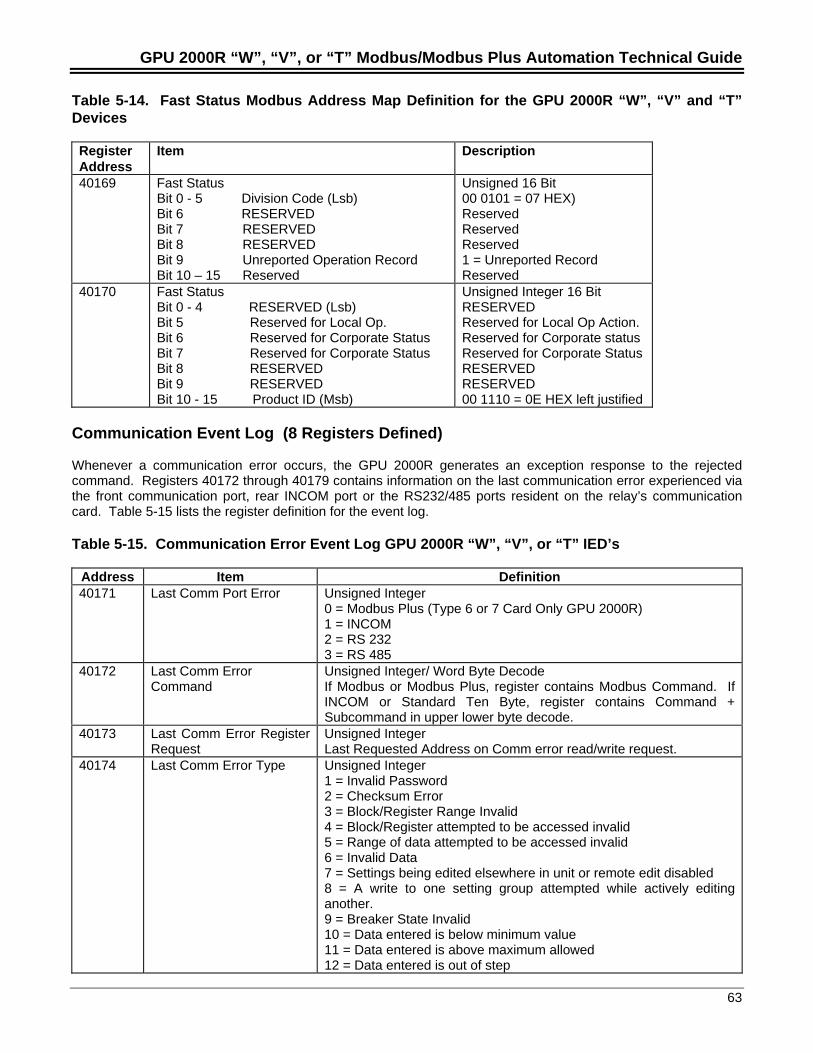
GPU 2000R “W”, “V”, or “T” Modbus/Modbus Plus Automation Technical Guide
63
Table 5-14. Fast Status Modbus Address Map Definition for the GPU 2000R “W”, “V” and “T”Devices
RegisterAddress
Item Description
40169 Fast StatusBit 0 - 5 Division Code (Lsb)Bit 6 RESERVEDBit 7 RESERVEDBit 8 RESERVEDBit 9 Unreported Operation RecordBit 10 – 15 Reserved
Unsigned 16 Bit00 0101 = 07 HEX)ReservedReservedReserved1 = Unreported RecordReserved
40170 Fast StatusBit 0 - 4 RESERVED (Lsb)Bit 5 Reserved for Local Op.Bit 6 Reserved for Corporate StatusBit 7 Reserved for Corporate StatusBit 8 RESERVEDBit 9 RESERVEDBit 10 - 15 Product ID (Msb)
Unsigned Integer 16 BitRESERVEDReserved for Local Op Action.Reserved for Corporate statusReserved for Corporate StatusRESERVEDRESERVED00 1110 = 0E HEX left justified
Communication Event Log (8 Registers Defined)
Whenever a communication error occurs, the GPU 2000R generates an exception response to the rejectedcommand. Registers 40172 through 40179 contains information on the last communication error experienced viathe front communication port, rear INCOM port or the RS232/485 ports resident on the relay’s communicationcard. Table 5-15 lists the register definition for the event log.
Table 5-15. Communication Error Event Log GPU 2000R “W”, “V”, or “T” IED’s
Address Item Definition40171 Last Comm Port Error Unsigned Integer
0 = Modbus Plus (Type 6 or 7 Card Only GPU 2000R)1 = INCOM2 = RS 2323 = RS 485
40172 Last Comm ErrorCommand
Unsigned Integer/ Word Byte DecodeIf Modbus or Modbus Plus, register contains Modbus Command. IfINCOM or Standard Ten Byte, register contains Command +Subcommand in upper lower byte decode.
40173 Last Comm Error RegisterRequest
Unsigned IntegerLast Requested Address on Comm error read/write request.
40174 Last Comm Error Type Unsigned Integer1 = Invalid Password2 = Checksum Error3 = Block/Register Range Invalid4 = Block/Register attempted to be accessed invalid5 = Range of data attempted to be accessed invalid6 = Invalid Data7 = Settings being edited elsewhere in unit or remote edit disabled8 = A write to one setting group attempted while actively editinganother.9 = Breaker State Invalid10 = Data entered is below minimum value11 = Data entered is above maximum allowed12 = Data entered is out of step
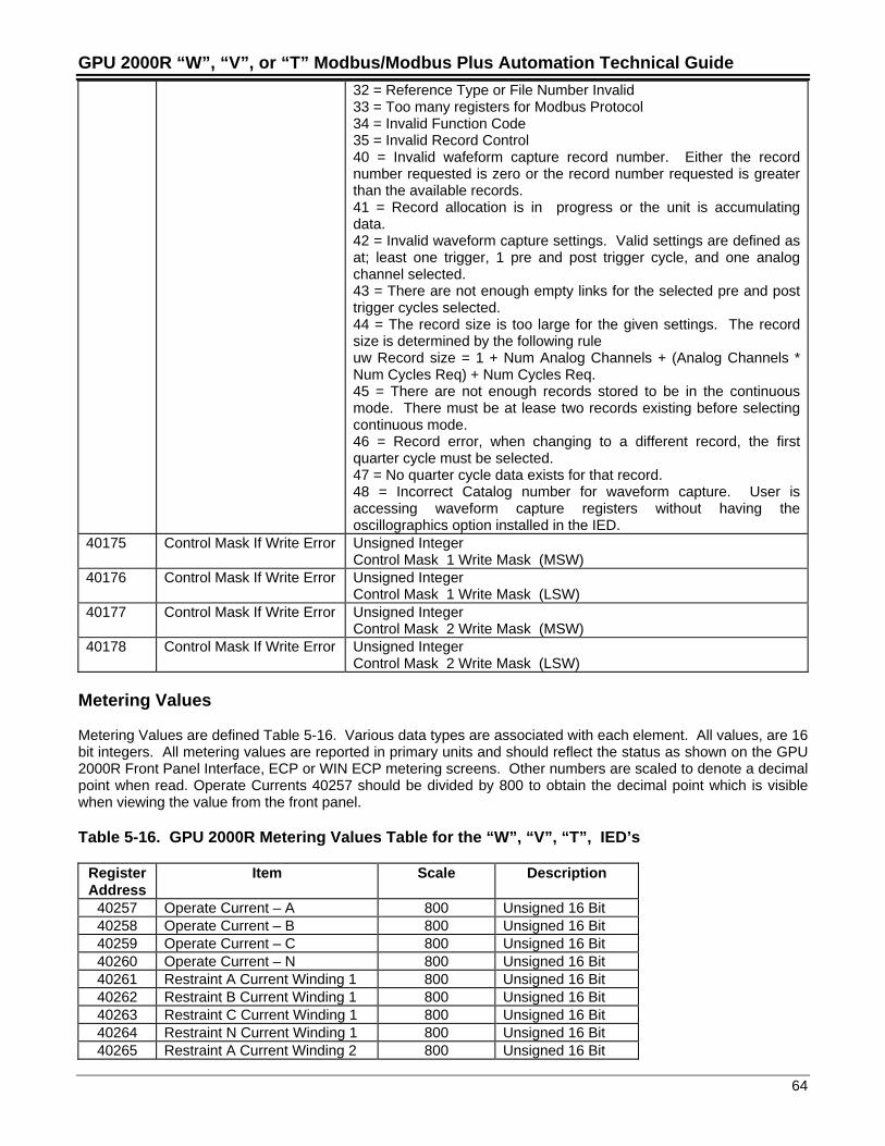
GPU 2000R “W”, “V”, or “T” Modbus/Modbus Plus Automation Technical Guide
64
32 = Reference Type or File Number Invalid33 = Too many registers for Modbus Protocol34 = Invalid Function Code35 = Invalid Record Control40 = Invalid wafeform capture record number. Either the recordnumber requested is zero or the record number requested is greaterthan the available records.41 = Record allocation is in progress or the unit is accumulatingdata.42 = Invalid waveform capture settings. Valid settings are defined asat; least one trigger, 1 pre and post trigger cycle, and one analogchannel selected.43 = There are not enough empty links for the selected pre and posttrigger cycles selected.44 = The record size is too large for the given settings. The recordsize is determined by the following ruleuw Record size = 1 + Num Analog Channels + (Analog Channels *Num Cycles Req) + Num Cycles Req.45 = There are not enough records stored to be in the continuousmode. There must be at lease two records existing before selectingcontinuous mode.46 = Record error, when changing to a different record, the firstquarter cycle must be selected.47 = No quarter cycle data exists for that record.48 = Incorrect Catalog number for waveform capture. User isaccessing waveform capture registers without having theoscillographics option installed in the IED.
40175 Control Mask If Write Error Unsigned IntegerControl Mask 1 Write Mask (MSW)
40176 Control Mask If Write Error Unsigned IntegerControl Mask 1 Write Mask (LSW)
40177 Control Mask If Write Error Unsigned IntegerControl Mask 2 Write Mask (MSW)
40178 Control Mask If Write Error Unsigned IntegerControl Mask 2 Write Mask (LSW)
Metering Values
Metering Values are defined Table 5-16. Various data types are associated with each element. All values, are 16bit integers. All metering values are reported in primary units and should reflect the status as shown on the GPU2000R Front Panel Interface, ECP or WIN ECP metering screens. Other numbers are scaled to denote a decimalpoint when read. Operate Currents 40257 should be divided by 800 to obtain the decimal point which is visiblewhen viewing the value from the front panel.
Table 5-16. GPU 2000R Metering Values Table for the “W”, “V”, “T”, IED’s
RegisterAddress
Item Scale Description
40257 Operate Current – A 800 Unsigned 16 Bit40258 Operate Current – B 800 Unsigned 16 Bit40259 Operate Current – C 800 Unsigned 16 Bit40260 Operate Current – N 800 Unsigned 16 Bit40261 Restraint A Current Winding 1 800 Unsigned 16 Bit40262 Restraint B Current Winding 1 800 Unsigned 16 Bit40263 Restraint C Current Winding 1 800 Unsigned 16 Bit40264 Restraint N Current Winding 1 800 Unsigned 16 Bit40265 Restraint A Current Winding 2 800 Unsigned 16 Bit
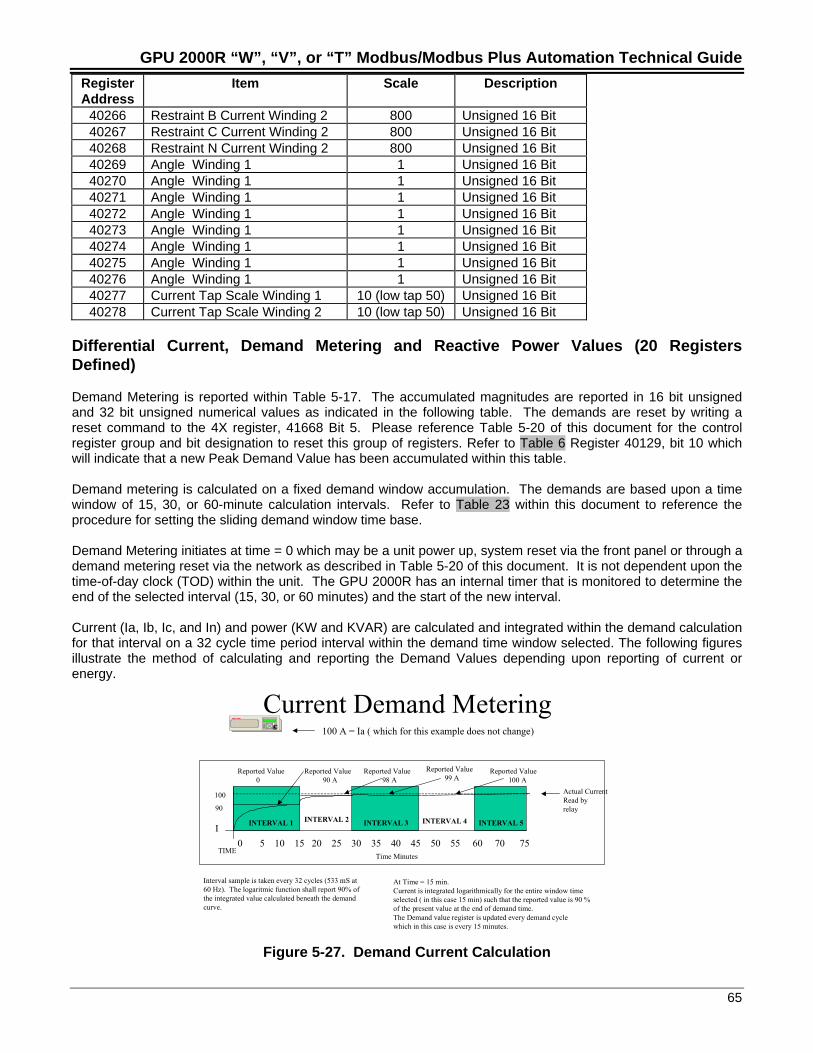
GPU 2000R “W”, “V”, or “T” Modbus/Modbus Plus Automation Technical Guide
65
RegisterAddress
Item Scale Description
40266 Restraint B Current Winding 2 800 Unsigned 16 Bit40267 Restraint C Current Winding 2 800 Unsigned 16 Bit40268 Restraint N Current Winding 2 800 Unsigned 16 Bit40269 Angle Winding 1 1 Unsigned 16 Bit40270 Angle Winding 1 1 Unsigned 16 Bit40271 Angle Winding 1 1 Unsigned 16 Bit40272 Angle Winding 1 1 Unsigned 16 Bit40273 Angle Winding 1 1 Unsigned 16 Bit40274 Angle Winding 1 1 Unsigned 16 Bit40275 Angle Winding 1 1 Unsigned 16 Bit40276 Angle Winding 1 1 Unsigned 16 Bit40277 Current Tap Scale Winding 1 10 (low tap 50) Unsigned 16 Bit40278 Current Tap Scale Winding 2 10 (low tap 50) Unsigned 16 Bit
Differential Current, Demand Metering and Reactive Power Values (20 RegistersDefined)
Demand Metering is reported within Table 5-17. The accumulated magnitudes are reported in 16 bit unsignedand 32 bit unsigned numerical values as indicated in the following table. The demands are reset by writing areset command to the 4X register, 41668 Bit 5. Please reference Table 5-20 of this document for the controlregister group and bit designation to reset this group of registers. Refer to Table 6 Register 40129, bit 10 whichwill indicate that a new Peak Demand Value has been accumulated within this table.
Demand metering is calculated on a fixed demand window accumulation. The demands are based upon a timewindow of 15, 30, or 60-minute calculation intervals. Refer to Table 23 within this document to reference theprocedure for setting the sliding demand window time base.
Demand Metering initiates at time = 0 which may be a unit power up, system reset via the front panel or through ademand metering reset via the network as described in Table 5-20 of this document. It is not dependent upon thetime-of-day clock (TOD) within the unit. The GPU 2000R has an internal timer that is monitored to determine theend of the selected interval (15, 30, or 60 minutes) and the start of the new interval.
Current (Ia, Ib, Ic, and In) and power (KW and KVAR) are calculated and integrated within the demand calculationfor that interval on a 32 cycle time period interval within the demand time window selected. The following figuresillustrate the method of calculating and reporting the Demand Values depending upon reporting of current orenergy.
Current Demand Metering100 A = Ia ( which for this example does not change)
Time Minutes
I0 5 10 15 20 25 30 35 40 45 50 55 60 70 75
90
At Time = 15 min.Current is integrated logarithmically for the entire window timeselected ( in this case 15 min) such that the reported value is 90 %of the present value at the end of demand time.The Demand value register is updated every demand cyclewhich in this case is every 15 minutes.
100
INTERVAL 1
TIME
Actual CurrentRead by relay
INTERVAL 2 INTERVAL 3
Interval sample is taken every 32 cycles (533 mS at60 Hz). The logaritmic function shall report 90% of the integrated value calculated beneath the demand curve.
Reported Value 0
Reported Value 90 A
Reported Value 98 A
INTERVAL 4 INTERVAL 5
Reported Value 99 A
Reported Value 100 A
EC
Figure 5-27. Demand Current Calculation

GPU 2000R “W”, “V”, or “T” Modbus/Modbus Plus Automation Technical Guide
66
Energy Demand Metering1000 KW ( which for this example does not change)
Time Minutes
KW0 5 10 15 20 25 30 35 40 45 50 55 60 70 75
At Time window end= 15 min,(selected demand interval), 30 minutes,45 minutes,...the relay updates the demand register with the calculatedenergy value.
If the relay is reset prior to the demand window time elapsing,the time shall reset to 0.
1000
TIME
ActualEnergyCalculated by relay.INTERVAL 1
Interval sample is taken every 1/15 th of the selected demand interval (in this case every minute).The logarithmic function shall report 90% of theintegrated value calculated beneath the demand curve.
Reported Value 0
Reported Value 900 KW
Reported Value 900 KW
Reported Value 900 KW
Reported Value 900 KW
900
INTERVAL 2 INTERVAL 3 INTERVAL 4
EC
Figure 5-28. Energy Demand Calculation
Figures 5-27 and 5-28 illustrate the energy and current calculation methods and data reported when accessedvia the network. To simplify the explanation, the current and energy has been kept constant. This exampleillustrates a calculation based upon a window size of 15 minute demand intervals.
Table 5-17. RMS Load Current/Angular Values Block Metering Modbus Address Map Definitionfor the GPU 2000R “R”, “W”, “V”, and “T” Models
RegisterAddress
Item Description
40385 Load Current A Winding 1 Unsigned 32 Bit High Order Word MSW40386 Load Current A Winding 1 Unsigned 32 Bit Low Order Word LSW40387 Load Current B Winding 1 Unsigned 32 Bit High Order Word MSW40388 Load Current B Winding 1 Unsigned 32 Bit Low Order Word LSW40389 Load Current C Winding 1 Unsigned 32 Bit High Order Word MSW40390 Load Current C Winding 1 Unsigned 32 Bit Low Order Word LSW40391 Load Current N Winding 1 Unsigned 32 Bit High Order Word MSW40392 Load Current N Winding 1 Unsigned 32 Bit Low Order Word LSW40393 Load Current A Winding 2 Unsigned 32 Bit High Order Word MSW40394 Load Current A Winding 2 Unsigned 32 Bit Low Order Word LSW40395 Load Current B Winding 2 Unsigned 32 Bit High Order Word MSW40396 Load Current B Winding 2 Unsigned 32 Bit Low Order Word LSW40397 Load Current C Winding 2 Unsigned 32 Bit High Order Word MSW40398 Load Current C Winding 2 Unsigned 32 Bit Low Order Word LSW40399 Load Current N Winding 2 Unsigned 32 Bit High Order Word MSW40400 Load Current N Winding 2 Unsigned 32 Bit Low Order Word LSW40401 Load Current A Angle Winding 1 Unsigned 16 Bit Integer40402 Load Current B Angle Winding 1 Unsigned 16 Bit Integer40403 Load Current C Angle Winding 1 Unsigned 16 Bit Integer40404 Load Current N Angle Winding 1 Unsigned 16 Bit Integer40405 Neutral Current A Angle Winding 2 Unsigned 16 Bit Integer40406 Neutral Current B Angle Winding 2 Unsigned 16 Bit Integer40407 Neutral Current C Angle Winding 2 Unsigned 16 Bit Integer40408 Neutral Current N Angle Winding 2 Unsigned 16 Bit Integer40409 Load Current Zero Sequence Winding 1 Unsigned 32 Bit High Order Word MSW40410 Load Current Zero Sequence Winding 1 Unsigned 32 Bit Low Order Word LSW40411 Load Current Positive Sequence Winding 1 Unsigned 32 Bit High Order Word MSW40412 Load Current Positive Sequence Winding 1 Unsigned 32 Bit Low Order Word LSW
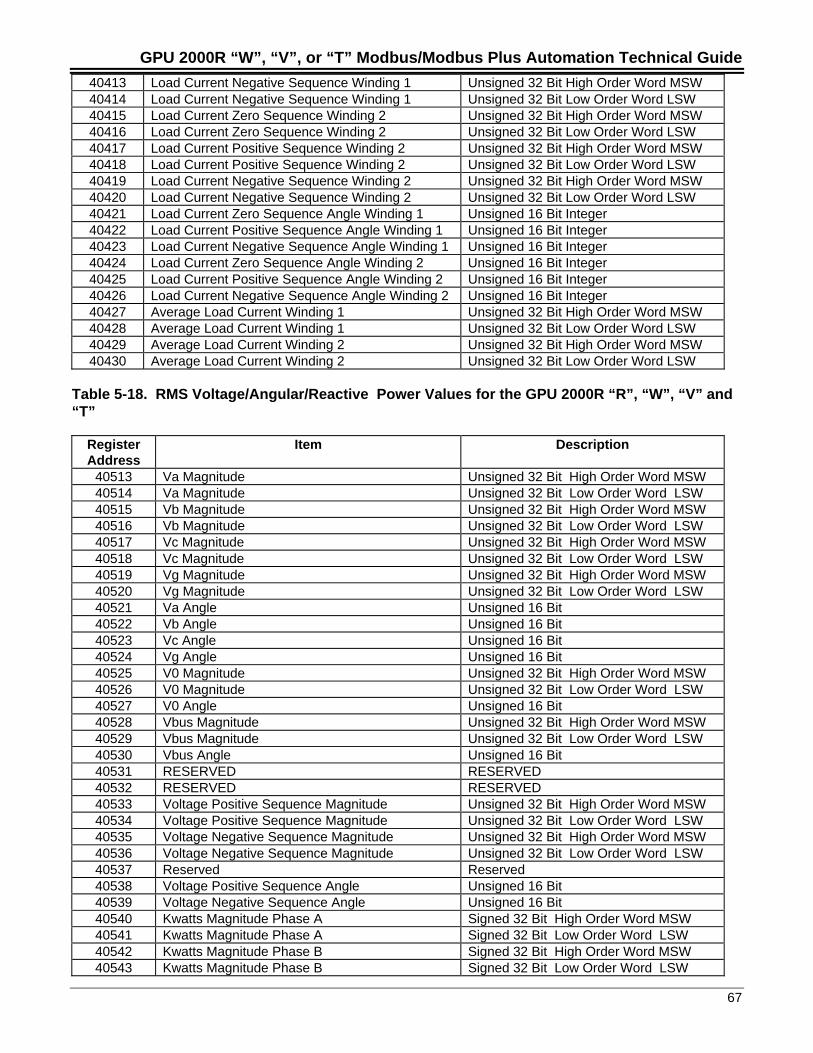
GPU 2000R “W”, “V”, or “T” Modbus/Modbus Plus Automation Technical Guide
67
40413 Load Current Negative Sequence Winding 1 Unsigned 32 Bit High Order Word MSW40414 Load Current Negative Sequence Winding 1 Unsigned 32 Bit Low Order Word LSW40415 Load Current Zero Sequence Winding 2 Unsigned 32 Bit High Order Word MSW40416 Load Current Zero Sequence Winding 2 Unsigned 32 Bit Low Order Word LSW40417 Load Current Positive Sequence Winding 2 Unsigned 32 Bit High Order Word MSW40418 Load Current Positive Sequence Winding 2 Unsigned 32 Bit Low Order Word LSW40419 Load Current Negative Sequence Winding 2 Unsigned 32 Bit High Order Word MSW40420 Load Current Negative Sequence Winding 2 Unsigned 32 Bit Low Order Word LSW40421 Load Current Zero Sequence Angle Winding 1 Unsigned 16 Bit Integer40422 Load Current Positive Sequence Angle Winding 1 Unsigned 16 Bit Integer40423 Load Current Negative Sequence Angle Winding 1 Unsigned 16 Bit Integer40424 Load Current Zero Sequence Angle Winding 2 Unsigned 16 Bit Integer40425 Load Current Positive Sequence Angle Winding 2 Unsigned 16 Bit Integer40426 Load Current Negative Sequence Angle Winding 2 Unsigned 16 Bit Integer40427 Average Load Current Winding 1 Unsigned 32 Bit High Order Word MSW40428 Average Load Current Winding 1 Unsigned 32 Bit Low Order Word LSW40429 Average Load Current Winding 2 Unsigned 32 Bit High Order Word MSW40430 Average Load Current Winding 2 Unsigned 32 Bit Low Order Word LSW
Table 5-18. RMS Voltage/Angular/Reactive Power Values for the GPU 2000R “R”, “W”, “V” and“T”
RegisterAddress
Item Description
40513 Va Magnitude Unsigned 32 Bit High Order Word MSW40514 Va Magnitude Unsigned 32 Bit Low Order Word LSW40515 Vb Magnitude Unsigned 32 Bit High Order Word MSW40516 Vb Magnitude Unsigned 32 Bit Low Order Word LSW40517 Vc Magnitude Unsigned 32 Bit High Order Word MSW40518 Vc Magnitude Unsigned 32 Bit Low Order Word LSW40519 Vg Magnitude Unsigned 32 Bit High Order Word MSW40520 Vg Magnitude Unsigned 32 Bit Low Order Word LSW40521 Va Angle Unsigned 16 Bit40522 Vb Angle Unsigned 16 Bit40523 Vc Angle Unsigned 16 Bit40524 Vg Angle Unsigned 16 Bit40525 V0 Magnitude Unsigned 32 Bit High Order Word MSW40526 V0 Magnitude Unsigned 32 Bit Low Order Word LSW40527 V0 Angle Unsigned 16 Bit40528 Vbus Magnitude Unsigned 32 Bit High Order Word MSW40529 Vbus Magnitude Unsigned 32 Bit Low Order Word LSW40530 Vbus Angle Unsigned 16 Bit40531 RESERVED RESERVED40532 RESERVED RESERVED40533 Voltage Positive Sequence Magnitude Unsigned 32 Bit High Order Word MSW40534 Voltage Positive Sequence Magnitude Unsigned 32 Bit Low Order Word LSW40535 Voltage Negative Sequence Magnitude Unsigned 32 Bit High Order Word MSW40536 Voltage Negative Sequence Magnitude Unsigned 32 Bit Low Order Word LSW40537 Reserved Reserved40538 Voltage Positive Sequence Angle Unsigned 16 Bit40539 Voltage Negative Sequence Angle Unsigned 16 Bit40540 Kwatts Magnitude Phase A Signed 32 Bit High Order Word MSW40541 Kwatts Magnitude Phase A Signed 32 Bit Low Order Word LSW40542 Kwatts Magnitude Phase B Signed 32 Bit High Order Word MSW40543 Kwatts Magnitude Phase B Signed 32 Bit Low Order Word LSW
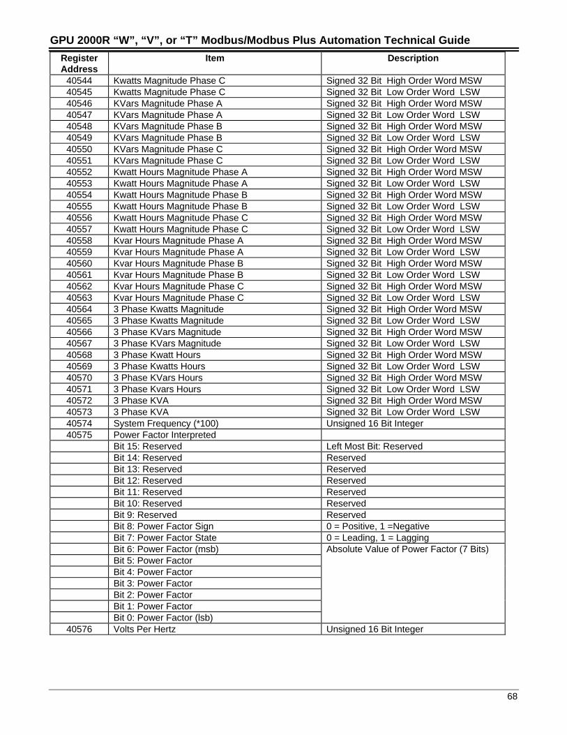
GPU 2000R “W”, “V”, or “T” Modbus/Modbus Plus Automation Technical Guide
68
RegisterAddress
Item Description
40544 Kwatts Magnitude Phase C Signed 32 Bit High Order Word MSW40545 Kwatts Magnitude Phase C Signed 32 Bit Low Order Word LSW40546 KVars Magnitude Phase A Signed 32 Bit High Order Word MSW40547 KVars Magnitude Phase A Signed 32 Bit Low Order Word LSW40548 KVars Magnitude Phase B Signed 32 Bit High Order Word MSW40549 KVars Magnitude Phase B Signed 32 Bit Low Order Word LSW40550 KVars Magnitude Phase C Signed 32 Bit High Order Word MSW40551 KVars Magnitude Phase C Signed 32 Bit Low Order Word LSW40552 Kwatt Hours Magnitude Phase A Signed 32 Bit High Order Word MSW40553 Kwatt Hours Magnitude Phase A Signed 32 Bit Low Order Word LSW40554 Kwatt Hours Magnitude Phase B Signed 32 Bit High Order Word MSW40555 Kwatt Hours Magnitude Phase B Signed 32 Bit Low Order Word LSW40556 Kwatt Hours Magnitude Phase C Signed 32 Bit High Order Word MSW40557 Kwatt Hours Magnitude Phase C Signed 32 Bit Low Order Word LSW40558 Kvar Hours Magnitude Phase A Signed 32 Bit High Order Word MSW40559 Kvar Hours Magnitude Phase A Signed 32 Bit Low Order Word LSW40560 Kvar Hours Magnitude Phase B Signed 32 Bit High Order Word MSW40561 Kvar Hours Magnitude Phase B Signed 32 Bit Low Order Word LSW40562 Kvar Hours Magnitude Phase C Signed 32 Bit High Order Word MSW40563 Kvar Hours Magnitude Phase C Signed 32 Bit Low Order Word LSW40564 3 Phase Kwatts Magnitude Signed 32 Bit High Order Word MSW40565 3 Phase Kwatts Magnitude Signed 32 Bit Low Order Word LSW40566 3 Phase KVars Magnitude Signed 32 Bit High Order Word MSW40567 3 Phase KVars Magnitude Signed 32 Bit Low Order Word LSW40568 3 Phase Kwatt Hours Signed 32 Bit High Order Word MSW40569 3 Phase Kwatts Hours Signed 32 Bit Low Order Word LSW40570 3 Phase KVars Hours Signed 32 Bit High Order Word MSW40571 3 Phase Kvars Hours Signed 32 Bit Low Order Word LSW40572 3 Phase KVA Signed 32 Bit High Order Word MSW40573 3 Phase KVA Signed 32 Bit Low Order Word LSW40574 System Frequency (*100) Unsigned 16 Bit Integer40575 Power Factor Interpreted
Bit 15: Reserved Left Most Bit: ReservedBit 14: Reserved ReservedBit 13: Reserved ReservedBit 12: Reserved ReservedBit 11: Reserved ReservedBit 10: Reserved ReservedBit 9: Reserved ReservedBit 8: Power Factor Sign 0 = Positive, 1 =NegativeBit 7: Power Factor State 0 = Leading, 1 = LaggingBit 6: Power Factor (msb)Bit 5: Power FactorBit 4: Power FactorBit 3: Power FactorBit 2: Power FactorBit 1: Power FactorBit 0: Power Factor (lsb)
Absolute Value of Power Factor (7 Bits)
40576 Volts Per Hertz Unsigned 16 Bit Integer
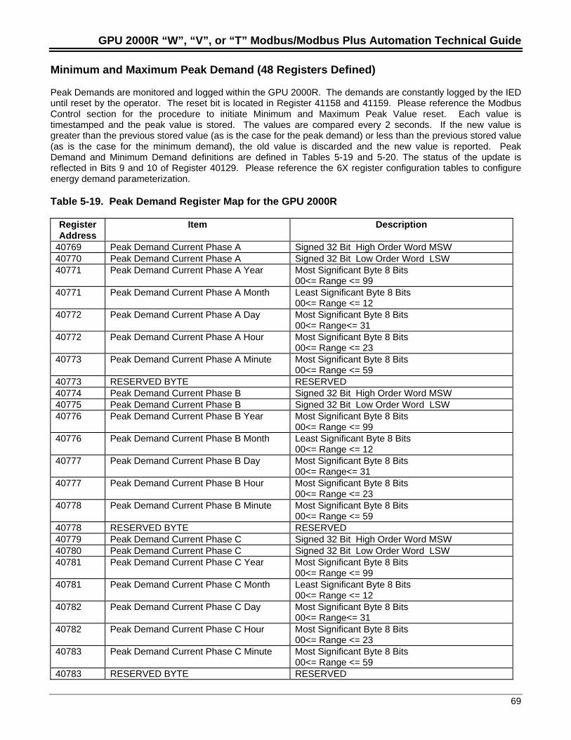
GPU 2000R “W”, “V”, or “T” Modbus/Modbus Plus Automation Technical Guide
69
Minimum and Maximum Peak Demand (48 Registers Defined)
Peak Demands are monitored and logged within the GPU 2000R. The demands are constantly logged by the IEDuntil reset by the operator. The reset bit is located in Register 41158 and 41159. Please reference the ModbusControl section for the procedure to initiate Minimum and Maximum Peak Value reset. Each value istimestamped and the peak value is stored. The values are compared every 2 seconds. If the new value isgreater than the previous stored value (as is the case for the peak demand) or less than the previous stored value(as is the case for the minimum demand), the old value is discarded and the new value is reported. PeakDemand and Minimum Demand definitions are defined in Tables 5-19 and 5-20. The status of the update isreflected in Bits 9 and 10 of Register 40129. Please reference the 6X register configuration tables to configureenergy demand parameterization.
Table 5-19. Peak Demand Register Map for the GPU 2000R
RegisterAddress
Item Description
40769 Peak Demand Current Phase A Signed 32 Bit High Order Word MSW40770 Peak Demand Current Phase A Signed 32 Bit Low Order Word LSW40771 Peak Demand Current Phase A Year Most Significant Byte 8 Bits
00<= Range <= 9940771 Peak Demand Current Phase A Month Least Significant Byte 8 Bits
00<= Range <= 1240772 Peak Demand Current Phase A Day Most Significant Byte 8 Bits
00<= Range<= 3140772 Peak Demand Current Phase A Hour Most Significant Byte 8 Bits
00<= Range <= 2340773 Peak Demand Current Phase A Minute Most Significant Byte 8 Bits
00<= Range <= 5940773 RESERVED BYTE RESERVED40774 Peak Demand Current Phase B Signed 32 Bit High Order Word MSW40775 Peak Demand Current Phase B Signed 32 Bit Low Order Word LSW40776 Peak Demand Current Phase B Year Most Significant Byte 8 Bits
00<= Range <= 9940776 Peak Demand Current Phase B Month Least Significant Byte 8 Bits
00<= Range <= 1240777 Peak Demand Current Phase B Day Most Significant Byte 8 Bits
00<= Range<= 3140777 Peak Demand Current Phase B Hour Most Significant Byte 8 Bits
00<= Range <= 2340778 Peak Demand Current Phase B Minute Most Significant Byte 8 Bits
00<= Range <= 5940778 RESERVED BYTE RESERVED40779 Peak Demand Current Phase C Signed 32 Bit High Order Word MSW40780 Peak Demand Current Phase C Signed 32 Bit Low Order Word LSW40781 Peak Demand Current Phase C Year Most Significant Byte 8 Bits
00<= Range <= 9940781 Peak Demand Current Phase C Month Least Significant Byte 8 Bits
00<= Range <= 1240782 Peak Demand Current Phase C Day Most Significant Byte 8 Bits
00<= Range<= 3140782 Peak Demand Current Phase C Hour Most Significant Byte 8 Bits
00<= Range <= 2340783 Peak Demand Current Phase C Minute Most Significant Byte 8 Bits
00<= Range <= 5940783 RESERVED BYTE RESERVED
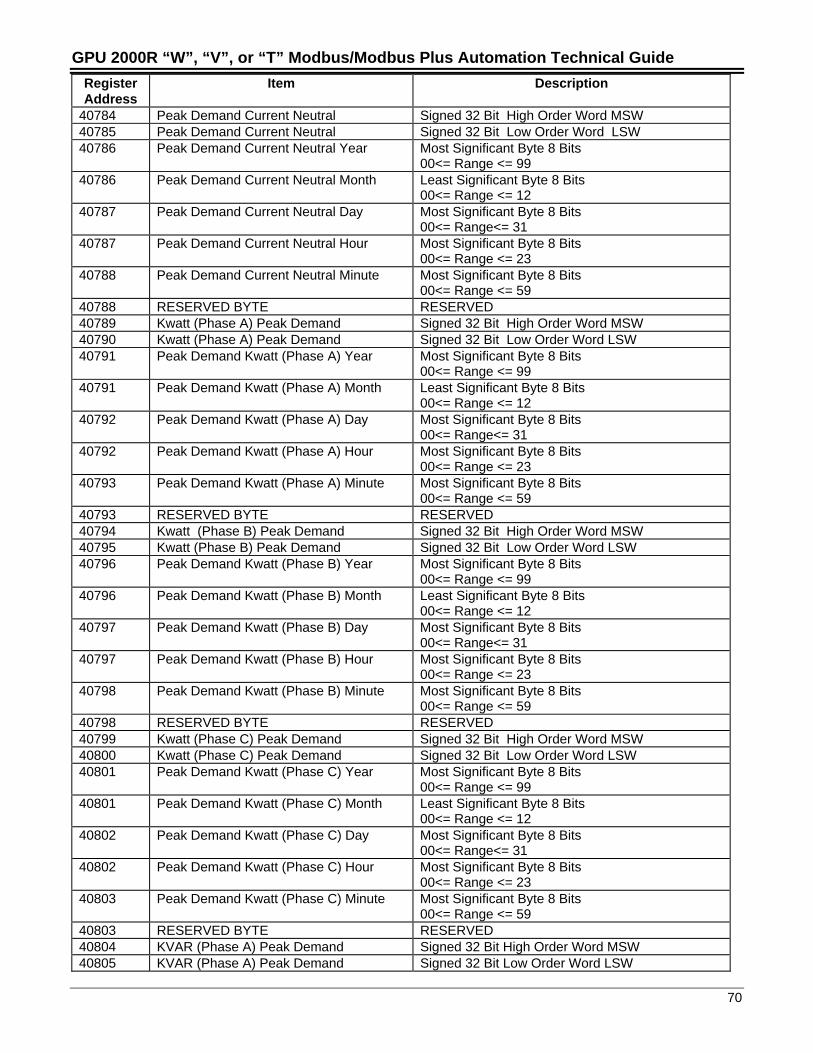
GPU 2000R “W”, “V”, or “T” Modbus/Modbus Plus Automation Technical Guide
70
RegisterAddress
Item Description
40784 Peak Demand Current Neutral Signed 32 Bit High Order Word MSW40785 Peak Demand Current Neutral Signed 32 Bit Low Order Word LSW40786 Peak Demand Current Neutral Year Most Significant Byte 8 Bits
00<= Range <= 9940786 Peak Demand Current Neutral Month Least Significant Byte 8 Bits
00<= Range <= 1240787 Peak Demand Current Neutral Day Most Significant Byte 8 Bits
00<= Range<= 3140787 Peak Demand Current Neutral Hour Most Significant Byte 8 Bits
00<= Range <= 2340788 Peak Demand Current Neutral Minute Most Significant Byte 8 Bits
00<= Range <= 5940788 RESERVED BYTE RESERVED40789 Kwatt (Phase A) Peak Demand Signed 32 Bit High Order Word MSW40790 Kwatt (Phase A) Peak Demand Signed 32 Bit Low Order Word LSW40791 Peak Demand Kwatt (Phase A) Year Most Significant Byte 8 Bits
00<= Range <= 9940791 Peak Demand Kwatt (Phase A) Month Least Significant Byte 8 Bits
00<= Range <= 1240792 Peak Demand Kwatt (Phase A) Day Most Significant Byte 8 Bits
00<= Range<= 3140792 Peak Demand Kwatt (Phase A) Hour Most Significant Byte 8 Bits
00<= Range <= 2340793 Peak Demand Kwatt (Phase A) Minute Most Significant Byte 8 Bits
00<= Range <= 5940793 RESERVED BYTE RESERVED40794 Kwatt (Phase B) Peak Demand Signed 32 Bit High Order Word MSW40795 Kwatt (Phase B) Peak Demand Signed 32 Bit Low Order Word LSW40796 Peak Demand Kwatt (Phase B) Year Most Significant Byte 8 Bits
00<= Range <= 9940796 Peak Demand Kwatt (Phase B) Month Least Significant Byte 8 Bits
00<= Range <= 1240797 Peak Demand Kwatt (Phase B) Day Most Significant Byte 8 Bits
00<= Range<= 3140797 Peak Demand Kwatt (Phase B) Hour Most Significant Byte 8 Bits
00<= Range <= 2340798 Peak Demand Kwatt (Phase B) Minute Most Significant Byte 8 Bits
00<= Range <= 5940798 RESERVED BYTE RESERVED40799 Kwatt (Phase C) Peak Demand Signed 32 Bit High Order Word MSW40800 Kwatt (Phase C) Peak Demand Signed 32 Bit Low Order Word LSW40801 Peak Demand Kwatt (Phase C) Year Most Significant Byte 8 Bits
00<= Range <= 9940801 Peak Demand Kwatt (Phase C) Month Least Significant Byte 8 Bits
00<= Range <= 1240802 Peak Demand Kwatt (Phase C) Day Most Significant Byte 8 Bits
00<= Range<= 3140802 Peak Demand Kwatt (Phase C) Hour Most Significant Byte 8 Bits
00<= Range <= 2340803 Peak Demand Kwatt (Phase C) Minute Most Significant Byte 8 Bits
00<= Range <= 5940803 RESERVED BYTE RESERVED40804 KVAR (Phase A) Peak Demand Signed 32 Bit High Order Word MSW40805 KVAR (Phase A) Peak Demand Signed 32 Bit Low Order Word LSW
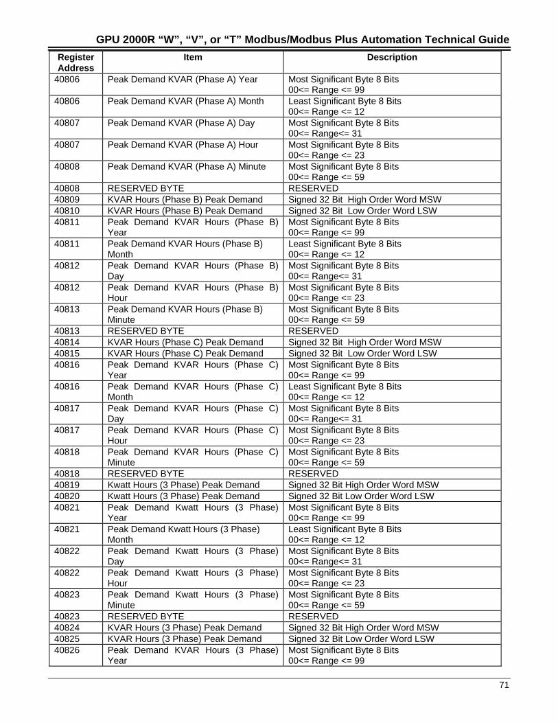
GPU 2000R “W”, “V”, or “T” Modbus/Modbus Plus Automation Technical Guide
71
RegisterAddress
Item Description
40806 Peak Demand KVAR (Phase A) Year Most Significant Byte 8 Bits00<= Range <= 99
40806 Peak Demand KVAR (Phase A) Month Least Significant Byte 8 Bits00<= Range <= 12
40807 Peak Demand KVAR (Phase A) Day Most Significant Byte 8 Bits00<= Range<= 31
40807 Peak Demand KVAR (Phase A) Hour Most Significant Byte 8 Bits00<= Range <= 23
40808 Peak Demand KVAR (Phase A) Minute Most Significant Byte 8 Bits00<= Range <= 59
40808 RESERVED BYTE RESERVED40809 KVAR Hours (Phase B) Peak Demand Signed 32 Bit High Order Word MSW40810 KVAR Hours (Phase B) Peak Demand Signed 32 Bit Low Order Word LSW40811 Peak Demand KVAR Hours (Phase B)
YearMost Significant Byte 8 Bits00<= Range <= 99
40811 Peak Demand KVAR Hours (Phase B)Month
Least Significant Byte 8 Bits00<= Range <= 12
40812 Peak Demand KVAR Hours (Phase B)Day
Most Significant Byte 8 Bits00<= Range<= 31
40812 Peak Demand KVAR Hours (Phase B)Hour
Most Significant Byte 8 Bits00<= Range <= 23
40813 Peak Demand KVAR Hours (Phase B)Minute
Most Significant Byte 8 Bits00<= Range <= 59
40813 RESERVED BYTE RESERVED40814 KVAR Hours (Phase C) Peak Demand Signed 32 Bit High Order Word MSW40815 KVAR Hours (Phase C) Peak Demand Signed 32 Bit Low Order Word LSW40816 Peak Demand KVAR Hours (Phase C)
YearMost Significant Byte 8 Bits00<= Range <= 99
40816 Peak Demand KVAR Hours (Phase C)Month
Least Significant Byte 8 Bits00<= Range <= 12
40817 Peak Demand KVAR Hours (Phase C)Day
Most Significant Byte 8 Bits00<= Range<= 31
40817 Peak Demand KVAR Hours (Phase C)Hour
Most Significant Byte 8 Bits00<= Range <= 23
40818 Peak Demand KVAR Hours (Phase C)Minute
Most Significant Byte 8 Bits00<= Range <= 59
40818 RESERVED BYTE RESERVED40819 Kwatt Hours (3 Phase) Peak Demand Signed 32 Bit High Order Word MSW40820 Kwatt Hours (3 Phase) Peak Demand Signed 32 Bit Low Order Word LSW40821 Peak Demand Kwatt Hours (3 Phase)
YearMost Significant Byte 8 Bits00<= Range <= 99
40821 Peak Demand Kwatt Hours (3 Phase)Month
Least Significant Byte 8 Bits00<= Range <= 12
40822 Peak Demand Kwatt Hours (3 Phase)Day
Most Significant Byte 8 Bits00<= Range<= 31
40822 Peak Demand Kwatt Hours (3 Phase)Hour
Most Significant Byte 8 Bits00<= Range <= 23
40823 Peak Demand Kwatt Hours (3 Phase)Minute
Most Significant Byte 8 Bits00<= Range <= 59
40823 RESERVED BYTE RESERVED40824 KVAR Hours (3 Phase) Peak Demand Signed 32 Bit High Order Word MSW40825 KVAR Hours (3 Phase) Peak Demand Signed 32 Bit Low Order Word LSW40826 Peak Demand KVAR Hours (3 Phase)
YearMost Significant Byte 8 Bits00<= Range <= 99
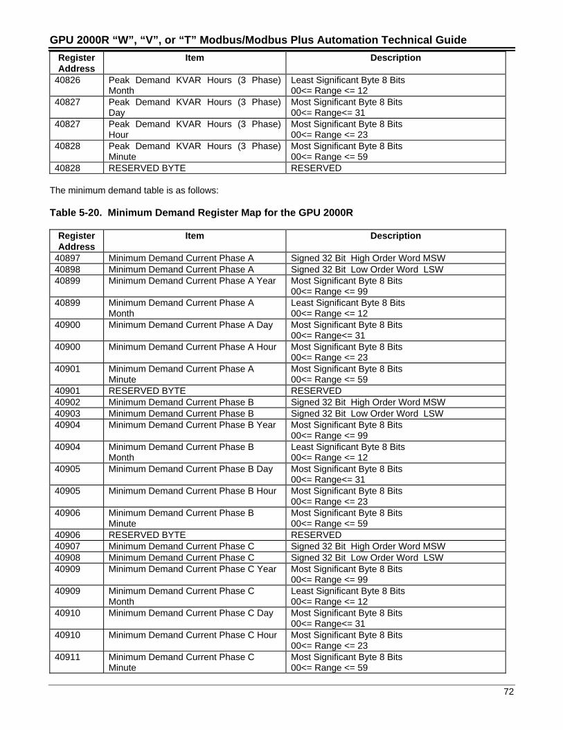
GPU 2000R “W”, “V”, or “T” Modbus/Modbus Plus Automation Technical Guide
72
RegisterAddress
Item Description
40826 Peak Demand KVAR Hours (3 Phase)Month
Least Significant Byte 8 Bits00<= Range <= 12
40827 Peak Demand KVAR Hours (3 Phase)Day
Most Significant Byte 8 Bits00<= Range<= 31
40827 Peak Demand KVAR Hours (3 Phase)Hour
Most Significant Byte 8 Bits00<= Range <= 23
40828 Peak Demand KVAR Hours (3 Phase)Minute
Most Significant Byte 8 Bits00<= Range <= 59
40828 RESERVED BYTE RESERVED
The minimum demand table is as follows:
Table 5-20. Minimum Demand Register Map for the GPU 2000R
RegisterAddress
Item Description
40897 Minimum Demand Current Phase A Signed 32 Bit High Order Word MSW40898 Minimum Demand Current Phase A Signed 32 Bit Low Order Word LSW40899 Minimum Demand Current Phase A Year Most Significant Byte 8 Bits
00<= Range <= 9940899 Minimum Demand Current Phase A
MonthLeast Significant Byte 8 Bits00<= Range <= 12
40900 Minimum Demand Current Phase A Day Most Significant Byte 8 Bits00<= Range<= 31
40900 Minimum Demand Current Phase A Hour Most Significant Byte 8 Bits00<= Range <= 23
40901 Minimum Demand Current Phase AMinute
Most Significant Byte 8 Bits00<= Range <= 59
40901 RESERVED BYTE RESERVED40902 Minimum Demand Current Phase B Signed 32 Bit High Order Word MSW40903 Minimum Demand Current Phase B Signed 32 Bit Low Order Word LSW40904 Minimum Demand Current Phase B Year Most Significant Byte 8 Bits
00<= Range <= 9940904 Minimum Demand Current Phase B
MonthLeast Significant Byte 8 Bits00<= Range <= 12
40905 Minimum Demand Current Phase B Day Most Significant Byte 8 Bits00<= Range<= 31
40905 Minimum Demand Current Phase B Hour Most Significant Byte 8 Bits00<= Range <= 23
40906 Minimum Demand Current Phase BMinute
Most Significant Byte 8 Bits00<= Range <= 59
40906 RESERVED BYTE RESERVED40907 Minimum Demand Current Phase C Signed 32 Bit High Order Word MSW40908 Minimum Demand Current Phase C Signed 32 Bit Low Order Word LSW40909 Minimum Demand Current Phase C Year Most Significant Byte 8 Bits
00<= Range <= 9940909 Minimum Demand Current Phase C
MonthLeast Significant Byte 8 Bits00<= Range <= 12
40910 Minimum Demand Current Phase C Day Most Significant Byte 8 Bits00<= Range<= 31
40910 Minimum Demand Current Phase C Hour Most Significant Byte 8 Bits00<= Range <= 23
40911 Minimum Demand Current Phase CMinute
Most Significant Byte 8 Bits00<= Range <= 59
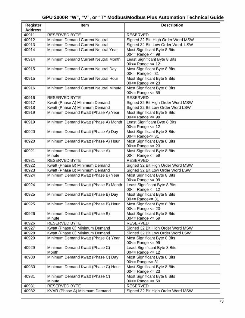
GPU 2000R “W”, “V”, or “T” Modbus/Modbus Plus Automation Technical Guide
73
RegisterAddress
Item Description
40911 RESERVED BYTE RESERVED40912 Minimum Demand Current Neutral Signed 32 Bit High Order Word MSW40913 Minimum Demand Current Neutral Signed 32 Bit Low Order Word LSW40914 Minimum Demand Current Neutral Year Most Significant Byte 8 Bits
00<= Range <= 9940914 Minimum Demand Current Neutral Month Least Significant Byte 8 Bits
00<= Range <= 1240915 Minimum Demand Current Neutral Day Most Significant Byte 8 Bits
00<= Range<= 3140915 Minimum Demand Current Neutral Hour Most Significant Byte 8 Bits
00<= Range <= 2340916 Minimum Demand Current Neutral Minute Most Significant Byte 8 Bits
00<= Range <= 5940916 RESERVED BYTE RESERVED40917 Kwatt (Phase A) Minimum Demand Signed 32 Bit High Order Word MSW40918 Kwatt (Phase A) Minimum Demand Signed 32 Bit Low Order Word LSW40919 Minimum Demand Kwatt (Phase A) Year Most Significant Byte 8 Bits
00<= Range <= 9940919 Minimum Demand Kwatt (Phase A) Month Least Significant Byte 8 Bits
00<= Range <= 1240920 Minimum Demand Kwatt (Phase A) Day Most Significant Byte 8 Bits
00<= Range<= 3140920 Minimum Demand Kwatt (Phase A) Hour Most Significant Byte 8 Bits
00<= Range <= 2340921 Minimum Demand Kwatt (Phase A)
MinuteMost Significant Byte 8 Bits00<= Range <= 59
40921 RESERVED BYTE RESERVED40922 Kwatt (Phase B) Minimum Demand Signed 32 Bit High Order Word MSW40923 Kwatt (Phase B) Minimum Demand Signed 32 Bit Low Order Word LSW40924 Minimum Demand Kwatt (Phase B) Year Most Significant Byte 8 Bits
00<= Range <= 9940924 Minimum Demand Kwatt (Phase B) Month Least Significant Byte 8 Bits
00<= Range <= 1240925 Minimum Demand Kwatt (Phase B) Day Most Significant Byte 8 Bits
00<= Range<= 3140925 Minimum Demand Kwatt (Phase B) Hour Most Significant Byte 8 Bits
00<= Range <= 2340926 Minimum Demand Kwatt (Phase B)
MinuteMost Significant Byte 8 Bits00<= Range <= 59
40926 RESERVED BYTE RESERVED40927 Kwatt (Phase C) Minimum Demand Signed 32 Bit High Order Word MSW40928 Kwatt (Phase C) Minimum Demand Signed 32 Bit Low Order Word LSW40929 Minimum Demand Kwatt (Phase C) Year Most Significant Byte 8 Bits
00<= Range <= 9940929 Minimum Demand Kwatt (Phase C)
MonthLeast Significant Byte 8 Bits00<= Range <= 12
40930 Minimum Demand Kwatt (Phase C) Day Most Significant Byte 8 Bits00<= Range<= 31
40930 Minimum Demand Kwatt (Phase C) Hour Most Significant Byte 8 Bits00<= Range <= 23
40931 Minimum Demand Kwatt (Phase C)Minute
Most Significant Byte 8 Bits00<= Range <= 59
40931 RESERVED BYTE RESERVED40932 KVAR (Phase A) Minimum Demand Signed 32 Bit High Order Word MSW
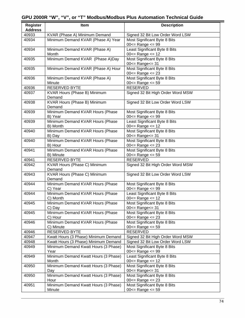
GPU 2000R “W”, “V”, or “T” Modbus/Modbus Plus Automation Technical Guide
74
RegisterAddress
Item Description
40933 KVAR (Phase A) Minimum Demand Signed 32 Bit Low Order Word LSW40934 Minimum Demand KVAR (Phase A) Year Most Significant Byte 8 Bits
00<= Range <= 9940934 Minimum Demand KVAR (Phase A)
MonthLeast Significant Byte 8 Bits00<= Range <= 12
40935 Minimum Demand KVAR (Phase A)Day Most Significant Byte 8 Bits00<= Range<= 31
40935 Minimum Demand KVAR (Phase A) Hour Most Significant Byte 8 Bits00<= Range <= 23
40936 Minimum Demand KVAR (Phase A)Minute
Most Significant Byte 8 Bits00<= Range <= 59
40936 RESERVED BYTE RESERVED40937 KVAR Hours (Phase B) Minimum
DemandSigned 32 Bit High Order Word MSW
40938 KVAR Hours (Phase B) MinimumDemand
Signed 32 Bit Low Order Word LSW
40939 Minimum Demand KVAR Hours (PhaseB) Year
Most Significant Byte 8 Bits00<= Range <= 99
40939 Minimum Demand KVAR Hours (PhaseB) Month
Least Significant Byte 8 Bits00<= Range <= 12
40940 Minimum Demand KVAR Hours (PhaseB) Day
Most Significant Byte 8 Bits00<= Range<= 31
40940 Minimum Demand KVAR Hours (PhaseB) Hour
Most Significant Byte 8 Bits00<= Range <= 23
40941 Minimum Demand KVAR Hours (PhaseB) Minute
Most Significant Byte 8 Bits00<= Range <= 59
40941 RESERVED BYTE RESERVED40942 KVAR Hours (Phase C) Minimum
DemandSigned 32 Bit High Order Word MSW
40943 KVAR Hours (Phase C) MinimumDemand
Signed 32 Bit Low Order Word LSW
40944 Minimum Demand KVAR Hours (PhaseC) Year
Most Significant Byte 8 Bits00<= Range <= 99
40944 Minimum Demand KVAR Hours (PhaseC) Month
Least Significant Byte 8 Bits00<= Range <= 12
40945 Minimum Demand KVAR Hours (PhaseC) Day
Most Significant Byte 8 Bits00<= Range<= 31
40945 Minimum Demand KVAR Hours (PhaseC) Hour
Most Significant Byte 8 Bits00<= Range <= 23
40946 Minimum Demand KVAR Hours (PhaseC) Minute
Most Significant Byte 8 Bits00<= Range <= 59
40946 RESERVED BYTE RESERVED40947 Kwatt Hours (3 Phase) Minimum Demand Signed 32 Bit High Order Word MSW40948 Kwatt Hours (3 Phase) Minimum Demand Signed 32 Bit Low Order Word LSW40949 Minimum Demand Kwatt Hours (3 Phase)
YearMost Significant Byte 8 Bits00<= Range <= 99
40949 Minimum Demand Kwatt Hours (3 Phase)Month
Least Significant Byte 8 Bits00<= Range <= 12
40950 Minimum Demand Kwatt Hours (3 Phase)Day
Most Significant Byte 8 Bits00<= Range<= 31
40950 Minimum Demand Kwatt Hours (3 Phase)Hour
Most Significant Byte 8 Bits00<= Range <= 23
40951 Minimum Demand Kwatt Hours (3 Phase)Minute
Most Significant Byte 8 Bits00<= Range <= 59
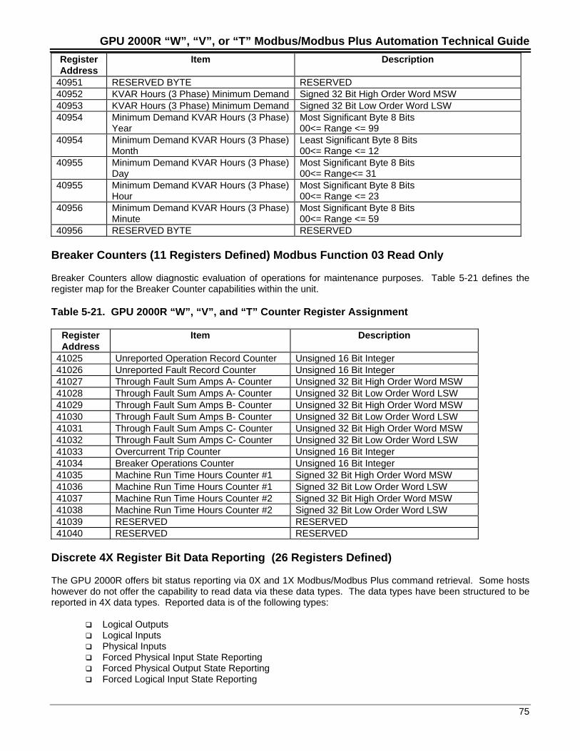
GPU 2000R “W”, “V”, or “T” Modbus/Modbus Plus Automation Technical Guide
75
RegisterAddress
Item Description
40951 RESERVED BYTE RESERVED40952 KVAR Hours (3 Phase) Minimum Demand Signed 32 Bit High Order Word MSW40953 KVAR Hours (3 Phase) Minimum Demand Signed 32 Bit Low Order Word LSW40954 Minimum Demand KVAR Hours (3 Phase)
YearMost Significant Byte 8 Bits00<= Range <= 99
40954 Minimum Demand KVAR Hours (3 Phase)Month
Least Significant Byte 8 Bits00<= Range <= 12
40955 Minimum Demand KVAR Hours (3 Phase)Day
Most Significant Byte 8 Bits00<= Range<= 31
40955 Minimum Demand KVAR Hours (3 Phase)Hour
Most Significant Byte 8 Bits00<= Range <= 23
40956 Minimum Demand KVAR Hours (3 Phase)Minute
Most Significant Byte 8 Bits00<= Range <= 59
40956 RESERVED BYTE RESERVED
Breaker Counters (11 Registers Defined) Modbus Function 03 Read Only
Breaker Counters allow diagnostic evaluation of operations for maintenance purposes. Table 5-21 defines theregister map for the Breaker Counter capabilities within the unit.
Table 5-21. GPU 2000R “W”, “V”, and “T” Counter Register Assignment
RegisterAddress
Item Description
41025 Unreported Operation Record Counter Unsigned 16 Bit Integer41026 Unreported Fault Record Counter Unsigned 16 Bit Integer41027 Through Fault Sum Amps A- Counter Unsigned 32 Bit High Order Word MSW41028 Through Fault Sum Amps A- Counter Unsigned 32 Bit Low Order Word LSW41029 Through Fault Sum Amps B- Counter Unsigned 32 Bit High Order Word MSW41030 Through Fault Sum Amps B- Counter Unsigned 32 Bit Low Order Word LSW41031 Through Fault Sum Amps C- Counter Unsigned 32 Bit High Order Word MSW41032 Through Fault Sum Amps C- Counter Unsigned 32 Bit Low Order Word LSW41033 Overcurrent Trip Counter Unsigned 16 Bit Integer41034 Breaker Operations Counter Unsigned 16 Bit Integer41035 Machine Run Time Hours Counter #1 Signed 32 Bit High Order Word MSW41036 Machine Run Time Hours Counter #1 Signed 32 Bit Low Order Word LSW41037 Machine Run Time Hours Counter #2 Signed 32 Bit High Order Word MSW41038 Machine Run Time Hours Counter #2 Signed 32 Bit Low Order Word LSW41039 RESERVED RESERVED41040 RESERVED RESERVED
Discrete 4X Register Bit Data Reporting (26 Registers Defined)
The GPU 2000R offers bit status reporting via 0X and 1X Modbus/Modbus Plus command retrieval. Some hostshowever do not offer the capability to read data via these data types. The data types have been structured to bereported in 4X data types. Reported data is of the following types:
Logical Outputs Logical Inputs Physical Inputs Forced Physical Input State Reporting Forced Physical Output State Reporting Forced Logical Input State Reporting
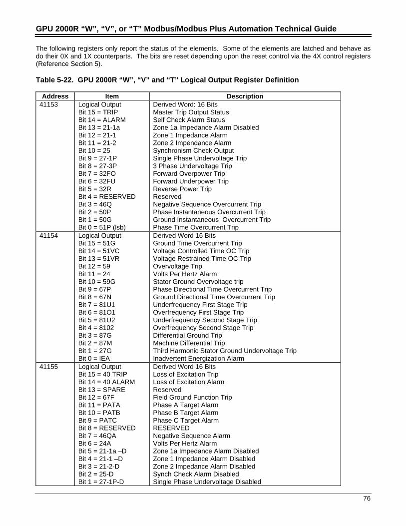
GPU 2000R “W”, “V”, or “T” Modbus/Modbus Plus Automation Technical Guide
76
The following registers only report the status of the elements. Some of the elements are latched and behave asdo their 0X and 1X counterparts. The bits are reset depending upon the reset control via the 4X control registers(Reference Section 5).
Table 5-22. GPU 2000R “W”, “V” and “T” Logical Output Register Definition
Address Item Description41153 Logical Output
Bit 15 = TRIPBit 14 = ALARMBit 13 = 21-1aBit 12 = 21-1Bit 11 = 21-2Bit 10 = 25Bit 9 = 27-1PBit 8 = 27-3PBit 7 = 32FOBit 6 = 32FUBit 5 = 32RBit 4 = RESERVEDBit 3 = 46QBit 2 = 50PBit 1 = 50GBit 0 = 51P (lsb)
Derived Word: 16 BitsMaster Trip Output StatusSelf Check Alarm StatusZone 1a Impedance Alarm DisabledZone 1 Impedance AlarmZone 2 Impendance AlarmSynchronism Check OutputSingle Phase Undervoltage Trip3 Phase Undervoltage TripForward Overpower TripForward Underpower TripReverse Power TripReservedNegative Sequence Overcurrent TripPhase Instantaneous Overcurrent TripGround Instantaneous Overcurrent TripPhase Time Overcurrent Trip
41154 Logical OutputBit 15 = 51GBit 14 = 51VCBit 13 = 51VRBit 12 = 59Bit 11 = 24Bit 10 = 59GBit 9 = 67PBit 8 = 67NBit 7 = 81U1Bit 6 = 81O1Bit 5 = 81U2Bit 4 = 8102Bit 3 = 87GBit 2 = 87MBit 1 = 27GBit 0 = IEA
Derived Word 16 BitsGround Time Overcurrent TripVoltage Controlled Time OC TripVoltage Restrained Time OC TripOvervoltage TripVolts Per Hertz AlarmStator Ground Overvoltage tripPhase Directional Time Overcurrent TripGround Directional Time Overcurrent TripUnderfrequency First Stage TripOverfrequency First Stage TripUnderfrequency Second Stage TripOverfrequency Second Stage TripDifferential Ground TripMachine Differential TripThird Harmonic Stator Ground Undervoltage TripInadvertent Energization Alarm
41155 Logical OutputBit 15 = 40 TRIPBit 14 = 40 ALARMBit 13 = SPAREBit 12 = 67FBit 11 = PATABit 10 = PATBBit 9 = PATCBit 8 = RESERVEDBit 7 = 46QABit 6 = 24ABit 5 = 21-1a –DBit 4 = 21-1 –DBit 3 = 21-2-DBit 2 = 25-DBit 1 = 27-1P-D
Derived Word 16 BitsLoss of Excitation TripLoss of Excitation AlarmReservedField Ground Function TripPhase A Target AlarmPhase B Target AlarmPhase C Target AlarmRESERVEDNegative Sequence AlarmVolts Per Hertz AlarmZone 1a Impedance Alarm DisabledZone 1 Impedance Alarm DisabledZone 2 Impedance Alarm DisabledSynch Check Alarm DisabledSingle Phase Undervoltage Disabled
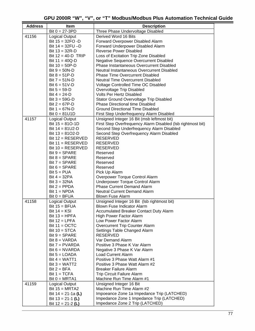
GPU 2000R “W”, “V”, or “T” Modbus/Modbus Plus Automation Technical Guide
77
Address Item DescriptionBit 0 = 27-3PD Three Phase Undervoltage Disabled
41156 Logical OutputBit 15 = 32FO -DBit 14 = 32FU –DBit 13 = 32R-DBit 12 = 40-D TRIPBit 11 = 40Q-DBit 10 = 50P-DBit 9 = 50N-DBit 8 = 51P-DBit 7 = 51N-DBit 6 = 51V-DBit 5 = 59-DBit 4 = 24-DBit 3 = 59G-DBit 2 = 67P-DBit 1 = 67N-DBit 0 = 81U1D
Derived Word 16 BitsForward Overpower Disabled AlarmForward Underpower Disabled AlarmReverse Power DisabledLoss of Excitation Trip Zone DisabledNegative Sequence Overcurrent DisabledPhase Instantaneous Overcurrent DisabledNeutral Instantaneous Overcurrent DisabledPhase Time Overcurrent DisabledNeutral Time Overcurrent DisabledVoltage Controlled Time OC DisabledOvervoltage Trip DisabledVolts Per Hertz DisabledStator Ground Overvoltage Trip DisabledPhase Directional time DisabledGround Directional Time DisabledFirst Step Underfrequency Alarm Disabled
41157 Logical OutputBit 15 = 81O-1DBit 14 = 81U2-DBit 13 = 81O2-DBit 12 = RESERVEDBit 11 = RESERVEDBit 10 = RESERVEDBit 9 = SPAREBit 8 = SPAREBit 7 = SPAREBit 6 = SPAREBit 5 = PUABit 4 = 32PABit 3 = 32NABit 2 = PPDABit 1 = NPDABit 0 = BFUA
Unsigned Integer 16 Bit (msb leftmost bit)First Step Overfrequency Alarm Disabled (lsb rightmost bit)Second Step Underfrequency Alarm DisabledSecond Step Overfrequency Alarm DisabledRESERVEDRESERVEDRESERVEDReservedReservedReservedReservedPick Up AlarmOverpower Torque Control AlarmUnderpower Torque Control AlarmPhase Current Demand AlarmNeutral Current Demand AlarmBlown Fuse Alarm
41158 Logical OutputBit 15 = BFUABit 14 = KSIBit 13 = HPFABit 12 = LPFABit 11 = OCTCBit 10 = STCABit 9 = SPAREBit 8 = VARDABit 7 = PVARDABit 6 = NVARDABit 5 = LOADABit 4 = WATT1Bit 3 = WATT2Bit 2 = BFABit 1 = TCFABit 0 = MRTA1
Unsigned Integer 16 Bit (lsb rightmost bit)Blown Fuse Indicator AlarmAccumulated Breaker Contact Duty AlarmHigh Power Factor AlarmLow Power Factor AlarmOvercurrent Trip Counter AlarmSettings Table Changed AlarmRESERVEDVar Demand AlarmPositive 3 Phase K Var AlarmNegative 3 Phase K Var AlarmLoad Current AlarmPositive 3 Phase Watt Alarm #1Positive 3 Phase Watt Alarm #2Breaker Failure AlarmTrip Circuit Failure AlarmMachine Run Time Alarm #1
41159 Logical OutputBit 15 = MRTA2Bit 14 = 21-1a (L)Bit 13 = 21-1 (L)Bit 12 = 21-2 (L)
Unsigned Integer 16 BitMachine Run Time Alarm #2Impoeance Zone 1a Impedance Trip (LATCHED)Impedance Zone 1 Impedance Trip (LATCHED)Impedance Zone 2 Trip (LATCHED)
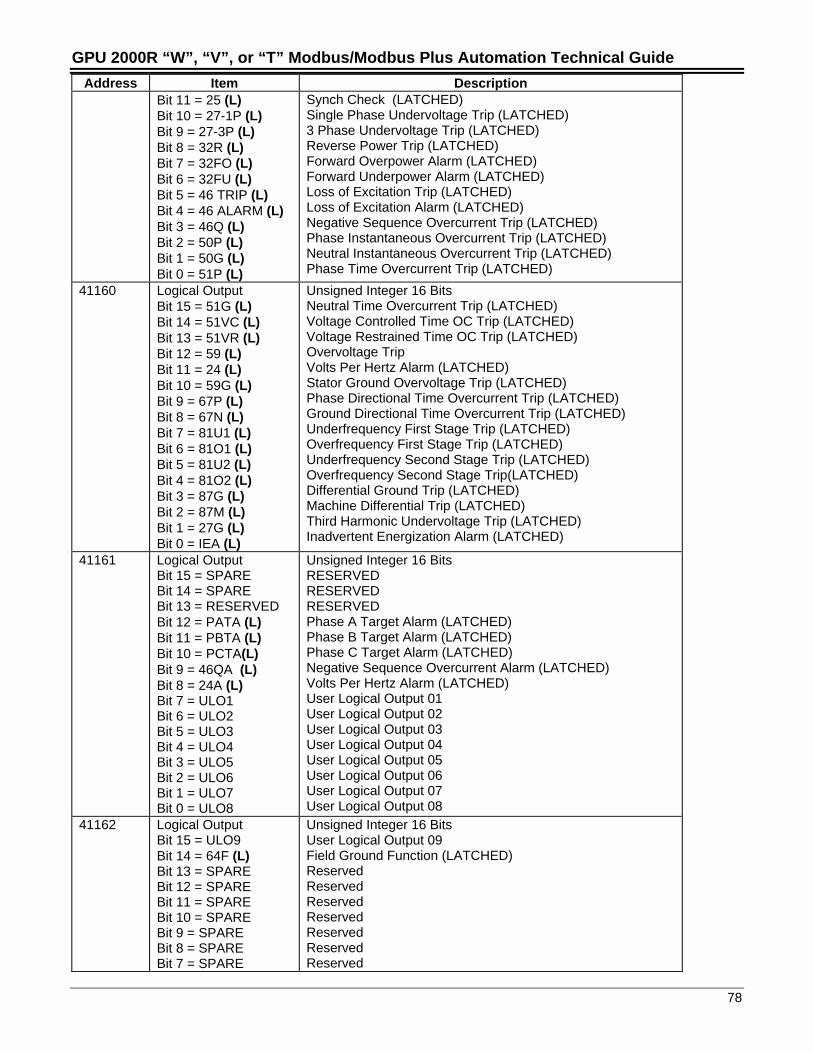
GPU 2000R “W”, “V”, or “T” Modbus/Modbus Plus Automation Technical Guide
78
Address Item DescriptionBit 11 = 25 (L)Bit 10 = 27-1P (L)Bit 9 = 27-3P (L)Bit 8 = 32R (L)Bit 7 = 32FO (L)Bit 6 = 32FU (L)Bit 5 = 46 TRIP (L)Bit 4 = 46 ALARM (L)Bit 3 = 46Q (L)Bit 2 = 50P (L)Bit 1 = 50G (L)Bit 0 = 51P (L)
Synch Check (LATCHED)Single Phase Undervoltage Trip (LATCHED)3 Phase Undervoltage Trip (LATCHED)Reverse Power Trip (LATCHED)Forward Overpower Alarm (LATCHED)Forward Underpower Alarm (LATCHED)Loss of Excitation Trip (LATCHED)Loss of Excitation Alarm (LATCHED)Negative Sequence Overcurrent Trip (LATCHED)Phase Instantaneous Overcurrent Trip (LATCHED)Neutral Instantaneous Overcurrent Trip (LATCHED)Phase Time Overcurrent Trip (LATCHED)
41160 Logical OutputBit 15 = 51G (L)Bit 14 = 51VC (L)Bit 13 = 51VR (L)Bit 12 = 59 (L)Bit 11 = 24 (L)Bit 10 = 59G (L)Bit 9 = 67P (L)Bit 8 = 67N (L)Bit 7 = 81U1 (L)Bit 6 = 81O1 (L)Bit 5 = 81U2 (L)Bit 4 = 81O2 (L)Bit 3 = 87G (L)Bit 2 = 87M (L)Bit 1 = 27G (L)Bit 0 = IEA (L)
Unsigned Integer 16 BitsNeutral Time Overcurrent Trip (LATCHED)Voltage Controlled Time OC Trip (LATCHED)Voltage Restrained Time OC Trip (LATCHED)Overvoltage TripVolts Per Hertz Alarm (LATCHED)Stator Ground Overvoltage Trip (LATCHED)Phase Directional Time Overcurrent Trip (LATCHED)Ground Directional Time Overcurrent Trip (LATCHED)Underfrequency First Stage Trip (LATCHED)Overfrequency First Stage Trip (LATCHED)Underfrequency Second Stage Trip (LATCHED)Overfrequency Second Stage Trip(LATCHED)Differential Ground Trip (LATCHED)Machine Differential Trip (LATCHED)Third Harmonic Undervoltage Trip (LATCHED)Inadvertent Energization Alarm (LATCHED)
41161 Logical OutputBit 15 = SPAREBit 14 = SPAREBit 13 = RESERVEDBit 12 = PATA (L)Bit 11 = PBTA (L)Bit 10 = PCTA(L)Bit 9 = 46QA (L)Bit 8 = 24A (L)Bit 7 = ULO1Bit 6 = ULO2Bit 5 = ULO3Bit 4 = ULO4Bit 3 = ULO5Bit 2 = ULO6Bit 1 = ULO7Bit 0 = ULO8
Unsigned Integer 16 BitsRESERVEDRESERVEDRESERVEDPhase A Target Alarm (LATCHED)Phase B Target Alarm (LATCHED)Phase C Target Alarm (LATCHED)Negative Sequence Overcurrent Alarm (LATCHED)Volts Per Hertz Alarm (LATCHED)User Logical Output 01User Logical Output 02User Logical Output 03User Logical Output 04User Logical Output 05User Logical Output 06User Logical Output 07User Logical Output 08
41162 Logical OutputBit 15 = ULO9Bit 14 = 64F (L)Bit 13 = SPAREBit 12 = SPAREBit 11 = SPAREBit 10 = SPAREBit 9 = SPAREBit 8 = SPAREBit 7 = SPARE
Unsigned Integer 16 BitsUser Logical Output 09Field Ground Function (LATCHED)ReservedReservedReservedReservedReservedReservedReserved
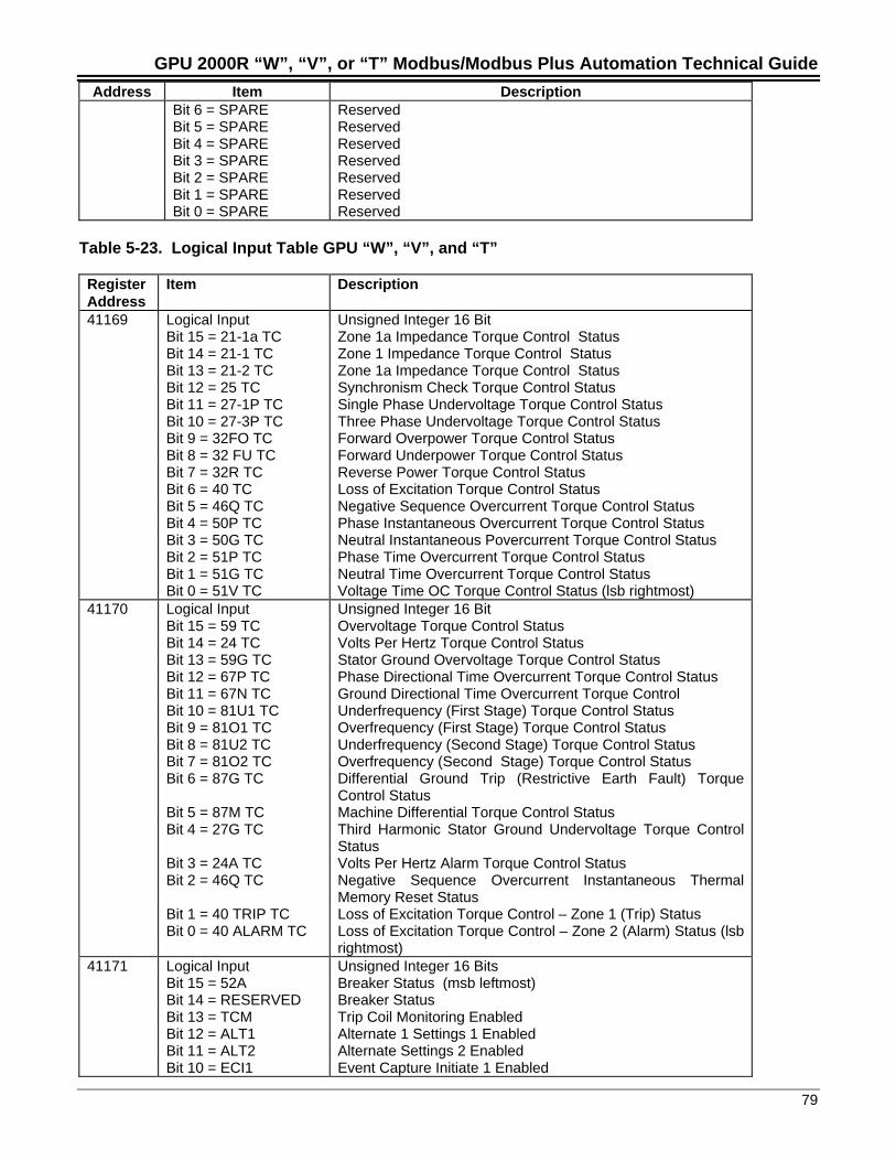
GPU 2000R “W”, “V”, or “T” Modbus/Modbus Plus Automation Technical Guide
79
Address Item DescriptionBit 6 = SPAREBit 5 = SPAREBit 4 = SPAREBit 3 = SPAREBit 2 = SPAREBit 1 = SPAREBit 0 = SPARE
ReservedReservedReservedReservedReservedReservedReserved
Table 5-23. Logical Input Table GPU “W”, “V”, and “T”
RegisterAddress
Item Description
41169 Logical InputBit 15 = 21-1a TCBit 14 = 21-1 TCBit 13 = 21-2 TCBit 12 = 25 TCBit 11 = 27-1P TCBit 10 = 27-3P TCBit 9 = 32FO TCBit 8 = 32 FU TCBit 7 = 32R TCBit 6 = 40 TCBit 5 = 46Q TCBit 4 = 50P TCBit 3 = 50G TCBit 2 = 51P TCBit 1 = 51G TCBit 0 = 51V TC
Unsigned Integer 16 BitZone 1a Impedance Torque Control StatusZone 1 Impedance Torque Control StatusZone 1a Impedance Torque Control StatusSynchronism Check Torque Control StatusSingle Phase Undervoltage Torque Control StatusThree Phase Undervoltage Torque Control StatusForward Overpower Torque Control StatusForward Underpower Torque Control StatusReverse Power Torque Control StatusLoss of Excitation Torque Control StatusNegative Sequence Overcurrent Torque Control StatusPhase Instantaneous Overcurrent Torque Control StatusNeutral Instantaneous Povercurrent Torque Control StatusPhase Time Overcurrent Torque Control StatusNeutral Time Overcurrent Torque Control StatusVoltage Time OC Torque Control Status (lsb rightmost)
41170 Logical InputBit 15 = 59 TCBit 14 = 24 TCBit 13 = 59G TCBit 12 = 67P TCBit 11 = 67N TCBit 10 = 81U1 TCBit 9 = 81O1 TCBit 8 = 81U2 TCBit 7 = 81O2 TCBit 6 = 87G TC
Bit 5 = 87M TCBit 4 = 27G TC
Bit 3 = 24A TCBit 2 = 46Q TC
Bit 1 = 40 TRIP TCBit 0 = 40 ALARM TC
Unsigned Integer 16 BitOvervoltage Torque Control StatusVolts Per Hertz Torque Control StatusStator Ground Overvoltage Torque Control StatusPhase Directional Time Overcurrent Torque Control StatusGround Directional Time Overcurrent Torque ControlUnderfrequency (First Stage) Torque Control StatusOverfrequency (First Stage) Torque Control StatusUnderfrequency (Second Stage) Torque Control StatusOverfrequency (Second Stage) Torque Control StatusDifferential Ground Trip (Restrictive Earth Fault) TorqueControl StatusMachine Differential Torque Control StatusThird Harmonic Stator Ground Undervoltage Torque ControlStatusVolts Per Hertz Alarm Torque Control StatusNegative Sequence Overcurrent Instantaneous ThermalMemory Reset StatusLoss of Excitation Torque Control – Zone 1 (Trip) StatusLoss of Excitation Torque Control – Zone 2 (Alarm) Status (lsbrightmost)
41171 Logical InputBit 15 = 52ABit 14 = RESERVEDBit 13 = TCMBit 12 = ALT1Bit 11 = ALT2Bit 10 = ECI1
Unsigned Integer 16 BitsBreaker Status (msb leftmost)Breaker StatusTrip Coil Monitoring EnabledAlternate 1 Settings 1 EnabledAlternate Settings 2 EnabledEvent Capture Initiate 1 Enabled
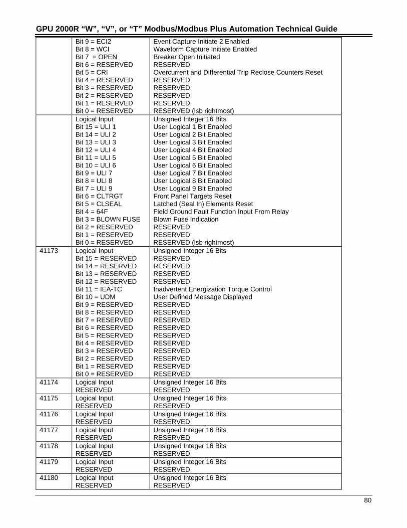
GPU 2000R “W”, “V”, or “T” Modbus/Modbus Plus Automation Technical Guide
80
Bit 9 = ECI2Bit 8 = WCIBit 7 = OPENBit 6 = RESERVEDBit 5 = CRIBit 4 = RESERVEDBit 3 = RESERVEDBit 2 = RESERVEDBit 1 = RESERVEDBit 0 = RESERVED
Event Capture Initiate 2 EnabledWaveform Capture Initiate EnabledBreaker Open InitiatedRESERVEDOvercurrent and Differential Trip Reclose Counters ResetRESERVEDRESERVEDRESERVEDRESERVEDRESERVED (lsb rightmost)
Logical InputBit 15 = ULI 1Bit 14 = ULI 2Bit 13 = ULI 3Bit 12 = ULI 4Bit 11 = ULI 5Bit 10 = ULI 6Bit 9 = ULI 7Bit 8 = ULI 8Bit 7 = ULI 9Bit 6 = CLTRGTBit 5 = CLSEALBit 4 = 64FBit 3 = BLOWN FUSEBit 2 = RESERVEDBit 1 = RESERVEDBit 0 = RESERVED
Unsigned Integer 16 BitsUser Logical 1 Bit EnabledUser Logical 2 Bit EnabledUser Logical 3 Bit EnabledUser Logical 4 Bit EnabledUser Logical 5 Bit EnabledUser Logical 6 Bit EnabledUser Logical 7 Bit EnabledUser Logical 8 Bit EnabledUser Logical 9 Bit EnabledFront Panel Targets ResetLatched (Seal In) Elements ResetField Ground Fault Function Input From RelayBlown Fuse IndicationRESERVEDRESERVEDRESERVED (lsb rightmost)
41173 Logical InputBit 15 = RESERVEDBit 14 = RESERVEDBit 13 = RESERVEDBit 12 = RESERVEDBit 11 = IEA-TCBit 10 = UDMBit 9 = RESERVEDBit 8 = RESERVEDBit 7 = RESERVEDBit 6 = RESERVEDBit 5 = RESERVEDBit 4 = RESERVEDBit 3 = RESERVEDBit 2 = RESERVEDBit 1 = RESERVEDBit 0 = RESERVED
Unsigned Integer 16 BitsRESERVEDRESERVEDRESERVEDRESERVEDInadvertent Energization Torque ControlUser Defined Message DisplayedRESERVEDRESERVEDRESERVEDRESERVEDRESERVEDRESERVEDRESERVEDRESERVEDRESERVEDRESERVED
41174 Logical InputRESERVED
Unsigned Integer 16 BitsRESERVED
41175 Logical InputRESERVED
Unsigned Integer 16 BitsRESERVED
41176 Logical InputRESERVED
Unsigned Integer 16 BitsRESERVED
41177 Logical InputRESERVED
Unsigned Integer 16 BitsRESERVED
41178 Logical InputRESERVED
Unsigned Integer 16 BitsRESERVED
41179 Logical InputRESERVED
Unsigned Integer 16 BitsRESERVED
41180 Logical InputRESERVED
Unsigned Integer 16 BitsRESERVED
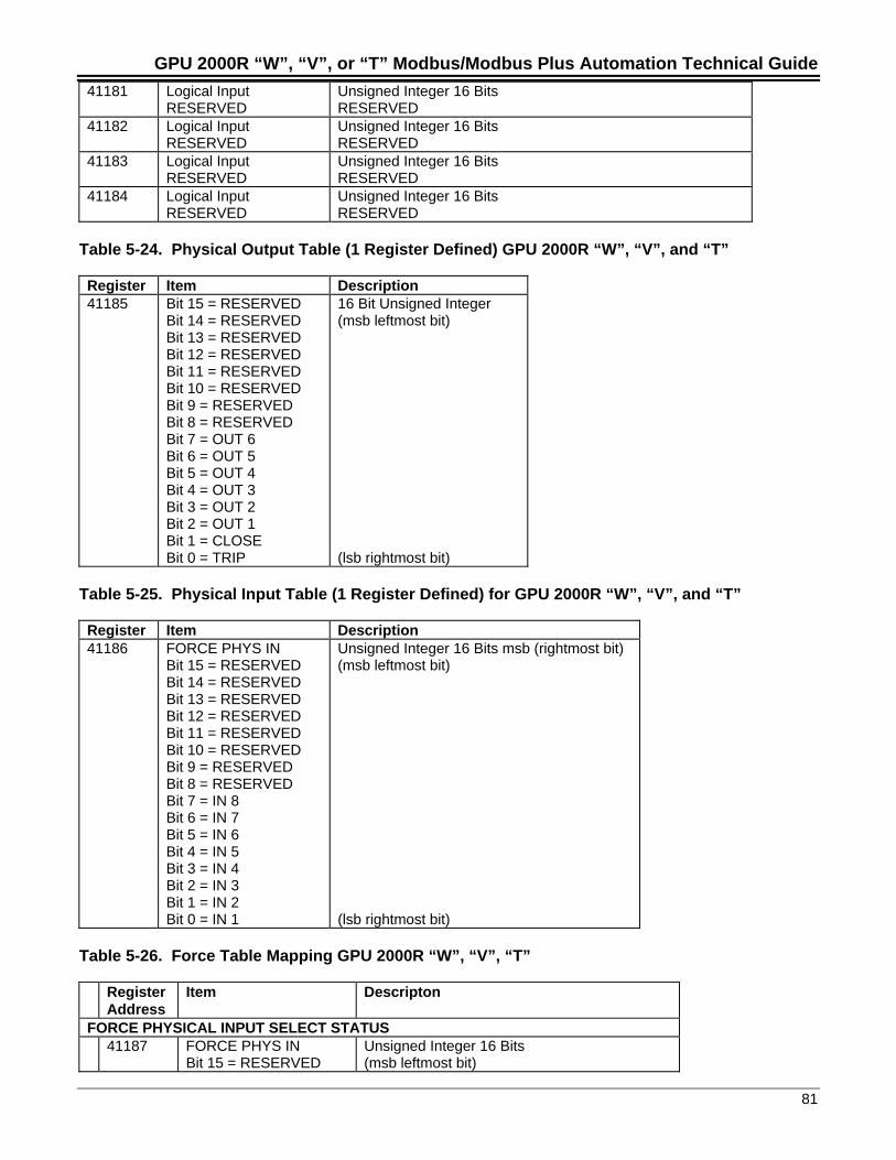
GPU 2000R “W”, “V”, or “T” Modbus/Modbus Plus Automation Technical Guide
81
41181 Logical InputRESERVED
Unsigned Integer 16 BitsRESERVED
41182 Logical InputRESERVED
Unsigned Integer 16 BitsRESERVED
41183 Logical InputRESERVED
Unsigned Integer 16 BitsRESERVED
41184 Logical InputRESERVED
Unsigned Integer 16 BitsRESERVED
Table 5-24. Physical Output Table (1 Register Defined) GPU 2000R “W”, “V”, and “T”
Register Item Description41185 Bit 15 = RESERVED
Bit 14 = RESERVEDBit 13 = RESERVEDBit 12 = RESERVEDBit 11 = RESERVEDBit 10 = RESERVEDBit 9 = RESERVEDBit 8 = RESERVEDBit 7 = OUT 6Bit 6 = OUT 5Bit 5 = OUT 4Bit 4 = OUT 3Bit 3 = OUT 2Bit 2 = OUT 1Bit 1 = CLOSEBit 0 = TRIP
16 Bit Unsigned Integer(msb leftmost bit)
(lsb rightmost bit)
Table 5-25. Physical Input Table (1 Register Defined) for GPU 2000R “W”, “V”, and “T”
Register Item Description41186 FORCE PHYS IN
Bit 15 = RESERVEDBit 14 = RESERVEDBit 13 = RESERVEDBit 12 = RESERVEDBit 11 = RESERVEDBit 10 = RESERVEDBit 9 = RESERVEDBit 8 = RESERVEDBit 7 = IN 8Bit 6 = IN 7Bit 5 = IN 6Bit 4 = IN 5Bit 3 = IN 4Bit 2 = IN 3Bit 1 = IN 2Bit 0 = IN 1
Unsigned Integer 16 Bits msb (rightmost bit)(msb leftmost bit)
(lsb rightmost bit)
Table 5-26. Force Table Mapping GPU 2000R “W”, “V”, “T”
RegisterAddress
Item Descripton
FORCE PHYSICAL INPUT SELECT STATUS41187 FORCE PHYS IN
Bit 15 = RESERVEDUnsigned Integer 16 Bits(msb leftmost bit)
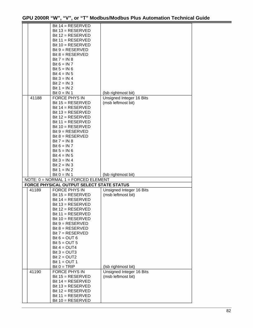
GPU 2000R “W”, “V”, or “T” Modbus/Modbus Plus Automation Technical Guide
82
Bit 14 = RESERVEDBit 13 = RESERVEDBit 12 = RESERVEDBit 11 = RESERVEDBit 10 = RESERVEDBit 9 = RESERVEDBit 8 = RESERVEDBit 7 = IN 8Bit 6 = IN 7Bit 5 = IN 6Bit 4 = IN 5Bit 3 = IN 4Bit 2 = IN 3Bit 1 = IN 2Bit 0 = IN 1 (lsb rightmost bit)
41188 FORCE PHYS INBit 15 = RESERVEDBit 14 = RESERVEDBit 13 = RESERVEDBit 12 = RESERVEDBit 11 = RESERVEDBit 10 = RESERVEDBit 9 = RESERVEDBit 8 = RESERVEDBit 7 = IN 8Bit 6 = IN 7Bit 5 = IN 6Bit 4 = IN 5Bit 3 = IN 4Bit 2 = IN 3Bit 1 = IN 2Bit 0 = IN 1
Unsigned Integer 16 Bits(msb leftmost bit)
(lsb rightmost bit)NOTE: 0 = NORMAL 1 = FORCED ELEMENTFORCE PHYSICAL OUTPUT SELECT STATE STATUS
41189 FORCE PHYS INBit 15 = RESERVEDBit 14 = RESERVEDBit 13 = RESERVEDBit 12 = RESERVEDBit 11 = RESERVEDBit 10 = RESERVEDBit 9 = RESERVEDBit 8 = RESERVEDBit 7 = RESERVEDBit 6 = OUT 6Bit 5 = OUT 5Bit 4 = OUT4Bit 3 = OUT3Bit 2 = OUT2Bit 1 = OUT 1Bit 0 = TRIP
Unsigned Integer 16 Bits(msb leftmost bit)
(lsb rightmost bit)41190 FORCE PHYS IN
Bit 15 = RESERVEDBit 14 = RESERVEDBit 13 = RESERVEDBit 12 = RESERVEDBit 11 = RESERVEDBit 10 = RESERVED
Unsigned Integer 16 Bits(msb leftmost bit)
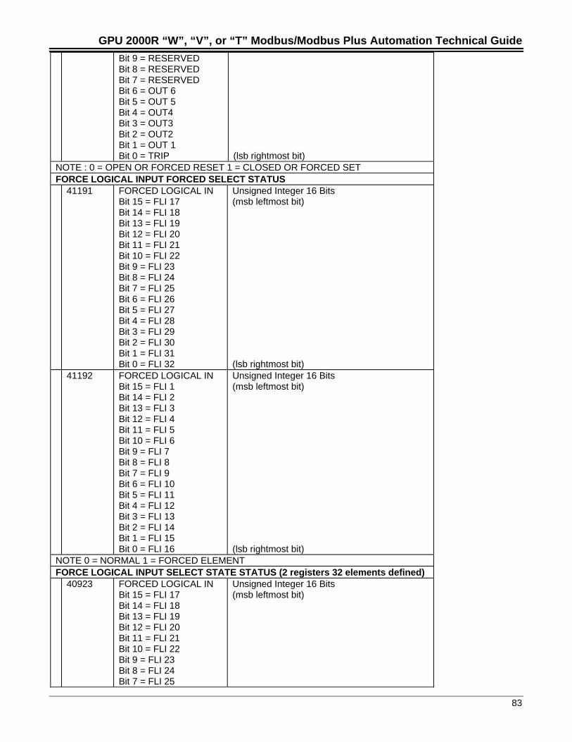
GPU 2000R “W”, “V”, or “T” Modbus/Modbus Plus Automation Technical Guide
83
Bit 9 = RESERVEDBit 8 = RESERVEDBit 7 = RESERVEDBit 6 = OUT 6Bit 5 = OUT 5Bit 4 = OUT4Bit 3 = OUT3Bit 2 = OUT2Bit 1 = OUT 1Bit 0 = TRIP (lsb rightmost bit)
NOTE : 0 = OPEN OR FORCED RESET 1 = CLOSED OR FORCED SETFORCE LOGICAL INPUT FORCED SELECT STATUS
41191 FORCED LOGICAL INBit 15 = FLI 17Bit 14 = FLI 18Bit 13 = FLI 19Bit 12 = FLI 20Bit 11 = FLI 21Bit 10 = FLI 22Bit 9 = FLI 23Bit 8 = FLI 24Bit 7 = FLI 25Bit 6 = FLI 26Bit 5 = FLI 27Bit 4 = FLI 28Bit 3 = FLI 29Bit 2 = FLI 30Bit 1 = FLI 31Bit 0 = FLI 32
Unsigned Integer 16 Bits(msb leftmost bit)
(lsb rightmost bit)41192 FORCED LOGICAL IN
Bit 15 = FLI 1Bit 14 = FLI 2Bit 13 = FLI 3Bit 12 = FLI 4Bit 11 = FLI 5Bit 10 = FLI 6Bit 9 = FLI 7Bit 8 = FLI 8Bit 7 = FLI 9Bit 6 = FLI 10Bit 5 = FLI 11Bit 4 = FLI 12Bit 3 = FLI 13Bit 2 = FLI 14Bit 1 = FLI 15Bit 0 = FLI 16
Unsigned Integer 16 Bits(msb leftmost bit)
(lsb rightmost bit)NOTE 0 = NORMAL 1 = FORCED ELEMENTFORCE LOGICAL INPUT SELECT STATE STATUS (2 registers 32 elements defined)
40923 FORCED LOGICAL INBit 15 = FLI 17Bit 14 = FLI 18Bit 13 = FLI 19Bit 12 = FLI 20Bit 11 = FLI 21Bit 10 = FLI 22Bit 9 = FLI 23Bit 8 = FLI 24Bit 7 = FLI 25
Unsigned Integer 16 Bits(msb leftmost bit)
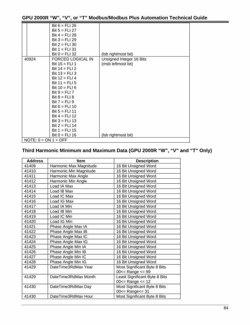
GPU 2000R “W”, “V”, or “T” Modbus/Modbus Plus Automation Technical Guide
84
Bit 6 = FLI 26Bit 5 = FLI 27Bit 4 = FLI 28Bit 3 = FLI 29Bit 2 = FLI 30Bit 1 = FLI 31Bit 0 = FLI 32 (lsb rightmost bit)
40924 FORCED LOGICAL INBit 15 = FLI 1Bit 14 = FLI 2Bit 13 = FLI 3Bit 12 = FLI 4Bit 11 = FLI 5Bit 10 = FLI 6Bit 9 = FLI 7Bit 8 = FLI 8Bit 7 = FLI 9Bit 6 = FLI 10Bit 5 = FLI 11Bit 4 = FLI 12Bit 3 = FLI 13Bit 2 = FLI 14Bit 1 = FLI 15Bit 0 = FLI 16
Unsigned Integer 16 Bits(msb leftmost bit)
(lsb rightmost bit)NOTE: 0 = ON 1 = OFF
Third Harmonic Minimum and Maximum Data (GPU 2000R “W”, “V” and “T” Only)
Address Item Description41409 Harmonic Max Magnitude 16 Bit Unsigned Word41410 Harmonic Min Magnitude 16 Bit Unsigned Word41411 Harmonic Max Angle 16 Bit Unsigned Word41412 Harmonic Min Angle 16 Bit Unsigned Word41413 Load IA Max 16 Bit Unsigned Word41414 Load IB Max 16 Bit Unsigned Word41415 Load IC Max 16 Bit Unsigned Word41416 Load IG Max 16 Bit Unsigned Word41417 Load IA Min 16 Bit Unsigned Word41418 Load IB Min 16 Bit Unsigned Word41419 Load IC Min 16 Bit Unsigned Word41420 Load IG Min 16 Bit Unsigned Word41421 Phase Angle Max IA 16 Bit Unsigned Word41422 Phase Angle Max IB 16 Bit Unsigned Word41423 Phase Angle Max IC 16 Bit Unsigned Word41424 Phase Angle Max IG 16 Bit Unsigned Word41425 Phase Angle Min IA 16 Bit Unsigned Word41426 Phase Angle Min IB 16 Bit Unsigned Word41427 Phase Angle Min IC 16 Bit Unsigned Word41428 Phase Angle Min IG 16 Bit Unsigned Word41429 DateTime3RdMax Year Most Significant Byte 8 Bits
00<= Range <= 9941429 DateTime3RdMax Month Least Significant Byte 8 Bits
00<= Range <= 1241430 DateTime3RdMax Day Most Significant Byte 8 Bits
00<= Range<= 3141430 DateTime3RdMax Hour Most Significant Byte 8 Bits
GPU 2000R “W”, “V”, or “T” Modbus/Modbus Plus Automation Technical Guide
85
00<= Range <= 2341431 DateTime3RdMax Minute Most Significant Byte 8 Bits
00<= Range <= 5941431 Reserved RESERVED41432 DateTime3RdMin Year Most Significant Byte 8 Bits
00<= Range <= 9941432 DateTime3RdMin Month Least Significant Byte 8 Bits
00<= Range <= 1241433 DateTime3RdMin Day Most Significant Byte 8 Bits
00<= Range<= 3141433 DateTime3RdMin Hour Most Significant Byte 8 Bits
00<= Range <= 2341434 Reserved RESERVED
Providing Control Functionality in the GPU 2000R
As described in the beginning of this section, six groups of control blocks are resident in the GPU 2000R. Eachgroup is comprised of 6 registers. The six control block groups are defined in Table 5-27. The first block withinthe set of registers determines whether or not the control block requires password control.
ABB relays are designed to operate with a variety of host products. Some host products cannot send a passwordwith the control algorithm. With this in mind, the ABB GPU 2000R “W”, “V”, or “T” version allows control, with orwithout password depending upon the setup performed in control register block 62560 through 62598. Within theGPU 2000R “W”, “T” or “V” version, a Security Mask Configuration Register 62598 contains a bit as to when thecorresponding bit is set, the control block associated with the bit disables password control. If the appropriate bitin Register 62598 is a value of “0”, then password protection is required to actuate control functionality. Pleaserefer to the 6X-register control section or GPU ECP screens for additional information regarding configuration ofthese registers.
One 4X register at the beginning of the 4X control register groups is “read only” which feeds back the status ofpassword control which was configured via Registers 62560 through 62598 (Security Mask Control Block, viaGPU 2000R “W”, “V”, or “T” only) or via the Communications Configuration Screen accessible through GPU ECP.The register lists the six control blocks found in the GPU 2000R Table 5-27 lists the Security Mask register, whichreports, which of the control blocks require password control. A status of 1 in the defined bit location allows anyvalue to be placed in the password field (as shown in Table 2). The Security mask status of what wasprogrammed through GPU ECP (“W”, “V”, or “T” versions only) or Modbus Registers 62560 through 62598 maybe obtained by reading Register 41537 (GPU 2000R “W”, “V”, or “T” only”). A status of 0 in the defined fieldrequires the correct password to be sent as part of the control process.
Figure 5-29 illustrates the Group Blocks within the GPU 2000R and its associated typical control registermapping. Note the ranges of block information for the differing models. 41537 though 41585 for the “W”, “V” and“T” units.
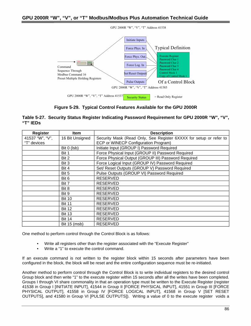
GPU 2000R “W”, “V”, or “T” Modbus/Modbus Plus Automation Technical Guide
86
Execute RegisterPassword Char 1Password Char 2Password Char 3Password Char 4Control Mask 1Copy of Control Mask 1
Initiate Inputs
Force Phys. In
Force Phys. Out.
Force Log. In
Set/Reset Outputs
Pulse Outputs
Typical Definition
EC
Of a Control Block
CommandSequence ThroughModbus Command 16Preset Multiple Holding Registers
Security Status = Read Only RegisterGPU 2000R “W”, “V”, “T” Address 41537
GPU 2000R “W”, “V”, “T” Address 41538
GPU 2000R “W”, “V”, “T” Address 41585
Figure 5-29. Typical Control Features Available for the GPU 2000R
Table 5-27. Security Status Register Indicating Password Requirement for GPU 2000R “W”, “V”,“T” IEDs
Register Item Description41537 “W”, “V”,“T” devices
16 Bit Unsigned Security Mask (Read Only, See Register 6XXXX for setup or refer toECP or WINECP Configuration Program)
Bit 0 (lsb) Initiate Input (GROUP I) Password RequiredBit 1 Force Physical Input (GROUP II) Password RequiredBit 2 Force Physical Output (GROUP III) Password RequiredBit 3 Force Logical Input (GROUP IV) Password RequiredBit 4 Set/ Reset Outputs (GROUP V) Password RequiredBit 5 Pulse Outputs (GROUP VI) Password RequiredBit 6 RESERVEDBit 7 RESERVEDBit 8 RESERVEDBit 9 RESERVEDBit 10 RESERVEDBit 11 RESERVEDBit 12 RESERVEDBit 13 RESERVEDBit 14 RESERVEDBit 15 (msb) RESERVED
One method to perform control through the Control Block is as follows:
• Write all registers other than the register associated with the “Execute Register”• Write a “1” to execute the control command.
If an execute command is not written to the register block within 15 seconds after parameters have beenconfigured in the block, the block will be reset and the entire configuration sequence must be re-initiated.
Another method to perform control through the Control Block is to write individual registers to the desired controlGroup block and then write “1” to the execute register within 15 seconds after all the writes have been completed.Groups I through VI share commonality in that an operation type must be written to the Execute Register (register41538 in Group I [INITIATE INPUT], 41544 in Group II [FORCE PHYSICAL INPUT], 41551 in Group III [FORCEPHYSICAL OUTPUT], 41558 in Group IV [FORCE LOGICAL INPUT], 41568 in Group V [SET RESETOUTPUTS], and 41580 in Group VI [PULSE OUTPUTS]). Writing a value of 0 to the execute register voids a
GPU 2000R “W”, “V”, or “T” Modbus/Modbus Plus Automation Technical Guide
87
control execution of the function. Writing a Value of 1 to the execute register allows the function to operate if theconsecutive registers are parameterized correctly.
A correct Password may have to be written to the block for the desired function to execute (Registers 41539 and41540 in Group I [INITIATE INPUT], 41545 and 41546 in Group II [FORCE PHYSICAL INPUT], 41552 and 41553in Group III [FORCE PHYSICAL OUTPUT], 41559 and 41560 in Group IV [FORCE LOGICAL INPUT], 41569 and41570 in Group V [SET RESET OUTPUTS] , and 41581 and 41582 in Group VI [PULSE OUTPUTS]) The GPU2000R contains a default password of four spaces. If Appendix B is consulted, the ASCII code for a space is 20(HEX). Thus the numerical value to be sent to the registers corresponding to the default password is 2020 (HEX)for password register 1 and 2020 (HEX) for password register 2.
IMPLEMENTATION TIP– If control does not occur after initiation through the network, verify that thelocal/remote control bit is not configured in the programmable logical inputs logic or that the local/remotecontrol bit is in the remote state. If the local/remote control bit is configured, and the control switch is inthe local position (indicating that control via the network is inhibited), if one of the control commands aresent via the network, a modbus exception response shall be sent to the host rejecting the command. Ifthe local/remote control bit is not configured, control may take place via the operator interface panel(MMI) or via the network contemporaneously. Additionally, Modbus Registers 40172 through 40175, ifRead using Modbus code “03” shall indicate the nature of the communication control errors of the lastcontrol function.
Group I Control Features Explained
Group I provides the following functionality:• Trip Initiate
Group I control requires that the control bit be selected in Register 41542 and the same corresponding valueshould also be placed in 41543. If the values in the registers do not match, control shall not occur.
Table 5-28. Group I Control Registers
Register Item DescriptionGROUP I41538 Execute Register
0 = No Action1 = Execute
Unsigned (16 Bits)
41539 Password ASCII – 2 Characters Leftmost Digits41540 Password ASCII – 2 Characters Rightmost Digits41541 Spare41542 Change Initiate Input Mask Unsigned (16 Bits)
Bit 0 Trip Initiate (lsb) 1 = Control Bit State 0 = No ControlBit 1 ReservedBit 2 ReservedBit 3 ReservedBit 4 ReservedBit 5 ReservedBit 6 ReservedBit 7 ReservedBit 8 ReservedBit 9 ReservedBit 10 ReservedBit 11 ReservedBit 12 ReservedBit 13 ReservedBit 14 ReservedBit 15 Reserved (msb)
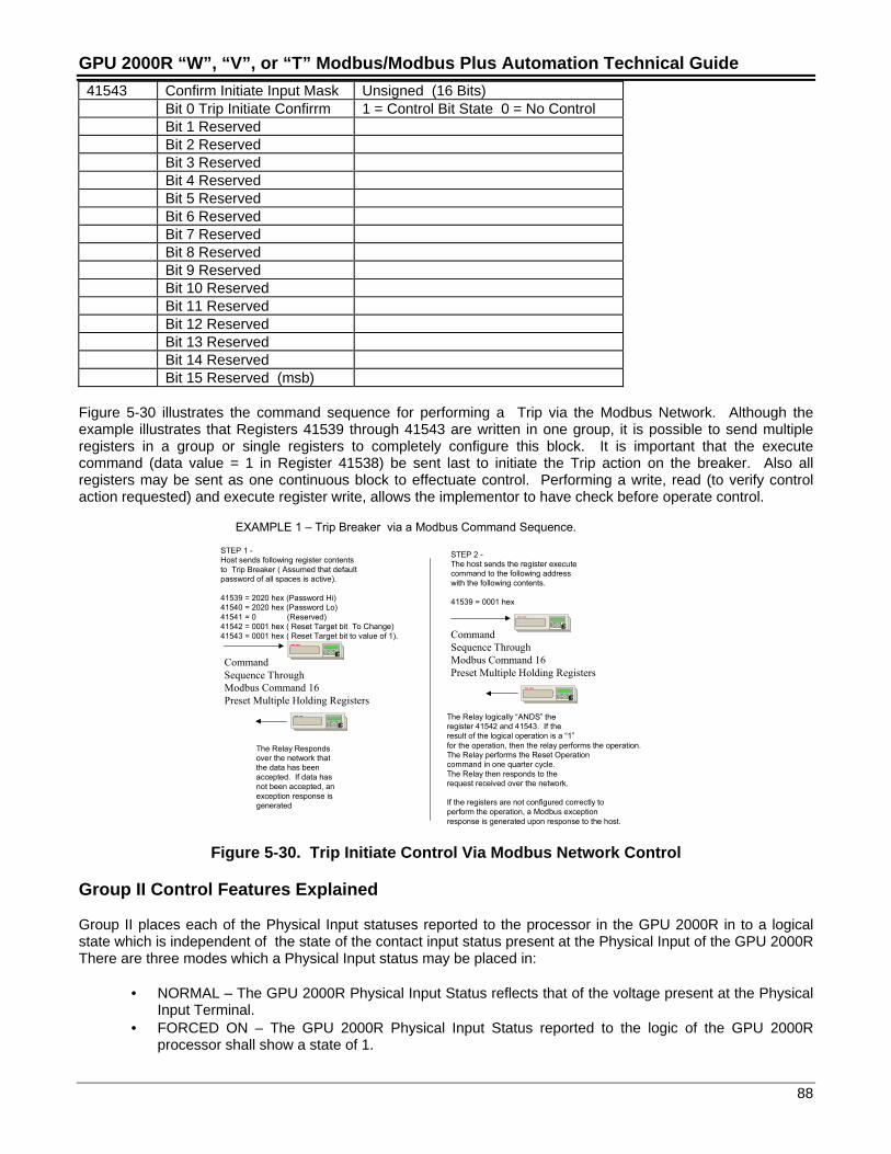
GPU 2000R “W”, “V”, or “T” Modbus/Modbus Plus Automation Technical Guide
88
41543 Confirm Initiate Input Mask Unsigned (16 Bits)Bit 0 Trip Initiate Confirrm 1 = Control Bit State 0 = No ControlBit 1 ReservedBit 2 ReservedBit 3 ReservedBit 4 ReservedBit 5 ReservedBit 6 ReservedBit 7 ReservedBit 8 ReservedBit 9 ReservedBit 10 ReservedBit 11 ReservedBit 12 ReservedBit 13 ReservedBit 14 ReservedBit 15 Reserved (msb)
Figure 5-30 illustrates the command sequence for performing a Trip via the Modbus Network. Although theexample illustrates that Registers 41539 through 41543 are written in one group, it is possible to send multipleregisters in a group or single registers to completely configure this block. It is important that the executecommand (data value = 1 in Register 41538) be sent last to initiate the Trip action on the breaker. Also allregisters may be sent as one continuous block to effectuate control. Performing a write, read (to verify controlaction requested) and execute register write, allows the implementor to have check before operate control.
ECCommandSequence ThroughModbus Command 16Preset Multiple Holding Registers
STEP 1 -Host sends following register contentsto Trip Breaker ( Assumed that defaultpassword of all spaces is active).
41539 = 2020 hex (Password Hi)41540 = 2020 hex (Password Lo)41541 = 0 (Reserved)41542 = 0001 hex ( Reset Target bit To Change)41543 = 0001 hex ( Reset Target bit to value of 1).
EXAMPLE 1 – Trip Breaker via a Modbus Command Sequence.
EC
The Relay logically “ANDS” the register 41542 and 41543. If the result of the logical operation is a “1”for the operation, then the relay performs the operation.The Relay performs the Reset Operationcommand in one quarter cycle.The Relay then responds to therequest received over the network.
If the registers are not configured correctly toperform the operation, a Modbus exception response is generated upon response to the host.
ECCommandSequence ThroughModbus Command 16Preset Multiple Holding Registers
STEP 2 -The host sends the register executecommand to the following address with the following contents.
41539 = 0001 hex
EC
The Relay Respondsover the network that the data has been accepted. If data has not been accepted, anexception response isgenerated
Figure 5-30. Trip Initiate Control Via Modbus Network Control
Group II Control Features Explained
Group II places each of the Physical Input statuses reported to the processor in the GPU 2000R in to a logicalstate which is independent of the state of the contact input status present at the Physical Input of the GPU 2000RThere are three modes which a Physical Input status may be placed in:
• NORMAL – The GPU 2000R Physical Input Status reflects that of the voltage present at the PhysicalInput Terminal.
• FORCED ON – The GPU 2000R Physical Input Status reported to the logic of the GPU 2000Rprocessor shall show a state of 1.
GPU 2000R “W”, “V”, or “T” Modbus/Modbus Plus Automation Technical Guide
89
• FORCED OFF – The GPU 2000R Physical Input Status reported to the logic of the GPU 2000Rprocessor shall show a state of 0.
The Force Physical Input State only affects the state reported to the central processor logic contained within theGPU 2000R. Table 5-29 lists the definition of the control registers and maps each of the internal control bits.Seven Registers are required to perform control for Group II functions. When the control is accepted, the GREENNORMAL LED at the front panel interface of the device will flash. The status of the force can also be confirmedvia GPU ECP.
Table 5-29. Group II Bit Definitions for GPU 2000R Control
Register Item DescriptionGROUP II41544 Execute Register
0 = No Action1 = Execute
Unsigned (16 Bits)
41545 Password ASCII – 2 Characters Leftmost Digits41546 Password ASCII – 2 Characters Rightmost Digits41547 Spare41548 Force Physical Input Change Mask Unsigned (16 Bits)
Bit 0 Input 1 (Terminal 4) (lsb) 1 = Control Bit State 0 = No Control (lsb)Bit 1 Input 2 (Terminal 5) 1 = Control Bit State 0 = No ControlBit 2 Input 3 (Terminal 6) 1 = Control Bit State 0 = No ControlBit 3 Input 4 (Terminal 7) 1 = Control Bit State 0 = No ControlBit 4 Input 5 (Terminal 8) 1 = Control Bit State 0 = No ControlBit 5 Input 6 (Terminal 9) 1 = Control Bit State 0 = No ControlBit 6 Input 7 (Terminal 10) 1 = Control Bit State 0 = No ControlBit 7 Input 8 (Terminal 12) 1 = Control Bit State 0 = No ControlBit 8 Input 9 (Terminal 12) 1 = Control Bit State 0 = No ControlBit 9 ReservedBit 10 ReservedBit 11 ReservedBit 12 ReservedBit 13 ReservedBit 14 ReservedBit 15 Reserved (msb)
41549 Force Physical Input Normal State Mask Unsigned (16 Bits)Bit 0 Input 1 (Terminal 4) (lsb) 1 = Normal State Override 0 = Normal StateBit 1 Input 2 (Terminal 5) 1 = Normal State Override 0 = Normal StateBit 2 Input 3 (Terminal 6) 1 = Normal State Override 0 = Normal StateBit 3 Input 4 (Terminal 7) 1 = Normal State Override 0 = Normal StateBit 4 Input 5 (Terminal 8) 1 = Normal State Override 0 = Normal StateBit 5 Input 6 (Terminal 9) 1 = Normal State Override 0 = Normal StateBit 6 Input 7 (Terminal 10) 1 = Normal State Override 0 = Normal StateBit 7 Input 8 (Terminal 12) 1 = Normal State Override 0 = Normal StateBit 8 Input 9 (Terminal 12) 1 = Normal State Override 0 = Normal StateBit 9 ReservedBit 10 ReservedBit 11 ReservedBit 12 ReservedBit 13 ReservedBit 14 ReservedBit 15 Reserved (msb)
41550 Force Physical Input Forcing State Mask Unsigned (16 Bits)Bit 0 Input 1 (Terminal 4) (lsb) 1 = Force Set State 0 = Force Reset State
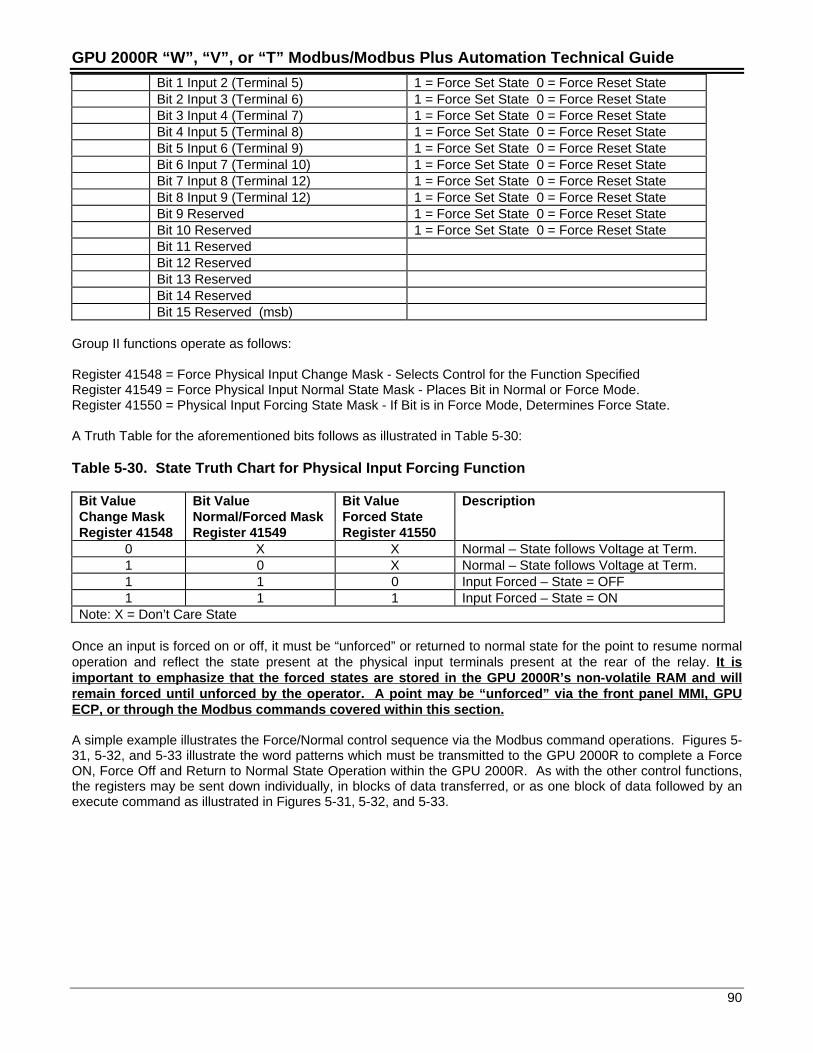
GPU 2000R “W”, “V”, or “T” Modbus/Modbus Plus Automation Technical Guide
90
Bit 1 Input 2 (Terminal 5) 1 = Force Set State 0 = Force Reset StateBit 2 Input 3 (Terminal 6) 1 = Force Set State 0 = Force Reset StateBit 3 Input 4 (Terminal 7) 1 = Force Set State 0 = Force Reset StateBit 4 Input 5 (Terminal 8) 1 = Force Set State 0 = Force Reset StateBit 5 Input 6 (Terminal 9) 1 = Force Set State 0 = Force Reset StateBit 6 Input 7 (Terminal 10) 1 = Force Set State 0 = Force Reset StateBit 7 Input 8 (Terminal 12) 1 = Force Set State 0 = Force Reset StateBit 8 Input 9 (Terminal 12) 1 = Force Set State 0 = Force Reset StateBit 9 Reserved 1 = Force Set State 0 = Force Reset StateBit 10 Reserved 1 = Force Set State 0 = Force Reset StateBit 11 ReservedBit 12 ReservedBit 13 ReservedBit 14 ReservedBit 15 Reserved (msb)
Group II functions operate as follows:
Register 41548 = Force Physical Input Change Mask - Selects Control for the Function SpecifiedRegister 41549 = Force Physical Input Normal State Mask - Places Bit in Normal or Force Mode.Register 41550 = Physical Input Forcing State Mask - If Bit is in Force Mode, Determines Force State.
A Truth Table for the aforementioned bits follows as illustrated in Table 5-30:
Table 5-30. State Truth Chart for Physical Input Forcing Function
Bit ValueChange MaskRegister 41548
Bit ValueNormal/Forced MaskRegister 41549
Bit ValueForced StateRegister 41550
Description
0 X X Normal – State follows Voltage at Term.1 0 X Normal – State follows Voltage at Term.1 1 0 Input Forced – State = OFF1 1 1 Input Forced – State = ON
Note: X = Don’t Care State
Once an input is forced on or off, it must be “unforced” or returned to normal state for the point to resume normaloperation and reflect the state present at the physical input terminals present at the rear of the relay. It isimportant to emphasize that the forced states are stored in the GPU 2000R’s non-volatile RAM and willremain forced until unforced by the operator. A point may be “unforced” via the front panel MMI, GPUECP, or through the Modbus commands covered within this section.
A simple example illustrates the Force/Normal control sequence via the Modbus command operations. Figures 5-31, 5-32, and 5-33 illustrate the word patterns which must be transmitted to the GPU 2000R to complete a ForceON, Force Off and Return to Normal State Operation within the GPU 2000R. As with the other control functions,the registers may be sent down individually, in blocks of data transferred, or as one block of data followed by anexecute command as illustrated in Figures 5-31, 5-32, and 5-33.
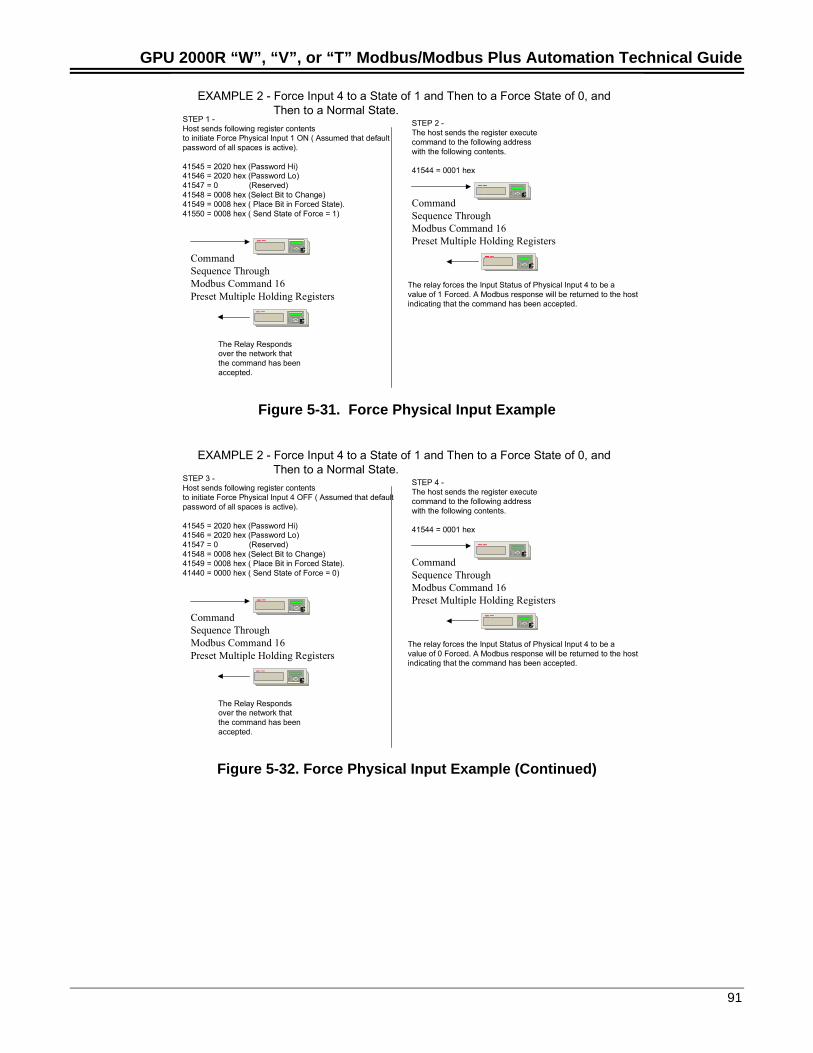
GPU 2000R “W”, “V”, or “T” Modbus/Modbus Plus Automation Technical Guide
91
ECCommandSequence ThroughModbus Command 16Preset Multiple Holding Registers
STEP 1 -Host sends following register contentsto initiate Force Physical Input 1 ON ( Assumed that defaultpassword of all spaces is active).
41545 = 2020 hex (Password Hi)41546 = 2020 hex (Password Lo)41547 = 0 (Reserved)41548 = 0008 hex (Select Bit to Change)41549 = 0008 hex ( Place Bit in Forced State).41550 = 0008 hex ( Send State of Force = 1)
EXAMPLE 2 - Force Input 4 to a State of 1 and Then to a Force State of 0, and Then to a Normal State.
EC
The relay forces the Input Status of Physical Input 4 to be a value of 1 Forced. A Modbus response will be returned to the hostindicating that the command has been accepted.
ECCommandSequence ThroughModbus Command 16Preset Multiple Holding Registers
STEP 2 -The host sends the register executecommand to the following address with the following contents.
41544 = 0001 hex
EC
The Relay Respondsover the network that the command has been accepted.
Figure 5-31. Force Physical Input Example
ECCommandSequence ThroughModbus Command 16Preset Multiple Holding Registers
STEP 3 -Host sends following register contentsto initiate Force Physical Input 4 OFF ( Assumed that defaultpassword of all spaces is active).
41545 = 2020 hex (Password Hi)41546 = 2020 hex (Password Lo)41547 = 0 (Reserved)41548 = 0008 hex (Select Bit to Change)41549 = 0008 hex ( Place Bit in Forced State).41440 = 0000 hex ( Send State of Force = 0)
EXAMPLE 2 - Force Input 4 to a State of 1 and Then to a Force State of 0, and Then to a Normal State.
EC
The relay forces the Input Status of Physical Input 4 to be a value of 0 Forced. A Modbus response will be returned to the hostindicating that the command has been accepted.
ECCommandSequence ThroughModbus Command 16Preset Multiple Holding Registers
STEP 4 -The host sends the register executecommand to the following address with the following contents.
41544 = 0001 hex
EC
The Relay Respondsover the network that the command has been accepted.
Figure 5-32. Force Physical Input Example (Continued)
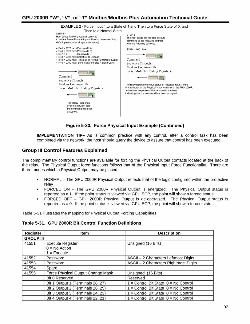
GPU 2000R “W”, “V”, or “T” Modbus/Modbus Plus Automation Technical Guide
92
ECCommandSequence ThroughModbus Command 16Preset Multiple Holding Registers
STEP 5 -Host sends following register contentsto initiate Force Physical Input 4 Normal ( Assumed that default password of all spaces is active).
41545 = 2020 hex (Password Hi)41546 = 2020 hex (Password Lo)41547 = 0 (Reserved)41548 = 0008 hex (Select Bit to Change)41549 = 0000 hex ( Place Bit in Normal “Unforced” State).41440 = 0000 hex ( Send State of Force = Don’t Care)
EXAMPLE 2 - Force Input 4 to a State of 1 and Then to a Force State of 0, and Then to a Normal State.
EC
The relay reports the Input Status of Physical Input 1 to be that reflected at the Physical Input terminals of the TPU 2000R.A Modbus response will be returned to the host
indicating that the command has been accepted.
ECCommandSequence ThroughModbus Command 16Preset Multiple Holding Registers
STEP 6 -The host sends the register executecommand to the following address with the following contents.
41544 = 0001 hex
EC
The Relay Respondsover the network that the command has been accepted.
Figure 5-33. Force Physical Input Example (Continued)
IMPLEMENTATION TIP– As is common practice with any control, after a control task has beencompleted via the network, the host should query the device to assure that control has been executed.
Group III Control Features Explained
The complimentary control functions are available for forcing the Physical Output contacts located at the back ofthe relay. The Physical Output force functions follows that of the Physical Input Force Functionality. There arethree modes which a Physical Output may be placed:
• NORMAL – The GPU 2000R Physical Output reflects that of the logic configured within the protectiverelay
• FORCED ON – The GPU 2000R Physical Output is energized. The Physical Output status isreported as a 1. If the point status is viewed via GPU ECP, the point will show a forced status
• FORCED OFF – GPU 2000R Physical Output is de-energized. The Physical Output status isreported as a 0. If the point status is viewed via GPU ECP, the point will show a forced status.
Table 5-31 illustrates the mapping for Physical Output Forcing Capabilities
Table 5-31. GPU 2000R Bit Control Function Definitions
Register Item DescriptionGROUP III41551 Execute Register
0 = No Action1 = Execute
Unsigned (16 Bits)
41552 Password ASCII – 2 Characters Leftmost Digits41553 Password ASCII – 2 Characters Rightmost Digits41554 Spare41555 Force Physical Output Change Mask Unsigned (16 Bits)
Bit 0 Reserved ReservedBit 1 Output 1 (Terminals 28, 27) 1 = Control Bit State 0 = No ControlBit 2 Output 2 (Terminals 26, 25) 1 = Control Bit State 0 = No ControlBit 3 Output 3 (Terminals 24, 23) 1 = Control Bit State 0 = No ControlBit 4 Output 4 (Terminals 22, 21) 1 = Control Bit State 0 = No Control
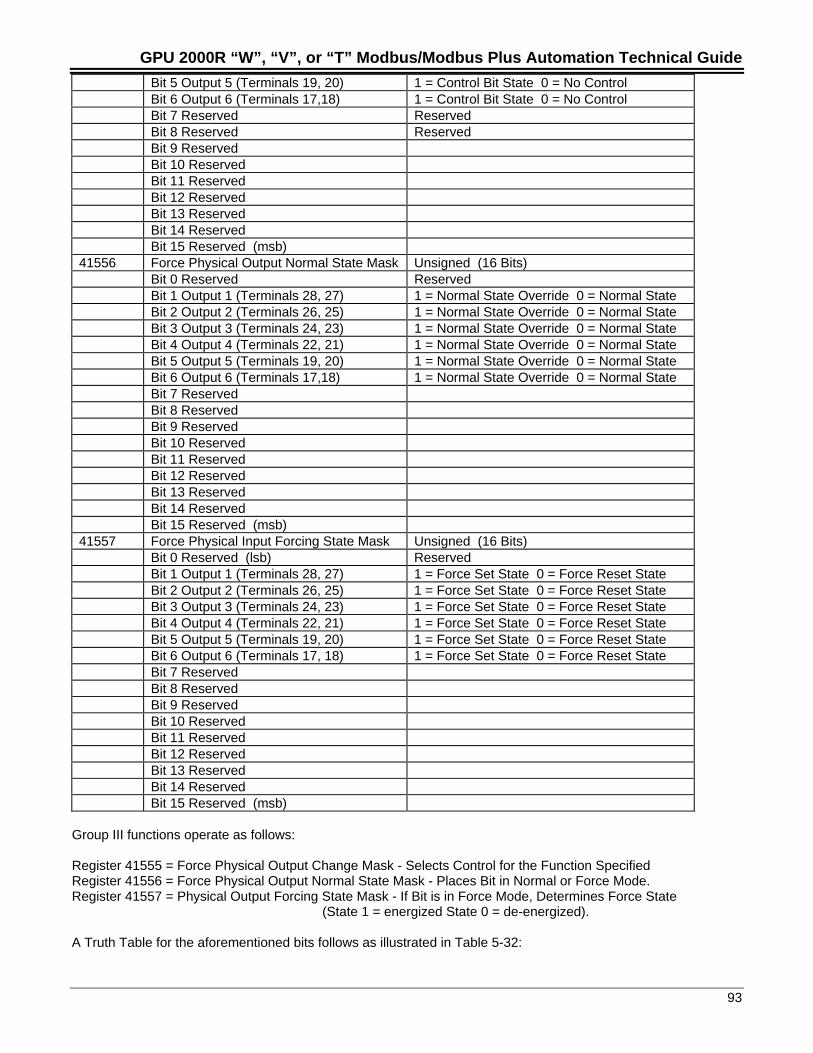
GPU 2000R “W”, “V”, or “T” Modbus/Modbus Plus Automation Technical Guide
93
Bit 5 Output 5 (Terminals 19, 20) 1 = Control Bit State 0 = No ControlBit 6 Output 6 (Terminals 17,18) 1 = Control Bit State 0 = No ControlBit 7 Reserved ReservedBit 8 Reserved ReservedBit 9 ReservedBit 10 ReservedBit 11 ReservedBit 12 ReservedBit 13 ReservedBit 14 ReservedBit 15 Reserved (msb)
41556 Force Physical Output Normal State Mask Unsigned (16 Bits)Bit 0 Reserved ReservedBit 1 Output 1 (Terminals 28, 27) 1 = Normal State Override 0 = Normal StateBit 2 Output 2 (Terminals 26, 25) 1 = Normal State Override 0 = Normal StateBit 3 Output 3 (Terminals 24, 23) 1 = Normal State Override 0 = Normal StateBit 4 Output 4 (Terminals 22, 21) 1 = Normal State Override 0 = Normal StateBit 5 Output 5 (Terminals 19, 20) 1 = Normal State Override 0 = Normal StateBit 6 Output 6 (Terminals 17,18) 1 = Normal State Override 0 = Normal StateBit 7 ReservedBit 8 ReservedBit 9 ReservedBit 10 ReservedBit 11 ReservedBit 12 ReservedBit 13 ReservedBit 14 ReservedBit 15 Reserved (msb)
41557 Force Physical Input Forcing State Mask Unsigned (16 Bits)Bit 0 Reserved (lsb) ReservedBit 1 Output 1 (Terminals 28, 27) 1 = Force Set State 0 = Force Reset StateBit 2 Output 2 (Terminals 26, 25) 1 = Force Set State 0 = Force Reset StateBit 3 Output 3 (Terminals 24, 23) 1 = Force Set State 0 = Force Reset StateBit 4 Output 4 (Terminals 22, 21) 1 = Force Set State 0 = Force Reset StateBit 5 Output 5 (Terminals 19, 20) 1 = Force Set State 0 = Force Reset StateBit 6 Output 6 (Terminals 17, 18) 1 = Force Set State 0 = Force Reset StateBit 7 ReservedBit 8 ReservedBit 9 ReservedBit 10 ReservedBit 11 ReservedBit 12 ReservedBit 13 ReservedBit 14 ReservedBit 15 Reserved (msb)
Group III functions operate as follows:
Register 41555 = Force Physical Output Change Mask - Selects Control for the Function SpecifiedRegister 41556 = Force Physical Output Normal State Mask - Places Bit in Normal or Force Mode.Register 41557 = Physical Output Forcing State Mask - If Bit is in Force Mode, Determines Force State
(State 1 = energized State 0 = de-energized).
A Truth Table for the aforementioned bits follows as illustrated in Table 5-32:
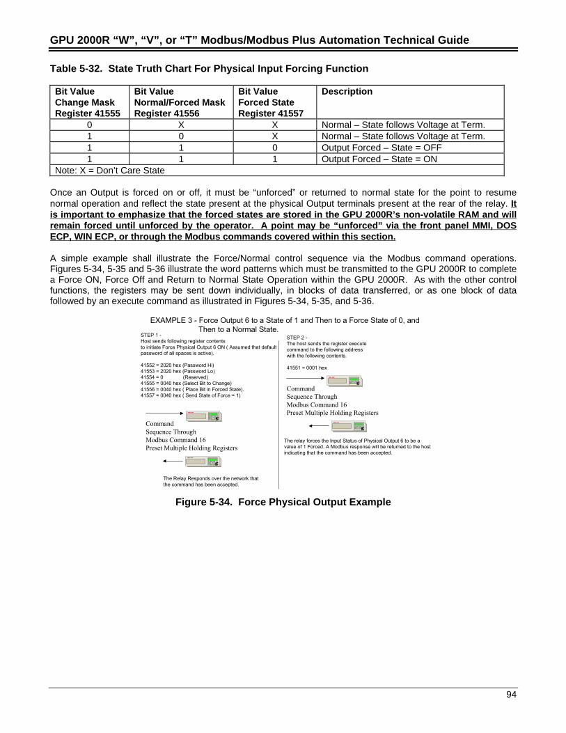
GPU 2000R “W”, “V”, or “T” Modbus/Modbus Plus Automation Technical Guide
94
Table 5-32. State Truth Chart For Physical Input Forcing Function
Bit ValueChange MaskRegister 41555
Bit ValueNormal/Forced MaskRegister 41556
Bit ValueForced StateRegister 41557
Description
0 X X Normal – State follows Voltage at Term.1 0 X Normal – State follows Voltage at Term.1 1 0 Output Forced – State = OFF1 1 1 Output Forced – State = ON
Note: X = Don’t Care State
Once an Output is forced on or off, it must be “unforced” or returned to normal state for the point to resumenormal operation and reflect the state present at the physical Output terminals present at the rear of the relay. Itis important to emphasize that the forced states are stored in the GPU 2000R’s non-volatile RAM and willremain forced until unforced by the operator. A point may be “unforced” via the front panel MMI, DOSECP, WIN ECP, or through the Modbus commands covered within this section.
A simple example shall illustrate the Force/Normal control sequence via the Modbus command operations.Figures 5-34, 5-35 and 5-36 illustrate the word patterns which must be transmitted to the GPU 2000R to completea Force ON, Force Off and Return to Normal State Operation within the GPU 2000R. As with the other controlfunctions, the registers may be sent down individually, in blocks of data transferred, or as one block of datafollowed by an execute command as illustrated in Figures 5-34, 5-35, and 5-36.
ECCommandSequence ThroughModbus Command 16Preset Multiple Holding Registers
STEP 1 -Host sends following register contentsto initiate Force Physical Output 6 ON ( Assumed that defaultpassword of all spaces is active).
41552 = 2020 hex (Password Hi)41553 = 2020 hex (Password Lo)41554 = 0 (Reserved)41555 = 0040 hex (Select Bit to Change)41556 = 0040 hex ( Place Bit in Forced State).41557 = 0040 hex ( Send State of Force = 1)
EXAMPLE 3 - Force Output 6 to a State of 1 and Then to a Force State of 0, and Then to a Normal State.
EC
The relay forces the Input Status of Physical Output 6 to be a value of 1 Forced. A Modbus response will be returned to the hostindicating that the command has been accepted.
ECCommandSequence ThroughModbus Command 16Preset Multiple Holding Registers
STEP 2 -The host sends the register executecommand to the following address with the following contents.
41551 = 0001 hex
EC
The Relay Responds over the network that the command has been accepted.
Figure 5-34. Force Physical Output Example
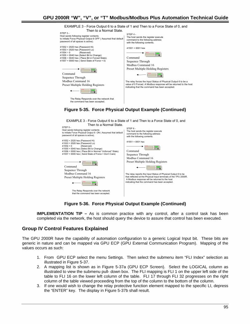
GPU 2000R “W”, “V”, or “T” Modbus/Modbus Plus Automation Technical Guide
95
ECCommandSequence ThroughModbus Command 16Preset Multiple Holding Registers
STEP 3 -Host sends following register contentsto initiate Force Physical Output 6 OFF ( Assumed that defaultpassword of all spaces is active).
41552 = 2020 hex (Password Hi)41553 = 2020 hex (Password Lo)41554 = 0 (Reserved)41555 = 0040 hex (Select Bit to Change)41556 = 0040 hex ( Place Bit in Forced State).41557 = 0000 hex ( Send State of Force = 0)
EXAMPLE 3 - Force Output 6 to a State of 1 and Then to a Force State of 0, and Then to a Normal State.
EC
The relay forces the Input Status of Physical Output 6 to be a value of 0 Forced. A Modbus response will be returned to the hostindicating that the command has been accepted.
ECCommandSequence ThroughModbus Command 16Preset Multiple Holding Registers
STEP 4 -The host sends the register executecommand to the following address with the following contents.
41551 = 0001 hex
EC
The Relay Responds over the network that the command has been accepted.
Figure 5-35. Force Physical Output Example (Continued)
ECCommandSequence ThroughModbus Command 16Preset Multiple Holding Registers
STEP 5 -Host sends following register contentsto initiate Force Physical Output 8 ON ( Assumed that defaultpassword of all spaces is active).
41552 = 2020 hex (Password Hi)41553 = 2020 hex (Password Lo)41554 = 0 (Reserved)41555 = 0040 hex (Select Bit to Change)41556 = 0000 hex ( Place Bit in Normal “Unforced” State).41557 = 0000 hex ( Send State of Force = Don’t Care)
EXAMPLE 3 - Force Output 6 to a State of 1 and Then to a Force State of 0, and Then to a Normal State.
EC
The relay reports the Input Status of Physical Output 6 to be that reflected at the Physical Input terminals of the TPU 2000R. A Modbus response will be returned to the hostindicating that the command has been accepted.
ECCommandSequence ThroughModbus Command 16Preset Multiple Holding Registers
STEP 6 -The host sends the register executecommand to the following address with the following contents.
41551 = 0001 hex
EC
The Relay Responds over the networkthat the command has been accepted.
Figure 5-36. Force Physical Output Example (Continued)
IMPLEMENTATION TIP – As is common practice with any control, after a control task has beencompleted via the network, the host should query the device to assure that control has been executed.
Group IV Control Features Explained
The GPU 2000R have the capability of automation configuration to a generic Logical Input bit. These bits aregeneric in nature and can be mapped via GPU ECP (GPU External Communication Program). Mapping of thevalues occurs as such:
1. From GPU ECP select the menu Settings. Then select the submenu item “FLI Index” selection asillustrated in Figure 5-37.
2. A mapping list is shown as in Figure 5-37a (GPU ECP Screen). Select the LOGICAL column asillustrated to view the submenu pull- down box. The FLI mapping is FLI 1 on the upper left side of thetable to FLI 16 on the lower left column of the table. FLI 17 through FLI 32 progresses on the rightcolumn of the table viewed proceeding from the top of the column to the bottom of the column.
3. If one would wish to change the relay protective function element mapped to the specific LI, depressthe “ENTER” key. The display in Figure 5-37b shall result.
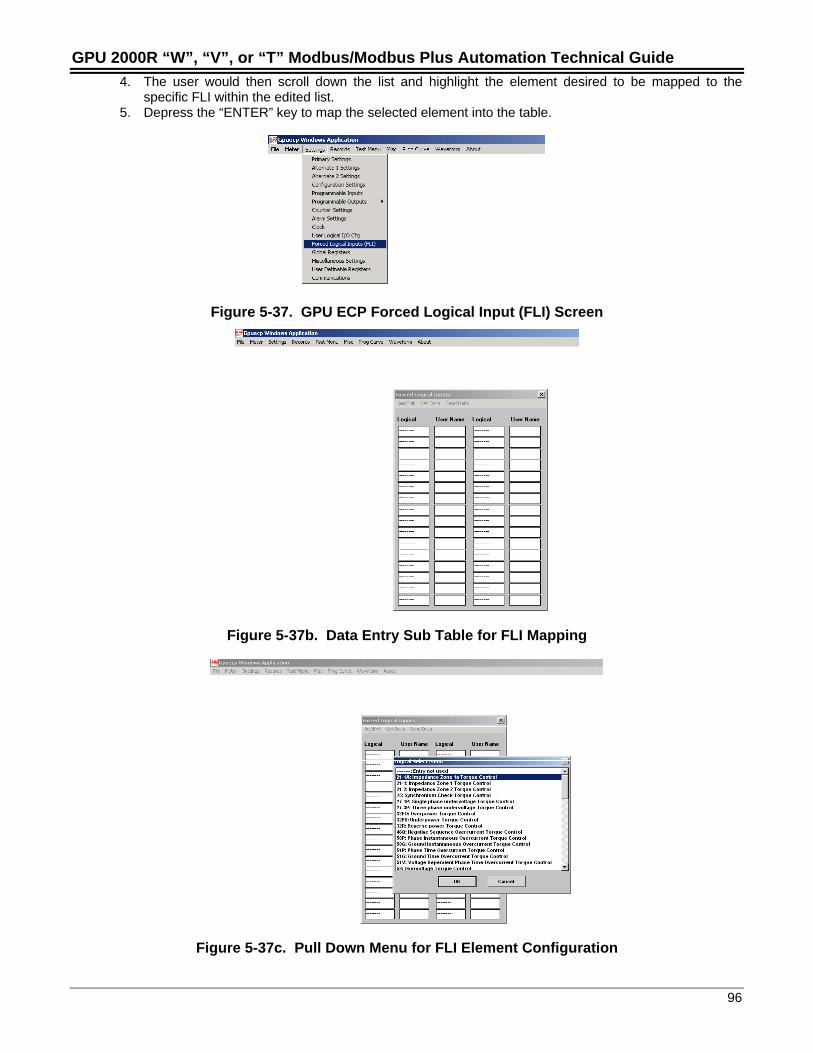
GPU 2000R “W”, “V”, or “T” Modbus/Modbus Plus Automation Technical Guide
96
4. The user would then scroll down the list and highlight the element desired to be mapped to thespecific FLI within the edited list.
5. Depress the “ENTER” key to map the selected element into the table.
Figure 5-37. GPU ECP Forced Logical Input (FLI) Screen
Figure 5-37b. Data Entry Sub Table for FLI Mapping
Figure 5-37c. Pull Down Menu for FLI Element Configuration
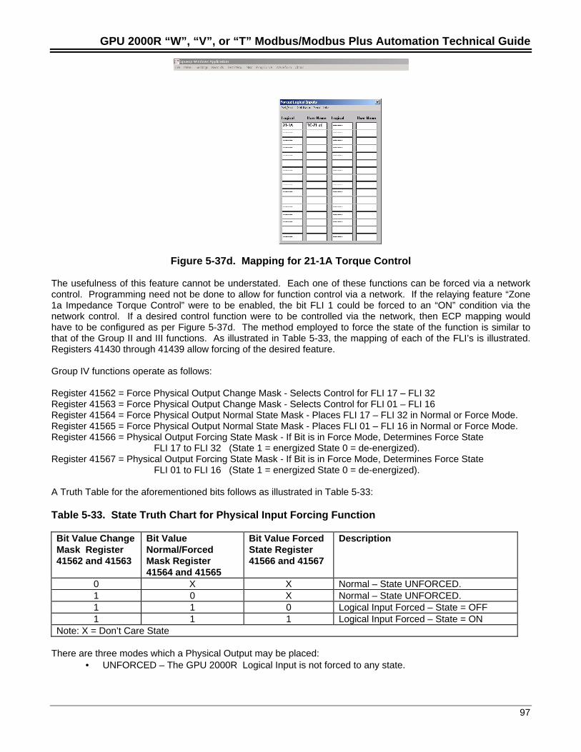
GPU 2000R “W”, “V”, or “T” Modbus/Modbus Plus Automation Technical Guide
97
Figure 5-37d. Mapping for 21-1A Torque Control
The usefulness of this feature cannot be understated. Each one of these functions can be forced via a networkcontrol. Programming need not be done to allow for function control via a network. If the relaying feature “Zone1a Impedance Torque Control” were to be enabled, the bit FLI 1 could be forced to an “ON” condition via thenetwork control. If a desired control function were to be controlled via the network, then ECP mapping wouldhave to be configured as per Figure 5-37d. The method employed to force the state of the function is similar tothat of the Group II and III functions. As illustrated in Table 5-33, the mapping of each of the FLI’s is illustrated.Registers 41430 through 41439 allow forcing of the desired feature.
Group IV functions operate as follows:
Register 41562 = Force Physical Output Change Mask - Selects Control for FLI 17 – FLI 32Register 41563 = Force Physical Output Change Mask - Selects Control for FLI 01 – FLI 16Register 41564 = Force Physical Output Normal State Mask - Places FLI 17 – FLI 32 in Normal or Force Mode.Register 41565 = Force Physical Output Normal State Mask - Places FLI 01 – FLI 16 in Normal or Force Mode.Register 41566 = Physical Output Forcing State Mask - If Bit is in Force Mode, Determines Force State
FLI 17 to FLI 32 (State 1 = energized State 0 = de-energized).Register 41567 = Physical Output Forcing State Mask - If Bit is in Force Mode, Determines Force State
FLI 01 to FLI 16 (State 1 = energized State 0 = de-energized).
A Truth Table for the aforementioned bits follows as illustrated in Table 5-33:
Table 5-33. State Truth Chart for Physical Input Forcing Function
Bit Value ChangeMask Register41562 and 41563
Bit ValueNormal/ForcedMask Register41564 and 41565
Bit Value ForcedState Register41566 and 41567
Description
0 X X Normal – State UNFORCED.1 0 X Normal – State UNFORCED.1 1 0 Logical Input Forced – State = OFF1 1 1 Logical Input Forced – State = ON
Note: X = Don’t Care State
There are three modes which a Physical Output may be placed:• UNFORCED – The GPU 2000R Logical Input is not forced to any state.
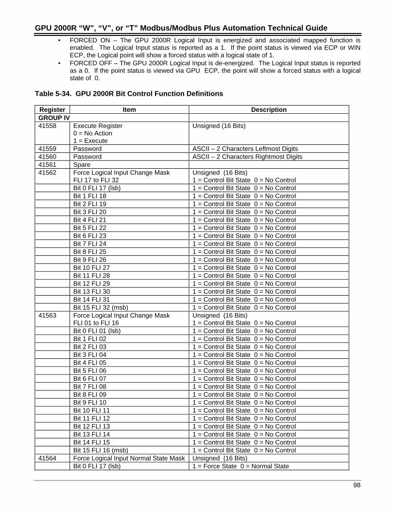
GPU 2000R “W”, “V”, or “T” Modbus/Modbus Plus Automation Technical Guide
98
• FORCED ON – The GPU 2000R Logical Input is energized and associated mapped function isenabled. The Logical Input status is reported as a 1. If the point status is viewed via ECP or WINECP, the Logical point will show a forced status with a logical state of 1.
• FORCED OFF – The GPU 2000R Logical Input is de-energized. The Logical Input status is reportedas a 0. If the point status is viewed via GPU ECP, the point will show a forced status with a logicalstate of 0.
Table 5-34. GPU 2000R Bit Control Function Definitions
Register Item DescriptionGROUP IV41558 Execute Register
0 = No Action1 = Execute
Unsigned (16 Bits)
41559 Password ASCII – 2 Characters Leftmost Digits41560 Password ASCII – 2 Characters Rightmost Digits41561 Spare41562 Force Logical Input Change Mask
FLI 17 to FLI 32Unsigned (16 Bits)1 = Control Bit State 0 = No Control
Bit 0 FLI 17 (lsb) 1 = Control Bit State 0 = No ControlBit 1 FLI 18 1 = Control Bit State 0 = No ControlBit 2 FLI 19 1 = Control Bit State 0 = No ControlBit 3 FLI 20 1 = Control Bit State 0 = No ControlBit 4 FLI 21 1 = Control Bit State 0 = No ControlBit 5 FLI 22 1 = Control Bit State 0 = No ControlBit 6 FLI 23 1 = Control Bit State 0 = No ControlBit 7 FLI 24 1 = Control Bit State 0 = No ControlBit 8 FLI 25 1 = Control Bit State 0 = No ControlBit 9 FLI 26 1 = Control Bit State 0 = No ControlBit 10 FLI 27 1 = Control Bit State 0 = No ControlBit 11 FLI 28 1 = Control Bit State 0 = No ControlBit 12 FLI 29 1 = Control Bit State 0 = No ControlBit 13 FLI 30 1 = Control Bit State 0 = No ControlBit 14 FLI 31 1 = Control Bit State 0 = No ControlBit 15 FLI 32 (msb) 1 = Control Bit State 0 = No Control
41563 Force Logical Input Change MaskFLI 01 to FLI 16
Unsigned (16 Bits)1 = Control Bit State 0 = No Control
Bit 0 FLI 01 (lsb) 1 = Control Bit State 0 = No ControlBit 1 FLI 02 1 = Control Bit State 0 = No ControlBit 2 FLI 03 1 = Control Bit State 0 = No ControlBit 3 FLI 04 1 = Control Bit State 0 = No ControlBit 4 FLI 05 1 = Control Bit State 0 = No ControlBit 5 FLI 06 1 = Control Bit State 0 = No ControlBit 6 FLI 07 1 = Control Bit State 0 = No ControlBit 7 FLI 08 1 = Control Bit State 0 = No ControlBit 8 FLI 09 1 = Control Bit State 0 = No ControlBit 9 FLI 10 1 = Control Bit State 0 = No ControlBit 10 FLI 11 1 = Control Bit State 0 = No ControlBit 11 FLI 12 1 = Control Bit State 0 = No ControlBit 12 FLI 13 1 = Control Bit State 0 = No ControlBit 13 FLI 14 1 = Control Bit State 0 = No ControlBit 14 FLI 15 1 = Control Bit State 0 = No ControlBit 15 FLI 16 (msb) 1 = Control Bit State 0 = No Control
41564 Force Logical Input Normal State Mask Unsigned (16 Bits)Bit 0 FLI 17 (lsb) 1 = Force State 0 = Normal State
GPU 2000R “W”, “V”, or “T” Modbus/Modbus Plus Automation Technical Guide
99
Bit 1 FLI 18 1 = Force State 0 = Normal StateBit 2 FLI 19 1 = Force State 0 = Normal StateBit 3 FLI 20 1 = Force State 0 = Normal StateBit 4 FLI 21 1 = Force State 0 = Normal StateBit 5 FLI 22 1 = Force State 0 = Normal StateBit 6 FLI 23 1 = Force State 0 = Normal StateBit 7 FLI 24 1 = Force State 0 = Normal StateBit 8 FLI 25 1 = Force State 0 = Normal StateBit 9 FLI 26 1 = Force State 0 = Normal StateBit 10 FLI 27 1 = Force State 0 = Normal StateBit 11 FLI 28 1 = Force State 0 = Normal StateBit 12 FLI 29 1 = Force State 0 = Normal StateBit 13 FLI 30 1 = Force State 0 = Normal StateBit 14 FLI 31 1 = Force State 0 = Normal StateBit 15 FLI 32 (msb) 1 = Force State 0 = Normal State
41565 Force Logical Input Normal State Mask Unsigned (16 Bits)Bit 0 FLI 01 (lsb) 1 = Force State 0 = Normal StateBit 1 FLI 02 1 = Force State 0 = Normal StateBit 2 FLI 03 1 = Force State 0 = Normal StateBit 3 FLI 04 1 = Force State 0 = Normal StateBit 4 FLI 05 1 = Force State 0 = Normal StateBit 5 FLI 06 1 = Force State 0 = Normal StateBit 6 FLI 07 1 = Force State 0 = Normal StateBit 7 FLI 08 1 = Force State 0 = Normal StateBit 8 FLI 09 1 = Force State 0 = Normal StateBit 9 FLI 10 1 = Force State 0 = Normal StateBit 10 FLI 11 1 = Force State 0 = Normal StateBit 11 FLI 12 1 = Force State 0 = Normal StateBit 12 FLI 13 1 = Force State 0 = Normal StateBit 13 FLI 14 1 = Force State 0 = Normal StateBit 14 FLI 15 1 = Force State 0 = Normal StateBit 15 FLI 16 (msb) 1 = Force State 0 = Normal State
41566 Force Logical Input State MaskFLI 17 – FLI 32
Unsigned (16 Bits)
Bit 0 FLI 17 (lsb) 1 = Force State 0 = Normal StateBit 1 FLI 18 1 = Force State 0 = Normal StateBit 2 FLI 19 1 = Force State 0 = Normal StateBit 3 FLI 20 1 = Force State 0 = Normal StateBit 4 FLI 21 1 = Force State 0 = Normal StateBit 5 FLI 22 1 = Force State 0 = Normal StateBit 6 FLI 23 1 = Force State 0 = Normal StateBit 7 FLI 24 1 = Force State 0 = Normal StateBit 8 FLI 25 1 = Force State 0 = Normal StateBit 9 FLI 26 1 = Force State 0 = Normal StateBit 10 FLI 27 1 = Force State 0 = Normal StateBit 11 FLI 28 1 = Force State 0 = Normal StateBit 12 FLI 29 1 = Force State 0 = Normal StateBit 13 FLI 30 1 = Force State 0 = Normal StateBit 14 FLI 31 1 = Force State 0 = Normal StateBit 15 FLI 32 (msb) 1 = Force State 0 = Normal State
41568 Force Logical Input State MaskFLI 01 – FLI 16
Unsigned (16 Bits)
Bit 0 FLI 01 (lsb) 1 = Force Set State 0 = Force Reset StateBit 1 FLI 02 1 = Force Set State 0 = Force Reset StateBit 2 FLI 03 1 = Force Set State 0 = Force Reset State
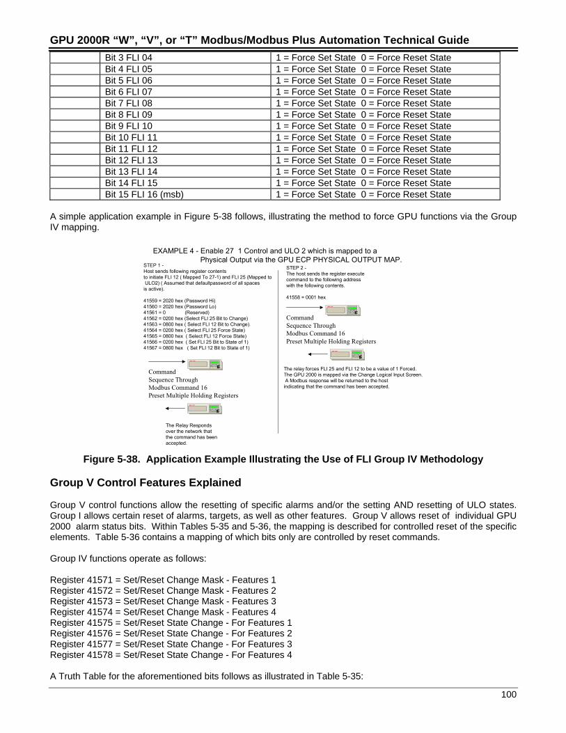
GPU 2000R “W”, “V”, or “T” Modbus/Modbus Plus Automation Technical Guide
100
Bit 3 FLI 04 1 = Force Set State 0 = Force Reset StateBit 4 FLI 05 1 = Force Set State 0 = Force Reset StateBit 5 FLI 06 1 = Force Set State 0 = Force Reset StateBit 6 FLI 07 1 = Force Set State 0 = Force Reset StateBit 7 FLI 08 1 = Force Set State 0 = Force Reset StateBit 8 FLI 09 1 = Force Set State 0 = Force Reset StateBit 9 FLI 10 1 = Force Set State 0 = Force Reset StateBit 10 FLI 11 1 = Force Set State 0 = Force Reset StateBit 11 FLI 12 1 = Force Set State 0 = Force Reset StateBit 12 FLI 13 1 = Force Set State 0 = Force Reset StateBit 13 FLI 14 1 = Force Set State 0 = Force Reset StateBit 14 FLI 15 1 = Force Set State 0 = Force Reset StateBit 15 FLI 16 (msb) 1 = Force Set State 0 = Force Reset State
A simple application example in Figure 5-38 follows, illustrating the method to force GPU functions via the GroupIV mapping.
ECCommandSequence ThroughModbus Command 16Preset Multiple Holding Registers
STEP 1 -Host sends following register contentsto initiate FLI 12 ( Mapped To 27-1) and FLI 25 (Mapped toULO2) ( Assumed that defaultpassword of all spaces
is active).
41559 = 2020 hex (Password Hi)41560 = 2020 hex (Password Lo)41561 = 0 (Reserved)41562 = 0200 hex (Select FLI 25 Bit to Change)41563 = 0800 hex ( Select FLI 12 Bit to Change).41564 = 0200 hex ( Select FLI 25 Force State)41565 = 0800 hex ( Select FLI 12 Force State)41566 = 0200 hex ( Set FLI 25 Bit to State of 1)41567 = 0800 hex ( Set FLI 12 Bit to State of 1)
EXAMPLE 4 - Enable 27 1 Control and ULO 2 which is mapped to a Physical Output via the GPU ECP PHYSICAL OUTPUT MAP.
EC
The relay forces FLI 25 and FLI 12 to be a value of 1 Forced.The GPU 2000 is mapped via the Change Logical Input Screen.A Modbus response will be returned to the hostindicating that the command has been accepted.
ECCommandSequence ThroughModbus Command 16Preset Multiple Holding Registers
STEP 2 -The host sends the register executecommand to the following address with the following contents.
41558 = 0001 hex
EC
The Relay Respondsover the network that the command has been accepted.
Figure 5-38. Application Example Illustrating the Use of FLI Group IV Methodology
Group V Control Features Explained
Group V control functions allow the resetting of specific alarms and/or the setting AND resetting of ULO states.Group I allows certain reset of alarms, targets, as well as other features. Group V allows reset of individual GPU2000 alarm status bits. Within Tables 5-35 and 5-36, the mapping is described for controlled reset of the specificelements. Table 5-36 contains a mapping of which bits only are controlled by reset commands.
Group IV functions operate as follows:
Register 41571 = Set/Reset Change Mask - Features 1Register 41572 = Set/Reset Change Mask - Features 2Register 41573 = Set/Reset Change Mask - Features 3Register 41574 = Set/Reset Change Mask - Features 4Register 41575 = Set/Reset State Change - For Features 1Register 41576 = Set/Reset State Change - For Features 2Register 41577 = Set/Reset State Change - For Features 3Register 41578 = Set/Reset State Change - For Features 4
A Truth Table for the aforementioned bits follows as illustrated in Table 5-35:
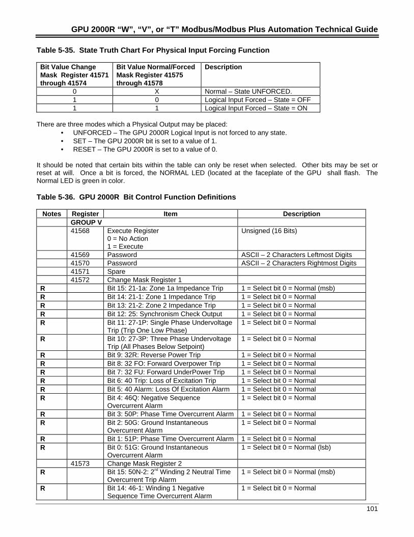
GPU 2000R “W”, “V”, or “T” Modbus/Modbus Plus Automation Technical Guide
101
Table 5-35. State Truth Chart For Physical Input Forcing Function
Bit Value ChangeMask Register 41571through 41574
Bit Value Normal/ForcedMask Register 41575through 41578
Description
0 X Normal – State UNFORCED.1 0 Logical Input Forced – State = OFF1 1 Logical Input Forced – State = ON
There are three modes which a Physical Output may be placed:• UNFORCED – The GPU 2000R Logical Input is not forced to any state.• SET – The GPU 2000R bit is set to a value of 1.• RESET – The GPU 2000R is set to a value of 0.
It should be noted that certain bits within the table can only be reset when selected. Other bits may be set orreset at will. Once a bit is forced, the NORMAL LED (located at the faceplate of the GPU shall flash. TheNormal LED is green in color.
Table 5-36. GPU 2000R Bit Control Function Definitions
Notes Register Item DescriptionGROUP V41568 Execute Register
0 = No Action1 = Execute
Unsigned (16 Bits)
41569 Password ASCII – 2 Characters Leftmost Digits41570 Password ASCII – 2 Characters Rightmost Digits41571 Spare41572 Change Mask Register 1
R Bit 15: 21-1a: Zone 1a Impedance Trip 1 = Select bit 0 = Normal (msb)R Bit 14: 21-1: Zone 1 Impedance Trip 1 = Select bit 0 = NormalR Bit 13: 21-2: Zone 2 Impedance Trip 1 = Select bit 0 = NormalR Bit 12: 25: Synchronism Check Output 1 = Select bit 0 = NormalR Bit 11: 27-1P: Single Phase Undervoltage
Trip (Trip One Low Phase)1 = Select bit 0 = Normal
R Bit 10: 27-3P: Three Phase UndervoltageTrip (All Phases Below Setpoint)
1 = Select bit 0 = Normal
R Bit 9: 32R: Reverse Power Trip 1 = Select bit 0 = NormalR Bit 8: 32 FO: Forward Overpower Trip 1 = Select bit 0 = NormalR Bit 7: 32 FU: Forward UnderPower Trip 1 = Select bit 0 = NormalR Bit 6: 40 Trip: Loss of Excitation Trip 1 = Select bit 0 = NormalR Bit 5: 40 Alarm: Loss Of Excitation Alarm 1 = Select bit 0 = NormalR Bit 4: 46Q: Negative Sequence
Overcurrent Alarm1 = Select bit 0 = Normal
R Bit 3: 50P: Phase Time Overcurrent Alarm 1 = Select bit 0 = NormalR Bit 2: 50G: Ground Instantaneous
Overcurrent Alarm1 = Select bit 0 = Normal
R Bit 1: 51P: Phase Time Overcurrent Alarm 1 = Select bit 0 = NormalR Bit 0: 51G: Ground Instantaneous
Overcurrent Alarm1 = Select bit 0 = Normal (lsb)
41573 Change Mask Register 2R Bit 15: 50N-2: 2nd Winding 2 Neutral Time
Overcurrent Trip Alarm1 = Select bit 0 = Normal (msb)
R Bit 14: 46-1: Winding 1 NegativeSequence Time Overcurrent Alarm
1 = Select bit 0 = Normal
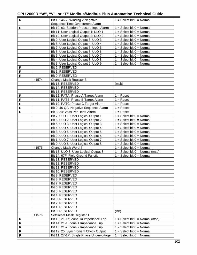
GPU 2000R “W”, “V”, or “T” Modbus/Modbus Plus Automation Technical Guide
102
R Bit 13: 46-2: Winding 2 NegativeSequence Time Overcurrent Alarm
1 = Select bit 0 = Normal
R Bit 12: 63: Sudden Pressure Input Alarm 1 = Select bit 0 = NormalBit 11: User Logical Output 1: ULO 1 1 = Select bit 0 = NormalBit 10: User Logical Output 2: ULO 2 1 = Select bit 0 = NormalBit 9: User Logical Output 3: ULO 3 1 = Select bit 0 = NormalBit 8: User Logical Output 4: ULO 4 1 = Select bit 0 = NormalBit 7: User Logical Output 5: ULO 5 1 = Select bit 0 = NormalBit 6: User Logical Output 6: ULO 6 1 = Select bit 0 = NormalBit 5: User Logical Output 7: ULO 7 1 = Select bit 0 = NormalBit 4: User Logical Output 8: ULO 8 1 = Select bit 0 = NormalBit 3: User Logical Output 9: ULO 9 1 = Select bit 0 = Normal
R Bit 2: RESERVEDR Bit 1: RESERVEDR Bit 0: RESERVED
41574 Change Mask Register 3Bit 15: RESERVED (msb)Bit 14: RESERVEDBit 13: RESERVED
R Bit 12: PATA: Phase A Target Alarm 1 = ResetR Bit 11: PATB: Phase B Target Alarm 1 = ResetR Bit 10: PATC: Phase C Target Alarm 1 = ResetR Bit 9: 46-QA: Negative Sequence Alarm 1 = ResetR Bit 8: 24: Volts Per Hertz Alarm 1 = Reset
Bit 7: ULO 1: User Logical Output 1 1 = Select bit 0 = NormalBit 6: ULO 2: User Logical Output 2 1 = Select bit 0 = NormalBit 5: ULO 3: User Logical Output 3 1 = Select bit 0 = NormalBit 4: ULO 4: User Logical Output 4 1 = Select bit 0 = NormalBit 3: ULO 5: User Logical Output 5 1 = Select bit 0 = NormalBit 2: ULO 6: User Logical Output 6 1 = Select bit 0 = NormalBit 1: ULO 7: User Logical Output 7 1 = Select bit 0 = NormalBit 0: ULO 8: User Logical Output 8 1 = Select bit 0 = Normal
41575 Change Mask Word 4 1 = Select bit 0 = NormalBit 15: ULO 8: User Logical Output 8 1 = Select bit 0 = Normal (msb)Bit 14: 67F: Field Ground Function 1 = Select bit 0 = NormalBit 13: RESERVEDBit 12: RESERVEDBit 11: RESERVEDBit 10: RESERVEDBit 9: RESERVEDBit 8: RESERVEDBit 7: RESERVEDBit 6: RESERVEDBit 5: RESERVEDBit 4: RESERVEDBit 3: RESERVEDBit 2: RESERVEDBit 1: RESERVEDBit 0: RESERVED (lsb)
41576 Set/Reset Mask Register 1R Bit 15: 21-1a: Zone 1a Impedance Trip 1 = Select bit 0 = Normal (msb)R Bit 14: 21-1: Zone 1 Impedance Trip 1 = Select bit 0 = NormalR Bit 13: 21-2: Zone 2 Impedance Trip 1 = Select bit 0 = NormalR Bit 12: 25: Synchronism Check Output 1 = Select bit 0 = NormalR Bit 11: 27-1P: Single Phase Undervoltage 1 = Select bit 0 = Normal
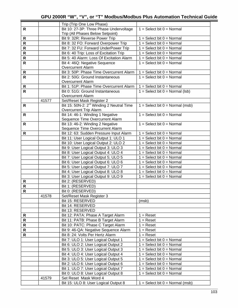
GPU 2000R “W”, “V”, or “T” Modbus/Modbus Plus Automation Technical Guide
103
Trip (Trip One Low Phase)R Bit 10: 27-3P: Three Phase Undervoltage
Trip (All Phases Below Setpoint)1 = Select bit 0 = Normal
R Bit 9: 32R: Reverse Power Trip 1 = Select bit 0 = NormalR Bit 8: 32 FO: Forward Overpower Trip 1 = Select bit 0 = NormalR Bit 7: 32 FU: Forward UnderPower Trip 1 = Select bit 0 = NormalR Bit 6: 40 Trip: Loss of Excitation Trip 1 = Select bit 0 = NormalR Bit 5: 40 Alarm: Loss Of Excitation Alarm 1 = Select bit 0 = NormalR Bit 4: 46Q: Negative Sequence
Overcurrent Alarm1 = Select bit 0 = Normal
R Bit 3: 50P: Phase Time Overcurrent Alarm 1 = Select bit 0 = NormalR Bit 2: 50G: Ground Instantaneous
Overcurrent Alarm1 = Select bit 0 = Normal
R Bit 1: 51P: Phase Time Overcurrent Alarm 1 = Select bit 0 = NormalR Bit 0: 51G: Ground Instantaneous
Overcurrent Alarm1 = Select bit 0 = Normal (lsb)
41577 Set/Reset Mask Register 2R Bit 15: 50N-2: 2nd Winding 2 Neutral Time
Overcurrent Trip Alarm1 = Select bit 0 = Normal (msb)
R Bit 14: 46-1: Winding 1 NegativeSequence Time Overcurrent Alarm
1 = Select bit 0 = Normal
R Bit 13: 46-2: Winding 2 NegativeSequence Time Overcurrent Alarm
1 = Select bit 0 = Normal
R Bit 12: 63: Sudden Pressure Input Alarm 1 = Select bit 0 = NormalBit 11: User Logical Output 1: ULO 1 1 = Select bit 0 = NormalBit 10: User Logical Output 2: ULO 2 1 = Select bit 0 = NormalBit 9: User Logical Output 3: ULO 3 1 = Select bit 0 = NormalBit 8: User Logical Output 4: ULO 4 1 = Select bit 0 = NormalBit 7: User Logical Output 5; ULO 5 1 = Select bit 0 = NormalBit 6: User Logical Output 6: ULO 6 1 = Select bit 0 = NormalBit 5: User Logical Output 7: ULO 7 1 = Select bit 0 = NormalBit 4: User Logical Output 8: ULO 8 1 = Select bit 0 = NormalBit 3: User Logical Output 9: ULO 9 1 = Select bit 0 = Normal
R Bit 2: (RESERVED)R Bit 1: (RESERVED)R Bit 0: (RESERVED)
41578 Set/Reset Mask Register 3Bit 15: RESERVED (msb)Bit 14: RESERVEDBit 13: RESERVED
R Bit 12: PATA: Phase A Target Alarm 1 = ResetR Bit 11: PATB: Phase B Target Alarm 1 = ResetR Bit 10: PATC: Phase C Target Alarm 1 = ResetR Bit 9: 46-QA: Negative Sequence Alarm 1 = ResetR Bit 8: 24: Volts Per Hertz Alarm 1 = Reset
Bit 7: ULO 1: User Logical Output 1 1 = Select bit 0 = NormalBit 6: ULO 2: User Logical Output 2 1 = Select bit 0 = NormalBit 5: ULO 3: User Logical Output 3 1 = Select bit 0 = NormalBit 4: ULO 4: User Logical Output 4 1 = Select bit 0 = NormalBit 3: ULO 5: User Logical Output 5 1 = Select bit 0 = NormalBit 2: ULO 6: User Logical Output 6 1 = Select bit 0 = NormalBit 1: ULO 7: User Logical Output 7 1 = Select bit 0 = NormalBit 0: ULO 8: User Logical Output 8 1 = Select bit 0 = Normal
41579 Set Reset Mask Word 4Bit 15: ULO 8: User Logical Output 8 1 = Select bit 0 = Normal (msb)
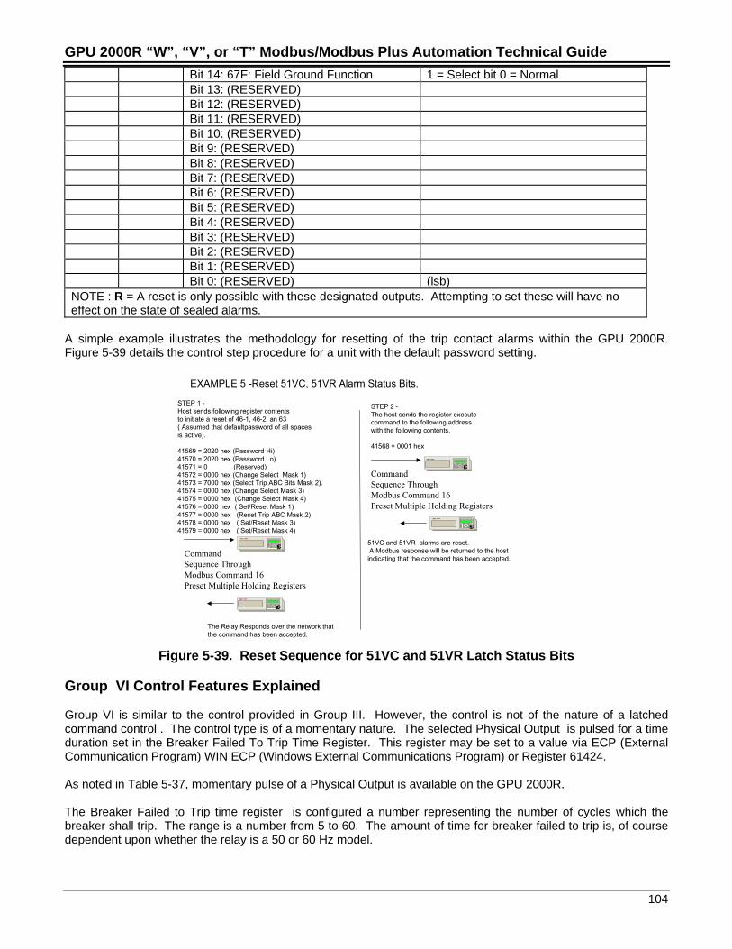
GPU 2000R “W”, “V”, or “T” Modbus/Modbus Plus Automation Technical Guide
104
Bit 14: 67F: Field Ground Function 1 = Select bit 0 = NormalBit 13: (RESERVED)Bit 12: (RESERVED)Bit 11: (RESERVED)Bit 10: (RESERVED)Bit 9: (RESERVED)Bit 8: (RESERVED)Bit 7: (RESERVED)Bit 6: (RESERVED)Bit 5: (RESERVED)Bit 4: (RESERVED)Bit 3: (RESERVED)Bit 2: (RESERVED)Bit 1: (RESERVED)Bit 0: (RESERVED) (lsb)
NOTE : R = A reset is only possible with these designated outputs. Attempting to set these will have noeffect on the state of sealed alarms.
A simple example illustrates the methodology for resetting of the trip contact alarms within the GPU 2000R.Figure 5-39 details the control step procedure for a unit with the default password setting.
ECCommandSequence ThroughModbus Command 16Preset Multiple Holding Registers
STEP 1 -Host sends following register contentsto initiate a reset of 46-1, 46-2, an 63( Assumed that defaultpassword of all spaces is active).
41569 = 2020 hex (Password Hi)41570 = 2020 hex (Password Lo)41571 = 0 (Reserved)41572 = 0000 hex (Change Select Mask 1)41573 = 7000 hex (Select Trip ABC Bits Mask 2).41574 = 0000 hex (Change Select Mask 3)41575 = 0000 hex (Change Select Mask 4)41576 = 0000 hex ( Set/Reset Mask 1)41577 = 0000 hex (Reset Trip ABC Mask 2)41578 = 0000 hex ( Set/Reset Mask 3)41579 = 0000 hex ( Set/Reset Mask 4)
EXAMPLE 5 -Reset 51VC, 51VR Alarm Status Bits.
EC
51VC and 51VR alarms are reset. A Modbus response will be returned to the hostindicating that the command has been accepted.
ECCommandSequence ThroughModbus Command 16Preset Multiple Holding Registers
STEP 2 -The host sends the register executecommand to the following address with the following contents.
41568 = 0001 hex
EC
The Relay Responds over the network that the command has been accepted.
Figure 5-39. Reset Sequence for 51VC and 51VR Latch Status Bits
Group VI Control Features Explained
Group VI is similar to the control provided in Group III. However, the control is not of the nature of a latchedcommand control . The control type is of a momentary nature. The selected Physical Output is pulsed for a timeduration set in the Breaker Failed To Trip Time Register. This register may be set to a value via ECP (ExternalCommunication Program) WIN ECP (Windows External Communications Program) or Register 61424.
As noted in Table 5-37, momentary pulse of a Physical Output is available on the GPU 2000R.
The Breaker Failed to Trip time register is configured a number representing the number of cycles which thebreaker shall trip. The range is a number from 5 to 60. The amount of time for breaker failed to trip is, of coursedependent upon whether the relay is a 50 or 60 Hz model.
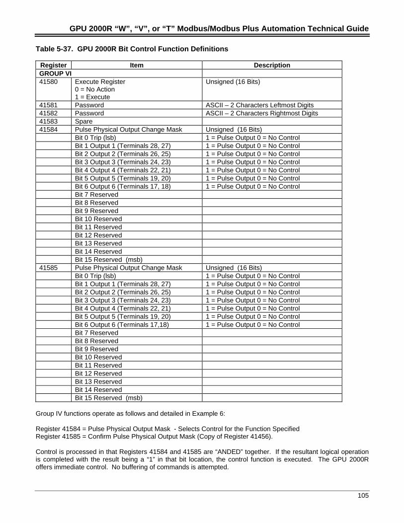
GPU 2000R “W”, “V”, or “T” Modbus/Modbus Plus Automation Technical Guide
105
Table 5-37. GPU 2000R Bit Control Function Definitions
Register Item DescriptionGROUP VI41580 Execute Register
0 = No Action1 = Execute
Unsigned (16 Bits)
41581 Password ASCII – 2 Characters Leftmost Digits41582 Password ASCII – 2 Characters Rightmost Digits41583 Spare41584 Pulse Physical Output Change Mask Unsigned (16 Bits)
Bit 0 Trip (lsb) 1 = Pulse Output 0 = No ControlBit 1 Output 1 (Terminals 28, 27) 1 = Pulse Output 0 = No ControlBit 2 Output 2 (Terminals 26, 25) 1 = Pulse Output 0 = No ControlBit 3 Output 3 (Terminals 24, 23) 1 = Pulse Output 0 = No ControlBit 4 Output 4 (Terminals 22, 21) 1 = Pulse Output 0 = No ControlBit 5 Output 5 (Terminals 19, 20) 1 = Pulse Output 0 = No ControlBit 6 Output 6 (Terminals 17, 18) 1 = Pulse Output 0 = No ControlBit 7 ReservedBit 8 ReservedBit 9 ReservedBit 10 ReservedBit 11 ReservedBit 12 ReservedBit 13 ReservedBit 14 ReservedBit 15 Reserved (msb)
41585 Pulse Physical Output Change Mask Unsigned (16 Bits)Bit 0 Trip (lsb) 1 = Pulse Output 0 = No ControlBit 1 Output 1 (Terminals 28, 27) 1 = Pulse Output 0 = No ControlBit 2 Output 2 (Terminals 26, 25) 1 = Pulse Output 0 = No ControlBit 3 Output 3 (Terminals 24, 23) 1 = Pulse Output 0 = No ControlBit 4 Output 4 (Terminals 22, 21) 1 = Pulse Output 0 = No ControlBit 5 Output 5 (Terminals 19, 20) 1 = Pulse Output 0 = No ControlBit 6 Output 6 (Terminals 17,18) 1 = Pulse Output 0 = No ControlBit 7 ReservedBit 8 ReservedBit 9 ReservedBit 10 ReservedBit 11 ReservedBit 12 ReservedBit 13 ReservedBit 14 ReservedBit 15 Reserved (msb)
Group IV functions operate as follows and detailed in Example 6:
Register 41584 = Pulse Physical Output Mask - Selects Control for the Function SpecifiedRegister 41585 = Confirm Pulse Physical Output Mask (Copy of Register 41456).
Control is processed in that Registers 41584 and 41585 are “ANDED” together. If the resultant logical operationis completed with the result being a “1” in that bit location, the control function is executed. The GPU 2000Roffers immediate control. No buffering of commands is attempted.
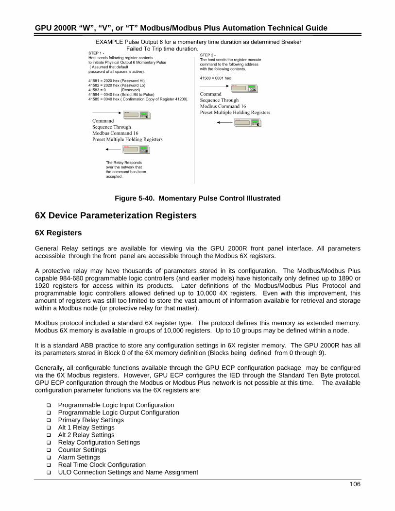
GPU 2000R “W”, “V”, or “T” Modbus/Modbus Plus Automation Technical Guide
106
ECCommandSequence ThroughModbus Command 16Preset Multiple Holding Registers
STEP 1 -Host sends following register contentsto initiate Physical Output 6 Momentary Pulse( Assumed that defaultpassword of all spaces is active).
41581 = 2020 hex (Password Hi)41582 = 2020 hex (Password Lo)41583 = 0 (Reserved)41584 = 0040 hex (Select Bit to Pulse)41585 = 0040 hex ( Confirmation Copy of Register 41200).
EXAMPLE Pulse Output 6 for a momentary time duration as determined BreakerFailed To Trip time duration.
EC
ECCommandSequence ThroughModbus Command 16Preset Multiple Holding Registers
STEP 2 -The host sends the register executecommand to the following address with the following contents.
41580 = 0001 hex
EC
The Relay Respondsover the network that the command has been accepted.
Figure 5-40. Momentary Pulse Control Illustrated
6X Device Parameterization Registers
6X Registers
General Relay settings are available for viewing via the GPU 2000R front panel interface. All parametersaccessible through the front panel are accessible through the Modbus 6X registers.
A protective relay may have thousands of parameters stored in its configuration. The Modbus/Modbus Pluscapable 984-680 programmable logic controllers (and earlier models) have historically only defined up to 1890 or1920 registers for access within its products. Later definitions of the Modbus/Modbus Plus Protocol andprogrammable logic controllers allowed defined up to 10,000 4X registers. Even with this improvement, thisamount of registers was still too limited to store the vast amount of information available for retrieval and storagewithin a Modbus node (or protective relay for that matter).
Modbus protocol included a standard 6X register type. The protocol defines this memory as extended memory.Modbus 6X memory is available in groups of 10,000 registers. Up to 10 groups may be defined within a node.
It is a standard ABB practice to store any configuration settings in 6X register memory. The GPU 2000R has allits parameters stored in Block 0 of the 6X memory definition (Blocks being defined from 0 through 9).
Generally, all configurable functions available through the GPU ECP configuration package may be configuredvia the 6X Modbus registers. However, GPU ECP configures the IED through the Standard Ten Byte protocol.GPU ECP configuration through the Modbus or Modbus Plus network is not possible at this time. The availableconfiguration parameter functions via the 6X registers are:
Programmable Logic Input Configuration Programmable Logic Output Configuration Primary Relay Settings Alt 1 Relay Settings Alt 2 Relay Settings Relay Configuration Settings Counter Settings Alarm Settings Real Time Clock Configuration ULO Connection Settings and Name Assignment
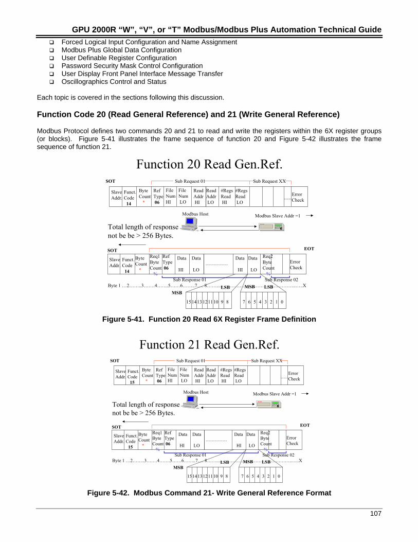
GPU 2000R “W”, “V”, or “T” Modbus/Modbus Plus Automation Technical Guide
107
Forced Logical Input Configuration and Name Assignment Modbus Plus Global Data Configuration User Definable Register Configuration Password Security Mask Control Configuration User Display Front Panel Interface Message Transfer Oscillographics Control and Status
Each topic is covered in the sections following this discussion.
Function Code 20 (Read General Reference) and 21 (Write General Reference)
Modbus Protocol defines two commands 20 and 21 to read and write the registers within the 6X register groups(or blocks). Figure 5-41 illustrates the frame sequence of function 20 and Figure 5-42 illustrates the framesequence of function 21.
Function 20 Read Gen.Ref.
Modbus Host
SlaveAddr.
Funct.Code 14
ErrorCheck
ReadAddr HI
ReadAddr LO
#RegsRead HI
#RegsRead LO
ByteCount *
RefType 06
FileNumHI
FileNum LO
Sub Request 01 Sub Request XX
EC
Modbus Slave Addr =1
SOT
SlaveAddr.
Funct.Code 14
Data
LO
Data
HI
Byte 1 …2……..3…….4…….5……6……..7…. 8……...………………………………………..…..X
Data
HI
Data
LO
ErrorCheck
ByteCount *
Req1ByteCount %
RefType 06
Sub Response 01 Sub Response 02
SOT EOT
Total length of responsenot be be > 256 Bytes.
Req2ByteCount %
MSBLSB
151413 121110 9 8 7 6 5 4 3 2 1 0
MSB LSB
Figure 5-41. Function 20 Read 6X Register Frame Definition
Function 21 Read Gen.Ref.
Modbus Host
SlaveAddr.
Funct.Code 15
ErrorCheck
ReadAddr HI
ReadAddr LO
#RegsRead HI
#RegsRead LO
ByteCount *
RefType 06
FileNumHI
FileNum LO
Sub Request 01 Sub Request XX
EC
Modbus Slave Addr =1
SOT
SlaveAddr.
Funct.Code 15
Data
LO
Data
HI
Byte 1 …2……..3…….4…….5……6……..7…. 8……...………………………………………..…..X
Data
HI
Data
LO
ErrorCheck
ByteCount *
Req1ByteCount %
RefType 06
Sub Response 01 Sub Response 02
SOT EOT
Total length of responsenot be be > 256 Bytes.
Req2ByteCount %
MSBLSB
15 1413 12 11 10 9 8 7 6 5 4 3 2 1 0
MSB LSB
Figure 5-42. Modbus Command 21- Write General Reference Format
GPU 2000R “W”, “V”, or “T” Modbus/Modbus Plus Automation Technical Guide
108
IMPLEMENTATION TIP- When 6X Registers are written, a 10 minute execute timer is initiated upon thefirst write to a 6X block. If the execute register is not written with a value of 1 within the 10 minutes of theinitial write, the 6X viewable register segment will be restored to the original values from the GPU 2000Rinternal flash ram memory.
Programmable Input Configuration
The GPU 2000R allows for query or changing of Relay Configuration Data via the Modbus ASCII protocol. Table5-38 further describes the register assignment for viewing or changing the GPU 2000R parameters.
Term Definitions
The parameterization may be configured via ECP or WIN ECP. However changing the Programmable InputConfiguration is slightly more involved through Modbus Plus or Modbus. A few terms must be understood beforediscussing the procedure for changing the 6X memory Programmable Input parameters.
Physical Input: The opto-isolated binary input that allows external control by physically wiring the inputterminals of the GPU2000R. Physical inputs are labeled (IN1, IN2, IN3 …. IN8).
Logical Input: An input equated by the boolean combination of the physical inputs. These inputs are usedby the GPU2000R's state machine and control subroutines. Logical Inputs are labeled
Active Open: This defines the type of connection from the physical input or inputs and means the physicalstate of the opto-isolator's logic is inverted. Example: if the voltage across IN1's terminals equals zero,then the boolean equation will evaluate this term as a logical one. Likewise, when a voltage is appliedto IN1, the boolean equation will evaluate this term as a logical zero.
Active Closed: This defines the type of connection from the physical input or inputs and means that thephysical state of the opto-isolator's logic is the non-inverted. Example: if a voltage is applied acrossIN1's terminals, then the boolean equation will evaluate this term as a logical one. Likewise, when avoltage is applied to IN1, the boolean equation will evaluate this term as a logical zero.
Boolean Logic Input Equation:
Logical ORed Physical50 P = IN1 + IN2 + IN3
Logical ANDed Physical50 G = IN1 * IN2 * IN3
Input Select:The physical inputs are associated with a bit mask to determine which inputs are used whenresolving the logical input's boolean equation. If the appropriate bit is set, the term will be includedas part of the equation. Likewise, a cleared bit indicates that the physical input term will be ignored.
0= IN1 1= IN 2 2 = IN3, 3 = IN4, 4 = IN5, 5 = IN6, 6 = IN 7, 7 = IN8, ALL OTHER BITS ARERESERVED.
Negated AND Input:This is a bit mask that indicates if a selected input is inverted based on the active open or closed state.The bit mask uses the same associated physical inputs pattern as in the Input Select data.
0= IN1 1= IN 2 2 = IN3, 3 = IN4, 4 = IN5, 5 = IN6, 6 = IN 7, 7 = IN8, ALL OTHER BITS ARERESERVED.
GPU 2000R “W”, “V”, or “T” Modbus/Modbus Plus Automation Technical Guide
109
AND/OR Select:The combination of the physical inputs' state used to resolve the boolean equation allows for thealgebraic ANDing or ORing of all of the selected physical inputs.
The bit mapping for the logical inputs are as follows:
0= INPUT 1, 1= INPUT 2, 3 = INPUT 3, ……..29 = INPUT 30, 30=INPUT 31, 31=INPUT 32
User Definable Names:Physical inputs, IN1 - IN13, have memory allocated for an eight character (NULL is implied incharacter 9) user definable strings.
Methodology and Register Manipulation to Configure the Programmable Logical Input
Four protocol commands are required to view or change the GPU 2000R's programmable input setting tables. Thecommand order for viewing these tables can be retrieved in any sequence, but when the settings are sent to theGPU2000, the commands must be sent in the following sequence:
Receive Programmable Input Select and Index data.Receive Programmable Negated AND Input data.
Receive Programmable Input AND/OR Select data.Receive Programmable Input User Defined Name data.
Up to 29 logical inputs may be selected at any one time. The protocol document refers to these generic logical inputsas INPUT1 – INPUT32.
Tables X through XX are used to configure the boolean algebraic equations for the desired configuration:
An example illustrating the configuration technique shall suffice:
EXAMPLE:
We wish to define the XXX logical input to be the combination of the physical inputs IN4 AND (NOT IN3) and to definethe YYY logical input to be the combination of the physical inputs IN1 OR IN3 OR (NOT IN5), which is denoted:
XXX = IN4 *( !IN3)
YYY = IN1 + IN3 + (!IN5)
SOLUTION:
First, generic inputs must be selected to setup the logic equation, and for this case INPUT3 is used for XXX andINPUT8 is used for YYY. Note that any logical inputs 1-32 could be valid selections. The data values required for theselections XXX and YYY use the INDEX table defined in the protocol document.
Register HexData Comment60007 0xFFF3 No physicals selected for INPUT3 Input Select high byte
Selects IN3 and IN4 bits for INPUT3 Input Select low byte60045 0x???? Assigning “XXX” offset to INPUT3 for Input Index high byte60012 0xFFEE No physicals selected for INPUT3 Input Select high byte
Selects IN1 and IN5 bits for INPUT8 Input Select low byte60047 0x???? Assigning “YYY” offset to INPUT8 for Input Index low byte60066 0xFFFB No physical's logic inverted for INPUT3 Negated AND Input high byte
Inverts IN3's logical state for INPUT3 Negated AND Input low byte60071 0xFFEF No physical's logic inverted for INPUT8 Negated AND Input high byte
Inverts IN5's logical state for INPUT8 Negated AND Input low byte
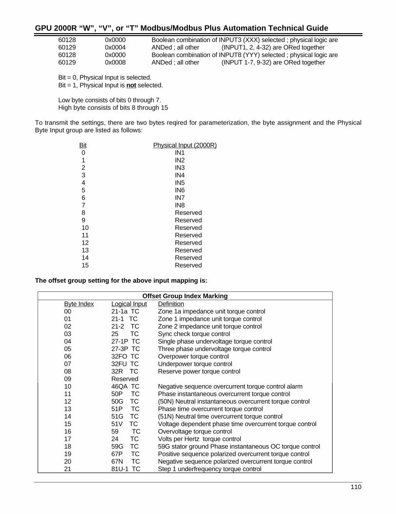
GPU 2000R “W”, “V”, or “T” Modbus/Modbus Plus Automation Technical Guide
110
60128 0x0000 Boolean combination of INPUT3 (XXX) selected ; physical logic are60129 0x0004 ANDed ; all other (INPUT1, 2, 4-32) are ORed together60128 0x0000 Boolean combination of INPUT8 (YYY) selected ; physical logic are60129 0x0008 ANDed ; all other (INPUT 1-7, 9-32) are ORed together
Bit = 0, Physical Input is selected.Bit = 1, Physical Input is not selected.
Low byte consists of bits 0 through 7.High byte consists of bits 8 through 15
To transmit the settings, there are two bytes reqired for parameterization, the byte assignment and the PhysicalByte Input group are listed as follows:
Bit Physical Input (2000R) 0 IN1 1 IN2 2 IN3 3 IN4
4 IN5 5 IN6
6 IN77 IN88 Reserved
9 Reserved10 Reserved11 Reserved12 Reserved
13 Reserved 14 Reserved
15 Reserved
The offset group setting for the above input mapping is:
Offset Group Index MarkingByte Index Logical Input Definition00 21-1a TC Zone 1a impedance unit torque control01 21-1 TC Zone 1 impedance unit torque control02 21-2 TC Zone 2 impedance unit torque control03 25 TC Sync check torque control04 27-1P TC Single phase undervoltage torque control05 27-3P TC Three phase undervoltage torque control06 32FO TC Overpower torque control07 32FU TC Underpower torque control08 32R TC Reserve power torque control09 Reserved10 46QA TC Negative sequence overcurrent torque control alarm11 50P TC Phase instantaneous overcurrent torque control12 50G TC (50N) Neutral instantaneous overcurrent torque control13 51P TC Phase time overcurrent torque control14 51G TC (51N) Neutral time overcurrent torque control15 51V TC Voltage dependent phase time overcurrent torque control16 59 TC Overvoltage torque control17 24 TC Volts per Hertz torque control18 59G TC 59G stator ground Phase instantaneous OC torque control19 67P TC Positive sequence polarized overcurrent torque control20 67N TC Negative sequence polarized overcurrent torque control21 81U-1 TC Step 1 underfrequency torque control
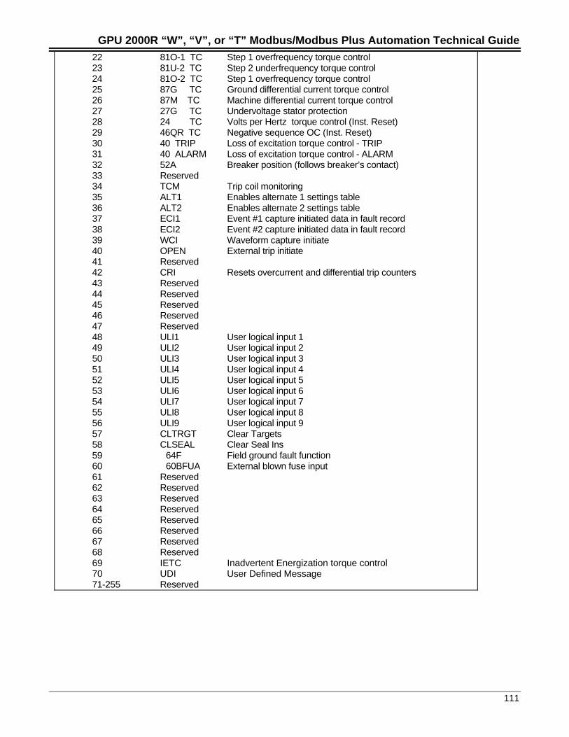
GPU 2000R “W”, “V”, or “T” Modbus/Modbus Plus Automation Technical Guide
111
22 81O-1 TC Step 1 overfrequency torque control23 81U-2 TC Step 2 underfrequency torque control24 81O-2 TC Step 1 overfrequency torque control25 87G TC Ground differential current torque control26 87M TC Machine differential current torque control27 27G TC Undervoltage stator protection28 24 TC Volts per Hertz torque control (Inst. Reset)29 46QR TC Negative sequence OC (Inst. Reset)30 40 TRIP Loss of excitation torque control - TRIP31 40 ALARM Loss of excitation torque control - ALARM32 52A Breaker position (follows breaker’s contact)33 Reserved34 TCM Trip coil monitoring35 ALT1 Enables alternate 1 settings table36 ALT2 Enables alternate 2 settings table37 ECI1 Event #1 capture initiated data in fault record38 ECI2 Event #2 capture initiated data in fault record39 WCI Waveform capture initiate40 OPEN External trip initiate41 Reserved42 CRI Resets overcurrent and differential trip counters43 Reserved44 Reserved45 Reserved46 Reserved47 Reserved48 ULI1 User logical input 149 ULI2 User logical input 250 ULI3 User logical input 351 ULI4 User logical input 452 ULI5 User logical input 553 ULI6 User logical input 654 ULI7 User logical input 755 ULI8 User logical input 856 ULI9 User logical input 957 CLTRGT Clear Targets58 CLSEAL Clear Seal Ins59 64F Field ground fault function60 60BFUA External blown fuse input61 Reserved62 Reserved63 Reserved64 Reserved65 Reserved66 Reserved67 Reserved68 Reserved69 IETC Inadvertent Energization torque control70 UDI User Defined Message71-255 Reserved
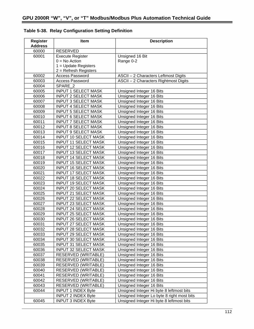
GPU 2000R “W”, “V”, or “T” Modbus/Modbus Plus Automation Technical Guide
112
Table 5-38. Relay Configuration Setting Definition
RegisterAddress
Item Description
60000 RESERVED60001 Execute Register
0 = No Action1 = Update Registers2 = Refresh Registers
Unsigned 16 BitRange 0-2
60002 Access Password ASCII – 2 Characters Leftmost Digits60003 Access Password ASCII – 2 Characters Rightmost Digits60004 SPARE_260005 INPUT 1 SELECT MASK Unsigned Integer 16 Bits60006 INPUT 2 SELECT MASK Unsigned Integer 16 Bits60007 INPUT 3 SELECT MASK Unsigned Integer 16 Bits60008 INPUT 4 SELECT MASK Unsigned Integer 16 Bits60009 INPUT 5 SELECT MASK Unsigned Integer 16 Bits60010 INPUT 6 SELECT MASK Unsigned Integer 16 Bits60011 INPUT 7 SELECT MASK Unsigned Integer 16 Bits60012 INPUT 8 SELECT MASK Unsigned Integer 16 Bits60013 INPUT 9 SELECT MASK Unsigned Integer 16 Bits60014 INPUT 10 SELECT MASK Unsigned Integer 16 Bits60015 INPUT 11 SELECT MASK Unsigned Integer 16 Bits60016 INPUT 12 SELECT MASK Unsigned Integer 16 Bits60017 INPUT 13 SELECT MASK Unsigned Integer 16 Bits60018 INPUT 14 SELECT MASK Unsigned Integer 16 Bits60019 INPUT 15 SELECT MASK Unsigned Integer 16 Bits60020 INPUT 16 SELECT MASK Unsigned Integer 16 Bits60021 INPUT 17 SELECT MASK Unsigned Integer 16 Bits60022 INPUT 18 SELECT MASK Unsigned Integer 16 Bits60023 INPUT 19 SELECT MASK Unsigned Integer 16 Bits60024 INPUT 20 SELECT MASK Unsigned Integer 16 Bits60025 INPUT 21 SELECT MASK Unsigned Integer 16 Bits60026 INPUT 22 SELECT MASK Unsigned Integer 16 Bits60027 INPUT 23 SELECT MASK Unsigned Integer 16 Bits60028 INPUT 24 SELECT MASK Unsigned Integer 16 Bits60029 INPUT 25 SELECT MASK Unsigned Integer 16 Bits60030 INPUT 26 SELECT MASK Unsigned Integer 16 Bits60031 INPUT 27 SELECT MASK Unsigned Integer 16 Bits60032 INPUT 28 SELECT MASK Unsigned Integer 16 Bits60033 INPUT 29 SELECT MASK Unsigned Integer 16 Bits60034 INPUT 30 SELECT MASK Unsigned Integer 16 Bits60035 INPUT 31 SELECT MASK Unsigned Integer 16 Bits60036 INPUT 32 SELECT MASK Unsigned Integer 16 Bits60037 RESERVED (WRITABLE) Unsigned Integer 16 Bits60038 RESERVED (WRITABLE) Unsigned Integer 16 Bits60039 RESERVED (WRITABLE) Unsigned Integer 16 Bits60040 RESERVED (WRITABLE) Unsigned Integer 16 Bits60041 RESERVED (WRITABLE) Unsigned Integer 16 Bits60042 RESERVED (WRITABLE) Unsigned Integer 16 Bits60043 RESERVED (WRITABLE) Unsigned Integer 16 Bits60044 INPUT 1 INDEX Byte Unsigned Integer Hi byte 8 leftmost bits
INPUT 2 INDEX Byte Unsigned Integer Lo byte 8 right most bits60045 INPUT 3 INDEX Byte Unsigned Integer Hi byte 8 leftmost bits
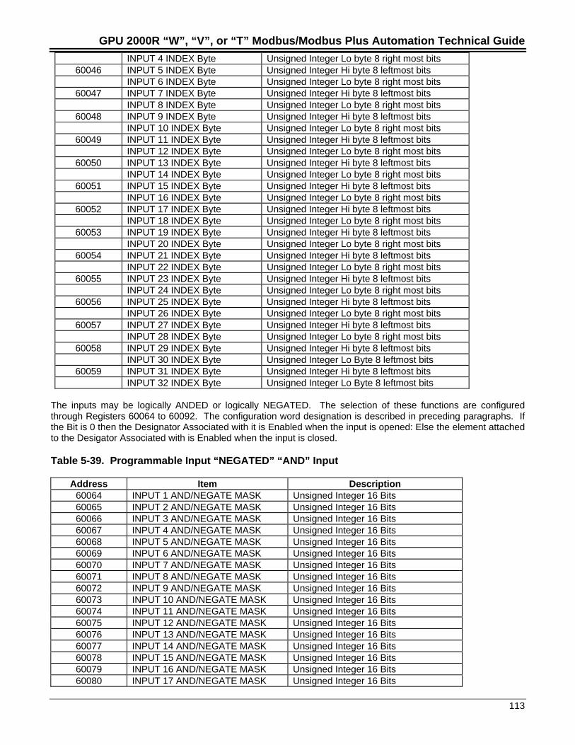
GPU 2000R “W”, “V”, or “T” Modbus/Modbus Plus Automation Technical Guide
113
INPUT 4 INDEX Byte Unsigned Integer Lo byte 8 right most bits60046 INPUT 5 INDEX Byte Unsigned Integer Hi byte 8 leftmost bits
INPUT 6 INDEX Byte Unsigned Integer Lo byte 8 right most bits60047 INPUT 7 INDEX Byte Unsigned Integer Hi byte 8 leftmost bits
INPUT 8 INDEX Byte Unsigned Integer Lo byte 8 right most bits60048 INPUT 9 INDEX Byte Unsigned Integer Hi byte 8 leftmost bits
INPUT 10 INDEX Byte Unsigned Integer Lo byte 8 right most bits60049 INPUT 11 INDEX Byte Unsigned Integer Hi byte 8 leftmost bits
INPUT 12 INDEX Byte Unsigned Integer Lo byte 8 right most bits60050 INPUT 13 INDEX Byte Unsigned Integer Hi byte 8 leftmost bits
INPUT 14 INDEX Byte Unsigned Integer Lo byte 8 right most bits60051 INPUT 15 INDEX Byte Unsigned Integer Hi byte 8 leftmost bits
INPUT 16 INDEX Byte Unsigned Integer Lo byte 8 right most bits60052 INPUT 17 INDEX Byte Unsigned Integer Hi byte 8 leftmost bits
INPUT 18 INDEX Byte Unsigned Integer Lo byte 8 right most bits60053 INPUT 19 INDEX Byte Unsigned Integer Hi byte 8 leftmost bits
INPUT 20 INDEX Byte Unsigned Integer Lo byte 8 right most bits60054 INPUT 21 INDEX Byte Unsigned Integer Hi byte 8 leftmost bits
INPUT 22 INDEX Byte Unsigned Integer Lo byte 8 right most bits60055 INPUT 23 INDEX Byte Unsigned Integer Hi byte 8 leftmost bits
INPUT 24 INDEX Byte Unsigned Integer Lo byte 8 right most bits60056 INPUT 25 INDEX Byte Unsigned Integer Hi byte 8 leftmost bits
INPUT 26 INDEX Byte Unsigned Integer Lo byte 8 right most bits60057 INPUT 27 INDEX Byte Unsigned Integer Hi byte 8 leftmost bits
INPUT 28 INDEX Byte Unsigned Integer Lo byte 8 right most bits60058 INPUT 29 INDEX Byte Unsigned Integer Hi byte 8 leftmost bits
INPUT 30 INDEX Byte Unsigned Integer Lo Byte 8 leftmost bits60059 INPUT 31 INDEX Byte Unsigned Integer Hi byte 8 leftmost bits
INPUT 32 INDEX Byte Unsigned Integer Lo Byte 8 leftmost bits
The inputs may be logically ANDED or logically NEGATED. The selection of these functions are configuredthrough Registers 60064 to 60092. The configuration word designation is described in preceding paragraphs. Ifthe Bit is 0 then the Designator Associated with it is Enabled when the input is opened: Else the element attachedto the Desigator Associated with is Enabled when the input is closed.
Table 5-39. Programmable Input “NEGATED” “AND” Input
Address Item Description60064 INPUT 1 AND/NEGATE MASK Unsigned Integer 16 Bits60065 INPUT 2 AND/NEGATE MASK Unsigned Integer 16 Bits60066 INPUT 3 AND/NEGATE MASK Unsigned Integer 16 Bits60067 INPUT 4 AND/NEGATE MASK Unsigned Integer 16 Bits60068 INPUT 5 AND/NEGATE MASK Unsigned Integer 16 Bits60069 INPUT 6 AND/NEGATE MASK Unsigned Integer 16 Bits60070 INPUT 7 AND/NEGATE MASK Unsigned Integer 16 Bits60071 INPUT 8 AND/NEGATE MASK Unsigned Integer 16 Bits60072 INPUT 9 AND/NEGATE MASK Unsigned Integer 16 Bits60073 INPUT 10 AND/NEGATE MASK Unsigned Integer 16 Bits60074 INPUT 11 AND/NEGATE MASK Unsigned Integer 16 Bits60075 INPUT 12 AND/NEGATE MASK Unsigned Integer 16 Bits60076 INPUT 13 AND/NEGATE MASK Unsigned Integer 16 Bits60077 INPUT 14 AND/NEGATE MASK Unsigned Integer 16 Bits60078 INPUT 15 AND/NEGATE MASK Unsigned Integer 16 Bits60079 INPUT 16 AND/NEGATE MASK Unsigned Integer 16 Bits60080 INPUT 17 AND/NEGATE MASK Unsigned Integer 16 Bits
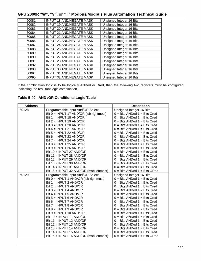
GPU 2000R “W”, “V”, or “T” Modbus/Modbus Plus Automation Technical Guide
114
60081 INPUT 18 AND/NEGATE MASK Unsigned Integer 16 Bits60082 INPUT 19 AND/NEGATE MASK Unsigned Integer 16 Bits60083 INPUT 20 AND/NEGATE MASK Unsigned Integer 16 Bits60084 INPUT 21 AND/NEGATE MASK Unsigned Integer 16 Bits60085 INPUT 22 AND/NEGATE MASK Unsigned Integer 16 Bits60086 INPUT 23 AND/NEGATE MASK Unsigned Integer 16 Bits60087 INPUT 24 AND/NEGATE MASK Unsigned Integer 16 Bits60088 INPUT 25 AND/NEGATE MASK Unsigned Integer 16 Bits60089 INPUT 26 AND/NEGATE MASK Unsigned Integer 16 Bits60090 INPUT 27 AND/NEGATE MASK Unsigned Integer 16 Bits60091 INPUT 28 AND/NEGATE MASK Unsigned Integer 16 Bits60092 INPUT 29 AND/NEGATE MASK Unsigned Integer 16 Bits60093 INPUT 30 AND/NEGATE MASK Unsigned Integer 16 Bits60094 INPUT 31 AND/NEGATE MASK Unsigned Integer 16 Bits60095 INPUT 32 AND/NEGATE MASK Unsigned Integer 16 Bits
If the combination logic is to be logically ANDed or Ored, then the following two registers must be configuredindicating the resultant logic combination.
Table 5-40. AND /OR Conditional Logic Table
Address Item Description60128 Programmable Input And/OR Select
Bit 0 = INPUT 17 AND/OR (lsb rightmost)Bit 1 = INPUT 18 AND/ORBit 2 = INPUT 19 AND/ORBit 3 = INPUT 20 AND/ORBit 4 = INPUT 21 AND/ORBit 5 = INPUT 22 AND/ORBit 6 = INPUT 23 AND/ORBit 7 = INPUT 24 AND/ORBit 8 = INPUT 25 AND/ORBit 9 = INPUT 26 AND/ORBit 10 = INPUT 27 AND/ORBit 11 = INPUT 28 AND/ORBit 12 = INPUT 29 AND/ORBit 13 = INPUT 30 AND/ORBit 14 = INPUT 31 AND/ORBit 15 = INPUT 32 AND/OR (msb leftmost)
Unsigned Integer 16 Bits0 = Bits ANDed 1 = Bits Ored0 = Bits ANDed 1 = Bits Ored0 = Bits ANDed 1 = Bits Ored0 = Bits ANDed 1 = Bits Ored0 = Bits ANDed 1 = Bits Ored0 = Bits ANDed 1 = Bits Ored0 = Bits ANDed 1 = Bits Ored0 = Bits ANDed 1 = Bits Ored0 = Bits ANDed 1 = Bits Ored0 = Bits ANDed 1 = Bits Ored0 = Bits ANDed 1 = Bits Ored0 = Bits ANDed 1 = Bits Ored0 = Bits ANDed 1 = Bits Ored0 = Bits ANDed 1 = Bits Ored0 = Bits ANDed 1 = Bits Ored0 = Bits ANDed 1 = Bits ORed
60129 Programmable Input And/OR SelectBit 0 = INPUT 1 AND/OR (lsb rightmost)Bit 1 = INPUT 2 AND/ORBit 2 = INPUT 3 AND/ORBit 3 = INPUT 4 AND/ORBit 4 = INPUT 5 AND/ORBit 5 = INPUT 6 AND/ORBit 6 = INPUT 7 AND/ORBit 7 = INPUT 8 AND/ORBit 8 = INPUT 9 AND/ORBit 9 = INPUT 10 AND/ORBit 10 = INPUT 11 AND/ORBit 11 = INPUT 12 AND/ORBit 12 = INPUT 13 AND/ORBit 13 = INPUT 14 AND/ORBit 14 = INPUT 15 AND/ORBit 15 = INPUT 16 AND/OR (msb leftmost)
Unsigned Integer 16 Bits0 = Bits ANDed 1 = Bits Ored0 = Bits ANDed 1 = Bits Ored0 = Bits ANDed 1 = Bits Ored0 = Bits ANDed 1 = Bits Ored0 = Bits ANDed 1 = Bits Ored0 = Bits ANDed 1 = Bits Ored0 = Bits ANDed 1 = Bits Ored0 = Bits ANDed 1 = Bits Ored0 = Bits ANDed 1 = Bits Ored0 = Bits ANDed 1 = Bits Ored0 = Bits ANDed 1 = Bits Ored0 = Bits ANDed 1 = Bits Ored0 = Bits ANDed 1 = Bits Ored0 = Bits ANDed 1 = Bits Ored0 = Bits ANDed 1 = Bits Ored0 = Bits ANDed 1 = Bits ORed
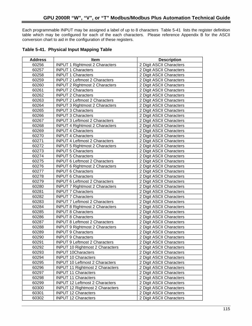
GPU 2000R “W”, “V”, or “T” Modbus/Modbus Plus Automation Technical Guide
115
Each programmable INPUT may be assigned a label of up to 8 characters Table 5-41 lists the register definitiontable which may be configured for each of the each characters. Please reference Appendix B for the ASCIIconversion chart to aid in the configuration of these registers.
Table 5-41. Physical Input Mapping Table
Address Item Description60256 INPUT 1 Rightmost 2 Characters 2 Digit ASCII Characters60257 INPUT 1 Characters 2 Digit ASCII Characters60258 INPUT 1 Characters 2 Digit ASCII Characters60259 INPUT 2 Leftmost 2 Characters 2 Digit ASCII Characters60260 INPUT 2 Rightmost 2 Characters 2 Digit ASCII Characters60261 INPUT 2 Characters 2 Digit ASCII Characters60262 INPUT 2 Characters 2 Digit ASCII Characters60263 INPUT 2 Leftmost 2 Characters 2 Digit ASCII Characters60264 INPUT 3 Rightmost 2 Characters 2 Digit ASCII Characters60265 INPUT 3 Characters 2 Digit ASCII Characters60266 INPUT 3 Characters 2 Digit ASCII Characters60267 INPUT 3 Leftmost 2 Characters 2 Digit ASCII Characters60268 INPUT 4 Rightmost 2 Characters 2 Digit ASCII Characters60269 INPUT 4 Characters 2 Digit ASCII Characters60270 INPUT 4 Characters 2 Digit ASCII Characters60271 INPUT 4 Leftmost 2 Characters 2 Digit ASCII Characters60272 INPUT 5 Rightmost 2 Characters 2 Digit ASCII Characters60273 INPUT 5 Characters 2 Digit ASCII Characters60274 INPUT 5 Characters 2 Digit ASCII Characters60275 INPUT 6 Leftmost 2 Characters 2 Digit ASCII Characters60276 INPUT 6 Rightmost 2 Characters 2 Digit ASCII Characters60277 INPUT 6 Characters 2 Digit ASCII Characters60278 INPUT 6 Characters 2 Digit ASCII Characters60279 INPUT 6 Leftmost 2 Characters 2 Digit ASCII Characters60280 INPUT 7 Rightmost 2 Characters 2 Digit ASCII Characters60281 INPUT 7 Characters 2 Digit ASCII Characters60282 INPUT 7 Characters 2 Digit ASCII Characters60283 INPUT 7 Leftmost 2 Characters 2 Digit ASCII Characters60284 INPUT 8 Rightmost 2 Characters 2 Digit ASCII Characters60285 INPUT 8 Characters 2 Digit ASCII Characters60286 INPUT 8 Characters 2 Digit ASCII Characters60287 INPUT 8 Leftmost 2 Characters 2 Digit ASCII Characters60288 INPUT 9 Rightmost 2 Characters 2 Digit ASCII Characters60289 INPUT 9 Characters 2 Digit ASCII Characters60290 INPUT 9 Characters 2 Digit ASCII Characters60291 INPUT 9 Leftmost 2 Characters 2 Digit ASCII Characters60292 INPUT 10 Rightmost 2 Characters 2 Digit ASCII Characters60293 INPUT 10Characters 2 Digit ASCII Characters60294 INPUT 10 Characters 2 Digit ASCII Characters60295 INPUT 10 Leftmost 2 Characters 2 Digit ASCII Characters60296 INPUT 11 Rightmost 2 Characters 2 Digit ASCII Characters60297 INPUT 11 Characters 2 Digit ASCII Characters60298 INPUT 11 Characters 2 Digit ASCII Characters60299 INPUT 12 Leftmost 2 Characters 2 Digit ASCII Characters60300 INPUT 12 Rightmost 2 Characters 2 Digit ASCII Characters60301 INPUT 12 Characters 2 Digit ASCII Characters60302 INPUT 12 Characters 2 Digit ASCII Characters
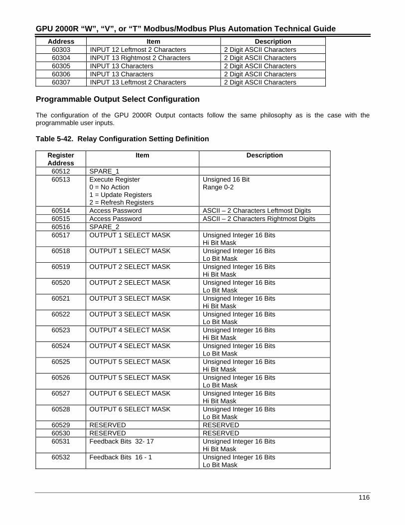
GPU 2000R “W”, “V”, or “T” Modbus/Modbus Plus Automation Technical Guide
116
Address Item Description60303 INPUT 12 Leftmost 2 Characters 2 Digit ASCII Characters60304 INPUT 13 Rightmost 2 Characters 2 Digit ASCII Characters60305 INPUT 13 Characters 2 Digit ASCII Characters60306 INPUT 13 Characters 2 Digit ASCII Characters60307 INPUT 13 Leftmost 2 Characters 2 Digit ASCII Characters
Programmable Output Select Configuration
The configuration of the GPU 2000R Output contacts follow the same philosophy as is the case with theprogrammable user inputs.
Table 5-42. Relay Configuration Setting Definition
RegisterAddress
Item Description
60512 SPARE_160513 Execute Register
0 = No Action1 = Update Registers2 = Refresh Registers
Unsigned 16 BitRange 0-2
60514 Access Password ASCII – 2 Characters Leftmost Digits60515 Access Password ASCII – 2 Characters Rightmost Digits60516 SPARE_260517 OUTPUT 1 SELECT MASK Unsigned Integer 16 Bits
Hi Bit Mask60518 OUTPUT 1 SELECT MASK Unsigned Integer 16 Bits
Lo Bit Mask60519 OUTPUT 2 SELECT MASK Unsigned Integer 16 Bits
Hi Bit Mask60520 OUTPUT 2 SELECT MASK Unsigned Integer 16 Bits
Lo Bit Mask60521 OUTPUT 3 SELECT MASK Unsigned Integer 16 Bits
Hi Bit Mask60522 OUTPUT 3 SELECT MASK Unsigned Integer 16 Bits
Lo Bit Mask60523 OUTPUT 4 SELECT MASK Unsigned Integer 16 Bits
Hi Bit Mask60524 OUTPUT 4 SELECT MASK Unsigned Integer 16 Bits
Lo Bit Mask60525 OUTPUT 5 SELECT MASK Unsigned Integer 16 Bits
Hi Bit Mask60526 OUTPUT 5 SELECT MASK Unsigned Integer 16 Bits
Lo Bit Mask60527 OUTPUT 6 SELECT MASK Unsigned Integer 16 Bits
Hi Bit Mask60528 OUTPUT 6 SELECT MASK Unsigned Integer 16 Bits
Lo Bit Mask60529 RESERVED RESERVED60530 RESERVED RESERVED60531 Feedback Bits 32- 17 Unsigned Integer 16 Bits
Hi Bit Mask60532 Feedback Bits 16 - 1 Unsigned Integer 16 Bits
Lo Bit Mask
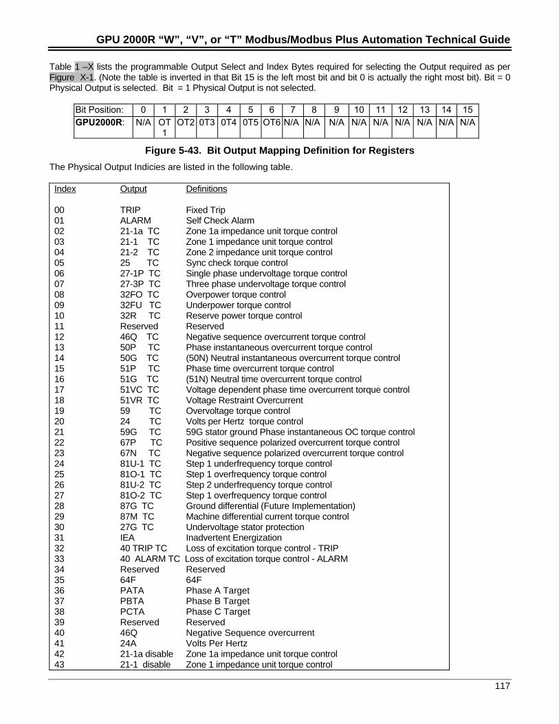
GPU 2000R “W”, “V”, or “T” Modbus/Modbus Plus Automation Technical Guide
117
Table 1 –X lists the programmable Output Select and Index Bytes required for selecting the Output required as perFigure X-1. (Note the table is inverted in that Bit 15 is the left most bit and bit 0 is actually the right most bit). Bit = 0Physical Output is selected. Bit = 1 Physical Output is not selected.
Bit Position: 0 1 2 3 4 5 6 7 8 9 10 11 12 13 14 15GPU2000R: N/A OT
1OT2 0T3 0T4 0T5 OT6 N/A N/A N/A N/A N/A N/A N/A N/A N/A
Figure 5-43. Bit Output Mapping Definition for Registers
The Physical Output Indicies are listed in the following table.
Index Output Definitions
00 TRIP Fixed Trip01 ALARM Self Check Alarm02 21-1a TC Zone 1a impedance unit torque control03 21-1 TC Zone 1 impedance unit torque control04 21-2 TC Zone 2 impedance unit torque control05 25 TC Sync check torque control06 27-1P TC Single phase undervoltage torque control07 27-3P TC Three phase undervoltage torque control08 32FO TC Overpower torque control09 32FU TC Underpower torque control10 32R TC Reserve power torque control11 Reserved Reserved12 46Q TC Negative sequence overcurrent torque control13 50P TC Phase instantaneous overcurrent torque control14 50G TC (50N) Neutral instantaneous overcurrent torque control15 51P TC Phase time overcurrent torque control16 51G TC (51N) Neutral time overcurrent torque control17 51VC TC Voltage dependent phase time overcurrent torque control18 51VR TC Voltage Restraint Overcurrent19 59 TC Overvoltage torque control20 24 TC Volts per Hertz torque control21 59G TC 59G stator ground Phase instantaneous OC torque control22 67P TC Positive sequence polarized overcurrent torque control23 67N TC Negative sequence polarized overcurrent torque control24 81U-1 TC Step 1 underfrequency torque control25 81O-1 TC Step 1 overfrequency torque control26 81U-2 TC Step 2 underfrequency torque control27 81O-2 TC Step 1 overfrequency torque control28 87G TC Ground differential (Future Implementation)29 87M TC Machine differential current torque control30 27G TC Undervoltage stator protection31 IEA Inadvertent Energization32 40 TRIP TC Loss of excitation torque control - TRIP33 40 ALARM TC Loss of excitation torque control - ALARM34 Reserved Reserved35 64F 64F36 PATA Phase A Target37 PBTA Phase B Target38 PCTA Phase C Target39 Reserved Reserved40 46Q Negative Sequence overcurrent41 24A Volts Per Hertz42 21-1a disable Zone 1a impedance unit torque control43 21-1 disable Zone 1 impedance unit torque control
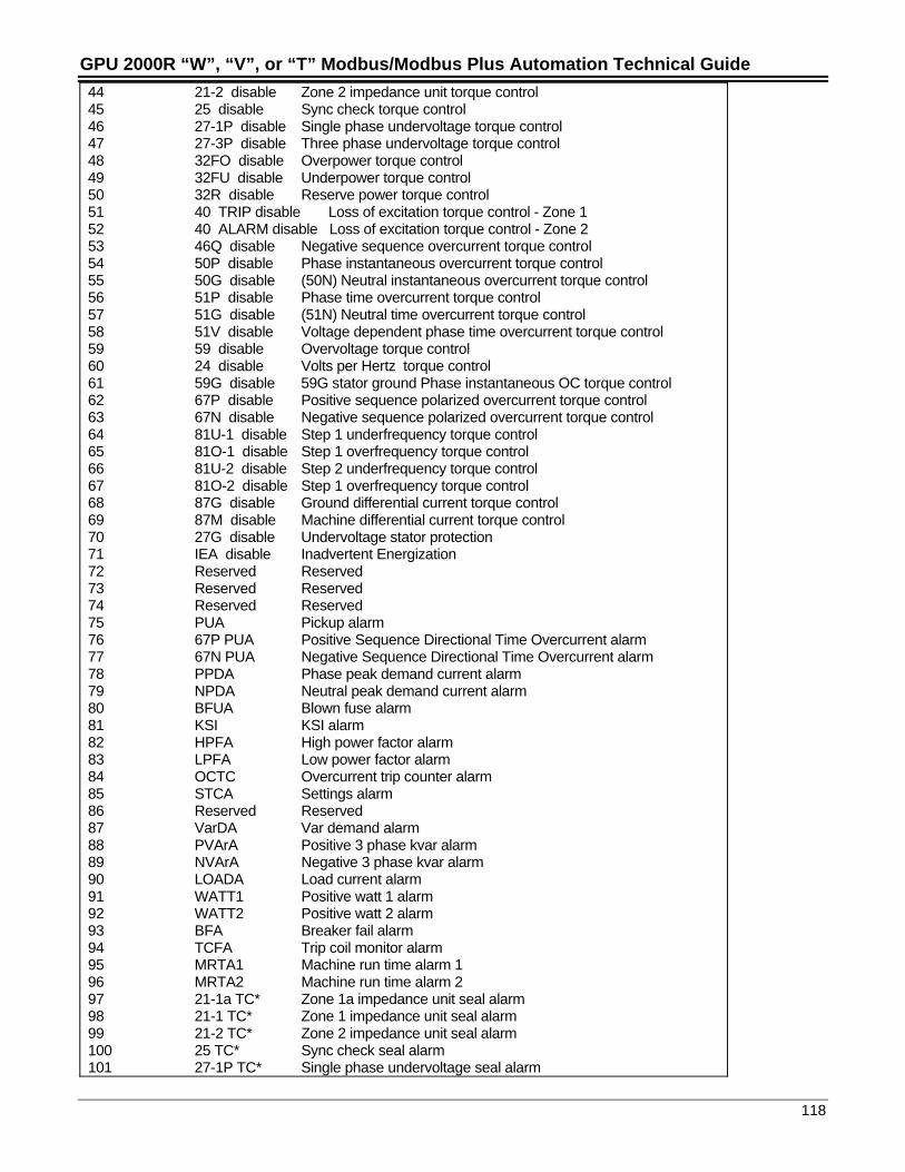
GPU 2000R “W”, “V”, or “T” Modbus/Modbus Plus Automation Technical Guide
118
44 21-2 disable Zone 2 impedance unit torque control45 25 disable Sync check torque control46 27-1P disable Single phase undervoltage torque control47 27-3P disable Three phase undervoltage torque control48 32FO disable Overpower torque control49 32FU disable Underpower torque control50 32R disable Reserve power torque control51 40 TRIP disable Loss of excitation torque control - Zone 152 40 ALARM disable Loss of excitation torque control - Zone 253 46Q disable Negative sequence overcurrent torque control54 50P disable Phase instantaneous overcurrent torque control55 50G disable (50N) Neutral instantaneous overcurrent torque control56 51P disable Phase time overcurrent torque control57 51G disable (51N) Neutral time overcurrent torque control58 51V disable Voltage dependent phase time overcurrent torque control59 59 disable Overvoltage torque control60 24 disable Volts per Hertz torque control61 59G disable 59G stator ground Phase instantaneous OC torque control62 67P disable Positive sequence polarized overcurrent torque control63 67N disable Negative sequence polarized overcurrent torque control64 81U-1 disable Step 1 underfrequency torque control65 81O-1 disable Step 1 overfrequency torque control66 81U-2 disable Step 2 underfrequency torque control67 81O-2 disable Step 1 overfrequency torque control68 87G disable Ground differential current torque control69 87M disable Machine differential current torque control70 27G disable Undervoltage stator protection71 IEA disable Inadvertent Energization72 Reserved Reserved73 Reserved Reserved74 Reserved Reserved75 PUA Pickup alarm76 67P PUA Positive Sequence Directional Time Overcurrent alarm77 67N PUA Negative Sequence Directional Time Overcurrent alarm78 PPDA Phase peak demand current alarm79 NPDA Neutral peak demand current alarm80 BFUA Blown fuse alarm81 KSI KSI alarm82 HPFA High power factor alarm83 LPFA Low power factor alarm84 OCTC Overcurrent trip counter alarm85 STCA Settings alarm86 Reserved Reserved87 VarDA Var demand alarm88 PVArA Positive 3 phase kvar alarm89 NVArA Negative 3 phase kvar alarm90 LOADA Load current alarm91 WATT1 Positive watt 1 alarm92 WATT2 Positive watt 2 alarm93 BFA Breaker fail alarm94 TCFA Trip coil monitor alarm95 MRTA1 Machine run time alarm 196 MRTA2 Machine run time alarm 297 21-1a TC* Zone 1a impedance unit seal alarm98 21-1 TC* Zone 1 impedance unit seal alarm99 21-2 TC* Zone 2 impedance unit seal alarm100 25 TC* Sync check seal alarm101 27-1P TC* Single phase undervoltage seal alarm
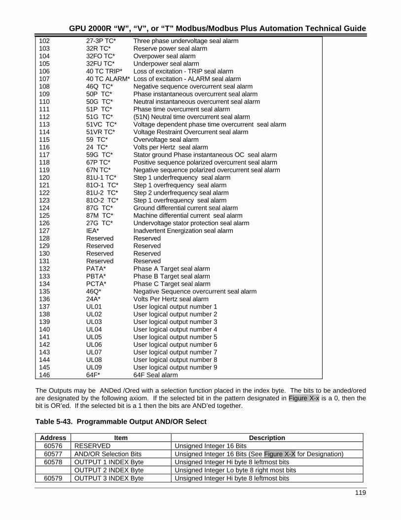
GPU 2000R “W”, “V”, or “T” Modbus/Modbus Plus Automation Technical Guide
119
102 27-3P TC* Three phase undervoltage seal alarm103 32R TC* Reserve power seal alarm104 32FO TC* Overpower seal alarm105 32FU TC* Underpower seal alarm106 40 TC TRIP* Loss of excitation - TRIP seal alarm107 40 TC ALARM* Loss of excitation - ALARM seal alarm108 46Q TC* Negative sequence overcurrent seal alarm109 50P TC* Phase instantaneous overcurrent seal alarm110 50G TC* Neutral instantaneous overcurrent seal alarm111 51P TC* Phase time overcurrent seal alarm112 51G TC* (51N) Neutral time overcurrent seal alarm113 51VC TC* Voltage dependent phase time overcurrent seal alarm114 51VR TC* Voltage Restraint Overcurrent seal alarm115 59 TC* Overvoltage seal alarm116 24 TC* Volts per Hertz seal alarm117 59G TC* Stator ground Phase instantaneous OC seal alarm118 67P TC* Positive sequence polarized overcurrent seal alarm119 67N TC* Negative sequence polarized overcurrent seal alarm120 81U-1 TC* Step 1 underfrequency seal alarm121 81O-1 TC* Step 1 overfrequency seal alarm122 81U-2 TC* Step 2 underfrequency seal alarm123 81O-2 TC* Step 1 overfrequency seal alarm124 87G TC* Ground differential current seal alarm125 87M TC* Machine differential current seal alarm126 27G TC* Undervoltage stator protection seal alarm127 IEA* Inadvertent Energization seal alarm128 Reserved Reserved129 Reserved Reserved130 Reserved Reserved131 Reserved Reserved132 PATA* Phase A Target seal alarm133 PBTA* Phase B Target seal alarm134 PCTA* Phase C Target seal alarm135 46Q* Negative Sequence overcurrent seal alarm136 24A* Volts Per Hertz seal alarm137 UL01 User logical output number 1138 UL02 User logical output number 2139 UL03 User logical output number 3140 UL04 User logical output number 4141 UL05 User logical output number 5142 UL06 User logical output number 6143 UL07 User logical output number 7144 UL08 User logical output number 8145 UL09 User logical output number 9146 64F* 64F Seal alarm
The Outputs may be ANDed /Ored with a selection function placed in the index byte. The bits to be anded/oredare designated by the following axiom. If the selected bit in the pattern designated in Figure X-x is a 0, then thebit is OR’ed. If the selected bit is a 1 then the bits are AND’ed together.
Table 5-43. Programmable Output AND/OR Select
Address Item Description60576 RESERVED Unsigned Integer 16 Bits60577 AND/OR Selection Bits Unsigned Integer 16 Bits (See Figure X-X for Designation)60578 OUTPUT 1 INDEX Byte Unsigned Integer Hi byte 8 leftmost bits
OUTPUT 2 INDEX Byte Unsigned Integer Lo byte 8 right most bits60579 OUTPUT 3 INDEX Byte Unsigned Integer Hi byte 8 leftmost bits
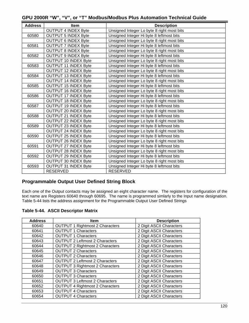
GPU 2000R “W”, “V”, or “T” Modbus/Modbus Plus Automation Technical Guide
120
Address Item DescriptionOUTPUT 4 INDEX Byte Unsigned Integer Lo byte 8 right most bits
60580 OUTPUT 5 INDEX Byte Unsigned Integer Hi byte 8 leftmost bitsOUTPUT 6 INDEX Byte Unsigned Integer Lo byte 8 right most bits
60581 OUTPUT 7 INDEX Byte Unsigned Integer Hi byte 8 leftmost bitsOUTPUT 8 INDEX Byte Unsigned Integer Lo byte 8 right most bits
60582 OUTPUT 9 INDEX Byte Unsigned Integer Hi byte 8 leftmost bitsOUTPUT 10 INDEX Byte Unsigned Integer Lo byte 8 right most bits
60583 OUTPUT 11 INDEX Byte Unsigned Integer Hi byte 8 leftmost bitsOUTPUT 12 INDEX Byte Unsigned Integer Lo byte 8 right most bits
60584 OUTPUT 13 INDEX Byte Unsigned Integer Hi byte 8 leftmost bitsOUTPUT 14 INDEX Byte Unsigned Integer Lo byte 8 right most bits
60585 OUTPUT 15 INDEX Byte Unsigned Integer Hi byte 8 leftmost bitsOUTPUT 16 INDEX Byte Unsigned Integer Lo byte 8 right most bits
60586 OUTPUT 17 INDEX Byte Unsigned Integer Hi byte 8 leftmost bitsOUTPUT 18 INDEX Byte Unsigned Integer Lo byte 8 right most bits
60587 OUTPUT 19 INDEX Byte Unsigned Integer Hi byte 8 leftmost bitsOUTPUT 20 INDEX Byte Unsigned Integer Lo byte 8 right most bits
60588 OUTPUT 21 INDEX Byte Unsigned Integer Hi byte 8 leftmost bitsOUTPUT 22 INDEX Byte Unsigned Integer Lo byte 8 right most bits
60589 OUTPUT 23 INDEX Byte Unsigned Integer Hi byte 8 leftmost bitsOUTPUT 24 INDEX Byte Unsigned Integer Lo byte 8 right most bits
60590 OUTPUT 25 INDEX Byte Unsigned Integer Hi byte 8 leftmost bitsOUTPUT 26 INDEX Byte Unsigned Integer Lo byte 8 right most bits
60591 OUTPUT 27 INDEX Byte Unsigned Integer Hi byte 8 leftmost bitsOUTPUT 28 INDEX Byte Unsigned Integer Lo byte 8 right most bits
60592 OUTPUT 29 INDEX Byte Unsigned Integer Hi byte 8 leftmost bitsOUTPUT 30 INDEX Byte Unsigned Integer Lo byte 8 right most bits
60593 OUTPUT 31 INDEX Byte Unsigned Integer Hi byte 8 leftmost bitsRESERVED RESERVED
Programmable Output User Defined String Block
Each one of the Output contacts may be assigned an eight character name. The registers for configuration of thetext name are Registers 60640 through 60695. The name is programmed simlarly to the Input name designation.Table 5-44 lists the address assignment for the Programmable Output User Defined Strings
Table 5-44. ASCII Descriptor Matrix
Address Item Description60640 OUTPUT 1 Rightmost 2 Characters 2 Digit ASCII Characters60641 OUTPUT 1 Characters 2 Digit ASCII Characters60642 OUTPUT 1 Characters 2 Digit ASCII Characters60643 OUTPUT 2 Leftmost 2 Characters 2 Digit ASCII Characters60644 OUTPUT 2 Rightmost 2 Characters 2 Digit ASCII Characters60645 OUTPUT 2 Characters 2 Digit ASCII Characters60646 OUTPUT 2 Characters 2 Digit ASCII Characters60647 OUTPUT 2 Leftmost 2 Characters 2 Digit ASCII Characters60648 OUTPUT 3 Rightmost 2 Characters 2 Digit ASCII Characters60649 OUTPUT 3 Characters 2 Digit ASCII Characters60650 OUTPUT 3 Characters 2 Digit ASCII Characters60651 OUTPUT 3 Leftmost 2 Characters 2 Digit ASCII Characters60652 OUTPUT 4 Rightmost 2 Characters 2 Digit ASCII Characters60653 OUTPUT 4 Characters 2 Digit ASCII Characters60654 OUTPUT 4 Characters 2 Digit ASCII Characters
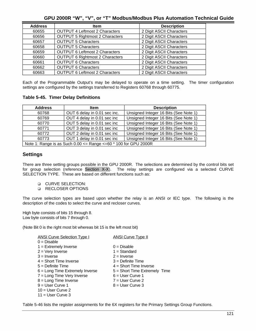
GPU 2000R “W”, “V”, or “T” Modbus/Modbus Plus Automation Technical Guide
121
Address Item Description60655 OUTPUT 4 Leftmost 2 Characters 2 Digit ASCII Characters60656 OUTPUT 5 Rightmost 2 Characters 2 Digit ASCII Characters60657 OUTPUT 5 Characters 2 Digit ASCII Characters60658 OUTPUT 5 Characters 2 Digit ASCII Characters60659 OUTPUT 6 Leftmost 2 Characters 2 Digit ASCII Characters60660 OUTPUT 6 Rightmost 2 Characters 2 Digit ASCII Characters60661 OUTPUT 6 Characters 2 Digit ASCII Characters60662 OUTPUT 6 Characters 2 Digit ASCII Characters60663 OUTPUT 6 Leftmost 2 Characters 2 Digit ASCII Characters
Each of the Programmable Output’s may be delayed to operate on a time setting. The timer configurationsettings are configured by the settings transferred to Registers 60768 through 60775.
Table 5-45. Timer Delay Definitions
Address Item Description60768 OUT 6 delay in 0.01 sec inc. Unsigned Integer 16 Bits (See Note 1)60769 OUT 4 delay in 0.01 sec inc Unsigned Integer 16 Bits (See Note 1)60770 OUT 5 delay in 0.01 sec inc Unsigned Integer 16 Bits (See Note 1)60771 OUT 3 delay in 0.01 sec inc Unsigned Integer 16 Bits (See Note 1)60772 OUT 2 delay in 0.01 sec inc Unsigned Integer 16 Bits (See Note 1)60773 OUT 1 delay in 0.01 sec inc Unsigned Integer 16 Bits (See Note 1)
Note 1: Range is as Such 0.00 <= Range <=60 * 100 for GPU 2000R
Settings
There are three setting groups possible in the GPU 2000R. The selections are determined by the control bits setfor group selection (reference Section X-X). The relay settings are configured via a selected CURVESELECTION TYPE. These are based on different functions such as:
CURVE SELECTION: RECLOSER OPTIONS
The curve selection types are based upon whether the relay is an ANSI or IEC type. The following is thedescription of the codes to select the curve and recloser curves.
High byte consists of bits 15 through 8.Low byte consists of bits 7 through 0.
(Note Bit 0 is the right most bit whereas bit 15 is the left most bit)
ANSI Curve Selection Type I ANSI Curve Type II0 = Disable1 = Extremely Inverse 0 = Disable2 = Very Inverse 1 = Standard3 = Inverse 2 = Inverse4 = Short Time Inverse 3 = Definite Time5 = Definite Time 4 = Short Time Inverse6 = Long Time Extremely Inverse 5 = Short Time Extremely Time7 = Long Time Very Inverse 6 = User Curve 18 = Long Time Inverse 7 = User Curve 29 = User Curve 1 8 = User Curve 310 = User Curve 211 = User Curve 3
Table 5-46 lists the register assignments for the 6X registers for the Primary Settings Group Functions.
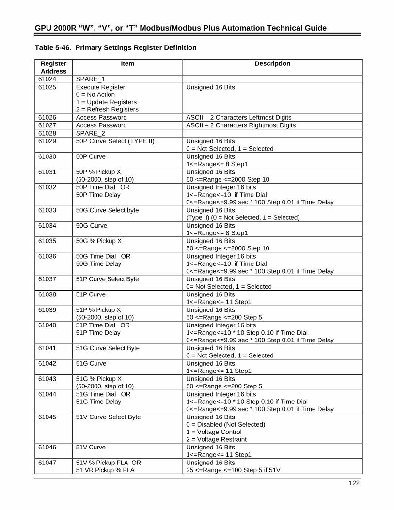
GPU 2000R “W”, “V”, or “T” Modbus/Modbus Plus Automation Technical Guide
122
Table 5-46. Primary Settings Register Definition
RegisterAddress
Item Description
61024 SPARE_161025 Execute Register
0 = No Action1 = Update Registers2 = Refresh Registers
Unsigned 16 Bits
61026 Access Password ASCII – 2 Characters Leftmost Digits61027 Access Password ASCII – 2 Characters Rightmost Digits61028 SPARE_261029 50P Curve Select (TYPE II) Unsigned 16 Bits
0 = Not Selected, 1 = Selected61030 50P Curve Unsigned 16 Bits
1<=Range<= 8 Step161031 50P % Pickup X
(50-2000, step of 10)Unsigned 16 Bits50 <=Range <=2000 Step 10
61032 50P Time Dial OR50P Time Delay
Unsigned Integer 16 bits1<=Range<=10 if Time Dial0<=Range<=9.99 sec * 100 Step 0.01 if Time Delay
61033 50G Curve Select byte Unsigned 16 Bits(Type II) (0 = Not Selected, 1 = Selected)
61034 50G Curve Unsigned 16 Bits1<=Range<= 8 Step1
61035 50G % Pickup X Unsigned 16 Bits50 <=Range <=2000 Step 10
61036 50G Time Dial OR50G Time Delay
Unsigned Integer 16 bits1<=Range<=10 if Time Dial0<=Range<=9.99 sec * 100 Step 0.01 if Time Delay
61037 51P Curve Select Byte Unsigned 16 Bits0= Not Selected, 1 = Selected
61038 51P Curve Unsigned 16 Bits1<=Range<= 11 Step1
61039 51P % Pickup X(50-2000, step of 10)
Unsigned 16 Bits50 <=Range <=200 Step 5
61040 51P Time Dial OR51P Time Delay
Unsigned Integer 16 bits1<=Range<=10 * 10 Step 0.10 if Time Dial0<=Range<=9.99 sec * 100 Step 0.01 if Time Delay
61041 51G Curve Select Byte Unsigned 16 Bits0 = Not Selected, 1 = Selected
61042 51G Curve Unsigned 16 Bits1<=Range<= 11 Step1
61043 51G % Pickup X(50-2000, step of 10)
Unsigned 16 Bits50 <=Range <=200 Step 5
61044 51G Time Dial OR51G Time Delay
Unsigned Integer 16 bits1<=Range<=10 * 10 Step 0.10 if Time Dial0<=Range<=9.99 sec * 100 Step 0.01 if Time Delay
61045 51V Curve Select Byte Unsigned 16 Bits0 = Disabled (Not Selected)1 = Voltage Control2 = Voltage Restraint
61046 51V Curve Unsigned 16 Bits1<=Range<= 11 Step1
61047 51V % Pickup FLA OR51 VR Pickup % FLA
Unsigned 16 Bits25 <=Range <=100 Step 5 if 51V
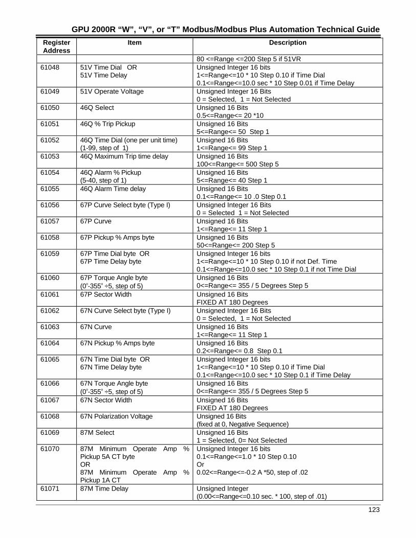
GPU 2000R “W”, “V”, or “T” Modbus/Modbus Plus Automation Technical Guide
123
RegisterAddress
Item Description
80 <=Range <=200 Step 5 if 51VR61048 51V Time Dial OR
51V Time DelayUnsigned Integer 16 bits1<=Range<=10 * 10 Step 0.10 if Time Dial0.1<=Range<=10.0 sec * 10 Step 0.01 if Time Delay
61049 51V Operate Voltage Unsigned Integer 16 Bits0 = Selected, 1 = Not Selected
61050 46Q Select Unsigned 16 Bits0.5<=Range<= 20 *10
61051 46Q % Trip Pickup Unsigned 16 Bits5<=Range<= 50 Step 1
61052 46Q Time Dial (one per unit time)(1-99, step of 1)
Unsigned 16 Bits1<=Range<= 99 Step 1
61053 46Q Maximum Trip time delay Unsigned 16 Bits100<=Range<= 500 Step 5
61054 46Q Alarm % Pickup(5-40, step of 1)
Unsigned 16 Bits5<=Range<= 40 Step 1
61055 46Q Alarm Time delay Unsigned 16 Bits0.1<=Range<= 10 .0 Step 0.1
61056 67P Curve Select byte (Type I) Unsigned Integer 16 Bits0 = Selected 1 = Not Selected
61057 67P Curve Unsigned 16 Bits1<=Range<= 11 Step 1
61058 67P Pickup % Amps byte Unsigned 16 Bits50<=Range<= 200 Step 5
61059 67P Time Dial byte OR67P Time Delay byte
Unsigned Integer 16 bits1<=Range<=10 * 10 Step 0.10 if not Def. Time0.1<=Range<=10.0 sec * 10 Step 0.1 if not Time Dial
61060 67P Torque Angle byte(0o-355o ÷5, step of 5)
Unsigned 16 Bits0<=Range<= 355 / 5 Degrees Step 5
61061 67P Sector Width Unsigned 16 BitsFIXED AT 180 Degrees
61062 67N Curve Select byte (Type I) Unsigned Integer 16 Bits0 = Selected, 1 = Not Selected
61063 67N Curve Unsigned 16 Bits1<=Range<= 11 Step 1
61064 67N Pickup % Amps byte Unsigned 16 Bits0.2<=Range<= 0.8 Step 0.1
61065 67N Time Dial byte OR67N Time Delay byte
Unsigned Integer 16 bits1<=Range<=10 * 10 Step 0.10 if Time Dial0.1<=Range<=10.0 sec * 10 Step 0.1 if Time Delay
61066 67N Torque Angle byte(0o-355o ÷5, step of 5)
Unsigned 16 Bits0<=Range<= 355 / 5 Degrees Step 5
61067 67N Sector Width Unsigned 16 BitsFIXED AT 180 Degrees
61068 67N Polarization Voltage Unsigned 16 Bits(fixed at 0, Negative Sequence)
61069 87M Select Unsigned 16 Bits1 = Selected, 0= Not Selected
61070 87M Minimum Operate Amp %Pickup 5A CT byteOR87M Minimum Operate Amp %Pickup 1A CT
Unsigned Integer 16 bits0.1<=Range<=1.0 * 10 Step 0.10Or0.02<=Range<=-0.2 A *50, step of .02
61071 87M Time Delay Unsigned Integer(0.00<=Range<=0.10 sec. * 100, step of .01)
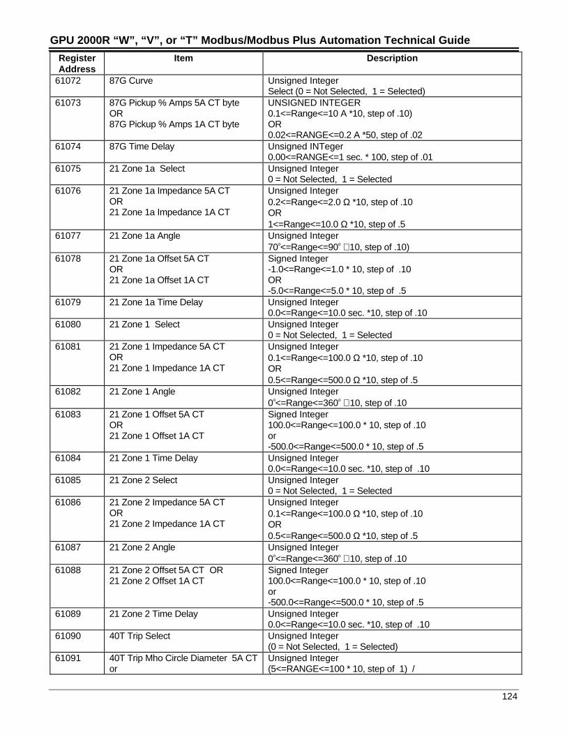
GPU 2000R “W”, “V”, or “T” Modbus/Modbus Plus Automation Technical Guide
124
RegisterAddress
Item Description
61072 87G Curve Unsigned IntegerSelect (0 = Not Selected, 1 = Selected)
61073 87G Pickup % Amps 5A CT byte OR87G Pickup % Amps 1A CT byte
UNSIGNED INTEGER0.1<=Range<=10 A *10, step of .10)OR0.02<=RANGE<=0.2 A *50, step of .02
61074 87G Time Delay Unsigned INTeger0.00<=RANGE<=1 sec. * 100, step of .01
61075 21 Zone 1a Select Unsigned Integer0 = Not Selected, 1 = Selected
61076 21 Zone 1a Impedance 5A CTOR21 Zone 1a Impedance 1A CT
Unsigned Integer0.2<=Range<=2.0 Ω *10, step of .10OR1<=Range<=10.0 Ω *10, step of .5
61077 21 Zone 1a Angle Unsigned Integer70o<=Range<=90o ∗ 10, step of .10)
61078 21 Zone 1a Offset 5A CTOR21 Zone 1a Offset 1A CT
Signed Integer-1.0<=Range<=1.0 * 10, step of .10OR-5.0<=Range<=5.0 * 10, step of .5
61079 21 Zone 1a Time Delay Unsigned Integer0.0<=Range<=10.0 sec. *10, step of .10
61080 21 Zone 1 Select Unsigned Integer0 = Not Selected, 1 = Selected
61081 21 Zone 1 Impedance 5A CTOR21 Zone 1 Impedance 1A CT
Unsigned Integer0.1<=Range<=100.0 Ω *10, step of .10OR0.5<=Range<=500.0 Ω *10, step of .5
61082 21 Zone 1 Angle Unsigned Integer0o<=Range<=360o ∗ 10, step of .10
61083 21 Zone 1 Offset 5A CTOR21 Zone 1 Offset 1A CT
Signed Integer100.0<=Range<=100.0 * 10, step of .10or-500.0<=Range<=500.0 * 10, step of .5
61084 21 Zone 1 Time Delay Unsigned Integer0.0<=Range<=10.0 sec. *10, step of .10
61085 21 Zone 2 Select Unsigned Integer0 = Not Selected, 1 = Selected
61086 21 Zone 2 Impedance 5A CTOR21 Zone 2 Impedance 1A CT
Unsigned Integer0.1<=Range<=100.0 Ω *10, step of .10OR0.5<=Range<=500.0 Ω *10, step of .5
61087 21 Zone 2 Angle Unsigned Integer0o<=Range<=360o ∗ 10, step of .10
61088 21 Zone 2 Offset 5A CT OR21 Zone 2 Offset 1A CT
Signed Integer100.0<=Range<=100.0 * 10, step of .10or-500.0<=Range<=500.0 * 10, step of .5
61089 21 Zone 2 Time Delay Unsigned Integer0.0<=Range<=10.0 sec. *10, step of .10
61090 40T Trip Select Unsigned Integer(0 = Not Selected, 1 = Selected)
61091 40T Trip Mho Circle Diameter 5A CTor
Unsigned Integer(5<=RANGE<=100 * 10, step of 1) /
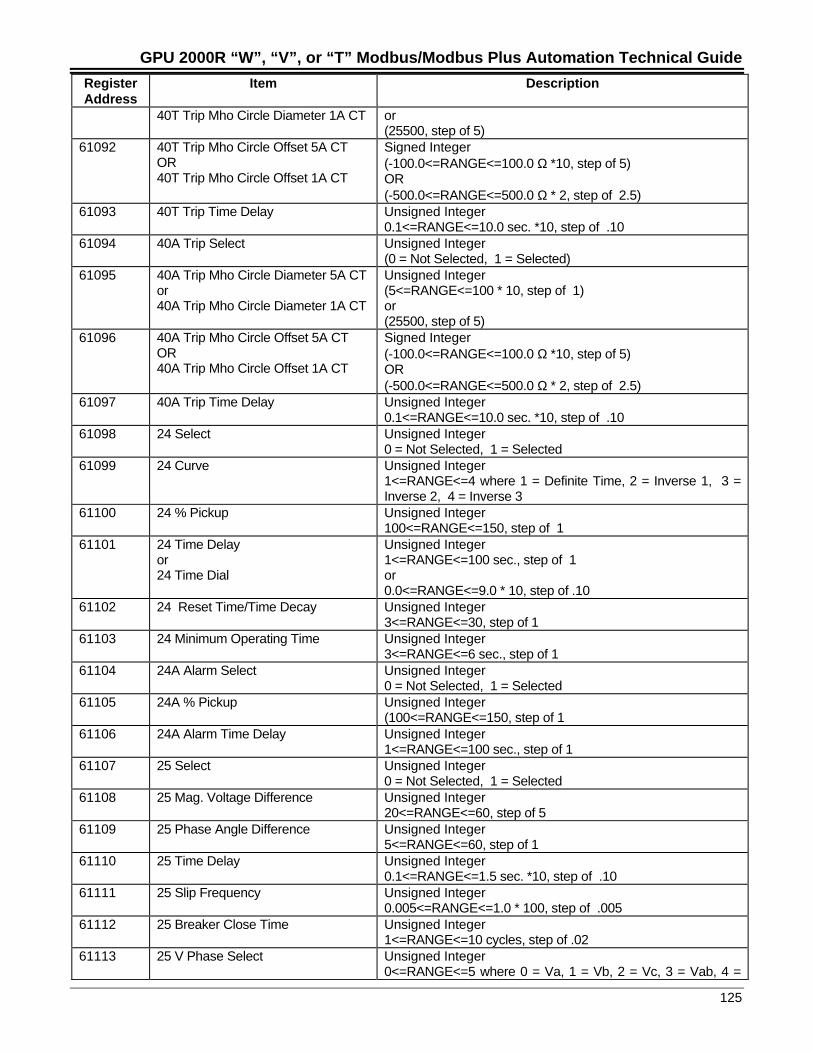
GPU 2000R “W”, “V”, or “T” Modbus/Modbus Plus Automation Technical Guide
125
RegisterAddress
Item Description
40T Trip Mho Circle Diameter 1A CT or(25500, step of 5)
61092 40T Trip Mho Circle Offset 5A CTOR40T Trip Mho Circle Offset 1A CT
Signed Integer(-100.0<=RANGE<=100.0 Ω *10, step of 5)OR(-500.0<=RANGE<=500.0 Ω * 2, step of 2.5)
61093 40T Trip Time Delay Unsigned Integer0.1<=RANGE<=10.0 sec. *10, step of .10
61094 40A Trip Select Unsigned Integer(0 = Not Selected, 1 = Selected)
61095 40A Trip Mho Circle Diameter 5A CTor40A Trip Mho Circle Diameter 1A CT
Unsigned Integer(5<=RANGE<=100 * 10, step of 1)or(25500, step of 5)
61096 40A Trip Mho Circle Offset 5A CTOR40A Trip Mho Circle Offset 1A CT
Signed Integer(-100.0<=RANGE<=100.0 Ω *10, step of 5)OR(-500.0<=RANGE<=500.0 Ω * 2, step of 2.5)
61097 40A Trip Time Delay Unsigned Integer0.1<=RANGE<=10.0 sec. *10, step of .10
61098 24 Select Unsigned Integer0 = Not Selected, 1 = Selected
61099 24 Curve Unsigned Integer1<=RANGE<=4 where 1 = Definite Time, 2 = Inverse 1, 3 =Inverse 2, 4 = Inverse 3
61100 24 % Pickup Unsigned Integer100<=RANGE<=150, step of 1
61101 24 Time Delayor24 Time Dial
Unsigned Integer1<=RANGE<=100 sec., step of 1or0.0<=RANGE<=9.0 * 10, step of .10
61102 24 Reset Time/Time Decay Unsigned Integer3<=RANGE<=30, step of 1
61103 24 Minimum Operating Time Unsigned Integer3<=RANGE<=6 sec., step of 1
61104 24A Alarm Select Unsigned Integer0 = Not Selected, 1 = Selected
61105 24A % Pickup Unsigned Integer(100<=RANGE<=150, step of 1
61106 24A Alarm Time Delay Unsigned Integer1<=RANGE<=100 sec., step of 1
61107 25 Select Unsigned Integer0 = Not Selected, 1 = Selected
61108 25 Mag. Voltage Difference Unsigned Integer20<=RANGE<=60, step of 5
61109 25 Phase Angle Difference Unsigned Integer5<=RANGE<=60, step of 1
61110 25 Time Delay Unsigned Integer0.1<=RANGE<=1.5 sec. *10, step of .10
61111 25 Slip Frequency Unsigned Integer0.005<=RANGE<=1.0 * 100, step of .005
61112 25 Breaker Close Time Unsigned Integer1<=RANGE<=10 cycles, step of .02
61113 25 V Phase Select Unsigned Integer0<=RANGE<=5 where 0 = Va, 1 = Vb, 2 = Vc, 3 = Vab, 4 =
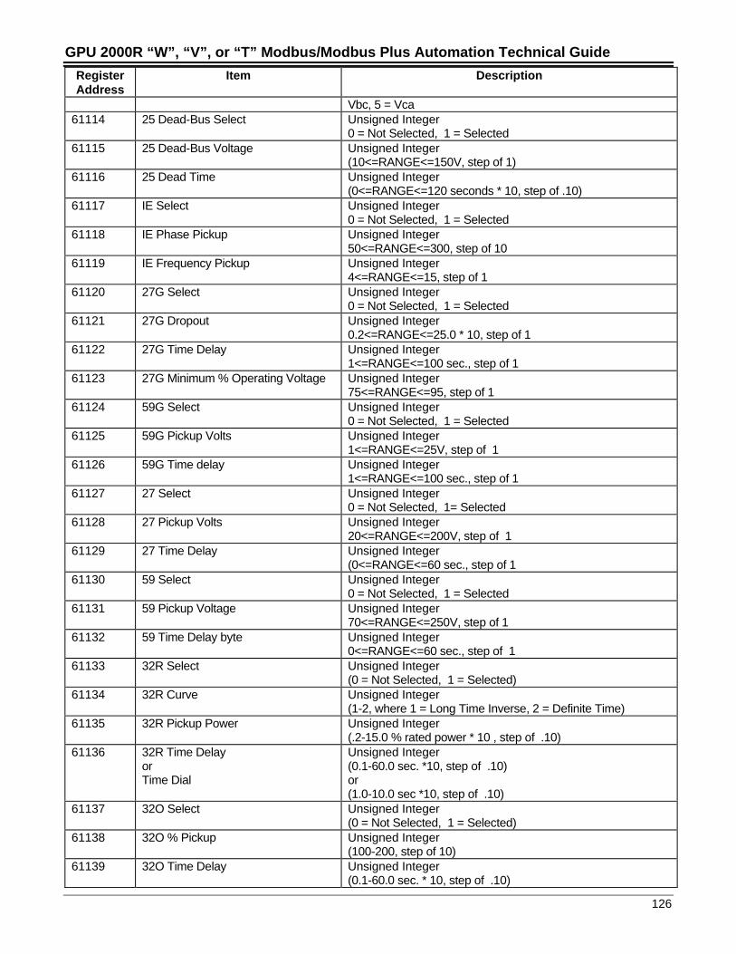
GPU 2000R “W”, “V”, or “T” Modbus/Modbus Plus Automation Technical Guide
126
RegisterAddress
Item Description
Vbc, 5 = Vca61114 25 Dead-Bus Select Unsigned Integer
0 = Not Selected, 1 = Selected61115 25 Dead-Bus Voltage Unsigned Integer
(10<=RANGE<=150V, step of 1)61116 25 Dead Time Unsigned Integer
(0<=RANGE<=120 seconds * 10, step of .10)61117 IE Select Unsigned Integer
0 = Not Selected, 1 = Selected61118 IE Phase Pickup Unsigned Integer
50<=RANGE<=300, step of 1061119 IE Frequency Pickup Unsigned Integer
4<=RANGE<=15, step of 161120 27G Select Unsigned Integer
0 = Not Selected, 1 = Selected61121 27G Dropout Unsigned Integer
0.2<=RANGE<=25.0 * 10, step of 161122 27G Time Delay Unsigned Integer
1<=RANGE<=100 sec., step of 161123 27G Minimum % Operating Voltage Unsigned Integer
75<=RANGE<=95, step of 161124 59G Select Unsigned Integer
0 = Not Selected, 1 = Selected61125 59G Pickup Volts Unsigned Integer
1<=RANGE<=25V, step of 161126 59G Time delay Unsigned Integer
1<=RANGE<=100 sec., step of 161127 27 Select Unsigned Integer
0 = Not Selected, 1= Selected61128 27 Pickup Volts Unsigned Integer
20<=RANGE<=200V, step of 161129 27 Time Delay Unsigned Integer
(0<=RANGE<=60 sec., step of 161130 59 Select Unsigned Integer
0 = Not Selected, 1 = Selected61131 59 Pickup Voltage Unsigned Integer
70<=RANGE<=250V, step of 161132 59 Time Delay byte Unsigned Integer
0<=RANGE<=60 sec., step of 161133 32R Select Unsigned Integer
(0 = Not Selected, 1 = Selected)61134 32R Curve Unsigned Integer
(1-2, where 1 = Long Time Inverse, 2 = Definite Time)61135 32R Pickup Power Unsigned Integer
(.2-15.0 % rated power * 10 , step of .10)61136 32R Time Delay
orTime Dial
Unsigned Integer(0.1-60.0 sec. *10, step of .10)or(1.0-10.0 sec *10, step of .10)
61137 32O Select Unsigned Integer(0 = Not Selected, 1 = Selected)
61138 32O % Pickup Unsigned Integer(100-200, step of 10)
61139 32O Time Delay Unsigned Integer(0.1-60.0 sec. * 10, step of .10)
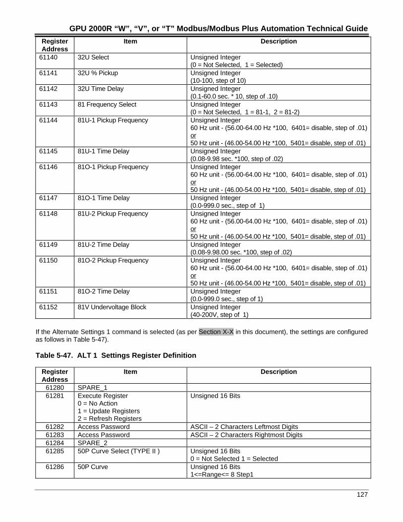
GPU 2000R “W”, “V”, or “T” Modbus/Modbus Plus Automation Technical Guide
127
RegisterAddress
Item Description
61140 32U Select Unsigned Integer(0 = Not Selected, 1 = Selected)
61141 32U % Pickup Unsigned Integer(10-100, step of 10)
61142 32U Time Delay Unsigned Integer(0.1-60.0 sec. * 10, step of .10)
61143 81 Frequency Select Unsigned Integer(0 = Not Selected, 1 = 81-1, 2 = 81-2)
61144 81U-1 Pickup Frequency Unsigned Integer60 Hz unit - (56.00-64.00 Hz *100, 6401= disable, step of .01)or50 Hz unit - (46.00-54.00 Hz *100, 5401= disable, step of .01)
61145 81U-1 Time Delay Unsigned Integer(0.08-9.98 sec. *100, step of .02)
61146 81O-1 Pickup Frequency Unsigned Integer60 Hz unit - (56.00-64.00 Hz *100, 6401= disable, step of .01)or50 Hz unit - (46.00-54.00 Hz *100, 5401= disable, step of .01)
61147 81O-1 Time Delay Unsigned Integer(0.0-999.0 sec., step of 1)
61148 81U-2 Pickup Frequency Unsigned Integer60 Hz unit - (56.00-64.00 Hz *100, 6401= disable, step of .01)or50 Hz unit - (46.00-54.00 Hz *100, 5401= disable, step of .01)
61149 81U-2 Time Delay Unsigned Integer(0.08-9.98.00 sec. *100, step of .02)
61150 81O-2 Pickup Frequency Unsigned Integer60 Hz unit - (56.00-64.00 Hz *100, 6401= disable, step of .01)or50 Hz unit - (46.00-54.00 Hz *100, 5401= disable, step of .01)
61151 81O-2 Time Delay Unsigned Integer(0.0-999.0 sec., step of 1)
61152 81V Undervoltage Block Unsigned Integer(40-200V, step of 1)
If the Alternate Settings 1 command is selected (as per Section X-X in this document), the settings are configuredas follows in Table 5-47).
Table 5-47. ALT 1 Settings Register Definition
RegisterAddress
Item Description
61280 SPARE_161281 Execute Register
0 = No Action1 = Update Registers2 = Refresh Registers
Unsigned 16 Bits
61282 Access Password ASCII – 2 Characters Leftmost Digits61283 Access Password ASCII – 2 Characters Rightmost Digits61284 SPARE_261285 50P Curve Select (TYPE II ) Unsigned 16 Bits
0 = Not Selected 1 = Selected61286 50P Curve Unsigned 16 Bits
1<=Range<= 8 Step1
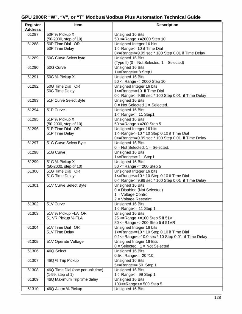
GPU 2000R “W”, “V”, or “T” Modbus/Modbus Plus Automation Technical Guide
128
RegisterAddress
Item Description
61287 50P % Pickup X(50-2000, step of 10)
Unsigned 16 Bits50 <=Range <=2000 Step 10
61288 50P Time Dial OR50P Time Delay
Unsigned Integer 16 bits1<=Range<=10 if Time Dial0<=Range<=9.99 sec * 100 Step 0.01 if Time Delay
61289 50G Curve Select byte Unsigned 16 Bits(Type II) (0 = Not Selected, 1 = Selected)
61290 50G Curve Unsigned 16 Bits1<=Range<= 8 Step1
61291 50G % Pickup X Unsigned 16 Bits50 <=Range <=2000 Step 10
61292 50G Time Dial OR50G Time Delay
Unsigned Integer 16 bits1<=Range<=10 if Time Dial0<=Range<=9.99 sec * 100 Step 0.01 if Time Delay
61293 51P Curve Select Byte Unsigned 16 Bits0 = Not Selected 1 = Selected.
61294 51P Curve Unsigned 16 Bits1<=Range<= 11 Step1
61295 51P % Pickup X(50-2000, step of 10)
Unsigned 16 Bits50 <=Range <=200 Step 5
61296 51P Time Dial OR51P Time Delay
Unsigned Integer 16 bits1<=Range<=10 * 10 Step 0.10 if Time Dial0<=Range<=9.99 sec * 100 Step 0.01 if Time Delay
61297 51G Curve Select Byte Unsigned 16 Bits0 = Not Selected, 1 = Selected.
61298 51G Curve Unsigned 16 Bits1<=Range<= 11 Step1
61299 51G % Pickup X(50-2000, step of 10)
Unsigned 16 Bits50 <=Range <=200 Step 5
61300 51G Time Dial OR51G Time Delay
Unsigned Integer 16 bits1<=Range<=10 * 10 Step 0.10 if Time Dial0<=Range<=9.99 sec * 100 Step 0.01 if Time Delay
61301 51V Curve Select Byte Unsigned 16 Bits0 = Disabled (Not Selected)1 = Voltage Control2 = Voltage Restraint
61302 51V Curve Unsigned 16 Bits1<=Range<= 11 Step 1
61303 51V % Pickup FLA OR51 VR Pickup % FLA
Unsigned 16 Bits25 <=Range <=100 Step 5 if 51V80 <=Range <=200 Step 5 if 51VR
61304 51V Time Dial OR51V Time Delay
Unsigned Integer 16 bits1<=Range<=10 * 10 Step 0.10 if Time Dial0.1<=Range<=10.0 sec * 10 Step 0.01 if Time Delay
61305 51V Operate Voltage Unsigned Integer 16 Bits0 = Selected, 1 = Not Selected
61306 46Q Select Unsigned 16 Bits0.5<=Range<= 20 *10
61307 46Q % Trip Pickup Unsigned 16 Bits5<=Range<= 50 Step 1
61308 46Q Time Dial (one per unit time)(1-99, step of 1)
Unsigned 16 Bits1<=Range<= 99 Step 1
61309 46Q Maximum Trip time delay Unsigned 16 Bits100<=Range<= 500 Step 5
61310 46Q Alarm % Pickup Unsigned 16 Bits
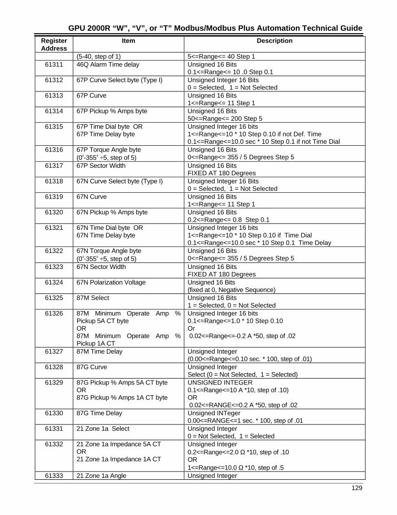
GPU 2000R “W”, “V”, or “T” Modbus/Modbus Plus Automation Technical Guide
129
RegisterAddress
Item Description
(5-40, step of 1) 5<=Range<= 40 Step 161311 46Q Alarm Time delay Unsigned 16 Bits
0.1<=Range<= 10 .0 Step 0.161312 67P Curve Select byte (Type I) Unsigned Integer 16 Bits
0 = Selected, 1 = Not Selected61313 67P Curve Unsigned 16 Bits
1<=Range<= 11 Step 161314 67P Pickup % Amps byte Unsigned 16 Bits
50<=Range<= 200 Step 561315 67P Time Dial byte OR
67P Time Delay byteUnsigned Integer 16 bits1<=Range<=10 * 10 Step 0.10 if not Def. Time0.1<=Range<=10.0 sec * 10 Step 0.1 if not Time Dial
61316 67P Torque Angle byte(0o-355o ÷5, step of 5)
Unsigned 16 Bits0<=Range<= 355 / 5 Degrees Step 5
61317 67P Sector Width Unsigned 16 BitsFIXED AT 180 Degrees
61318 67N Curve Select byte (Type I) Unsigned Integer 16 Bits0 = Selected, 1 = Not Selected
61319 67N Curve Unsigned 16 Bits1<=Range<= 11 Step 1
61320 67N Pickup % Amps byte Unsigned 16 Bits0.2<=Range<= 0.8 Step 0.1
61321 67N Time Dial byte OR67N Time Delay byte
Unsigned Integer 16 bits1<=Range<=10 * 10 Step 0.10 if Time Dial0.1<=Range<=10.0 sec * 10 Step 0.1 Time Delay
61322 67N Torque Angle byte(0o-355o ÷5, step of 5)
Unsigned 16 Bits0<=Range<= 355 / 5 Degrees Step 5
61323 67N Sector Width Unsigned 16 BitsFIXED AT 180 Degrees
61324 67N Polarization Voltage Unsigned 16 Bits(fixed at 0, Negative Sequence)
61325 87M Select Unsigned 16 Bits1 = Selected, 0 = Not Selected
61326 87M Minimum Operate Amp %Pickup 5A CT byteOR87M Minimum Operate Amp %Pickup 1A CT
Unsigned Integer 16 bits0.1<=Range<=1.0 * 10 Step 0.10Or 0.02<=Range<=-0.2 A *50, step of .02
61327 87M Time Delay Unsigned Integer(0.00<=Range<=0.10 sec. * 100, step of .01)
61328 87G Curve Unsigned IntegerSelect (0 = Not Selected, 1 = Selected)
61329 87G Pickup % Amps 5A CT byte OR87G Pickup % Amps 1A CT byte
UNSIGNED INTEGER0.1<=Range<=10 A *10, step of .10)OR 0.02<=RANGE<=0.2 A *50, step of .02
61330 87G Time Delay Unsigned INTeger0.00<=RANGE<=1 sec. * 100, step of .01
61331 21 Zone 1a Select Unsigned Integer0 = Not Selected, 1 = Selected
61332 21 Zone 1a Impedance 5A CTOR21 Zone 1a Impedance 1A CT
Unsigned Integer0.2<=Range<=2.0 Ω *10, step of .10OR1<=Range<=10.0 Ω *10, step of .5
61333 21 Zone 1a Angle Unsigned Integer
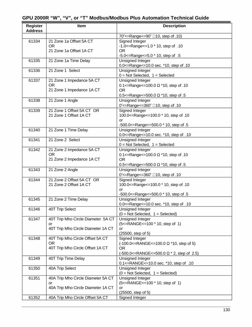
GPU 2000R “W”, “V”, or “T” Modbus/Modbus Plus Automation Technical Guide
130
RegisterAddress
Item Description
70o<=Range<=90o ∗ 10, step of .10)61334 21 Zone 1a Offset 5A CT
OR21 Zone 1a Offset 1A CT
Signed Integer-1.0<=Range<=1.0 * 10, step of .10OR-5.0<=Range<=5.0 * 10, step of .5
61335 21 Zone 1a Time Delay Unsigned Integer0.0<=Range<=10.0 sec. *10, step of .10
61336 21 Zone 1 Select Unsigned Integer0 = Not Selected, 1 = Selected
61337 21 Zone 1 Impedance 5A CTOR21 Zone 1 Impedance 1A CT
Unsigned Integer0.1<=Range<=100.0 Ω *10, step of .10OR0.5<=Range<=500.0 Ω *10, step of .5
61338 21 Zone 1 Angle Unsigned Integer0o<=Range<=360o ∗ 10, step of .10
61339 21 Zone 1 Offset 5A CT OR21 Zone 1 Offset 1A CT
Signed Integer100.0<=Range<=100.0 * 10, step of .10or-500.0<=Range<=500.0 * 10, step of .5
61340 21 Zone 1 Time Delay Unsigned Integer0.0<=Range<=10.0 sec. *10, step of .10
61341 21 Zone 2 Select Unsigned Integer0 = Not Selected, 1 = Selected
61342 21 Zone 2 Impedance 5A CTOR21 Zone 2 Impedance 1A CT
Unsigned Integer0.1<=Range<=100.0 Ω *10, step of .10OR0.5<=Range<=500.0 Ω *10, step of .5
61343 21 Zone 2 Angle Unsigned Integer0o<=Range<=360o ∗ 10, step of .10
61344 21 Zone 2 Offset 5A CT OR21 Zone 2 Offset 1A CT
Signed Integer100.0<=Range<=100.0 * 10, step of .10or-500.0<=Range<=500.0 * 10, step of .5
61345 21 Zone 2 Time Delay Unsigned Integer0.0<=Range<=10.0 sec. *10, step of .10
61346 40T Trip Select Unsigned Integer(0 = Not Selected, 1 = Selected)
61347 40T Trip Mho Circle Diameter 5A CTor40T Trip Mho Circle Diameter 1A CT
Unsigned Integer(5<=RANGE<=100 * 10, step of 1)or(25500, step of 5)
61348 40T Trip Mho Circle Offset 5A CTOR40T Trip Mho Circle Offset 1A CT
Signed Integer(-100.0<=RANGE<=100.0 Ω *10, step of 5)OR(-500.0<=RANGE<=500.0 Ω * 2, step of 2.5)
61349 40T Trip Time Delay Unsigned Integer0.1<=RANGE<=10.0 sec. *10, step of .10
61350 40A Trip Select Unsigned Integer(0 = Not Selected, 1 = Selected)
61351 40A Trip Mho Circle Diameter 5A CTor40A Trip Mho Circle Diameter 1A CT
Unsigned Integer(5<=RANGE<=100 * 10, step of 1)or(25500, step of 5)
61352 40A Trip Mho Circle Offset 5A CT Signed Integer
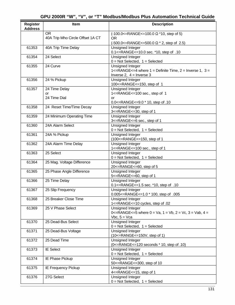
GPU 2000R “W”, “V”, or “T” Modbus/Modbus Plus Automation Technical Guide
131
RegisterAddress
Item Description
OR40A Trip Mho Circle Offset 1A CT
(-100.0<=RANGE<=100.0 Ω *10, step of 5)OR(-500.0<=RANGE<=500.0 Ω * 2, step of 2.5)
61353 40A Trip Time Delay Unsigned Integer0.1<=RANGE<=10.0 sec. *10, step of .10
61354 24 Select Unsigned Integer0 = Not Selected, 1 = Selected
61355 24 Curve Unsigned Integer1<=RANGE<=4 where 1 = Definite Time, 2 = Inverse 1, 3 =Inverse 2, 4 = Inverse 3
61356 24 % Pickup Unsigned Integer100<=RANGE<=150, step of 1
61357 24 Time Delayor24 Time Dial
Unsigned Integer1<=RANGE<=100 sec., step of 1or0.0<=RANGE<=9.0 * 10, step of .10
61358 24 Reset Time/Time Decay Unsigned Integer3<=RANGE<=30, step of 1
61359 24 Minimum Operating Time Unsigned Integer3<=RANGE<=6 sec., step of 1
61360 24A Alarm Select Unsigned Integer0 = Not Selected, 1 = Selected
61361 24A % Pickup Unsigned Integer(100<=RANGE<=150, step of 1
61362 24A Alarm Time Delay Unsigned Integer1<=RANGE<=100 sec., step of 1
61363 25 Select Unsigned Integer0 = Not Selected, 1 = Selected
61364 25 Mag. Voltage Difference Unsigned Integer20<=RANGE<=60, step of 5
61365 25 Phase Angle Difference Unsigned Integer5<=RANGE<=60, step of 1
61366 25 Time Delay Unsigned Integer0.1<=RANGE<=1.5 sec. *10, step of .10
61367 25 Slip Frequency Unsigned Integer0.005<=RANGE<=1.0 * 100, step of .005
61368 25 Breaker Close Time Unsigned Integer1<=RANGE<=10 cycles, step of .02
61369 25 V Phase Select Unsigned Integer0<=RANGE<=5 where 0 = Va, 1 = Vb, 2 = Vc, 3 = Vab, 4 =Vbc, 5 = Vca
61370 25 Dead-Bus Select Unsigned Integer0 = Not Selected, 1 = Selected
61371 25 Dead-Bus Voltage Unsigned Integer(10<=RANGE<=150V, step of 1)
61372 25 Dead Time Unsigned Integer(0<=RANGE<=120 seconds * 10, step of .10)
61373 IE Select Unsigned Integer0 = Not Selected, 1 = Selected
61374 IE Phase Pickup Unsigned Integer50<=RANGE<=300, step of 10
61375 IE Frequency Pickup Unsigned Integer4<=RANGE<=15, step of 1
61376 27G Select Unsigned Integer0 = Not Selected, 1 = Selected
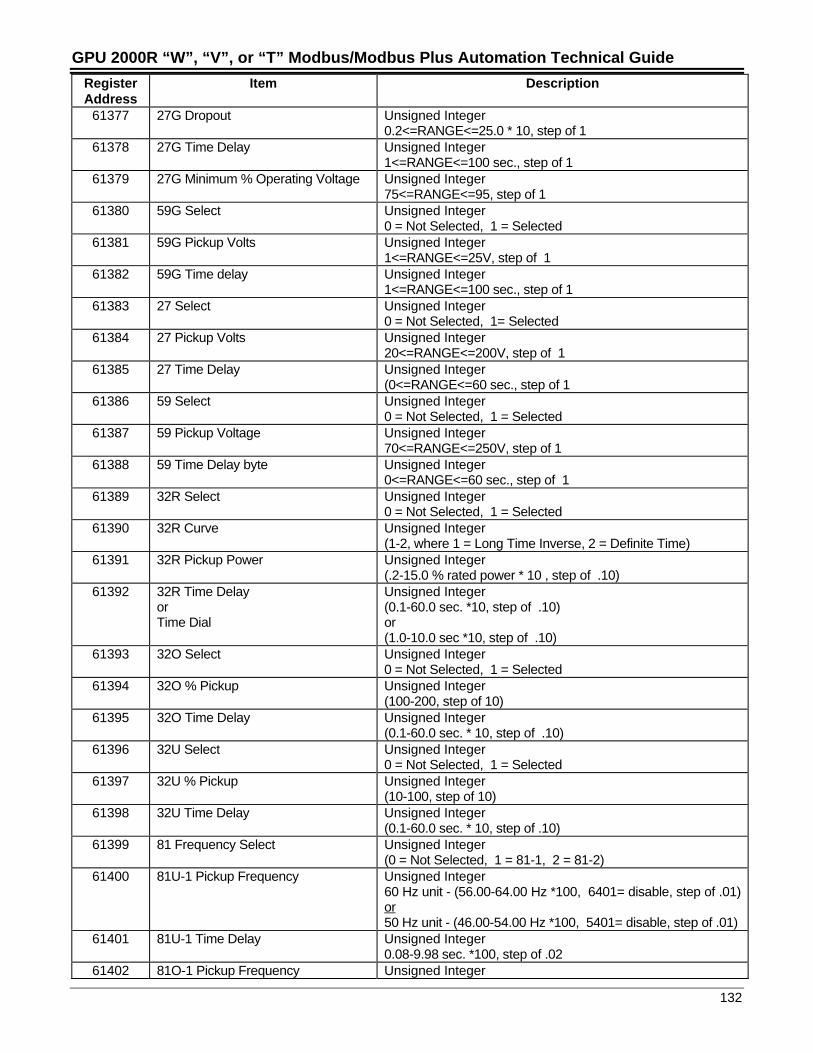
GPU 2000R “W”, “V”, or “T” Modbus/Modbus Plus Automation Technical Guide
132
RegisterAddress
Item Description
61377 27G Dropout Unsigned Integer0.2<=RANGE<=25.0 * 10, step of 1
61378 27G Time Delay Unsigned Integer1<=RANGE<=100 sec., step of 1
61379 27G Minimum % Operating Voltage Unsigned Integer75<=RANGE<=95, step of 1
61380 59G Select Unsigned Integer0 = Not Selected, 1 = Selected
61381 59G Pickup Volts Unsigned Integer1<=RANGE<=25V, step of 1
61382 59G Time delay Unsigned Integer1<=RANGE<=100 sec., step of 1
61383 27 Select Unsigned Integer0 = Not Selected, 1= Selected
61384 27 Pickup Volts Unsigned Integer20<=RANGE<=200V, step of 1
61385 27 Time Delay Unsigned Integer(0<=RANGE<=60 sec., step of 1
61386 59 Select Unsigned Integer0 = Not Selected, 1 = Selected
61387 59 Pickup Voltage Unsigned Integer70<=RANGE<=250V, step of 1
61388 59 Time Delay byte Unsigned Integer0<=RANGE<=60 sec., step of 1
61389 32R Select Unsigned Integer0 = Not Selected, 1 = Selected
61390 32R Curve Unsigned Integer(1-2, where 1 = Long Time Inverse, 2 = Definite Time)
61391 32R Pickup Power Unsigned Integer(.2-15.0 % rated power * 10 , step of .10)
61392 32R Time DelayorTime Dial
Unsigned Integer(0.1-60.0 sec. *10, step of .10)or(1.0-10.0 sec *10, step of .10)
61393 32O Select Unsigned Integer0 = Not Selected, 1 = Selected
61394 32O % Pickup Unsigned Integer(100-200, step of 10)
61395 32O Time Delay Unsigned Integer(0.1-60.0 sec. * 10, step of .10)
61396 32U Select Unsigned Integer0 = Not Selected, 1 = Selected
61397 32U % Pickup Unsigned Integer(10-100, step of 10)
61398 32U Time Delay Unsigned Integer(0.1-60.0 sec. * 10, step of .10)
61399 81 Frequency Select Unsigned Integer(0 = Not Selected, 1 = 81-1, 2 = 81-2)
61400 81U-1 Pickup Frequency Unsigned Integer60 Hz unit - (56.00-64.00 Hz *100, 6401= disable, step of .01)or50 Hz unit - (46.00-54.00 Hz *100, 5401= disable, step of .01)
61401 81U-1 Time Delay Unsigned Integer0.08-9.98 sec. *100, step of .02
61402 81O-1 Pickup Frequency Unsigned Integer
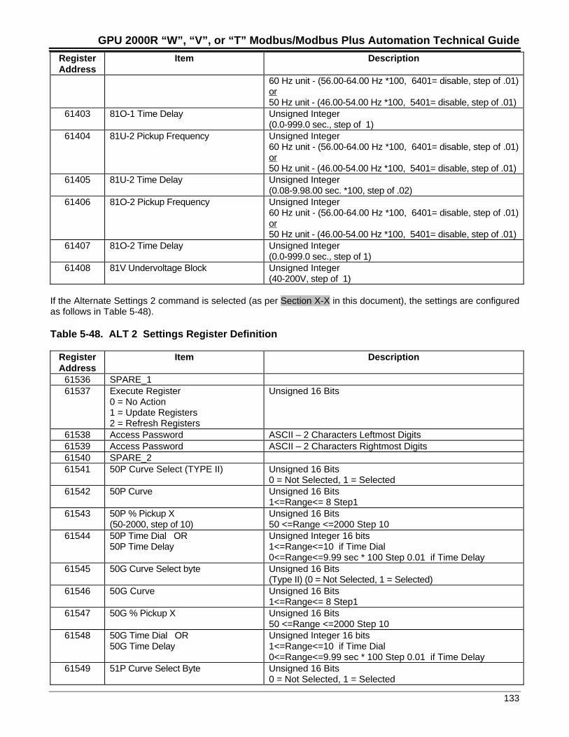
GPU 2000R “W”, “V”, or “T” Modbus/Modbus Plus Automation Technical Guide
133
RegisterAddress
Item Description
60 Hz unit - (56.00-64.00 Hz *100, 6401= disable, step of .01)or50 Hz unit - (46.00-54.00 Hz *100, 5401= disable, step of .01)
61403 81O-1 Time Delay Unsigned Integer(0.0-999.0 sec., step of 1)
61404 81U-2 Pickup Frequency Unsigned Integer60 Hz unit - (56.00-64.00 Hz *100, 6401= disable, step of .01)or50 Hz unit - (46.00-54.00 Hz *100, 5401= disable, step of .01)
61405 81U-2 Time Delay Unsigned Integer(0.08-9.98.00 sec. *100, step of .02)
61406 81O-2 Pickup Frequency Unsigned Integer60 Hz unit - (56.00-64.00 Hz *100, 6401= disable, step of .01)or50 Hz unit - (46.00-54.00 Hz *100, 5401= disable, step of .01)
61407 81O-2 Time Delay Unsigned Integer(0.0-999.0 sec., step of 1)
61408 81V Undervoltage Block Unsigned Integer(40-200V, step of 1)
If the Alternate Settings 2 command is selected (as per Section X-X in this document), the settings are configuredas follows in Table 5-48).
Table 5-48. ALT 2 Settings Register Definition
RegisterAddress
Item Description
61536 SPARE_161537 Execute Register
0 = No Action1 = Update Registers2 = Refresh Registers
Unsigned 16 Bits
61538 Access Password ASCII – 2 Characters Leftmost Digits61539 Access Password ASCII – 2 Characters Rightmost Digits61540 SPARE_261541 50P Curve Select (TYPE II) Unsigned 16 Bits
0 = Not Selected, 1 = Selected61542 50P Curve Unsigned 16 Bits
1<=Range<= 8 Step161543 50P % Pickup X
(50-2000, step of 10)Unsigned 16 Bits50 <=Range <=2000 Step 10
61544 50P Time Dial OR50P Time Delay
Unsigned Integer 16 bits1<=Range<=10 if Time Dial0<=Range<=9.99 sec * 100 Step 0.01 if Time Delay
61545 50G Curve Select byte Unsigned 16 Bits(Type II) (0 = Not Selected, 1 = Selected)
61546 50G Curve Unsigned 16 Bits1<=Range<= 8 Step1
61547 50G % Pickup X Unsigned 16 Bits50 <=Range <=2000 Step 10
61548 50G Time Dial OR50G Time Delay
Unsigned Integer 16 bits1<=Range<=10 if Time Dial0<=Range<=9.99 sec * 100 Step 0.01 if Time Delay
61549 51P Curve Select Byte Unsigned 16 Bits0 = Not Selected, 1 = Selected
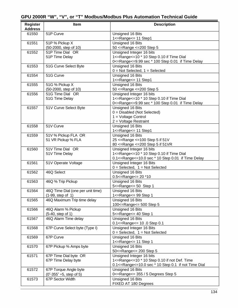
GPU 2000R “W”, “V”, or “T” Modbus/Modbus Plus Automation Technical Guide
134
RegisterAddress
Item Description
61550 51P Curve Unsigned 16 Bits1<=Range<= 11 Step1
61551 51P % Pickup X(50-2000, step of 10)
Unsigned 16 Bits50 <=Range <=200 Step 5
61552 51P Time Dial OR51P Time Delay
Unsigned Integer 16 bits1<=Range<=10 * 10 Step 0.10 if Time Dial0<=Range<=9.99 sec * 100 Step 0.01 if Time Delay
61553 51G Curve Select Byte Unsigned 16 Bits0 = Not Selected, 1 = Selected
61554 51G Curve Unsigned 16 Bits1<=Range<= 11 Step1
61555 51G % Pickup X(50-2000, step of 10)
Unsigned 16 Bits50 <=Range <=200 Step 5
61556 51G Time Dial OR51G Time Delay
Unsigned Integer 16 bits1<=Range<=10 * 10 Step 0.10 if Time Dial0<=Range<=9.99 sec * 100 Step 0.01 if Time Delay
61557 51V Curve Select Byte Unsigned 16 Bits0 = Disabled (Not Selected)1 = Voltage Control2 = Voltage Restraint
61558 51V Curve Unsigned 16 Bits1<=Range<= 11 Step1
61559 51V % Pickup FLA OR51 VR Pickup % FLA
Unsigned 16 Bits25 <=Range <=100 Step 5 if 51V80 <=Range <=200 Step 5 if 51VR
61560 51V Time Dial OR51V Time Delay
Unsigned Integer 16 bits1<=Range<=10 * 10 Step 0.10 if Time Dial0.1<=Range<=10.0 sec * 10 Step 0.01 if Time Delay
61561 51V Operate Voltage Unsigned Integer 16 Bits0 = Selected, 1 = Not Selected
61562 46Q Select Unsigned 16 Bits0.5<=Range<= 20 *10
61563 46Q % Trip Pickup Unsigned 16 Bits5<=Range<= 50 Step 1
61564 46Q Time Dial (one per unit time)(1-99, step of 1)
Unsigned 16 Bits1<=Range<= 99 Step 1
61565 46Q Maximum Trip time delay Unsigned 16 Bits100<=Range<= 500 Step 5
61566 46Q Alarm % Pickup(5-40, step of 1)
Unsigned 16 Bits5<=Range<= 40 Step 1
61567 46Q Alarm Time delay Unsigned 16 Bits0.1<=Range<= 10 .0 Step 0.1
61568 67P Curve Select byte (Type I) Unsigned Integer 16 Bits0 = Selected, 1 = Not Selected
61569 67P Curve Unsigned 16 Bits1<=Range<= 11 Step 1
61570 67P Pickup % Amps byte Unsigned 16 Bits50<=Range<= 200 Step 5
61571 67P Time Dial byte OR67P Time Delay byte
Unsigned Integer 16 bits1<=Range<=10 * 10 Step 0.10 if not Def. Time0.1<=Range<=10.0 sec * 10 Step 0.1 if not Time Dial
61572 67P Torque Angle byte(0o-355o ÷5, step of 5)
Unsigned 16 Bits0<=Range<= 355 / 5 Degrees Step 5
61573 67P Sector Width Unsigned 16 BitsFIXED AT 180 Degrees
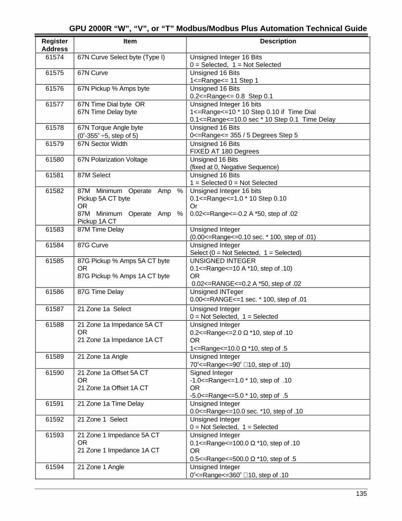
GPU 2000R “W”, “V”, or “T” Modbus/Modbus Plus Automation Technical Guide
135
RegisterAddress
Item Description
61574 67N Curve Select byte (Type I) Unsigned Integer 16 Bits0 = Selected, 1 = Not Selected
61575 67N Curve Unsigned 16 Bits1<=Range<= 11 Step 1
61576 67N Pickup % Amps byte Unsigned 16 Bits0.2<=Range<= 0.8 Step 0.1
61577 67N Time Dial byte OR67N Time Delay byte
Unsigned Integer 16 bits1<=Range<=10 * 10 Step 0.10 if Time Dial0.1<=Range<=10.0 sec * 10 Step 0.1 Time Delay
61578 67N Torque Angle byte(0o-355o ÷5, step of 5)
Unsigned 16 Bits0<=Range<= 355 / 5 Degrees Step 5
61579 67N Sector Width Unsigned 16 BitsFIXED AT 180 Degrees
61580 67N Polarization Voltage Unsigned 16 Bits(fixed at 0, Negative Sequence)
61581 87M Select Unsigned 16 Bits1 = Selected 0 = Not Selected
61582 87M Minimum Operate Amp %Pickup 5A CT byteOR87M Minimum Operate Amp %Pickup 1A CT
Unsigned Integer 16 bits0.1<=Range<=1.0 * 10 Step 0.10Or0.02<=Range<=-0.2 A *50, step of .02
61583 87M Time Delay Unsigned Integer(0.00<=Range<=0.10 sec. * 100, step of .01)
61584 87G Curve Unsigned IntegerSelect (0 = Not Selected, 1 = Selected)
61585 87G Pickup % Amps 5A CT byte OR87G Pickup % Amps 1A CT byte
UNSIGNED INTEGER0.1<=Range<=10 A *10, step of .10)OR 0.02<=RANGE<=0.2 A *50, step of .02
61586 87G Time Delay Unsigned INTeger0.00<=RANGE<=1 sec. * 100, step of .01
61587 21 Zone 1a Select Unsigned Integer0 = Not Selected, 1 = Selected
61588 21 Zone 1a Impedance 5A CTOR21 Zone 1a Impedance 1A CT
Unsigned Integer0.2<=Range<=2.0 Ω *10, step of .10OR1<=Range<=10.0 Ω *10, step of .5
61589 21 Zone 1a Angle Unsigned Integer70o<=Range<=90o ∗ 10, step of .10)
61590 21 Zone 1a Offset 5A CTOR21 Zone 1a Offset 1A CT
Signed Integer-1.0<=Range<=1.0 * 10, step of .10OR-5.0<=Range<=5.0 * 10, step of .5
61591 21 Zone 1a Time Delay Unsigned Integer0.0<=Range<=10.0 sec. *10, step of .10
61592 21 Zone 1 Select Unsigned Integer0 = Not Selected, 1 = Selected
61593 21 Zone 1 Impedance 5A CTOR21 Zone 1 Impedance 1A CT
Unsigned Integer0.1<=Range<=100.0 Ω *10, step of .10OR0.5<=Range<=500.0 Ω *10, step of .5
61594 21 Zone 1 Angle Unsigned Integer0o<=Range<=360o ∗ 10, step of .10
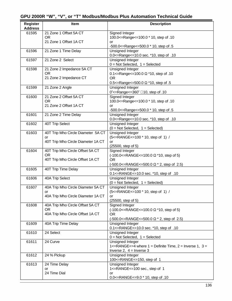
GPU 2000R “W”, “V”, or “T” Modbus/Modbus Plus Automation Technical Guide
136
RegisterAddress
Item Description
61595 21 Zone 1 Offset 5A CTOR21 Zone 1 Offset 1A CT
Signed Integer100.0<=Range<=100.0 * 10, step of .10or-500.0<=Range<=500.0 * 10, step of .5
61596 21 Zone 1 Time Delay Unsigned Integer0.0<=Range<=10.0 sec. *10, step of .10
61597 21 Zone 2 Select Unsigned Integer0 = Not Selected, 1 = Selected
61598 21 Zone 2 Impedance 5A CTOR21 Zone 2 Impedance CT
Unsigned Integer0.1<=Range<=100.0 Ω *10, step of .10OR0.5<=Range<=500.0 Ω *10, step of .5
61599 21 Zone 2 Angle Unsigned Integer0o<=Range<=360o ∗ 10, step of .10
61600 21 Zone 2 Offset 5A CTOR21 Zone 2 Offset 1A CT
Signed Integer100.0<=Range<=100.0 * 10, step of .10or-500.0<=Range<=500.0 * 10, step of .5
61601 21 Zone 2 Time Delay Unsigned Integer0.0<=Range<=10.0 sec. *10, step of .10
61602 40T Trip Select Unsigned Integer(0 = Not Selected, 1 = Selected)
61603 40T Trip Mho Circle Diameter 5A CTor40T Trip Mho Circle Diameter 1A CT
Unsigned Integer(5<=RANGE<=100 * 10, step of 1) /or(25500, step of 5)
61604 40T Trip Mho Circle Offset 5A CTOR40T Trip Mho Circle Offset 1A CT
Signed Integer(-100.0<=RANGE<=100.0 Ω *10, step of 5)OR(-500.0<=RANGE<=500.0 Ω * 2, step of 2.5)
61605 40T Trip Time Delay Unsigned Integer0.1<=RANGE<=10.0 sec. *10, step of .10
61606 40A Trip Select Unsigned Integer(0 = Not Selected, 1 = Selected)
61607 40A Trip Mho Circle Diameter 5A CTor40A Trip Mho Circle Diameter 1A CT
Unsigned Integer(5<=RANGE<=100 * 10, step of 1) /or(25500, step of 5)
61608 40A Trip Mho Circle Offset 5A CTOR40A Trip Mho Circle Offset 1A CT
Signed Integer(-100.0<=RANGE<=100.0 Ω *10, step of 5)OR(-500.0<=RANGE<=500.0 Ω * 2, step of 2.5)
61609 40A Trip Time Delay Unsigned Integer0.1<=RANGE<=10.0 sec. *10, step of .10
61610 24 Select Unsigned Integer0 = Not Selected, 1 = Selected
61611 24 Curve Unsigned Integer1<=RANGE<=4 where 1 = Definite Time, 2 = Inverse 1, 3 =Inverse 2, 4 = Inverse 3
61612 24 % Pickup Unsigned Integer100<=RANGE<=150, step of 1
61613 24 Time Delayor24 Time Dial
Unsigned Integer1<=RANGE<=100 sec., step of 1or0.0<=RANGE<=9.0 * 10, step of .10
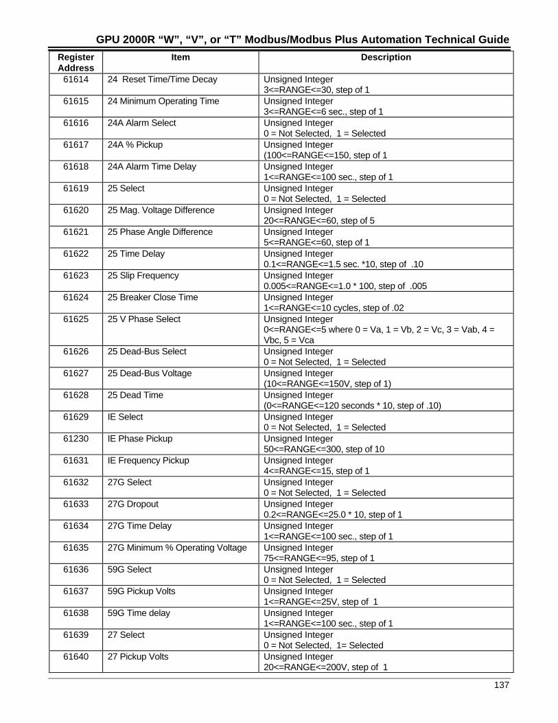
GPU 2000R “W”, “V”, or “T” Modbus/Modbus Plus Automation Technical Guide
137
RegisterAddress
Item Description
61614 24 Reset Time/Time Decay Unsigned Integer3<=RANGE<=30, step of 1
61615 24 Minimum Operating Time Unsigned Integer3<=RANGE<=6 sec., step of 1
61616 24A Alarm Select Unsigned Integer0 = Not Selected, 1 = Selected
61617 24A % Pickup Unsigned Integer(100<=RANGE<=150, step of 1
61618 24A Alarm Time Delay Unsigned Integer1<=RANGE<=100 sec., step of 1
61619 25 Select Unsigned Integer0 = Not Selected, 1 = Selected
61620 25 Mag. Voltage Difference Unsigned Integer20<=RANGE<=60, step of 5
61621 25 Phase Angle Difference Unsigned Integer5<=RANGE<=60, step of 1
61622 25 Time Delay Unsigned Integer0.1<=RANGE<=1.5 sec. *10, step of .10
61623 25 Slip Frequency Unsigned Integer0.005<=RANGE<=1.0 * 100, step of .005
61624 25 Breaker Close Time Unsigned Integer1<=RANGE<=10 cycles, step of .02
61625 25 V Phase Select Unsigned Integer0<=RANGE<=5 where 0 = Va, 1 = Vb, 2 = Vc, 3 = Vab, 4 =Vbc, 5 = Vca
61626 25 Dead-Bus Select Unsigned Integer0 = Not Selected, 1 = Selected
61627 25 Dead-Bus Voltage Unsigned Integer(10<=RANGE<=150V, step of 1)
61628 25 Dead Time Unsigned Integer(0<=RANGE<=120 seconds * 10, step of .10)
61629 IE Select Unsigned Integer0 = Not Selected, 1 = Selected
61230 IE Phase Pickup Unsigned Integer50<=RANGE<=300, step of 10
61631 IE Frequency Pickup Unsigned Integer4<=RANGE<=15, step of 1
61632 27G Select Unsigned Integer0 = Not Selected, 1 = Selected
61633 27G Dropout Unsigned Integer0.2<=RANGE<=25.0 * 10, step of 1
61634 27G Time Delay Unsigned Integer1<=RANGE<=100 sec., step of 1
61635 27G Minimum % Operating Voltage Unsigned Integer75<=RANGE<=95, step of 1
61636 59G Select Unsigned Integer0 = Not Selected, 1 = Selected
61637 59G Pickup Volts Unsigned Integer1<=RANGE<=25V, step of 1
61638 59G Time delay Unsigned Integer1<=RANGE<=100 sec., step of 1
61639 27 Select Unsigned Integer0 = Not Selected, 1= Selected
61640 27 Pickup Volts Unsigned Integer20<=RANGE<=200V, step of 1
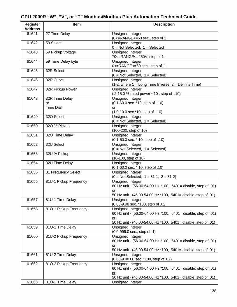
GPU 2000R “W”, “V”, or “T” Modbus/Modbus Plus Automation Technical Guide
138
RegisterAddress
Item Description
61641 27 Time Delay Unsigned Integer(0<=RANGE<=60 sec., step of 1
61642 59 Select Unsigned Integer0 = Not Selected, 1 = Selected
61643 59 Pickup Voltage Unsigned Integer70<=RANGE<=250V, step of 1
61644 59 Time Delay byte Unsigned Integer0<=RANGE<=60 sec., step of 1
61645 32R Select Unsigned Integer(0 = Not Selected, 1 = Selected)
61646 32R Curve Unsigned Integer(1-2, where 1 = Long Time Inverse, 2 = Definite Time)
61647 32R Pickup Power Unsigned Integer(.2-15.0 % rated power * 10 , step of .10)
61648 32R Time DelayorTime Dial
Unsigned Integer(0.1-60.0 sec. *10, step of .10)or(1.0-10.0 sec *10, step of .10)
61649 32O Select Unsigned Integer(0 = Not Selected, 1 = Selected)
61650 32O % Pickup Unsigned Integer(100-200, step of 10)
61651 32O Time Delay Unsigned Integer(0.1-60.0 sec. * 10, step of .10)
61652 32U Select Unsigned Integer(0 = Not Selected, 1 = Selected)
61653 32U % Pickup Unsigned Integer(10-100, step of 10)
61654 32U Time Delay Unsigned Integer(0.1-60.0 sec. * 10, step of .10)
61655 81 Frequency Select Unsigned Integer(0 = Not Selected, 1 = 81-1, 2 = 81-2)
61656 81U-1 Pickup Frequency Unsigned Integer60 Hz unit - (56.00-64.00 Hz *100, 6401= disable, step of .01)or50 Hz unit - (46.00-54.00 Hz *100, 5401= disable, step of .01)
61657 81U-1 Time Delay Unsigned Integer(0.08-9.98 sec. *100, step of .02
61658 81O-1 Pickup Frequency Unsigned Integer60 Hz unit - (56.00-64.00 Hz *100, 6401= disable, step of .01)or50 Hz unit - (46.00-54.00 Hz *100, 5401= disable, step of .01)
61659 81O-1 Time Delay Unsigned Integer(0.0-999.0 sec., step of 1)
61660 81U-2 Pickup Frequency Unsigned Integer60 Hz unit - (56.00-64.00 Hz *100, 6401= disable, step of .01)or50 Hz unit - (46.00-54.00 Hz *100, 5401= disable, step of .01)
61661 81U-2 Time Delay Unsigned Integer(0.08-9.98.00 sec. *100, step of .02)
61662 81O-2 Pickup Frequency Unsigned Integer60 Hz unit - (56.00-64.00 Hz *100, 6401= disable, step of .01)or50 Hz unit - (46.00-54.00 Hz *100, 5401= disable, step of .01)
61663 81O-2 Time Delay Unsigned Integer
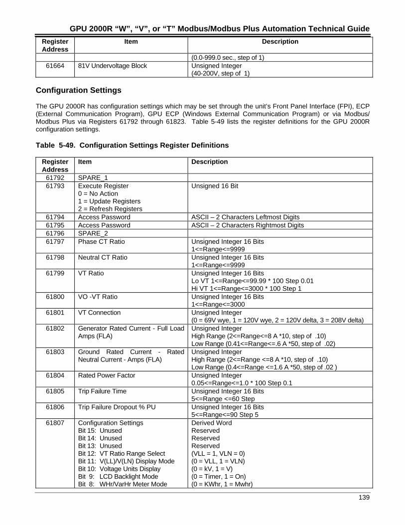
GPU 2000R “W”, “V”, or “T” Modbus/Modbus Plus Automation Technical Guide
139
RegisterAddress
Item Description
(0.0-999.0 sec., step of 1)61664 81V Undervoltage Block Unsigned Integer
(40-200V, step of 1)
Configuration Settings
The GPU 2000R has configuration settings which may be set through the unit’s Front Panel Interface (FPI), ECP(External Communication Program), GPU ECP (Windows External Communication Program) or via Modbus/Modbus Plus via Registers 61792 through 61823. Table 5-49 lists the register definitions for the GPU 2000Rconfiguration settings.
Table 5-49. Configuration Settings Register Definitions
RegisterAddress
Item Description
61792 SPARE_161793 Execute Register
0 = No Action1 = Update Registers2 = Refresh Registers
Unsigned 16 Bit
61794 Access Password ASCII – 2 Characters Leftmost Digits61795 Access Password ASCII – 2 Characters Rightmost Digits61796 SPARE_261797 Phase CT Ratio Unsigned Integer 16 Bits
1<=Range<=999961798 Neutral CT Ratio Unsigned Integer 16 Bits
1<=Range<=999961799 VT Ratio Unsigned Integer 16 Bits
Lo VT 1<=Range<=99.99 * 100 Step 0.01Hi VT 1<=Range<=3000 * 100 Step 1
61800 VO -VT Ratio Unsigned Integer 16 Bits1<=Range<=3000
61801 VT Connection Unsigned Integer(0 = 69V wye, 1 = 120V wye, 2 = 120V delta, 3 = 208V delta)
61802 Generator Rated Current - Full LoadAmps (FLA)
Unsigned IntegerHigh Range (2<=Range<=8 A *10, step of .10)Low Range (0.41<=Range<=.6 A *50, step of .02)
61803 Ground Rated Current - RatedNeutral Current - Amps (FLA)
Unsigned IntegerHigh Range (2<=Range <=8 A *10, step of .10)Low Range (0.4<=Range <=1.6 A *50, step of .02 )
61804 Rated Power Factor Unsigned Integer0.05<=Range<=1.0 * 100 Step 0.1
61805 Trip Failure Time Unsigned Integer 16 Bits5<=Range <=60 Step
61806 Trip Failure Dropout % PU Unsigned Integer 16 Bits5<=Range<=90 Step 5
61807 Configuration SettingsBit 15: UnusedBit 14: UnusedBit 13: UnusedBit 12: VT Ratio Range SelectBit 11: V(LL)/V(LN) Display ModeBit 10: Voltage Units DisplayBit 9: LCD Backlight ModeBit 8: WHr/VarHr Meter Mode
Derived WordReservedReservedReserved(VLL = 1, VLN = 0)(0 = VLL, 1 = VLN)(0 = kV, 1 = V)(0 = Timer, 1 = On)(0 = KWhr, 1 = Mwhr)
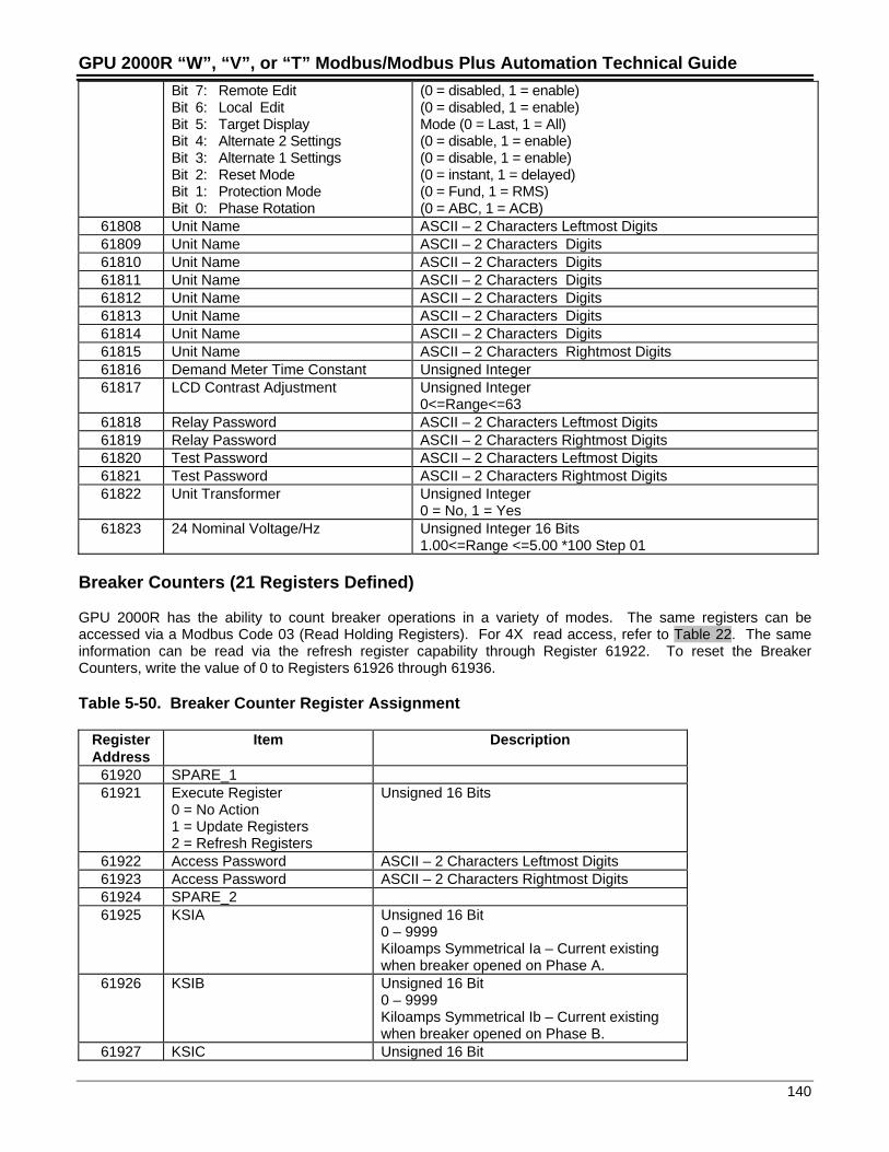
GPU 2000R “W”, “V”, or “T” Modbus/Modbus Plus Automation Technical Guide
140
Bit 7: Remote EditBit 6: Local EditBit 5: Target DisplayBit 4: Alternate 2 SettingsBit 3: Alternate 1 SettingsBit 2: Reset ModeBit 1: Protection ModeBit 0: Phase Rotation
(0 = disabled, 1 = enable)(0 = disabled, 1 = enable)Mode (0 = Last, 1 = All)(0 = disable, 1 = enable)(0 = disable, 1 = enable)(0 = instant, 1 = delayed)(0 = Fund, 1 = RMS)(0 = ABC, 1 = ACB)
61808 Unit Name ASCII – 2 Characters Leftmost Digits61809 Unit Name ASCII – 2 Characters Digits61810 Unit Name ASCII – 2 Characters Digits61811 Unit Name ASCII – 2 Characters Digits61812 Unit Name ASCII – 2 Characters Digits61813 Unit Name ASCII – 2 Characters Digits61814 Unit Name ASCII – 2 Characters Digits61815 Unit Name ASCII – 2 Characters Rightmost Digits61816 Demand Meter Time Constant Unsigned Integer61817 LCD Contrast Adjustment Unsigned Integer
0<=Range<=6361818 Relay Password ASCII – 2 Characters Leftmost Digits61819 Relay Password ASCII – 2 Characters Rightmost Digits61820 Test Password ASCII – 2 Characters Leftmost Digits61821 Test Password ASCII – 2 Characters Rightmost Digits61822 Unit Transformer Unsigned Integer
0 = No, 1 = Yes61823 24 Nominal Voltage/Hz Unsigned Integer 16 Bits
1.00<=Range <=5.00 *100 Step 01
Breaker Counters (21 Registers Defined)
GPU 2000R has the ability to count breaker operations in a variety of modes. The same registers can beaccessed via a Modbus Code 03 (Read Holding Registers). For 4X read access, refer to Table 22. The sameinformation can be read via the refresh register capability through Register 61922. To reset the BreakerCounters, write the value of 0 to Registers 61926 through 61936.
Table 5-50. Breaker Counter Register Assignment
RegisterAddress
Item Description
61920 SPARE_161921 Execute Register
0 = No Action1 = Update Registers2 = Refresh Registers
Unsigned 16 Bits
61922 Access Password ASCII – 2 Characters Leftmost Digits61923 Access Password ASCII – 2 Characters Rightmost Digits61924 SPARE_261925 KSIA Unsigned 16 Bit
0 – 9999Kiloamps Symmetrical Ia – Current existingwhen breaker opened on Phase A.
61926 KSIB Unsigned 16 Bit0 – 9999Kiloamps Symmetrical Ib – Current existingwhen breaker opened on Phase B.
61927 KSIC Unsigned 16 Bit
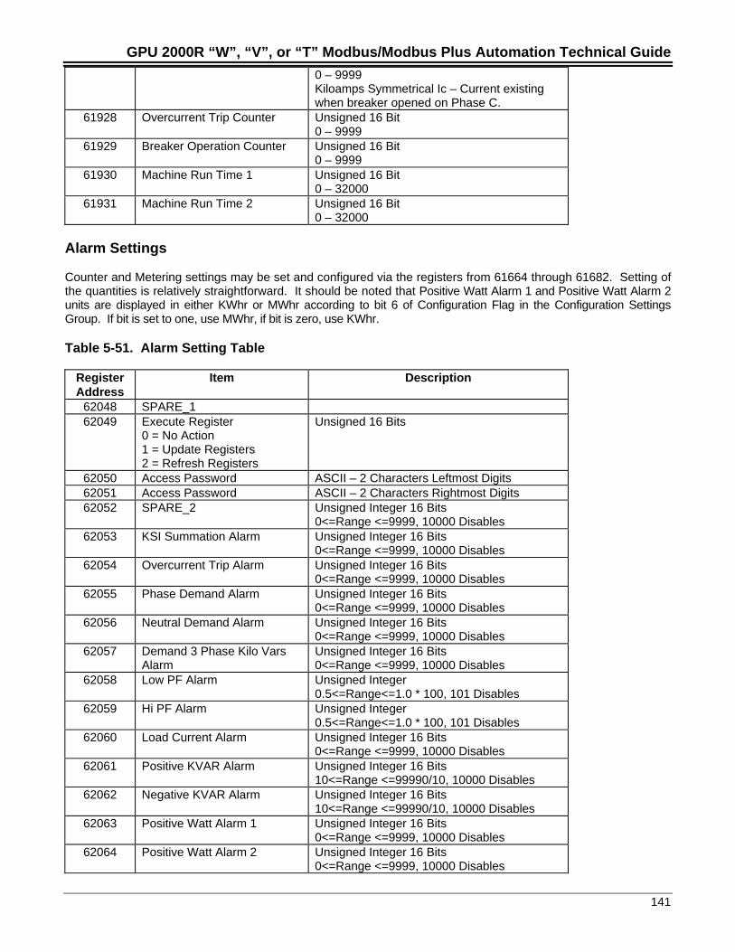
GPU 2000R “W”, “V”, or “T” Modbus/Modbus Plus Automation Technical Guide
141
0 – 9999Kiloamps Symmetrical Ic – Current existingwhen breaker opened on Phase C.
61928 Overcurrent Trip Counter Unsigned 16 Bit0 – 9999
61929 Breaker Operation Counter Unsigned 16 Bit0 – 9999
61930 Machine Run Time 1 Unsigned 16 Bit0 – 32000
61931 Machine Run Time 2 Unsigned 16 Bit0 – 32000
Alarm Settings
Counter and Metering settings may be set and configured via the registers from 61664 through 61682. Setting ofthe quantities is relatively straightforward. It should be noted that Positive Watt Alarm 1 and Positive Watt Alarm 2units are displayed in either KWhr or MWhr according to bit 6 of Configuration Flag in the Configuration SettingsGroup. If bit is set to one, use MWhr, if bit is zero, use KWhr.
Table 5-51. Alarm Setting Table
RegisterAddress
Item Description
62048 SPARE_162049 Execute Register
0 = No Action1 = Update Registers2 = Refresh Registers
Unsigned 16 Bits
62050 Access Password ASCII – 2 Characters Leftmost Digits62051 Access Password ASCII – 2 Characters Rightmost Digits62052 SPARE_2 Unsigned Integer 16 Bits
0<=Range <=9999, 10000 Disables62053 KSI Summation Alarm Unsigned Integer 16 Bits
0<=Range <=9999, 10000 Disables62054 Overcurrent Trip Alarm Unsigned Integer 16 Bits
0<=Range <=9999, 10000 Disables62055 Phase Demand Alarm Unsigned Integer 16 Bits
0<=Range <=9999, 10000 Disables62056 Neutral Demand Alarm Unsigned Integer 16 Bits
0<=Range <=9999, 10000 Disables62057 Demand 3 Phase Kilo Vars
AlarmUnsigned Integer 16 Bits0<=Range <=9999, 10000 Disables
62058 Low PF Alarm Unsigned Integer0.5<=Range<=1.0 * 100, 101 Disables
62059 Hi PF Alarm Unsigned Integer0.5<=Range<=1.0 * 100, 101 Disables
62060 Load Current Alarm Unsigned Integer 16 Bits0<=Range <=9999, 10000 Disables
62061 Positive KVAR Alarm Unsigned Integer 16 Bits10<=Range <=99990/10, 10000 Disables
62062 Negative KVAR Alarm Unsigned Integer 16 Bits10<=Range <=99990/10, 10000 Disables
62063 Positive Watt Alarm 1 Unsigned Integer 16 Bits0<=Range <=9999, 10000 Disables
62064 Positive Watt Alarm 2 Unsigned Integer 16 Bits0<=Range <=9999, 10000 Disables
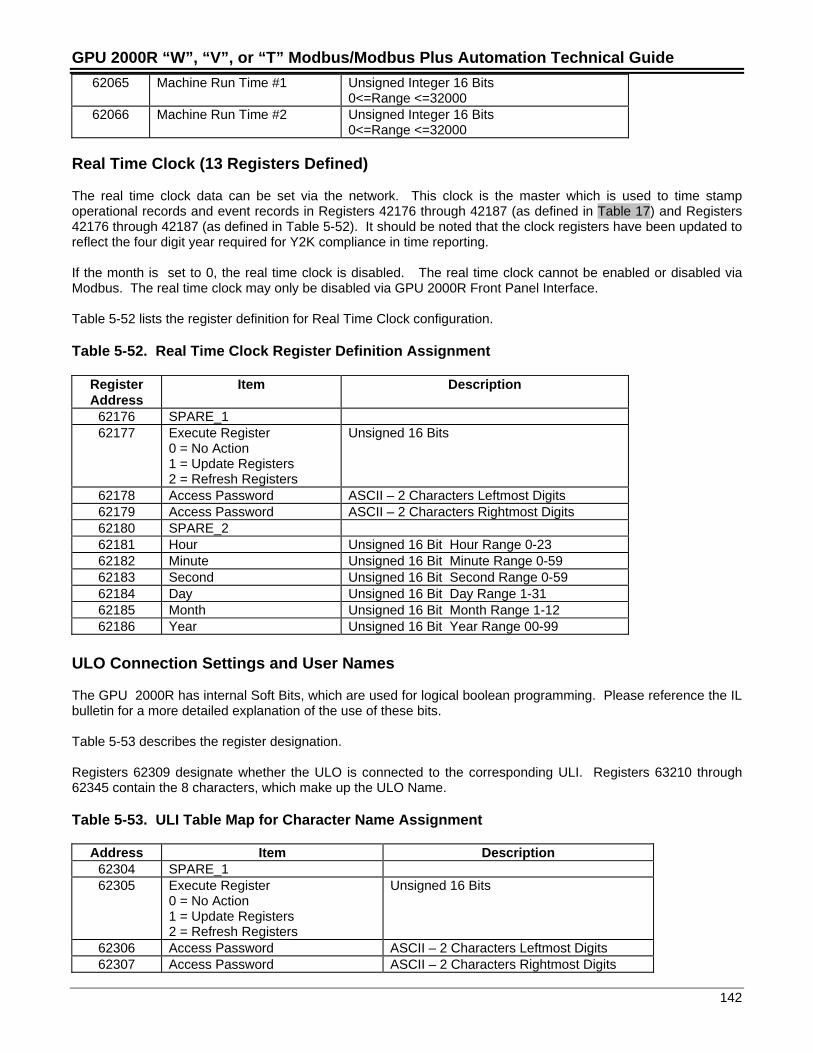
GPU 2000R “W”, “V”, or “T” Modbus/Modbus Plus Automation Technical Guide
142
62065 Machine Run Time #1 Unsigned Integer 16 Bits0<=Range <=32000
62066 Machine Run Time #2 Unsigned Integer 16 Bits0<=Range <=32000
Real Time Clock (13 Registers Defined)
The real time clock data can be set via the network. This clock is the master which is used to time stampoperational records and event records in Registers 42176 through 42187 (as defined in Table 17) and Registers42176 through 42187 (as defined in Table 5-52). It should be noted that the clock registers have been updated toreflect the four digit year required for Y2K compliance in time reporting.
If the month is set to 0, the real time clock is disabled. The real time clock cannot be enabled or disabled viaModbus. The real time clock may only be disabled via GPU 2000R Front Panel Interface.
Table 5-52 lists the register definition for Real Time Clock configuration.
Table 5-52. Real Time Clock Register Definition Assignment
RegisterAddress
Item Description
62176 SPARE_162177 Execute Register
0 = No Action1 = Update Registers2 = Refresh Registers
Unsigned 16 Bits
62178 Access Password ASCII – 2 Characters Leftmost Digits62179 Access Password ASCII – 2 Characters Rightmost Digits62180 SPARE_262181 Hour Unsigned 16 Bit Hour Range 0-2362182 Minute Unsigned 16 Bit Minute Range 0-5962183 Second Unsigned 16 Bit Second Range 0-5962184 Day Unsigned 16 Bit Day Range 1-3162185 Month Unsigned 16 Bit Month Range 1-1262186 Year Unsigned 16 Bit Year Range 00-99
ULO Connection Settings and User Names
The GPU 2000R has internal Soft Bits, which are used for logical boolean programming. Please reference the ILbulletin for a more detailed explanation of the use of these bits.
Table 5-53 describes the register designation.
Registers 62309 designate whether the ULO is connected to the corresponding ULI. Registers 63210 through62345 contain the 8 characters, which make up the ULO Name.
Table 5-53. ULI Table Map for Character Name Assignment
Address Item Description62304 SPARE_162305 Execute Register
0 = No Action1 = Update Registers2 = Refresh Registers
Unsigned 16 Bits
62306 Access Password ASCII – 2 Characters Leftmost Digits62307 Access Password ASCII – 2 Characters Rightmost Digits
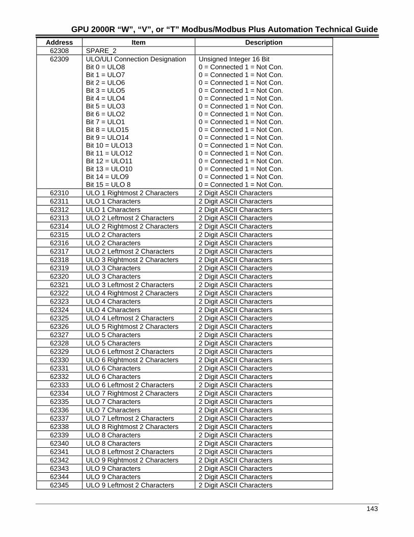
GPU 2000R “W”, “V”, or “T” Modbus/Modbus Plus Automation Technical Guide
143
Address Item Description62308 SPARE_262309 ULO/ULI Connection Designation
Bit 0 = ULO8Bit 1 = ULO7Bit 2 = ULO6Bit 3 = ULO5Bit 4 = ULO4Bit 5 = ULO3Bit 6 = ULO2Bit 7 = ULO1Bit 8 = ULO15Bit 9 = ULO14Bit 10 = ULO13Bit 11 = ULO12Bit 12 = ULO11Bit 13 = ULO10Bit 14 = ULO9Bit 15 = ULO 8
Unsigned Integer 16 Bit0 = Connected 1 = Not Con.0 = Connected 1 = Not Con.0 = Connected 1 = Not Con.0 = Connected 1 = Not Con.0 = Connected 1 = Not Con.0 = Connected 1 = Not Con.0 = Connected 1 = Not Con.0 = Connected 1 = Not Con.0 = Connected 1 = Not Con.0 = Connected 1 = Not Con.0 = Connected 1 = Not Con.0 = Connected 1 = Not Con.0 = Connected 1 = Not Con.0 = Connected 1 = Not Con.0 = Connected 1 = Not Con.0 = Connected 1 = Not Con.
62310 ULO 1 Rightmost 2 Characters 2 Digit ASCII Characters62311 ULO 1 Characters 2 Digit ASCII Characters62312 ULO 1 Characters 2 Digit ASCII Characters62313 ULO 2 Leftmost 2 Characters 2 Digit ASCII Characters62314 ULO 2 Rightmost 2 Characters 2 Digit ASCII Characters62315 ULO 2 Characters 2 Digit ASCII Characters62316 ULO 2 Characters 2 Digit ASCII Characters62317 ULO 2 Leftmost 2 Characters 2 Digit ASCII Characters62318 ULO 3 Rightmost 2 Characters 2 Digit ASCII Characters62319 ULO 3 Characters 2 Digit ASCII Characters62320 ULO 3 Characters 2 Digit ASCII Characters62321 ULO 3 Leftmost 2 Characters 2 Digit ASCII Characters62322 ULO 4 Rightmost 2 Characters 2 Digit ASCII Characters62323 ULO 4 Characters 2 Digit ASCII Characters62324 ULO 4 Characters 2 Digit ASCII Characters62325 ULO 4 Leftmost 2 Characters 2 Digit ASCII Characters62326 ULO 5 Rightmost 2 Characters 2 Digit ASCII Characters62327 ULO 5 Characters 2 Digit ASCII Characters62328 ULO 5 Characters 2 Digit ASCII Characters62329 ULO 6 Leftmost 2 Characters 2 Digit ASCII Characters62330 ULO 6 Rightmost 2 Characters 2 Digit ASCII Characters62331 ULO 6 Characters 2 Digit ASCII Characters62332 ULO 6 Characters 2 Digit ASCII Characters62333 ULO 6 Leftmost 2 Characters 2 Digit ASCII Characters62334 ULO 7 Rightmost 2 Characters 2 Digit ASCII Characters62335 ULO 7 Characters 2 Digit ASCII Characters62336 ULO 7 Characters 2 Digit ASCII Characters62337 ULO 7 Leftmost 2 Characters 2 Digit ASCII Characters62338 ULO 8 Rightmost 2 Characters 2 Digit ASCII Characters62339 ULO 8 Characters 2 Digit ASCII Characters62340 ULO 8 Characters 2 Digit ASCII Characters62341 ULO 8 Leftmost 2 Characters 2 Digit ASCII Characters62342 ULO 9 Rightmost 2 Characters 2 Digit ASCII Characters62343 ULO 9 Characters 2 Digit ASCII Characters62344 ULO 9 Characters 2 Digit ASCII Characters62345 ULO 9 Leftmost 2 Characters 2 Digit ASCII Characters
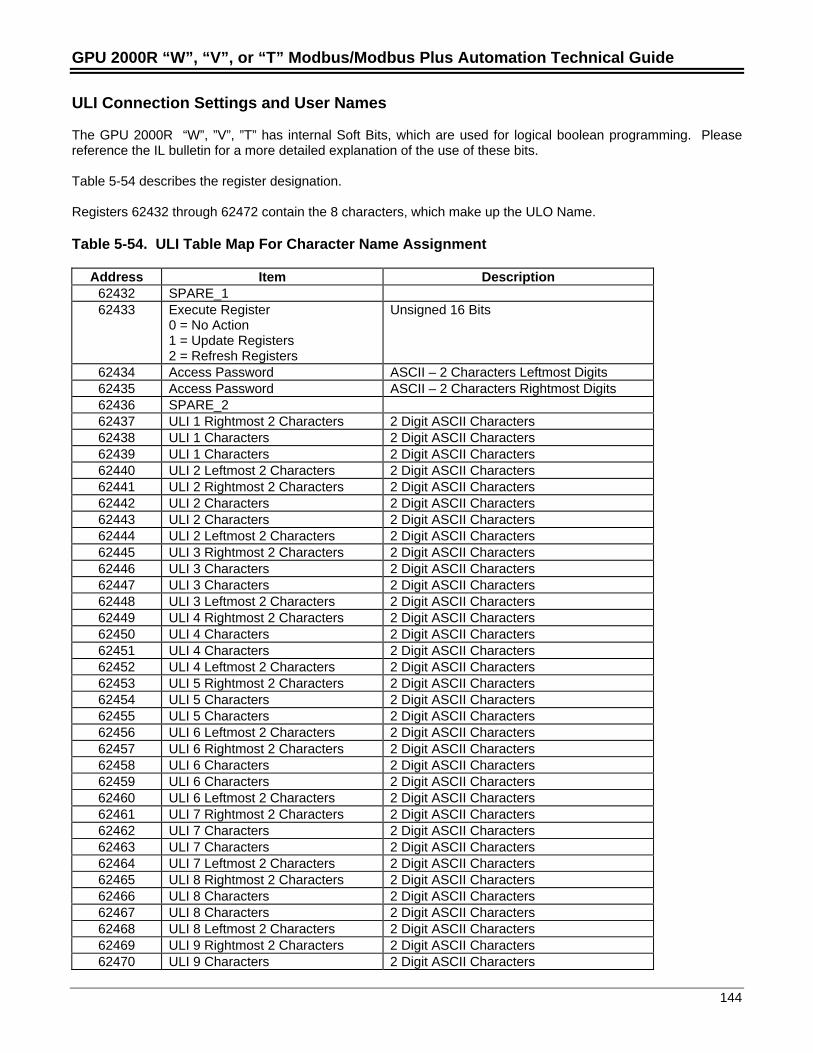
GPU 2000R “W”, “V”, or “T” Modbus/Modbus Plus Automation Technical Guide
144
ULI Connection Settings and User Names
The GPU 2000R “W”, ”V”, ”T” has internal Soft Bits, which are used for logical boolean programming. Pleasereference the IL bulletin for a more detailed explanation of the use of these bits.
Table 5-54 describes the register designation.
Registers 62432 through 62472 contain the 8 characters, which make up the ULO Name.
Table 5-54. ULI Table Map For Character Name Assignment
Address Item Description62432 SPARE_162433 Execute Register
0 = No Action1 = Update Registers2 = Refresh Registers
Unsigned 16 Bits
62434 Access Password ASCII – 2 Characters Leftmost Digits62435 Access Password ASCII – 2 Characters Rightmost Digits62436 SPARE_262437 ULI 1 Rightmost 2 Characters 2 Digit ASCII Characters62438 ULI 1 Characters 2 Digit ASCII Characters62439 ULI 1 Characters 2 Digit ASCII Characters62440 ULI 2 Leftmost 2 Characters 2 Digit ASCII Characters62441 ULI 2 Rightmost 2 Characters 2 Digit ASCII Characters62442 ULI 2 Characters 2 Digit ASCII Characters62443 ULI 2 Characters 2 Digit ASCII Characters62444 ULI 2 Leftmost 2 Characters 2 Digit ASCII Characters62445 ULI 3 Rightmost 2 Characters 2 Digit ASCII Characters62446 ULI 3 Characters 2 Digit ASCII Characters62447 ULI 3 Characters 2 Digit ASCII Characters62448 ULI 3 Leftmost 2 Characters 2 Digit ASCII Characters62449 ULI 4 Rightmost 2 Characters 2 Digit ASCII Characters62450 ULI 4 Characters 2 Digit ASCII Characters62451 ULI 4 Characters 2 Digit ASCII Characters62452 ULI 4 Leftmost 2 Characters 2 Digit ASCII Characters62453 ULI 5 Rightmost 2 Characters 2 Digit ASCII Characters62454 ULI 5 Characters 2 Digit ASCII Characters62455 ULI 5 Characters 2 Digit ASCII Characters62456 ULI 6 Leftmost 2 Characters 2 Digit ASCII Characters62457 ULI 6 Rightmost 2 Characters 2 Digit ASCII Characters62458 ULI 6 Characters 2 Digit ASCII Characters62459 ULI 6 Characters 2 Digit ASCII Characters62460 ULI 6 Leftmost 2 Characters 2 Digit ASCII Characters62461 ULI 7 Rightmost 2 Characters 2 Digit ASCII Characters62462 ULI 7 Characters 2 Digit ASCII Characters62463 ULI 7 Characters 2 Digit ASCII Characters62464 ULI 7 Leftmost 2 Characters 2 Digit ASCII Characters62465 ULI 8 Rightmost 2 Characters 2 Digit ASCII Characters62466 ULI 8 Characters 2 Digit ASCII Characters62467 ULI 8 Characters 2 Digit ASCII Characters62468 ULI 8 Leftmost 2 Characters 2 Digit ASCII Characters62469 ULI 9 Rightmost 2 Characters 2 Digit ASCII Characters62470 ULI 9 Characters 2 Digit ASCII Characters
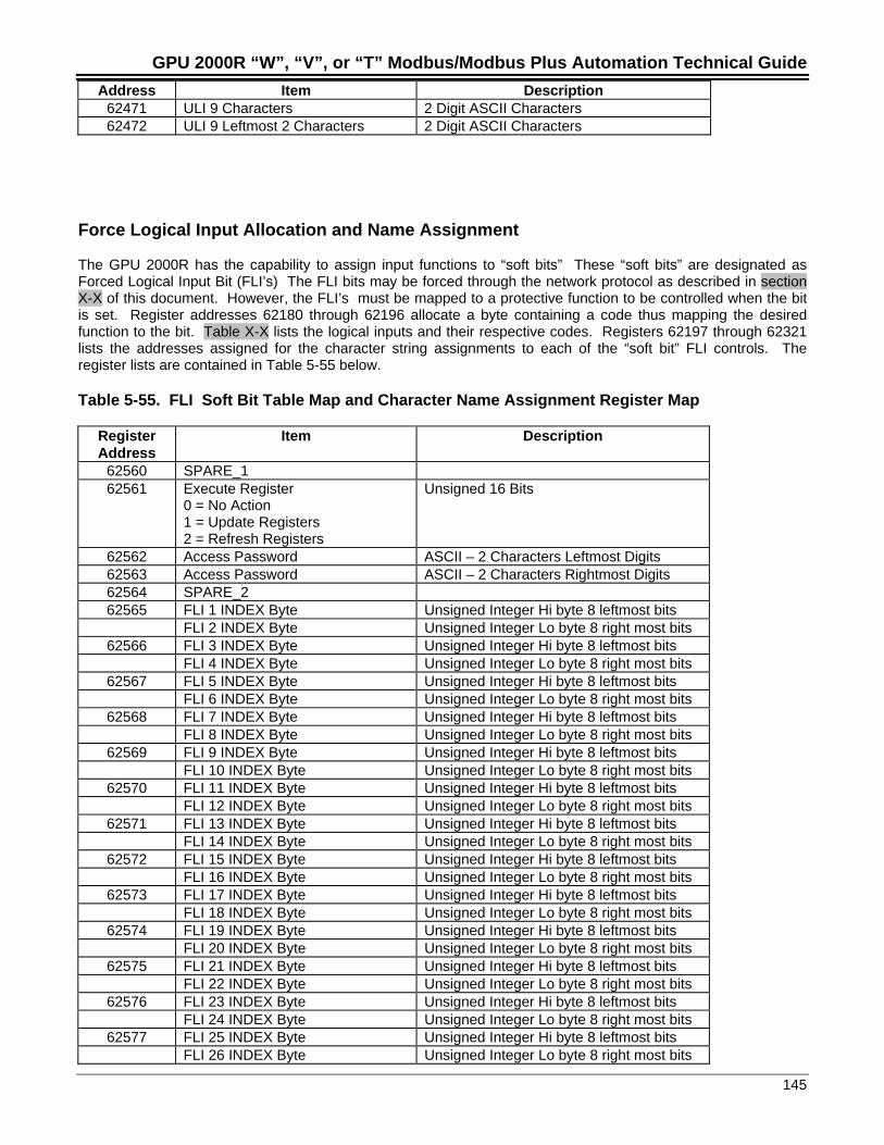
GPU 2000R “W”, “V”, or “T” Modbus/Modbus Plus Automation Technical Guide
145
Address Item Description62471 ULI 9 Characters 2 Digit ASCII Characters62472 ULI 9 Leftmost 2 Characters 2 Digit ASCII Characters
Force Logical Input Allocation and Name Assignment
The GPU 2000R has the capability to assign input functions to “soft bits” These “soft bits” are designated asForced Logical Input Bit (FLI’s) The FLI bits may be forced through the network protocol as described in sectionX-X of this document. However, the FLI’s must be mapped to a protective function to be controlled when the bitis set. Register addresses 62180 through 62196 allocate a byte containing a code thus mapping the desiredfunction to the bit. Table X-X lists the logical inputs and their respective codes. Registers 62197 through 62321lists the addresses assigned for the character string assignments to each of the “soft bit” FLI controls. Theregister lists are contained in Table 5-55 below.
Table 5-55. FLI Soft Bit Table Map and Character Name Assignment Register Map
RegisterAddress
Item Description
62560 SPARE_162561 Execute Register
0 = No Action1 = Update Registers2 = Refresh Registers
Unsigned 16 Bits
62562 Access Password ASCII – 2 Characters Leftmost Digits62563 Access Password ASCII – 2 Characters Rightmost Digits62564 SPARE_262565 FLI 1 INDEX Byte Unsigned Integer Hi byte 8 leftmost bits
FLI 2 INDEX Byte Unsigned Integer Lo byte 8 right most bits62566 FLI 3 INDEX Byte Unsigned Integer Hi byte 8 leftmost bits
FLI 4 INDEX Byte Unsigned Integer Lo byte 8 right most bits62567 FLI 5 INDEX Byte Unsigned Integer Hi byte 8 leftmost bits
FLI 6 INDEX Byte Unsigned Integer Lo byte 8 right most bits62568 FLI 7 INDEX Byte Unsigned Integer Hi byte 8 leftmost bits
FLI 8 INDEX Byte Unsigned Integer Lo byte 8 right most bits62569 FLI 9 INDEX Byte Unsigned Integer Hi byte 8 leftmost bits
FLI 10 INDEX Byte Unsigned Integer Lo byte 8 right most bits62570 FLI 11 INDEX Byte Unsigned Integer Hi byte 8 leftmost bits
FLI 12 INDEX Byte Unsigned Integer Lo byte 8 right most bits62571 FLI 13 INDEX Byte Unsigned Integer Hi byte 8 leftmost bits
FLI 14 INDEX Byte Unsigned Integer Lo byte 8 right most bits62572 FLI 15 INDEX Byte Unsigned Integer Hi byte 8 leftmost bits
FLI 16 INDEX Byte Unsigned Integer Lo byte 8 right most bits62573 FLI 17 INDEX Byte Unsigned Integer Hi byte 8 leftmost bits
FLI 18 INDEX Byte Unsigned Integer Lo byte 8 right most bits62574 FLI 19 INDEX Byte Unsigned Integer Hi byte 8 leftmost bits
FLI 20 INDEX Byte Unsigned Integer Lo byte 8 right most bits62575 FLI 21 INDEX Byte Unsigned Integer Hi byte 8 leftmost bits
FLI 22 INDEX Byte Unsigned Integer Lo byte 8 right most bits62576 FLI 23 INDEX Byte Unsigned Integer Hi byte 8 leftmost bits
FLI 24 INDEX Byte Unsigned Integer Lo byte 8 right most bits62577 FLI 25 INDEX Byte Unsigned Integer Hi byte 8 leftmost bits
FLI 26 INDEX Byte Unsigned Integer Lo byte 8 right most bits
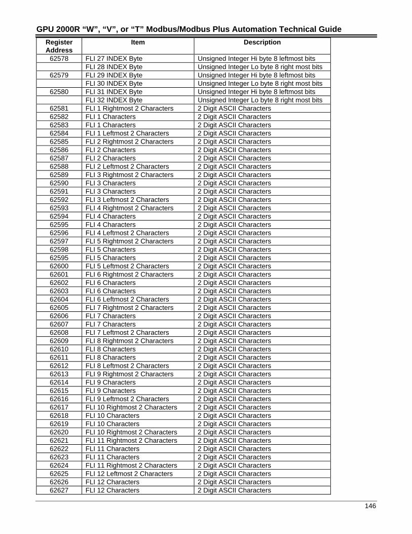
GPU 2000R “W”, “V”, or “T” Modbus/Modbus Plus Automation Technical Guide
146
RegisterAddress
Item Description
62578 FLI 27 INDEX Byte Unsigned Integer Hi byte 8 leftmost bitsFLI 28 INDEX Byte Unsigned Integer Lo byte 8 right most bits
62579 FLI 29 INDEX Byte Unsigned Integer Hi byte 8 leftmost bitsFLI 30 INDEX Byte Unsigned Integer Lo byte 8 right most bits
62580 FLI 31 INDEX Byte Unsigned Integer Hi byte 8 leftmost bitsFLI 32 INDEX Byte Unsigned Integer Lo byte 8 right most bits
62581 FLI 1 Rightmost 2 Characters 2 Digit ASCII Characters62582 FLI 1 Characters 2 Digit ASCII Characters62583 FLI 1 Characters 2 Digit ASCII Characters62584 FLI 1 Leftmost 2 Characters 2 Digit ASCII Characters62585 FLI 2 Rightmost 2 Characters 2 Digit ASCII Characters62586 FLI 2 Characters 2 Digit ASCII Characters62587 FLI 2 Characters 2 Digit ASCII Characters62588 FLI 2 Leftmost 2 Characters 2 Digit ASCII Characters62589 FLI 3 Rightmost 2 Characters 2 Digit ASCII Characters62590 FLI 3 Characters 2 Digit ASCII Characters62591 FLI 3 Characters 2 Digit ASCII Characters62592 FLI 3 Leftmost 2 Characters 2 Digit ASCII Characters62593 FLI 4 Rightmost 2 Characters 2 Digit ASCII Characters62594 FLI 4 Characters 2 Digit ASCII Characters62595 FLI 4 Characters 2 Digit ASCII Characters62596 FLI 4 Leftmost 2 Characters 2 Digit ASCII Characters62597 FLI 5 Rightmost 2 Characters 2 Digit ASCII Characters62598 FLI 5 Characters 2 Digit ASCII Characters62595 FLI 5 Characters 2 Digit ASCII Characters62600 FLI 5 Leftmost 2 Characters 2 Digit ASCII Characters62601 FLI 6 Rightmost 2 Characters 2 Digit ASCII Characters62602 FLI 6 Characters 2 Digit ASCII Characters62603 FLI 6 Characters 2 Digit ASCII Characters62604 FLI 6 Leftmost 2 Characters 2 Digit ASCII Characters62605 FLI 7 Rightmost 2 Characters 2 Digit ASCII Characters62606 FLI 7 Characters 2 Digit ASCII Characters62607 FLI 7 Characters 2 Digit ASCII Characters62608 FLI 7 Leftmost 2 Characters 2 Digit ASCII Characters62609 FLI 8 Rightmost 2 Characters 2 Digit ASCII Characters62610 FLI 8 Characters 2 Digit ASCII Characters62611 FLI 8 Characters 2 Digit ASCII Characters62612 FLI 8 Leftmost 2 Characters 2 Digit ASCII Characters62613 FLI 9 Rightmost 2 Characters 2 Digit ASCII Characters62614 FLI 9 Characters 2 Digit ASCII Characters62615 FLI 9 Characters 2 Digit ASCII Characters62616 FLI 9 Leftmost 2 Characters 2 Digit ASCII Characters62617 FLI 10 Rightmost 2 Characters 2 Digit ASCII Characters62618 FLI 10 Characters 2 Digit ASCII Characters62619 FLI 10 Characters 2 Digit ASCII Characters62620 FLI 10 Rightmost 2 Characters 2 Digit ASCII Characters62621 FLI 11 Rightmost 2 Characters 2 Digit ASCII Characters62622 FLI 11 Characters 2 Digit ASCII Characters62623 FLI 11 Characters 2 Digit ASCII Characters62624 FLI 11 Rightmost 2 Characters 2 Digit ASCII Characters62625 FLI 12 Leftmost 2 Characters 2 Digit ASCII Characters62626 FLI 12 Characters 2 Digit ASCII Characters62627 FLI 12 Characters 2 Digit ASCII Characters
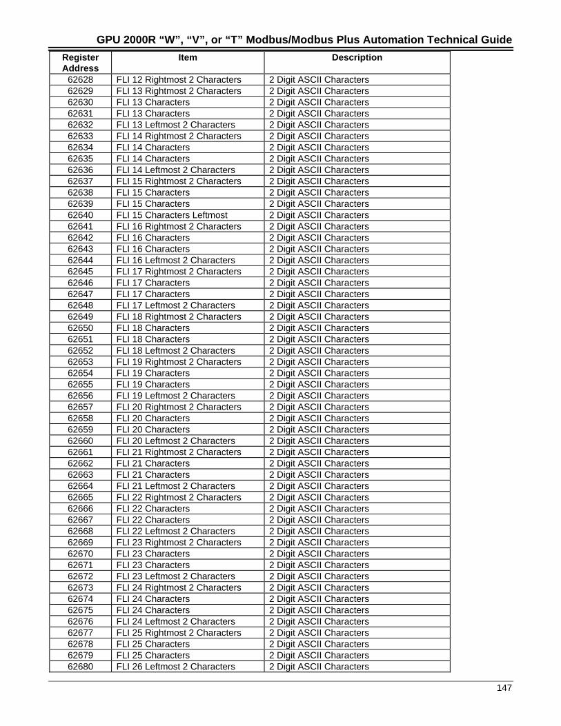
GPU 2000R “W”, “V”, or “T” Modbus/Modbus Plus Automation Technical Guide
147
RegisterAddress
Item Description
62628 FLI 12 Rightmost 2 Characters 2 Digit ASCII Characters62629 FLI 13 Rightmost 2 Characters 2 Digit ASCII Characters62630 FLI 13 Characters 2 Digit ASCII Characters62631 FLI 13 Characters 2 Digit ASCII Characters62632 FLI 13 Leftmost 2 Characters 2 Digit ASCII Characters62633 FLI 14 Rightmost 2 Characters 2 Digit ASCII Characters62634 FLI 14 Characters 2 Digit ASCII Characters62635 FLI 14 Characters 2 Digit ASCII Characters62636 FLI 14 Leftmost 2 Characters 2 Digit ASCII Characters62637 FLI 15 Rightmost 2 Characters 2 Digit ASCII Characters62638 FLI 15 Characters 2 Digit ASCII Characters62639 FLI 15 Characters 2 Digit ASCII Characters62640 FLI 15 Characters Leftmost 2 Digit ASCII Characters62641 FLI 16 Rightmost 2 Characters 2 Digit ASCII Characters62642 FLI 16 Characters 2 Digit ASCII Characters62643 FLI 16 Characters 2 Digit ASCII Characters62644 FLI 16 Leftmost 2 Characters 2 Digit ASCII Characters62645 FLI 17 Rightmost 2 Characters 2 Digit ASCII Characters62646 FLI 17 Characters 2 Digit ASCII Characters62647 FLI 17 Characters 2 Digit ASCII Characters62648 FLI 17 Leftmost 2 Characters 2 Digit ASCII Characters62649 FLI 18 Rightmost 2 Characters 2 Digit ASCII Characters62650 FLI 18 Characters 2 Digit ASCII Characters62651 FLI 18 Characters 2 Digit ASCII Characters62652 FLI 18 Leftmost 2 Characters 2 Digit ASCII Characters62653 FLI 19 Rightmost 2 Characters 2 Digit ASCII Characters62654 FLI 19 Characters 2 Digit ASCII Characters62655 FLI 19 Characters 2 Digit ASCII Characters62656 FLI 19 Leftmost 2 Characters 2 Digit ASCII Characters62657 FLI 20 Rightmost 2 Characters 2 Digit ASCII Characters62658 FLI 20 Characters 2 Digit ASCII Characters62659 FLI 20 Characters 2 Digit ASCII Characters62660 FLI 20 Leftmost 2 Characters 2 Digit ASCII Characters62661 FLI 21 Rightmost 2 Characters 2 Digit ASCII Characters62662 FLI 21 Characters 2 Digit ASCII Characters62663 FLI 21 Characters 2 Digit ASCII Characters62664 FLI 21 Leftmost 2 Characters 2 Digit ASCII Characters62665 FLI 22 Rightmost 2 Characters 2 Digit ASCII Characters62666 FLI 22 Characters 2 Digit ASCII Characters62667 FLI 22 Characters 2 Digit ASCII Characters62668 FLI 22 Leftmost 2 Characters 2 Digit ASCII Characters62669 FLI 23 Rightmost 2 Characters 2 Digit ASCII Characters62670 FLI 23 Characters 2 Digit ASCII Characters62671 FLI 23 Characters 2 Digit ASCII Characters62672 FLI 23 Leftmost 2 Characters 2 Digit ASCII Characters62673 FLI 24 Rightmost 2 Characters 2 Digit ASCII Characters62674 FLI 24 Characters 2 Digit ASCII Characters62675 FLI 24 Characters 2 Digit ASCII Characters62676 FLI 24 Leftmost 2 Characters 2 Digit ASCII Characters62677 FLI 25 Rightmost 2 Characters 2 Digit ASCII Characters62678 FLI 25 Characters 2 Digit ASCII Characters62679 FLI 25 Characters 2 Digit ASCII Characters62680 FLI 26 Leftmost 2 Characters 2 Digit ASCII Characters
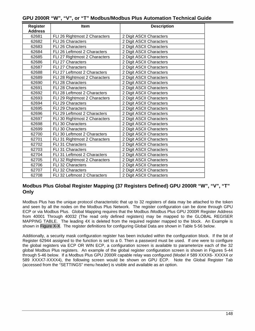
GPU 2000R “W”, “V”, or “T” Modbus/Modbus Plus Automation Technical Guide
148
RegisterAddress
Item Description
62681 FLI 26 Rightmost 2 Characters 2 Digit ASCII Characters62682 FLI 26 Characters 2 Digit ASCII Characters62683 FLI 26 Characters 2 Digit ASCII Characters62684 FLI 26 Leftmost 2 Characters 2 Digit ASCII Characters62685 FLI 27 Rightmost 2 Characters 2 Digit ASCII Characters62686 FLI 27 Characters 2 Digit ASCII Characters62687 FLI 27 Characters 2 Digit ASCII Characters62688 FLI 27 Leftmost 2 Characters 2 Digit ASCII Characters62689 FLI 28 Rightmost 2 Characters 2 Digit ASCII Characters62690 FLI 28 Characters 2 Digit ASCII Characters62691 FLI 28 Characters 2 Digit ASCII Characters62692 FLI 28 Leftmost 2 Characters 2 Digit ASCII Characters62693 FLI 29 Rightmost 2 Characters 2 Digit ASCII Characters62694 FLI 29 Characters 2 Digit ASCII Characters62695 FLI 29 Characters 2 Digit ASCII Characters62696 FLI 29 Leftmost 2 Characters 2 Digit ASCII Characters62697 FLI 30 Rightmost 2 Characters 2 Digit ASCII Characters62698 FLI 30 Characters 2 Digit ASCII Characters62699 FLI 30 Characters 2 Digit ASCII Characters62700 FLI 30 Leftmost 2 Characters 2 Digit ASCII Characters62701 FLI 31 Rightmost 2 Characters 2 Digit ASCII Characters62702 FLI 31 Characters 2 Digit ASCII Characters62703 FLI 31 Characters 2 Digit ASCII Characters62704 FLI 31 Leftmost 2 Characters 2 Digit ASCII Characters62705 FLI 32 Rightmost 2 Characters 2 Digit ASCII Characters62706 FLI 32 Characters 2 Digit ASCII Characters62707 FLI 32 Characters 2 Digit ASCII Characters62708 FLI 32 Leftmost 2 Characters 2 Digit ASCII Characters
Modbus Plus Global Register Mapping (37 Registers Defined) GPU 2000R “W”, “V”, “T”Only
Modbus Plus has the unique protocol characteristic that up to 32 registers of data may be attached to the tokenand seen by all the nodes on the Modbus Plus Network. The register configuration can be done through GPUECP or via Modbus Plus. Global Mapping requires that the Modbus /Modbus Plus GPU 2000R Register Addressfrom 40001 Through 40032 (The read only defined registers) may be mapped to the GLOBAL REGISERMAPPING TABLE. The leading 4X is deleted from the required register mapped to the block. An Example isshown in Figure X-X. The register definitions for configuring Global Data are shown in Table 5-56 below.
Additionally, a security mask configuration register has been included within the configuration block. If the bit ofRegister 62944 assigned to the function is set to a 0. Then a password must be used. If one were to configurethe global registers via ECP OR WIN ECP, a configuration screen is available to parameterize each of the 32global Modbus Plus registers. An example of the global register configuration screen is shown in Figures 5-44through 5-46 below. If a Modbus Plus GPU 2000R capable relay was configured (Model # 589 XXXX6- XXXX4 or589 XXXX7-XXXX4), the following screen would be shown on GPU ECP. Note the Global Register Tab(accessed from the “SETTINGS” menu header) is visible and available as an option.
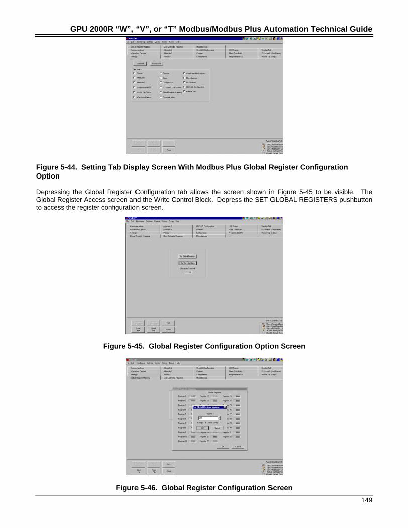
GPU 2000R “W”, “V”, or “T” Modbus/Modbus Plus Automation Technical Guide
149
Figure 5-44. Setting Tab Display Screen With Modbus Plus Global Register ConfigurationOption
Depressing the Global Register Configuration tab allows the screen shown in Figure 5-45 to be visible. TheGlobal Register Access screen and the Write Control Block. Depress the SET GLOBAL REGISTERS pushbuttonto access the register configuration screen.
Figure 5-45. Global Register Configuration Option Screen
Figure 5-46. Global Register Configuration Screen
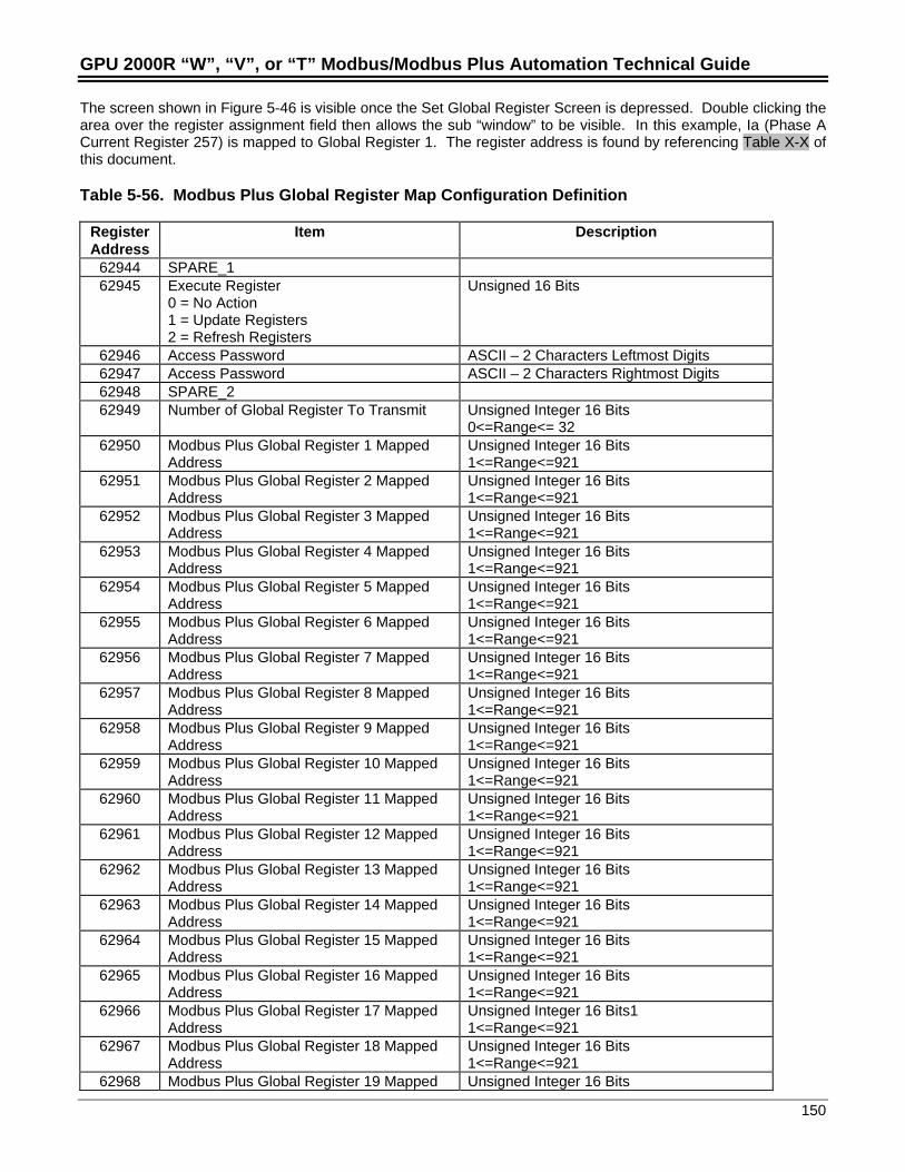
GPU 2000R “W”, “V”, or “T” Modbus/Modbus Plus Automation Technical Guide
150
The screen shown in Figure 5-46 is visible once the Set Global Register Screen is depressed. Double clicking thearea over the register assignment field then allows the sub “window” to be visible. In this example, Ia (Phase ACurrent Register 257) is mapped to Global Register 1. The register address is found by referencing Table X-X ofthis document.
Table 5-56. Modbus Plus Global Register Map Configuration Definition
RegisterAddress
Item Description
62944 SPARE_162945 Execute Register
0 = No Action1 = Update Registers2 = Refresh Registers
Unsigned 16 Bits
62946 Access Password ASCII – 2 Characters Leftmost Digits62947 Access Password ASCII – 2 Characters Rightmost Digits62948 SPARE_262949 Number of Global Register To Transmit Unsigned Integer 16 Bits
0<=Range<= 3262950 Modbus Plus Global Register 1 Mapped
AddressUnsigned Integer 16 Bits1<=Range<=921
62951 Modbus Plus Global Register 2 MappedAddress
Unsigned Integer 16 Bits1<=Range<=921
62952 Modbus Plus Global Register 3 MappedAddress
Unsigned Integer 16 Bits1<=Range<=921
62953 Modbus Plus Global Register 4 MappedAddress
Unsigned Integer 16 Bits1<=Range<=921
62954 Modbus Plus Global Register 5 MappedAddress
Unsigned Integer 16 Bits1<=Range<=921
62955 Modbus Plus Global Register 6 MappedAddress
Unsigned Integer 16 Bits1<=Range<=921
62956 Modbus Plus Global Register 7 MappedAddress
Unsigned Integer 16 Bits1<=Range<=921
62957 Modbus Plus Global Register 8 MappedAddress
Unsigned Integer 16 Bits1<=Range<=921
62958 Modbus Plus Global Register 9 MappedAddress
Unsigned Integer 16 Bits1<=Range<=921
62959 Modbus Plus Global Register 10 MappedAddress
Unsigned Integer 16 Bits1<=Range<=921
62960 Modbus Plus Global Register 11 MappedAddress
Unsigned Integer 16 Bits1<=Range<=921
62961 Modbus Plus Global Register 12 MappedAddress
Unsigned Integer 16 Bits1<=Range<=921
62962 Modbus Plus Global Register 13 MappedAddress
Unsigned Integer 16 Bits1<=Range<=921
62963 Modbus Plus Global Register 14 MappedAddress
Unsigned Integer 16 Bits1<=Range<=921
62964 Modbus Plus Global Register 15 MappedAddress
Unsigned Integer 16 Bits1<=Range<=921
62965 Modbus Plus Global Register 16 MappedAddress
Unsigned Integer 16 Bits1<=Range<=921
62966 Modbus Plus Global Register 17 MappedAddress
Unsigned Integer 16 Bits11<=Range<=921
62967 Modbus Plus Global Register 18 MappedAddress
Unsigned Integer 16 Bits1<=Range<=921
62968 Modbus Plus Global Register 19 Mapped Unsigned Integer 16 Bits
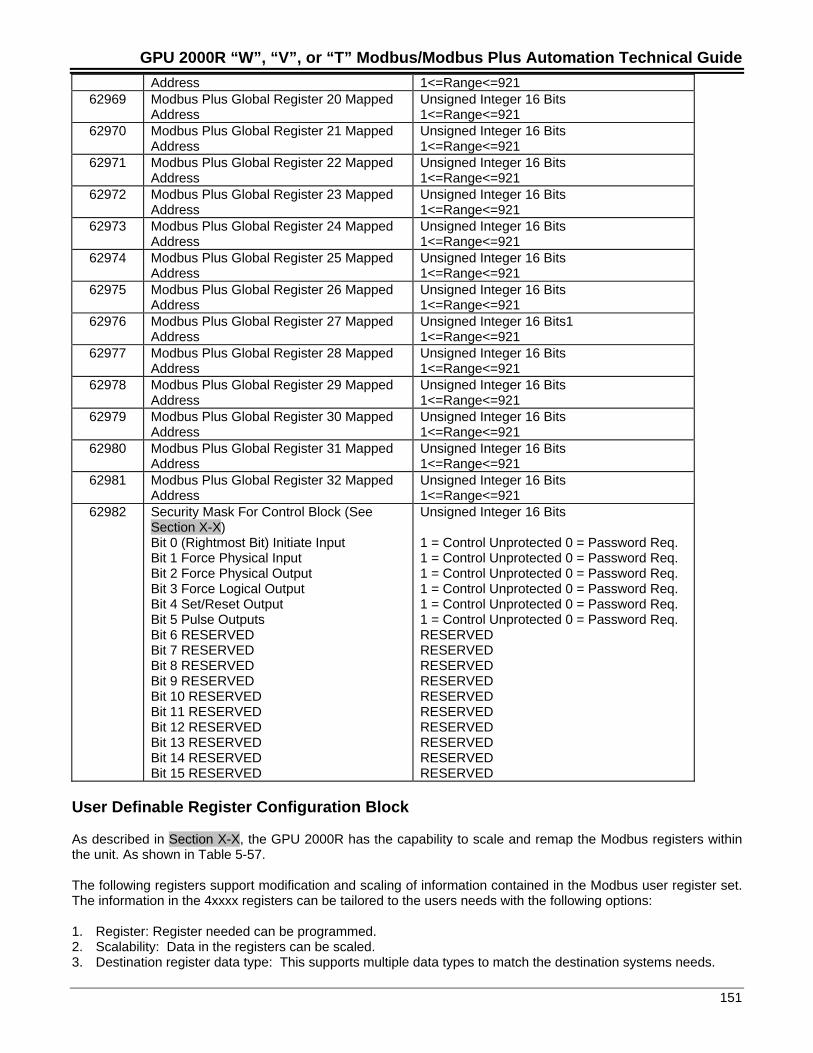
GPU 2000R “W”, “V”, or “T” Modbus/Modbus Plus Automation Technical Guide
151
Address 1<=Range<=92162969 Modbus Plus Global Register 20 Mapped
AddressUnsigned Integer 16 Bits1<=Range<=921
62970 Modbus Plus Global Register 21 MappedAddress
Unsigned Integer 16 Bits1<=Range<=921
62971 Modbus Plus Global Register 22 MappedAddress
Unsigned Integer 16 Bits1<=Range<=921
62972 Modbus Plus Global Register 23 MappedAddress
Unsigned Integer 16 Bits1<=Range<=921
62973 Modbus Plus Global Register 24 MappedAddress
Unsigned Integer 16 Bits1<=Range<=921
62974 Modbus Plus Global Register 25 MappedAddress
Unsigned Integer 16 Bits1<=Range<=921
62975 Modbus Plus Global Register 26 MappedAddress
Unsigned Integer 16 Bits1<=Range<=921
62976 Modbus Plus Global Register 27 MappedAddress
Unsigned Integer 16 Bits11<=Range<=921
62977 Modbus Plus Global Register 28 MappedAddress
Unsigned Integer 16 Bits1<=Range<=921
62978 Modbus Plus Global Register 29 MappedAddress
Unsigned Integer 16 Bits1<=Range<=921
62979 Modbus Plus Global Register 30 MappedAddress
Unsigned Integer 16 Bits1<=Range<=921
62980 Modbus Plus Global Register 31 MappedAddress
Unsigned Integer 16 Bits1<=Range<=921
62981 Modbus Plus Global Register 32 MappedAddress
Unsigned Integer 16 Bits1<=Range<=921
62982 Security Mask For Control Block (SeeSection X-X)Bit 0 (Rightmost Bit) Initiate InputBit 1 Force Physical InputBit 2 Force Physical OutputBit 3 Force Logical OutputBit 4 Set/Reset OutputBit 5 Pulse OutputsBit 6 RESERVEDBit 7 RESERVEDBit 8 RESERVEDBit 9 RESERVEDBit 10 RESERVEDBit 11 RESERVEDBit 12 RESERVEDBit 13 RESERVEDBit 14 RESERVEDBit 15 RESERVED
Unsigned Integer 16 Bits
1 = Control Unprotected 0 = Password Req.1 = Control Unprotected 0 = Password Req.1 = Control Unprotected 0 = Password Req.1 = Control Unprotected 0 = Password Req.1 = Control Unprotected 0 = Password Req.1 = Control Unprotected 0 = Password Req.RESERVEDRESERVEDRESERVEDRESERVEDRESERVEDRESERVEDRESERVEDRESERVEDRESERVEDRESERVED
User Definable Register Configuration Block
As described in Section X-X, the GPU 2000R has the capability to scale and remap the Modbus registers withinthe unit. As shown in Table 5-57.
The following registers support modification and scaling of information contained in the Modbus user register set.The information in the 4xxxx registers can be tailored to the users needs with the following options:
1. Register: Register needed can be programmed.2. Scalability: Data in the registers can be scaled.3. Destination register data type: This supports multiple data types to match the destination systems needs.
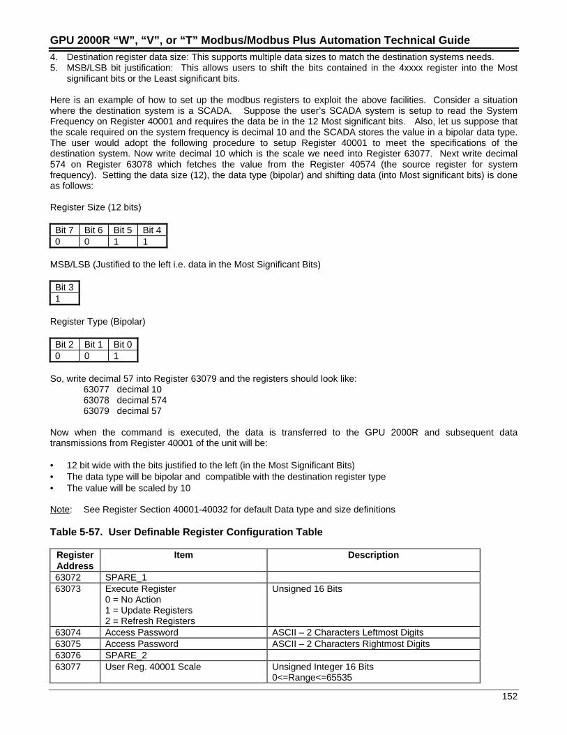
GPU 2000R “W”, “V”, or “T” Modbus/Modbus Plus Automation Technical Guide
152
4. Destination register data size: This supports multiple data sizes to match the destination systems needs.5. MSB/LSB bit justification: This allows users to shift the bits contained in the 4xxxx register into the Most
significant bits or the Least significant bits.
Here is an example of how to set up the modbus registers to exploit the above facilities. Consider a situationwhere the destination system is a SCADA. Suppose the user’s SCADA system is setup to read the SystemFrequency on Register 40001 and requires the data be in the 12 Most significant bits. Also, let us suppose thatthe scale required on the system frequency is decimal 10 and the SCADA stores the value in a bipolar data type.The user would adopt the following procedure to setup Register 40001 to meet the specifications of thedestination system. Now write decimal 10 which is the scale we need into Register 63077. Next write decimal574 on Register 63078 which fetches the value from the Register 40574 (the source register for systemfrequency). Setting the data size (12), the data type (bipolar) and shifting data (into Most significant bits) is doneas follows:
Register Size (12 bits)
Bit 7 Bit 6 Bit 5 Bit 40 0 1 1
MSB/LSB (Justified to the left i.e. data in the Most Significant Bits)
Bit 31
Register Type (Bipolar)
Bit 2 Bit 1 Bit 00 0 1
So, write decimal 57 into Register 63079 and the registers should look like:63077 decimal 1063078 decimal 57463079 decimal 57
Now when the command is executed, the data is transferred to the GPU 2000R and subsequent datatransmissions from Register 40001 of the unit will be:
• 12 bit wide with the bits justified to the left (in the Most Significant Bits)• The data type will be bipolar and compatible with the destination register type• The value will be scaled by 10
Note: See Register Section 40001-40032 for default Data type and size definitions
Table 5-57. User Definable Register Configuration Table
RegisterAddress
Item Description
63072 SPARE_163073 Execute Register
0 = No Action1 = Update Registers2 = Refresh Registers
Unsigned 16 Bits
63074 Access Password ASCII – 2 Characters Leftmost Digits63075 Access Password ASCII – 2 Characters Rightmost Digits63076 SPARE_263077 User Reg. 40001 Scale Unsigned Integer 16 Bits
0<=Range<=65535
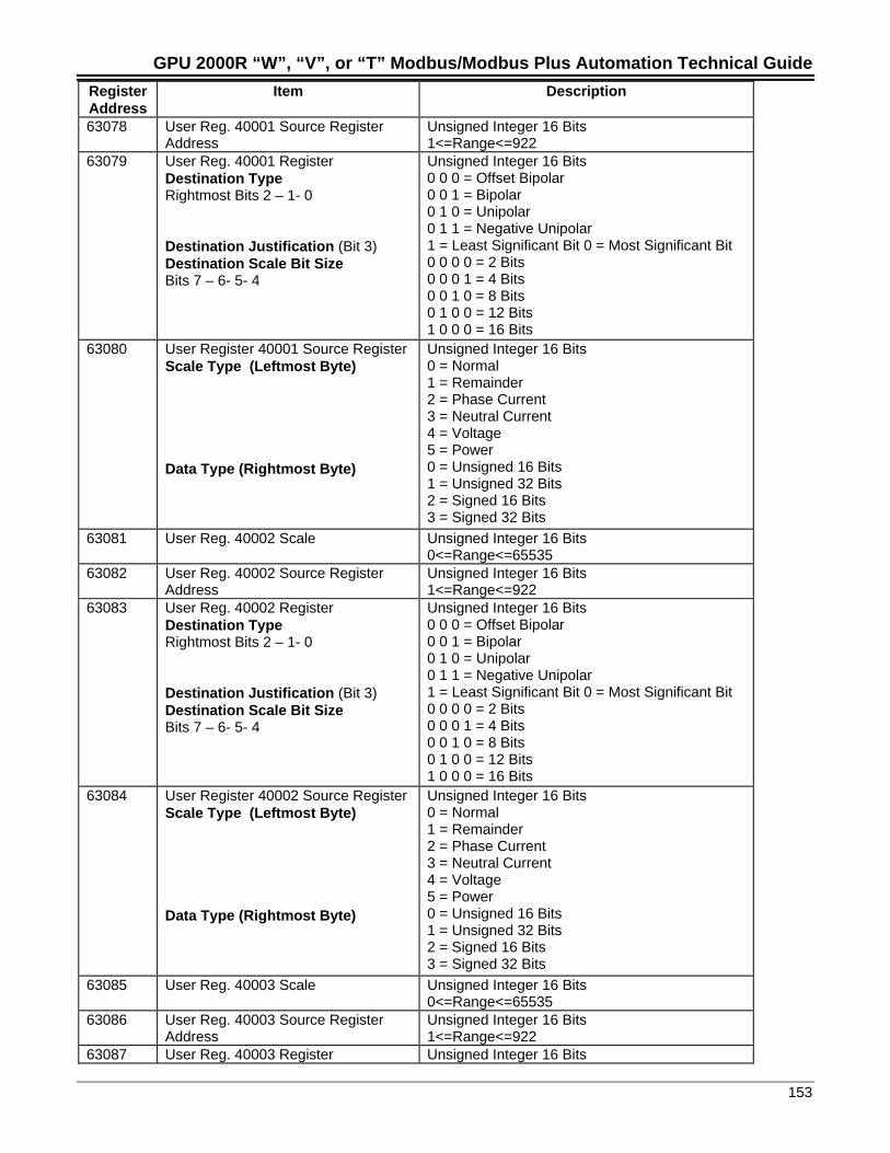
GPU 2000R “W”, “V”, or “T” Modbus/Modbus Plus Automation Technical Guide
153
RegisterAddress
Item Description
63078 User Reg. 40001 Source RegisterAddress
Unsigned Integer 16 Bits1<=Range<=922
63079 User Reg. 40001 RegisterDestination TypeRightmost Bits 2 – 1- 0
Destination Justification (Bit 3)Destination Scale Bit SizeBits 7 – 6- 5- 4
Unsigned Integer 16 Bits0 0 0 = Offset Bipolar0 0 1 = Bipolar0 1 0 = Unipolar0 1 1 = Negative Unipolar1 = Least Significant Bit 0 = Most Significant Bit0 0 0 0 = 2 Bits0 0 0 1 = 4 Bits0 0 1 0 = 8 Bits0 1 0 0 = 12 Bits1 0 0 0 = 16 Bits
63080 User Register 40001 Source RegisterScale Type (Leftmost Byte)
Data Type (Rightmost Byte)
Unsigned Integer 16 Bits0 = Normal1 = Remainder2 = Phase Current3 = Neutral Current4 = Voltage5 = Power0 = Unsigned 16 Bits1 = Unsigned 32 Bits2 = Signed 16 Bits3 = Signed 32 Bits
63081 User Reg. 40002 Scale Unsigned Integer 16 Bits0<=Range<=65535
63082 User Reg. 40002 Source RegisterAddress
Unsigned Integer 16 Bits1<=Range<=922
63083 User Reg. 40002 RegisterDestination TypeRightmost Bits 2 – 1- 0
Destination Justification (Bit 3)Destination Scale Bit SizeBits 7 – 6- 5- 4
Unsigned Integer 16 Bits0 0 0 = Offset Bipolar0 0 1 = Bipolar0 1 0 = Unipolar0 1 1 = Negative Unipolar1 = Least Significant Bit 0 = Most Significant Bit0 0 0 0 = 2 Bits0 0 0 1 = 4 Bits0 0 1 0 = 8 Bits0 1 0 0 = 12 Bits1 0 0 0 = 16 Bits
63084 User Register 40002 Source RegisterScale Type (Leftmost Byte)
Data Type (Rightmost Byte)
Unsigned Integer 16 Bits0 = Normal1 = Remainder2 = Phase Current3 = Neutral Current4 = Voltage5 = Power0 = Unsigned 16 Bits1 = Unsigned 32 Bits2 = Signed 16 Bits3 = Signed 32 Bits
63085 User Reg. 40003 Scale Unsigned Integer 16 Bits0<=Range<=65535
63086 User Reg. 40003 Source RegisterAddress
Unsigned Integer 16 Bits1<=Range<=922
63087 User Reg. 40003 Register Unsigned Integer 16 Bits
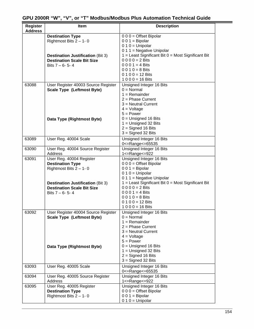
GPU 2000R “W”, “V”, or “T” Modbus/Modbus Plus Automation Technical Guide
154
RegisterAddress
Item Description
Destination TypeRightmost Bits 2 – 1- 0
Destination Justification (Bit 3)Destination Scale Bit SizeBits 7 – 6- 5- 4
0 0 0 = Offset Bipolar0 0 1 = Bipolar0 1 0 = Unipolar0 1 1 = Negative Unipolar1 = Least Significant Bit 0 = Most Significant Bit0 0 0 0 = 2 Bits0 0 0 1 = 4 Bits0 0 1 0 = 8 Bits0 1 0 0 = 12 Bits1 0 0 0 = 16 Bits
63088 User Register 40003 Source RegisterScale Type (Leftmost Byte)
Data Type (Rightmost Byte)
Unsigned Integer 16 Bits0 = Normal1 = Remainder2 = Phase Current3 = Neutral Current4 = Voltage5 = Power0 = Unsigned 16 Bits1 = Unsigned 32 Bits2 = Signed 16 Bits3 = Signed 32 Bits
63089 User Reg. 40004 Scale Unsigned Integer 16 Bits0<=Range<=65535
63090 User Reg. 40004 Source RegisterAddress
Unsigned Integer 16 Bits1<=Range<=922
63091 User Reg. 40004 RegisterDestination TypeRightmost Bits 2 – 1- 0
Destination Justification (Bit 3)Destination Scale Bit SizeBits 7 – 6- 5- 4
Unsigned Integer 16 Bits0 0 0 = Offset Bipolar0 0 1 = Bipolar0 1 0 = Unipolar0 1 1 = Negative Unipolar1 = Least Significant Bit 0 = Most Significant Bit0 0 0 0 = 2 Bits0 0 0 1 = 4 Bits0 0 1 0 = 8 Bits0 1 0 0 = 12 Bits1 0 0 0 = 16 Bits
63092 User Register 40004 Source RegisterScale Type (Leftmost Byte)
Data Type (Rightmost Byte)
Unsigned Integer 16 Bits0 = Normal1 = Remainder2 = Phase Current3 = Neutral Current4 = Voltage5 = Power0 = Unsigned 16 Bits1 = Unsigned 32 Bits2 = Signed 16 Bits3 = Signed 32 Bits
63093 User Reg. 40005 Scale Unsigned Integer 16 Bits0<=Range<=65535
63094 User Reg. 40005 Source RegisterAddress
Unsigned Integer 16 Bits1<=Range<=922
63095 User Reg. 40005 RegisterDestination TypeRightmost Bits 2 – 1- 0
Unsigned Integer 16 Bits0 0 0 = Offset Bipolar0 0 1 = Bipolar0 1 0 = Unipolar
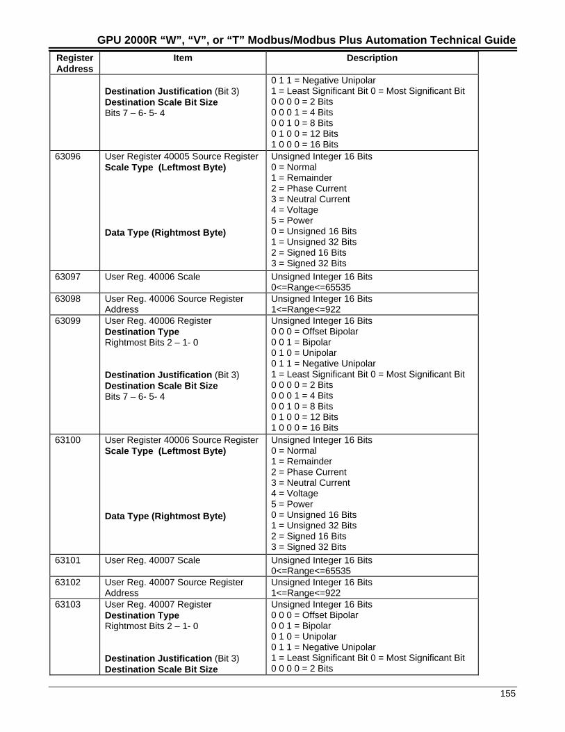
GPU 2000R “W”, “V”, or “T” Modbus/Modbus Plus Automation Technical Guide
155
RegisterAddress
Item Description
Destination Justification (Bit 3)Destination Scale Bit SizeBits 7 – 6- 5- 4
0 1 1 = Negative Unipolar1 = Least Significant Bit 0 = Most Significant Bit0 0 0 0 = 2 Bits0 0 0 1 = 4 Bits0 0 1 0 = 8 Bits0 1 0 0 = 12 Bits1 0 0 0 = 16 Bits
63096 User Register 40005 Source RegisterScale Type (Leftmost Byte)
Data Type (Rightmost Byte)
Unsigned Integer 16 Bits0 = Normal1 = Remainder2 = Phase Current3 = Neutral Current4 = Voltage5 = Power0 = Unsigned 16 Bits1 = Unsigned 32 Bits2 = Signed 16 Bits3 = Signed 32 Bits
63097 User Reg. 40006 Scale Unsigned Integer 16 Bits0<=Range<=65535
63098 User Reg. 40006 Source RegisterAddress
Unsigned Integer 16 Bits1<=Range<=922
63099 User Reg. 40006 RegisterDestination TypeRightmost Bits 2 – 1- 0
Destination Justification (Bit 3)Destination Scale Bit SizeBits 7 – 6- 5- 4
Unsigned Integer 16 Bits0 0 0 = Offset Bipolar0 0 1 = Bipolar0 1 0 = Unipolar0 1 1 = Negative Unipolar1 = Least Significant Bit 0 = Most Significant Bit0 0 0 0 = 2 Bits0 0 0 1 = 4 Bits0 0 1 0 = 8 Bits0 1 0 0 = 12 Bits1 0 0 0 = 16 Bits
63100 User Register 40006 Source RegisterScale Type (Leftmost Byte)
Data Type (Rightmost Byte)
Unsigned Integer 16 Bits0 = Normal1 = Remainder2 = Phase Current3 = Neutral Current4 = Voltage5 = Power0 = Unsigned 16 Bits1 = Unsigned 32 Bits2 = Signed 16 Bits3 = Signed 32 Bits
63101 User Reg. 40007 Scale Unsigned Integer 16 Bits0<=Range<=65535
63102 User Reg. 40007 Source RegisterAddress
Unsigned Integer 16 Bits1<=Range<=922
63103 User Reg. 40007 RegisterDestination TypeRightmost Bits 2 – 1- 0
Destination Justification (Bit 3)Destination Scale Bit Size
Unsigned Integer 16 Bits0 0 0 = Offset Bipolar0 0 1 = Bipolar0 1 0 = Unipolar0 1 1 = Negative Unipolar1 = Least Significant Bit 0 = Most Significant Bit0 0 0 0 = 2 Bits
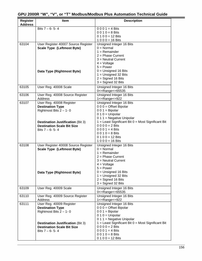
GPU 2000R “W”, “V”, or “T” Modbus/Modbus Plus Automation Technical Guide
156
RegisterAddress
Item Description
Bits 7 – 6- 5- 4 0 0 0 1 = 4 Bits0 0 1 0 = 8 Bits0 1 0 0 = 12 Bits1 0 0 0 = 16 Bits
63104 User Register 40007 Source RegisterScale Type (Leftmost Byte)
Data Type (Rightmost Byte)
Unsigned Integer 16 Bits0 = Normal1 = Remainder2 = Phase Current3 = Neutral Current4 = Voltage5 = Power0 = Unsigned 16 Bits1 = Unsigned 32 Bits2 = Signed 16 Bits3 = Signed 32 Bits
63105 User Reg. 40008 Scale Unsigned Integer 16 Bits0<=Range<=65535
63106 User Reg. 40008 Source RegisterAddress
Unsigned Integer 16 Bits1<=Range<=922
63107 User Reg. 40008 RegisterDestination TypeRightmost Bits 2 – 1- 0
Destination Justification (Bit 3)Destination Scale Bit SizeBits 7 – 6- 5- 4
Unsigned Integer 16 Bits0 0 0 = Offset Bipolar0 0 1 = Bipolar0 1 0 = Unipolar0 1 1 = Negative Unipolar1 = Least Significant Bit 0 = Most Significant Bit0 0 0 0 = 2 Bits0 0 0 1 = 4 Bits0 0 1 0 = 8 Bits0 1 0 0 = 12 Bits1 0 0 0 = 16 Bits
63108 User Register 40008 Source RegisterScale Type (Leftmost Byte)
Data Type (Rightmost Byte)
Unsigned Integer 16 Bits0 = Normal1 = Remainder2 = Phase Current3 = Neutral Current4 = Voltage5 = Power0 = Unsigned 16 Bits1 = Unsigned 32 Bits2 = Signed 16 Bits3 = Signed 32 Bits
63109 User Reg. 40009 Scale Unsigned Integer 16 Bits0<=Range<=65535
63110 User Reg. 40009 Source RegisterAddress
Unsigned Integer 16 Bits1<=Range<=922
63111 User Reg. 40009 RegisterDestination TypeRightmost Bits 2 – 1- 0
Destination Justification (Bit 3)Destination Scale Bit SizeBits 7 – 6- 5- 4
Unsigned Integer 16 Bits0 0 0 = Offset Bipolar0 0 1 = Bipolar0 1 0 = Unipolar0 1 1 = Negative Unipolar1 = Least Significant Bit 0 = Most Significant Bit0 0 0 0 = 2 Bits0 0 0 1 = 4 Bits0 0 1 0 = 8 Bits0 1 0 0 = 12 Bits
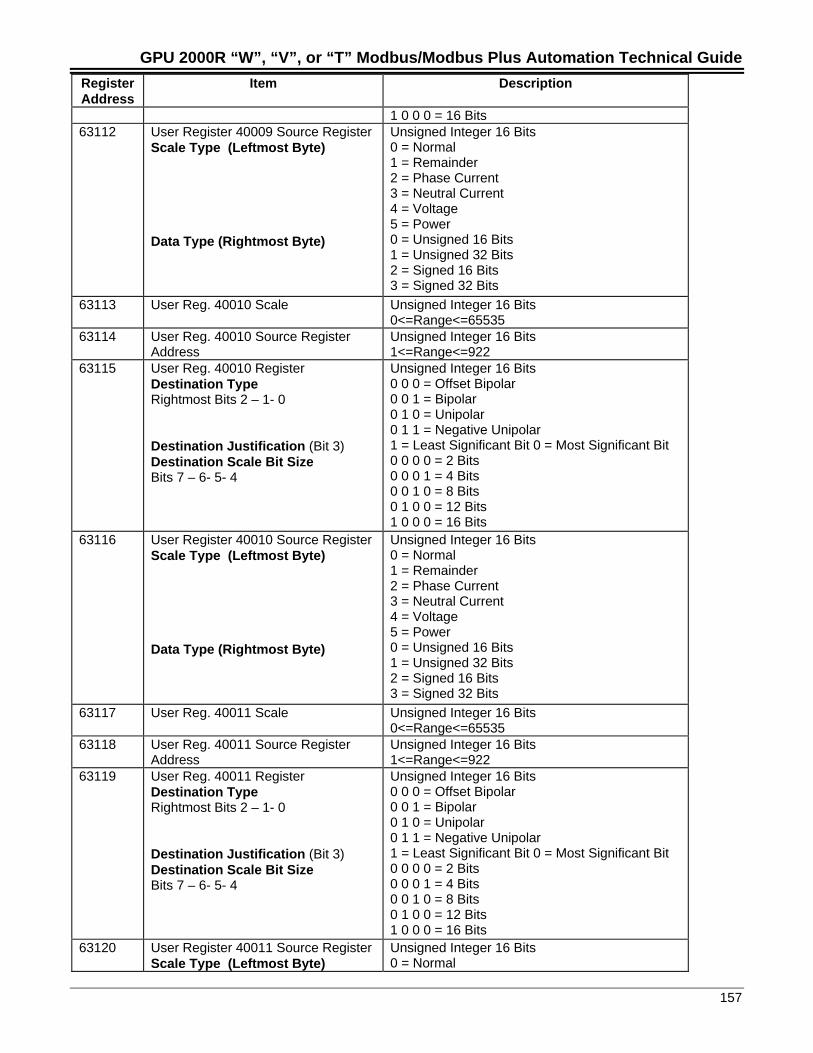
GPU 2000R “W”, “V”, or “T” Modbus/Modbus Plus Automation Technical Guide
157
RegisterAddress
Item Description
1 0 0 0 = 16 Bits63112 User Register 40009 Source Register
Scale Type (Leftmost Byte)
Data Type (Rightmost Byte)
Unsigned Integer 16 Bits0 = Normal1 = Remainder2 = Phase Current3 = Neutral Current4 = Voltage5 = Power0 = Unsigned 16 Bits1 = Unsigned 32 Bits2 = Signed 16 Bits3 = Signed 32 Bits
63113 User Reg. 40010 Scale Unsigned Integer 16 Bits0<=Range<=65535
63114 User Reg. 40010 Source RegisterAddress
Unsigned Integer 16 Bits1<=Range<=922
63115 User Reg. 40010 RegisterDestination TypeRightmost Bits 2 – 1- 0
Destination Justification (Bit 3)Destination Scale Bit SizeBits 7 – 6- 5- 4
Unsigned Integer 16 Bits0 0 0 = Offset Bipolar0 0 1 = Bipolar0 1 0 = Unipolar0 1 1 = Negative Unipolar1 = Least Significant Bit 0 = Most Significant Bit0 0 0 0 = 2 Bits0 0 0 1 = 4 Bits0 0 1 0 = 8 Bits0 1 0 0 = 12 Bits1 0 0 0 = 16 Bits
63116 User Register 40010 Source RegisterScale Type (Leftmost Byte)
Data Type (Rightmost Byte)
Unsigned Integer 16 Bits0 = Normal1 = Remainder2 = Phase Current3 = Neutral Current4 = Voltage5 = Power0 = Unsigned 16 Bits1 = Unsigned 32 Bits2 = Signed 16 Bits3 = Signed 32 Bits
63117 User Reg. 40011 Scale Unsigned Integer 16 Bits0<=Range<=65535
63118 User Reg. 40011 Source RegisterAddress
Unsigned Integer 16 Bits1<=Range<=922
63119 User Reg. 40011 RegisterDestination TypeRightmost Bits 2 – 1- 0
Destination Justification (Bit 3)Destination Scale Bit SizeBits 7 – 6- 5- 4
Unsigned Integer 16 Bits0 0 0 = Offset Bipolar0 0 1 = Bipolar0 1 0 = Unipolar0 1 1 = Negative Unipolar1 = Least Significant Bit 0 = Most Significant Bit0 0 0 0 = 2 Bits0 0 0 1 = 4 Bits0 0 1 0 = 8 Bits0 1 0 0 = 12 Bits1 0 0 0 = 16 Bits
63120 User Register 40011 Source RegisterScale Type (Leftmost Byte)
Unsigned Integer 16 Bits0 = Normal
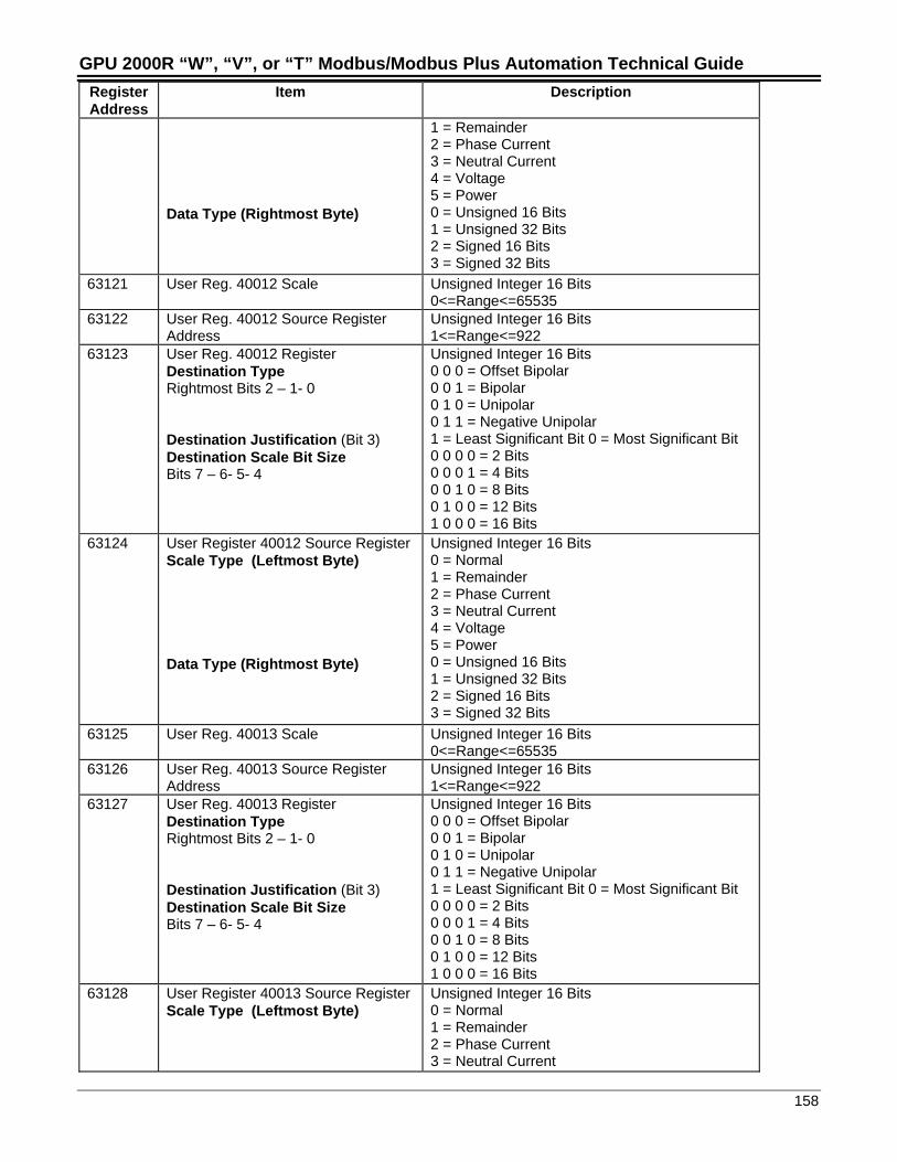
GPU 2000R “W”, “V”, or “T” Modbus/Modbus Plus Automation Technical Guide
158
RegisterAddress
Item Description
Data Type (Rightmost Byte)
1 = Remainder2 = Phase Current3 = Neutral Current4 = Voltage5 = Power0 = Unsigned 16 Bits1 = Unsigned 32 Bits2 = Signed 16 Bits3 = Signed 32 Bits
63121 User Reg. 40012 Scale Unsigned Integer 16 Bits0<=Range<=65535
63122 User Reg. 40012 Source RegisterAddress
Unsigned Integer 16 Bits1<=Range<=922
63123 User Reg. 40012 RegisterDestination TypeRightmost Bits 2 – 1- 0
Destination Justification (Bit 3)Destination Scale Bit SizeBits 7 – 6- 5- 4
Unsigned Integer 16 Bits0 0 0 = Offset Bipolar0 0 1 = Bipolar0 1 0 = Unipolar0 1 1 = Negative Unipolar1 = Least Significant Bit 0 = Most Significant Bit0 0 0 0 = 2 Bits0 0 0 1 = 4 Bits0 0 1 0 = 8 Bits0 1 0 0 = 12 Bits1 0 0 0 = 16 Bits
63124 User Register 40012 Source RegisterScale Type (Leftmost Byte)
Data Type (Rightmost Byte)
Unsigned Integer 16 Bits0 = Normal1 = Remainder2 = Phase Current3 = Neutral Current4 = Voltage5 = Power0 = Unsigned 16 Bits1 = Unsigned 32 Bits2 = Signed 16 Bits3 = Signed 32 Bits
63125 User Reg. 40013 Scale Unsigned Integer 16 Bits0<=Range<=65535
63126 User Reg. 40013 Source RegisterAddress
Unsigned Integer 16 Bits1<=Range<=922
63127 User Reg. 40013 RegisterDestination TypeRightmost Bits 2 – 1- 0
Destination Justification (Bit 3)Destination Scale Bit SizeBits 7 – 6- 5- 4
Unsigned Integer 16 Bits0 0 0 = Offset Bipolar0 0 1 = Bipolar0 1 0 = Unipolar0 1 1 = Negative Unipolar1 = Least Significant Bit 0 = Most Significant Bit0 0 0 0 = 2 Bits0 0 0 1 = 4 Bits0 0 1 0 = 8 Bits0 1 0 0 = 12 Bits1 0 0 0 = 16 Bits
63128 User Register 40013 Source RegisterScale Type (Leftmost Byte)
Unsigned Integer 16 Bits0 = Normal1 = Remainder2 = Phase Current3 = Neutral Current
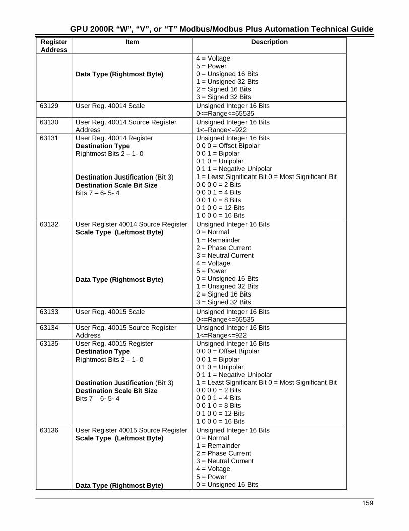
GPU 2000R “W”, “V”, or “T” Modbus/Modbus Plus Automation Technical Guide
159
RegisterAddress
Item Description
Data Type (Rightmost Byte)
4 = Voltage5 = Power0 = Unsigned 16 Bits1 = Unsigned 32 Bits2 = Signed 16 Bits3 = Signed 32 Bits
63129 User Reg. 40014 Scale Unsigned Integer 16 Bits0<=Range<=65535
63130 User Reg. 40014 Source RegisterAddress
Unsigned Integer 16 Bits1<=Range<=922
63131 User Reg. 40014 RegisterDestination TypeRightmost Bits 2 – 1- 0
Destination Justification (Bit 3)Destination Scale Bit SizeBits 7 – 6- 5- 4
Unsigned Integer 16 Bits0 0 0 = Offset Bipolar0 0 1 = Bipolar0 1 0 = Unipolar0 1 1 = Negative Unipolar1 = Least Significant Bit 0 = Most Significant Bit0 0 0 0 = 2 Bits0 0 0 1 = 4 Bits0 0 1 0 = 8 Bits0 1 0 0 = 12 Bits1 0 0 0 = 16 Bits
63132 User Register 40014 Source RegisterScale Type (Leftmost Byte)
Data Type (Rightmost Byte)
Unsigned Integer 16 Bits0 = Normal1 = Remainder2 = Phase Current3 = Neutral Current4 = Voltage5 = Power0 = Unsigned 16 Bits1 = Unsigned 32 Bits2 = Signed 16 Bits3 = Signed 32 Bits
63133 User Reg. 40015 Scale Unsigned Integer 16 Bits0<=Range<=65535
63134 User Reg. 40015 Source RegisterAddress
Unsigned Integer 16 Bits1<=Range<=922
63135 User Reg. 40015 RegisterDestination TypeRightmost Bits 2 – 1- 0
Destination Justification (Bit 3)Destination Scale Bit SizeBits 7 – 6- 5- 4
Unsigned Integer 16 Bits0 0 0 = Offset Bipolar0 0 1 = Bipolar0 1 0 = Unipolar0 1 1 = Negative Unipolar1 = Least Significant Bit 0 = Most Significant Bit0 0 0 0 = 2 Bits0 0 0 1 = 4 Bits0 0 1 0 = 8 Bits0 1 0 0 = 12 Bits1 0 0 0 = 16 Bits
63136 User Register 40015 Source RegisterScale Type (Leftmost Byte)
Data Type (Rightmost Byte)
Unsigned Integer 16 Bits0 = Normal1 = Remainder2 = Phase Current3 = Neutral Current4 = Voltage5 = Power0 = Unsigned 16 Bits
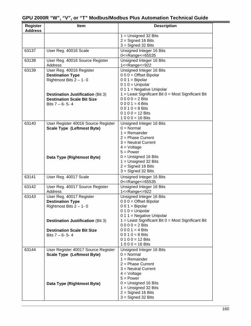
GPU 2000R “W”, “V”, or “T” Modbus/Modbus Plus Automation Technical Guide
160
RegisterAddress
Item Description
1 = Unsigned 32 Bits2 = Signed 16 Bits3 = Signed 32 Bits
63137 User Reg. 40016 Scale Unsigned Integer 16 Bits0<=Range<=65535
63138 User Reg. 40016 Source RegisterAddress
Unsigned Integer 16 Bits1<=Range<=922
63139 User Reg. 40016 RegisterDestination TypeRightmost Bits 2 – 1- 0
Destination Justification (Bit 3)Destination Scale Bit SizeBits 7 – 6- 5- 4
Unsigned Integer 16 Bits0 0 0 = Offset Bipolar0 0 1 = Bipolar0 1 0 = Unipolar0 1 1 = Negative Unipolar1 = Least Significant Bit 0 = Most Significant Bit0 0 0 0 = 2 Bits0 0 0 1 = 4 Bits0 0 1 0 = 8 Bits0 1 0 0 = 12 Bits1 0 0 0 = 16 Bits
63140 User Register 40016 Source RegisterScale Type (Leftmost Byte)
Data Type (Rightmost Byte)
Unsigned Integer 16 Bits0 = Normal1 = Remainder2 = Phase Current3 = Neutral Current4 = Voltage5 = Power0 = Unsigned 16 Bits1 = Unsigned 32 Bits2 = Signed 16 Bits3 = Signed 32 Bits
63141 User Reg. 40017 Scale Unsigned Integer 16 Bits0<=Range<=65535
63142 User Reg. 40017 Source RegisterAddress
Unsigned Integer 16 Bits1<=Range<=922
63143 User Reg. 40017 RegisterDestination TypeRightmost Bits 2 – 1- 0
Destination Justification (Bit 3)
Destination Scale Bit SizeBits 7 – 6- 5- 4
Unsigned Integer 16 Bits0 0 0 = Offset Bipolar0 0 1 = Bipolar0 1 0 = Unipolar0 1 1 = Negative Unipolar1 = Least Significant Bit 0 = Most Significant Bit0 0 0 0 = 2 Bits0 0 0 1 = 4 Bits0 0 1 0 = 8 Bits0 1 0 0 = 12 Bits1 0 0 0 = 16 Bits
63144 User Register 40017 Source RegisterScale Type (Leftmost Byte)
Data Type (Rightmost Byte)
Unsigned Integer 16 Bits0 = Normal1 = Remainder2 = Phase Current3 = Neutral Current4 = Voltage5 = Power0 = Unsigned 16 Bits1 = Unsigned 32 Bits2 = Signed 16 Bits3 = Signed 32 Bits
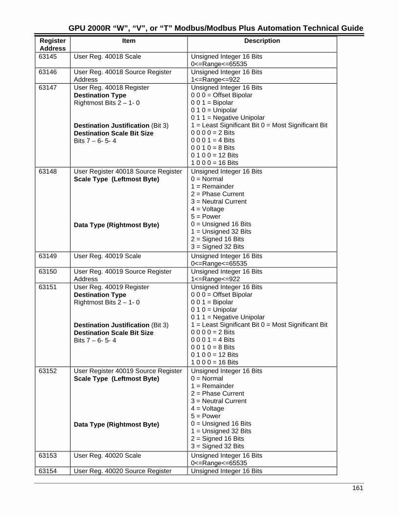
GPU 2000R “W”, “V”, or “T” Modbus/Modbus Plus Automation Technical Guide
161
RegisterAddress
Item Description
63145 User Reg. 40018 Scale Unsigned Integer 16 Bits0<=Range<=65535
63146 User Reg. 40018 Source RegisterAddress
Unsigned Integer 16 Bits1<=Range<=922
63147 User Reg. 40018 RegisterDestination TypeRightmost Bits 2 – 1- 0
Destination Justification (Bit 3)Destination Scale Bit SizeBits 7 – 6- 5- 4
Unsigned Integer 16 Bits0 0 0 = Offset Bipolar0 0 1 = Bipolar0 1 0 = Unipolar0 1 1 = Negative Unipolar1 = Least Significant Bit 0 = Most Significant Bit0 0 0 0 = 2 Bits0 0 0 1 = 4 Bits0 0 1 0 = 8 Bits0 1 0 0 = 12 Bits1 0 0 0 = 16 Bits
63148 User Register 40018 Source RegisterScale Type (Leftmost Byte)
Data Type (Rightmost Byte)
Unsigned Integer 16 Bits0 = Normal1 = Remainder2 = Phase Current3 = Neutral Current4 = Voltage5 = Power0 = Unsigned 16 Bits1 = Unsigned 32 Bits2 = Signed 16 Bits3 = Signed 32 Bits
63149 User Reg. 40019 Scale Unsigned Integer 16 Bits0<=Range<=65535
63150 User Reg. 40019 Source RegisterAddress
Unsigned Integer 16 Bits1<=Range<=922
63151 User Reg. 40019 RegisterDestination TypeRightmost Bits 2 – 1- 0
Destination Justification (Bit 3)Destination Scale Bit SizeBits 7 – 6- 5- 4
Unsigned Integer 16 Bits0 0 0 = Offset Bipolar0 0 1 = Bipolar0 1 0 = Unipolar0 1 1 = Negative Unipolar1 = Least Significant Bit 0 = Most Significant Bit0 0 0 0 = 2 Bits0 0 0 1 = 4 Bits0 0 1 0 = 8 Bits0 1 0 0 = 12 Bits1 0 0 0 = 16 Bits
63152 User Register 40019 Source RegisterScale Type (Leftmost Byte)
Data Type (Rightmost Byte)
Unsigned Integer 16 Bits0 = Normal1 = Remainder2 = Phase Current3 = Neutral Current4 = Voltage5 = Power0 = Unsigned 16 Bits1 = Unsigned 32 Bits2 = Signed 16 Bits3 = Signed 32 Bits
63153 User Reg. 40020 Scale Unsigned Integer 16 Bits0<=Range<=65535
63154 User Reg. 40020 Source Register Unsigned Integer 16 Bits
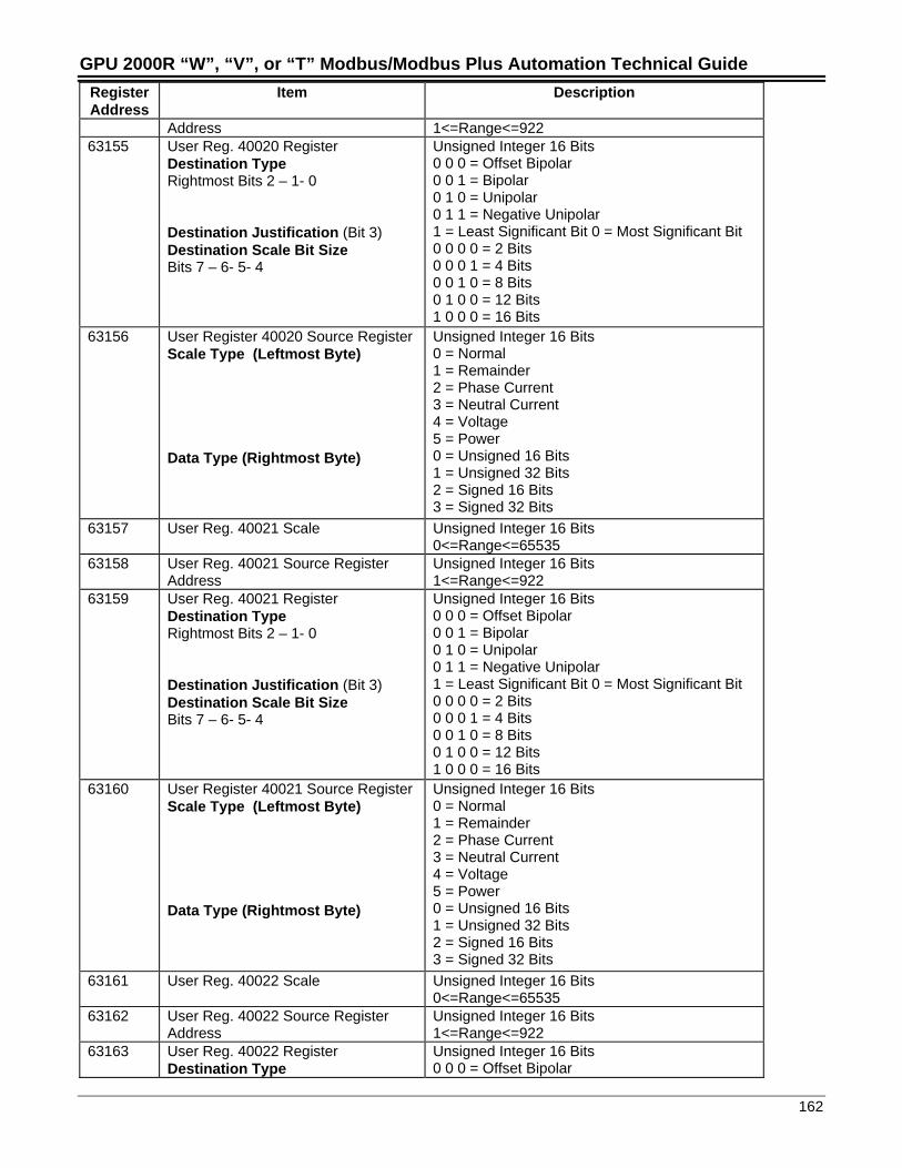
GPU 2000R “W”, “V”, or “T” Modbus/Modbus Plus Automation Technical Guide
162
RegisterAddress
Item Description
Address 1<=Range<=92263155 User Reg. 40020 Register
Destination TypeRightmost Bits 2 – 1- 0
Destination Justification (Bit 3)Destination Scale Bit SizeBits 7 – 6- 5- 4
Unsigned Integer 16 Bits0 0 0 = Offset Bipolar0 0 1 = Bipolar0 1 0 = Unipolar0 1 1 = Negative Unipolar1 = Least Significant Bit 0 = Most Significant Bit0 0 0 0 = 2 Bits0 0 0 1 = 4 Bits0 0 1 0 = 8 Bits0 1 0 0 = 12 Bits1 0 0 0 = 16 Bits
63156 User Register 40020 Source RegisterScale Type (Leftmost Byte)
Data Type (Rightmost Byte)
Unsigned Integer 16 Bits0 = Normal1 = Remainder2 = Phase Current3 = Neutral Current4 = Voltage5 = Power0 = Unsigned 16 Bits1 = Unsigned 32 Bits2 = Signed 16 Bits3 = Signed 32 Bits
63157 User Reg. 40021 Scale Unsigned Integer 16 Bits0<=Range<=65535
63158 User Reg. 40021 Source RegisterAddress
Unsigned Integer 16 Bits1<=Range<=922
63159 User Reg. 40021 RegisterDestination TypeRightmost Bits 2 – 1- 0
Destination Justification (Bit 3)Destination Scale Bit SizeBits 7 – 6- 5- 4
Unsigned Integer 16 Bits0 0 0 = Offset Bipolar0 0 1 = Bipolar0 1 0 = Unipolar0 1 1 = Negative Unipolar1 = Least Significant Bit 0 = Most Significant Bit0 0 0 0 = 2 Bits0 0 0 1 = 4 Bits0 0 1 0 = 8 Bits0 1 0 0 = 12 Bits1 0 0 0 = 16 Bits
63160 User Register 40021 Source RegisterScale Type (Leftmost Byte)
Data Type (Rightmost Byte)
Unsigned Integer 16 Bits0 = Normal1 = Remainder2 = Phase Current3 = Neutral Current4 = Voltage5 = Power0 = Unsigned 16 Bits1 = Unsigned 32 Bits2 = Signed 16 Bits3 = Signed 32 Bits
63161 User Reg. 40022 Scale Unsigned Integer 16 Bits0<=Range<=65535
63162 User Reg. 40022 Source RegisterAddress
Unsigned Integer 16 Bits1<=Range<=922
63163 User Reg. 40022 RegisterDestination Type
Unsigned Integer 16 Bits0 0 0 = Offset Bipolar
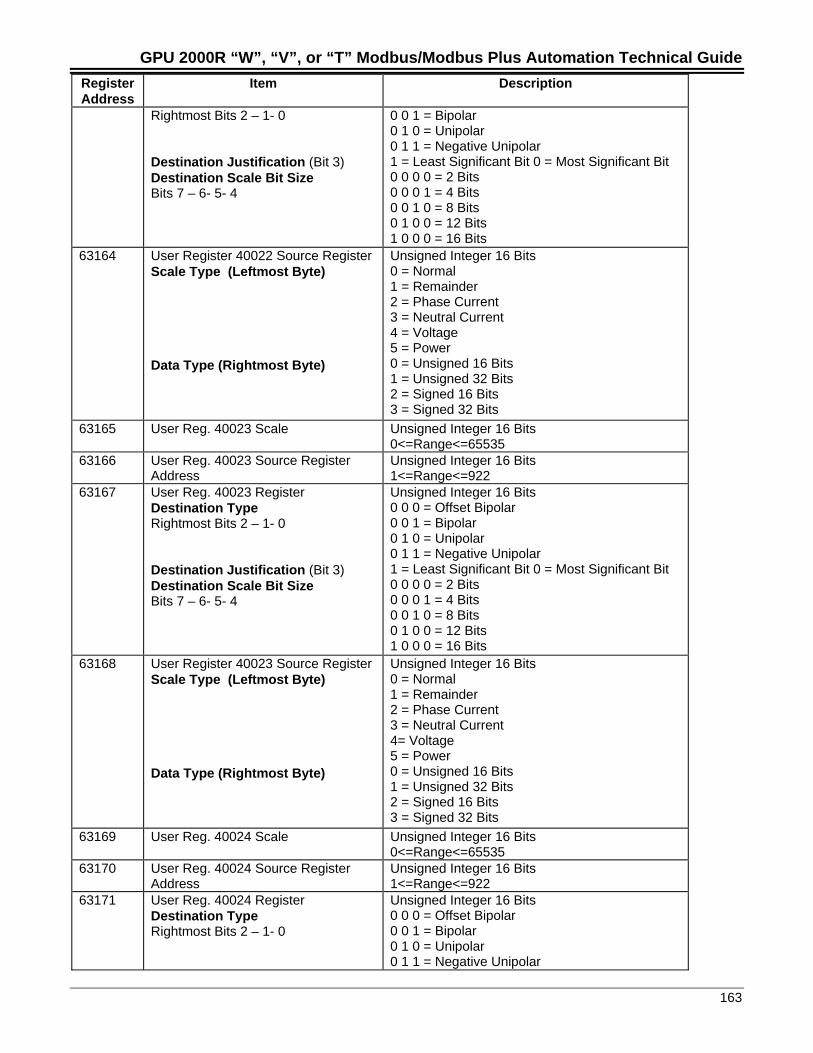
GPU 2000R “W”, “V”, or “T” Modbus/Modbus Plus Automation Technical Guide
163
RegisterAddress
Item Description
Rightmost Bits 2 – 1- 0
Destination Justification (Bit 3)Destination Scale Bit SizeBits 7 – 6- 5- 4
0 0 1 = Bipolar0 1 0 = Unipolar0 1 1 = Negative Unipolar1 = Least Significant Bit 0 = Most Significant Bit0 0 0 0 = 2 Bits0 0 0 1 = 4 Bits0 0 1 0 = 8 Bits0 1 0 0 = 12 Bits1 0 0 0 = 16 Bits
63164 User Register 40022 Source RegisterScale Type (Leftmost Byte)
Data Type (Rightmost Byte)
Unsigned Integer 16 Bits0 = Normal1 = Remainder2 = Phase Current3 = Neutral Current4 = Voltage5 = Power0 = Unsigned 16 Bits1 = Unsigned 32 Bits2 = Signed 16 Bits3 = Signed 32 Bits
63165 User Reg. 40023 Scale Unsigned Integer 16 Bits0<=Range<=65535
63166 User Reg. 40023 Source RegisterAddress
Unsigned Integer 16 Bits1<=Range<=922
63167 User Reg. 40023 RegisterDestination TypeRightmost Bits 2 – 1- 0
Destination Justification (Bit 3)Destination Scale Bit SizeBits 7 – 6- 5- 4
Unsigned Integer 16 Bits0 0 0 = Offset Bipolar0 0 1 = Bipolar0 1 0 = Unipolar0 1 1 = Negative Unipolar1 = Least Significant Bit 0 = Most Significant Bit0 0 0 0 = 2 Bits0 0 0 1 = 4 Bits0 0 1 0 = 8 Bits0 1 0 0 = 12 Bits1 0 0 0 = 16 Bits
63168 User Register 40023 Source RegisterScale Type (Leftmost Byte)
Data Type (Rightmost Byte)
Unsigned Integer 16 Bits0 = Normal1 = Remainder2 = Phase Current3 = Neutral Current4= Voltage5 = Power0 = Unsigned 16 Bits1 = Unsigned 32 Bits2 = Signed 16 Bits3 = Signed 32 Bits
63169 User Reg. 40024 Scale Unsigned Integer 16 Bits0<=Range<=65535
63170 User Reg. 40024 Source RegisterAddress
Unsigned Integer 16 Bits1<=Range<=922
63171 User Reg. 40024 RegisterDestination TypeRightmost Bits 2 – 1- 0
Unsigned Integer 16 Bits0 0 0 = Offset Bipolar0 0 1 = Bipolar0 1 0 = Unipolar0 1 1 = Negative Unipolar
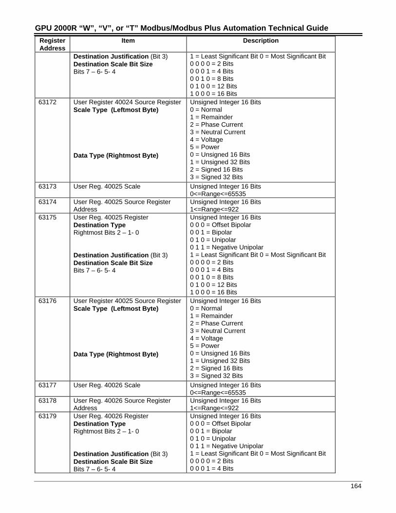
GPU 2000R “W”, “V”, or “T” Modbus/Modbus Plus Automation Technical Guide
164
RegisterAddress
Item Description
Destination Justification (Bit 3)Destination Scale Bit SizeBits 7 – 6- 5- 4
1 = Least Significant Bit 0 = Most Significant Bit0 0 0 0 = 2 Bits0 0 0 1 = 4 Bits0 0 1 0 = 8 Bits0 1 0 0 = 12 Bits1 0 0 0 = 16 Bits
63172 User Register 40024 Source RegisterScale Type (Leftmost Byte)
Data Type (Rightmost Byte)
Unsigned Integer 16 Bits0 = Normal1 = Remainder2 = Phase Current3 = Neutral Current4 = Voltage5 = Power0 = Unsigned 16 Bits1 = Unsigned 32 Bits2 = Signed 16 Bits3 = Signed 32 Bits
63173 User Reg. 40025 Scale Unsigned Integer 16 Bits0<=Range<=65535
63174 User Reg. 40025 Source RegisterAddress
Unsigned Integer 16 Bits1<=Range<=922
63175 User Reg. 40025 RegisterDestination TypeRightmost Bits 2 – 1- 0
Destination Justification (Bit 3)Destination Scale Bit SizeBits 7 – 6- 5- 4
Unsigned Integer 16 Bits0 0 0 = Offset Bipolar0 0 1 = Bipolar0 1 0 = Unipolar0 1 1 = Negative Unipolar1 = Least Significant Bit 0 = Most Significant Bit0 0 0 0 = 2 Bits0 0 0 1 = 4 Bits0 0 1 0 = 8 Bits0 1 0 0 = 12 Bits1 0 0 0 = 16 Bits
63176 User Register 40025 Source RegisterScale Type (Leftmost Byte)
Data Type (Rightmost Byte)
Unsigned Integer 16 Bits0 = Normal1 = Remainder2 = Phase Current3 = Neutral Current4 = Voltage5 = Power0 = Unsigned 16 Bits1 = Unsigned 32 Bits2 = Signed 16 Bits3 = Signed 32 Bits
63177 User Reg. 40026 Scale Unsigned Integer 16 Bits0<=Range<=65535
63178 User Reg. 40026 Source RegisterAddress
Unsigned Integer 16 Bits1<=Range<=922
63179 User Reg. 40026 RegisterDestination TypeRightmost Bits 2 – 1- 0
Destination Justification (Bit 3)Destination Scale Bit SizeBits 7 – 6- 5- 4
Unsigned Integer 16 Bits0 0 0 = Offset Bipolar0 0 1 = Bipolar0 1 0 = Unipolar0 1 1 = Negative Unipolar1 = Least Significant Bit 0 = Most Significant Bit0 0 0 0 = 2 Bits0 0 0 1 = 4 Bits
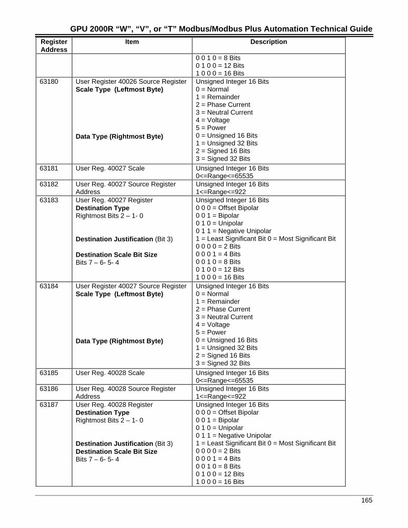
GPU 2000R “W”, “V”, or “T” Modbus/Modbus Plus Automation Technical Guide
165
RegisterAddress
Item Description
0 0 1 0 = 8 Bits0 1 0 0 = 12 Bits1 0 0 0 = 16 Bits
63180 User Register 40026 Source RegisterScale Type (Leftmost Byte)
Data Type (Rightmost Byte)
Unsigned Integer 16 Bits0 = Normal1 = Remainder2 = Phase Current3 = Neutral Current4 = Voltage5 = Power0 = Unsigned 16 Bits1 = Unsigned 32 Bits2 = Signed 16 Bits3 = Signed 32 Bits
63181 User Reg. 40027 Scale Unsigned Integer 16 Bits0<=Range<=65535
63182 User Reg. 40027 Source RegisterAddress
Unsigned Integer 16 Bits1<=Range<=922
63183 User Reg. 40027 RegisterDestination TypeRightmost Bits 2 – 1- 0
Destination Justification (Bit 3)
Destination Scale Bit SizeBits 7 – 6- 5- 4
Unsigned Integer 16 Bits0 0 0 = Offset Bipolar0 0 1 = Bipolar0 1 0 = Unipolar0 1 1 = Negative Unipolar1 = Least Significant Bit 0 = Most Significant Bit0 0 0 0 = 2 Bits0 0 0 1 = 4 Bits0 0 1 0 = 8 Bits0 1 0 0 = 12 Bits1 0 0 0 = 16 Bits
63184 User Register 40027 Source RegisterScale Type (Leftmost Byte)
Data Type (Rightmost Byte)
Unsigned Integer 16 Bits0 = Normal1 = Remainder2 = Phase Current3 = Neutral Current4 = Voltage5 = Power0 = Unsigned 16 Bits1 = Unsigned 32 Bits2 = Signed 16 Bits3 = Signed 32 Bits
63185 User Reg. 40028 Scale Unsigned Integer 16 Bits0<=Range<=65535
63186 User Reg. 40028 Source RegisterAddress
Unsigned Integer 16 Bits1<=Range<=922
63187 User Reg. 40028 RegisterDestination TypeRightmost Bits 2 – 1- 0
Destination Justification (Bit 3)Destination Scale Bit SizeBits 7 – 6- 5- 4
Unsigned Integer 16 Bits0 0 0 = Offset Bipolar0 0 1 = Bipolar0 1 0 = Unipolar0 1 1 = Negative Unipolar1 = Least Significant Bit 0 = Most Significant Bit0 0 0 0 = 2 Bits0 0 0 1 = 4 Bits0 0 1 0 = 8 Bits0 1 0 0 = 12 Bits1 0 0 0 = 16 Bits
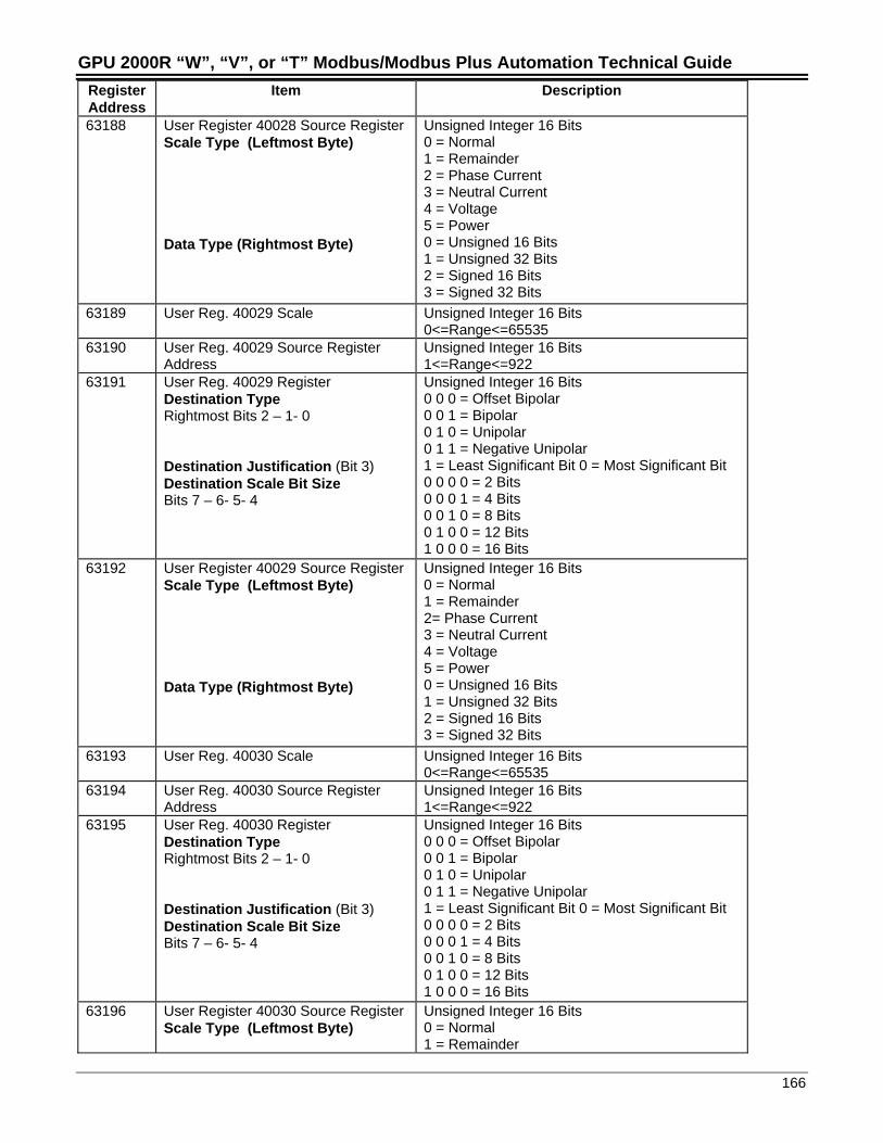
GPU 2000R “W”, “V”, or “T” Modbus/Modbus Plus Automation Technical Guide
166
RegisterAddress
Item Description
63188 User Register 40028 Source RegisterScale Type (Leftmost Byte)
Data Type (Rightmost Byte)
Unsigned Integer 16 Bits0 = Normal1 = Remainder2 = Phase Current3 = Neutral Current4 = Voltage5 = Power0 = Unsigned 16 Bits1 = Unsigned 32 Bits2 = Signed 16 Bits3 = Signed 32 Bits
63189 User Reg. 40029 Scale Unsigned Integer 16 Bits0<=Range<=65535
63190 User Reg. 40029 Source RegisterAddress
Unsigned Integer 16 Bits1<=Range<=922
63191 User Reg. 40029 RegisterDestination TypeRightmost Bits 2 – 1- 0
Destination Justification (Bit 3)Destination Scale Bit SizeBits 7 – 6- 5- 4
Unsigned Integer 16 Bits0 0 0 = Offset Bipolar0 0 1 = Bipolar0 1 0 = Unipolar0 1 1 = Negative Unipolar1 = Least Significant Bit 0 = Most Significant Bit0 0 0 0 = 2 Bits0 0 0 1 = 4 Bits0 0 1 0 = 8 Bits0 1 0 0 = 12 Bits1 0 0 0 = 16 Bits
63192 User Register 40029 Source RegisterScale Type (Leftmost Byte)
Data Type (Rightmost Byte)
Unsigned Integer 16 Bits0 = Normal1 = Remainder2= Phase Current3 = Neutral Current4 = Voltage5 = Power0 = Unsigned 16 Bits1 = Unsigned 32 Bits2 = Signed 16 Bits3 = Signed 32 Bits
63193 User Reg. 40030 Scale Unsigned Integer 16 Bits0<=Range<=65535
63194 User Reg. 40030 Source RegisterAddress
Unsigned Integer 16 Bits1<=Range<=922
63195 User Reg. 40030 RegisterDestination TypeRightmost Bits 2 – 1- 0
Destination Justification (Bit 3)Destination Scale Bit SizeBits 7 – 6- 5- 4
Unsigned Integer 16 Bits0 0 0 = Offset Bipolar0 0 1 = Bipolar0 1 0 = Unipolar0 1 1 = Negative Unipolar1 = Least Significant Bit 0 = Most Significant Bit0 0 0 0 = 2 Bits0 0 0 1 = 4 Bits0 0 1 0 = 8 Bits0 1 0 0 = 12 Bits1 0 0 0 = 16 Bits
63196 User Register 40030 Source RegisterScale Type (Leftmost Byte)
Unsigned Integer 16 Bits0 = Normal1 = Remainder
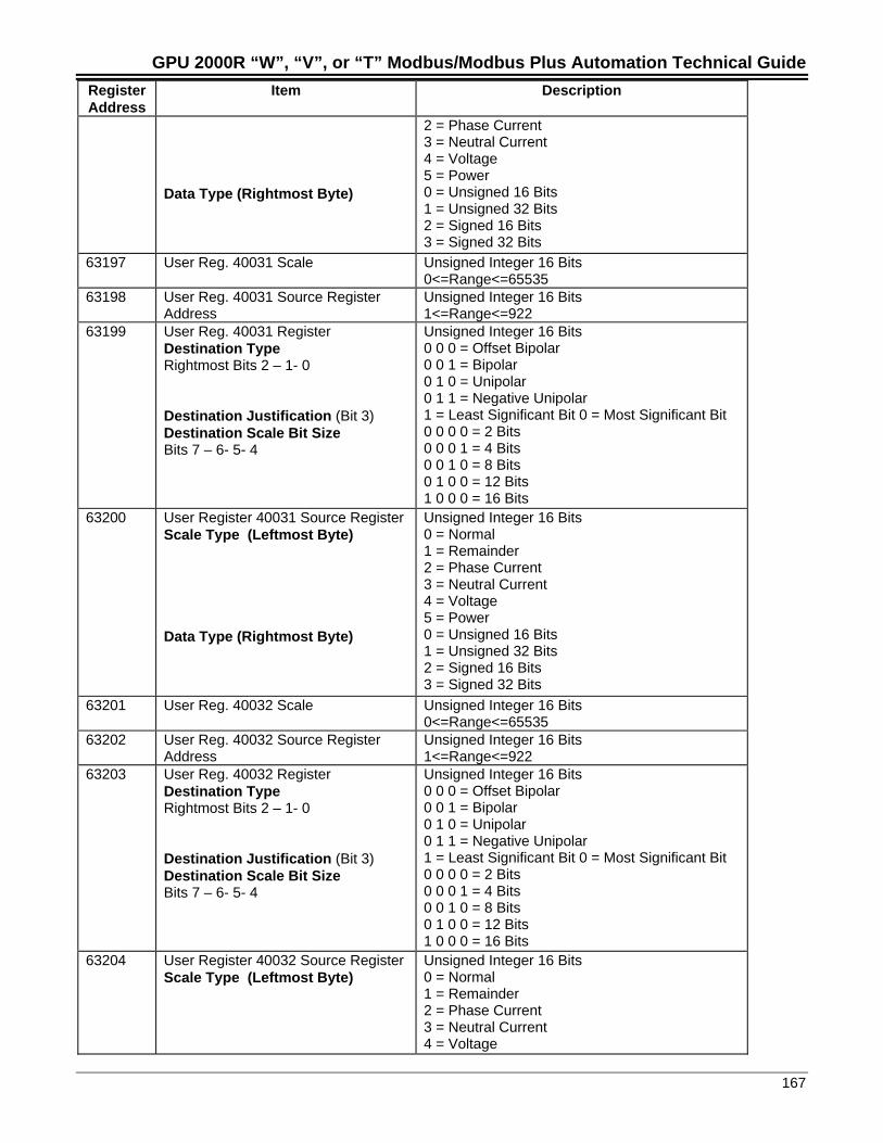
GPU 2000R “W”, “V”, or “T” Modbus/Modbus Plus Automation Technical Guide
167
RegisterAddress
Item Description
Data Type (Rightmost Byte)
2 = Phase Current3 = Neutral Current4 = Voltage5 = Power0 = Unsigned 16 Bits1 = Unsigned 32 Bits2 = Signed 16 Bits3 = Signed 32 Bits
63197 User Reg. 40031 Scale Unsigned Integer 16 Bits0<=Range<=65535
63198 User Reg. 40031 Source RegisterAddress
Unsigned Integer 16 Bits1<=Range<=922
63199 User Reg. 40031 RegisterDestination TypeRightmost Bits 2 – 1- 0
Destination Justification (Bit 3)Destination Scale Bit SizeBits 7 – 6- 5- 4
Unsigned Integer 16 Bits0 0 0 = Offset Bipolar0 0 1 = Bipolar0 1 0 = Unipolar0 1 1 = Negative Unipolar1 = Least Significant Bit 0 = Most Significant Bit0 0 0 0 = 2 Bits0 0 0 1 = 4 Bits0 0 1 0 = 8 Bits0 1 0 0 = 12 Bits1 0 0 0 = 16 Bits
63200 User Register 40031 Source RegisterScale Type (Leftmost Byte)
Data Type (Rightmost Byte)
Unsigned Integer 16 Bits0 = Normal1 = Remainder2 = Phase Current3 = Neutral Current4 = Voltage5 = Power0 = Unsigned 16 Bits1 = Unsigned 32 Bits2 = Signed 16 Bits3 = Signed 32 Bits
63201 User Reg. 40032 Scale Unsigned Integer 16 Bits0<=Range<=65535
63202 User Reg. 40032 Source RegisterAddress
Unsigned Integer 16 Bits1<=Range<=922
63203 User Reg. 40032 RegisterDestination TypeRightmost Bits 2 – 1- 0
Destination Justification (Bit 3)Destination Scale Bit SizeBits 7 – 6- 5- 4
Unsigned Integer 16 Bits0 0 0 = Offset Bipolar0 0 1 = Bipolar0 1 0 = Unipolar0 1 1 = Negative Unipolar1 = Least Significant Bit 0 = Most Significant Bit0 0 0 0 = 2 Bits0 0 0 1 = 4 Bits0 0 1 0 = 8 Bits0 1 0 0 = 12 Bits1 0 0 0 = 16 Bits
63204 User Register 40032 Source RegisterScale Type (Leftmost Byte)
Unsigned Integer 16 Bits0 = Normal1 = Remainder2 = Phase Current3 = Neutral Current4 = Voltage
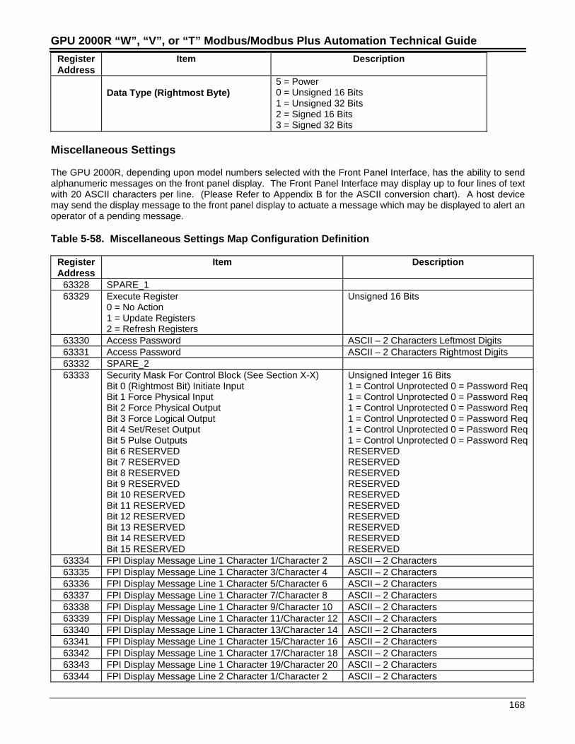
GPU 2000R “W”, “V”, or “T” Modbus/Modbus Plus Automation Technical Guide
168
RegisterAddress
Item Description
Data Type (Rightmost Byte)5 = Power0 = Unsigned 16 Bits1 = Unsigned 32 Bits2 = Signed 16 Bits3 = Signed 32 Bits
Miscellaneous Settings
The GPU 2000R, depending upon model numbers selected with the Front Panel Interface, has the ability to sendalphanumeric messages on the front panel display. The Front Panel Interface may display up to four lines of textwith 20 ASCII characters per line. (Please Refer to Appendix B for the ASCII conversion chart). A host devicemay send the display message to the front panel display to actuate a message which may be displayed to alert anoperator of a pending message.
Table 5-58. Miscellaneous Settings Map Configuration Definition
RegisterAddress
Item Description
63328 SPARE_163329 Execute Register
0 = No Action1 = Update Registers2 = Refresh Registers
Unsigned 16 Bits
63330 Access Password ASCII – 2 Characters Leftmost Digits63331 Access Password ASCII – 2 Characters Rightmost Digits63332 SPARE_263333 Security Mask For Control Block (See Section X-X)
Bit 0 (Rightmost Bit) Initiate InputBit 1 Force Physical InputBit 2 Force Physical OutputBit 3 Force Logical OutputBit 4 Set/Reset OutputBit 5 Pulse OutputsBit 6 RESERVEDBit 7 RESERVEDBit 8 RESERVEDBit 9 RESERVEDBit 10 RESERVEDBit 11 RESERVEDBit 12 RESERVEDBit 13 RESERVEDBit 14 RESERVEDBit 15 RESERVED
Unsigned Integer 16 Bits1 = Control Unprotected 0 = Password Req1 = Control Unprotected 0 = Password Req1 = Control Unprotected 0 = Password Req1 = Control Unprotected 0 = Password Req1 = Control Unprotected 0 = Password Req1 = Control Unprotected 0 = Password ReqRESERVEDRESERVEDRESERVEDRESERVEDRESERVEDRESERVEDRESERVEDRESERVEDRESERVEDRESERVED
63334 FPI Display Message Line 1 Character 1/Character 2 ASCII – 2 Characters63335 FPI Display Message Line 1 Character 3/Character 4 ASCII – 2 Characters63336 FPI Display Message Line 1 Character 5/Character 6 ASCII – 2 Characters63337 FPI Display Message Line 1 Character 7/Character 8 ASCII – 2 Characters63338 FPI Display Message Line 1 Character 9/Character 10 ASCII – 2 Characters63339 FPI Display Message Line 1 Character 11/Character 12 ASCII – 2 Characters63340 FPI Display Message Line 1 Character 13/Character 14 ASCII – 2 Characters63341 FPI Display Message Line 1 Character 15/Character 16 ASCII – 2 Characters63342 FPI Display Message Line 1 Character 17/Character 18 ASCII – 2 Characters63343 FPI Display Message Line 1 Character 19/Character 20 ASCII – 2 Characters63344 FPI Display Message Line 2 Character 1/Character 2 ASCII – 2 Characters
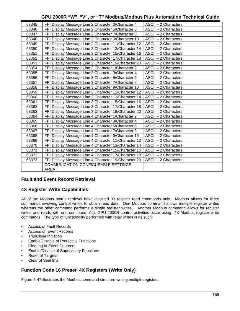
GPU 2000R “W”, “V”, or “T” Modbus/Modbus Plus Automation Technical Guide
169
63345 FPI Display Message Line 2 Character 3/Character 4 ASCII – 2 Characters63346 FPI Display Message Line 2 Character 5/Character 6 ASCII – 2 Characters63347 FPI Display Message Line 2 Character 7/Character 8 ASCII – 2 Characters63348 FPI Display Message Line 2 Character 9/Character 10 ASCII – 2 Characters63349 FPI Display Message Line 2 Character 11/Character 12 ASCII – 2 Characters63350 FPI Display Message Line 2 Character 13/Character 14 ASCII – 2 Characters63351 FPI Display Message Line 2 Character 15/Character 16 ASCII – 2 Characters63352 FPI Display Message Line 2 Character 17/Character 18 ASCII – 2 Characters63353 FPI Display Message Line 2 Character 19/Character 20 ASCII – 2 Characters63354 FPI Display Message Line 3 Character 1/Character 2 ASCII – 2 Characters63355 FPI Display Message Line 3 Character 3/Character 4 ASCII – 2 Characters63356 FPI Display Message Line 3 Character 5/Character 6 ASCII – 2 Characters63357 FPI Display Message Line 3 Character 7/Character 8 ASCII – 2 Characters63358 FPI Display Message Line 3 Character 9/Character 10 ASCII – 2 Characters63359 FPI Display Message Line 3 Character 11/Character 12 ASCII – 2 Characters63360 FPI Display Message Line 3 Character 13/Character 14 ASCII – 2 Characters63361 FPI Display Message Line 3 Character 15/Character 16 ASCII – 2 Characters63362 FPI Display Message Line 3 Character 17/Character 18 ASCII – 2 Characters63363 FPI Display Message Line 3 Character 19/Character 20 ASCII – 2 Characters63364 FPI Display Message Line 4 Character 1/Character 2 ASCII – 2 Characters63365 FPI Display Message Line 4 Character 3/Character 4 ASCII – 2 Characters63366 FPI Display Message Line 4 Character 5/Character 6 ASCII – 2 Characters63367 FPI Display Message Line 4 Character 7/Character 8 ASCII – 2 Characters63368 FPI Display Message Line 4 Character 9/Character 10 ASCII – 2 Characters63369 FPI Display Message Line 4 Character 11/Character 12 ASCII – 2 Characters63370 FPI Display Message Line 4 Character 13/Character 14 ASCII – 2 Characters63371 FPI Display Message Line 4 Character 15/Character 16 ASCII – 2 Characters63372 FPI Display Message Line 4 Character 17/Character 18 ASCII – 2 Characters63373 FPI Display Message Line 4 Character 19/Character 20 ASCII – 2 Characters
COMMUNICATION CONFIGURABLE SETTINGSAREA
Fault and Event Record Retrieval
4X Register Write Capabilities
All of the Modbus status retrieval have involved 03 register read commands only. Modbus allows for threecommands involving control writes to obtain read data. One Modbus command allows multiple register writeswhereas the other command performs a single register writes. Another Modbus command allows for registerwrites and reads with one command. ALL GPU 2000R control activities occur using 4X Modbus register writecommands. The type of functionality performed with relay writes is as such:
• Access of Fault Records• Access of Event Records• Trip/Close Initiation• Enable/Disable of Protective Functions• Clearing of Event Counters• Enable/Disable of Supervisory Functions• Reset of Targets• Clear of Seal In’s
Function Code 16 Preset 4X Registers (Write Only)
Figure 5-47 illustrates the Modbus command structure writing multiple registers.
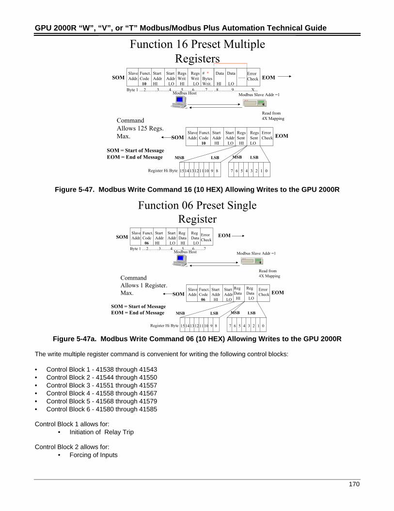
GPU 2000R “W”, “V”, or “T” Modbus/Modbus Plus Automation Technical Guide
170
Function 16 Preset MultipleRegisters
Modbus Host Modbus Slave Addr =1
Read from 4X Mapping
SlaveAddr.
Funct.Code 10
StartAddrHI
Start Addr LO
RegsWrit HI
RegsWrit LO
# *BytesWrit.
EOMSOM
SlaveAddr.
Funct.Code 10
StartAddr HI
StartAddr LO
RegsSent HI
RegsSentLO
ErrorCheck EOMSOM
Byte 1 …2……..3…….4…….5……6……..7…. ..8………9…………X...
MSB LSB
1514 1312 1110 9 8 7 6 5 4 3 2 1 0
MSB LSB
Register Hi Byte
Data
HI
Data
LO
ErrorCheck
CommandAllows 125 Regs.Max.
EC
SOM = Start of MessageEOM = End of Message
Figure 5-47. Modbus Write Command 16 (10 HEX) Allowing Writes to the GPU 2000R
Function 06 Preset SingleRegister
Modbus Host Modbus Slave Addr =1
Read from 4X Mapping
SlaveAddr.
Funct.Code 06
StartAddrHI
Start Addr LO
RegData HI
RegData LO
EOMSOM
SlaveAddr.
Funct.Code 06
StartAddr HI
StartAddr LO
ErrorCheck EOMSOM
Byte 1 …2……..3…….4…….5……6…….7
MSB LSB
151413 121110 9 8 7 6 5 4 3 2 1 0
MSB LSB
Register Hi Byte
ErrorCheck
CommandAllows 1 Register.Max.
EC
SOM = Start of MessageEOM = End of Message
RegData HI
RegData LO
Figure 5-47a. Modbus Write Command 06 (10 HEX) Allowing Writes to the GPU 2000R
The write multiple register command is convenient for writing the following control blocks:
• Control Block 1 - 41538 through 41543• Control Block 2 - 41544 through 41550• Control Block 3 - 41551 through 41557• Control Block 4 - 41558 through 41567• Control Block 5 - 41568 through 41579• Control Block 6 - 41580 through 41585
Control Block 1 allows for:• Initiation of Relay Trip
Control Block 2 allows for:• Forcing of Inputs
GPU 2000R “W”, “V”, or “T” Modbus/Modbus Plus Automation Technical Guide
171
Control Block 3 allows for:• Forcing of Outputs
Control Block 4 allows for:• Forcing of FLI Automation Bits
Control Block 5 allows for:• Reset of Latched Elements• Forcing of ULO Automation Bits
Control Block 6 allows for:• Pulse Control of Physical Outputs
Whenever a write occurs to the GPU 2000R:• The GPU 2000R receives the command:
• Command Interpreted in 1 quarter cycle.• Relay Protection Occurs.
• Command acts on the device.• The command response is generated to the Host from the GPU 2000R after the action is
completed.
Function 23 Read/Write Register (Read/Write Concurrently)
Another format command which allows for a simultaneous read/write is command 23 (17HEX). Figure 5-48illustrates the read/write 4X register command format. The 23 command is used when the user wishes to write aregister for control buffer access and read a group of registers which was accessed via the read.
Fault and operation records as well as the control groups allow for access of protective device function state. Ifa user wished to read the status of each function within the relay, a Function Read/Write Register Commandwould be the most desirable command to be issued. Read/Write register data commands are also useful inaccessing the Operation and Fault record blocks.
Review of the Modbus 23 command allows for write and read of data if the total amount of read and writeregisters do not exceed over 125 words. An advantage of using a combined read/write command is that ofspeed. If conventional commands were to be used, a 16 Write 4X Register Command would be issued andthereafter, within 10 seconds, a 03 Modbus (Read 4X Register Command) would then be issued to extract thedata from the relay. Using Modbus command 23 allows for decreasing of the overhead associated with multipleregister reads and writes.
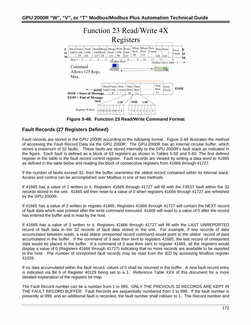
GPU 2000R “W”, “V”, or “T” Modbus/Modbus Plus Automation Technical Guide
172
Function 23 Read/Write 4XRegisters
Modbus Host
EC
Modbus Slave Addr =1
SlaveAddr.
Funct.Code 17
ReadAddrHI
Read Addr LO
#RegsRead HI
#RegsRead LO
Byte 1 …2……..3…….4…….5……6……..7…. ..8………9…..10……11……12………..X
Data
HI
Data
LO
ErrorCheck
CommandAllows 125 Regs.Max.
WriteAddr HI
WriteAddr LO
#RegsWrit. HI
#RegsWrit. LO
ByteCount *
SlaveAddr.
Funct.Code 17
ByteCount *
DataByte Hi
DataByte Lo
DataByte Lo
ErrorCheck EOMSOM
MSB LSB
151413 121110 9 8 7 6 5 4 3 2 1 0
MSB LSB
Register Hi Byte
SOM
EOM
SOM = Start of MessageEOM = End of Message
Figure 5-48. Function 23 Read/Write Command Format
Fault Records (27 Registers Defined)
Fault records are stored in the GPU 2000R according to the following format. Figure 5-49 illustrates the methodof accessing the Fault Record Data via the GPU 2000R. The GPU 2000R has an internal circular buffer, whichstores a maximum of 32 faults. These faults are stored internally to the GPU 2000R’s fault stack as indicated inthe figure. Each fault is defined as a block of 63 registers as shown in Tables 5-59 and 5-60. The first definedregister in the table is the fault record control register. Fault records are viewed by writing a data word to 41665as defined in the table below and reading the block of consecutive registers from 41666 through 41727.
If the number of faults exceed 32, then the buffer overwrites the oldest record contained within its internal stack.Access and control can be accomplished over Modbus in one of two methods.
If 41665 has a value of 1 written to it, Registers 41666 through 41727 will fill with the FIRST fault within the 32records stored in the unit. 41665 will then reset to a value of 0 when registers 41666 through 41727 are refreshedby the GPU 2000R.
If 41665 has a value of 2 written to register 41665, Registers 41666 through 41727 will contain the NEXT recordof fault data which was pointed after the write command executed. 41665 will reset to a value of 0 after the recordhas entered the buffer and is read by the host.
If 41665 has a value of 3 written to it, Registers 41666 through 41727 will fill with the LAST UNREPORTEDrecord of fault data in the 32 records of fault data stored in the unit. For example, if two records of dataaccumulated between reads, a read oldest unreported record command would point to the oldest record of dataaccumulated in the buffer. If the command of 3 was then sent to registers 41665, the last record of unreporteddata would be placed in the buffer. If a command of 3 was then sent to register 41665, all the registers woulddisplay a value of 0 (Registers 41666 through 41727) indicating that no more records are available to be reportedto the host. The number of unreported fault records may be read from the IED by accessing Modbus register41026.
If no data accumulated within the fault record, values of 0 shall be returned in the buffer. A new fault record entryis indicated via Bit 6 of Register 40129 being set to a 1. Reference Table XXX of this document for a moredetailed explanation of the registers bit map.
The Fault Record number can be a number from 1 to 999. ONLY THE PREVIOUS 32 RECORDS ARE KEPT INTHE FAULT RECORD BUFFER. Fault Records are sequentially numbered from 1 to 999. If the fault number ispresently at 999, and an additional fault is recorded, the fault number shall rollover to 1. The Record number and
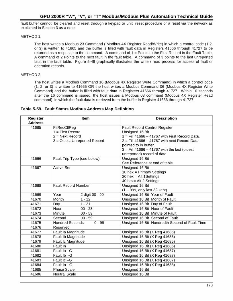
GPU 2000R “W”, “V”, or “T” Modbus/Modbus Plus Automation Technical Guide
173
fault buffer cannot be cleared and reset through a keypad or unit reset procedure or a reset via the network asexplained in Section 3 as a note.
METHOD 1:
The host writes a Modbus 23 Command ( Modbus 4X Register Read/Write) in which a control code (1,2,or 3) is written to 41665 and the buffer is filled with fault data in Registers 41666 through 41727 to bereturned as a response to the command. A command of 1 = Points to the First Record in the Fault Table.A command of 2 Points to the next fault in the fault table. A command of 3 points to the last unreportedfault in the fault table. Figure 5-49 graphically illustrates the write / read process for access of fault oroperation records.
METHOD 2:
The host writes a Modbus Command 16 (Modbus 4X Register Write Command) in which a control code(1, 2, or 3) is written to 41665 OR the host writes a Modbus Command 06 (Modbus 4X Register WriteCommand) and the buffer is filled with fault data in Registers 41666 through 41727. Within 10 secondsafter the 16 command is issued, the host issues a Modbus 03 command (Modbus 4X Register Readcommand) in which the fault data is retrieved from the buffer in Register 41666 through 41727.
Table 5-59. Fault Status Modbus Address Map Definition
RegisterAddress
Item Description
41665 FltRecCtlReg1 = First Record2 = Next Record3 = Oldest Unreported Record
Fault Record Control RegisterUnsigned 16 Bit1 = Fill 41666 – 41767 with First Record Data.2 = Fill 41666 – 41767 with next Record Datapointed to in buffer.3 = Fill 41666 – 41767 with the last (oldestunreported) record of data.
41666 Fault Trip Type (see below) Unsigned 16 BitSee Reference at end of table
41667 Active Set Unsigned 16 Bit10 hex = Primary Settings20 hex = Alt 1Settings40 hex= Alt 2 Settings
41668 Fault Record Number Unsigned 16 Bit(1 – 999, only last 32 kept)
41669 Year 2 digit 00 - 99 Unsigned 16 Bit Year of Fault41670 Month 1 - 12 Unsigned 16 Bit Month of Fault41671 Day 1 - 31 Unsigned 16 Bit Day of Fault41672 Hour 00 - 23 Unsigned 16 Bit Hour of Fault41673 Minute 00 - 59 Unsigned 16 Bit Minute of Fault41674 Second 00 - 59 Unsigned 16 Bit Second of Fault41675 Hundred Seconds 0 - 99 Unsigned 16 Bit Hundredth Second of Fault Time41676 Reserved41677 Fault Ia Magnitude Unsigned 16 Bit (X Reg 41685)41678 Fault Ib Magnitude Unsigned 16 Bit (X Reg 41685)41679 Fault Ic Magnitude Unsigned 16 Bit (X Reg 41685)41680 Fault In Unsigned 16 Bit (X Reg 41686)41681 Fault Ia –G Unsigned 16 Bit (X Reg 41687)41682 Fault Ib -G Unsigned 16 Bit (X Reg 41687)41683 Fault Ic –G Unsigned 16 Bit (X Reg 41687)41684 Fault In -G Unsigned 16 Bit (X Reg 41688)41685 Phase Scale Unsigned 16 Bit41686 Neutral Scale Unsigned 16 Bit
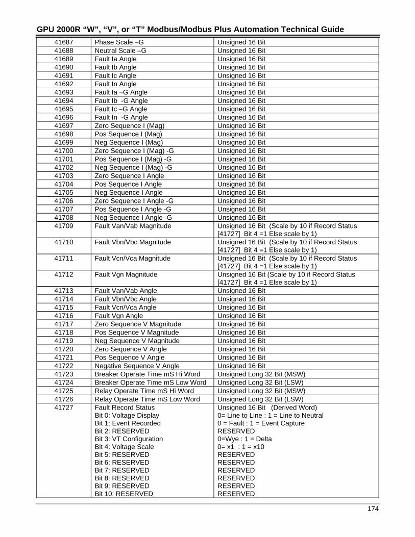
GPU 2000R “W”, “V”, or “T” Modbus/Modbus Plus Automation Technical Guide
174
41687 Phase Scale –G Unsigned 16 Bit41688 Neutral Scale –G Unsigned 16 Bit41689 Fault Ia Angle Unsigned 16 Bit41690 Fault Ib Angle Unsigned 16 Bit41691 Fault Ic Angle Unsigned 16 Bit41692 Fault In Angle Unsigned 16 Bit41693 Fault Ia –G Angle Unsigned 16 Bit41694 Fault Ib -G Angle Unsigned 16 Bit41695 Fault Ic –G Angle Unsigned 16 Bit41696 Fault In -G Angle Unsigned 16 Bit41697 Zero Sequence I (Mag) Unsigned 16 Bit41698 Pos Sequence I (Mag) Unsigned 16 Bit41699 Neg Sequence I (Mag) Unsigned 16 Bit41700 Zero Sequence I (Mag) -G Unsigned 16 Bit41701 Pos Sequence I (Mag) -G Unsigned 16 Bit41702 Neg Sequence I (Mag) -G Unsigned 16 Bit41703 Zero Sequence I Angle Unsigned 16 Bit41704 Pos Sequence I Angle Unsigned 16 Bit41705 Neg Sequence I Angle Unsigned 16 Bit41706 Zero Sequence I Angle -G Unsigned 16 Bit41707 Pos Sequence I Angle -G Unsigned 16 Bit41708 Neg Sequence I Angle -G Unsigned 16 Bit41709 Fault Van/Vab Magnitude Unsigned 16 Bit (Scale by 10 if Record Status
[41727] Bit 4 =1 Else scale by 1)41710 Fault Vbn/Vbc Magnitude Unsigned 16 Bit (Scale by 10 if Record Status
[41727] Bit 4 =1 Else scale by 1)41711 Fault Vcn/Vca Magnitude Unsigned 16 Bit (Scale by 10 if Record Status
[41727] Bit 4 =1 Else scale by 1)41712 Fault Vgn Magnitude Unsigned 16 Bit (Scale by 10 if Record Status
[41727] Bit 4 =1 Else scale by 1)41713 Fault Van/Vab Angle Unsigned 16 Bit41714 Fault Vbn/Vbc Angle Unsigned 16 Bit41715 Fault Vcn/Vca Angle Unsigned 16 Bit41716 Fault Vgn Angle Unsigned 16 Bit41717 Zero Sequence V Magnitude Unsigned 16 Bit41718 Pos Sequence V Magnitude Unsigned 16 Bit41719 Neg Sequence V Magnitude Unsigned 16 Bit41720 Zero Sequence V Angle Unsigned 16 Bit41721 Pos Sequence V Angle Unsigned 16 Bit41722 Negative Sequence V Angle Unsigned 16 Bit41723 Breaker Operate Time mS Hi Word Unsigned Long 32 Bit (MSW)41724 Breaker Operate Time mS Low Word Unsigned Long 32 Bit (LSW)41725 Relay Operate Time mS Hi Word Unsigned Long 32 Bit (MSW)41726 Relay Operate Time mS Low Word Unsigned Long 32 Bit (LSW)41727 Fault Record Status
Bit 0: Voltage DisplayBit 1: Event RecordedBit 2: RESERVEDBit 3: VT ConfigurationBit 4: Voltage ScaleBit 5: RESERVEDBit 6: RESERVEDBit 7: RESERVEDBit 8: RESERVEDBit 9: RESERVEDBit 10: RESERVED
Unsigned 16 Bit (Derived Word)0= Line to Line : 1 = Line to Neutral0 = Fault : 1 = Event CaptureRESERVED0=Wye : 1 = Delta0= x1 : 1 = x10RESERVEDRESERVEDRESERVEDRESERVEDRESERVEDRESERVED
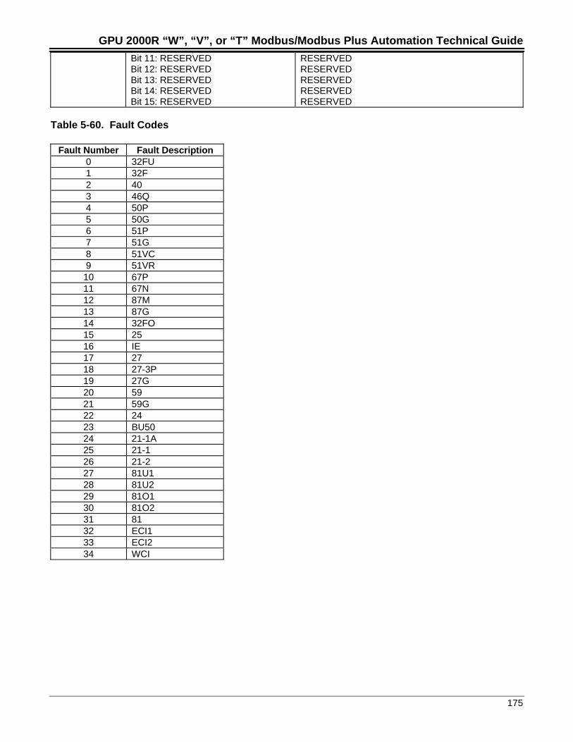
GPU 2000R “W”, “V”, or “T” Modbus/Modbus Plus Automation Technical Guide
175
Bit 11: RESERVEDBit 12: RESERVEDBit 13: RESERVEDBit 14: RESERVEDBit 15: RESERVED
RESERVEDRESERVEDRESERVEDRESERVEDRESERVED
Table 5-60. Fault Codes
Fault Number Fault Description0 32FU1 32F2 403 46Q4 50P5 50G6 51P7 51G8 51VC9 51VR10 67P11 67N12 87M13 87G14 32FO15 2516 IE17 2718 27-3P19 27G20 5921 59G22 2423 BU5024 21-1A25 21-126 21-227 81U128 81U229 81O130 81O231 8132 ECI133 ECI234 WCI
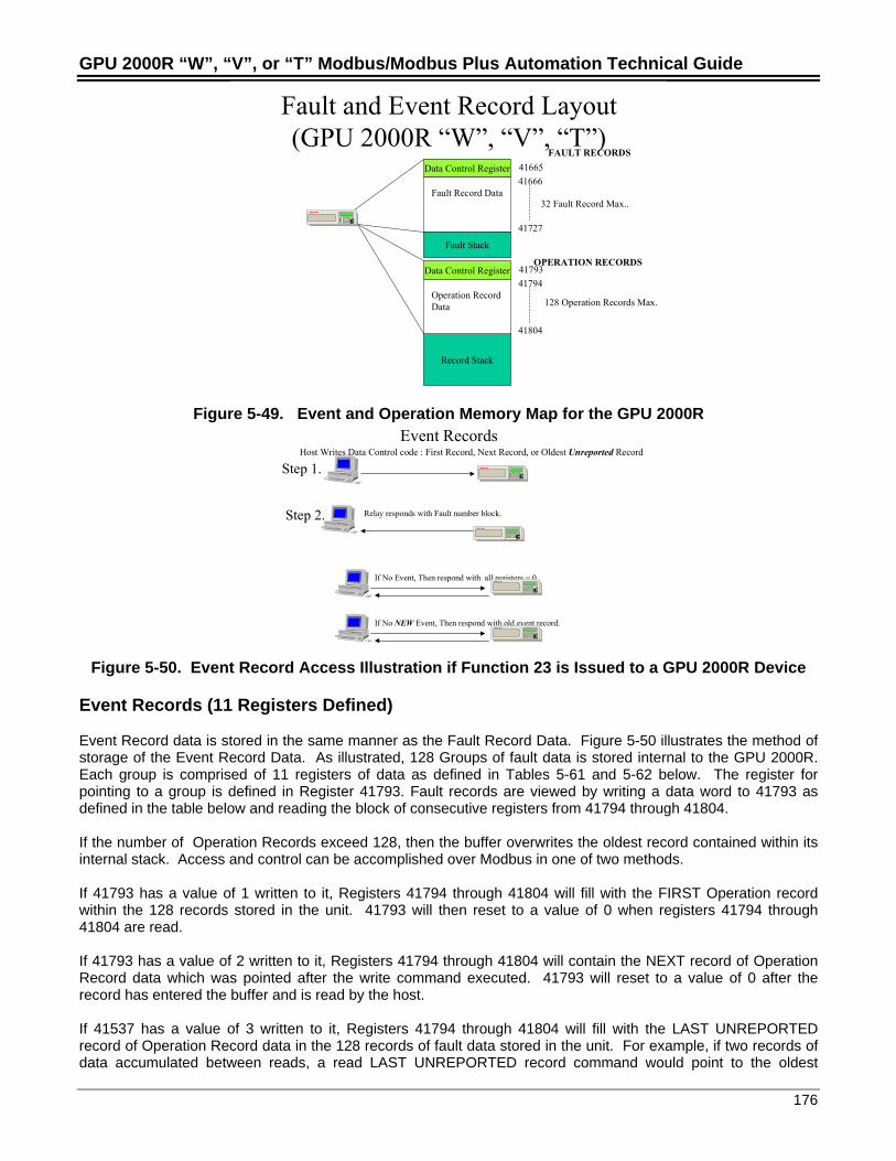
GPU 2000R “W”, “V”, or “T” Modbus/Modbus Plus Automation Technical Guide
176
Fault and Event Record Layout(GPU 2000R “W”, “V”, “T”)
Data Control Register
Fault Record Data
4166541666
41727
FAULT RECORDS
Data Control Register
Operation RecordData
4179341794
41804
32 Fault Record Max..
128 Operation Records Max.
Fault Stack
Record Stack
OPERATION RECORDS
EC
Figure 5-49. Event and Operation Memory Map for the GPU 2000REvent Records
Step 1.
Step 2.
Host Writes Data Control code : First Record, Next Record, or Oldest Unreported Record
Relay responds with Fault number block.
If No Event, Then respond with all registers = 0
If No NEW Event, Then respond with old event record.
EC
EC
EC
EC
Figure 5-50. Event Record Access Illustration if Function 23 is Issued to a GPU 2000R Device
Event Records (11 Registers Defined)
Event Record data is stored in the same manner as the Fault Record Data. Figure 5-50 illustrates the method ofstorage of the Event Record Data. As illustrated, 128 Groups of fault data is stored internal to the GPU 2000R.Each group is comprised of 11 registers of data as defined in Tables 5-61 and 5-62 below. The register forpointing to a group is defined in Register 41793. Fault records are viewed by writing a data word to 41793 asdefined in the table below and reading the block of consecutive registers from 41794 through 41804.
If the number of Operation Records exceed 128, then the buffer overwrites the oldest record contained within itsinternal stack. Access and control can be accomplished over Modbus in one of two methods.
If 41793 has a value of 1 written to it, Registers 41794 through 41804 will fill with the FIRST Operation recordwithin the 128 records stored in the unit. 41793 will then reset to a value of 0 when registers 41794 through41804 are read.
If 41793 has a value of 2 written to it, Registers 41794 through 41804 will contain the NEXT record of OperationRecord data which was pointed after the write command executed. 41793 will reset to a value of 0 after therecord has entered the buffer and is read by the host.
If 41537 has a value of 3 written to it, Registers 41794 through 41804 will fill with the LAST UNREPORTEDrecord of Operation Record data in the 128 records of fault data stored in the unit. For example, if two records ofdata accumulated between reads, a read LAST UNREPORTED record command would point to the oldest
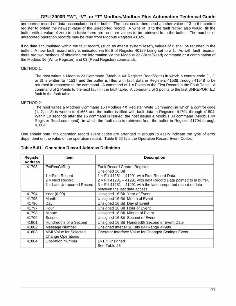
GPU 2000R “W”, “V”, or “T” Modbus/Modbus Plus Automation Technical Guide
177
unreported record of data accumulated in the buffer The host could then send another value of 3 to the controlregister to obtain the newest value of the unreported record. A write of 3 to the fault record also would fill thebuffer with a value of zero to indicate there are no other values to be retrieved from the buffer. The number ofunreported operation records may be read from Modbus Register 41025.
If no data accumulated within the fault record, (such as after a system reset), values of 0 shall be returned in thebuffer. A new fault record entry is indicated via Bit 8 of Register 40129 being set to a 1. As with fault records,there are two methods of obtaining the information via the Modbus 23 (Write/Read) command or a combination ofthe Modbus 16 (Write Register) and 03 (Read Register) commands.
METHOD 1:
The host writes a Modbus 23 Command (Modbus 4X Register Read/Write) in which a control code (1, 2,or 3) is written to 41537 and the buffer is filled with fault data in Registers 41538 through 41548 to bereturned in response to the command. A command of 1 = Points to the First Record in the Fault Table. Acommand of 2 Points to the next fault in the fault table. A command of 3 points to the last UNREPORTEDfault in the fault table.
METHOD 2:The host writes a Modbus Command 16 (Modbus 4X Register Write Command) in which a control code(1, 2, or 3) is written to 41665 and the buffer is filled with fault data in Registers 41794 through 41804.Within 10 seconds after the 16 command is issued, the host issues a Modbus 03 command (Modbus 4XRegister Read command) in which the fault data is retrieved from the buffer in Register 41794 through41804.
One should note the operation record event codes are arranged in groups to easily indicate the type of errordependent on the value of the operation record. Table 5-62 lists the Operation Record Event Codes.
Table 5-61. Operation Record Address Definition
RegisterAddress
Item Description
41793 EvtRecCtlReg
1 = First Record2 = Next Record3 = Last Unreported Record
Fault Record Control RegisterUnsigned 16 Bit1 = Fill 41281 – 41291 with First Record Data.2 = Fill 41281 – 41291 with next Record Data pointed to in buffer.3 = Fill 41281 – 41291 with the last unreported record of databetween the last data access
41794 Year (0-99) Unsigned 16 Bit Year of Event41795 Month Unsigned 16 Bit Month of Event41796 Day Unsigned 16 Bit Day of Event41797 Hour Unsigned 16 Bit Hour of Event41798 Minute Unsigned 16 Bit Minute of Event41799 Second Unsigned 16 Bit Second of Event41801 Hundredths of a Second Unsigned 16 Bit Hundredth Second of Event Date41802 Message Number Unsigned Integer 16 Bits 0<=Range <=99941803 MMI Value for Selected
Change OperationsOperator Interface Value for Changed Settings Event
41804 Operation Number 16 Bit UnsignedSee Table 25
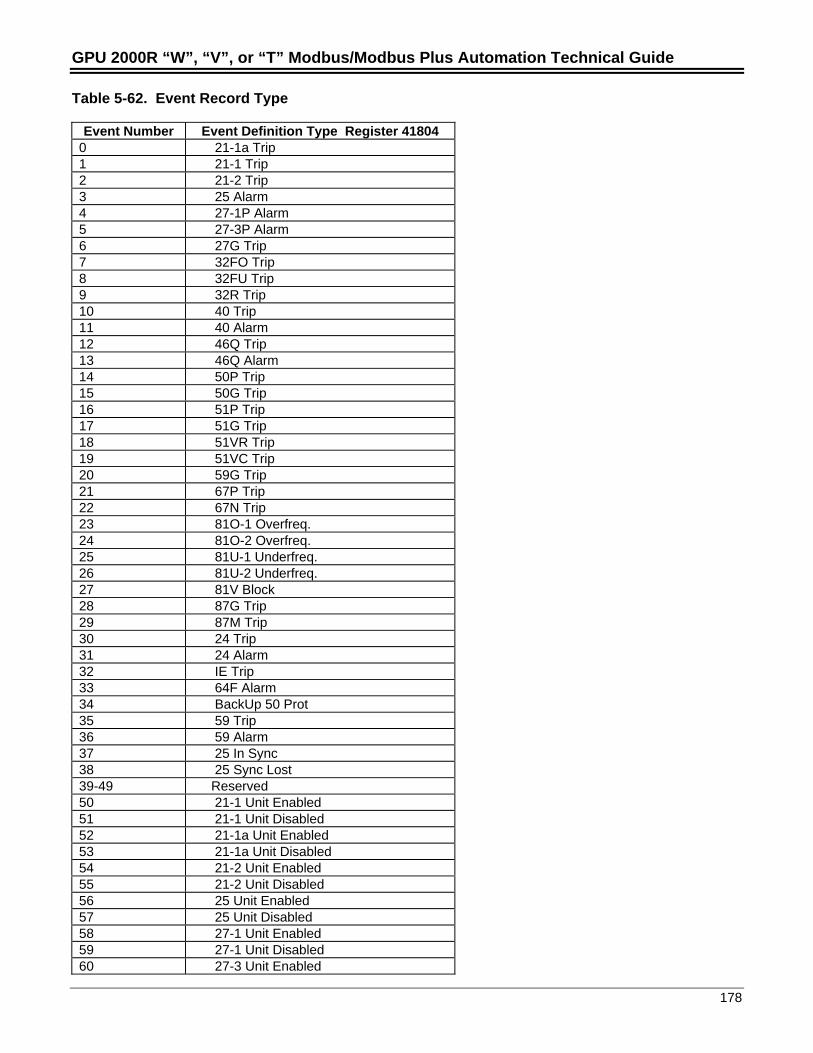
GPU 2000R “W”, “V”, or “T” Modbus/Modbus Plus Automation Technical Guide
178
Table 5-62. Event Record Type
Event Number Event Definition Type Register 418040 21-1a Trip1 21-1 Trip2 21-2 Trip3 25 Alarm4 27-1P Alarm5 27-3P Alarm6 27G Trip7 32FO Trip8 32FU Trip9 32R Trip10 40 Trip11 40 Alarm12 46Q Trip13 46Q Alarm14 50P Trip15 50G Trip16 51P Trip17 51G Trip18 51VR Trip19 51VC Trip20 59G Trip21 67P Trip22 67N Trip23 81O-1 Overfreq.24 81O-2 Overfreq.25 81U-1 Underfreq.26 81U-2 Underfreq.27 81V Block28 87G Trip29 87M Trip30 24 Trip31 24 Alarm32 IE Trip33 64F Alarm 34 BackUp 50 Prot35 59 Trip36 59 Alarm37 25 In Sync38 25 Sync Lost39-49 Reserved50 21-1 Unit Enabled51 21-1 Unit Disabled52 21-1a Unit Enabled53 21-1a Unit Disabled54 21-2 Unit Enabled55 21-2 Unit Disabled56 25 Unit Enabled57 25 Unit Disabled58 27-1 Unit Enabled59 27-1 Unit Disabled60 27-3 Unit Enabled
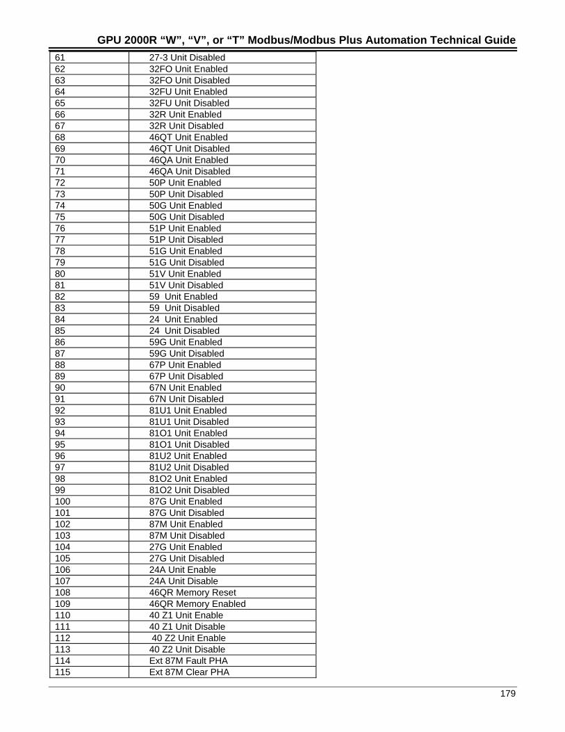
GPU 2000R “W”, “V”, or “T” Modbus/Modbus Plus Automation Technical Guide
179
61 27-3 Unit Disabled62 32FO Unit Enabled63 32FO Unit Disabled64 32FU Unit Enabled65 32FU Unit Disabled66 32R Unit Enabled67 32R Unit Disabled68 46QT Unit Enabled69 46QT Unit Disabled70 46QA Unit Enabled71 46QA Unit Disabled72 50P Unit Enabled73 50P Unit Disabled74 50G Unit Enabled75 50G Unit Disabled76 51P Unit Enabled77 51P Unit Disabled78 51G Unit Enabled79 51G Unit Disabled80 51V Unit Enabled81 51V Unit Disabled82 59 Unit Enabled83 59 Unit Disabled84 24 Unit Enabled85 24 Unit Disabled86 59G Unit Enabled87 59G Unit Disabled88 67P Unit Enabled89 67P Unit Disabled90 67N Unit Enabled91 67N Unit Disabled92 81U1 Unit Enabled93 81U1 Unit Disabled94 81O1 Unit Enabled95 81O1 Unit Disabled96 81U2 Unit Enabled97 81U2 Unit Disabled98 81O2 Unit Enabled99 81O2 Unit Disabled100 87G Unit Enabled101 87G Unit Disabled102 87M Unit Enabled103 87M Unit Disabled104 27G Unit Enabled105 27G Unit Disabled106 24A Unit Enable107 24A Unit Disable108 46QR Memory Reset109 46QR Memory Enabled110 40 Z1 Unit Enable111 40 Z1 Unit Disable112 40 Z2 Unit Enable113 40 Z2 Unit Disable114 Ext 87M Fault PHA115 Ext 87M Clear PHA
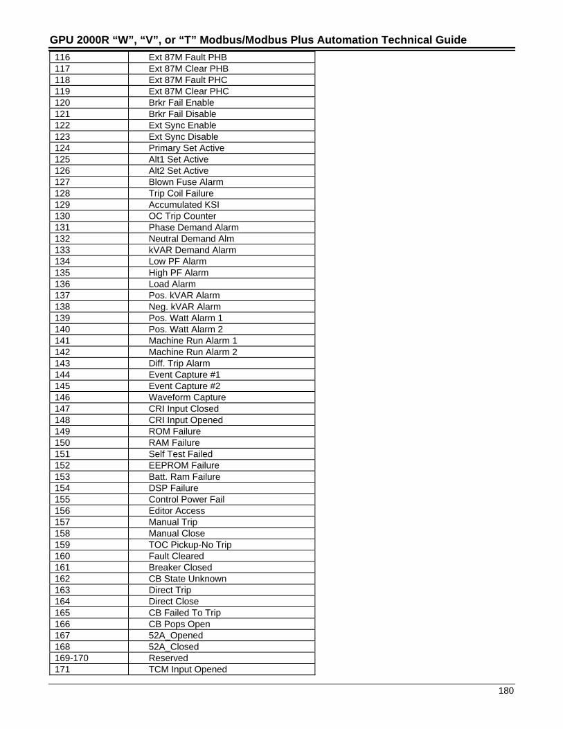
GPU 2000R “W”, “V”, or “T” Modbus/Modbus Plus Automation Technical Guide
180
116 Ext 87M Fault PHB117 Ext 87M Clear PHB118 Ext 87M Fault PHC119 Ext 87M Clear PHC120 Brkr Fail Enable121 Brkr Fail Disable122 Ext Sync Enable123 Ext Sync Disable124 Primary Set Active125 Alt1 Set Active126 Alt2 Set Active127 Blown Fuse Alarm128 Trip Coil Failure129 Accumulated KSI130 OC Trip Counter131 Phase Demand Alarm132 Neutral Demand Alm133 kVAR Demand Alarm134 Low PF Alarm135 High PF Alarm136 Load Alarm137 Pos. kVAR Alarm138 Neg. kVAR Alarm139 Pos. Watt Alarm 1140 Pos. Watt Alarm 2141 Machine Run Alarm 1142 Machine Run Alarm 2143 Diff. Trip Alarm144 Event Capture #1145 Event Capture #2146 Waveform Capture147 CRI Input Closed148 CRI Input Opened149 ROM Failure150 RAM Failure151 Self Test Failed152 EEPROM Failure153 Batt. Ram Failure154 DSP Failure155 Control Power Fail156 Editor Access157 Manual Trip158 Manual Close159 TOC Pickup-No Trip160 Fault Cleared161 Breaker Closed162 CB State Unknown163 Direct Trip164 Direct Close165 CB Failed To Trip166 CB Pops Open167 52A_Opened168 52A_Closed169-170 Reserved171 TCM Input Opened
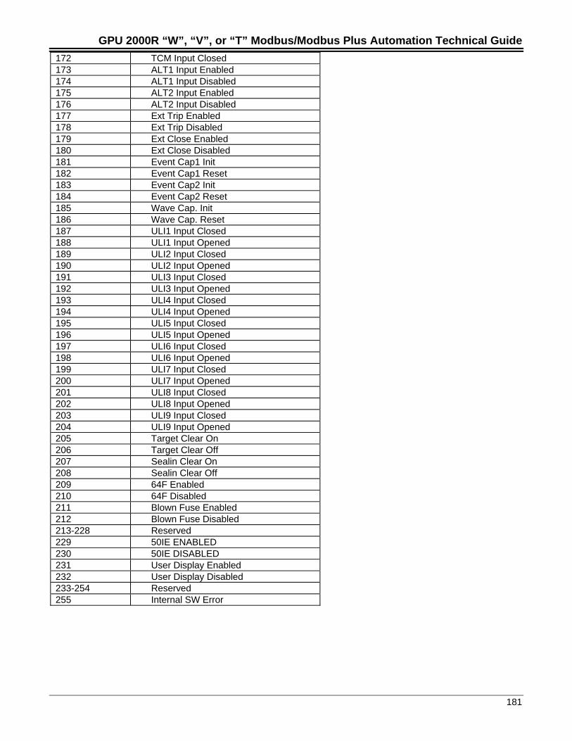
GPU 2000R “W”, “V”, or “T” Modbus/Modbus Plus Automation Technical Guide
181
172 TCM Input Closed173 ALT1 Input Enabled174 ALT1 Input Disabled175 ALT2 Input Enabled176 ALT2 Input Disabled177 Ext Trip Enabled178 Ext Trip Disabled179 Ext Close Enabled180 Ext Close Disabled181 Event Cap1 Init182 Event Cap1 Reset183 Event Cap2 Init184 Event Cap2 Reset185 Wave Cap. Init186 Wave Cap. Reset187 ULI1 Input Closed188 ULI1 Input Opened189 ULI2 Input Closed190 ULI2 Input Opened191 ULI3 Input Closed192 ULI3 Input Opened193 ULI4 Input Closed194 ULI4 Input Opened195 ULI5 Input Closed196 ULI5 Input Opened197 ULI6 Input Closed198 ULI6 Input Opened199 ULI7 Input Closed200 ULI7 Input Opened201 ULI8 Input Closed202 ULI8 Input Opened203 ULI9 Input Closed204 ULI9 Input Opened205 Target Clear On206 Target Clear Off207 Sealin Clear On208 Sealin Clear Off209 64F Enabled210 64F Disabled211 Blown Fuse Enabled212 Blown Fuse Disabled213-228 Reserved229 50IE ENABLED230 50IE DISABLED231 User Display Enabled232 User Display Disabled233-254 Reserved255 Internal SW Error
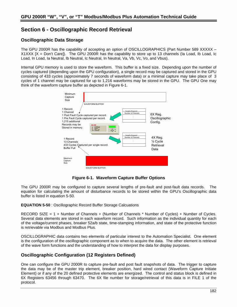
GPU 2000R “W”, “V”, or “T” Modbus/Modbus Plus Automation Technical Guide
182
Section 6 - Oscillographic Record Retrieval
Oscillographic Data Storage
The GPU 2000R has the capability of accepting an option of OSCILLOGRAPHICS (Part Number 589 XXXXX –X1XXX [X = Don’t Care]). The GPU 2000R has the capability to store up to 13 channels (Ia Load, Ib Load, IcLoad, In Load, Ia Neutral, Ib Neutral, Ic Neutral, In Neutral, Va, Vb, Vc, Vo, and Vbus).
Internal GPU memory is used to store the waveform. This buffer is a fixed size. Depending upon the number ofcycles captured (depending upon the GPU configuration), a single record may be captured and stored in the GPUconsisting of 433 cycles (approximately 7 seconds of waveform data) or a minimal capture may take place of 3cycles of 1 channel may be captured for up to 1,216 waveforms may be stored in the GPU. The GPU One maythink of the waveform capture buffer as depicted in Figure 6-1.
MinimumCapture Size
WAVEFORM BUFFER
WAVEFORM BUFFER
Maximum Capture Size
E
C
ABCNRST
XX XXXXX XXXX XX XXXXXXXXXXX XXXX XXXXX XXXXXXX
STATUS TARGETS
6X Reg.OscillographicConfig.
Samples RequiredNumber of Channels
Samples RequiredNumber of Channels 4X Reg.
¼ CycleRetrievalData
1 Record.1 Channel1 Post Fault Cycle captured per record.1 Pre Fault Cycle captured per record.1,215 additionalRecords may beStored in memory.
1 Record13 Channels433 Cycles Captured per single record.Buffer Full
Figure 6-1. Waveform Capture Buffer Options
The GPU 2000R may be configured to capture several lengths of pre-fault and post-fault data records. Theequation for calculating the amount of disturbance records to be stored within the GPU’s Oscillographic databuffer is listed in equation 5-50.
EQUATION 5-50 : Oscillographic Record Buffer Storage Calcuations
RECORD SIZE = 1 + Number of Channels + (Number of Channels * Number of Cycles) + Number of Cycles.Several data elements are stored in each waveform record. Such information as the individual quantity for eachof the voltage/current phases, breaker 52a/b state, time-stamping information, and state of the protective functionis retrievable via Modbus and Modbus Plus.
OSCILLOGRAPHIC data contains two elements of particular interest to the Automation Specialist. One elementis the configuration of the oscillographic component as to when to acquire the data. The other element is retrievalof the wave form functions and the understanding of how to interpret the data for display purposes.
Oscillographic Configuration (12 Registers Defined)
One can configure the GPU 2000R to capture pre-fault and post fault snapshots of data. The trigger to capturethe data may be of the master trip element, breaker position, hard wired contact (Waveform Capture InitiateElement) or if any of the 20 defined protective elements are energized. The control and status block is defined in6X Registers 63456 through 63470. The 6X file number for storage/retrieval of this data is in FILE 1 of theprotocol.
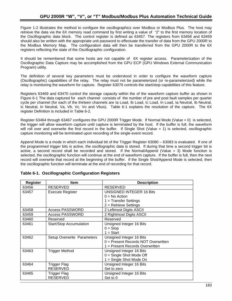
GPU 2000R “W”, “V”, or “T” Modbus/Modbus Plus Automation Technical Guide
183
Figure 1-2 illustrates the method to configure the oscillographics over Modbus or Modbus Plus. The host mayretrieve the data via the 6X memory read command by first writing a value of “2” to the first memory location ofthe Oscillographic data block. The control register is defined as 63457. The registers from 63458 and 63459should also be written with the appropriate unit password to effectuate the transfer of data from the GPU 2000R tothe Modbus Memory Map. The configuration data will then be transferred from the GPU 2000R to the 6Xregisters reflecting the state of the Oscillographic configuration.
It should be remembered that some hosts are not capable of 6X register access. Parameterization of theOscillographic Data Capture may be accomplished from the GPU ECP (GPU Windows External CommunicationProgram) utility.
The definition of several key parameters must be understood in order to configure the waveform capture(Oscillographic) capabilities of the relay. The relay must not be parameterized (or re-parameterized) while therelay is monitoring the waveform for capture. Register 63076 controls the start/stop capabilities of this feature.
Registers 63469 and 63470 control the storage capacity within the of the waveform capture buffer as shown inFigure 6-1 The data captured for each channel consists of the number of pre and post fault samples per quartercycle per channel (for each of the thirteen channels are Ia Load, Ib Load, Ic Load, In Load, Ia Neutral, Ib Neutral,Ic Neutral, In Neutral, Va, Vb, Vc, Vo and Vbus). Table 6-1 explains the resolution of the capture. The 6Xregister Definition is included in Table 6-2.
Register 63464 through 63467 configures the GPU 2000R Trigger Mode. If Normal Mode (Value = 0) is selected,the trigger will allow waveform capture until capture is terminated by the host. If the buffer is full, the waveformwill roll over and overwrite the first record in the buffer. If Single Shot (Value = 1) is selected, oscillographiccapture monitoring will be terminated upon recording of the single event record.
Append Mode is a mode in which each individual bit of the Trigger Register 63080 – 63083 is evaluated. If one ofthe programmed trigger bits is active, the oscillographic data is stored. If during that time a second trigger bit isactive, a second record shall be recorded and stored. If the Normal/Append (Value = 3) Mode function isselected, the oscillographic function will continue at the end of waveform capture. If the buffer is full, then the nextrecord will overwrite that record at the beginning of the buffer. If the Single Shot/Append Mode is selected, thenthe oscillographic function will terminate at the end of recording for that record.
Table 6-1. Oscillographic Configuration Registers
Register Item Description63456 RESERVED RESERVED63457 Execute Register UNSIGNED INTEGER 16 Bits
0 = No Action1 = Transfer Settings2 = Retrieve Settings
63458 Access PASSWORD 2 Leftmost Digits ASCII63459 Access PASSWORD 2 Rightmost Digits ASCII63460 Reserved Reserved63461 Start/Stop Accumulation Unsigned Integer 16 Bits
0 = Stop1 = Start
63462 Setup Overwrite Parameters Unsigned Integer 16 Bits0 = Present Records NOT Overwritten1 = Present Records Overwritten
63463 Trigger Method Unsigned Integer 16 Bits0 = Single Shot Mode Off1 = Single Shot Mode On
63464 Trigger FlagRESERVED
Unsigned Integer 16 BitsSet to zero
63465 Trigger FlagRESERVED
Unsigned Integer 16 BitsSet to 0
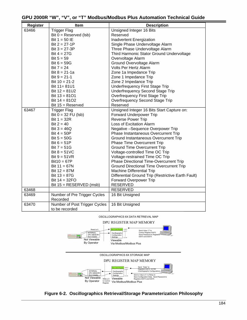
GPU 2000R “W”, “V”, or “T” Modbus/Modbus Plus Automation Technical Guide
184
Register Item Description63466 Trigger Flag
Bit 0 = Reserved (lsb)Bit 1 = 50 IEBit 2 = 27-1PBit 3 = 27-3PBit 4 = 27GBit 5 = 59Bit 6 = 59GBit 7 = 24Bit 8 = 21-1aBit 9 = 21-1Bit 10 = 21-2Bit 11= 81U1Bit 12 = 81U2Bit 13 = 81O1Bit 14 = 81O2Bit 15 = Reserved
Unsigned Integer 16 BitsReservedInadvertent EnergizationSingle Phase Undervoltage AlarmThree Phase Undervoltage AlarmThird Harmonic Stator Ground UndervoltageOvervoltage AlarmGround Overvoltage AlarmVolts Per Hertz AlarmZone 1a Impedance TripZone 1 Impedance TripZone 2 Impedance TripUnderfrequency First Stage TripUnderfrequency Second Stage TripOverfrequency First Stage TripOverfrequency Second Stage TripReserved
63467 Trigger FlagBit 0 = 32 FU (lsb)Bit 1 = 32RBit 2 = 40Bit 3 = 46QBit 4 = 50PBit 5 = 50GBit 6 = 51PBit 7 = 51GBit 8 = 51VCBit 9 = 51VRBit10 = 67PBit 11 = 67NBit 12 = 87MBit 13 = 87GBit 14 = 32FOBit 15 = RESERVED (msb)
Unsigned Integer 16 Bits Start Capture on:Forward Underpower TripReverse Power TripLoss of Excitation AlarmNegative –Sequence Overpower TripPhase Instantaneous Overcurrent TripGround Instantaneous Overcurrent TripPhase Time Overcurrent TripGround Time Overcurrent TripVoltage-controlled Time OC TripVoltage-restrained Time OC TripPhase Directional Time-Overcurrent TripGround Directional Time Overcurrent TripMachine Differential TripDifferential Ground Trip (Restrictive Earth Fault)Forward Overpower TripRESERVED
63468 RESERVED63469 Number of Pre Trigger Cycles
Recorded16 Bit Unsigned
63470 Number of Post Trigger Cyclesto be recorded
16 Bit Unsigned
OSCILLOGRAPHICS 6X DATA RETRIEVAL MAP
DPU REGISTER MAP MEMORY
Data Control Register
OscillographicConfigurationSettings
6307263073
63199EC
INTERNALDPU MEMORYNon-Volatile
Send Value “2” toControl Register 63072Send Password to Registers63073 and 63074
Not ViewableBy Operator
Viewable Via Modbus/Modbus Plus
OSCILLOGRAPHICS 6X STORAGE MAP
DPU REGISTER MAP MEMORY
Data Control Register
OscillographicConfigurationSettings
6307263073
63199
..
EC
INTERNALDPU MEMORYNon-Volatile
Send “Data” toRegisters 63072 -63199 (Oscillographic Configuration)
Not ViewableBy Operator
Viewable Via Modbus/Modbus Plus
Reset to 0.
Send a Value of 1 to Relay toSave Configuration Data. Send Password toRegisters 63073 and 63074Write a 0
to ControlRegister
Figure 6-2. Oscillographics Retrieval/Storage Parameterization Philosophy
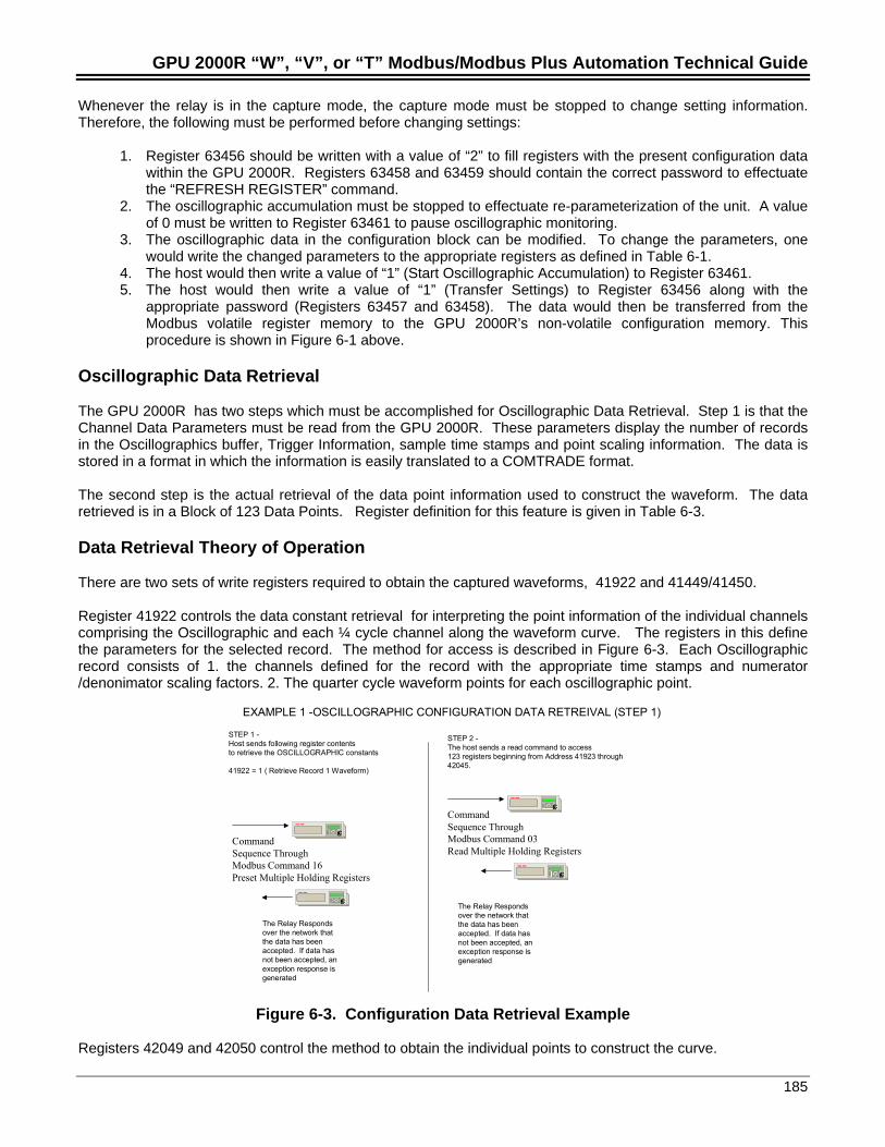
GPU 2000R “W”, “V”, or “T” Modbus/Modbus Plus Automation Technical Guide
185
Whenever the relay is in the capture mode, the capture mode must be stopped to change setting information.Therefore, the following must be performed before changing settings:
1. Register 63456 should be written with a value of “2” to fill registers with the present configuration datawithin the GPU 2000R. Registers 63458 and 63459 should contain the correct password to effectuatethe “REFRESH REGISTER” command.
2. The oscillographic accumulation must be stopped to effectuate re-parameterization of the unit. A valueof 0 must be written to Register 63461 to pause oscillographic monitoring.
3. The oscillographic data in the configuration block can be modified. To change the parameters, onewould write the changed parameters to the appropriate registers as defined in Table 6-1.
4. The host would then write a value of “1” (Start Oscillographic Accumulation) to Register 63461.5. The host would then write a value of “1” (Transfer Settings) to Register 63456 along with the
appropriate password (Registers 63457 and 63458). The data would then be transferred from theModbus volatile register memory to the GPU 2000R’s non-volatile configuration memory. Thisprocedure is shown in Figure 6-1 above.
Oscillographic Data Retrieval
The GPU 2000R has two steps which must be accomplished for Oscillographic Data Retrieval. Step 1 is that theChannel Data Parameters must be read from the GPU 2000R. These parameters display the number of recordsin the Oscillographics buffer, Trigger Information, sample time stamps and point scaling information. The data isstored in a format in which the information is easily translated to a COMTRADE format.
The second step is the actual retrieval of the data point information used to construct the waveform. The dataretrieved is in a Block of 123 Data Points. Register definition for this feature is given in Table 6-3.
Data Retrieval Theory of Operation
There are two sets of write registers required to obtain the captured waveforms, 41922 and 41449/41450.
Register 41922 controls the data constant retrieval for interpreting the point information of the individual channelscomprising the Oscillographic and each ¼ cycle channel along the waveform curve. The registers in this definethe parameters for the selected record. The method for access is described in Figure 6-3. Each Oscillographicrecord consists of 1. the channels defined for the record with the appropriate time stamps and numerator/denonimator scaling factors. 2. The quarter cycle waveform points for each oscillographic point.
ECCommandSequence ThroughModbus Command 16Preset Multiple Holding Registers
STEP 1 -Host sends following register contentsto retrieve the OSCILLOGRAPHIC constants
41922 = 1 ( Retrieve Record 1 Waveform)
EXAMPLE 1 -OSCILLOGRAPHIC CONFIGURATION DATA RETREIVAL (STEP 1)
EC
ECCommandSequence ThroughModbus Command 03Read Multiple Holding Registers
STEP 2 -The host sends a read command to access123 registers beginning from Address 41923 through 42045.
EC
The Relay Respondsover the network that the data has been accepted. If data has not been accepted, anexception response isgenerated
The Relay Respondsover the network that the data has been accepted. If data has not been accepted, anexception response isgenerated
Figure 6-3. Configuration Data Retrieval Example
Registers 42049 and 42050 control the method to obtain the individual points to construct the curve.
GPU 2000R “W”, “V”, or “T” Modbus/Modbus Plus Automation Technical Guide
186
Each waveform consists of 106 points. The GPU2000R stores the waveform and transfers the data to the host inquarter cycle blocks.
The steps required to read the data are as such:
Write the record number and quarter cycle block to access (Register 42049 = 1 for read first Record and42050 to read the 1 st quarter cycle in the Block of Data). The GPU 2000R shall reset the control register to0.
Read the block of point data. Write the Record Number and quarter cycle block to access (Register 42050 = 2 for read next Quarter Cycle
Block of Data). The GPU2000R shall reset the control register to 0. Read the Block of point data. If register 42050 is not equal to 0, repeat the previous two steps.
The process is illustrated pictorially in Figure 6-4.
DPU REGISTER 4X OSCILLOGRAPHICS MAP MEMORY
Data Control Register
OscillographicConfigurationSettings
..
EC
Not ViewableBy Operator
Viewable Via Modbus/Modbus Plus
Record Number Desired 42049
42050
42051
4205242053
42162
RESERVED
Quarter Cycles In Record
1st Quarter Cycle
2nd Quarter Cycle
3rd Quarter Cycle
Nth Quarter Cycle
RECORD N
1st Quarter Cycle
2nd Quarter Cycle
3rd Quarter Cycle
Nth Quarter Cycle
RECORD 1
Write Record Number Required
Write Quarter Cycle Block Desired
Read Quarter Cycle Data
Figure 6-4. Memory Map Philosophy for Oscillographics Waveform Retrieval
Table 6-2. Oscillographic Data Format Retrieval Block
RegisterAddress
Item Description
CHANNEL DATA42049 WRITE DATA – Record Number For
Data DesiredUnsigned Integer (16 Bits)Number Of Record to Be ACCESSED (Seecalculation for the maximum number of recordscapable to be stored.)
42050 WRITE DATA- DATA CONTROL Unsigned Integer (16 Bits)1 = First Quarter Cycle of Data2 = NEXT Quarter Cycle of Data3 = Repeat Quarter Cycle of Data
42051 READ DATA –RESERVED
Unsigned Integer (16 Bits)RESERVED
42052 READ DATA – Number of QuarterCycles Remaining to be read withinthe record accessed
Unsigned Integer (16 Bits)RESERVED
42053 Fault Trigger FlagBit 0 = Reserved (lsb)Bit 1 = 50 IEBit 2 = 27-1PBit 3 = 27-3P
Unsigned Integer 16 BitsReservedInadvertent EnergizationSingle Phase Undervoltage AlarmThree Phase Undervoltage Alarm
GPU 2000R “W”, “V”, or “T” Modbus/Modbus Plus Automation Technical Guide
187
RegisterAddress
Item Description
Bit 4 = 27GBit 5 = 59Bit 6 = 59GBit 7 = 24Bit 8 = 21-1aBit 9 = 21-1Bit 10 = 21-2Bit 11 = 81U1Bit 12 = 81U2Bit 13 = 81O1Bit 14 = 81O2Bit 15 = Reserved
Third Harmonic Stator Ground UndervoltageOvervoltage AlarmGround Overvoltage AlarmVolts Per Hertz AlarmZone 1a Impedance TripZone 1 Impedance TripZone 2 Impedance TripUnderfrequency First Stage TripUnderfrequency Second Stage TripOverfrequency First Stage TripOverfrequency Second Stage TripReserved
42054 Fault Trigger FlagBit 0 = 32 FU (lsb)Bit 1 = 32RBit 2 = 40Bit 3 = 46QBit 4 = 50PBit 5 = 50GBit 6 = 51PBit 7 = 51GBit 8 = 51VCBit 9 = 51VRBit10 = 67PBit 11 = 67NBit 12 = 87MBit 13 = 87GBit 14 = 32FOBit 15 = RESERVED (msb)
Unsigned Integer 16 Bits Start Capture on:Forward Underpower TripReverse Power TripLoss of Excitation AlarmNegative –Sequence Overpower TripPhase Instantaneous Overcurrent TripGround Instantaneous Overcurrent TripPhase Time Overcurrent TripGround Time Overcurrent TripVoltage-controlled Time OC TripVoltage-restrained Time OC TripPhase Directional Time-Overcurrent TripGround Directional Time Overcurrent TripMachine Differential TripDifferential Ground Trip (Restrictive Earth Fault)Forward Overpower TripRESERVED
42055 Pickup Trigger FlagBit 0 = Reserved (lsb)Bit 1 = 50 IEBit 2 = 27-1PBit 3 = 27-3PBit 4 = 27GBit 5 = 59Bit 6 = 59GBit 7 = 24Bit 8 = 21-1aBit 9 = 21-1Bit 10 = 21-2Bit 11= 81U1Bit 12 = 81U2Bit 13 = 81O1Bit 14 = 81O2Bit 15 = Reserved
Unsigned Integer 16 BitsReservedInadvertent EnergizationSingle Phase Undervoltage AlarmThree Phase Undervoltage AlarmThird Harmonic Stator Ground UndervoltageOvervoltage AlarmGround Overvoltage AlarmVolts Per Hertz AlarmZone 1a Impedance TripZone 1 Impedance TripZone 2 Impedance TripUnderfrequency First Stage TripUnderfrequency Second Stage TripOverfrequency First Stage TripOverfrequency Second Stage TripReserved
42056 Pickup Trigger FlagBit 0 = 32 FU (lsb)Bit 1 = 32RBit 2 = 40Bit 3 = 46QBit 4 = 50PBit 5 = 50GBit 6 = 51PBit 7 = 51GBit 8 = 51VC
Unsigned Integer 16 Bits Start Capture on:Forward Underpower TripReverse Power TripLoss of Excitation AlarmNegative –Sequence Overpower TripPhase Instantaneous Overcurrent TripGround Instantaneous Overcurrent TripPhase Time Overcurrent TripGround Time Overcurrent TripVoltage-controlled Time OC Trip
GPU 2000R “W”, “V”, or “T” Modbus/Modbus Plus Automation Technical Guide
188
RegisterAddress
Item Description
Bit 9 = 51VRBit10 = 67PBit 11 = 67NBit 12 = 87MBit 13 = 87GBit 14 = 32FOBit 15 = RESERVED (msb)
Voltage-restrained Time OC TripPhase Directional Time-Overcurrent TripGround Directional Time Overcurrent TripMachine Differential TripDifferential Ground Trip (Restrictive Earth Fault)Forward Overpower TripRESERVED
42057 Miscellaneous Trigger FlagBit 0 = Master Trip (lsb)Bit 1 = 52aBit 2 = Breaker Fail AlarmBit 3 = RESERVEDBit 4 = RESERVEDBit 5 = RESERVEDBit 6 = RESERVEDBit 7 = RESERVEDBit 8 = RESERVEDBit 9 = RESERVEDBit 10 = RESERVEDBit 11 = RESERVEDBit 12 = RESERVEDBit 13 = RESERVEDBit 14 = RESERVEDBit 15 = RESERVED
Unsigned Integer 16 BitsMaster Trip Output Trigger Osc RecordBreaker Change State Triggered Ocs RecordBreaker Fail Alarm Triggered Osc. REcordRESERVEDRESERVEDRESERVEDRESERVEDRESERVEDRESERVEDRESERVEDRESERVEDRESERVEDRESERVEDRESERVEDRESERVEDRESERVED
42058 Pickup Trigger FlagBit 0 = RESERVED (lsb)Bit 1 = RESERVEDBit 2 = RESERVEDBit 3 = RESERVEDBit 4 = RESERVEDBit 5 = RESERVEDBit 6 = RESERVEDBit 7 = RESERVEDBit 8 = RESERVEDBit 9 = RESERVEDBit10 = RESERVEDBit 11 = RESERVEDBit 12 = RESERVEDBit 13 = RESERVEDBit 14 = RESERVEDBit 15 = RESERVED (msb)
Unsigned Integer 16 Bits Start Capture on:RESERVEDRESERVEDRESERVEDRESERVEDRESERVEDRESERVEDRESERVEDRESERVEDRESERVEDRESERVEDRESERVEDRESERVEDRESERVEDRESERVEDRESERVEDRESERVED
42059 Data point as described in the configuration block42060 Data point as described in the configuration block42061 Data point as described in the configuration block42062 Data point as described in the configuration block42063 Data point as described in the configuration block42064 Data point as described in the configuration block42065 Data point as described in the configuration block42066 Data point as described in the configuration block42067 Data point as described in the configuration block42068 Data point as described in the configuration block42069 Data point as described in the configuration block42070 Data point as described in the configuration block42071 Data point as described in the configuration block42072 Data point as described in the configuration block
GPU 2000R “W”, “V”, or “T” Modbus/Modbus Plus Automation Technical Guide
189
RegisterAddress
Item Description
42073 Data point as described in the configuration block42074 Data point as described in the configuration block42075 Data point as described in the configuration block42076 Data point as described in the configuration block42077 Data point as described in the configuration block42078 Data point as described in the configuration block42079 Data point as described in the configuration block42080 Data point as described in the configuration block42081 Data point as described in the configuration block42082 Data point as described in the configuration block42083 Data point as described in the configuration block42084 Data point as described in the configuration block42085 Data point as described in the configuration block42086 Data point as described in the configuration block42087 Data point as described in the configuration block42088 Data point as described in the configuration block42089 Data point as described in the configuration block42090 Data point as described in the configuration block42091 Data point as described in the configuration block42092 Data point as described in the configuration block42093 Data point as described in the configuration block42094 Data point as described in the configuration block42095 Data point as described in the configuration block42096 Data point as described in the configuration block42097 Data point as described in the configuration block42098 Data point as described in the configuration block42099 Data point as described in the configuration block42100 Data point as described in the configuration block42101 Data point as described in the configuration block42102 Data point as described in the configuration block42103 Data point as described in the configuration block42104 Data point as described in the configuration block42105 Data point as described in the configuration block42106 Data point as described in the configuration block42107 Data point as described in the configuration block42108 Data point as described in the configuration block42109 Data point as described in the configuration block42110 Data point as described in the configuration block42111 Data point as described in the configuration block42112 Data point as described in the configuration block42113 Data point as described in the configuration block42114 Data point as described in the configuration block42115 Data point as described in the configuration block42116 Data point as described in the configuration block42117 Data point as described in the configuration block42118 Data point as described in the configuration block42119 Data point as described in the configuration block42120 Data point as described in the configuration block42121 Data point as described in the configuration block42122 Data point as described in the configuration block42123 Data point as described in the configuration block42124 Data point as described in the configuration block42125 Data point as described in the configuration block
GPU 2000R “W”, “V”, or “T” Modbus/Modbus Plus Automation Technical Guide
190
RegisterAddress
Item Description
42126 Data point as described in the configuration block42127 Data point as described in the configuration block42128 Data point as described in the configuration block42129 Data point as described in the configuration block42130 Data point as described in the configuration block42131 Data point as described in the configuration block42132 Data point as described in the configuration block42133 Data point as described in the configuration block42134 Data point as described in the configuration block42135 Data point as described in the configuration block42136 Data point as described in the configuration block42137 Data point as described in the configuration block42138 Data point as described in the configuration block42139 Data point as described in the configuration block42140 Data point as described in the configuration block42141 Data point as described in the configuration block42142 Data point as described in the configuration block42143 Data point as described in the configuration block42144 Data point as described in the configuration block42145 Data point as described in the configuration block42146 Data point as described in the configuration block42147 Data point as described in the configuration block42148 Data point as described in the configuration block42149 Data point as described in the configuration block42150 Data point as described in the configuration block42151 Data point as described in the configuration block42152 Data point as described in the configuration block42153 Data point as described in the configuration block42154 Data point as described in the configuration block42155 Data point as described in the configuration block42156 Data point as described in the configuration block42157 Data point as described in the configuration block42158 Data point as described in the configuration block42159 Data point as described in the configuration block42160 Data point as described in the configuration block42161 Data point as described in the configuration block42162 Data point as described in the configuration block
Oscillographic Data Interpretation
Up to 13 channels may be assigned to a ¼ cycle buffer read. The following diagram interprets the contents of thebuffer if 1, 2, or 4 channels are selected for storage.
For each quarter cycle, the GPU 2000R takes eight samples of data for each channel specified when the newacquisition was setup by the oscillographic control in the 6X registers, specifically Register 63468. Examplesfollow.
IF1 CHANNEL IS SELECTED FOR STORAGE
REGISTER NUMBER SAMPLES
42059 s1ch142060 s2 ch142061 s3 ch1
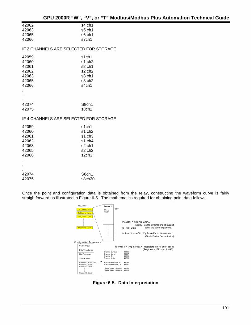
GPU 2000R “W”, “V”, or “T” Modbus/Modbus Plus Automation Technical Guide
191
42062 s4 ch142063 s5 ch142065 s6 ch142066 s7ch1
IF 2 CHANNELS ARE SELECTED FOR STORAGE
42059 s1ch142060 s1 ch242061 s2 ch142062 s2 ch242063 s3 ch142065 s3 ch242066 s4ch1...42074 S8ch142075 s8ch2
IF 4 CHANNELS ARE SELECTED FOR STORAGE
42059 s1ch142060 s1 ch242061 s1 ch342062 s1 ch442063 s2 ch142065 s2 ch242066 s2ch3...42074 S8ch142075 s8ch20
Once the point and configuration data is obtained from the relay, constructing the waveform curve is fairlystraightforward as illustrated in Figure 6-5. The mathematics required for obtaining point data follows:
1st Quarter Cycle
2nd Quarter Cycle
3rd Quarter Cycle
Nth Quarter Cycle
RECORD 1
SeeExampleabove
Sample 142059
EXAMPLE CALCULATION
Ia Point Data
Ia Point 1 = Ia Ch 1 X ( Scale Factor Numerator)(Scale Factor Denominator)
Ia Point 1 = (reg 41803) X ( Registers 41677 and 41685)(Registers 41692 and 41693)
Configuration Parameters
NOTE : Voltage Points are calculatedusing the same equations.
Control/Status
Date/Timestamps
Line Frequency
Sample Rates
Channel 1 ScaleChannel 2 ScaleChannel 3 Scale
Channel 8 Scale
Channel NumberChannel NameChannel IDChannel Units
Num. Scale Factor HiNum. Scale Factor Lo
Denom Scale Factor HiDenom Scale Factor Lo
41686416874168841689
4169041691
4169241693
Figure 6-5. Data Interpretation
GPU 2000R “W”, “V”, or “T” Modbus/Modbus Plus Automation Technical Guide
192
Modbus Conclusion
Modbus ASCII Communication Test Example
The easiest method to initiate communications in the MODBUS protocol is to read known discrete and registerdata. As per the GPU 2000R Modbus register documentation, the unit catalog number is resident at register40133. A list of the register definitions of the GPU 2000R is presented and explained in the next section. A ReadHolding Register Modbus Command is explained. Documentation is available from Groupe Schneider furtherdescribing the Modbus ASCII emulation characteristics. The explanation contained within this document isintended to be a quick start guide to communication initiation.
The length of the catalog number is 12 characters or 6 registers. The following command string format, whensent will retrieve the catalog number from the unit.
: 01 03 00 83 00 06 73 lf cr
The above string in MODBUS ASCII format should be sent:
3A 30 31 30 33 30 30 38 33 30 30 30 36 37 33 0D 0A
The string is translated as such:
Colon (in HEX) , unit address = 01 (in HEX) , Read Holding Registers (Code 3 in HEX), data memory desiredaddress –1 = 132 decimal (0084 in HEX), number of registers read = 6 (0006 in HEX), message calculated LRCcode 72 (37 32), and line feed (0D) and (0A).
A typical response shall include the following:
: Address number (01), Read Holding Registers Command (Code 3 in HEX), Byte Count Returned in decimal (0Cin HEX 12 bytes in decimal) , Data Register 40133 = 3538 hex – 58 ASCII, Data Register 40134= 3743 hex , 7CASCII , Data Register 40135 = 3034, 04 ASCII, Data Register 40136 = 3132 hex, 32 ASCII, Data Register 40137= 3631 HEX, 61 ASCII, Data Register 40138 = 3131HEX, 11 ASCII, and calculated LRC =79 (HEX) and linefeed with carriage return (0D 0A).
The aforementioned response would be returned as such:
3A 30 31 30 33 30 43 35 38 37 43 30 34 31 32 36 31 31 31 37 39 0A 0D.
Calculation of the LRC (Longitudinal Redundancy Code)
Modbus ASCII protocol uses a Longitudinal Redundancy Code to verify correct reception of the command. Thiserror check is used in addition to the parity option (used by the UART in the PC) and other data such as the bytecount which verifies data returned. The process for calculation of the checksum is described as such:
1. Add all bytes in the message except for the colon, line feed, and carriage return. Exclude the LRCchecksum which in included in the message structure.
2. Invert all bits in the word after the addition.3. Add 1 to the inverted result. This is the checksum.
An example is as follows:Command sent:
3A 30 31 30 33 30 30 38 33 30 30 30 36 37 33 0D 0A
GPU 2000R “W”, “V”, or “T” Modbus/Modbus Plus Automation Technical Guide
193
Decode of the data from ASCII to HEX yields.
: 01 03 00 83 00 06 73 lf cr
The decoded LRC checksum is 73. The calculation of the checksum is as such:
1. Neglect the colon (3A) and the lf (Line Feed 0A) and cr (Carriage Return OD). This decreases thestring to
2. The LRC checksum 73 (37 33 in ASCII) should also be saved for comparison to the original datastring. The string for LRC calculation is 01 03 00 83 00 06.
3. The byte data should be added thus 01 + 03 + 00 +83 + 00 + 06 = 8D in HEX. Notice that the byteshave been decoded from ASCII before performing the addition.
4. A Two’s compliment must be performed on the number to determine the LRC Checksum. Inversionof the number 8D hex yields 72 hex.
5. To complete the Two’s compliment addition for accurate compilation of the checksum 1 hex must beadded to the inverted bits to yield 72 + 1 = 73 HEX. Thus the two calculated values agree.
Please reference the Modicon Modbus Documentation for additional command configuration on each data type(0X, 1X,4X and 6X read write capabilities).
Modbus CRC-16 Calculation
The CRC – 16 error check is much more robust than that of the LRC error check. It is however, a more complexalgorithm to compute. It’s computation is started by setting a word of 16 bits to a value of FFFF hex. A byte ofthe message is logically OR’ed with the register word and then shifted in a predictable method. What follows is areprint from the protocol manufacturer’s manual MODICON MODBUS PROTOCOL REFERENCE GUIDE – PI-MBUS-300 Revision J Dated June 1996 published by Modicon Inc. Industrial Automation Systems, One HighStreet, North Andover, MA 01845.
“The Cyclical Redundancy Check (CRC) field is two bytes, containing a 16 –bit binary value. TheCRC value is calculated by the transmitting device which appends the CRC to the message. Thereceiving device, recalculates a CRC during the receipt of the message, and compares thecalculated value to the value it received in the CRC field. If the two values are not equal, an errorresults”
The CRC is started by first preloading a 16 bit register register to all 1’s. Then a process begins ofapplying successive 8 – bit bytes of the message to the current contents of the register. Only theeight bits of data in each character are used for generating the CRC. Start and stop bits and theparity bit do not apply to the CRC.
During the generation of the CRC, each 8-bit character is exclusive Ored with the registercontents. Then the reslult is shifted in the direction of the least significant bit (LSB), with a zerofilled into the most significant bit (MSB) position. The LSB is extracted and examined. If the LSBwas a 1, the register is then exclusive Ored with a preset, fixed value. If the LSB was a0, noexclusive OR takes place.
The process is repeated until eight shifts have been performed. After the last eighth shift, thenext 8-bit character is exclusive OR‘ed with the register’s current value and the process repeatsfor eight more shifts as described above. The final contents of the register,after all the charactersof the message have been applied, is the CRC value.
A procedure for generating a CRC is
1. Load a 16 Bit Register with FFFF hex (all 1’s) Call this the CRC register.
2. Exclusive OR the first 8-bit byte of the message with the two-order byte of the 16 –bit CRCregister, putting the result in the CRC register.
3. Shift the CRC register one bit to the right (Toward the LSB), zero-filling the MSB. Extractand examine the LSB.
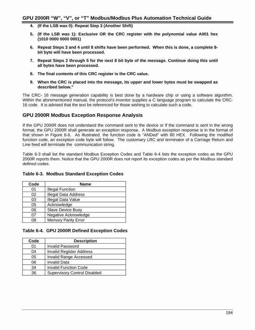
GPU 2000R “W”, “V”, or “T” Modbus/Modbus Plus Automation Technical Guide
194
4. (If the LSB was 0): Repeat Step 3 (Another Shift)
5. (If the LSB was 1): Exclusive OR the CRC register with the polynomial value A001 hex(1010 0000 0000 0001)
6. Repeat Steps 3 and 4 until 8 shifts have been performed. When this is done, a complete 8-bit byte will have been processed.
7. Repeat Steps 2 through 5 for the next 8 bit byte of the message. Continue doing this untilall bytes have been processed.
8. The final contents of this CRC register is the CRC value.
9. When the CRC is placed into the message, its upper and lower bytes must be swapped asdescribed below.”
The CRC- 16 message generation capability is best done by a hardware chip or using a software algorithm.Within the aforementioned manual, the protocol’s inventor supplies a C language program to calculate the CRC-16 code. It is advised that the text be referenced for those wishing to calculate such a code.
GPU 2000R Modbus Exception Response Analysis
If the GPU 2000R does not understand the command sent to the device or if the command is sent in the wrongformat, the GPU 2000R shall generate an exception response. A Modbus exception response is in the format ofthat shown in Figure 6-6. As illustrated, the function code is “ANDed” with 80 HEX. Following the modifiedfunction code, an exception code byte will follow. The customary LRC and terminator of a Carriage Return andLine feed will terminate the communication string.
Table 6-3 shall list the standard Modbus Exception Codes and Table 6-4 lists the exception codes as the GPU2000R reports them. Notice that the GPU 2000R does not report its exception codes as per the Modbus standarddefined codes.
Table 6-3. Modbus Standard Exception Codes
Code Name01 Illegal Function02 Illegal Data Address03 Illegal Data Value05 Acknowledge06 Slave Device Busy07 Negative Acknowledge08 Memory Parity Error
Table 6-4. GPU 2000R Defined Exception Codes
Code Description01 Invalid Password04 Invalid Register Address05 Invalid Range Accessed06 Invalid Data34 Invalid Function Code36 Supervisory Control Disabled
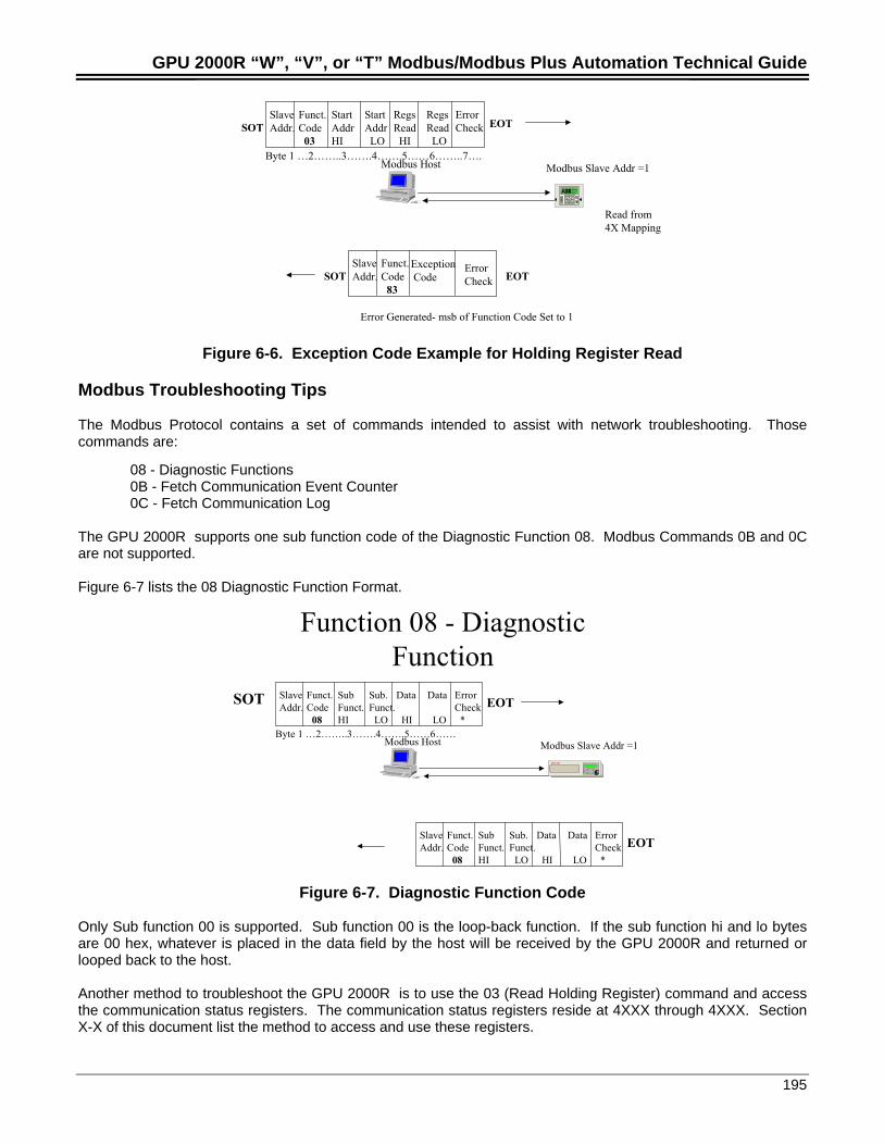
GPU 2000R “W”, “V”, or “T” Modbus/Modbus Plus Automation Technical Guide
195
Modbus Host Modbus Slave Addr =1
Read from 4X Mapping
SlaveAddr.
Funct.Code 03
StartAddrHI
Start Addr LO
RegsRead HI
RegsRead LO
ErrorCheck EOTSOT
Byte 1 …2……..3…….4…….5……6……..7….
SlaveAddr.
Funct.Code 83
Exception Code
ErrorCheck EOTSOT
E
C
NetworkPartnerV1.0
Error Generated- msb of Function Code Set to 1
Figure 6-6. Exception Code Example for Holding Register Read
Modbus Troubleshooting Tips
The Modbus Protocol contains a set of commands intended to assist with network troubleshooting. Thosecommands are:
08 - Diagnostic Functions0B - Fetch Communication Event Counter0C - Fetch Communication Log
The GPU 2000R supports one sub function code of the Diagnostic Function 08. Modbus Commands 0B and 0Care not supported.
Figure 6-7 lists the 08 Diagnostic Function Format.
Function 08 - DiagnosticFunction
Modbus Host
EC
Modbus Slave Addr =1
SlaveAddr.
Funct.Code 08
SubFunct.HI
Sub. Funct. LO
Data
HI
Data
LO
ErrorCheck *
EOT
Byte 1 …2……..3…….4…….5……6……
SOT
SlaveAddr.
Funct.Code 08
SubFunct.HI
Sub. Funct. LO
Data
HI
Data
LO
ErrorCheck *
EOT
Figure 6-7. Diagnostic Function Code
Only Sub function 00 is supported. Sub function 00 is the loop-back function. If the sub function hi and lo bytesare 00 hex, whatever is placed in the data field by the host will be received by the GPU 2000R and returned orlooped back to the host.
Another method to troubleshoot the GPU 2000R is to use the 03 (Read Holding Register) command and accessthe communication status registers. The communication status registers reside at 4XXX through 4XXX. SectionX-X of this document list the method to access and use these registers.
GPU 2000R “W”, “V”, or “T” Modbus/Modbus Plus Automation Technical Guide
196
Finally, it is always advantageous to use a datascope or a communication analyzer when troubleshooting aModbus Network. Such devices allow the implementers to view the data strings between the host and IED.Modicon’s parent company Schneider Electric has designed many utilities and products to assist the networkprofessional with troubleshooting. Such tools are inexpensive when compared to the person-hours spentguessing as to what is sent between a host and IED. Such tools available are at a modest cost, such as Modlink,or at no cost MTS. Many of these tools are available on the website www.modicon.com.
GPU 2000R Modbus ASCII Communication Timing Analysis
Perhaps the most common error in implementing a Modbus ASCII network is timing setup for communication.Modbus ASCII protocol operates according to the following timing rules:
• If the GPU 2000R receives a command without a communication error (LRC, PARITY,FRAMING, OVERRUN … errors), a normal response occurs.
• If the GPU 2000R does not receive a command without a communication error (LRC,PARITY, FRAMING, OVERRUN …. Errors), no response is returned. The host (master)device will sense a timeout according to its timeout parameter. The host could then send anew command or retry sending the original command.
• Modbus ASCII allows for internals up to 1 second between characters are acceptable gaps.The GPU 2000R will not timeout. Character send gaps in excess of 1 second will result inGPU 2000R Modbus port timeouts .
GPU 2000R Modbus network implementers will usually notice communication errors in the form of excessivecommunication retries, errors, or non-responses. Understanding communication timing is a subject rarelycovered in protocol manuals, but an important topic in network implementation.
Network timing is predicated upon the following factors:
Host Latency (How long does it take a host device to generate a command, receive the response andinterpret the data).
Intermediate Device Latency (If a Modem, data concentrator or other device is between the end devicerequired for data retrieval, how long does it take for each device to receive the command and process itdownline to the next device).
GPU 2000R Device Latency (How long does it take for an GPU 2000R to receive a command, and return aresponse to the network).
Baud Rate (How fast is each data bit propagated on the medium. One cannot get around the laws ofphysics)
Protocol Efficiency [Network Bandwidth Utilization] (Does the protocol utilized allow for the issuance ofanother command before a response is received from an outstanding communication request).
The common question to a network system engineer is usually “ How fast can I get my relay alarm data to appearon the screen?”. An analysis of the amount of data and the above 5 areas is required.
Host latency varies widely by manufacturer or the PC or host computer. Software speed and port access varieswidely. Most manufacturers of these hardware and software platforms have general benchmarks to supply to theusers for processing time once the device acquires the data from the communication port.
Intermediate Device Latency also varies from the type of device used. Some modems have a device turnaroundof 5 mS per transactions whereas, a radio modem may require hundreds of mS to obtain an open frequency fromwhich to transmit.
This section shall illustrate and explain a simple network transaction based upon a simple point to pointcommunication from a single GPU 2000R to a host device as illustrated in Figure 6-8 of this document. Thisexample shall exclude SCADA Master host latency.
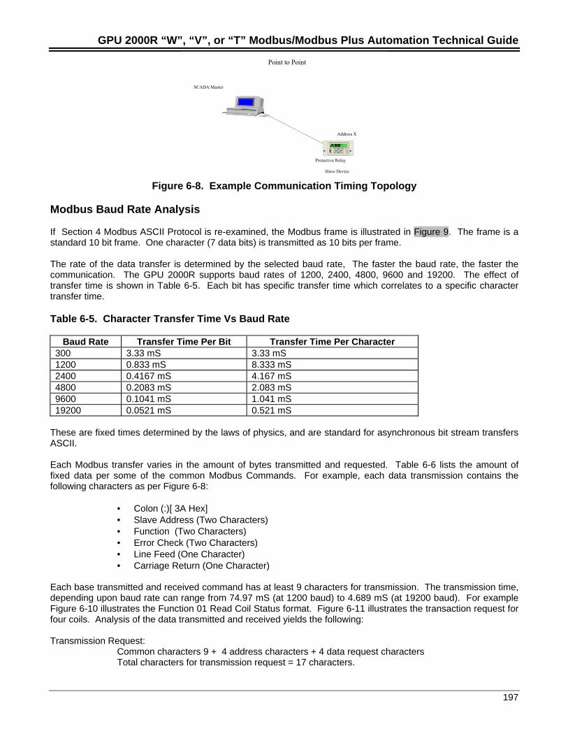
GPU 2000R “W”, “V”, or “T” Modbus/Modbus Plus Automation Technical Guide
197
SCADA Master
Protective Relay
Point to Point
Slave Device
Address X
E
C
NetworkPa rtnerV1 .0
Figure 6-8. Example Communication Timing Topology
Modbus Baud Rate Analysis
If Section 4 Modbus ASCII Protocol is re-examined, the Modbus frame is illustrated in Figure 9. The frame is astandard 10 bit frame. One character (7 data bits) is transmitted as 10 bits per frame.
The rate of the data transfer is determined by the selected baud rate, The faster the baud rate, the faster thecommunication. The GPU 2000R supports baud rates of 1200, 2400, 4800, 9600 and 19200. The effect oftransfer time is shown in Table 6-5. Each bit has specific transfer time which correlates to a specific charactertransfer time.
Table 6-5. Character Transfer Time Vs Baud Rate
Baud Rate Transfer Time Per Bit Transfer Time Per Character300 3.33 mS 3.33 mS1200 0.833 mS 8.333 mS2400 0.4167 mS 4.167 mS4800 0.2083 mS 2.083 mS9600 0.1041 mS 1.041 mS19200 0.0521 mS 0.521 mS
These are fixed times determined by the laws of physics, and are standard for asynchronous bit stream transfersASCII.
Each Modbus transfer varies in the amount of bytes transmitted and requested. Table 6-6 lists the amount offixed data per some of the common Modbus Commands. For example, each data transmission contains thefollowing characters as per Figure 6-8:
• Colon (:)[ 3A Hex]• Slave Address (Two Characters)• Function (Two Characters)• Error Check (Two Characters)• Line Feed (One Character)• Carriage Return (One Character)
Each base transmitted and received command has at least 9 characters for transmission. The transmission time,depending upon baud rate can range from 74.97 mS (at 1200 baud) to 4.689 mS (at 19200 baud). For exampleFigure 6-10 illustrates the Function 01 Read Coil Status format. Figure 6-11 illustrates the transaction request forfour coils. Analysis of the data transmitted and received yields the following:
Transmission Request:Common characters 9 + 4 address characters + 4 data request charactersTotal characters for transmission request = 17 characters.
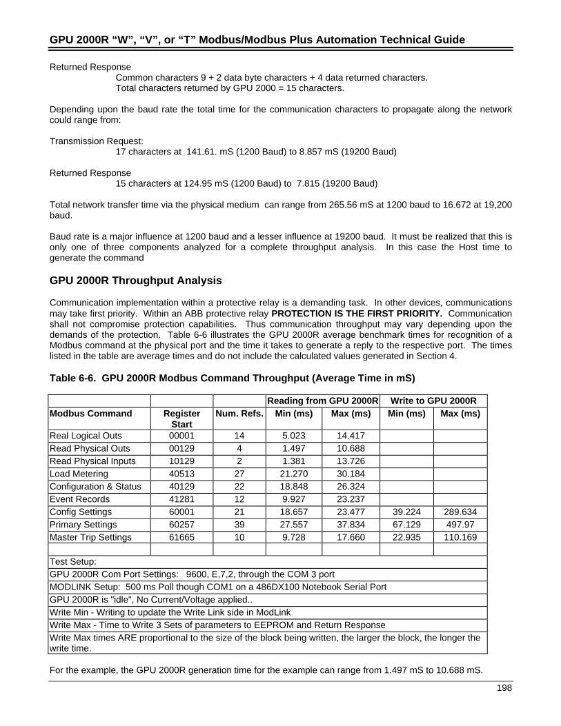
GPU 2000R “W”, “V”, or “T” Modbus/Modbus Plus Automation Technical Guide
198
Returned ResponseCommon characters 9 + 2 data byte characters + 4 data returned characters.Total characters returned by GPU 2000 = 15 characters.
Depending upon the baud rate the total time for the communication characters to propagate along the networkcould range from:
Transmission Request:17 characters at 141.61. mS (1200 Baud) to 8.857 mS (19200 Baud)
Returned Response15 characters at 124.95 mS (1200 Baud) to 7.815 (19200 Baud)
Total network transfer time via the physical medium can range from 265.56 mS at 1200 baud to 16.672 at 19,200baud.
Baud rate is a major influence at 1200 baud and a lesser influence at 19200 baud. It must be realized that this isonly one of three components analyzed for a complete throughput analysis. In this case the Host time togenerate the command
GPU 2000R Throughput Analysis
Communication implementation within a protective relay is a demanding task. In other devices, communicationsmay take first priority. Within an ABB protective relay PROTECTION IS THE FIRST PRIORITY. Communicationshall not compromise protection capabilities. Thus communication throughput may vary depending upon thedemands of the protection. Table 6-6 illustrates the GPU 2000R average benchmark times for recognition of aModbus command at the physical port and the time it takes to generate a reply to the respective port. The timeslisted in the table are average times and do not include the calculated values generated in Section 4.
Table 6-6. GPU 2000R Modbus Command Throughput (Average Time in mS)
Reading from GPU 2000R Write to GPU 2000RModbus Command Register
StartNum. Refs. Min (ms) Max (ms) Min (ms) Max (ms)
Real Logical Outs 00001 14 5.023 14.417Read Physical Outs 00129 4 1.497 10.688Read Physical Inputs 10129 2 1.381 13.726Load Metering 40513 27 21.270 30.184Configuration & Status 40129 22 18.848 26.324Event Records 41281 12 9.927 23.237Config Settings 60001 21 18.657 23.477 39.224 289.634Primary Settings 60257 39 27.557 37.834 67.129 497.97Master Trip Settings 61665 10 9.728 17.660 22.935 110.169
Test Setup:GPU 2000R Com Port Settings: 9600, E,7,2, through the COM 3 portMODLINK Setup: 500 ms Poll though COM1 on a 486DX100 Notebook Serial PortGPU 2000R is "idle", No Current/Voltage applied..Write Min - Writing to update the Write Link side in ModLinkWrite Max - Time to Write 3 Sets of parameters to EEPROM and Return ResponseWrite Max times ARE proportional to the size of the block being written, the larger the block, the longer thewrite time.
For the example, the GPU 2000R generation time for the example can range from 1.497 mS to 10.688 mS.
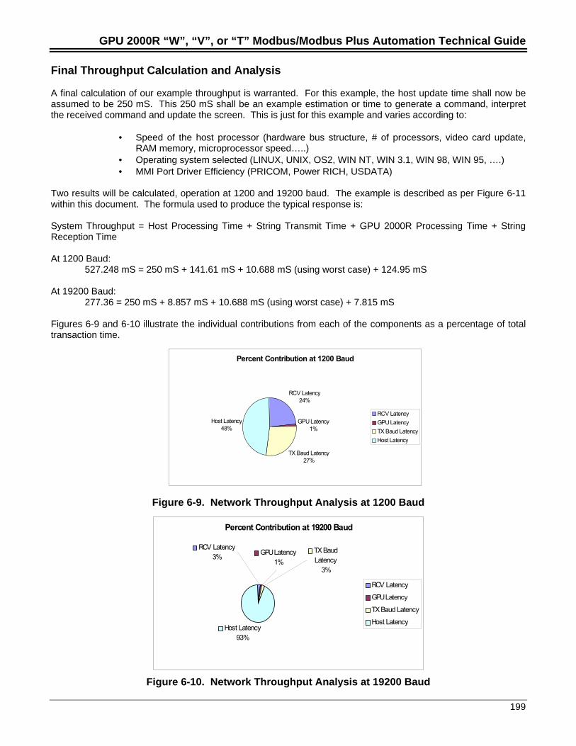
GPU 2000R “W”, “V”, or “T” Modbus/Modbus Plus Automation Technical Guide
199
Final Throughput Calculation and Analysis
A final calculation of our example throughput is warranted. For this example, the host update time shall now beassumed to be 250 mS. This 250 mS shall be an example estimation or time to generate a command, interpretthe received command and update the screen. This is just for this example and varies according to:
• Speed of the host processor (hardware bus structure, # of processors, video card update,RAM memory, microprocessor speed…..)
• Operating system selected (LINUX, UNIX, OS2, WIN NT, WIN 3.1, WIN 98, WIN 95, ….)• MMI Port Driver Efficiency (PRICOM, Power RICH, USDATA)
Two results will be calculated, operation at 1200 and 19200 baud. The example is described as per Figure 6-11within this document. The formula used to produce the typical response is:
System Throughput = Host Processing Time + String Transmit Time + GPU 2000R Processing Time + StringReception Time
At 1200 Baud:527.248 mS = 250 mS + 141.61 mS + 10.688 mS (using worst case) + 124.95 mS
At 19200 Baud:277.36 = 250 mS + 8.857 mS + 10.688 mS (using worst case) + 7.815 mS
Figures 6-9 and 6-10 illustrate the individual contributions from each of the components as a percentage of totaltransaction time.
Percent Contribution at 1200 Baud
RCV Latency24%
GPU Latency1%
TX Baud Latency27%
Host Latency48%
RCV LatencyGPU LatencyTX Baud LatencyHost Latency
Figure 6-9. Network Throughput Analysis at 1200 Baud
Percent Contribution at 19200 Baud
Host Latency93%
GPU Latency1%
RCV Latency3%
TX Baud Latency
3%
RCV Latency
GPU Latency
TX Baud Latency
Host Latency
Figure 6-10. Network Throughput Analysis at 19200 Baud
GPU 2000R “W”, “V”, or “T” Modbus/Modbus Plus Automation Technical Guide
200
Analysis of the simple example yields a few points to be considered when analyzing system throughput. Eachelement involved in communication timing contributes significantly to overall throughput. If the host executed andupdated faster, overall throughput could be improved. If intermediate devices were inserted within the network,transaction time would increase proportionately. Baud rate is only one of many contributing factors in calculatingsystem throughput. If one network access was required for retrieval of system data, overall network efficiencywould be improved. If in a networked system, the protocol utilized would allow for additional data requestcommands while the slave device is processing a response, Network throughput time would be improved.
Virtual treatises have been written on improving system throughput and data updates. This simple exampleillustrates and allows the user to calculate system throughput times. This is especially critical so that the systemuser will not be surprised with overall system response.
ABB has implemented features within the protective relay to maintain system data integrity. Latched bit status,momentary change detect are a few features implemented within the various implementations of the Modbusprotocol.
Modbus Plus Troubleshooting
Schneider Electric has designed Modbus Plus to be a very robust communication network. The publication 890USE 100 00 Version 2.0 titled Modicon Modbus Plus Network Planning and Installation Guide Copyright 1995,AEG Schneider Automation, Inc. details the method for troubleshooting a Modbus Plus network.
There is no communication analyzer for Modbus Plus to view the communication commands occurring over thenetwork. The SA 85 or PCMCIA Modbus Plus adapters have a software utility called MBP STAT which allows apersonal computer to attach to the network allowing a network professional to troubleshoot a Modbus Plusanomaly. Please reference the MBP STAT documentation for use of this valuable troubleshooting tool.
Issues common to Modbus Plus communication errors arise from the following
1. Improper Device Termination. The manufacturer’s in-line and termination connectors must be used.Termination connectors must be used at the end of the lines for a string. The end of the string could be arepeater, bridge, repeater, or end device node.
2. Improper cable used. The manufacturer’s cable should be used in that it is the correct impedance,capacitance and physical wire dimensions to physically mate with the connector.
3. Improper addressing is assumed. The GPU 2000R’s address is in HEX. The Modbus Plus host andMBP STAT uses decimal addressing. Additionally, it must be remembered that an additional byte mustbe appended to the end of the address signifying the path the host wishes to communicate.
4. Improper routing of the cable. The cable should be routed clear of high current devices and wires.Although, Modbus Plus is an industrial network, it is not recommended to route or wrap the cable arounddevices (such as bus bar) which emit EMI/RFI or high current spike devices. The network is a serialnetwork, branches, or splits are not allowed in the cabling. If such configurations are necessary, pleaseuse fiber optics.
5. Improper grounding of the cable.
If proper care is not taken in the planning and installation of the network, the time saved on planning andinstallation is usually spent and exceeded in troubleshooting of the network. Since Modbus Plus is a serialnetwork, any loose connection, impedance mismatch, or anomaly is usually difficult to find. Cable planning andinstallation errors are usually seen as communication errors or retries seen using the MBP STAT utility. Thecable must be checked for continuity (in case of damage) and usually the cable must be disconnected and thecable sections checked.
A copy of the device troubleshooting section from the aforementioned Modbus Plus text is included for the benefitof the reader. The section covers cable continuity.

GPU 2000R “W”, “V”, or “T” Modbus/Modbus Plus Automation Technical Guide
201
Before checking continuity, disconnect all network cable connectors from the node devices-leave the dropcable ground lugs (ed. Note – if any since the tap and drop connectors have ground lugs whereas thedark and light grey connectors do not) to their site panel grounds.
At any node device connector, measure the resistance between pins 2 and 3 (the signal pins), in therange of 60..80 Ω, which include the cable wire resistance.
At each node device connector, check for an open circuit between pin 2 (a signal pin) and pin 1 (theshield pin); then check between pin 3 (a signal pin) and pin 1 – an open circuit should exist for bothchecks.
At each connector, check the continuity between pin 1 and the plant ground point on the local site panelor frame – direct continuity should be present.
If the above continuity checks are not consistent, break the network at various points, and it is recommended thata termination connector be selected at the break. Perform the above tests using MBP STAT and the continuitytests outlined above until the error rate is at a negligible level.
Also as with the Modbus test procedures, Modbus Plus has access to the communication status registers.Another method to troubleshoot the GPU 2000R is to use Read 4X Holding Register command via a DDE editoror a PLC’s MSTR instruction. The communication status registers may then be accessed. The communicationstatus registers reside at 40712 through 40179. Section X-X of this document lists the method to access and usethese registers.
Modbus Plus Throughput
The Manual Titled Modicon Modbus Plus Network Planning and Installation Guide Copyright 1995, AEGSchneider Automation, Inc., lists the methods to calculate Modbus Plus network throughput. It is recommendedthat the aforementioned text be consulted to perform a specific network throughput analysis.
The same principles for any protocol analysis apply to Modbus Plus Protocol analysis. Modbus Plus is a veryefficient protocol since it’s bandwidth is effectively utilized by using the hybrid features of an HDLC protocol withtoken passing. The ability of the network to carry out 32 individual conversations and 2 Global Data broadcastconversations is a very useful capability of the network. Combined with a high baud rate of over 1 megabaud, fastthroughput is assured.
A typical Modbus Plus network is depicted in Figure X-X. A Programmable Logic Controller is connected to aGPU 2000R protective relay accessing data along one of its 8 data slave paths. A Personal Computer Host is notused as a device in this example since it is difficult to predict the latency of the host device. As seen from theexample calculated with Modbus, host latency (in this case the PLC), network latency, and IED latency (GPU2000R) all must be evaluated in their contributions to overall network throughput. The PLC is using a Masterinstruction to access data on the network. The amount of logic in the PLC is 1K of ladder instructions operatingwith a combined scan rate of 4 mS per K of logic. A PLC physical input is assumed to be using in triggering thedata for this example. The latency of the I/O module is assumed to be 1 mS (125 VDC Input Module)
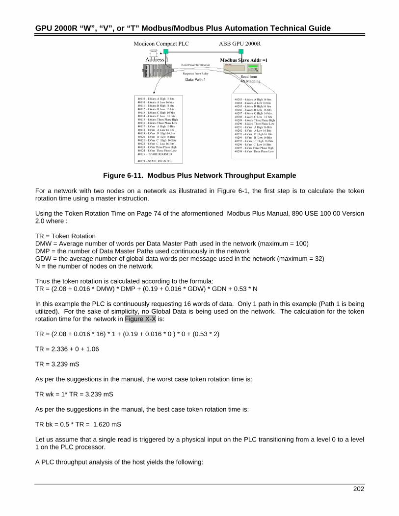
GPU 2000R “W”, “V”, or “T” Modbus/Modbus Plus Automation Technical Guide
202
Address 1
EC
Modbus Slave Addr =1
Read from 4X Mapping
40283 - kWatts A High 16 bits40284 - kWatts A Low 16 bits40285 - kWatts B High 16 bits40286 - kWatts B Low 16 bits40287 - kWatts C High 16 bits40288 - kWatts C Low 16 bits40289 - kWatts Three Phase High40290 - kWatts Three Phase Low40291 - kVars A High 16 Bits40292 - kVars A Low 16 Bits40293 - kVars B High 16 Bits40294 - kVars B Low 16 Bits40295 - kVars C High 16 Bits40296 - kVars C Low 16 Bits40297 - kVars Three Phase High40298 - kVars Three Phase Low
Read Power Information
Response From Relay
40110 - kWatts A High 16 bits40110 - kWatts A Low 16 bits40111 - kWatts B High 16 bits40112 - kWatts B Low 16 bits40113 - kWatts C High 16 bits40114 - kWatts C Low 16 bits40115 - kWatts Three Phase High40116 - kWatts Three Phase Low40117 - kVars A High 16 Bits40118 - kVars A Low 16 Bits40119 - kVars B High 16 Bits40120 - kVars B Low 16 Bits40121 - kVars C High 16 Bits40122 - kVars C Low 16 Bits40123 - kVars Three Phase High40124 - kVars Three Phase Low40125 - SPARE REGISTER :40139 - SPARE REGISTER
Modicon Compact PLC ABB GPU 2000RMSTR
Data Path 1
Figure 6-11. Modbus Plus Network Throughput Example
For a network with two nodes on a network as illustrated in Figure 6-1, the first step is to calculate the tokenrotation time using a master instruction.
Using the Token Rotation Time on Page 74 of the aformentioned Modbus Plus Manual, 890 USE 100 00 Version2.0 where :
TR = Token RotationDMW = Average number of words per Data Master Path used in the network (maximum = 100)DMP = the number of Data Master Paths used continuously in the networkGDW = the average number of global data words per message used in the network (maximum = 32)N = the number of nodes on the network.
Thus the token rotation is calculated according to the formula:TR = (2.08 + 0.016 * DMW) * DMP + (0.19 + 0.016 * GDW) * GDN + 0.53 * N
In this example the PLC is continuously requesting 16 words of data. Only 1 path in this example (Path 1 is beingutilized). For the sake of simplicity, no Global Data is being used on the network. The calculation for the tokenrotation time for the network in Figure X-X is:
TR = (2.08 + 0.016 * 16) * 1 + (0.19 + 0.016 * 0 ) * 0 + (0.53 * 2)
TR = 2.336 + 0 + 1.06
TR = 3.239 mS
As per the suggestions in the manual, the worst case token rotation time is:
TR wk = 1* TR = 3.239 mS
As per the suggestions in the manual, the best case token rotation time is:
TR bk = 0.5 * TR = 1.620 mS
Let us assume that a single read is triggered by a physical input on the PLC transitioning from a level 0 to a level1 on the PLC processor.
A PLC throughput analysis of the host yields the following:

GPU 2000R “W”, “V”, or “T” Modbus/Modbus Plus Automation Technical Guide
203
PLC Input Delay = 1mSPLC Scan = 4 mS per K : 2 scans of the PLC = 8 mS = 2 * 4 mS
PLC Scan and Delay = 5 mS best case and 9 mS worst Case
It is interesting to note that 32 words of Global Data (if used in this calculation) were requested. An additionaltoken rotation time of (32* 0.016) * 1 = 0.512 mS would be added to a token rotation worst case (0.256 averagecontribution to the network otherwise). Thus with Global data, the average contribution for a single transactionwould be 1.024 mS worst case for each network transaction.