fyp final report-libre
TRANSCRIPT
7/21/2019 FYP Final Report-libre
http://slidepdf.com/reader/full/fyp-final-report-libre 1/109
HARDWARE IMPLEMENTATION OF OFDM TRASNMITTER ANDRECEIVER USING FPGA
SHAHBAZ ABBASI s051.04SHAZER BAIG s303.04
INTERNAL ADVISORDR. IMRAN TASADDUQ
EXTERNAL ADVISORENGR. MUSTAFA IMRAN
NATIONAL UNIVERSITY OF COMPUTER AND EMERGING SCIENCES - FAST JUNE 2008
7/21/2019 FYP Final Report-libre
http://slidepdf.com/reader/full/fyp-final-report-libre 2/109
HARDWARE IMPLEMENTATION OF OFDM TRANSMITTER AND RECEIVERUSING FPGA
BY
SHAHBAZ ABBASI s051.04SHAZER BAIG s303.04
Report submitted in partial fulfilment of the requirementsfor the degree
of Bachelor of Sciencein Telecommunication /Computer Engineering
DEPARTMENT OF TELECOM AND COMPUTER ENGINEERING
NATIONAL UNIVERSITY OF COMPUTER AND EMERGING SCIENCES - FAST
JUNE 2008

7/21/2019 FYP Final Report-libre
http://slidepdf.com/reader/full/fyp-final-report-libre 3/109
ii
ACKNOWLEDGEMENT
First of all we would like to thank Almighty Allah. Its only because of the blessings of Allah
that we have been able to complete our project successfully.
We take this special occasion to thank our parents. We dedicated this work to our parents.
We really have to express our collective gratitude towards our internal advisor Dr. Imran
Tasadduq for all his help, invaluable guidance, critics and generous support throughout our
final year project. We really appreciate the way he mentored us throughout our brief
encounters with the world of Digital Communications.
We also like to thank our external advisor Mr. Mustafa Imran for his enlightening
suggestions and advices. His professionalism, guidance, thoroughness, dedication and
inspirations will always serve to us as an example in our professional life.
Special acknowledgements to Ms. Samreen Amir and Mr. Wasif Shams. Their interest in
this project was very beneficial and helped design many vital parts of the project.
Finally, we would like to thank DIGITEK Engineering for providing us with ModelSim 6.1e
and the ip cores of Viterbi decoder and Reed Solomon decoder that made the difficult task
of implementation of the OFDM receiver much easier.
Shahbaz Abbasi s051.04Shazer Baig s303.04
June 2008
7/21/2019 FYP Final Report-libre
http://slidepdf.com/reader/full/fyp-final-report-libre 4/109
iii
TABLE OF CONTENTS
Page
ACKNOWLEDGEMENT ii
TABLE OF CONTENTS iii
LIST OF TABLES vi
LIST OF FIGURES vii
ABSTRACT ix
CHAPTER 1: INTRODUCTION 1
1.1 Introduction 11.2 Digital communication system architecture 1
1.3 Orthogonal Frequency Division Multiplexing 2
1.4 A Typical OFDM system 3
1.4.1 Scrambler / Descrambler 4
1.4.2 Reed Solomon Encoder / Decoder 5
1.4.3 Convolutional Encoder / Decoder 5
1.4.4 Interleaver / De-interleaver 6
1.4.5 Constellation Mapper / De-mapper 61.4.6 FFT / IFFT 6
1.4.7 Cyclic Prefix Adder / Remover 7
1.5 Field Programmable Gate Array 7
1.6 Project Objective 8
1.7 Project Specifications 8
1.7.1 Transmitter Specifications 10
1.7.2 Receiver Specifications 11
1.8 Project design flow 11
1.9 Project scope 12
CHAPTER 2: LITERATURE SURVEY 13
2.1 Evolution of OFDM 13

7/21/2019 FYP Final Report-libre
http://slidepdf.com/reader/full/fyp-final-report-libre 5/109
iv
2.1.1 History of OFDM 13
2.2 The OFDM system 15
2.3 Advantages and disadvantages of OFDM 16
2.4 Applications of OFDM 17
2.5 Verilog Hardware description Language 17
2.6 Synthesis process in Verilog HDL 18
CHAPTER 3: TRANSMITTER DESIGN AND IMPLEMENTATION 20
3.1 Introduction 20
3.2 OFDM system hardware architecture 20
3.3 The Transmitter 22
3.4 FIFO 24
3.5 Scrambler 24
3.5.1 Design of Scrambler 25
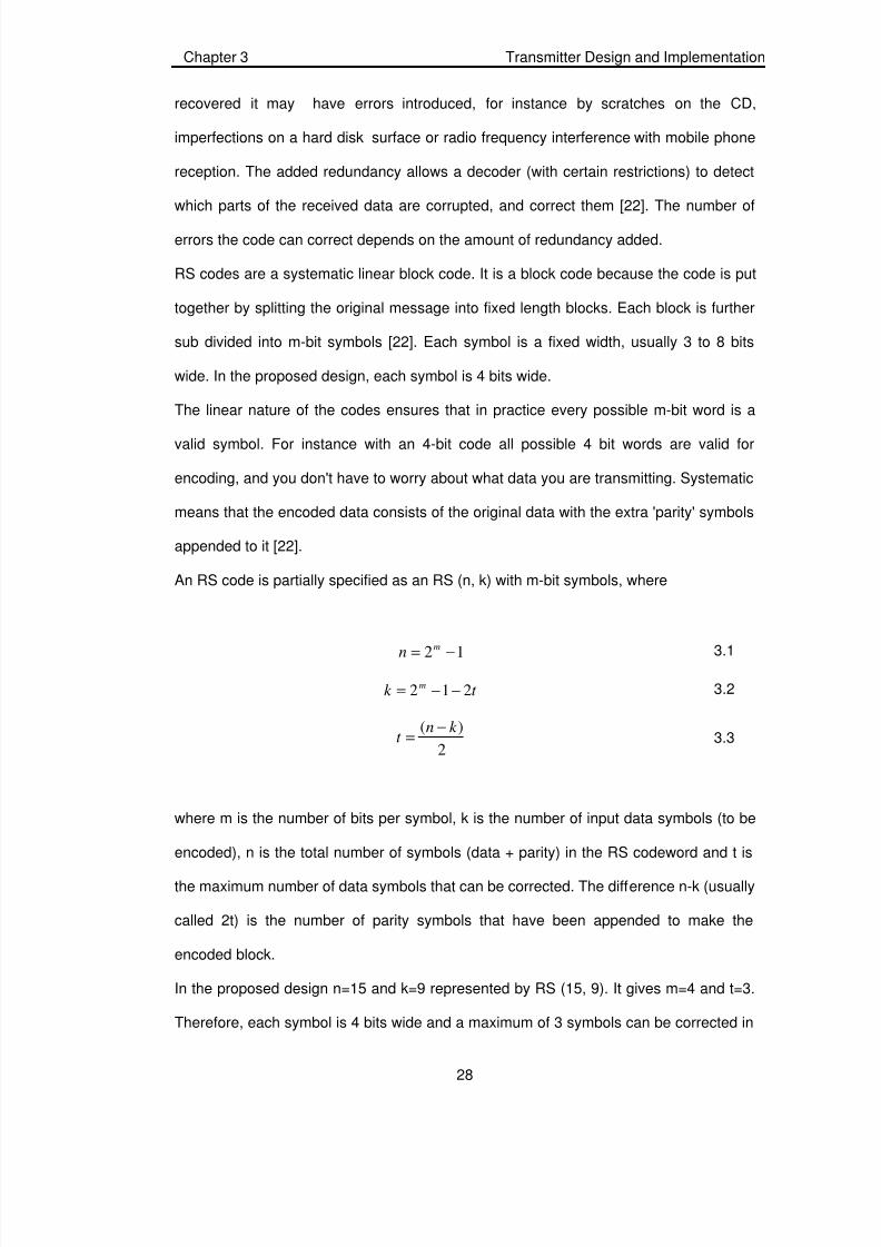
3.6 Reed Solomon Encoder 27
3.6.1 Description of the Reed Solomon code 27
3.6.2 Galois field arithmetic 29
3.6.3 Encoder design 32
3.7 Convolutional Encoder 35
3.7.1 Encoder design 36
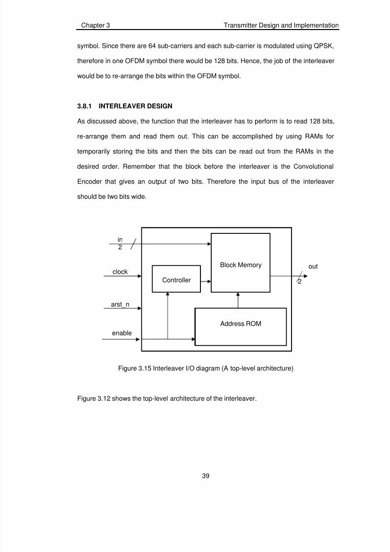
3.8 Interleaver 38
3.8.1 Interleaver design 39
3.9 Constellation mapper 44
3.9.1 Design of Constellation mapper 44
3.10 Inverse Fast Fourier Transform 46
3.10.1 Radix-22 algorithm 47
3.10.2 IFFT design 49
3.11 Cyclic Prefix Adder 523.11.1 Design of Cyclic Prefix Adder 52
CHAPTER 4: RECEIVER DESIGN AND IMPLEMENTATION 54
4.1 Introduction 54
4.2 The Receiver 54

7/21/2019 FYP Final Report-libre
http://slidepdf.com/reader/full/fyp-final-report-libre 6/109
v
4.3 Cyclic Prefix Remover 56
4.4 Fast Fourier Transform 57
4.5 Constellation De-mapper 57
4.5.1 Design of Constellation De-mapper 58
4.6 De-interleaver 59
4.7 Viterbi Decoder 61
4.8 Reed Solomon Decoder 61
4.9 De-scrambler 62
4.9.1 De-scrambler design 62
CHAPTER 5: SIMULATION, SYNTHESIS AND RESULTS 64
5.1 Introduction 64
5.2 Simulation of OFDM Transmitter 64
5.2.1 Scrambler 64
5.2.2 Reed Solomon Encoder 65
5.2.3 Convolutional Encoder 65
5.2.4 Interleaver 66
5.2.5 Constellation mapper 66
5.2.6 IFFT 66
5.2.7 Cyclic Prefix Adder 67
5.3 Synthesis of OFDM Transmitter 68
5.4 Simulation of OFDM Receiver 68
5.4.1 Constellation De-Mapper 68
5.4.2 De-Interleaver 69
5.4.3 De-Scrambler 69
5.5 Synthesis of OFDM Receiver 69
REFERENCES 71
APPENDIX A: RTL CODE IN VERILOG FOR OFDM TRANSMITTER 73
APPENDIX B: RTL CODE IN VERILOG FOR OFDM RECEIVER 97

7/21/2019 FYP Final Report-libre
http://slidepdf.com/reader/full/fyp-final-report-libre 7/109
vi
LIST OF TABLES
Page
2.1 A Brief History of OFDM 13
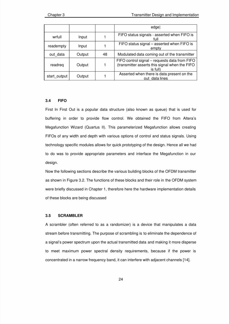
3.1 OFDM system signal descriptions 223.2 Transmitter signal descriptions 23
3.3 Scrambler signal descriptions 25
3.4 Elements of GF (24) and their binary equivalents 30
3.5 Signal descriptions for Reed Solomon Encoder 32
3.6 Signal descriptions for Convolutional Encoder 37
3.7 Signal descriptions for Interleaver 40
3.8 Contents of Address ROM (in Interleaver) 42
3.9 Mapping of bits to constellation points 443.10 Contents of the ROM (in Constellation Mapper) 45
3.11 Signal descriptions for Constellation Mapper 45
3.12 Signal descriptions for IFFT 50
3.13 Signal descriptions for Constellation Mapper 53
4.1 OFDM Receiver signal descriptions 55
4.2 Data points mapped to constellation points 58
4.3 Signal descriptions for Constellation De-mapper 59
4.4 Contents of Address ROM (in De-Interleaver) 604.5 De-scrambler signal descriptions 62
5.1 Important Synthesis results for OFDM Transmitter 68
5.2 Important Synthesis results for OFDM Receiver 69

7/21/2019 FYP Final Report-libre
http://slidepdf.com/reader/full/fyp-final-report-libre 8/109
vii
LIST OF FIGURES
Page
1.1 A typical digital communication system 1
1.2 Spectrum overlap in OFDM 31.3 Complete OFDM system 4
1.4 FPGA design flow 8
1.5 Top level architecture of the proposed OFDM system 9
1.6 OFDM transmitter’s top-level architecture 10
1.7 OFDM receiver’s top-level architecture 11
1.8 Project design flow 12
2.1 Synthesis Process in Verilog Environment 18
3.1 Serial communication format (8 bit data + start bit + stop bit) 203.2 Complete Architecture of the proposed OFDM system
(transmitter highlighted)
21
3.3 I/O view of the OFDM system 22
3.4 I/O diagram of the transmitter 23
3.5 Scrambler I/O diagram 25
3.6 Scrambler logic diagram 26
3.7 Circuit diagram of Scrambler 27
3.8 RS (n, k) code 293.9 Top-level structure of the Reed Solomon Encoder 33
3.10 Detailed architecture of Reed Solomon Encoder 34
3.11 Galois Field multiplier and adder 35
3.12 Convolutional Encoder I/O Diagram 36
3.13 Convolutional Encoder: Circuit Diagram 37
3.14 Interleaving concept 38
3.15 Interleaver I/O diagram (A top-level architecture) 39
3.16 Circuit diagram of Interleaver 42
3.17 QPSK constellation diagram 44
3.18 Constellation Mapper 45
3.19 Radix-4 FFT butterfly 48
3.20 Radix-2 FFT Butterfly 48
3.21 IFFT I/O diagram 50
7/21/2019 FYP Final Report-libre
http://slidepdf.com/reader/full/fyp-final-report-libre 9/109
viii
3.22 Architecture of 64-point-22 FFT 53
3.23 bf2i and bf2ii radix 2 butterflies 51
3.24 Top level architecture of cyclic prefix adder 53
4.1 I/O diagram of the OFDM receiver 54
4.2 Complete Architecture of the proposed OFDM system (receiver
highlighted)
56
4.3 FFT 59
4.4 QPSK constellation diagram 60
4.5 I/O diagram of constellation demapper 60
4.6 Verilog code showing the logic behind implementation of
constellation demapper
61
4.7 De-scrambler I/O diagram 64
4.8 De-scrambler logic diagram 65
5.1 Scrambler simulation results 66
5.2 Solomon Encoder simulation results 67
5.3 Simulation Waveform of the Convolutional Encoder 68
5.4 Constellation Mapper simulation results 68
5.5 IFFT simulation results 69
5.6 Cyclic Prefix Adder simulation result 69

7/21/2019 FYP Final Report-libre
http://slidepdf.com/reader/full/fyp-final-report-libre 10/109
ix
HARDWARE IMPLEMENTATION OF OFDM TRANSMITTER AND RECEIVERUSING FPGA
ABSTRACT
Orthogonal Frequency Division Multiplexing (OFDM) is a multi carrier modulation technique.
It provides high bandwidth efficiency because the carriers are orthogonal to each other and
multiple carriers share the data among themselves. The main advantage of this
transmission technique is its robustness to channel fading in wireless communication
environment. The main objective of this project is to design and implement a baseband
OFDM transmitter and receiver. The implementation has been carried out in hardware using
Field Programmable Gate Array (FPGA). Both the transmitter and the receiver are
implemented on a single FPGA board with the channel being a wired one. The FPGA board
used is Altera’s Cyclone III starter board which contains 24,600 logic elements. The
designing has been done in Verilog HDL. Modelsim 6.1e has been used to simulate the
design. Input to the system is given using computer’s serial port. NI Labview has been used
to do the serial port interfacing. The output of the transmitter has been compared with the
output of MATLAB for the same OFDM system modeled in MATLAB. The data obtained at
the output of the transmitter is fed to the PC using serial port and is converted to complex
numbers because MATLAB gives output in the form of complex numbers. Although error
correction schemes have been employed in the transmitter and the receiver but as the
channel is a wired one, and hence there is no ISI or other channel impairments, therefore
errors don’t occur. Therefore, only the proper operation of the OFDM system has been
aimed to achieve.
7/21/2019 FYP Final Report-libre
http://slidepdf.com/reader/full/fyp-final-report-libre 11/109
Chapter 1 Introduction
1
CHAPTER 1
INTRODUCTION
1.1 INTRODUCTION
Demand for broadband access is increasing at a quick rate, and at the same time, is not
limited to areas that already have an existing high quality infrastructure. For instance,
developing countries and rural areas may not have the existing telecom infrastructure or
the existing connections, typically over copper, to meet the requirements of Digital
Subscriber Line (DSL) technology. Furthermore, it is expected that users will require
more bandwidth on the move. While current technologies can meet this bandwidth
demand, the useful range is limited. This limitation opens up opportunities for
technologies such as Orthogonal Frequency Division Multiplexing.
1.2 DIGITAL COMMUNICATION SYSTEM ARCHITECTURE
OFDM is a digital modulation technique; therefore an introduction to digital
communication systems is being provided. A digital communication system involves the
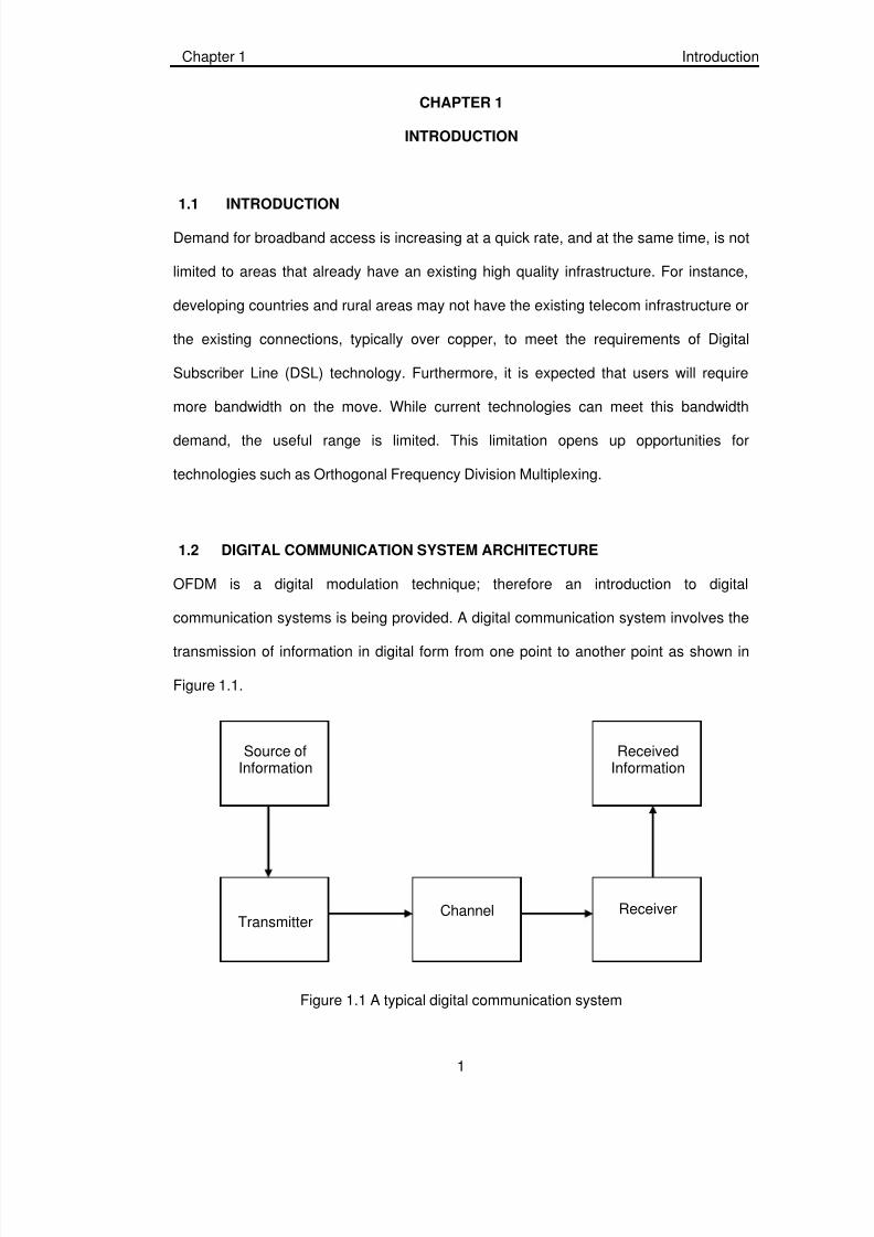
transmission of information in digital form from one point to another point as shown in
Figure 1.1.
Figure 1.1 A typical digital communication system
Source ofInformation
TransmitterChannel Receiver
ReceivedInformation

7/21/2019 FYP Final Report-libre
http://slidepdf.com/reader/full/fyp-final-report-libre 12/109
Chapter 1 Introduction
2
The three basic elements in a communication system are transmitter, channel and
receiver. The source of information is the messages that are to be transmitted to the
other end in the receiver. A transmitter can consist of source encoder, channel coder
and modulation. Source encoder provides an efficient representation of the information
through which the resources are conserved. A channel coder may include error
detection and correction code. A modulation process then converts the base band signal
into band pass signal before transmission.
During transmission, the signal experiences impairment which attenuates the signals
amplitude and distort signals phase. Also, the signals transmitting through a channel
also impaired by noise, which is assumed to be Gaussian distributed component.
At the receiving end, the reversed order of the steps taken in the transmitter is
performed. Ideally, the same information must be decoded at the receiving end.
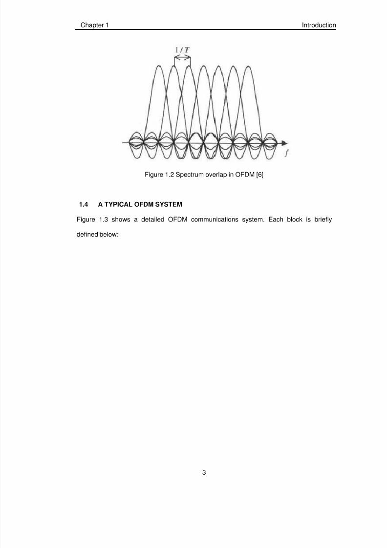
1.3 ORTHOGONAL FREQUENCY DIVISION MULTIPLEXING
Orthogonal frequency division multiplexing (OFDM) is a multi-carrier digital modulation
technique that has been recognized as an excellent method for high speed bi-directional
wireless data communication. OFDM effectively squeezes multiple modulated carriers
tightly together, reducing the required bandwidth but keeping the modulated signals
orthogonal so they do not interfere with each other.
OFDM is similar to FDM but much more spectrally efficient by spacing the sub-channels
much closer together (until they are actually overlapping)[1]. This is done by finding
frequencies that are orthogonal, which means that they are perpendicular in a
mathematical sense, allowing the spectrum of each sub-channel to overlap another
without interfering with it. In Figure 1.2 the effect of this is seen, as the required
bandwidth is greatly reduced by removing guard bands (which are present in FDM) and
allowing signals to overlap.
7/21/2019 FYP Final Report-libre
http://slidepdf.com/reader/full/fyp-final-report-libre 13/109
Chapter 1 Introduction
3
Figure 1.2 Spectrum overlap in OFDM [6]
1.4 A TYPICAL OFDM SYSTEM
Figure 1.3 shows a detailed OFDM communications system. Each block is briefly
defined below:

7/21/2019 FYP Final Report-libre
http://slidepdf.com/reader/full/fyp-final-report-libre 14/109
Chapter 1 Introduction
4
Figure 1.3 Complete OFDM system
1.4.1 SCRAMBLER / DESCRAMBLER
Data bits are given to the transmitter as inputs. These bits pass through a scrambler that
randomizes the bit sequence. This is done in order to make the input sequence more
!
!
"

7/21/2019 FYP Final Report-libre
http://slidepdf.com/reader/full/fyp-final-report-libre 15/109
Chapter 1 Introduction
5
disperse so that the dependence of input signal’s power spectrum on the actual
transmitted data can be eliminated [2].
At the receiver end descrambling is the last step. De-scrambler simply recovers original
data bits from the scrambled bits.
1.4.2 REED-SOLOMON ENCODER / DECODER
The scrambled bits are then fed to the Reed Solomon Encoder which is a part of
Forward Error Correction (FEC). Reed Solomon coding is an error-correction coding
technique. Input data is over-sampled and parity symbols are calculated which are then
appended with original data [3]. In this way redundant bits are added to the actual
message which provides immunity against severe channel conditions. A Reed Solomon
code is represented in the form RS (n, k), where
12 −=mn 1.1
t k m212 −−= 1.2
Here m is the number of bits per symbol, k is the number of input data symbols (to be
encoded), n is the total number of symbols (data + parity) in the RS codeword and t is
the maximum number of data symbols that can be corrected. At the receiver Reed
Solomon coded symbols are decoded by removing parity symbols.
1.4.3 CONVOLUTIONAL ENCODER / DECODER
Reed Solomon error-coded bits are further coded by Convolutional encoder. This coder
adds redundant bits as well. In this type of coding technique each m bit symbol is
transformed into an n bit symbol; m/n is known as the code rate. This transformation of
m bit symbol into n bit symbol depends upon the last k data symbols, therefore k is
known as the constraint length of the Convolutional code [4].

7/21/2019 FYP Final Report-libre
http://slidepdf.com/reader/full/fyp-final-report-libre 16/109
Chapter 1 Introduction
6
Viterbi algorithm is used to decode convolutionaly encoded bits at the receiver side.
Viterbi decoding algorithm is most suitable for Convolutional codes with k10.
1.4.4 INTERLEAVER / DE-INTERLEAVER
Interleaving is done to protect the data from burst errors during transmission.
Conceptually, the in-coming bit stream is re-arranged so that adjacent bits are no more
adjacent to each other. The data is broken into blocks and the bits within a block are re-
arranged [5]. Talking in terms of OFDM, the bits within an OFDM symbol are re-
arranged in such a fashion so that adjacent bits are placed on non-adjacent sub-carriers.
As far as De-Interleaving is concerned, it again rearranges the bits into original form
during reception.
1.4.5 CONSTELLATION MAPPER / DE-MAPPER
The Constellation Mapper basically maps the incoming (interleaved) bits onto different
sub-carriers. Different modulation techniques can be employed (such as QPSK, BPSK,
QAM etc.) for different sub-carriers. The De-Mapper simply extracts bits from the
modulated symbols at the receiver.
1.4.6 INVERSE FAST FOURIER TRANSFORM / FAST FOURIER TRANSFORM
This is the most important block in the OFDM communication system. It is IFFT that
basically gives OFDM its orthogonality [1]. The IFFT transform a spectrum (amplitude
and phase of each component) into a time domain signal. It converts a number of
complex data points into the same number of points in time domain. Similarly, FFT at the
receiver side performs the reverse task i.e. conversion from time domain back to
frequency domain.
7/21/2019 FYP Final Report-libre
http://slidepdf.com/reader/full/fyp-final-report-libre 17/109
Chapter 1 Introduction
7
1.4.7 ADDITION / REMOVAL OF CYCLIC PREFIX
In order to preserve the sub-carrier orthogonality and the independence of subsequent
OFDM symbols, a cyclic guard interval is introduced. The guard period is specified in
terms of the fraction of the number of samples that make up an OFDM symbol. The
cyclic prefix contains a copy of the end of the forthcoming symbol. Addition of cyclic
prefix results in circular convolution between the transmitted signal and the channel
impulse response. Frequency domain equivalent of circular convolution is simply the
multiplication of transmitted signal’s frequency response and channel frequency
response, therefore received signal is only a scaled version of transmitted signal (in
frequency domain), hence distortions due to severe channel conditions are eliminated
[6]. Removal of cyclic prefix is then done at the receiver end and the cyclic prefix–free
signal is passed through the various blocks of the receiver.
1.5 FIELD PROGRAMMABLE GATE ARRAY
By modern standards, a logic circuit with 20000 gates is common. In order to implement
large circuits, it is convenient to use a type of chip that has a large logic capacity. A field-
programmable gate arrays (FPGA) is a programmable logic device that support
implementation of relatively large logic circuits [6]. FPGA is different from other logic
technologies like CPLD and SPLD because FPGA does not contain AND or OR planes.
Instead, FPGA consists of logic blocks for implementing required functions.
An FPGA contains 3 main types of resources: logic blocks, I/O blocks for connecting to
the pins of the package, and interconnection wires and switches. The logic blocks are
arranged in a two-dimensional array, and the interconnection wires are organized as
horizontal and vertical routing channels between rows and columns of logic blocks [7].
The routing channels contain wires and programmable switches that allow the logic
blocks to be interconnected in many ways. FPGA can be used to implement logic
circuits of more than a few hundred thousands equivalent gates in size [7]. Equivalent

7/21/2019 FYP Final Report-libre
http://slidepdf.com/reader/full/fyp-final-report-libre 18/109
Chapter 1 Introduction
8
gates is a way to quantify a circuit’s size by assuming that the circuit is to be built using
only simple logic gate and then estimating how many of these gates are needed.
Figure 1.4 gives a clear picture of the FPGA design flow.
Figure 1.4 FPGA design flow [7]
1.6 PROJECT OBJECTIVE
The objective of this project is to carry out an efficient implementation of the OFDM
system (i.e. transmitter and receiver) using “Field Programmable Gate Array (FPGA)”.
FPGA has been chosen as the target platform because OFDM has large arithmetic
processing requirements which can become prohibitive if implemented in software on a
Digital Signal Processor (DSP) [7]. However, the highly pipelined nature of much of the
processing lends itself well to a hardware implementation. In addition, FPGA
implementation has the added advantage of allowing late modifications in response to
real world performance evaluation.
1.7 PROJECT SPECIFICATIONS
The complete OFDM system, comprising of the transmitter and the receiver, has been
implemented on a single FPGA board. The overall specifications are as follows:
7/21/2019 FYP Final Report-libre
http://slidepdf.com/reader/full/fyp-final-report-libre 19/109
Chapter 1 Introduction
9
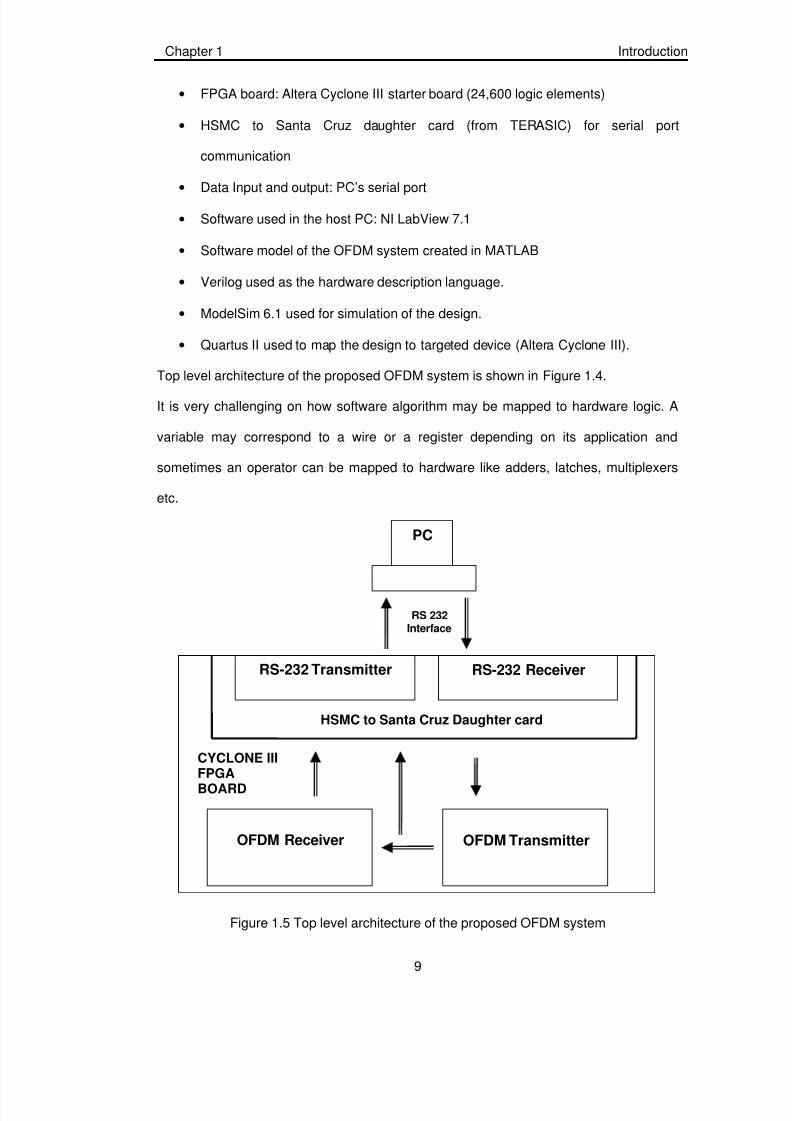
• FPGA board: Altera Cyclone III starter board (24,600 logic elements)
• HSMC to Santa Cruz daughter card (from TERASIC) for serial port
communication
• Data Input and output: PC’s serial port
• Software used in the host PC: NI LabView 7.1
• Software model of the OFDM system created in MATLAB
• Verilog used as the hardware description language.
• ModelSim 6.1 used for simulation of the design.
• Quartus II used to map the design to targeted device (Altera Cyclone III).
Top level architecture of the proposed OFDM system is shown in Figure 1.4.
It is very challenging on how software algorithm may be mapped to hardware logic. A
variable may correspond to a wire or a register depending on its application and
sometimes an operator can be mapped to hardware like adders, latches, multiplexers
etc.
Figure 1.5 Top level architecture of the proposed OFDM system
PC
RS-232 ReceiverRS-232 Transmitter
OFDM TransmitterOFDM Receiver
RS 232Interface
CYCLONE IIIFPGA
BOARD
HSMC to Santa Cruz Daughter card
7/21/2019 FYP Final Report-libre
http://slidepdf.com/reader/full/fyp-final-report-libre 20/109
Chapter 1 Introduction
10
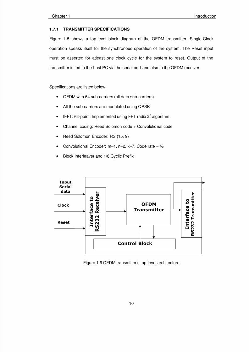
1.7.1 TRANSMITTER SPECIFICATIONS
Figure 1.5 shows a top-level block diagram of the OFDM transmitter. Single-Clock
operation speaks itself for the synchronous operation of the system. The Reset input
must be asserted for atleast one clock cycle for the system to reset. Output of the
transmitter is fed to the host PC via the serial port and also to the OFDM receiver.
Specifications are listed below:
• OFDM with 64 sub-carriers (all data sub-carriers)
• All the sub-carriers are modulated using QPSK
• IFFT: 64-point. Implemented using FFT radix 22 algorithm
• Channel coding: Reed Solomon code + Convolutional code
• Reed Solomon Encoder: RS (15, 9)
• Convolutional Encoder: m=1, n=2, k=7. Code rate = ½
• Block Interleaver and 1/8 Cyclic Prefix
Figure 1.6 OFDM transmitter’s top-level architecture
# $ #
%
&'
'
# $ #

7/21/2019 FYP Final Report-libre
http://slidepdf.com/reader/full/fyp-final-report-libre 21/109
Chapter 1 Introduction
11
1.7.2 RECEIVER SPECIFICATIONS
In figure 1.6 a top level block diagram of the receiver is shown. Its specifications are
same as that of the transmitter. Here the recovered (demodulated data would be fed to
the serial port.
Figure 1.7 OFDM receiver’s top-level architecture
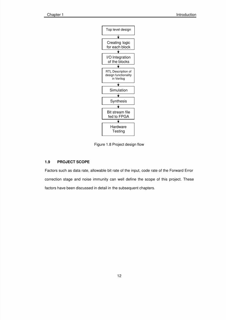
1.8 PROJECT DESIGN FLOW
The design procedure consists of following steps:
• Creating a top level design of the complete system
• Determining the basic operation of each block and creating the appropriate logic
• I/O integration of the various logic blocks
• Description of design functionality using Verilog hardware description language
• Modelsim is used to simulate the design functionality and to report errors in
desired behavior of the design
• Synthesis of the defined hardware is done which includes slack optimization,
power optimizations followed by placement and routing
• FPGA bitstream file is fed to the hardware
• Input is given to the system through the PC’s RS232 and hardware is tested
%
# $ #
%
&'
'
7/21/2019 FYP Final Report-libre
http://slidepdf.com/reader/full/fyp-final-report-libre 22/109
Chapter 1 Introduction
12
Figure 1.8 Project design flow
1.9 PROJECT SCOPE
Factors such as data rate, allowable bit rate of the input, code rate of the Forward Error
correction stage and noise immunity can well define the scope of this project. These
factors have been discussed in detail in the subsequent chapters.
Top level design
Creating logicfor each block
I/O Integrationof the blocks
RTL Description ofdesign functionality
in Verilog
Simulation
Synthesis
Bit stream filefed to FPGA
HardwareTesting
7/21/2019 FYP Final Report-libre
http://slidepdf.com/reader/full/fyp-final-report-libre 23/109
Chapter 2 Literature Survey
13
CHAPTER TWO
LITERATURE SURVEY
2.1 EVOLUTION OF OFDM
OFDM can be viewed as a collection of transmission techniques. When this technique is
applied in wireless environment, it is referred to as OFDM. In the wired environment,
such as asymmetric digital subscriber lines (ADSL), it is referred as discrete multi tone
(DMT). In OFDM, each carrier is orthogonal to all other carriers. However, this condition
is not always maintained in DMT [8]. OFDM is an optimal version of multi carrier
transmission schemes.
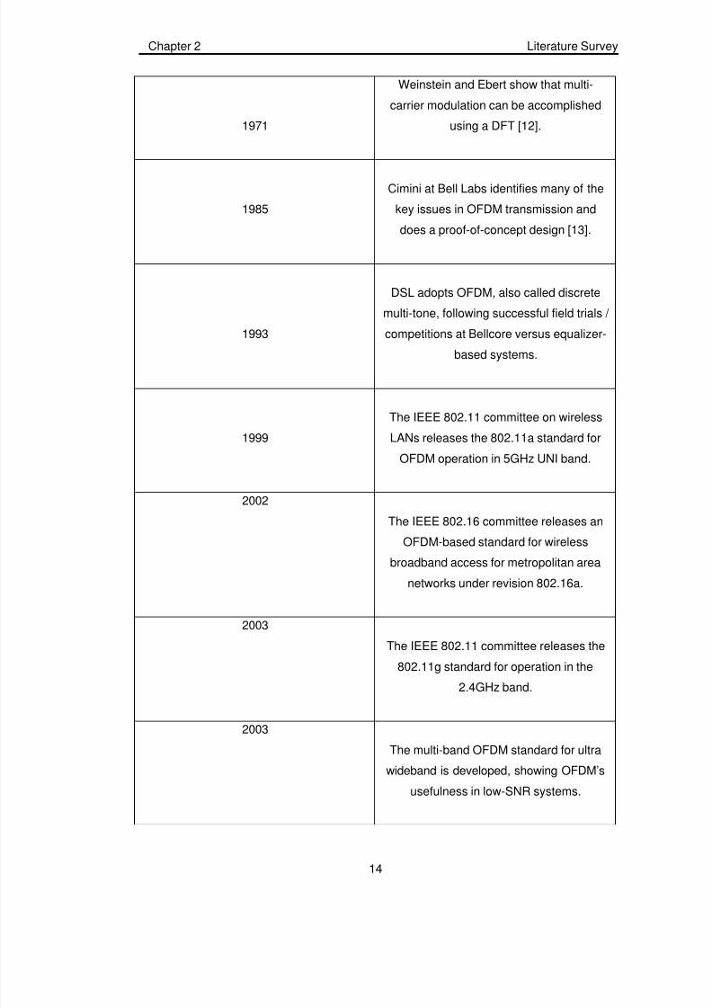
2.1.1 HISTORY OF OFDM
Although OFDM has become widely used only recently, the concept dates back some
40 years. Following table cites some landmark dates in the history of OFDM.
Table 2.1 A Brief History of OFDM
Year Event
1966
Chang shows that multi-carrier modulation
can solve the Multipath problem without
reducing data rate [10]. This is generally
considered the first official publication on
multi-carrier modulation. Some earlier work
was Holsinger’s 1964 MIT dissertation [9]
and some of Gallager’s early work on
waterfilling [11].
7/21/2019 FYP Final Report-libre
http://slidepdf.com/reader/full/fyp-final-report-libre 24/109
Chapter 2 Literature Survey
14
1971
Weinstein and Ebert show that multi-
carrier modulation can be accomplished
using a DFT [12].
1985
Cimini at Bell Labs identifies many of the
key issues in OFDM transmission and
does a proof-of-concept design [13].
1993
DSL adopts OFDM, also called discrete
multi-tone, following successful field trials /
competitions at Bellcore versus equalizer-
based systems.
1999
The IEEE 802.11 committee on wireless
LANs releases the 802.11a standard for
OFDM operation in 5GHz UNI band.
2002
The IEEE 802.16 committee releases an
OFDM-based standard for wireless
broadband access for metropolitan area
networks under revision 802.16a.
2003
The IEEE 802.11 committee releases the
802.11g standard for operation in the
2.4GHz band.
2003
The multi-band OFDM standard for ultra
wideband is developed, showing OFDM’s
usefulness in low-SNR systems.
7/21/2019 FYP Final Report-libre
http://slidepdf.com/reader/full/fyp-final-report-libre 25/109
Chapter 2 Literature Survey
15
Frequency Division Multiplexing (FDM) is also a form of the multi-channel transmission.
The use of Frequency Division Multiplexing (FDM) goes back over a long period of time,
where more than one low rate signal, such as telegraph, was carried over a relatively
wide bandwidth channel using a separate carrier frequency for each signal [1]. To
facilitate separation of the signals at the receiver, the carrier frequencies were spaced
sufficiently far apart so that the signal spectra did not overlap. Empty spectral regions
between the signals assured that they could be separated with readily realizable filters.
The resulting spectral efficiency was therefore quite low.
2.2 THE OFDM SYSTEM
A detailed explanation of the OFDM system was given in the previous chapter, in which
different building blocks of an OFDM communication system were discussed. Following
is a brief review of those concepts.
In 1971 Discrete Fourier Transform (DFT) was used in baseband
modulation/demodulation in order to achieve orthogonality7. Since DFT has heavy
computational requirements, therefore, Fast Fourier Transform (FFT) was utilized. For
an N point discrete Fourier Transform the required number of computations is N 2, but
that for FFT is Nlog (N), which is much lesser than DFT. In this way the problem of
bandwidth inefficiency due to the placement of guard bands between sub-channels was
solved and a new technique “Orthogonal Frequency Division Multiplexing” came into
being.
As OFDM is a multi-carrier modulation technique, therefore, the input data is split and
mapped onto different sub-carriers. Each carrier is modulated using one of the single-
carrier modulation techniques discussed above.
The OFDM system successfully avoids any inter-channel interference (ICI) because the
carriers are kept orthogonal. In addition, a cyclic prefix (CP) is added before the start of
each transmitted symbol to act as a guard period preventing inter-symbol interference
7/21/2019 FYP Final Report-libre
http://slidepdf.com/reader/full/fyp-final-report-libre 26/109
Chapter 2 Literature Survey
16
(ISI), provided that the delay spread in the channel is less than the guard period [17].
This guard period is specified in terms of the fraction of the number of samples that
make up a symbol.
2.3 ADVANTAGES AND DISADVANTAGES OF OFDM
Another advantage of OFDM is its resilience to Multipath, which is the effect of multiple
reflected signals hitting the receiver. This results in interference and frequency-selective
fading which OFDM is able to overcome by utilizing its parallel, slower bandwidth nature.
This makes OFDM ideal to handle the harsh conditions of the mobile wireless
environment.
The introduction of cyclic prefix made OFDM system resistant to time dispersion [18].
OFDM symbol rate is low since a data stream is divided into several parallel streams
before transmission. This make the fading is slow enough for the channel to be
considered as constant during one OFDM symbol interval.
Cyclic prefix is a crucial feature of OFDM used to combat the inter-symbol interference
(ISI) and inter-channel-interference (ICI) introduced by the multi-path channel through
which the signal is propagated [1]. The basic idea is to replicate part of the OFDM time-
domain waveform from the back to the front to create a guard period. The duration of the
guard period should be longer than the worst-case delay spread of the target multi-path
environment. The use of a cyclic prefix instead of a plain guard interval, simplifies the
channel equalization in the demodulator.
In wire system, OFDM system can offer an efficient bit loading technique [1]. It enables a
system to allocate different number of bits to different sub channels based on their
individual SNR. Hence, an efficient transmission can be achieved.
One of the major disadvantages of OFDM is its requirement for high peak-to average-
power ratio (PAPR) [6]. This put high demand on linearity in amplifiers.

7/21/2019 FYP Final Report-libre
http://slidepdf.com/reader/full/fyp-final-report-libre 27/109
Chapter 2 Literature Survey
17
Second, the synchronization error can destroy the orthogonality and cause interference.
Phase noise error and Doppler shift can cause degradation to OFDM system [1]. A lot of
effort is required to design accurate frequency synchronizers for OFDM.
OFDM’s high spectral efficiency and resistance to Multipath make it an extremely
suitable technology to meet the demands of wireless data traffic. This has made it not
only ideal for such new technologies like WiMAX and Wi-Fi but also currently one of the
prime technologies being considered for use in future fourth generation (4G) networks.
2.4 APPLICATIONS OF OFDM
Initially, OFDM applications are scarce because of their implementation complexity.
Now, OFDM has been adopted as the new European digital audio broadcasting (DAB)
standard and for terrestrial digital video broadcasting (DVB) [19].
In fixed-wire applications, OFDM is employed in asynchronous digital subscriber line
(ADSL) and high bit-rate digital subscriber line (HDSL) systems. It has been proposed
for power line communications systems as well due to its resilience to dispersive
channel and narrow band interference. It has been employed in WiMAX a well.
2.5 VERILOG HARDWARE DESCRIPTION LANGUAGE
Verilog HDL is one of the two most common Hardware Description Languages (HDL)
used by integrated circuit (IC) designers. The other one is VHDL.
HDL allows the design to be simulated earlier in the design cycle in order to correct
errors or experiment with different architectures. Designs described in HDL are
technology-independent, easy to design and debug, and are usually more readable than
schematics, particularly for large circuits.
Verilog can be used to describe designs at four levels of abstraction [20]:
(i) Algorithmic level (much like c code with if, case and loop statements).
(ii) Register transfer level (RTL uses registers connected by Boolean equations).
(iii) Gate level (interconnected AND, NOR etc.).

7/21/2019 FYP Final Report-libre
http://slidepdf.com/reader/full/fyp-final-report-libre 28/109
Chapter 2 Literature Survey
18
(iv) Switch level (the switches are MOS transistors inside gates).
The language also defines constructs that can be used to control the input and output of
simulation.
More recently Verilog is used as an input for synthesis programs which will generate a
gate-level description (a netlist) for the circuit. Some Verilog constructs are not
synthesizable. Also the way the code is written will greatly affect the size and speed of
the synthesized circuit.
2.6 SYNTHESIS PROCESS IN VERILOG HDL
Synthesis is to construct a gate-level net list from a model of a circuit described in
Verilog. The synthesis process is described in diagram below.
Figure 2.1 Synthesis Process in Verilog Environment
A synthesis program may generate an RTL net list, which consists of register-transfer
level blocks such as flip-flops, arithmetic-logic-units and multiplexers interconnected by
"(
)* %(
)
+( *
*"*
*
*
%(
7/21/2019 FYP Final Report-libre
http://slidepdf.com/reader/full/fyp-final-report-libre 29/109
Chapter 2 Literature Survey
19
wires. All these are performed by RTL module builder. This builder is to build or acquire
from a library predefined components, each of the required RTL blocks in the user-
specified target technology.
The above synthesis process may produce an unoptimized gate level net list. A logic
optimizer can use the produced net list and the constraint specified to produce an
optimized gate level net list. This net list can be programmed directly into a FPGA chip.

7/21/2019 FYP Final Report-libre
http://slidepdf.com/reader/full/fyp-final-report-libre 30/109
Chapter 3 Transmitter Design and Implementation
20
CHAPTER 3
TRANSMITTER DESIGN AND IMPLEMENTATION
3.1 INTRODUCTION
The proposed OFDM system consists of an OFDM baseband transmitter and an OFDM
baseband receiver. This chapter gives details on the complete architecture of the
proposed design and elaborates further on the design and implementation of the
transmitter portion of the project.
The transmitter gets its input from the serial port of the host PC. An input stream is sent
as input to the transmitter that modulates the incoming stream by splitting it and putting it
onto separate sub-carriers (64 in our case). The modulated data after passing through
various blocks is given as input to the receiver and also sent back to the host PC (via
serial port) for demonstration purposes.
3.2 OFDM SYSTEM HARDWARE ARCHITECTURE
Implementation of the proposed system has been done on Altera’s Cyclone III starter
board. This board does not have a serial port therefore we used an HSMC to Santa Cruz
daughter card (from TERASIC). This daughter card contains an Altera standard HSMC
connector and a serial port. The HSMC connector plugs into the HSMC connector
present on the Cyclone III board, thereby providing an RS232 physical connection to the
FPGA board.
An RS232 receiving module takes the serial stream and extracts the 8 bit payload by
removing the start and stop bits. Figure 3.1 shows the format of data stream in serial
communications (RS232 standard).
Figure 3.1 Serial communication format (8 bit data + start bit + stop bit)
StartStop D7 D6 D5 D4 D3 D2 D1 D0

7/21/2019 FYP Final Report-libre
http://slidepdf.com/reader/full/fyp-final-report-libre 31/109
Chapter 3 Transmitter Design and Implementation
21
The 1-byte data from the RS232 receiver is stored in a FIFO register. Data from the
FIFO is given (bit by bit) to the transmitter module. Figure 3.2 depicts the hardware
architecture of the project highlighting only the transmitter portion.
Figure 3.2 Complete Architecture of the proposed OFDM system (transmitter
highlighted)
O F D
M T
r a n s m i t t e r
HSMC TO
SANTA CRUZCONNECTOR
RS232Receiver
FIFO
Scrambler
RS Encoder
Conv. Encoder
Interleaver
Constellation mapper
IFFT
Cyclic Prefix
RS232 Transmitter
FIFO
H i g h S p e
e d M e z z a n i n e C o n n e c t o r
I n t e r f a c e
R S 2 3 2 p o r t
On board 50 MHz clock
PLL
OFDM Receiver
Input
C o n t r o l U n i t
Output
7/21/2019 FYP Final Report-libre
http://slidepdf.com/reader/full/fyp-final-report-libre 32/109
Chapter 3 Transmitter Design and Implementation
22
We can see that the modulated output from the transmitter is fed into another FIFO, and
then taken out into the RS232 transmitter (byte by byte) that prepares the data for serial
transmission over the RS232 interface by adding start and stop bits. The baud rate on
which the serial port is operating is 115.2 kbps.
There is a 50 MHz on-board clock source which in conjunction with the PLL core
(provided with the Quartus II software) can be used to produce any clock frequency. The
output of the PLL then provides clock(s) to all the modules.
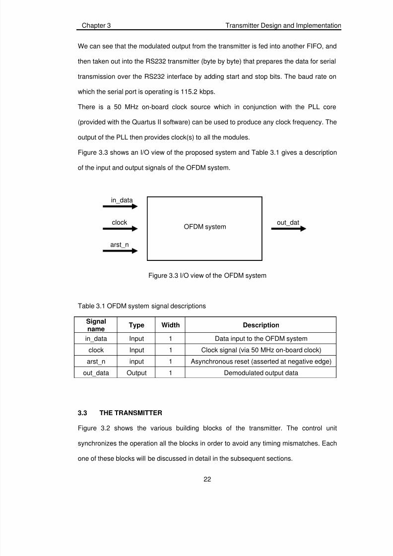
Figure 3.3 shows an I/O view of the proposed system and Table 3.1 gives a description
of the input and output signals of the OFDM system.
Figure 3.3 I/O view of the OFDM system
Table 3.1 OFDM system signal descriptions
Signalname
Type Width Description
in_data Input 1 Data input to the OFDM system
clock Input 1 Clock signal (via 50 MHz on-board clock)
arst_n input 1 Asynchronous reset (asserted at negative edge)
out_data Output 1 Demodulated output data
3.3 THE TRANSMITTER
Figure 3.2 shows the various building blocks of the transmitter. The control unit
synchronizes the operation all the blocks in order to avoid any timing mismatches. Each
one of these blocks will be discussed in detail in the subsequent sections.
OFDM system
in_data
clock
arst_n
out_dat

7/21/2019 FYP Final Report-libre
http://slidepdf.com/reader/full/fyp-final-report-libre 33/109
Chapter 3 Transmitter Design and Implementation
23
As mentioned above, the transmitter gets its input from the FIFO register one bit per
clock cycle. This implies that the input to the transmitter is I bit wide. It is only when the
FIFO is full that the transmitter starts extracting data from it. Similarly when the FIFO
gets empty the transmitter stops taking data from it. Therefore, the transmitter makes
use of certain control and status signals provided by the FIFO to determine when to ask
the FIFO for data and when to stop taking input data.
In a similar fashion, the output of the transmitter is also stored in a FIFO register. In
order for this FIFO to determine when to start storing output data from the transmitter,
the transmitter provides a status signal that tells this FIFO that data is present on the
output lines.
Figure 3.4 shows the I/O diagram for the transmitter and Table 3.2 gives the description
of the signals in and out of the transmitter.
Figure 3.4 I/O diagram of the transmitter
Table 3.2 Transmitter signal descriptions
SignalName
Type Width Description
in_data Input 1 Input data to the transmitter
clock Input 1 Clock – 20 MHz (output of PLL)
arst_n Input 1 Asynchronous reset (asserted on negative
Transmitter
out_dat
in_data
readempty
wrfull
arst_n
clock
readreq
start_output
7/21/2019 FYP Final Report-libre
http://slidepdf.com/reader/full/fyp-final-report-libre 34/109
Chapter 3 Transmitter Design and Implementation
24
edge)
wrfull Input 1FIFO status signals - asserted when FIFO is
full
readempty Input 1FIFO status signal – asserted when FIFO is
empty
out_data Output 48 Modulated data coming out of the transmitter
readreq Output 1FIFO control signal – requests data from FIFO(transmitter asserts this signal when the FIFO
is full)
start_output Output 1Asserted when there is data present on the
out_data lines
3.4 FIFO
First In First Out is a popular data structure (also known as queue) that is used for
buffering in order to provide flow control. We obtained the FIFO from Altera’s
Megafunction Wizard (Quartus II). This parameterized Megafunction allows creating
FIFOs of any width and depth with various options of control and status signals. Using
technology specific modules allows for quick prototyping of the design. Hence all we had
to do was to provide appropriate parameters and interface the Megafunction in our
design.
Now the following sections describe the various building blocks of the OFDM transmitter
as shown in Figure 3.2. The functions of these blocks and their role in the OFDM system
were briefly discussed in Chapter 1, therefore here the hardware implementation details
of these blocks are being discussed
3.5 SCRAMBLER
A scrambler (often referred to as a randomizer) is a device that manipulates a data
stream before transmitting. The purpose of scrambling is to eliminate the dependence of
a signal’s power spectrum upon the actual transmitted data and making it more disperse
to meet maximum power spectral density requirements, because if the power is
concentrated in a narrow frequency band, it can interfere with adjacent channels [14].

7/21/2019 FYP Final Report-libre
http://slidepdf.com/reader/full/fyp-final-report-libre 35/109
Chapter 3 Transmitter Design and Implementation
25
3.5.1 DESIGN OF SCRAMBLER
Figure 3.1 shows the input/output parameters of the Scrambler. Input bus is 1 bit wide
and arst_n is the asynchronous reset input. A negative edge on the arst_n input resets
the Scrambler. A bit is latched in at the positive edge of the clock. See Table 3.3 for a
description of the signals.
Figure 3.5 Scrambler I/O diagram
Table 3.3 Scrambler signal descriptions
SignalName
Type Width Description
in Input 1 Input data to the transmitter
clock Input 1 Positive edge clockarst_n Input 1 Asynchronous reset (Negative edged)
enable Input 1 If high, input is present on the line in
out Output 1 Output scrambled data
Scramblers can be implemented using a Linear Feedback Shift Register (LFSR) [9]. An
LFSR is a simple register composed of memory elements (flip-flops) and modulo-2
adders (i.e. XOR gates). Feedback is taken from two or more memory elements, which
are XOR-ed and fed back to the first stage (memory element) of the LFSR. In the
proposed design, a standard 7 bit scrambler has been used to randomize the incoming
bits. An initial seed value is stored in the LFSR when arst_n is asserted; this value may
Scrambler out
In
clock
arst_n
enable
7/21/2019 FYP Final Report-libre
http://slidepdf.com/reader/full/fyp-final-report-libre 36/109
Chapter 3 Transmitter Design and Implementation
26
be any random bit string except for all zeroes or all ones. If the initial seed contains all
zeroes or all ones then the LFSR is locked in a state where every output value is same
i.e. either one or zero.
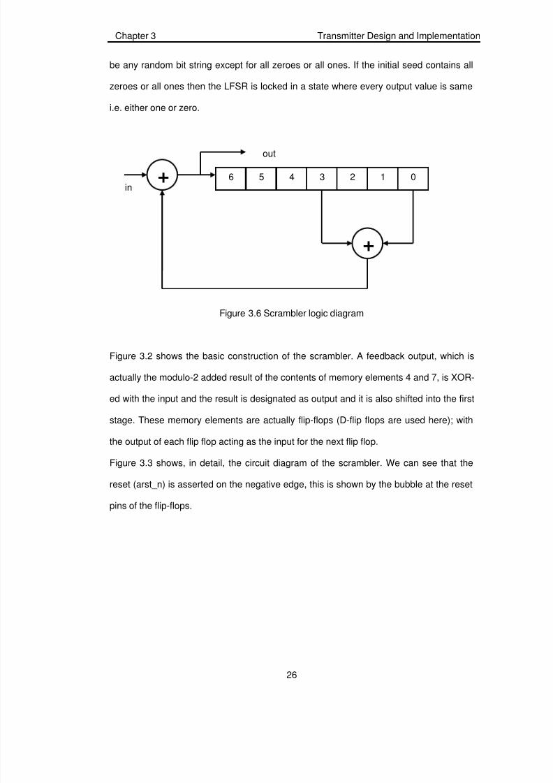
Figure 3.6 Scrambler logic diagram
Figure 3.2 shows the basic construction of the scrambler. A feedback output, which is
actually the modulo-2 added result of the contents of memory elements 4 and 7, is XOR-
ed with the input and the result is designated as output and it is also shifted into the first
stage. These memory elements are actually flip-flops (D-flip flops are used here); with
the output of each flip flop acting as the input for the next flip flop.
Figure 3.3 shows, in detail, the circuit diagram of the scrambler. We can see that the
reset (arst_n) is asserted on the negative edge, this is shown by the bubble at the reset
pins of the flip-flops.
6 5 4 3 2 1 0
,
,
out
in

7/21/2019 FYP Final Report-libre
http://slidepdf.com/reader/full/fyp-final-report-libre 37/109
Chapter 3 Transmitter Design and Implementation
27
Figure 3.7 Circuit diagram of Scrambler
3.6 REED SOLOMON ENCODER
Reed Solomon forward error correcting codes have become commonplace in modern
digital communications. Although invented in 1960 by Irving Reed and Gustave
Solomon, then working at MIT Lincoln Labs [21], it was many years before technology
caught up and was able to provide efficient hardware implementations.
Versions of Reed Solomon codes are now used in error correction systems found just
about everywhere, including [232:
• Storage devices (hard disks, compact disks, DVD, barcodes)
• Wireless communications (mobile phones, microwave links)
• Digital television Satellite communications (including deep space missions like
Voyager)
• Broadband modems (ADSL, xDSL etc)
3.6.1 DESCRIPTION OF THE REED SOLOMON CODE
Reed Solomon codes work by adding extra information (redundancy) to the original
data. The encoded data can then be stored or transmitted. When the encoded data is
D Q D Q D Q D Q D Q D Q D Q
clockarst_n
in
out
7/21/2019 FYP Final Report-libre
http://slidepdf.com/reader/full/fyp-final-report-libre 38/109
Chapter 3 Transmitter Design and Implementation
28
recovered it may have errors introduced, for instance by scratches on the CD,
imperfections on a hard disk surface or radio frequency interference with mobile phone
reception. The added redundancy allows a decoder (with certain restrictions) to detect
which parts of the received data are corrupted, and correct them [22]. The number of
errors the code can correct depends on the amount of redundancy added.
RS codes are a systematic linear block code. It is a block code because the code is put
together by splitting the original message into fixed length blocks. Each block is further
sub divided into m-bit symbols [22]. Each symbol is a fixed width, usually 3 to 8 bits
wide. In the proposed design, each symbol is 4 bits wide.
The linear nature of the codes ensures that in practice every possible m-bit word is a
valid symbol. For instance with an 4-bit code all possible 4 bit words are valid for
encoding, and you don't have to worry about what data you are transmitting. Systematic
means that the encoded data consists of the original data with the extra 'parity' symbols
appended to it [22].
An RS code is partially specified as an RS (n, k) with m-bit symbols, where
12 −=
m
n 3.1
t k m212 −−= 3.2
2
)( k nt
−= 3.3
where m is the number of bits per symbol, k is the number of input data symbols (to be
encoded), n is the total number of symbols (data + parity) in the RS codeword and t is
the maximum number of data symbols that can be corrected. The difference n-k (usually
called 2t) is the number of parity symbols that have been appended to make the
encoded block.
In the proposed design n=15 and k=9 represented by RS (15, 9). It gives m=4 and t=3.
Therefore, each symbol is 4 bits wide and a maximum of 3 symbols can be corrected in

7/21/2019 FYP Final Report-libre
http://slidepdf.com/reader/full/fyp-final-report-libre 39/109
Chapter 3 Transmitter Design and Implementation
29
the decoder. Figure 3.4 graphically represents an n symbol code showing the parity and
data portions.
Figure 3.8 RS (n, k) code
The power of Reed Solomon codes lies in being able to just as easily correct a
corrupted symbol with a single bit error as it can correct a symbol with all its bits in
error. This makes RS codes particularly suitable for correcting burst errors. Usually the
encoded data is transmitted or stored as a sequence of bits. In the proposed design
upto 12 bits could be corrupted affecting at most 3 symbols, and the original message
could still be recovered.
However it does mean that RS codes are relatively sensitive to evenly spaced errors.
3.6.2 GALOIS FIELD ARITHMETIC
Reed Solomon codes are based on finite fields, often called Galois fields. Rather than
look at individual numbers and equations, the approach of modern mathematicians is to
look at all the numbers that can be obtained from some given initial collection by using
operators such as addition, subtraction, multiplication and division. The resulting
collection is called a field. Some fields, like the set of integers, are infinite.
Galois fields have the useful property that any operation on an element of the field will
always result in another element of the field [23]. The field is also finite, so it can be
fully represented by a fixed length binary word. An arithmetic operation that, in
traditional mathematics, results in a value out of the field gets mapped back in to the
field - it's a form of modulo arithmetic [23].
Original data symbols Parity
n symbols
7/21/2019 FYP Final Report-libre
http://slidepdf.com/reader/full/fyp-final-report-libre 40/109
Chapter 3 Transmitter Design and Implementation
30
Galois arithmetic has very little to do with counting things, 2+2 is not necessarily 4. For
ease of handling the Galois field elements are often called by their binary equivalent,
but this can be misleading. There are many Galois fields, and part of the RS
specification is to define which field is used.
Galois arithmetic is ideally suited to hardware implementation [23]. Addition and
subtraction consists of simply XORing two symbols together. Multiplication is a little
more difficult, (as always) but can be done using purely combinational logic.
An RS code with 4 bit symbols will use a Galois field GF (24), consisting of 16 symbols.
Thus every possible 4 bit value is in the field. The order in which the symbols appear
depends on the primitive polynomial [23]. This polynomial is used in a simple iterative
algorithm to generate each element of the field. Different polynomials will generate
different fields. The primitive polynomial used in the proposed design for GF (2 4) is,
41)( X X X P ++= 3.4
The elements of the Galois field GF (24) are generated by using this primitive
polynomial. The symbol is used to give the power representation of each element.
Table 3.4 Elements of GF (24) and their binary equivalents
Power Representation Binary representation
0 0000
0 1000
1 0100
2 0010
3 0001
4 1100
5 0110
6 0011
7 1101
8 1010
9 0101
10 1110
11 0111
12 1111

7/21/2019 FYP Final Report-libre
http://slidepdf.com/reader/full/fyp-final-report-libre 41/109
Chapter 3 Transmitter Design and Implementation
31
13 1011
14 1001
These values are calculated by substituting for X in the primitive polynomial such that,
α α += 14
3.5
This will give the value of 4, and for the value of 5 we write,
α α α 45
= 3.6
α α α )1(5
+= 3.7
25α α α += 3.8
Similarly the rest of the elements are calculated.
The final parameter that is used to generate RS codes is the generator polynomial [23].
This polynomial is of order 2t (6 in our case). It is obtained as follows,
))......()()()(()(2432 t
X X X X X X G α α α α α +++++= 3.9
For our case (i.e. RS (15, 9) and 2t=6) the generator polynomial turns out to be,
6510414342696)( X X X X X X X G ++++++= α α α α α α 3.10
Given n, k, the symbol width m, the Galois field primitive polynomial P and the
generator polynomial G, the Reed-Solomon code is fully specified.
7/21/2019 FYP Final Report-libre
http://slidepdf.com/reader/full/fyp-final-report-libre 42/109
Chapter 3 Transmitter Design and Implementation
32
3.6.3 ENCODER DESIGN
Since the code is systematic, the whole of the block can be read into the encoder, and
then output the other side without alteration. Once the kth data symbol has been read
in, the parity symbol calculation is finished, and the parity symbols can be output to give
the full n symbols.
The idea of the parity words is to create a long polynomial (n coefficients long – it
contains the message and the parity) which can be divided exactly by the RS generator
polynomial. That way, at the decoder the received message block can be divided by the
RS generator polynomial. If the remainder of the division is zero, then no errors are
detected. If there is a remainder, then there are errors. Dividing a polynomial by
another is not conceptually easy, but if you follow the mathematics in some of the
references it is not too hard to understand.
The encoder acts to divide the polynomial represented by the k message symbols D(x)
by the RS generator polynomial G(x).
Figure 3.5 (on next page) depicts the top level architecture of the proposed Reed
Solomon Encoder. This is a bit-serial Reed Solomon Encoder which means that its
input bus is one bit wide. One bit is latched per positive edge of the clock. Having 4 bits
per symbol makes it clear that 4 clock cycles are required to input a symbol. arst_n is
the same asynchronous reset signal as in Scrambler.
Table 3.5 Signal descriptions for Reed Solomon Encoder
SignalName
Type Width Description
in_data Input 1 Input data to the Reed Solomon Encoder
clock Input 1 Positive edge clock
arst_n Input 1 Asynchronous reset (Negative edged)
enable Input 1 If high, input is present on the line in_data
out Input 1 Output RS encoded data
7/21/2019 FYP Final Report-libre
http://slidepdf.com/reader/full/fyp-final-report-libre 43/109
Chapter 3 Transmitter Design and Implementation
33
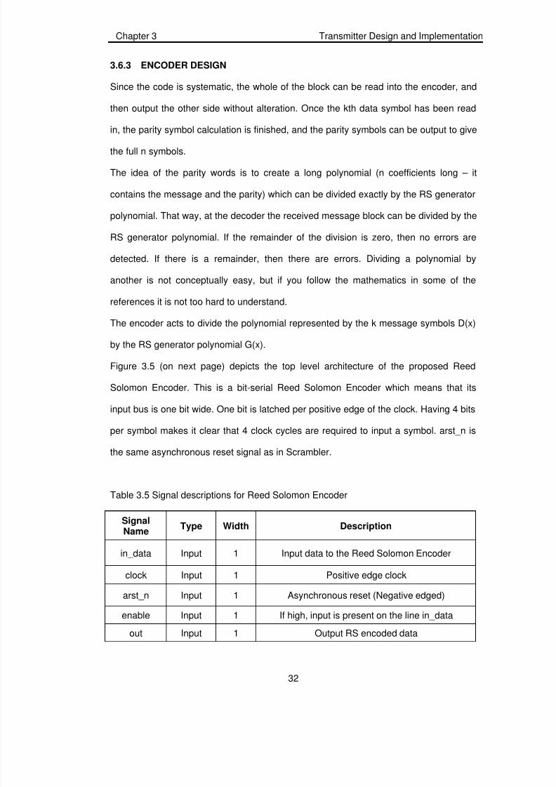
The encoder contains the following three building blocks (as shown in Figure 3.5):
• Shift Registers
• Galois field addition and multiplication
• Redundancy interval controller
Figure 3.9 Top-level structure of the Reed Solomon Encoder
This block contains 2t shift registers each m bits wide. Therefore, for our case there
would be 6 shift registers each 4 bits wide. One of these six registers has parallel
loading capability as well.
Figure 3.6 is a detailed architecture of Reed Solomon Encoder. It is seen that the reset
and clock signals are not shown. We can see the six shift registers. The output of each
register becomes the shift input of the next register stage. An exception is Reg5; its
output is XORed with the input data bit and then ANDed with the compliment of
redundancy interval bit (red), and then this output of the AND gate becomes the shift
input for Reg4. Outputs of these registers act as inputs for the Galois Field block
described next.
Shift Registers
Galois fieldaddition andmultiplication
RedundancyInterval
Controller
clock
in_data
arst_n
out

7/21/2019 FYP Final Report-libre
http://slidepdf.com/reader/full/fyp-final-report-libre 44/109
Chapter 3 Transmitter Design and Implementation
34
Figure 3.10 Detailed architecture of Reed Solomon Encoder
The Galois Field Adder and Multiplier block performs all the Galois Field arithmetic
functions. Figure 3.7 depicts the internal architecture of the GF multiplier and adder.
It works as follows: R0 to R5 are basically register outputs that are shifted out into the
GF circuit (as shown in figure 3.6). This circuit basically multiplies contents of each
register with a constant multiplier which is established by connections to the XOR gates.
For instance, R1 is connected to 2nd and 4th XOR gates so R1 is multiplied by 0101
which is 9 and is also a coefficient of the generator polynomial. In this way every
register is multiplied by the corresponding coefficient of the generator polynomial. Hence
after these multiplications the products are added. This process takes four clock cycles
and in the fourth cycle the result is loaded into R5 as shown in figure 3.6.
Reg5 Reg4 Reg3 Reg2 Reg1 Reg0
GF Multiplier and Adder
-
MUX.
)
Redundancyinterval controller
out
red red
in_data

7/21/2019 FYP Final Report-libre
http://slidepdf.com/reader/full/fyp-final-report-libre 45/109
Chapter 3 Transmitter Design and Implementation
35
Figure 3.11 Galois Field multiplier and adder
Figure 3.6 shows how the Redundancy interval controller is connected to the main
circuit. For the first 36 clock cycles (9x4) the redundancy signal (given the name red in
figure 3.6) is low and data bits go into the circuit and through the multiplexer as well.
But after that the red signal goes high allowing the parity bits to pass through the
multiplexer. Redundancy is the name given to the interval during which data bits are not
allowed to get into the circuit and parity bits are brought out. To achieve this, a 6-bit
counter is employed. Using this counter a high output is obtained when the counter
counts 36 and it is brought back to low when it counts 60 (36+24).
3.7 CONVOLUTIONAL ENCODER
Convolutional coding is part of the Forward Error Correction (FEC) done in
communication systems. The purpose of forward error correction (FEC) is to improve the
capacity of a channel by adding some carefully designed redundant information to the
data being transmitted through the channel [4]. The process of adding this redundant
information is known as channel coding [4]. Convolutional codes operate on serial data,
one or a few bits at a time. There are a variety of useful Convolutional, and a variety of
D0D1D2D3
.-#$
/0
7/21/2019 FYP Final Report-libre
http://slidepdf.com/reader/full/fyp-final-report-libre 46/109
Chapter 3 Transmitter Design and Implementation
36
algorithms for decoding the received coded information sequences to recover the
original data.
Convolutional codes are usually described using two parameters: the code rate and the
constraint length. The code rate, m/n, is expressed as a ratio of the number of bits into
the Convolutional encoder (m) to the number of channel symbols output by the
Convolutional encoder (n) in a given encoder cycle. The constraint length parameter, K,
denotes the "length" of the Convolutional encoder, i.e. how many k-bit stages are
available to feed the combinatorial logic that produces the output symbols. Convolutional
codes are often used to improve the performance of digital radio, mobile phones, and
satellite links.
In the proposed design a Convolutional encoder with a code rate of ½ has been chosen
i.e. m=1 and n=2. A constraint length of 7 is kept because it is standard and its decoding
can be efficiently done using the popular “Viterbi Decoding Algorithm”.
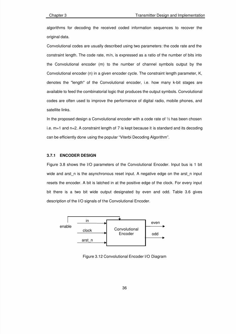
3.7.1 ENCODER DESIGN
Figure 3.8 shows the I/O parameters of the Convolutional Encoder. Input bus is 1 bit
wide and arst_n is the asynchronous reset input. A negative edge on the arst_n input
resets the encoder. A bit is latched in at the positive edge of the clock. For every input
bit there is a two bit wide output designated by even and odd. Table 3.6 gives
description of the I/O signals of the Convolutional Encoder.
Figure 3.12 Convolutional Encoder I/O Diagram
Convolutional
Encoder
evenin
clock
arst_nodd
enable
7/21/2019 FYP Final Report-libre
http://slidepdf.com/reader/full/fyp-final-report-libre 47/109
Chapter 3 Transmitter Design and Implementation
37
Table 3.6 Signal descriptions for Convolutional Encoder
SignalName
Type Width Description
in Input 1 Input data to the Convolutional Encoder
clock Input 1 Positive edge clock
arst_n Input 1 Asynchronous reset (Negative edged)
Enable Input 1 If high, input is present on the line in
even Output 1 Least significant bit of the output
odd Output 1 Most significant bit of the output
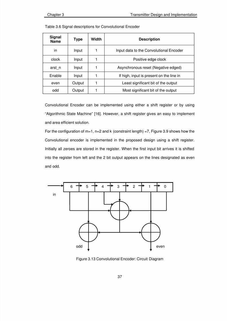
Convolutional Encoder can be implemented using either a shift register or by using
“Algorithmic State Machine” [16]. However, a shift register gives an easy to implement
and area efficient solution.
For the configuration of m=1, n=2 and k (constraint length) =7, Figure 3.9 shows how the
Convolutional encoder is implemented in the proposed design using a shift register.
Initially all zeroes are stored in the register. When the first input bit arrives it is shifted
into the register from left and the 2 bit output appears on the lines designated as even
and odd.
Figure 3.13 Convolutional Encoder: Circuit Diagram
6 5 4 3 2 1 0
evenodd
in

7/21/2019 FYP Final Report-libre
http://slidepdf.com/reader/full/fyp-final-report-libre 48/109
Chapter 3 Transmitter Design and Implementation
38
The even output is generated by adding the contents of 1st, 0, 3 rd, 4 th and 6th stages of
the shift register, whereas the odd output is generated by adding the 5 th, 0, 3rd, 4th and
6th stages of the register. This addition is modulo-2 addition carried out through XOR
gates (modulo-2 addition is basically a XOR operation). Just like the Scrambler the
memory elements here are D-flip-flops as well.
3.8 INTERLEAVER
Interleaving is mainly used in digital data transmission technology, to protect the
transmission against burst errors. These errors overwrite a lot of bits in a row, but
seldom occur. The device that performs interleaving is known as Interleaver.
Conceptually, the in-coming bit stream is re-arranged so that adjacent bits are no more
adjacent to each other. Actually the data is broken into blocks and the bits within a block
are re-arranged. In the proposed design, a block consists of 64 symbols (128 bits).
Number of bits in each symbol depends upon the corresponding single-carrier
modulation technique to be applied to produce that symbol.
Figure 15 shows how an Interleaver is generally implemented [23]. Two memory
elements (usually RAMs) are used. In the first RAM the incoming block of bits is stored
in sequential order. This data from the first RAM is read out randomly (using an
algorithm) so that the bits are re-arranged and stored in the second RAM and then read
out.
Figure 3.14 Interleaving concept
As mentioned above that the incoming bit stream is broken into blocks, when
interleaving in the OFDM system the block size should be equal to the size of an OFDM
7/21/2019 FYP Final Report-libre
http://slidepdf.com/reader/full/fyp-final-report-libre 49/109
Chapter 3 Transmitter Design and Implementation
39
symbol. Since there are 64 sub-carriers and each sub-carrier is modulated using QPSK,
therefore in one OFDM symbol there would be 128 bits. Hence, the job of the interleaver
would be to re-arrange the bits within the OFDM symbol.
3.8.1 INTERLEAVER DESIGN
As discussed above, the function that the interleaver has to perform is to read 128 bits,
re-arrange them and read them out. This can be accomplished by using RAMs for
temporarily storing the bits and then the bits can be read out from the RAMs in the
desired order. Remember that the block before the interleaver is the Convolutional
Encoder that gives an output of two bits. Therefore the input bus of the interleaver
should be two bits wide.
Figure 3.15 Interleaver I/O diagram (A top-level architecture)
Figure 3.12 shows the top-level architecture of the interleaver.
Block Memory
Address ROM
Controller
in2
clock
arst_n
out
2
enable
7/21/2019 FYP Final Report-libre
http://slidepdf.com/reader/full/fyp-final-report-libre 50/109
Chapter 3 Transmitter Design and Implementation
40
Table 3.7 Signal descriptions for Interleaver
SignalName
Type Width Description
in Input 2 Input data to the Interleaver
clock Input 1 Positive edge clock
arst_n Input 1 Asynchronous reset (Negative edged)
enable Input 1 If high, input is present on the line in
out Output 2 Output of the interleaver
Note that the input and output buses are two bits wide. The three building blocks of the
interleaver are:
• Block Memory
• Controller
• Address ROM
The block memory contains the memory elements necessary to store the incoming block
of data. There are a total of four memory elements; each is a 64x1 RAM. Four RAMs are
used in order to achieve pipelined operation. Two of these RAMs are used for writing a
block while another block is being read out from the other two RAMs. In this way the
RAMs are alternately switched between reading and writing modes. Hence, reading and
writing is done simultaneously without any latency. The configuration of each of these
RAMs is such that two bits are written at a time in two memory locations and one bit is
read at a time. Recall that input to the interleaver is two bit wide, therefore that takes
care of it. Two memories each 64x1 is used instead of a single memory 128x1 because
two bits are to be read at a time.
While writing a block of data (i.e. 128 bits), 16 bits are alternately written into the 64x1
RAMs. That is to say that first 16 bits are written to the first RAM, next 16 to the second
RAM, next 16 again to the first RAM and so on. This is done in order to keep the two bits
that have to be read (in desired order) in separate RAMs.

7/21/2019 FYP Final Report-libre
http://slidepdf.com/reader/full/fyp-final-report-libre 51/109
Chapter 3 Transmitter Design and Implementation
41
The job of the controller is to guide the incoming block of data to the correct memory
blocks, to switch the RAMs between reading and writing modes, and to switch between
the two RAMs for 16 alternate bits in writing mode. This is done by using counters.
The address ROM is basically a 64x6 ROM that stores read addresses for the RAMs.
Note that a single ROM is enough for the four RAMs. This is because only two RAMs at
a time are in the read mode and the two bits that are read out of the two RAMs are in the
same memory locations as per the design. Each location of the ROM is 6 bits wide
because a 6-bit address is required to read from a RAM having 64 locations.
Figure 3.13 shows the circuit diagram of interleaver. Counter1 and Counter2 provide for
the write addresses for the four RAMs 1A, 2A, 1B and 2B. Counter C is a 3-bit counter
that controls switching between either RAM 1A and RAM 2A or RAM 1B and RAM 2B
depending upon which RAMs are in write mode. Counter1 and Counter2 are 5-bit
counters after every 8th count control switches to either Counter1 or Counter2; this is
controlled by Counter C. The SYNC signal decides which RAMs must write and which
should read. When SYNC is 0 RAM 1A and RAM 2A are in write mode and RAM 1B and
RAM 2B in read mode, opposite is the case when SYNC is high.
For the first data block SYNC remains 0 and therefore the block is written to RAM 1A
and RAM 2A. When the last bit of the block is written SYNC goes high and RAM 1A and
RAM 2A go in read mode, whereas RAM 1B and RAM 2B go in write mode and the next
block is written to these blocks. At the same time the previous is read out of RAMs 1A
and 2A in the desired order.
Contents of the Address Rom are shown in Table. Note that the output of ROM is
connected to the write address pin of all the four ROMs.

7/21/2019 FYP Final Report-libre
http://slidepdf.com/reader/full/fyp-final-report-libre 52/109
Chapter 3 Transmitter Design and Implementation
42
Figure 3.16 Circuit diagram of Interleaver
Table 3.8 Contents of Address ROM (in Interleaver)
ROM location (Decimal) Contents (Decimal)
0 0
1 16
2 323 48
4 1
5 176 33
7 49
8 2
9 18
10 34
11 50
12 3
11
-2
31 1
11
-&2
31 1
1
1
#2
31 1
1
1
#&2
31 1
-
#
45
%
%

7/21/2019 FYP Final Report-libre
http://slidepdf.com/reader/full/fyp-final-report-libre 53/109
Chapter 3 Transmitter Design and Implementation
43
13 1914 35
15 51
16 4
17 20
18 36
19 5220 5
21 21
22 3723 53
24 6
25 2226 38
27 54
28 7
29 23
30 39
31 5532 833 24
34 40
35 5636 9
37 25
38 41
39 57
40 10
41 26
42 4243 58
44 11
45 2746 43
47 59
48 12
49 28
50 44
51 6052 13
53 29
54 4555 61
56 1457 30
58 46
59 62
60 15
61 3162 47
63 63

7/21/2019 FYP Final Report-libre
http://slidepdf.com/reader/full/fyp-final-report-libre 54/109
Chapter 3 Transmitter Design and Implementation
44
3.9 CONSTELLATION MAPPER
Constellation Mapper maps the incoming bits onto separate sub-carriers. In the
proposed design there are 64 sub-carriers and each of them is modulated using QPSK,
therefore the function of Constellation Mapper would be to map every two bits on a
single carrier, because in QPSK two bits make up one symbol.
Figure 3.14 shows the constellation diagram of QPSK. Mapping of bits on constellation
points is done in accordance with gray code so that adjacent constellation points may
have just one bit different. Table 3.3 shows the data bits and the corresponding
constellation points.
Figure 3.17 QPSK constellation diagram
Table 3.9 Mapping of bits to constellation points
Data bits Constellation point
00 0.707 + j0.707
01 -0.707 + j0.707
10 0.707 – j0.707
11 -0.707 – j0.707
The block before Constellation Mapper is the Interleaver which gives an output of two
bits per clock cycle. Therefore, two bits are mapped to a constellation point every clock
cycle.
3.9.1 DESIGN OF CONSTELLATION MAPPER
A ROM is used to store the constellation points. Each constellation point is represented
by 48 bits in binary. In these 48 bits, the most significant 24 bits represent the real part
7/21/2019 FYP Final Report-libre
http://slidepdf.com/reader/full/fyp-final-report-libre 55/109
Chapter 3 Transmitter Design and Implementation
45
and the least significant 24 bits represent the imaginary part. In both the real and
imaginary parts the most significant 8 bits are the integer part and the least significant 16
bits represent the fractional part. 2’s complement notation has been used to represent
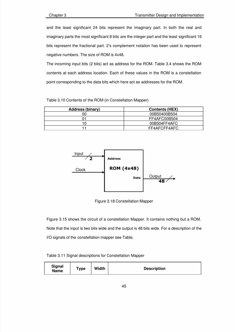
negative numbers. The size of ROM is 4x48.
The incoming input bits (2 bits) act as address for the ROM. Table 3.4 shows the ROM
contents at each address location. Each of these values in the ROM is a constellation
point corresponding to the data bits which here act as addresses for the ROM.
Table 3.10 Contents of the ROM (in Constellation Mapper)
Address (binary) Contents (HEX)00 00B50400B50401 FF4AFC00B50410 00B504FF4AFC11 FF4AFCFF4AFC
Figure 3.18 Constellation Mapper
Figure 3.15 shows the circuit of a constellation Mapper. It contains nothing but a ROM.
Note that the input is two bits wide and the output is 48 bits wide. For a description of the
I/O signals of the constellation mapper see Table.
Table 3.11 Signal descriptions for Constellation Mapper
SignalName
Type Width Description
% 6//78
Input
#
Output
/7
Clock

7/21/2019 FYP Final Report-libre
http://slidepdf.com/reader/full/fyp-final-report-libre 56/109
Chapter 3 Transmitter Design and Implementation
46
in Input 2Input to the constellation mapper (acting as
address for the above shown ROM)
clock Input 1 Positive edge clock
out Output 48Output of the constellation mapper (representing
48 bit complex number)
3.10 INVERSE FAST FOURIER TRANSFORM
In 1971 Discrete Fourier Transform (DFT) was used in baseband
modulation/demodulation in order to achieve orthogonality [24]. Since DFT has heavy
computational requirements, therefore, Fast Fourier Transform (FFT) was utilized. For
an N point discrete Fourier Transform the required number of computations is N(N-1),
but that for FFT/IFFT is Nlog (N), which is much lesser than DFT.
The FFT/IFFT operates on finite sequences. Waveforms which are analog in nature
must be sampled at discrete points before the FFT/IFFT algorithm can be applied.
The Discrete Fourier Transform (DFT) operates on sample time domain signal which is
periodic. The equation for DFT is:
−
=
−
=
1
0
/ 2)()(
N
n
N k jen xk X π 3.11
X(k) represents the DFT frequency output at the k-the spectral point where k ranges
from 0 to N-1. The quantity N represents the number of sample points in the DFT data
frame. The quantity x(n) represents the nth time sample, where n also ranges from 0 to
N-1. In general equation, x(n) can be real or complex.
The corresponding inverse discrete Fourier transform (IDFT) of the sequence X(k) gives
a sequence x(n) defined only on the interval from 0 to N-1 as follows:

7/21/2019 FYP Final Report-libre
http://slidepdf.com/reader/full/fyp-final-report-libre 57/109
Chapter 3 Transmitter Design and Implementation
47
−
=
=
1
0
/ 2)(
1)(
N
k
N k jek X N
n x π
3.12
The DFT equation can be re-written into:
−
=
=
1
0
)()( N
n
nk
N W n xk X 3.13
The quantitynk
N W can be defined as:
N k jnk
N eW / 2π −
= 3.14
This quantity is called Twiddle Factor. It is the sine and cosine basis function written in
polar form [13].
Examination of the first equation reveals that the computation of each point of DFT
requires the following: (N-1) complex multiplication, (N-1) complex addition (first term in
sum involves e j0
= 1). Thus, to compute N points in DFT require N(N-1) complex
multiplication and N(N-1) complex addition.
As N increases, the number of multiplications and additions required is significant
because the multiplication function requires a relatively large amount of processing time
even using computer. Thus, many methods for reducing the number of multiplications
have been investigated over the last 50 years [12].
3.10.1 RADIX-22 ALGORITHM
When the number of data points N in the FFT/IFFT is a power of 4 (i.e., N = 4v), we can,
of course, always use a radix-2 algorithm for the computation. However, for this case, it
is more efficient computationally to employ a radix-r FFT algorithm.

7/21/2019 FYP Final Report-libre
http://slidepdf.com/reader/full/fyp-final-report-libre 58/109
Chapter 3 Transmitter Design and Implementation
48
In the decimation-in-frequency algorithm, the outputs or the frequency domain points are
regrouped or subdivided. Consider the FFT equation:
N k j N
k
en x N
k X
/ 21
0
)(1)(
π −−
== 3.15
As an example we consider N=16. We split or decimate the N -point input sequence into
four subsequences, x(4 n ), x(4 n+1), x(4 n+2), x(4 n+3), n = 0, 1, ... , N /4-1. Therefore, we
get X(k), X(k+N/4), X(k+N/2) and X(k+3N/4). This process is called decimation in
frequency. This decimation continues until each DFT becomes a 4 point DFT. Each 4
point DFT is known as a butterfly when we represent it graphically. Figure 3.16 shows a
radix-4 FFT butterfly.
Since in the proposed design there are 64 sub-carriers so the input to FFT would be 64
complex numbers, hence a 64 point FFT would be required.
For a 4n point FFT n stages are required and N/4 4 point DFTs per stage. Therefore in
our case there would be 3 stages (64 = 43) and 16 4 point DFTs per stage or we can say
16 butterflies pre stage.
Figure 3.19 Radix-4 FFT butterfly
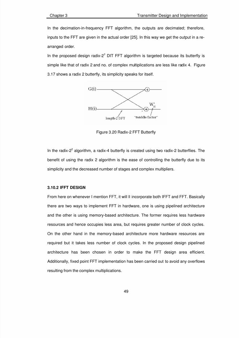
7/21/2019 FYP Final Report-libre
http://slidepdf.com/reader/full/fyp-final-report-libre 59/109
Chapter 3 Transmitter Design and Implementation
49
In the decimation-in-frequency FFT algorithm, the outputs are decimated; therefore,
inputs to the FFT are given in the actual order [25]. In this way we get the output in a re-
arranged order.
In the proposed design radix-22 DIT FFT algorithm is targeted because its butterfly is
simple like that of radix 2 and no. of complex multiplications are less like radix 4. Figure
3.17 shows a radix 2 butterfly, its simplicity speaks for itself.
Figure 3.20 Radix-2 FFT Butterfly
In the radix-22 algorithm, a radix-4 butterfly is created using two radix-2 butterflies. The
benefit of using the radix 2 algorithm is the ease of controlling the butterfly due to its
simplicity and the decreased number of stages and complex multipliers.
3.10.2 IFFT DESIGN
From here on whenever I mention FFT, it will ll incorporate both IFFT and FFT. Basically
there are two ways to implement FFT in hardware, one is using pipelined architecture
and the other is using memory-based architecture. The former requires less hardware
resources and hence occupies less area, but requires greater number of clock cycles.
On the other hand in the memory-based architecture more hardware resources are
required but it takes less number of clock cycles. In the proposed design pipelined
architecture has been chosen in order to make the FFT design area efficient.
Additionally, fixed point FFT implementation has been carried out to avoid any overflows
resulting from the complex multiplications.

7/21/2019 FYP Final Report-libre
http://slidepdf.com/reader/full/fyp-final-report-libre 60/109
Chapter 3 Transmitter Design and Implementation
50
Figure 3.18 shows the I/O diagram of IFFT and description of the I/O parameters is
given in Table 3.7.
Figure 3.21 IFFT I/O diagram
Table 3.12 Signal descriptions for IFFT
SignalName
Type Width Description
arst_n Input 1 Asynchronous reset (negative edged)
clock Input 1 Positive edged clock
enable Input 1When high data is present on the realinput and
imginput lines
realinput Input 24 Real part of the input complex numberImginput Input 24 Imaginary part of the input complex number
Realoutput Output 24 Real part of the output complex number
Imgoutput Output 24 Imaginary part of the output complex number
Complex data is fed in one data-point per clock cycle. The enable signal is asserted the
clock cycle previous to presenting the first data-point.
Figure A.2 is a block diagram of a 64-point Radix-22 fixed-point FFT example. The
module consists of six radix-2 butterflies, shift registers associated with each butterfly,
two complex multipliers, two twiddle factor generators, and a controller that provides the
control signals. The feedback shift registers vary in length from 1 to 32-bits, and are
labeled accordingly.
IFFTrealoutput
clock
arst_n
enableimgoutput
realinput
imginput

7/21/2019 FYP Final Report-libre
http://slidepdf.com/reader/full/fyp-final-report-libre 61/109
Chapter 3 Transmitter Design and Implementation
51
Figure 3.22 Architecture of 64-point-22 FFT
Figure 3.23 bf2i and bf2ii radix 2 butterflies
Each group of two butterflies, consisting of a bf2i and a bf2ii, together emulate a radix-4
butterfly. Figure 3.19 shows the internals of each and how they are connected together.
These modules operate on a principal known as Single-path Delay Feedback (SDF)
[25]. The FFT Radix-2 butterfly must have two inputs in order to produce the next FFT
intermediate value, but the data in our scenario is available only in a serial mode. The
bf2i bf2ii bf2i bf2ii bf2i bf2ii X X
Twiddle Factor Generator
Controller
freg32 freg16 freg8 freg4 freg2 freg1

7/21/2019 FYP Final Report-libre
http://slidepdf.com/reader/full/fyp-final-report-libre 62/109
Chapter 3 Transmitter Design and Implementation
52
SDF mechanism provides a solution where the first input is delayed until the second
input is presented, after which the calculation can proceed. Both the bf2i and bf2ii
modules accomplish this by multiplexing the first input to a shift register of sufficient
length so that that data-point is present at the butterfly input when the second data-point
appears. A counter provides the control signals for these multiplexers, which are internal
to the butterfly modules.
The counter additionally provides signals to the bf2ii for switching the adder operations,
and swapping the real and complex input wires. These mechanisms effect a
multiplication of the input by j.
In order to avoid overflow, the data set is scaled down as it propagates through the
pipeline. The FFT operation consists of a long series of summations, and thus either the
dynamic range of the numerical presentation must be large (floating-point of block
floating-point), or the numerical data must be scaled down. Since the module is fixed
point, the latter strategy is used.
3.11 CYCLIC PREFIX ADDER
Cyclic prefix is basically a replica of a fractional portion of the end of an OFDM symbol
that is placed at the beginning of the symbol. It completely removes inter-symbol
interference that can occur due to Multipath. Cyclic prefix is effective only if its duration
is greater than the delay spread.
3.11.1 DESIGN OF CYCLIC PREFIX ADDER
The architecture of cyclic prefix adder simply consists of an address ROM that stores
addresses, a RAM to store incoming data in sequential order and a counter that
provides read addresses to the RAM. Figure 3.20 shows the top-level architecture of the
cyclic prefix adder. Refer to Table 3.7 for the description of I/O signals.

7/21/2019 FYP Final Report-libre
http://slidepdf.com/reader/full/fyp-final-report-libre 63/109
Chapter 3 Transmitter Design and Implementation
53
Figure 3.24 Top level architecture of cyclic prefix adder
Table 3.13 Signal descriptions for Constellation Mapper
SignalName
Type Width Description
arst_n Input 1 Asynchronous reset (negative edged)
clock Input 1 Positive edged clock
enable Input 1
When high data is present on the realinput and
imginput lines
In Input 48 Input complex number
Out Output 48 Output complex number
In the proposed design, the last eight symbols (complex numbers) of the OFDM symbol
are replicated at the beginning of the symbol, therefore a total of 72 (64 + 8) symbols are
actually transmitted.
Cyclic Prefix Adder
RAM Address ROM
Address counter
in
clock
arst_n
enable
out
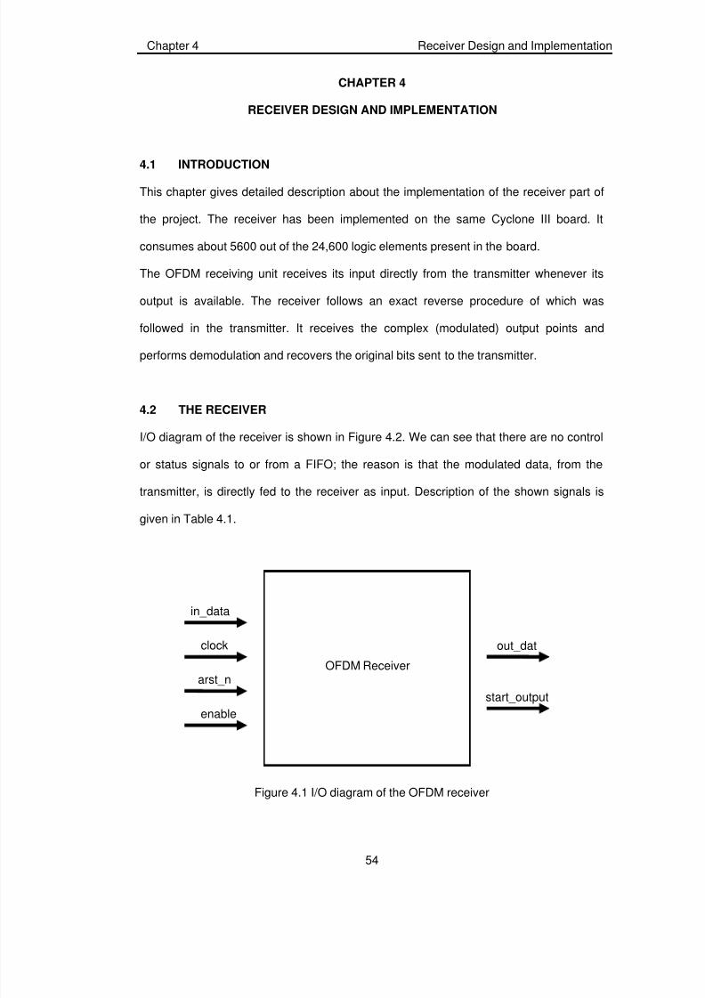
7/21/2019 FYP Final Report-libre
http://slidepdf.com/reader/full/fyp-final-report-libre 64/109
Chapter 4 Receiver Design and Implementation
54
CHAPTER 4
RECEIVER DESIGN AND IMPLEMENTATION
4.1 INTRODUCTION
This chapter gives detailed description about the implementation of the receiver part of
the project. The receiver has been implemented on the same Cyclone III board. It
consumes about 5600 out of the 24,600 logic elements present in the board.
The OFDM receiving unit receives its input directly from the transmitter whenever its
output is available. The receiver follows an exact reverse procedure of which was
followed in the transmitter. It receives the complex (modulated) output points and
performs demodulation and recovers the original bits sent to the transmitter.
4.2 THE RECEIVER
I/O diagram of the receiver is shown in Figure 4.2. We can see that there are no control
or status signals to or from a FIFO; the reason is that the modulated data, from the
transmitter, is directly fed to the receiver as input. Description of the shown signals is
given in Table 4.1.
Figure 4.1 I/O diagram of the OFDM receiver
OFDM Receiver
out_dat
in_data
enable
arst_n
clock
start_output
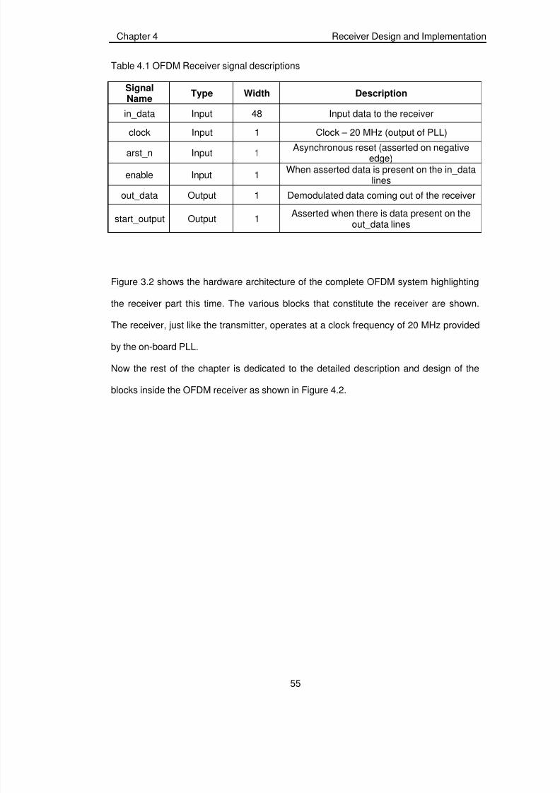
7/21/2019 FYP Final Report-libre
http://slidepdf.com/reader/full/fyp-final-report-libre 65/109
Chapter 4 Receiver Design and Implementation
55
Table 4.1 OFDM Receiver signal descriptions
SignalName
Type Width Description
in_data Input 48 Input data to the receiver
clock Input 1 Clock – 20 MHz (output of PLL)
arst_n Input 1Asynchronous reset (asserted on negative
edge)
enable Input 1When asserted data is present on the in_data
lines
out_data Output 1 Demodulated data coming out of the receiver
start_output Output 1Asserted when there is data present on the
out_data lines
Figure 3.2 shows the hardware architecture of the complete OFDM system highlighting
the receiver part this time. The various blocks that constitute the receiver are shown.
The receiver, just like the transmitter, operates at a clock frequency of 20 MHz provided
by the on-board PLL.
Now the rest of the chapter is dedicated to the detailed description and design of the
blocks inside the OFDM receiver as shown in Figure 4.2.

7/21/2019 FYP Final Report-libre
http://slidepdf.com/reader/full/fyp-final-report-libre 66/109
Chapter 4 Receiver Design and Implementation
56
Figure 4.2 Complete Architecture of the proposed OFDM system (receiver highlighted)
4.3 CYCLIC PREFIX REMOVER
The cyclic prefix was added at the transmitting end in order to avoid inter-symbol
interference, therefore during reception it must be eliminated for any further processing
of the received signal. This is done by simply skipping the first eight sub-carriers in the
O F D M R
e c e i v e r
HSMC TO
SANTA CRUZ
CONNECTOR
RS232Receiver
FIFO
Cyclic prefix remover
FFT
Constellation demapper
Interleaver
Viterbi decoder
RS decoder
Descrambler
RS232 Transmitter
H i g h S p e e d M e z z a n i n
e C o n n e c t o r
I n t e r f a c e
R S 2 3 2
p o r t
On board 50 MHz clock
PLL
Input
C o n t r o l U n i t
FIFO
OFDMTransmitter
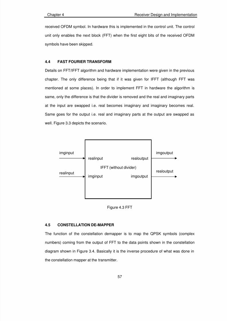
7/21/2019 FYP Final Report-libre
http://slidepdf.com/reader/full/fyp-final-report-libre 67/109
Chapter 4 Receiver Design and Implementation
57
received OFDM symbol. In hardware this is implemented in the control unit. The control
unit only enables the next block (FFT) when the first eight bits of the received OFDM
symbols have been skipped.
4.4 FAST FOURIER TRANSFORM
Details on FFT/IFFT algorithm and hardware implementation were given in the previous
chapter. The only difference being that if it was given for IFFT (although FFT was
mentioned at some places). In order to implement FFT in hardware the algorithm is
same, only the difference is that the divider is removed and the real and imaginary parts
at the input are swapped i.e. real becomes imaginary and imaginary becomes real.
Same goes for the output i.e. real and imaginary parts at the output are swapped as
well. Figure 3.3 depicts the scenario.
Figure 4.3 FFT
4.5 CONSTELLATION DE-MAPPER
The function of the constellation demapper is to map the QPSK symbols (complex
numbers) coming from the output of FFT to the data points shown in the constellation
diagram shown in Figure 3.4. Basically it is the inverse procedure of what was done in
the constellation mapper at the transmitter.
realinput realoutput
IFFT (without divider)
imginput imgoutput
imginput
realinput
imgoutput
realoutput

7/21/2019 FYP Final Report-libre
http://slidepdf.com/reader/full/fyp-final-report-libre 68/109
Chapter 4 Receiver Design and Implementation
58
Figure 4.4 QPSK constellation diagram
4.5.1 DESIGN OF CONSTELLATION DE-MAPPER
The mapping of data points to QPSK symbols (as done in the transmitter) is shown in
Table 4.3.
Table 4.2 Data points mapped to constellation points
Address (binary) Constellation points Constellation points (HEX)00 0.707 + j0.707 00B50400B50401 -0.707 + j0.707 FF4AFC00B50410 0.707 – j0.707 00B504FF4AFC11 -0.707 – j0.707 FF4AFCFF4AFC
Therefore, basically the incoming constellation points are mapped onto the data points
as shown in Table 3.4. Figure 4.5 shows the I/O diagram of the constellation demapper
and Table 3.5 shows the description of the signals.
Figure 4.5 I/O diagram of constellation demapper
ConstellationDemapper
clock
arst_n
in
out

7/21/2019 FYP Final Report-libre
http://slidepdf.com/reader/full/fyp-final-report-libre 69/109
Chapter 4 Receiver Design and Implementation
59
Table 4.3 Signal descriptions for Constellation De-mapper
SignalName
Type Width Description
in Input 48 Input constellation points
clock Input 1 Positive edge clock
out Output 2 Output data points corresponding to Table 4.3
arst_n Input 1 Asynchronous reset (Negative edged)
Instead of going into the hardware architecture, the design is shown using the Verilog
code. A simple switch-case structure is used to construct the design. The code is shown
below:
Figure 4.6 Verilog code showing the logic behind implementation of constellation
demapper
4.6 DE-INTERLEAVER
In the previous chapter interleaving was defined as a process in which bits, within a
block of 128 bits, are re-arranged in order to avoid burst errors. De-interleaving performs
the inverse task. It re-arranges the interleaved bits into their original order.
Recall the row-column method of interleaving discussed in the previous chapter. De-
interleaving is done the same way, the difference being that the number of rows and the
number of columns for de-interleaving are interchanged. For example if we perform
always @(in)begin
case ({in[47], in[23]})2'b00: tmp_out = 2'b00;2'b01: tmp_out = 2'b10;2'b10: tmp_out = 2'b01;2'b11: tmp_out = 2'b11;default: tmp_out = 2'b00;
endcaseend
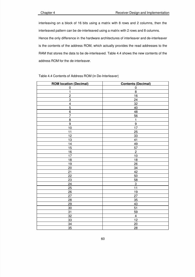
7/21/2019 FYP Final Report-libre
http://slidepdf.com/reader/full/fyp-final-report-libre 70/109
Chapter 4 Receiver Design and Implementation
60
interleaving on a block of 16 bits using a matrix with 8 rows and 2 columns, then the
interleaved pattern can be de-interleaved using a matrix with 2 rows and 8 columns.
Hence the only difference in the hardware architectures of interleaver and de-interleaver
is the contents of the address ROM, which actually provides the read addresses to the
RAM that stores the data to be de-interleaved. Table 4.4 shows the new contents of the
address ROM for the de-interleaver.
Table 4.4 Contents of Address ROM (in De-Interleaver)
ROM location (Decimal) Contents (Decimal)
0 0
1 8
2 163 24
4 32
5 40
6 48
7 56
8 1
9 9
10 17
11 2512 33
13 41
14 4915 57
16 2
17 10
18 18
19 26
20 34
21 4222 50
23 58
24 325 11
26 19
27 27
28 35
29 43
30 5131 59
32 4
33 1234 20
35 28

7/21/2019 FYP Final Report-libre
http://slidepdf.com/reader/full/fyp-final-report-libre 71/109
Chapter 4 Receiver Design and Implementation
61
36 3637 44
38 52
39 60
40 5
41 13
42 2143 29
44 37
45 4546 53
47 61
48 649 14
50 22
51 30
52 38
53 46
54 5455 6256 7
57 15
58 2359 31
60 39
61 47
62 55
63 63
4.7 VITERBI DECODER
The Viterbi Decoder decodes Convolutional codes. We have used the Altera’s Viterbi
Decoder IP core in our design. Altera’s Viterbi IP core is a parameterized IP core that is
synthesizable and allows for parallel as well as hybrid implementation of the Viterbi
decoder.
4.8 REED SOLOMON DECODER
The Reed Solomon decoder decodes the codes generated by the Reed Solomon
Encoder. For the implementation of the Reed Solomon Decoder we have again used
Altera’s Reed Solomon Decoder IP.
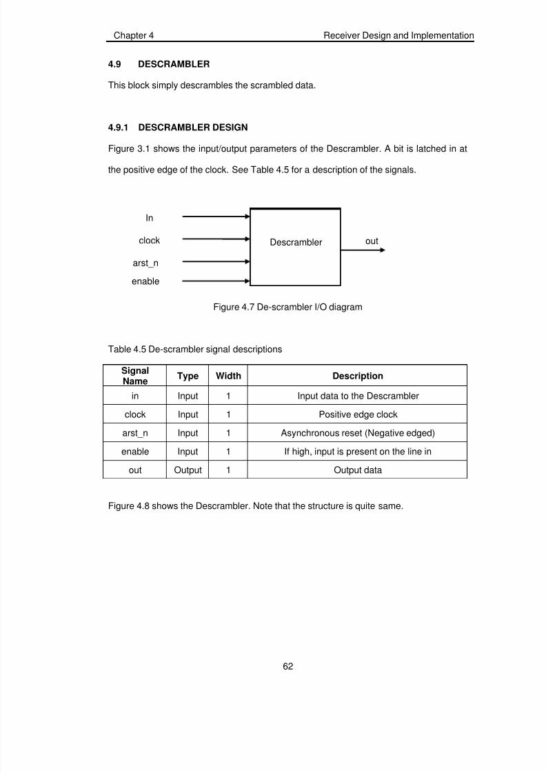
7/21/2019 FYP Final Report-libre
http://slidepdf.com/reader/full/fyp-final-report-libre 72/109
Chapter 4 Receiver Design and Implementation
62
4.9 DESCRAMBLER
This block simply descrambles the scrambled data.
4.9.1 DESCRAMBLER DESIGN
Figure 3.1 shows the input/output parameters of the Descrambler. A bit is latched in at
the positive edge of the clock. See Table 4.5 for a description of the signals.
Figure 4.7 De-scrambler I/O diagram
Table 4.5 De-scrambler signal descriptions
SignalName
Type Width Description
in Input 1 Input data to the Descrambler
clock Input 1 Positive edge clock
arst_n Input 1 Asynchronous reset (Negative edged)
enable Input 1 If high, input is present on the line in
out Output 1 Output data
Figure 4.8 shows the Descrambler. Note that the structure is quite same.
Descrambler out
In
clock
arst_n
enable

7/21/2019 FYP Final Report-libre
http://slidepdf.com/reader/full/fyp-final-report-libre 73/109
Chapter 4 Receiver Design and Implementation
63
Figure 4.8 De-scrambler logic diagram
6 5 4 3 2 1 0
,,
out
in
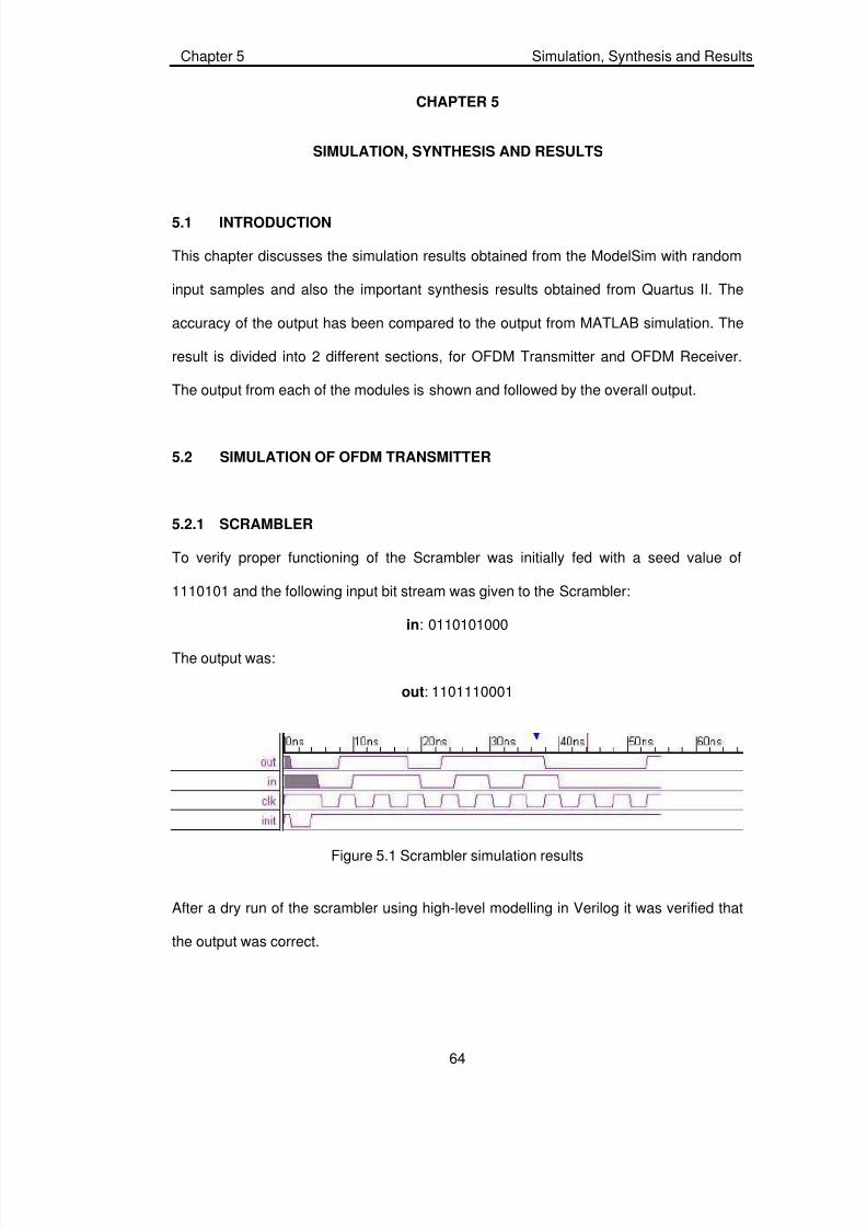
7/21/2019 FYP Final Report-libre
http://slidepdf.com/reader/full/fyp-final-report-libre 74/109
Chapter 5 Simulation, Synthesis and Results
64
CHAPTER 5
SIMULATION, SYNTHESIS AND RESULTS
5.1 INTRODUCTION
This chapter discusses the simulation results obtained from the ModelSim with random
input samples and also the important synthesis results obtained from Quartus II. The
accuracy of the output has been compared to the output from MATLAB simulation. The
result is divided into 2 different sections, for OFDM Transmitter and OFDM Receiver.
The output from each of the modules is shown and followed by the overall output.
5.2 SIMULATION OF OFDM TRANSMITTER
5.2.1 SCRAMBLER
To verify proper functioning of the Scrambler was initially fed with a seed value of
1110101 and the following input bit stream was given to the Scrambler:
in: 0110101000
The output was:
out: 1101110001
Figure 5.1 Scrambler simulation results
After a dry run of the scrambler using high-level modelling in Verilog it was verified that
the output was correct.
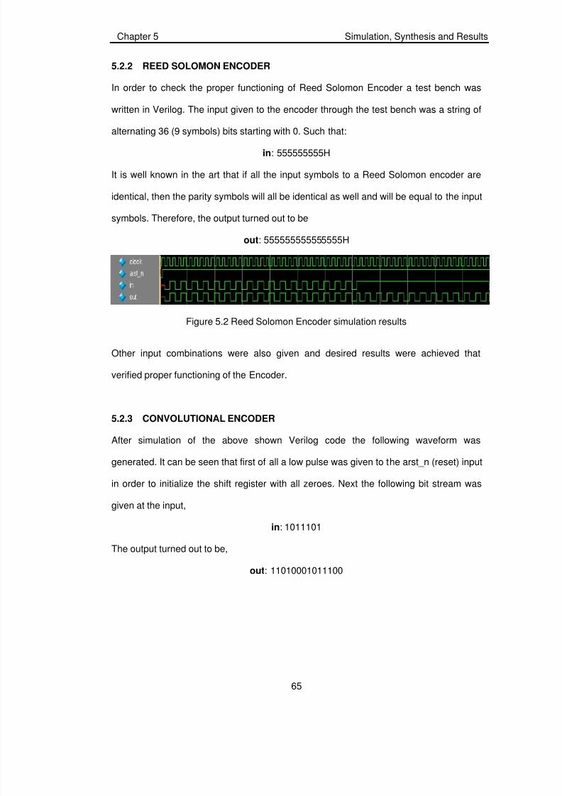
7/21/2019 FYP Final Report-libre
http://slidepdf.com/reader/full/fyp-final-report-libre 75/109
Chapter 5 Simulation, Synthesis and Results
65
5.2.2 REED SOLOMON ENCODER
In order to check the proper functioning of Reed Solomon Encoder a test bench was
written in Verilog. The input given to the encoder through the test bench was a string of
alternating 36 (9 symbols) bits starting with 0. Such that:
in: 555555555H
It is well known in the art that if all the input symbols to a Reed Solomon encoder are
identical, then the parity symbols will all be identical as well and will be equal to the input
symbols. Therefore, the output turned out to be
out: 555555555555555H
Figure 5.2 Reed Solomon Encoder simulation results
Other input combinations were also given and desired results were achieved that
verified proper functioning of the Encoder.
5.2.3 CONVOLUTIONAL ENCODER
After simulation of the above shown Verilog code the following waveform was
generated. It can be seen that first of all a low pulse was given to the arst_n (reset) input
in order to initialize the shift register with all zeroes. Next the following bit stream was
given at the input,
in: 1011101
The output turned out to be,
out: 11010001011100
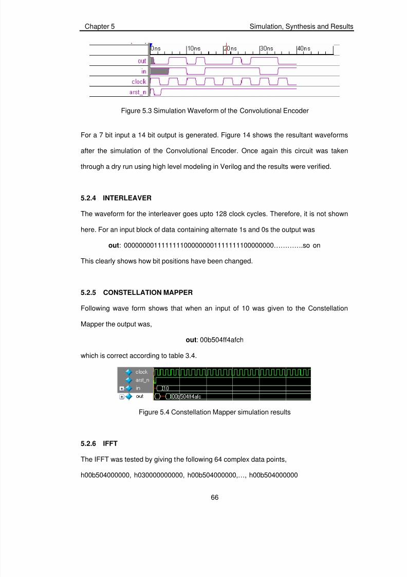
7/21/2019 FYP Final Report-libre
http://slidepdf.com/reader/full/fyp-final-report-libre 76/109
Chapter 5 Simulation, Synthesis and Results
66
Figure 5.3 Simulation Waveform of the Convolutional Encoder
For a 7 bit input a 14 bit output is generated. Figure 14 shows the resultant waveforms
after the simulation of the Convolutional Encoder. Once again this circuit was taken
through a dry run using high level modeling in Verilog and the results were verified.
5.2.4 INTERLEAVER
The waveform for the interleaver goes upto 128 clock cycles. Therefore, it is not shown
here. For an input block of data containing alternate 1s and 0s the output was
out: 0000000011111111000000001111111100000000………….so on
This clearly shows how bit positions have been changed.
5.2.5 CONSTELLATION MAPPER
Following wave form shows that when an input of 10 was given to the Constellation
Mapper the output was,
out: 00b504ff4afch
which is correct according to table 3.4.
Figure 5.4 Constellation Mapper simulation results
5.2.6 IFFT
The IFFT was tested by giving the following 64 complex data points,
h00b504000000, h030000000000, h00b504000000,…, h00b504000000

7/21/2019 FYP Final Report-libre
http://slidepdf.com/reader/full/fyp-final-report-libre 77/109
Chapter 5 Simulation, Synthesis and Results
67
which is equivalent to 0.707, 3, 0.707,…, 0.707
Figure 5.5 IFFT simulation results
The outputs were,
h2f8bc000000, h5db504000000, h0000005db504 and so on. On verification with
MATLAB the results turned out to be correct.
5.2.7 CYCLIC PREFIX ADDER
The inputs given to the cyclic prefix adder were
47'h000000100101, 47'h000010100001, 47'h001110100101, 47'h110010100101,
47'h000010100101, 47'h010101000101, 47'h011110100101, 47'h000011100101. . .
47'h000011100101
The outputs turned out to be
47'h000011100101, 47'h000011100101, 47'h000011100101, 47'h000011100101,
47'h000011100101, 47'h000011100101, 47'h000011100101, 47'h000011100101,
47'h000000100101, 47'h000010100001, 47'h001110100101, 47'h110010100101,
47'h000010100101, 47'h010101000101, 47'h011110100101, 47'h000011100101. . .
47'h000011100101
Note that the first eight outputs are actually the last eight inputs and the rest of the
output points are same as the inputs. The following waveform shows the same
Figure 5.6 Cyclic Prefix Adder simulation result

7/21/2019 FYP Final Report-libre
http://slidepdf.com/reader/full/fyp-final-report-libre 78/109
Chapter 5 Simulation, Synthesis and Results
68
5.3 SYNTHESIS OF OFDM TRANSMITTER
Table 5.1 shows some important synthesis results for each module of the OFDM
transmitter.
Table 5.1 Important Synthesis results for the OFDM Transmitter
Module (Entity) Number of logic elements Number of memory bitsScrambler 17 0
Reed Solomon Encoder 49 0Convolutional Encoder 10 0
Interleaver 38 640Constellation Mapper 0 192
IFFT 1992 6336Cyclic Prefix Adder 84 6528
Total 2190 13696
5.4 SIMULATION OF OFDM RECEIVER
The Cyclic Prefix Remover simply removes the cyclic portion added at the transmitting
end, and the simulation of the next block FFT is similar to IFFT so it is not shown. In
addition to these blocks the simulations of Viterbi Decoder and Reed Solomon Decoder
are also not shown because their ip cores are used in the project. Simulation results for
the Constellation De-Mapper, De-Interleaver and De-Scrambler follow.
5.4.1 CONSTELLATION DE-MAPPER
As described in previous chapters, the constellation demapper basically maps the
incoming QPSK constellation points to actual data according to table 3.4.
On the following inputs:
h00b50400b504 (which is 0.707 + j0.707)
and
hFF4AFC00B504 (which is -0.707 + j 0.707)
The outputs turned out to be,
00 and 01
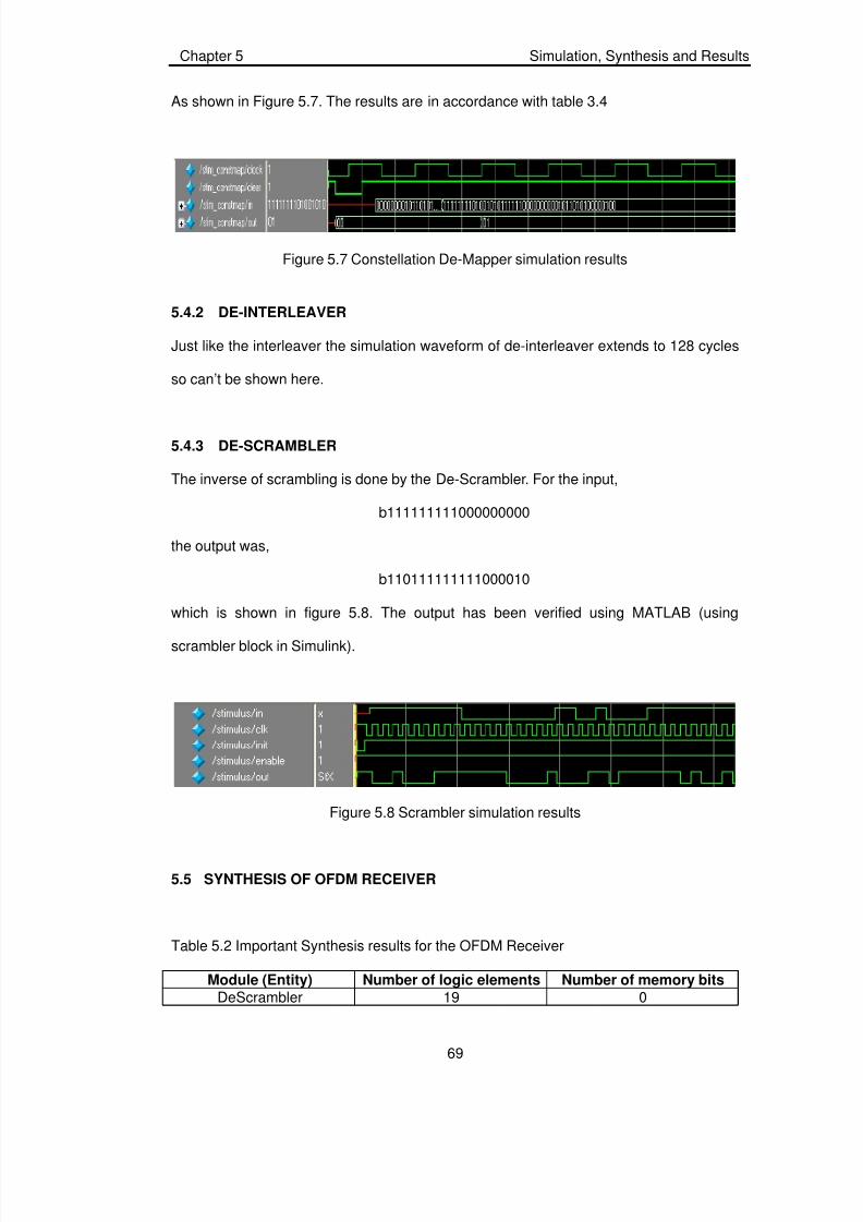
7/21/2019 FYP Final Report-libre
http://slidepdf.com/reader/full/fyp-final-report-libre 79/109
Chapter 5 Simulation, Synthesis and Results
69
As shown in Figure 5.7. The results are in accordance with table 3.4
Figure 5.7 Constellation De-Mapper simulation results
5.4.2 DE-INTERLEAVER
Just like the interleaver the simulation waveform of de-interleaver extends to 128 cycles
so can’t be shown here.
5.4.3 DE-SCRAMBLER
The inverse of scrambling is done by the De-Scrambler. For the input,
b111111111000000000
the output was,
b110111111111000010
which is shown in figure 5.8. The output has been verified using MATLAB (using
scrambler block in Simulink).
Figure 5.8 Scrambler simulation results
5.5 SYNTHESIS OF OFDM RECEIVER
Table 5.2 Important Synthesis results for the OFDM Receiver
Module (Entity) Number of logic elements Number of memory bitsDeScrambler 19 0

7/21/2019 FYP Final Report-libre
http://slidepdf.com/reader/full/fyp-final-report-libre 80/109
Chapter 5 Simulation, Synthesis and Results
70
Reed Solomon Decoder 200 0Viterbi Decoder 900 256De-Interleaver 38 640
Constellation De-Mapper 100 0FFT 1992 6336Total 5439 7232
7/21/2019 FYP Final Report-libre
http://slidepdf.com/reader/full/fyp-final-report-libre 81/109
References
71
REFERENCES
[1] Ahmed R. S. Bahai and Burton R. Saltzberg, Multi Carrier Digital
Communications. Kluwer Academic Publishers, 2002.
[2] “Scrambler (Randomizer)”, Wikipedia the free encyclopediahttp://en.wikipedia.org/wiki/Scrambler_%28randomizer%29.
[3] “Encoding-Decoding Reed Solomon codes”, Adina Matache Department ofElectrical Engineering University of Washingtonhttp://www.ee.ucla.edu/~matache/rsc/node3.html#SECTION000210000000000
00000.
[4] “A Tutorial on Convolutional Coding with Viterbi Decoding”, SpectrumApplicationshttp://home.netcom.com/~chip.f/viterbi/tutorial.html.
[5] “Interleaver”, Wikipedia the free encyclopediahttp://en.wikipedia.org/wiki/Interleaver.
[6] Jeffrey G. Andrews, Rias Muhammad, Fundamentals of WIMAX . Prentice HallCommunications Engineering, 2006.
[7] Aseem Pandey, Shyam Ratan Agrawalla & Shrikant Manivannan, “VLSIImplementation of OFDM”, Wipro Technologies, September 2002.
[8] Dusan Matiae, “OFDM as a possible modulation technique for multimediaapplications in the range of mm waves”, TUD-TVS, 1998.
[9] J. L. Holsinger, “Digital communication over fixed time-continuous channelswith memory, with special application to telephone channels,” PhD thesis,Massachusetts Institute of Technology, 1964.
[10] R. W. Chang, “Synthesis of band-limited orthogonal signals for multichanneldata transmission,” Bell Systems Technical Journal, 45:1775–1796, December1966.
[11] R. G. Gallager, Information Theory and Reliable Communications. Wiley, 1968.
[12] S. Weinstein and P. Ebert “Data transmission by frequency-division multiplexingusing the discrete Fourier transform.” IEEE Transactions on Communications,
19(5):628–634, October 1971.
[13] L. J. Cimini “Analysis and simulation of a digital mobile channel usingorthogonal frequency division multiplexing.” IEEE Transactions on
Communications, 33(7):665–675, July 1985.
[14] Lattice Semiconductor white paper, “Implementing WiMAX OFDM Timing andFrequency Offset Estimation in Lattice FPGAs,” 2005.

7/21/2019 FYP Final Report-libre
http://slidepdf.com/reader/full/fyp-final-report-libre 82/109
References
72
[15] Doelz, M.L., Heald E.T. and Martin D.L. "Binary Data Transmission Techniquesfor Linear Systems." Proc. I.R.E., 45: 656-661, May 1957.
[16] S. B. Weinstein and P. M. Ebert, “Data transmission by frequency-divisionmultiplexing using the discrete Fourier transform”, IEEE Trans. Communications,COM-19(5): 628-634, Oct. 1971.
[17] “Orthogonal Frequency Division Multiplexing Tutorial”, Intuitive guide toPrinciples of Communicationshttp://www.complextoreal.com
[18] Magis Networks White paper, “Orthogonal Frequency Division Multiplexing(OFDM) Explained,” Inc. 2001
[19] “Orthogonal Frequency-Division Multiplexing (OFDM)”, the International Unionof Radio Science (URSI), Lulea University of Technology, 2002
[20] Michael D. Ciletti, Advanced Digital Design with the Verilog HD Xilinx Design Series. Prentice Hall, 2002.
[21] “Reed Solomon error-correction code”, Wikipedia the free Encyclopediahttp://en.wikipedia.org/wiki/Reed-Solomon_error_correction
[22] Bernard Sklar. Digital Communications- Fundamentals and Applications.Communication Engineering Services, Tarzana, California, 2003
[23] “Interleaver”, Wikipedia the free encyclopediahttp://en.wikipedia.org/wiki/Interleaver
[24] “DFT”, Wikipedia the free Encyclopediaen.wikipedia.org/wiki/Discrete_Fourier_transform
[25] “Fast Fourier Transform”, Molfram MathWorld mathworld.wolfram.com/FastFourierTransform.html
7/21/2019 FYP Final Report-libre
http://slidepdf.com/reader/full/fyp-final-report-libre 83/109
Appendix A RTL code in Verilog for OFDM Transmitter
73
APPENDIX A
RTL CODE IN VERILOG FOR OFDM TRANSMITTER
//**********************************************
// OFDM System - OFDM Transmitter and
// Receiver
//**********************************************
module OFDMSystem (
input in,
input clock,
input arst_n,
output TxD,
output start_output
);
wire clock1, clock2;
wire out_fifo, readreq;
wire wrempty;
wire readfull, readempty;
wire [7:0] in_data;
wire wrfull;
wire [7:0] q;
wire [47:0] out_data;
wire idle, RxD_data_ready;
wire rdempty1, rdfull1, wrempty1, wrfull1;wire [9:0] rdusedw;
wire [6:0] wrusedw;
wire TxD_busy, startserialtrans;
reg start_serialtrans, start_trans;
reg [2:0] skipbytecount;
//******************************************
//PLL
//******************************************
PLL pll(
clock,
clock1,
clock2
);
//*****************************************
//FIFO
//*****************************************
7/21/2019 FYP Final Report-libre
http://slidepdf.com/reader/full/fyp-final-report-libre 84/109
Appendix A RTL code in Verilog for OFDM Transmitter
74
fifo input_data_fifo (
in_data,
clock1,
readreq,
clock2,
RxD_data_ready,
out_fifo,
readempty,
readfull,
wrempty,
wrfull
);
//***************************************
// OFDM Transmitter module
//***************************************
OFDM_transmitter transmitter (
clock1,
arst_n,
out_fifo,out_data,
wrfull,
readreq,
readempty,
start_output
);
//****************************************
// RS-232 Asyncronous Receiver
//****************************************
async_receiver SerialReceiver(
clock2,
arst_n,
in,
RxD_data_ready,
in_data,
idle
);
//****************************************
// RS-232 Asyncronous Transmitter
//****************************************
async_transmitter serialtrans(
clock2,
arst_n,start_trans,
q,
TxD,
TxD_busy
);
//*******************************************
// FIFO for storing transmitter's output
//*******************************************

7/21/2019 FYP Final Report-libre
http://slidepdf.com/reader/full/fyp-final-report-libre 85/109
Appendix A RTL code in Verilog for OFDM Transmitter
75
trans_out_fifo fifo(
{out_data,16'd0},
clock2,
(start_serialtrans & ~TxD_busy & !start_trans),
clock1,
start_output,
q,
rdempty1,
rdfull1,
rdusedw,
wrempty1,
wrfull1,
wrusedw
);
//*********************************************************
always @(posedge clock2 or negedge arst_n)
begin
if(!arst_n)start_serialtrans <= 1'b0;
else if(wrusedw==71)
start_serialtrans <= 1'b1;
else if(rdempty1)
start_serialtrans <= 1'b0;
end
//*********************************************************
always @(posedge clock2 or negedge arst_n)
begin
if(!arst_n)
start_trans <= 1'b0;
else if(start_serialtrans && !TxD_busy &&
skipbytecount!=0 && skipbytecount!=1)
start_trans <= 1'b1;
else if(TxD_busy)
start_trans <= 1'b0;
end
//*********************************************************
always @(posedge clock2 or negedge arst_n)
begin
if(!arst_n)
skipbytecount <= 3'd0;
else if(start_serialtrans && !TxD_busy && !start_trans)skipbytecount <= skipbytecount + 3'd1;
else if(!start_serialtrans)
skipbytecount <= 3'd0;
end
endmodule
//*****************************************

7/21/2019 FYP Final Report-libre
http://slidepdf.com/reader/full/fyp-final-report-libre 86/109
Appendix A RTL code in Verilog for OFDM Transmitter
76
// OFDM Transmitter top-level module//*****************************************
module OFDM_transmitter (
input clock,
input arst_n,
input in_data,
output [47:0] out_data,
input wrfull,
output readreq,
input readempty,
output start_output
);
//intermediate outputs of the various blocks
wire scrambler_out, rs_out, even_conv, odd_conv;
wire [1:0] interleaver_out;
wire [47:0] constmap_out, ifft_out, cyclic_out;
//The control word
wire [6:0] controlword;
//************************************
//Control Unit
//************************************
ControlUnit controlunit (
clock,
arst_n,
wrfull,
readempty,
readreq,
controlword
);
//*************************************
//Scrambler
//*************************************
Scrambler scrambler (
clock,
arst_n,
controlword[6],
in_data,
scrambler_out
);
//***************************************
//Reed Solomon [RS (15,9)] encoder
//***************************************
ReedSolomon_Encoder rs_enc (
clock,
scrambler_out,
controlword[5],
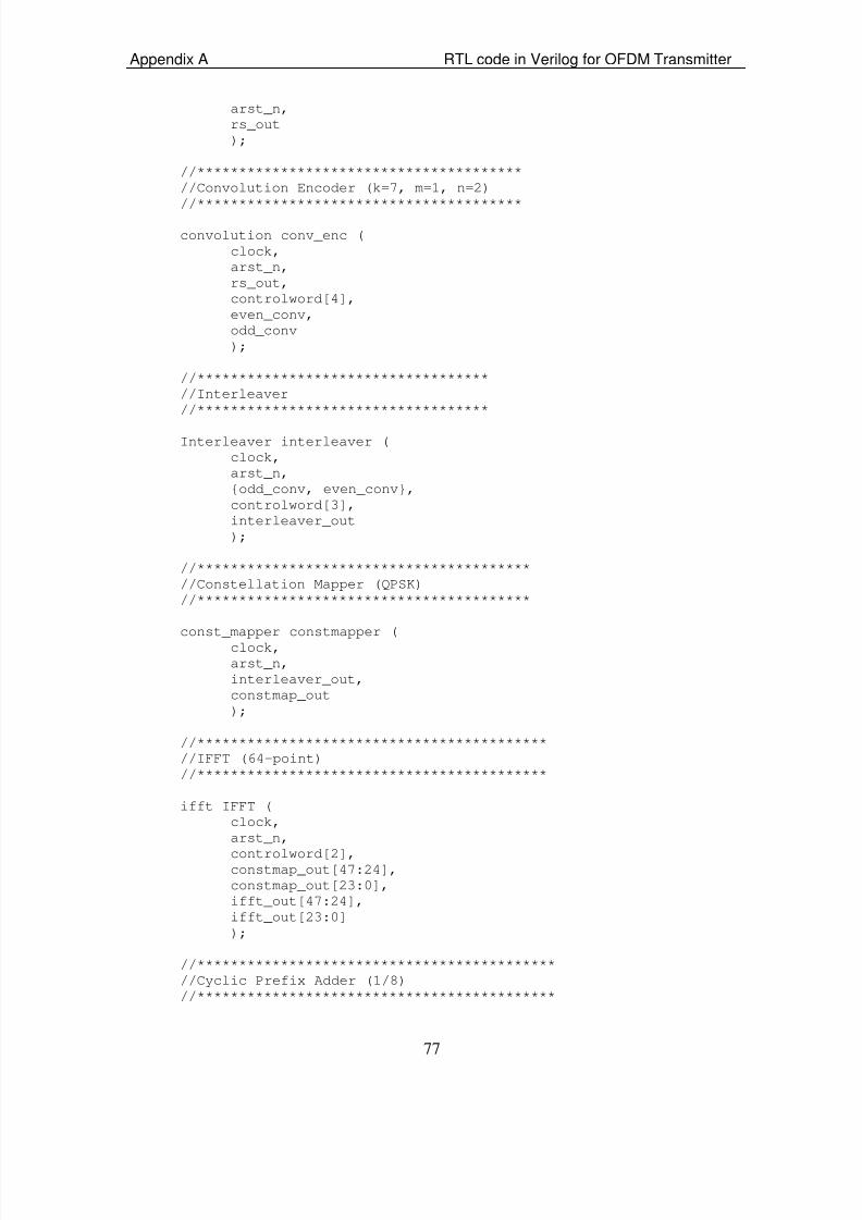
7/21/2019 FYP Final Report-libre
http://slidepdf.com/reader/full/fyp-final-report-libre 87/109
Appendix A RTL code in Verilog for OFDM Transmitter
77
arst_n,
rs_out
);
//***************************************
//Convolution Encoder (k=7, m=1, n=2)
//***************************************
convolution conv_enc (
clock,
arst_n,
rs_out,
controlword[4],
even_conv,
odd_conv
);
//***********************************
//Interleaver
//***********************************
Interleaver interleaver (
clock,
arst_n,
{odd_conv, even_conv},
controlword[3],
interleaver_out
);
//****************************************
//Constellation Mapper (QPSK)
//****************************************
const_mapper constmapper (
clock,
arst_n,
interleaver_out,
constmap_out
);
//******************************************
//IFFT (64-point)
//******************************************
ifft IFFT (
clock,
arst_n,
controlword[2],constmap_out[47:24],
constmap_out[23:0],
ifft_out[47:24],
ifft_out[23:0]
);
//*******************************************
//Cyclic Prefix Adder (1/8)
//*******************************************
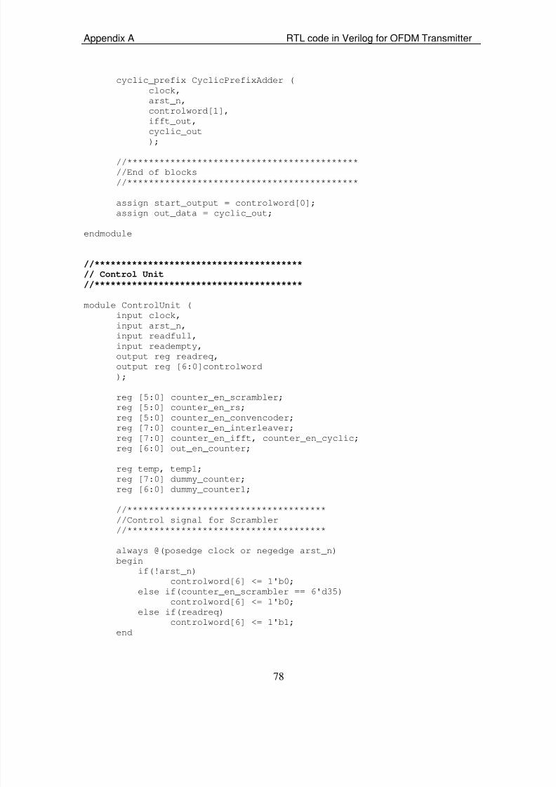
7/21/2019 FYP Final Report-libre
http://slidepdf.com/reader/full/fyp-final-report-libre 88/109
Appendix A RTL code in Verilog for OFDM Transmitter
78
cyclic_prefix CyclicPrefixAdder (
clock,
arst_n,
controlword[1],
ifft_out,
cyclic_out
);
//*******************************************
//End of blocks
//*******************************************
assign start_output = controlword[0];
assign out_data = cyclic_out;
endmodule
//***************************************
// Control Unit//***************************************
module ControlUnit (
input clock,
input arst_n,
input readfull,
input readempty,
output reg readreq,
output reg [6:0]controlword
);
reg [5:0] counter_en_scrambler;
reg [5:0] counter_en_rs;
reg [5:0] counter_en_convencoder;
reg [7:0] counter_en_interleaver;
reg [7:0] counter_en_ifft, counter_en_cyclic;
reg [6:0] out_en_counter;
reg temp, temp1;
reg [7:0] dummy_counter;
reg [6:0] dummy_counter1;
//*************************************
//Control signal for Scrambler
//*************************************
always @(posedge clock or negedge arst_n)begin
if(!arst_n)
controlword[6] <= 1'b0;
else if(counter_en_scrambler == 6'd35)
controlword[6] <= 1'b0;
else if(readreq)
controlword[6] <= 1'b1;
end

7/21/2019 FYP Final Report-libre
http://slidepdf.com/reader/full/fyp-final-report-libre 89/109
Appendix A RTL code in Verilog for OFDM Transmitter
79
always @(posedge clock or negedge arst_n)
begin
if(!arst_n)
counter_en_scrambler <= 6'b000000;
else if(counter_en_scrambler == 6'd35)
counter_en_scrambler <= 6'b000000;
else if(controlword[6])
counter_en_scrambler <= counter_en_scrambler + 6'd1;
end
//****************************************
//Control signal for Reed Solomon Encoder
//****************************************
always @(posedge clock or negedge arst_n)
begin
if(!arst_n)
controlword[5] <= 1'b0;
else if(counter_en_rs == 6'd60)
controlword[5] <= 1'b0;
else if(controlword[6])controlword[5] <= 1'b1;
end
always @(posedge clock or negedge arst_n)
begin
if(!arst_n)
counter_en_rs <= 6'b000000;
else if(counter_en_rs == 6'd60)
counter_en_rs <= 6'b000000;
else if(controlword[5])
counter_en_rs <= counter_en_rs + 6'd1;
end
//*****************************************
//Control signal for convolutional encoder
//*****************************************
always @(posedge clock or negedge arst_n)
begin
if(!arst_n)
controlword[4] <= 1'b0;
else if(counter_en_convencoder == 6'd59)
controlword[4] <= 1'b0;
else if(controlword[5])
controlword[4] <= 1'b1;
end
always @(posedge clock or negedge arst_n)
begin
if(!arst_n)
counter_en_convencoder <= 6'b000000;
else if(counter_en_convencoder == 6'd59)
counter_en_convencoder <= 6'b000000;
else if(controlword[4])
counter_en_convencoder <= counter_en_convencoder +
6'd1;
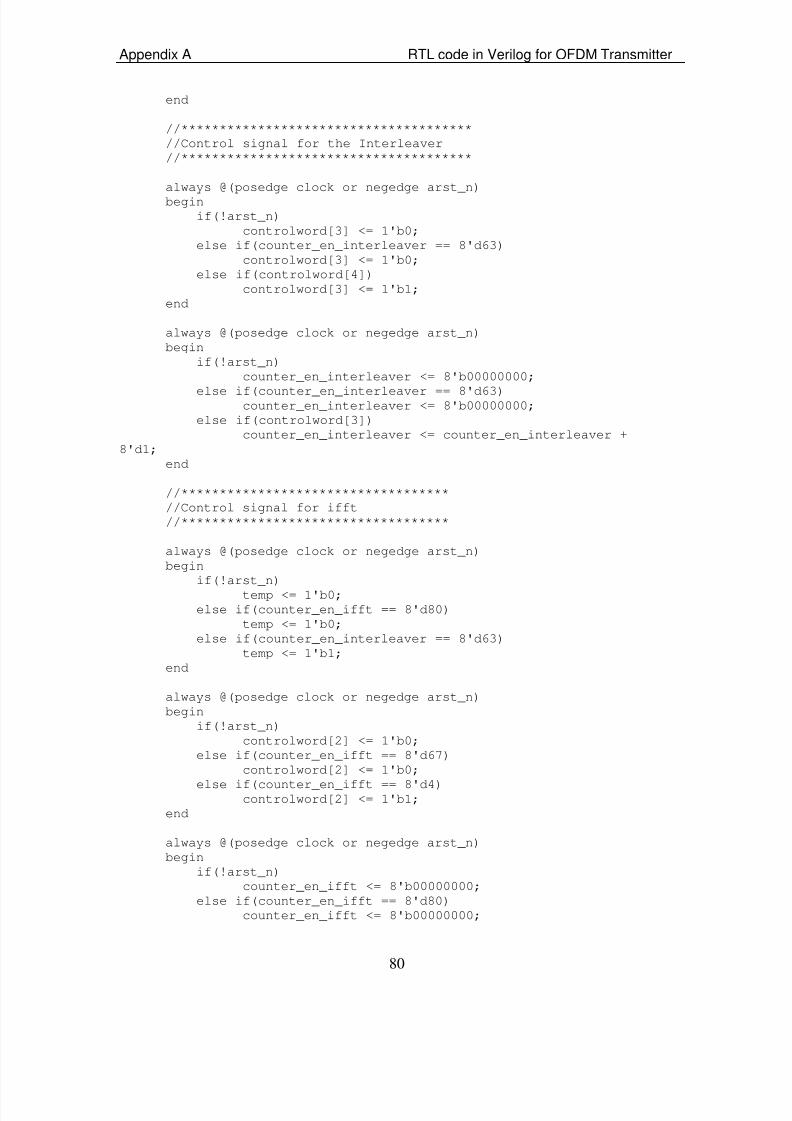
7/21/2019 FYP Final Report-libre
http://slidepdf.com/reader/full/fyp-final-report-libre 90/109
Appendix A RTL code in Verilog for OFDM Transmitter
80
end
//**************************************
//Control signal for the Interleaver
//**************************************
always @(posedge clock or negedge arst_n)
begin
if(!arst_n)
controlword[3] <= 1'b0;
else if(counter_en_interleaver == 8'd63)
controlword[3] <= 1'b0;
else if(controlword[4])
controlword[3] <= 1'b1;
end
always @(posedge clock or negedge arst_n)
begin
if(!arst_n)
counter_en_interleaver <= 8'b00000000;
else if(counter_en_interleaver == 8'd63)counter_en_interleaver <= 8'b00000000;
else if(controlword[3])
counter_en_interleaver <= counter_en_interleaver +
8'd1;
end
//***********************************
//Control signal for ifft
//***********************************
always @(posedge clock or negedge arst_n)
begin
if(!arst_n)
temp <= 1'b0;
else if(counter_en_ifft == 8'd80)
temp <= 1'b0;
else if(counter_en_interleaver == 8'd63)
temp <= 1'b1;
end
always @(posedge clock or negedge arst_n)
begin
if(!arst_n)
controlword[2] <= 1'b0;
else if(counter_en_ifft == 8'd67)
controlword[2] <= 1'b0;
else if(counter_en_ifft == 8'd4)controlword[2] <= 1'b1;
end
always @(posedge clock or negedge arst_n)
begin
if(!arst_n)
counter_en_ifft <= 8'b00000000;
else if(counter_en_ifft == 8'd80)
counter_en_ifft <= 8'b00000000;

7/21/2019 FYP Final Report-libre
http://slidepdf.com/reader/full/fyp-final-report-libre 91/109
Appendix A RTL code in Verilog for OFDM Transmitter
81
else if(temp)
counter_en_ifft <= counter_en_ifft + 8'd1;
end
//***************************************
//Control signal for cyclic prefix
//***************************************
always @(posedge clock or negedge arst_n)
begin
if(!arst_n)
controlword[1] <= 1'b0;
else if(counter_en_ifft == 8'd80)
controlword[1] <= 1'b1;
else if(counter_en_cyclic == 8'd65)
controlword[1] <= 1'b0;
end
always @(posedge clock or negedge arst_n)
begin
if(!arst_n)counter_en_cyclic <= 8'b00000000;
else if(counter_en_cyclic == 8'd65)
counter_en_cyclic <= 8'b00000000;
else if(controlword[1])
counter_en_cyclic <= counter_en_cyclic + 8'd1;
end
//****************************************
//Output control signal
//****************************************
always @(posedge clock or negedge arst_n)
begin
if(!arst_n)
dummy_counter1 <= 7'b0000000;
else if(dummy_counter1 == 7'd66)
dummy_counter1 <= 7'b0000000;
else if(controlword[1])
dummy_counter1 <= dummy_counter1 + 7'd1;
end
always @(posedge clock or negedge arst_n)
begin
if(!arst_n)
controlword[0] <= 1'b0;
else if(dummy_counter1 == 8'd66)
controlword[0] <= 1'b1;else if(out_en_counter == 7'd71)
controlword[0] <= 1'b0;
end
always @(posedge clock or negedge arst_n)
begin
if(!arst_n)
out_en_counter <= 7'b0000000;
else if(out_en_counter == 7'd71)
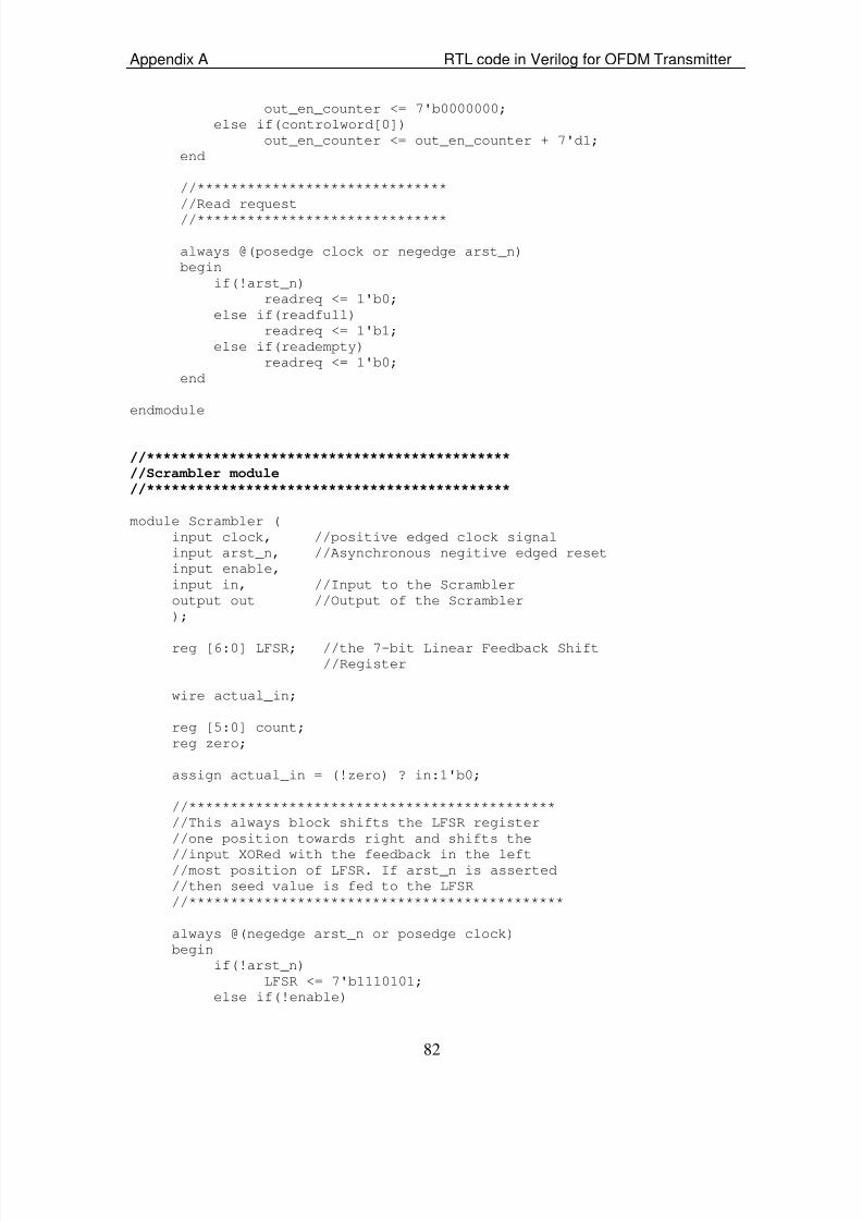
7/21/2019 FYP Final Report-libre
http://slidepdf.com/reader/full/fyp-final-report-libre 92/109
Appendix A RTL code in Verilog for OFDM Transmitter
82
out_en_counter <= 7'b0000000;
else if(controlword[0])
out_en_counter <= out_en_counter + 7'd1;
end
//******************************
//Read request
//******************************
always @(posedge clock or negedge arst_n)
begin
if(!arst_n)
readreq <= 1'b0;
else if(readfull)
readreq <= 1'b1;
else if(readempty)
readreq <= 1'b0;
end
endmodule
//********************************************//Scrambler module//********************************************
module Scrambler (
input clock, //positive edged clock signal
input arst_n, //Asynchronous negitive edged reset
input enable,
input in, //Input to the Scrambler
output out //Output of the Scrambler
);
reg [6:0] LFSR; //the 7-bit Linear Feedback Shift
//Register
wire actual_in;
reg [5:0] count;
reg zero;
assign actual_in = (!zero) ? in:1'b0;
//********************************************
//This always block shifts the LFSR register
//one position towards right and shifts the
//input XORed with the feedback in the left//most position of LFSR. If arst_n is asserted
//then seed value is fed to the LFSR
//*********************************************
always @(negedge arst_n or posedge clock)
begin
if(!arst_n)
LFSR <= 7'b1110101;
else if(!enable)

7/21/2019 FYP Final Report-libre
http://slidepdf.com/reader/full/fyp-final-report-libre 93/109
Appendix A RTL code in Verilog for OFDM Transmitter
83
LFSR <= 7'b1110101;
else if(enable)
LFSR <= {actual_in ^ LFSR[0] ^ LFSR[3], LFSR[6],
LFSR[5], LFSR[4], LFSR[3], LFSR[2], LFSR[1]};
end
always @(posedge clock or negedge arst_n)
begin
if(!arst_n)
count <= 6'd0;
else if(enable)
count <= count + 6'd1;
else if(!enable)
count <= 6'd0;
end
always @(posedge clock or negedge arst_n)
begin
if(!arst_n)
zero <= 1'b0;
else if(count==31)zero <= 1;
else if(!enable)
zero <= 1'b0;
end
assign out = LFSR[6];
endmodule
//**********************************************// Bit-Serial RS(15,9) Encoder//**********************************************
module ReedSolomon_Encoder (
input clock,
input in_data,
input enable,
input arst_n,
output reg out
);
reg [3:0] Reg0, Reg1, Reg2, Reg3, Reg4;
wire [1:0] count_out;
wire R5out, out_data;wire [3:0] GF_out;
wire red, clearA, reset;
assign reset = ~clearA & arst_n;
GF_multiply_sum multiply_sum (
clock,
(~(count_out[0] & count_out[1])) & arst_n,
{(R5out ^ (in_data & ~red)) & ~red,

7/21/2019 FYP Final Report-libre
http://slidepdf.com/reader/full/fyp-final-report-libre 94/109
Appendix A RTL code in Verilog for OFDM Transmitter
84
Reg4[0],
Reg3[0],
Reg2[0],
Reg1[0],
Reg0[0]},
enable,
GF_out
);
COUNTER_2_BIT counter2bit (
clock,
arst_n,
enable,
count_out
);
Redundancy redundancy (
clock,
arst_n,
enable,
red,clearA
);
s_reg_par_load_4 Reg5 (
~(count_out[0] & count_out[1]),
GF_out,
1'b0,
clock,
reset,
enable,
R5out
);
MUX_2_1 mux (
(in_data & ~red),
(R5out ^ (in_data & ~red)),
red,
out_data
);
always @(posedge clock or negedge reset)
begin
if(!reset)
Reg4 <= 4'b0000;
else if(enable)
Reg4 <= {(R5out ^ (in_data & ~red)) & ~red, Reg4[3:1]};
else if(!enable)Reg4 <= 4'b0000;
end
always @(posedge clock or negedge reset)
begin
if(!reset)
Reg3 <= 4'b0000;
else if(enable)
Reg3 <= {Reg4[0], Reg3[3:1]};

7/21/2019 FYP Final Report-libre
http://slidepdf.com/reader/full/fyp-final-report-libre 95/109
Appendix A RTL code in Verilog for OFDM Transmitter
85
else if(!enable)
Reg3 <= 4'b0000;
end
always @(posedge clock or negedge reset)
begin
if(!reset)
Reg2 <= 4'b0000;
else if(enable)
Reg2 <= {Reg3[0], Reg2[3:1]};
else if(!enable)
Reg2 <= 4'b0000;
end
always @(posedge clock or negedge reset)
begin
if(!reset)
Reg1 <= 4'b0000;
else if(enable)
Reg1 <= {Reg2[0], Reg1[3:1]};else if(!enable)
Reg1 <= 4'b0000;
end
always @(posedge clock or negedge reset)
begin
if(!reset)
Reg0 <= 4'b0000;
else if(enable)
Reg0 <= {Reg1[0], Reg0[3:1]};
else if(!enable)
Reg0 <= 4'b0000;
end
//Registering the output
always @(posedge clock)
begin
out <= out_data;
end
endmodule
//*****************************************
//Convolutional Encoder module
//*****************************************
module convolution(
input clock,
input arst_n,
input in,
input enable,
output even,
output odd
);

7/21/2019 FYP Final Report-libre
http://slidepdf.com/reader/full/fyp-final-report-libre 96/109
Appendix A RTL code in Verilog for OFDM Transmitter
86
reg [0:6] Reg;
wire actual_in;
assign actual_in = enable?in:1'b0;
always @(negedge arst_n or posedge clock)
begin
if(!arst_n)
Reg = 7'b0000000;
else if(!enable)
Reg = 7'b0000000;
else if(enable)
Reg =
{Reg[1],Reg[2],Reg[3],Reg[4],Reg[5],Reg[6],actual_in};
end
assign even = Reg[6] ^ Reg[1] ^ Reg[3] ^ Reg[4] ^ Reg[0];
assign odd = Reg[6] ^ Reg[5] ^ Reg[3] ^ Reg[4] ^ Reg[0];
endmodule
//*****************************************
//Interleaver: Performs Interleaving within//a block of 128 bits
//*****************************************
module Interleaver (
input clock,
input arst_n,
input [1:0] in,
input enable,
output [1:0] out
);
reg [4:0] Counter1;
reg [4:0] Counter2;
reg [2:0] C;
reg [5:0] add_counter;
reg [5:0] sync_counter;
reg SYNC, SYNC1;
reg en1, enable2, enable_1, addcounten;
reg [1:0] reg_in, reg_in1;
wire sig;
wire out1A, out2A, out1B, out2B;wire [1:0] out1;
wire [1:0] out2;
wire [5:0] rd_address;
assign sig = C[0] & C[1] & C[2];
assign out1 = {out1A, out2A};
assign out2 = {out1B, out2B};
assign out = (SYNC1) ? out1 : out2;

7/21/2019 FYP Final Report-libre
http://slidepdf.com/reader/full/fyp-final-report-libre 97/109
Appendix A RTL code in Verilog for OFDM Transmitter
87
sync_dpram_64x1_rrwrou RAM1A (
clock,
reg_in1,
rd_address,
Counter1,
!en1 & !SYNC,
out1A
);
sync_dpram_64x1_rrwrou RAM2A (
clock,
reg_in1,
rd_address,
Counter2,
en1 & !SYNC,
out2A
);
sync_dpram_64x1_rrwrou RAM1B (
clock,
reg_in1,rd_address,
Counter1,
!en1 & SYNC,
out1B
);
sync_dpram_64x1_rrwrou RAM2B (
clock,
reg_in1,
rd_address,
Counter2,
en1 & SYNC,
out2B
);
ROM_64_6 ROM (
add_counter,
clock,
rd_address
);
always @(posedge clock or negedge arst_n)
begin
if(!arst_n)
Counter1 <= 5'b00000;
else if(!en1 & enable2)Counter1 <= Counter1 + 5'd1;
else if(!enable2)
Counter1 <= 5'd0;
end
always @(posedge clock or negedge arst_n)
begin
if(!arst_n)
Counter2 <= 5'b00000;
7/21/2019 FYP Final Report-libre
http://slidepdf.com/reader/full/fyp-final-report-libre 98/109
Appendix A RTL code in Verilog for OFDM Transmitter
88
else if(en1 & enable2)
Counter2 <= Counter2 + 5'd1;
else if(!enable2)
Counter2 <= 5'd0;
end
always @(posedge clock or negedge arst_n)
begin
if(!arst_n)
C <= 3'd0;
else if(enable2)
C <= C + 3'd1;
else if(!enable2)
C <= 3'd0;
end
always @(posedge clock or negedge arst_n)
begin
if(!arst_n)
add_counter <= 6'b000000;
else if(addcounten)add_counter <= add_counter + 6'd1;
else if(!addcounten)
add_counter <= 6'b0;
end
always @(posedge clock or negedge arst_n)
begin
if(!arst_n)
en1 <= 0;
else if(sig)
en1 <= ~en1;
end
always @(posedge clock or negedge arst_n)
begin
if(!arst_n)
sync_counter <= 6'b000000;
else if(enable2)
sync_counter <= sync_counter + 6'd1;
else if(!enable2)
sync_counter <= 6'b000000;
end
always @(posedge clock or negedge arst_n)
begin
if(!arst_n)
SYNC <= 1'b0;else if(sync_counter == 6'b111111)
SYNC <= ~SYNC;
end
always @(posedge clock or negedge arst_n)
begin
if(!arst_n)
SYNC1 <= 1'b0;
else

7/21/2019 FYP Final Report-libre
http://slidepdf.com/reader/full/fyp-final-report-libre 99/109
Appendix A RTL code in Verilog for OFDM Transmitter
89
SYNC1 <= SYNC;
end
always @(posedge clock or negedge arst_n)
begin
if(!arst_n)
enable_1 <= 1'b0;
else
enable_1 <= enable;
end
always @(posedge clock or negedge arst_n)
begin
if(!arst_n)
enable2 <= 1'b0;
else
enable2 <= enable_1;
end
always @(posedge clock)
beginreg_in <= in;
reg_in1 <= reg_in;
end
always @(posedge clock or negedge arst_n)
begin
if(!arst_n)
addcounten <= 1'b0;
else if(sync_counter==61)
addcounten <= 1'b1;
else if(add_counter==63)
addcounten <= 1'b0;
end
endmodule
//******************************************//Constellation Mapper - Maps bits onto QPSK
//Symbols
//******************************************
module const_mapper (
input clock,
input arst_n,
input [1:0] in,output [47:0] data_out
);
ROM_48_4 ROM (
in,
clock,
data_out
);
7/21/2019 FYP Final Report-libre
http://slidepdf.com/reader/full/fyp-final-report-libre 100/109
Appendix A RTL code in Verilog for OFDM Transmitter
90
endmodule
//************************************
//ifft//************************************
module ifft (
input clock,
input arst_n,
input enable,
input [23:0] realinput,
input [23:0] imginput,
output [23:0] realoutput,
output [23:0] imgoutput
);
wire [23:0] swappedrealin, swappedimgin;
wire [23:0] temprealoutput, tempimgoutput;
wire [47:0] out1;
wire [6:0] rem1, rem2;
assign swappedrealin = imginput;
assign swappedimgin = realinput;
fft_processor fft (
clock,
arst_n,
enable,
swappedrealin,
swappedimgin,
out1[47:24],
out1[23:0]
);
//**************************************
//Instantiation of the dividers
//**************************************
divider_ifft divider1 (
clock,
7'd64,
temprealoutput,
realoutput,
rem1
);
divider_ifft divider2 (clock,
7'd64,
tempimgoutput,
imgoutput,
rem2
);
assign temprealoutput = out1[23:0];
assign tempimgoutput = out1[47:24];

7/21/2019 FYP Final Report-libre
http://slidepdf.com/reader/full/fyp-final-report-libre 101/109
Appendix A RTL code in Verilog for OFDM Transmitter
91
endmodule
//*****************************************// Addition of cyclic prefic
//*****************************************
module cyclic_prefix (
input clock,
input arst_n,
input enable,
input [47:0] in,
output [47:0] out
);
reg [5:0] wraddcounter, rdadd;
reg [47:0] temp_in, temp_in1;
reg [6:0] temp_counter;
reg [5:0] sync_counter;
reg read_counter_enable;reg sync, sync1, enable1, enable2;
wire [47:0] out1, out2;
wire [5:0] wradd;
assign out = sync1?out1:out2;
//ROM for write address
ROM_64x6_cyclicprefix rdaddROM (
wraddcounter,
clock,
wradd
);
//Instantiation of RAMs
RAM_64x48 RAM1 (
~arst_n,
clock,
temp_in1,
1'b1,
rdadd,
wradd,
~sync,
out1
);
RAM_64x48 RAM2 (
~arst_n,
clock,
temp_in1,
1'b1,
rdadd,
wradd,
sync,

7/21/2019 FYP Final Report-libre
http://slidepdf.com/reader/full/fyp-final-report-libre 102/109
Appendix A RTL code in Verilog for OFDM Transmitter
92
out2
);
//Always blocks
always @(posedge clock or negedge arst_n)
begin
if(!arst_n)
wraddcounter <= 6'b000000;
else if(!enable)
wraddcounter <= 6'b000000;
else if(enable)
wraddcounter <= wraddcounter + 6'd1;
end
always @(posedge clock or negedge arst_n)
begin
if(!arst_n)
rdadd <= 6'd56;
else if(temp_counter == 7'd71)
rdadd <= 6'd56;else if(read_counter_enable)
rdadd <= rdadd + 6'd1;
end
always @(posedge clock or negedge arst_n)
begin
if(!arst_n)
temp_counter <= 7'b0000000;
else if(read_counter_enable)
temp_counter <= temp_counter + 7'd1;
else if(temp_counter == 7'd71)
temp_counter <= 7'd0;
end
always @(posedge clock or negedge arst_n)
begin
if(!arst_n)
read_counter_enable <= 1'b0;
else if(sync_counter == 6'd62)
read_counter_enable <= 1'b1;
else if(temp_counter == 7'd70)
read_counter_enable <= 1'b0;
end
always @(posedge clock or negedge arst_n)
begin
if(!arst_n)sync_counter <= 6'b000000;
else if(enable2)
sync_counter <= sync_counter + 6'd1;
else if(!enable2)
sync_counter <= 6'b000000;
end
always @(posedge clock or negedge arst_n)
begin

7/21/2019 FYP Final Report-libre
http://slidepdf.com/reader/full/fyp-final-report-libre 103/109
Appendix A RTL code in Verilog for OFDM Transmitter
93
if(!arst_n)
enable1 <= 1'b0;
else
enable1 <= enable;
end
always @(posedge clock or negedge arst_n)
begin
if(!arst_n)
enable2 <= 1'b0;
else
enable2 <= enable1;
end
always @(posedge clock or negedge arst_n)
begin
if(!arst_n)
sync <= 1'b0;
else if(sync_counter == 6'b111111)
sync <= ~sync;
end
always @(posedge clock or negedge arst_n)
begin
if(!arst_n)
sync1 <= 1'b0;
else
sync1 <= sync;
end
always @(posedge clock)
begin
temp_in <= in;
temp_in1 <= temp_in;
end
endmodule
//*************************************
// RS-232 RX module//*************************************
module async_receiver (
input clk,
input arst_n,
input RxD,output reg RxD_data_ready,
output reg [7:0] RxD_data,
output RxD_idle
);
parameter Baud = 115200;
// We also detect if a gap occurs in the received stream of
characters

7/21/2019 FYP Final Report-libre
http://slidepdf.com/reader/full/fyp-final-report-libre 104/109
Appendix A RTL code in Verilog for OFDM Transmitter
94
// Baud generator (we use 8 times oversampling)
parameter Baud8 = Baud*8;
parameter Baud8GeneratorAccWidth = 16;
wire Baud8Tick;
reg [Baud8GeneratorAccWidth:0] Baud8GeneratorAcc;
always @(posedge clk or negedge arst_n)
begin
if(!arst_n)
Baud8GeneratorAcc <= 17'd0;
else
Baud8GeneratorAcc <=
Baud8GeneratorAcc[Baud8GeneratorAccWidth-1:0] + 16'd2416;
end
assign Baud8Tick = Baud8GeneratorAcc[Baud8GeneratorAccWidth];
reg [1:0] RxD_sync_inv;
always @(posedge clk or negedge arst_n)
begin
if(!arst_n)
RxD_sync_inv <= 2'd0;
else if(Baud8Tick)
RxD_sync_inv <= {RxD_sync_inv[0], ~RxD};
end
reg [1:0] RxD_cnt_inv;
reg RxD_bit_inv;
//Filtering the data so that short spikes on
//RxD are not mistaken as start bits
always @(posedge clk or negedge arst_n)
begin
if(!arst_n)
RxD_cnt_inv <= 2'd0;
else if(Baud8Tick)
begin
if( RxD_sync_inv[1] && RxD_cnt_inv!=2'b11)
RxD_cnt_inv <= RxD_cnt_inv + 2'h1;
else if(~RxD_sync_inv[1] && RxD_cnt_inv!=2'b00)
RxD_cnt_inv <= RxD_cnt_inv - 2'h1;
if(RxD_cnt_inv==2'b00)
RxD_bit_inv <= 1'b0;
else if(RxD_cnt_inv==2'b11)
RxD_bit_inv <= 1'b1;
end
end

7/21/2019 FYP Final Report-libre
http://slidepdf.com/reader/full/fyp-final-report-libre 105/109
Appendix A RTL code in Verilog for OFDM Transmitter
95
reg [3:0] state;
reg [3:0] bit_spacing;
// "next_bit" controls when the data sampling occurs
// with a clean connection, values from 8 to 11 work
wire next_bit = (bit_spacing==4'd8);
always @(posedge clk)
begin
if(state==0)
bit_spacing <= 4'b0000;
else if(Baud8Tick)
bit_spacing <= {bit_spacing[2:0] + 4'b0001} |
{bit_spacing[3], 3'b000};
end
always @(posedge clk)
begin
if(Baud8Tick)case(state)
4'b0000: if(RxD_bit_inv) state <= 4'b1000; // start bit
found?
4'b1000: if(next_bit) state <= 4'b1001; // bit 0
4'b1001: if(next_bit) state <= 4'b1010; // bit 1
4'b1010: if(next_bit) state <= 4'b1011; // bit 2
4'b1011: if(next_bit) state <= 4'b1100; // bit 3
4'b1100: if(next_bit) state <= 4'b1101; // bit 4
4'b1101: if(next_bit) state <= 4'b1110; // bit 5
4'b1110: if(next_bit) state <= 4'b1111; // bit 6
4'b1111: if(next_bit) state <= 4'b0001; // bit 7
4'b0001: if(next_bit) state <= 4'b0000; // stop bit
default: state <= 4'b0000;
endcase
end
always @(posedge clk)
begin
if(Baud8Tick && next_bit && state[3])
RxD_data <= {~RxD_bit_inv, RxD_data[7:1]};
end
always @(posedge clk)
begin
RxD_data_ready <= (Baud8Tick && next_bit && state==4'b0001
&& ~RxD_bit_inv); // ready only if the stop bit is received
end
reg [4:0] gap_count;
always @(posedge clk)
begin
if (state!=0)
gap_count<=5'h00;
else if(Baud8Tick & ~gap_count[4])
gap_count <= gap_count + 5'h01;

7/21/2019 FYP Final Report-libre
http://slidepdf.com/reader/full/fyp-final-report-libre 106/109
Appendix A RTL code in Verilog for OFDM Transmitter
96
end
assign RxD_idle = gap_count[4];
endmodule

7/21/2019 FYP Final Report-libre
http://slidepdf.com/reader/full/fyp-final-report-libre 107/109
Appendix B
97
APPENDIX B
RTL CODE IN VERILOG FOR OFDM RECEIVER
//********************************************
// OFDM Receiver module
//********************************************
module OFDM_receiver (
input clock,
input arst_n,
input enable,
input [47:0] in_data,
output out_data
);
wire [5:0] controlword;
wire [47:0] fft_output;
wire [1:0] demap_output, deinterleaver_output;
reg source_rdy, sink_val;reg eras_sym;
wire sink_rdy, source_val, decbit;
wire [7:0] normalizations;
reg rs_source_ena, rs_sink_val, rs_sink_eop, rs_sink_sop;
reg [3:0] rsin;
wire rs_decfail, rs_sink_ena, rs_source_val;
wire rs_source_sop, rs_source_eop;
wire [2:0] num_err_sym;
wire [3:0] rsout;
//*******************************************
// Control Unit
//*******************************************
Receiver_control_unit control_unit (
clock,
arst_n,
enable,
controlword
);
//*******************************************
// Fast Fourier Trasnform
//*******************************************
fft_processor fft (clock,
arst_n,
controlword[5],
in_data[47:24],
in_data[23:0],
fft_output[47:24],
fft_output[23:0]
);
//*******************************************

7/21/2019 FYP Final Report-libre
http://slidepdf.com/reader/full/fyp-final-report-libre 108/109
Appendix B
98
// Constellation De-Mapper
//*******************************************
const_demapper constellation_demapper (
clock,
arst_n,
fft_output,
demap_output
);
//*******************************************
// De-interleaver
//*******************************************
DeInterleaver interleaver (
clock,
arst_n,
demap_output,
controlword[4],
deinterleaver_output
);
//*******************************************// Viterbi Decoder
//*******************************************
viterbi viterbidecoder (
.clk(clock),
.decbit(decbit),
.eras_sym(eras_sym),
.normalizations(normalizations),
.reset(~arst_n),
.rr(deinterleaver_output),
.sink_rdy(sink_rdy),
.sink_val(sink_val),
.source_rdy(source_rdy),
.source_val(source_val));
//******************************************
// Reed-Solomon Decoder
//******************************************
rsdec rsdecoder (
.bypass(1'b0),
.clk(clock),
.decfail(decfail),
.num_err_sym(num_err_sym),
.reset(~arst_n),
.rsin(rsin),
.rsout(rsout),
.sink_ena(rs_sink_ena),
.sink_eop(rs_sink_eop),
.sink_sop(rs_sink_sop),
.sink_val(rs_sink_val),
.source_ena(rs_source_ena),
.source_eop(rs_source_eop),
.source_sop(rs_source_sop),
.source_val(rs_source_val)
);
7/21/2019 FYP Final Report-libre
http://slidepdf.com/reader/full/fyp-final-report-libre 109/109
Appendix B
//*****************************************
// Descrambler
//*****************************************
Descrambler descrambler(
clock,
arst_n,
enable,
in,
out
);
endmodule
//********************************************
//Module - Descrambler
//********************************************
module Descrambler (
input clock,
input arst_n,
input enable,input in,
output reg out
);
reg [6:0] LFSR;
always @(posedge clock or negedge arst_n)
begin
if(!arst_n)
LFSR <= 7'b1110101;
else if(!enable)
LFSR <= 7'b1110101;
else if(enable)
LFSR <= {in, LFSR[6], LFSR[5], LFSR[4], LFSR[3],LFSR[2], LFSR[1]};
end
always @(posedge clock or negedge arst_n)
begin
if(!arst_n)