fundamentos de eletrónica - ulisboa · fundamentos de eletrónica ... orange yellow blue _____ w g...
TRANSCRIPT
Fundamentos de Eletrónica
Carlos Ferreira FernandesInstituto Superior Técnico (IST)
Mestrado em Engenharia Eletrónica e de Computadores(MEEC)
3rd year, 1st semester2012-2013
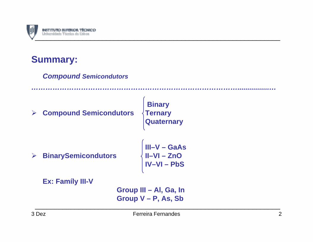
Summary:
Semiconductors. Bonding and band diagrams. Intrinsic and extrinsic
semiconductors. Doping: donors and acceptors.
……………………………………………………………………………………...
Electric Conductivity between (106 -108 S.m-1) and (10-20 -10-8 S.m-1).
______________________________________________________________
Electric Conductivity between (106 -108 S.m-1) and (10-20 -10-8 S.m-1).
Strong temperature dependence in intrinsic semiconductors
Electric properties highly dependent on the inclusion of donor oracceptor impurities (extrinsic semiconductors)
______________________________________________________________2Ferreira Fernandesweek 1 - lesson 2
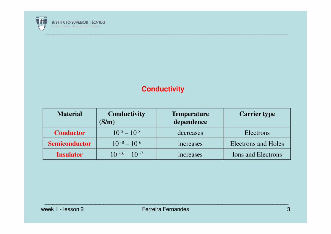
Conductivity
Material Conductivity Temperature Carrier type
______________________________________________________________
Material Conductivity
(S/m)
Temperature
dependence
Carrier type
Conductor 10 5 – 10 8 decreases Electrons
Semiconductor 10 -8 – 10 6 increases Electrons and Holes
Insulator 10 -16 – 10 -7 increases Ions and Electrons
______________________________________________________________3Ferreira Fernandesweek 1 - lesson 2
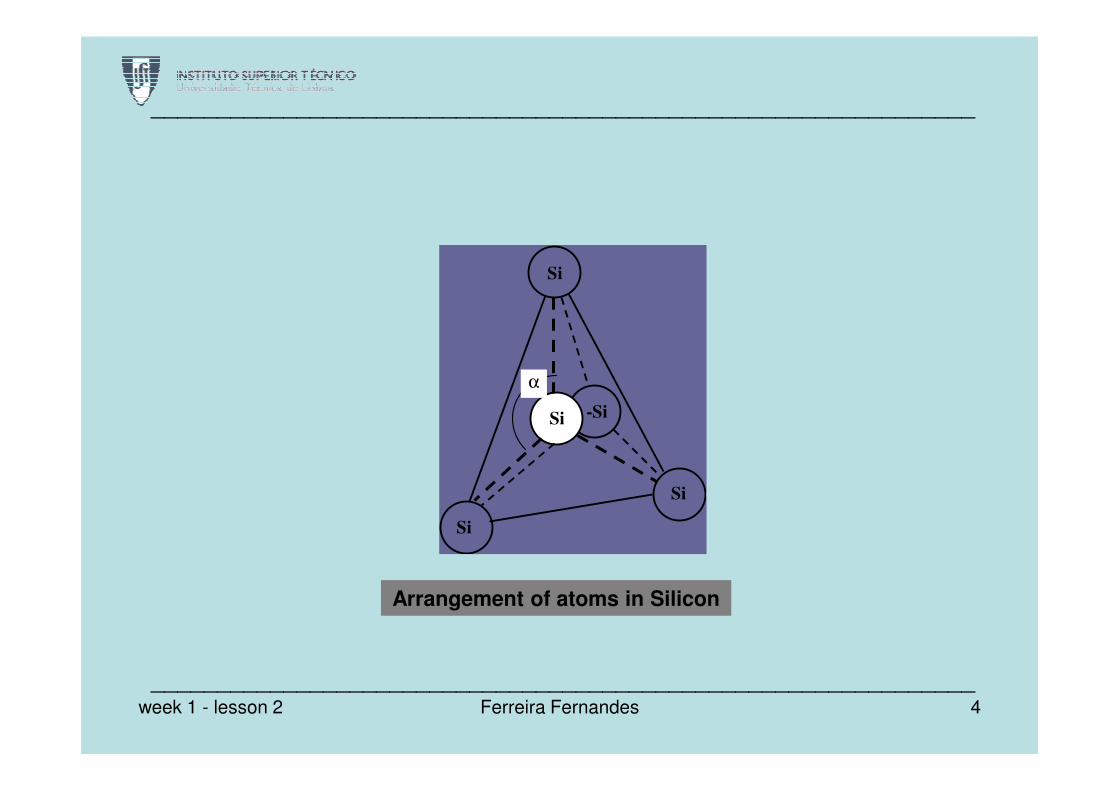
Si
α
______________________________________________________________
-Si Si
Si
Si
Arrangement of atoms in Silicon
______________________________________________________________4Ferreira Fernandesweek 1 - lesson 2
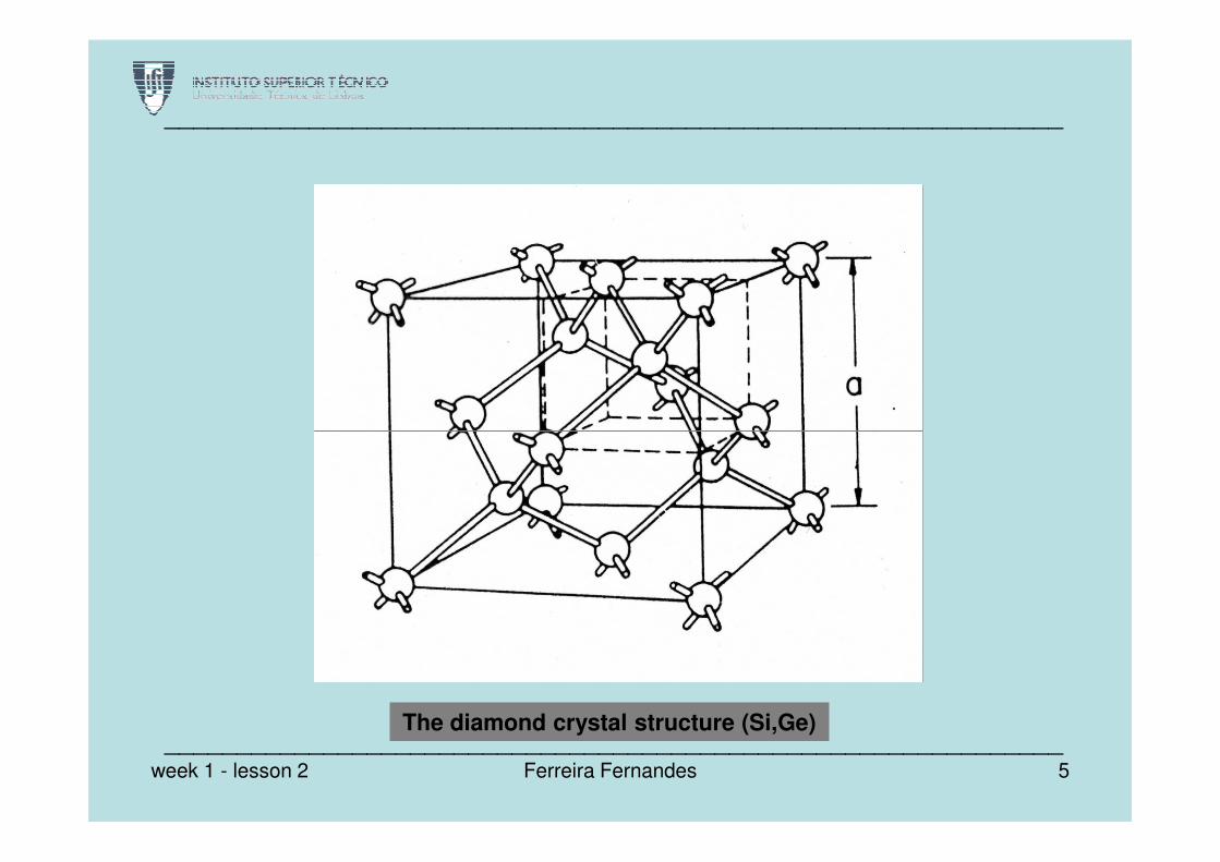
______________________________________________________________
The diamond crystal structure (Si,Ge)
5Ferreira Fernandes
______________________________________________________________week 1 - lesson 2
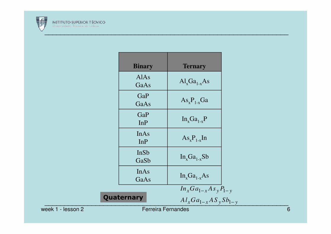
Binary Ternary
AlAs
GaAsAlxGa1-xAs
GaP
GaAsAsxP1-xGa
GaPIn Ga P
______________________________________________________________
GaP
InPInxGa1-xP
InAs
InPAsxP1-xIn
InSb
GaSbInxGa1-xSb
InAs
GaAsInxGa1-xAs
1 1
1 1
x x y y
x x y y
In Ga As P
Al Ga AS Sb
− −
− −Quaternary
______________________________________________________________6Ferreira Fernandesweek 1 - lesson 2
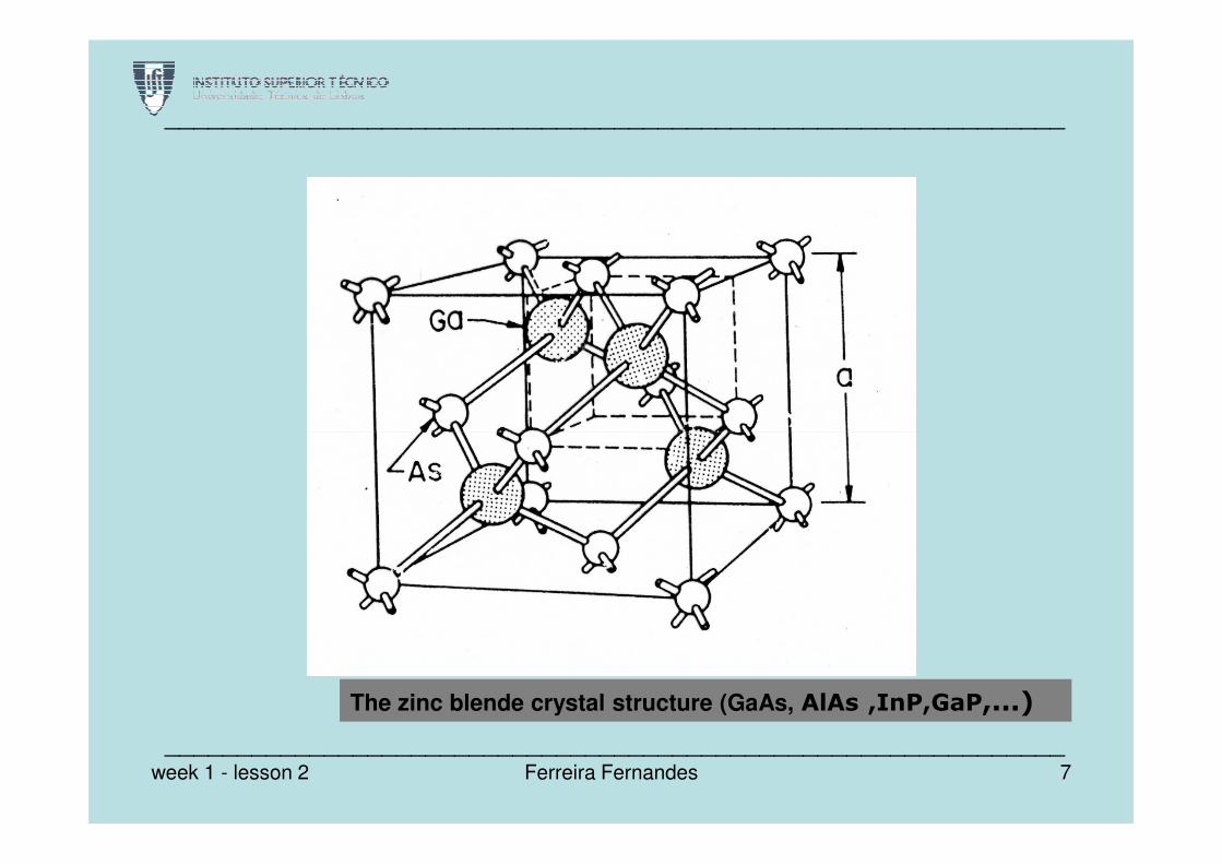
______________________________________________________________
The zinc blende crystal structure (GaAs, AlAs ,InP,GaP,...)
______________________________________________________________7Ferreira Fernandesweek 1 - lesson 2
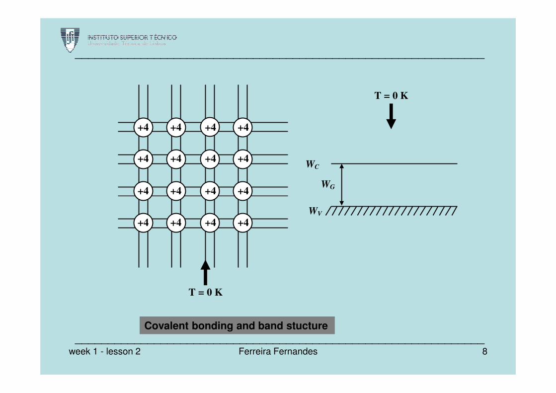
+4 +4 +4 +4
+4 +4 +4 +4
+4 +4 +4 +4
T = 0 K
WC
WG
______________________________________________________________
+4 +4 +4 +4
T = 0 K
WV
Covalent bonding and band stucture______________________________________________________________
8Ferreira Fernandesweek 1 - lesson 2
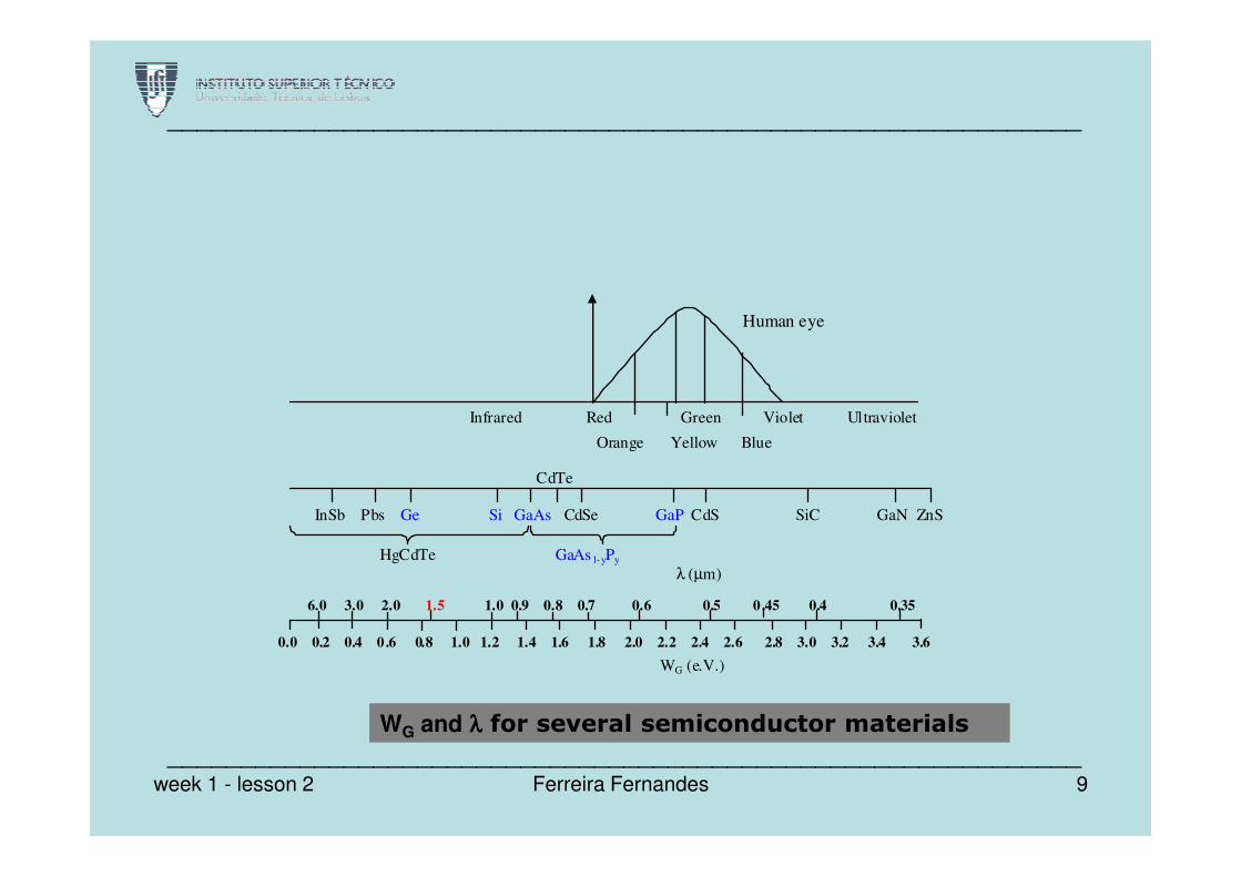
Human eye
Infrared Red Green Violet Ultraviolet
Orange Yellow Blue
______________________________________________________________
WG and λλλλ for several semiconductor materials
Orange Yellow Blue
CdTe
InSb Pbs Ge Si GaAs CdSe GaP CdS SiC GaN ZnS
HgCdTe GaAs1-yPy
λ (µm)
6.0 3.0 2.0 1.5 1.0 0.9 0.8 0.7 0.6 0.5 0 .45 0.4 0.35
0.0 0.2 0.4 0 .6 0.8 1.0 1.2 1.4 1.6 1.8 2.0 2.2 2.4 2.6 2.8 3.0 3.2 3.4 3.6
WG (e.V.)
______________________________________________________________9Ferreira Fernandesweek 1 - lesson 2
+4 +4 +4
+4 +4 +4
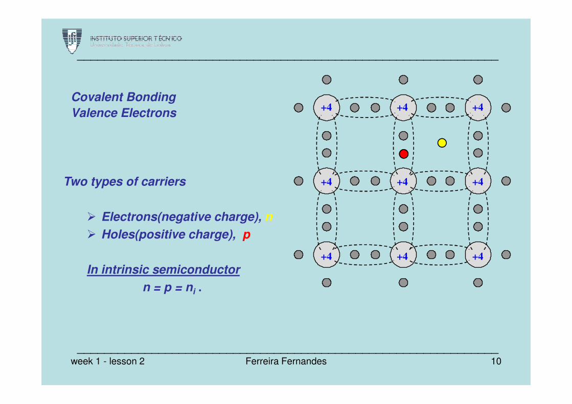
Covalent Bonding
Valence Electrons
Two types of carriers
______________________________________________________________
+4 +4 +4
Electrons(negative charge), n
Holes(positive charge), p
In intrinsic semiconductor
n = p = ni .
______________________________________________________________10Ferreira Fernandesweek 1 - lesson 2
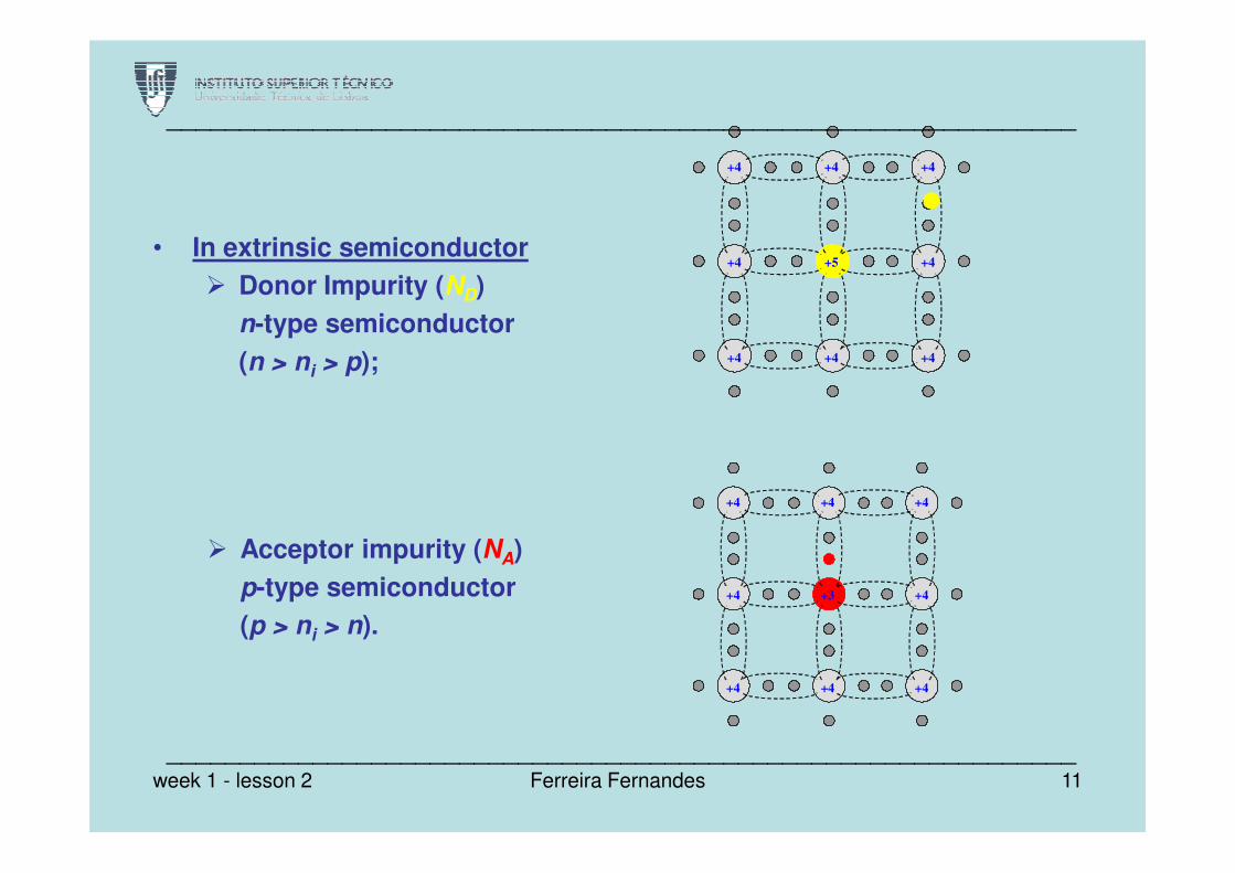
• In extrinsic semiconductor
Donor Impurity (ND)
n-type semiconductor
(n > ni > p);
+4 +4 +4
+4 +5 +4
+4 +4 +4
______________________________________________________________
Acceptor impurity (NA)
p-type semiconductor
(p > ni > n).
+4 +4 +4
+4 +3 +4
+4 +4 +4
11Ferreira Fernandes
______________________________________________________________week 1 - lesson 2
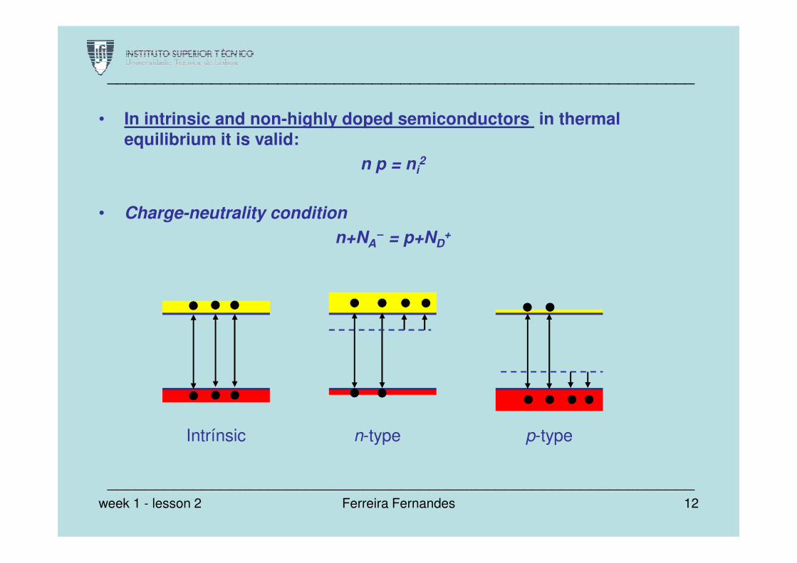
• In intrinsic and non-highly doped semiconductors in thermal equilibrium it is valid:
n p = ni2
• Charge-neutrality condition
n+NA−−−− = p+ND
+
______________________________________________________________
Intrínsic n-type p-type
______________________________________________________________12Ferreira Fernandesweek 1 - lesson 2
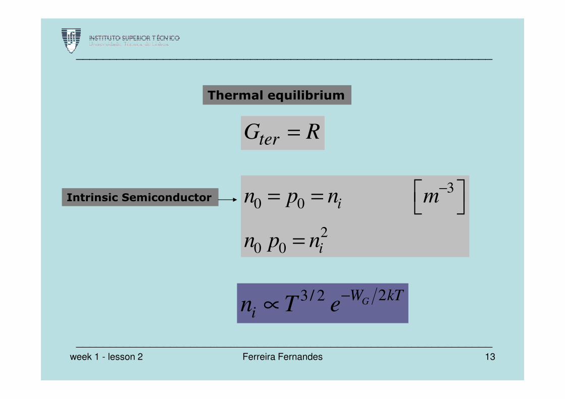
Thermal equilibrium
terG R=
30 0 in p n m
− = = Intrinsic Semiconductor
______________________________________________________________
0 0
20 0
i
i
n p n m
n p n
= =
=
Intrinsic Semiconductor
23/ 2 GW kTin T e
−∝
______________________________________________________________13Ferreira Fernandesweek 1 - lesson 2
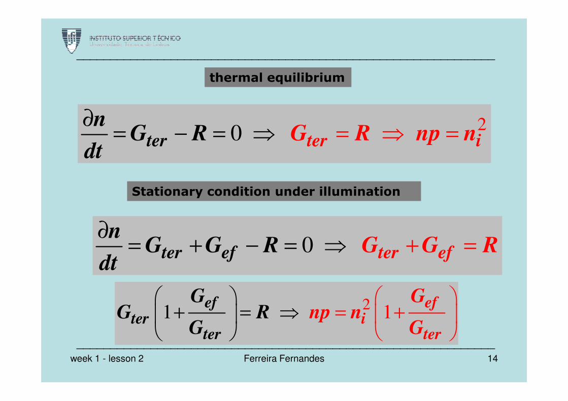
thermal equilibrium
20ter ter iG R np nn
G Rdt
∂= − = ⇒ = ⇒ =
Stationary condition under illumination
______________________________________________________________
21 1ef
iter
efter
ter
Gnp n
G
GG R
G
+ = ⇒
= +
0ter te fe r efn
G G R Gt
G Rd
∂= ++ − = =⇒
______________________________________________________________
14Ferreira Fernandesweek 1 - lesson 2
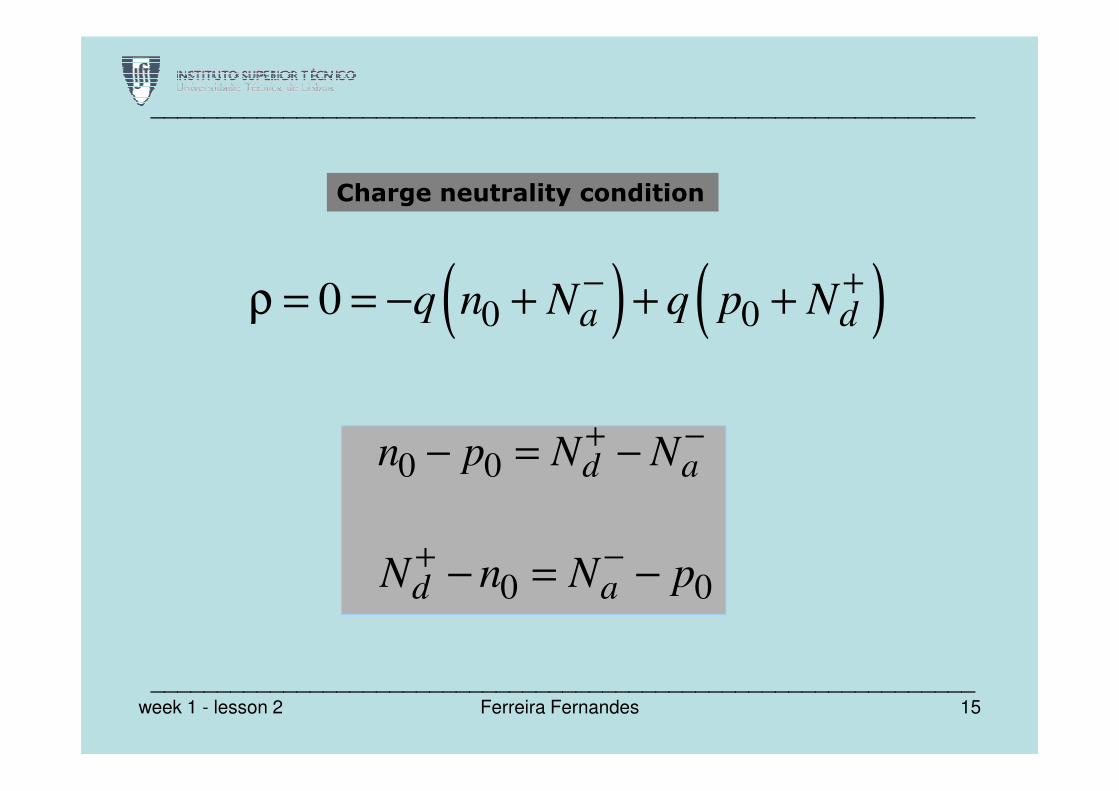
Charge neutrality condition
( ) ( )0 00 a dq n N q p N− +ρ = = − + + +
______________________________________________________________
0 0 d an p N N+ −− = −
0 0d aN n N p+ −− = −
______________________________________________________________15Ferreira Fernandesweek 1 - lesson 2
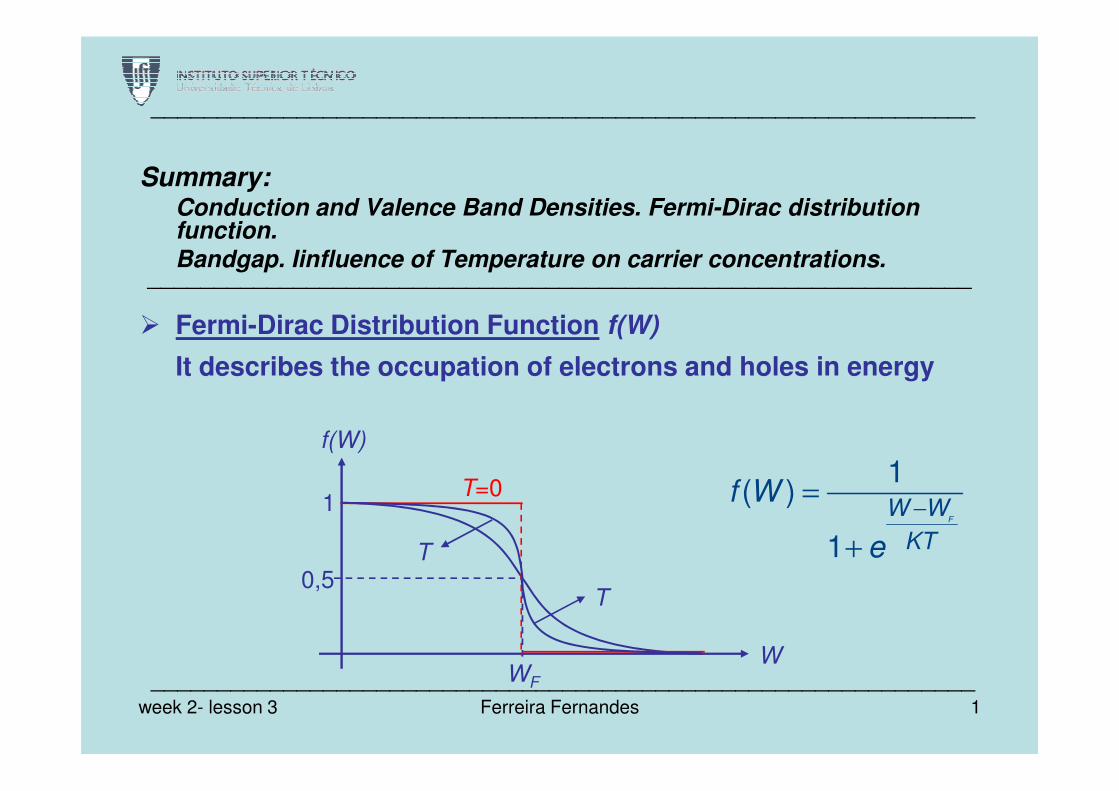
Summary:Conduction and Valence Band Densities. Fermi-Dirac distribution function.
Bandgap. Iinfluence of Temperature on carrier concentrations.
Fermi-Dirac Distribution Function f(W)
It describes the occupation of electrons and holes in energy
______________________________________________________________
______________________________________________________________
1
0,5
f(W)
WF
W
−=
+
1( )
1F
W W
KT
f W
eT
T
T=0
______________________________________________________________1Ferreira Fernandesweek 2- lesson 3
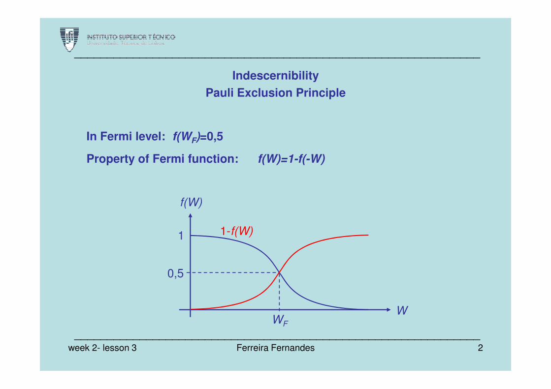
Indescernibility
Pauli Exclusion Principle
In Fermi level: f(WF)=0,5
Property of Fermi function: f(W)=1-f(-W)
______________________________________________________________
f(W)
1
0,5
WF
W
1-f(W)
2Ferreira Fernandes
______________________________________________________________week 2- lesson 3
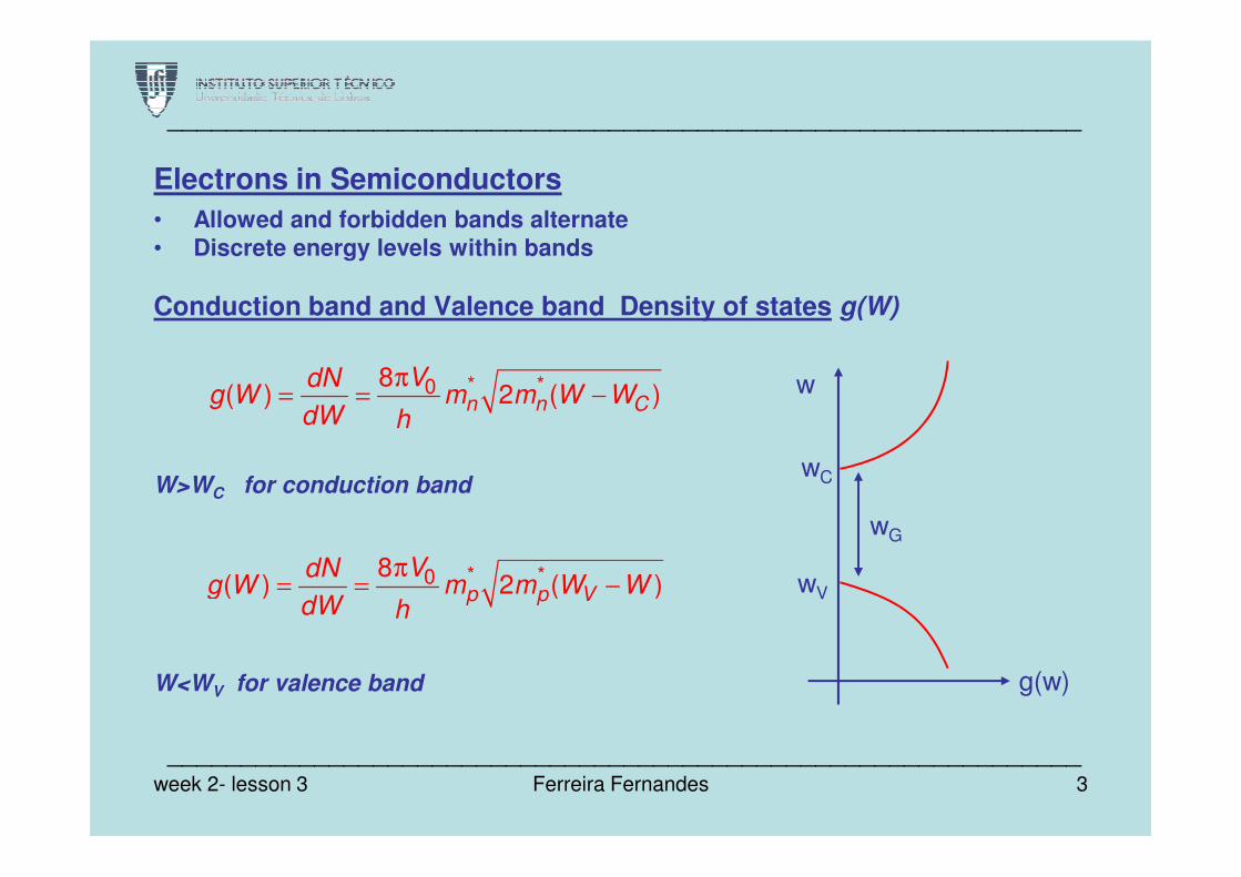
Electrons in Semiconductors
• Allowed and forbidden bands alternate
• Discrete energy levels within bands
Conduction band and Valence band Density of states g(W)
π= = −* *08
( ) 2 ( )n n CVdN
g W m m W WdW h
w
______________________________________________________________
W>WC for conduction band
W<WV for valence band
π= = −* *08
( ) 2 ( )p p VVdN
g W m m W WdW h
wC
wV
g(w)
wG
3Ferreira Fernandes
______________________________________________________________week 2- lesson 3
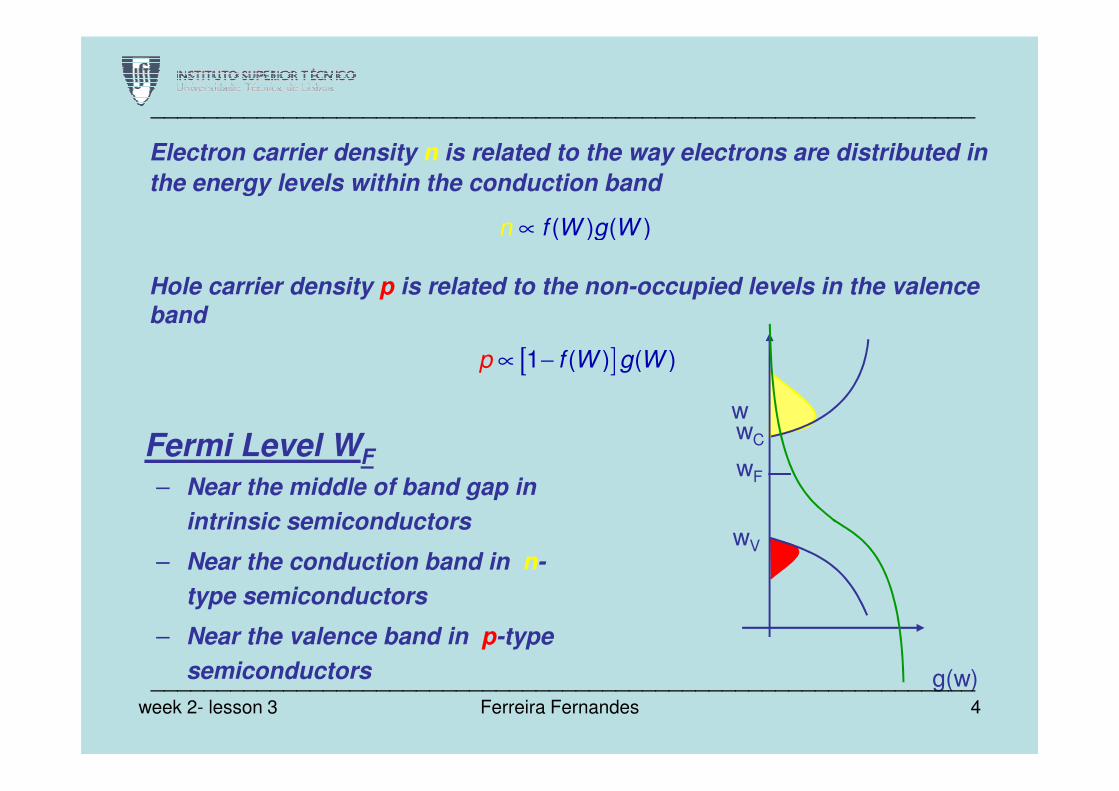
Electron carrier density n is related to the way electrons are distributed in
the energy levels within the conduction band
Hole carrier density p is related to the non-occupied levels in the valence band
∝ ( ) ( )f Wn g W
[ ]∝ −1 ( ) ( )f W g Wp
______________________________________________________________
Fermi Level WF
– Near the middle of band gap in
intrinsic semiconductors
– Near the conduction band in n-
type semiconductors
– Near the valence band in p-type
semiconductors
wwC
wV
g(w)
wF
4Ferreira Fernandes
______________________________________________________________week 2- lesson 3
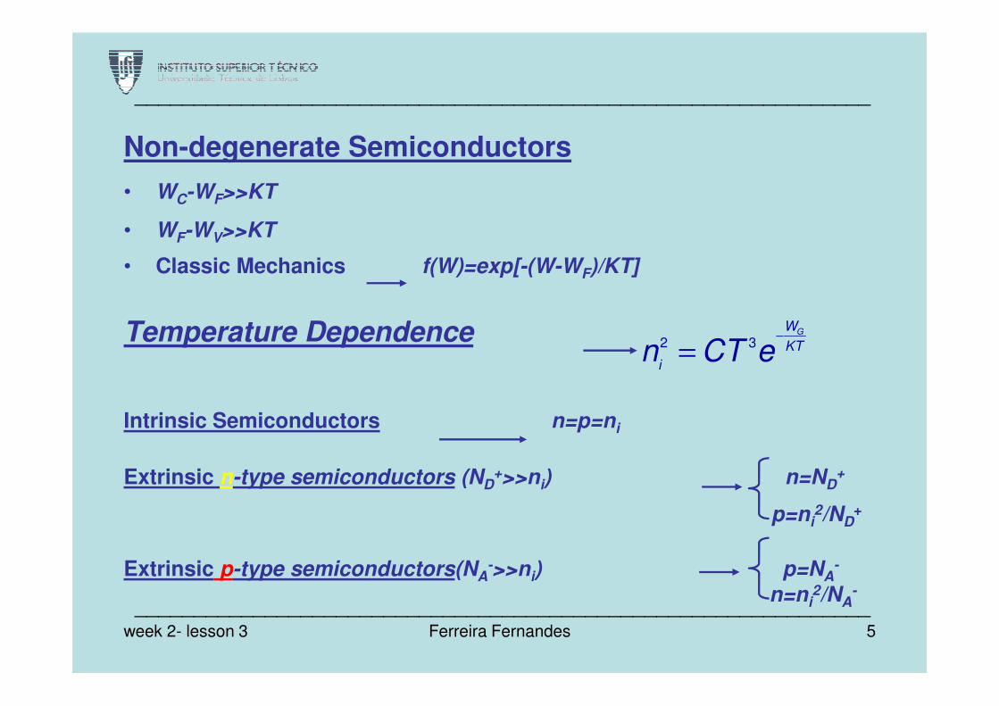
Non-degenerate Semiconductors
• WC-WF>>KT
• WF-WV>>KT
• Classic Mechanics f(W)=exp[-(W-WF)/KT]
Temperature Dependence −
=2 3GW
KTn CT e
______________________________________________________________
Intrinsic Semiconductors n=p=ni
Extrinsic n-type semiconductors (ND+>>ni) n=ND
+
p=ni2/ND
+
Extrinsic p-type semiconductors(NA->>ni) p=NA
-
n=ni2/NA
-
= KT
in CT e
5Ferreira Fernandes
______________________________________________________________week 2- lesson 3
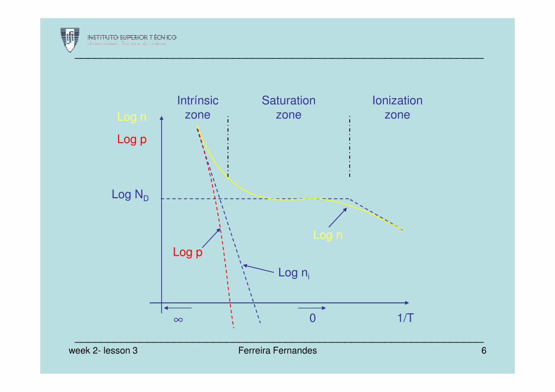
Intrínsic
zone
Saturation
zone
Ionization
zoneLog n
Log p
Log ND
______________________________________________________________
Log ND
Log p
Log n
Log ni
1/T0∞
6Ferreira Fernandes
______________________________________________________________week 2- lesson 3
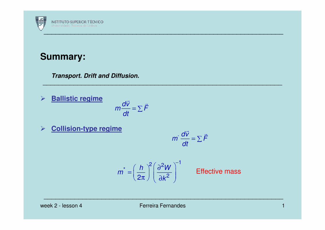
Summary:
Transport. Drift and Diffusion.
Ballistic regime
= ∑
dv
m Fdt
______________________________________________________________
______________________________________________________________
Collision-type regime
dt
= ∑
* dvm F
dt
− ∂
= π ∂
12 2*
22
h Wm
kEffective mass
______________________________________________________________
1Ferreira Fernandesweek 2 - lesson 4
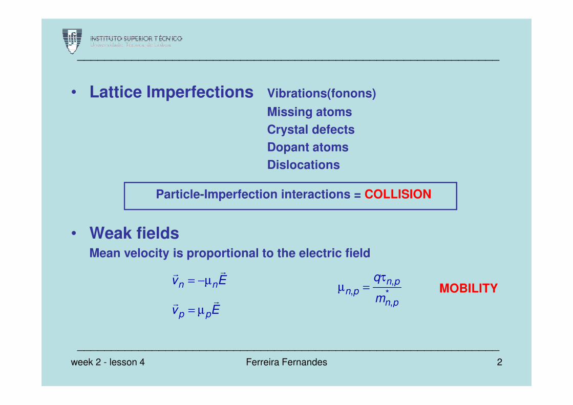
• Lattice Imperfections Vibrations(fonons)
Missing atoms
Crystal defects
Dopant atoms
Dislocations
Particle-Imperfection interactions = COLLISION
______________________________________________________________
• Weak fieldsMean velocity is proportional to the electric field
MOBILITY= −µ
n nv E
= µ
p pv E
τµ =
,, *
,
n pn p
n p
q
m
______________________________________________________________
2Ferreira Fernandesweek 2 - lesson 4
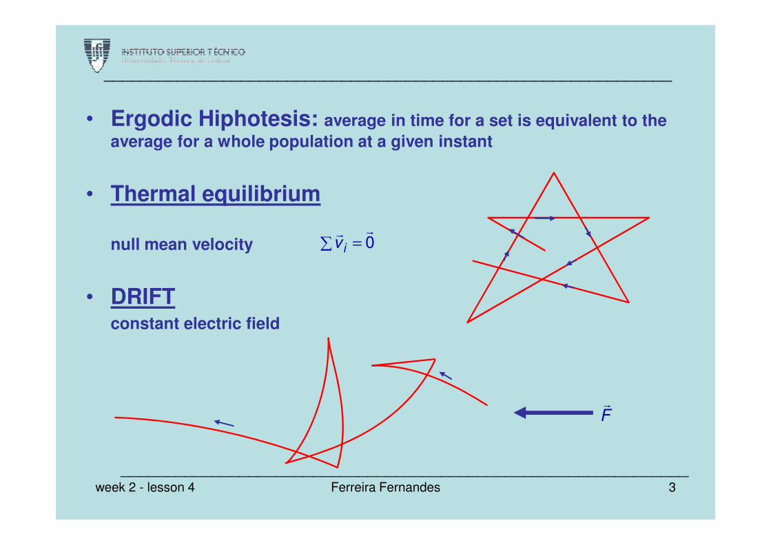
• Ergodic Hiphotesis: average in time for a set is equivalent to the
average for a whole population at a given instant
• Thermal equilibrium
null mean velocity =∑0iv
______________________________________________________________
• DRIFTconstant electric field
F
______________________________________________________________3Ferreira Fernandesweek 2 - lesson 4

• Ohm´s law (local form)
• DIFUSION
= σ
condJ E
( )σ = µ + µn pq n p
= −
C D gradn = −
C D gradp = ×
argJ c a C
CONDUCTIVITY
______________________________________________________________
DIFFUSION COEFFICIENT
• Einstein’s relations
= −
n nC D gradn = −p pC D gradp = ×
argdifJ c a C
= µ = µ, , ,n p n p T n pKT
D Uq
= =( 300 ) 25TU T K mV
______________________________________________________________
4Ferreira Fernandesweek 2 - lesson 4
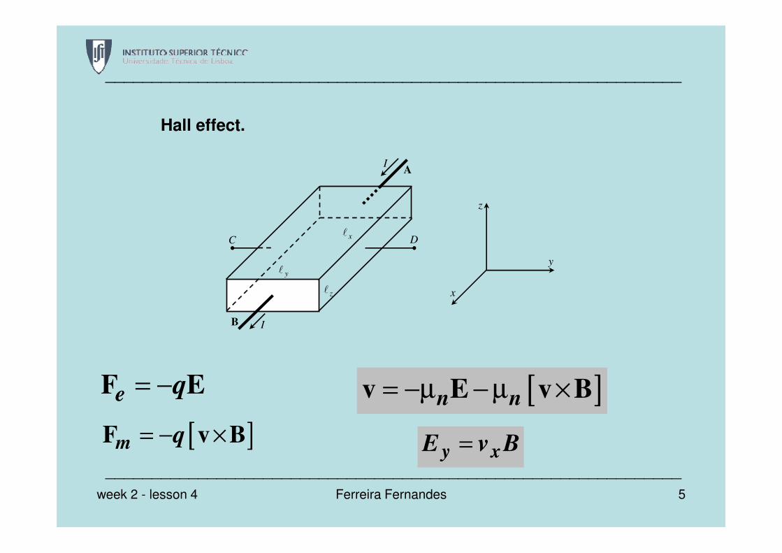
I A
D C
yℓ
xℓ
z
y
Hall effect.
______________________________________________________________
B I
yℓ
zℓ x
e q= −F E
[ ]m q= − ×F v B
[ ]n n= −µ − µ ×v E v B
y xE v B=______________________________________________________________
5Ferreira Fernandesweek 2 - lesson 4
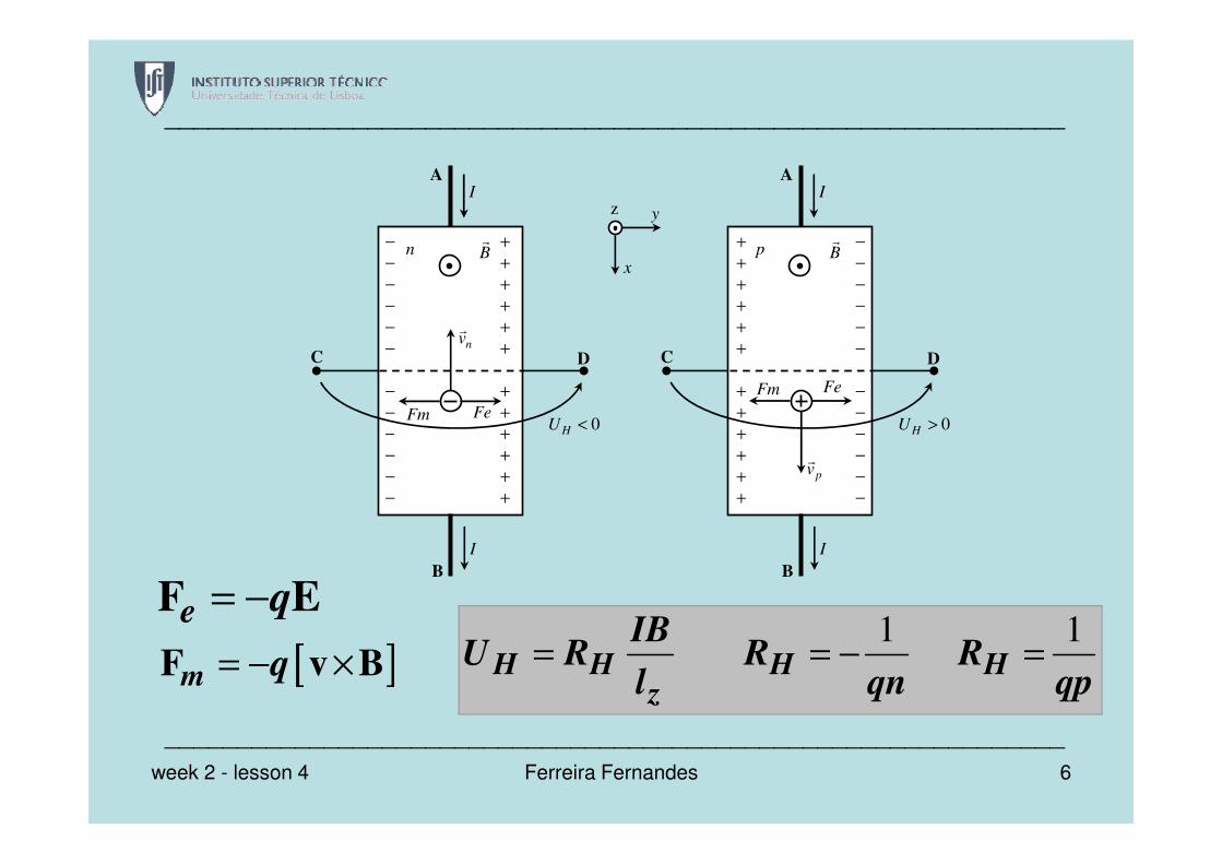
−
−
−
−
−
−
−
−
−
+
+
+
+
+
+
+
+
+
n B
Fm Fe
I A
nv
C D
0HU <
z y
x
−
−
−
−
−
−
−
−
−
+
+
+
+
+
+
+
+
+
p B
Fm Fe
I A
C D
0HU >
______________________________________________________________
−
−
−
−
+
+
+
+
I
B
0HU <−
−
−
−
+
+
+
+
I
B
pv
0HU >
e q= −F E
[ ]m q= − ×F v Bqp
Rqn
Rl
IBRU HH
zHH
11=−==
______________________________________________________________
6Ferreira Fernandesweek 2 - lesson 4
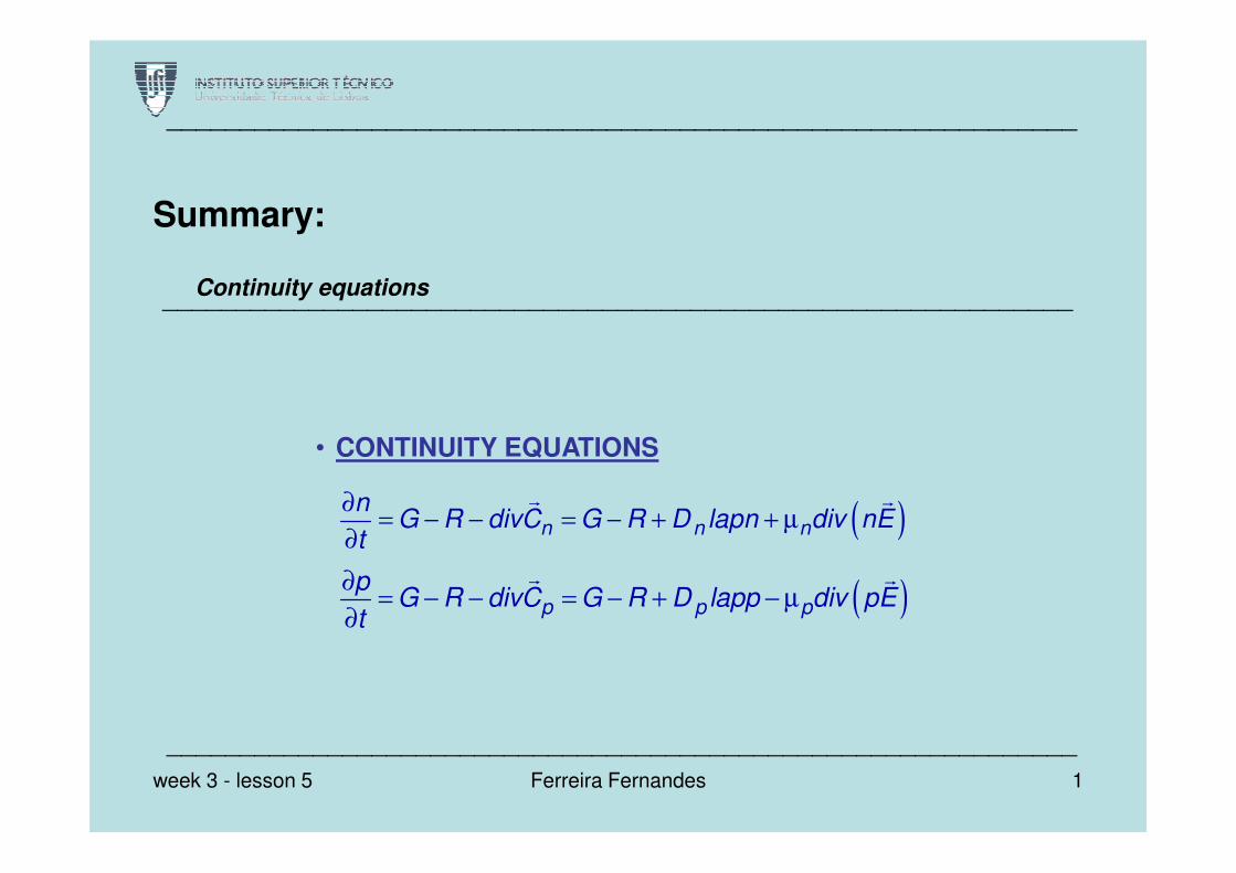
Summary:
Continuity equations
• CONTINUITY EQUATIONS
______________________________________________________________
______________________________________________________________
( )n n nn
G R divC G R D lapn div nEt
∂= − − = − + + µ
∂
( )∂= − − = − + − µ
∂
p p pp
G R divC G R D lapp div pEt
• CONTINUITY EQUATIONS
______________________________________________________________
1Ferreira Fernandesweek 3 - lesson 5
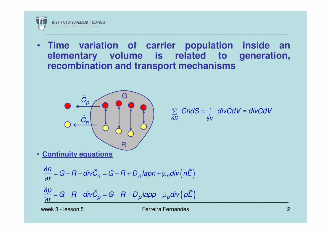
• Time variation of carrier population inside anelementary volume is related to generation,recombination and transport mechanisms
pC
C
G
S V
CndS divCdV divCdVδ δ
= ≅∑ ∫
______________________________________________________________
nC
R
S Vδ δ
( )n n nn
G R divC G R D lapn div nEt
∂= − − = − + + µ
∂
( )∂= − − = − + − µ
∂
p p pp
G R divC G R D lapp div pEt
• Continuity equations
2Ferreira Fernandes
______________________________________________________________
week 3 - lesson 5
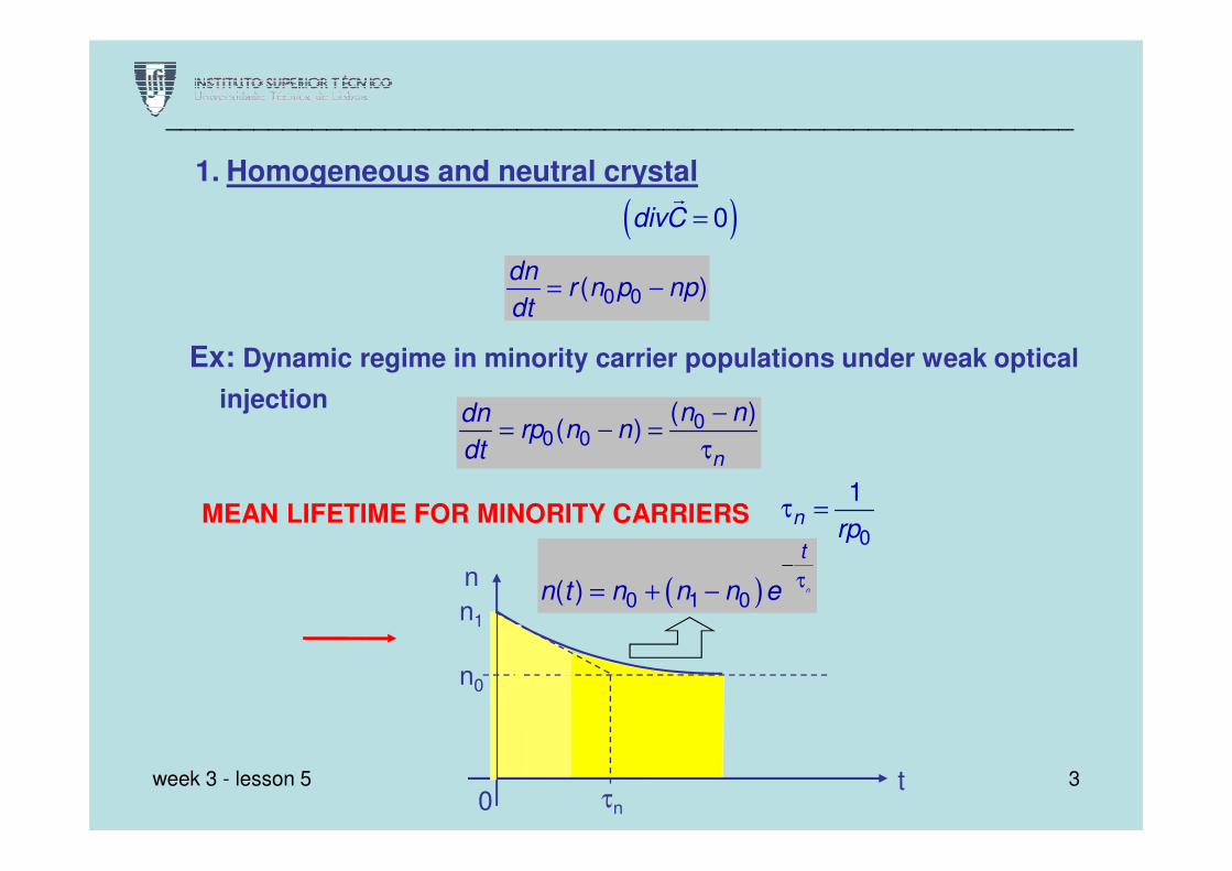
1. Homogeneous and neutral crystal
00 0
( )( )
n ndnrp n n
dt
−= − =
τ
( )0divC =
0 0( )dn
r n p npdt
= −
Ex: Dynamic regime in minority carrier populations under weak optical
injection
______________________________________________________________
0 0( )n
rp n ndt
= − =τ
MEAN LIFETIME FOR MINORITY CARRIERS0
1n
rpτ =
n1
n
n0
τn0t
( )0 1 0( ) n
t
n t n n n e−
τ= + −
3week 3 - lesson 5
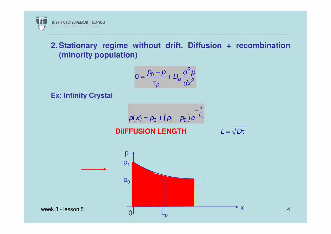
2. Stationary regime without drift. Diffusion + recombination(minority population)
20
20 p
p
p p d pD
dx
−= +
τ
Ex: Infinity Crystal
( )0 1 0( ) p
x
Lp x p p p e
−
= + −
______________________________________________________________
( )0 1 0( ) pL
p x p p p e= + −
DiIFFUSION LENGTH L D= τ
p1
p
p0
Lp0x 4week 3 - lesson 5
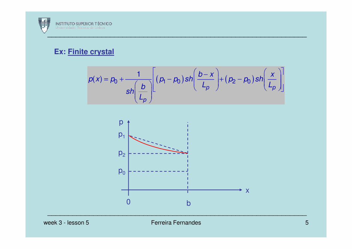
Ex: Finite crystal
( ) ( )0 1 0 2 01
( )p p
p
b x xp x p p p sh p p sh
L Lbsh
L
−= + − + −
p
______________________________________________________________
p
p1
p2
p0
0 b
x
5Ferreira Fernandes
______________________________________________________________
week 3 - lesson 5
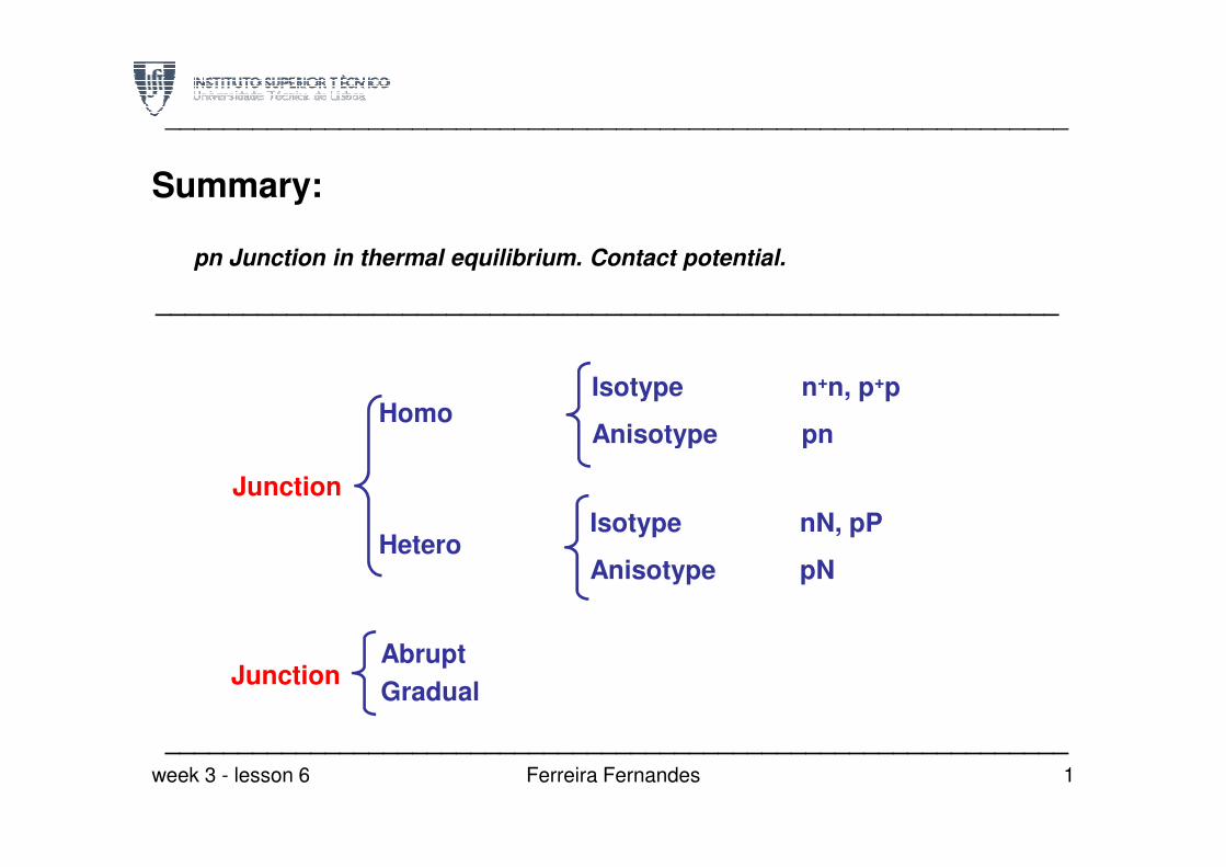
Summary:
pn Junction in thermal equilibrium. Contact potential.
HomoIsotype n+n, p+p
Anisotype pn
______________________________________________________________
______________________________________________________________
Junction
Hetero
Anisotype pn
Isotype nN, pP
Anisotype pN
JunctionAbrupt
Gradual
______________________________________________________________
1Ferreira Fernandesweek 3 - lesson 6
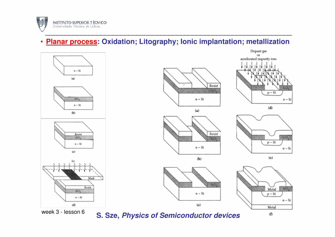
• Planar process: Oxidation; Litography; Ionic implantation; metallization
______________________________________________________________
S. Sze, Physics of Semiconductor devices week 3 - lesson 6
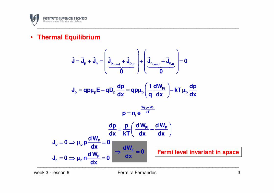
• Thermal Equilibrium
cond df cond dfp n p p n nJ J J J J J J 0
0 0
= + = + + + == + = + + + == + = + + + == + = + + + =
Fip p p p p
dp 1 dW dpJ qp E qD qp kT
dx q dx dx
= µ − = µ − µ= µ − = µ − µ= µ − = µ − µ= µ − = µ − µ
______________________________________________________________
dx q dx dx
Fi FW W
kTip n e
−−−−
====
Fi Fdp p dW dW
dx kT dx dx
= −= −= −= −
F
p p
Fn n
dWJ 0 p 0
dx
dWJ 0 n 0
dx
==== ⇒⇒⇒⇒ µ =µ =µ =µ =
==== ⇒⇒⇒⇒ µ =µ =µ =µ =
FdW0
dx⇒⇒⇒⇒ ==== Fermi level invariant in space
3Ferreira Fernandes
______________________________________________________________
week 3 - lesson 6
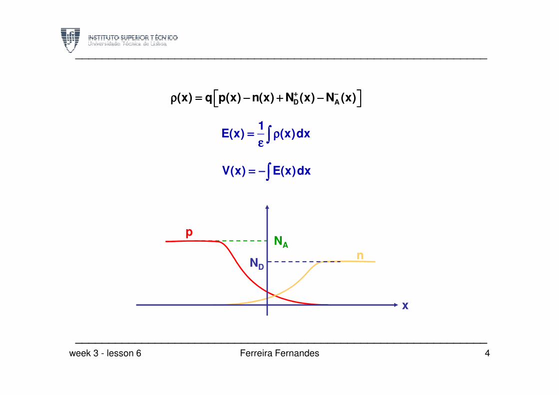
D A(x) q p(x) n(x) N (x) N (x)+ −+ −+ −+ − ρ = − + −ρ = − + −ρ = − + −ρ = − + −
1E(x) (x)dx= ρ= ρ= ρ= ρ
εεεε ∫∫∫∫
V(x) E(x)dx= −= −= −= −∫∫∫∫
______________________________________________________________
NA
ND
n
p
x
4Ferreira Fernandes
______________________________________________________________
week 3 - lesson 6
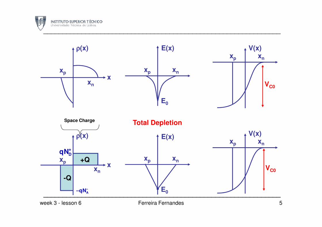
xxp
xn
ρρρρ(x)
xp xn
E(x)
E0
xp xn
V(x)
VC0
______________________________________________________________
xp xn
E(x)
E0
Total Depletion
xp xn
V(x)
VC0x
xp
xn
ρρρρ(x)
DqN++++
AqN−−−−−−−−
+Q
-Q
Space Charge
5Ferreira Fernandes
______________________________________________________________
week 3 - lesson 6
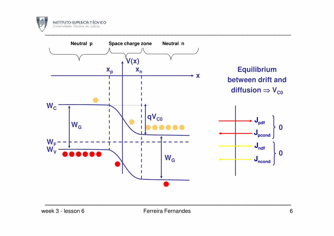
Equilibrium
between drift and
diffusion ⇒⇒⇒⇒ VC0
J
xp xn
V(x)
x
WC
qVC0
Neutral p Neutral nSpace charge zone
______________________________________________________________
pdfJ
pcondJ
ndfJ
ncondJ
0
0
WF
WV
WG
WG
qVC0
6Ferreira Fernandes
______________________________________________________________
week 3 - lesson 6
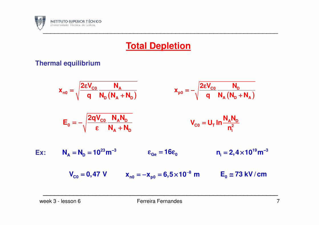
(((( ))))C0 D
p0
A D A
2 V Nx
q N N N
εεεε= −= −= −= −
++++
Total Depletion
Thermal equilibrium
(((( ))))C0 A
n0
D A D
2 V Nx
q N N N
εεεε====
++++
______________________________________________________________
C0 A D0
A D
2qV N NE
N N= −= −= −= −
ε +ε +ε +ε +A D
C0 T 2i
N NV U ln
n====
Ex: 23 3A DN N 10 m−−−−= == == == = Ge 016ε = εε = εε = εε = ε 19 3
in 2,4 10 m−−−−= ×= ×= ×= ×
C0V 0,47 V==== 8n0 p0x x 6,5 10 m−−−−= − = ×= − = ×= − = ×= − = × 0E 73 kV / cm≅≅≅≅
7Ferreira Fernandes
______________________________________________________________
week 3 - lesson 6
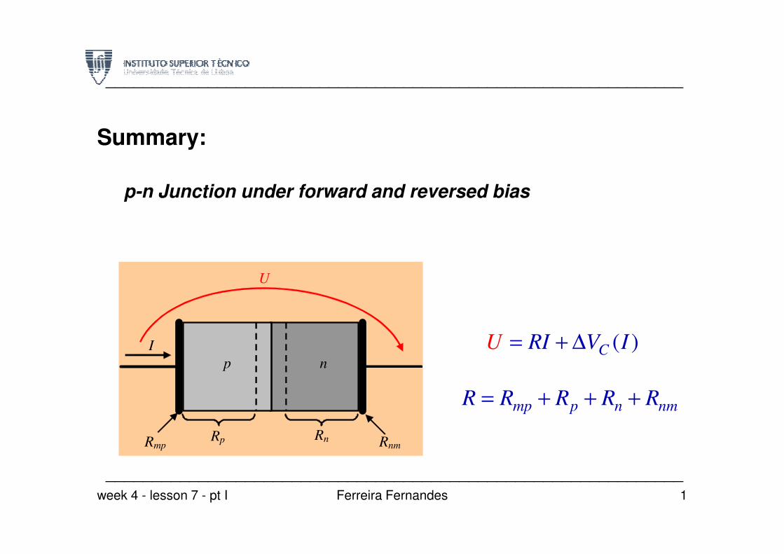
Summary:
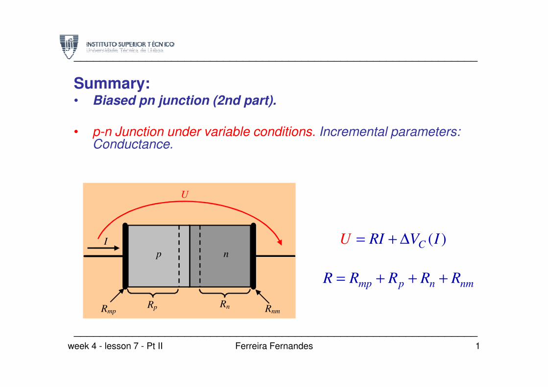
p-n Junction under forward and reversed bias
U
______________________________________________________________
U
I
p n
Rp Rn Rmp Rnm
( )CU RI V I= + ∆
mp p n nmR R R R R= + + +
______________________________________________________________
1Ferreira Fernandesweek 4 - lesson 7 - pt I
Assumed conditions:
• Similar equations for biased p-n and thermal equilibrium for
carrier concentrations.
• Majority concentrations similar to thermal equilibrium. Minority
______________________________________________________________
• Majority concentrations similar to thermal equilibrium. Minority
are deeply influenced by polarization
• Negligible recombination and generation rates in the depletion
region.
2Ferreira Fernandes
______________________________________________________________
week 4 - lesson 7 - pt I
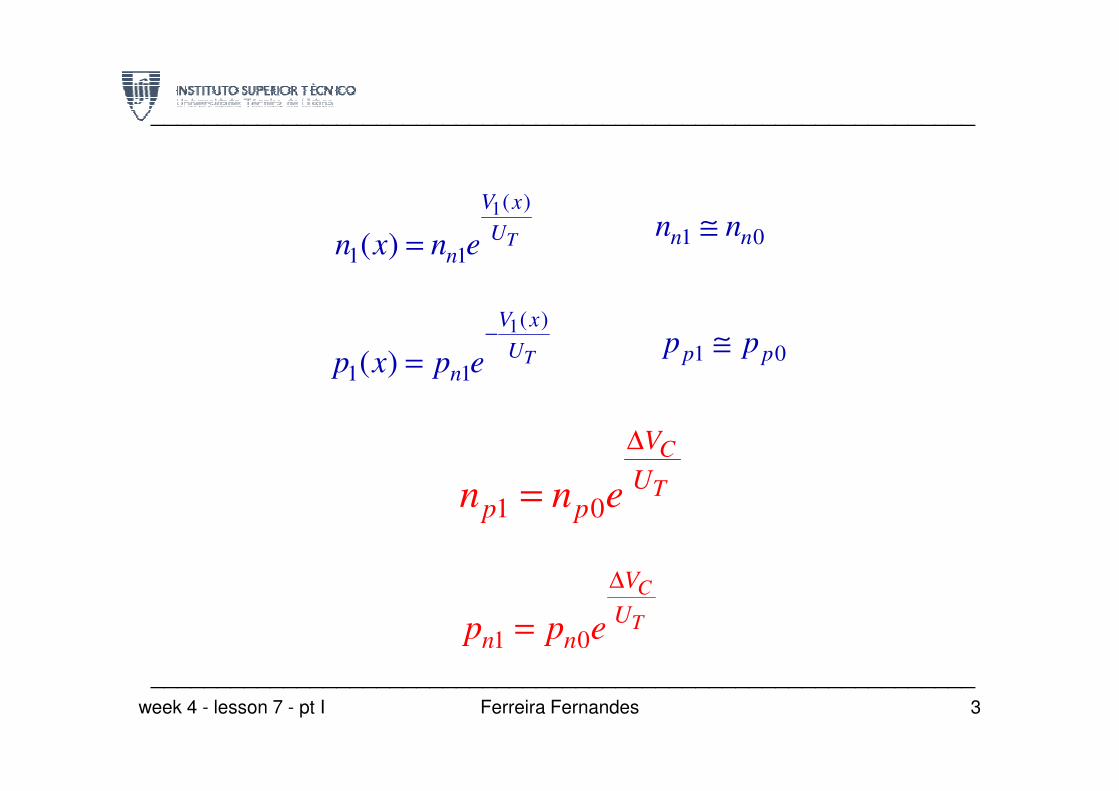
1( )
1 1( ) T
V x
Unn x n e=
1( )
1 1( ) T
V x
Unp x p e
−
=
1 0n nn n≅
1 0p pp p≅
______________________________________________________________
1 0
C
T
V
Up pn n e
∆
=
1 0
C
T
V
Un np p e
∆
=
3Ferreira Fernandes
______________________________________________________________
week 4 - lesson 7 - pt I
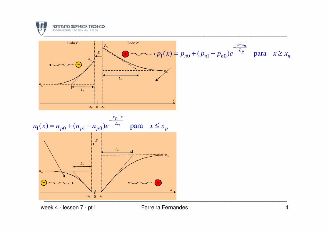
0pn
1np
+
−−−−
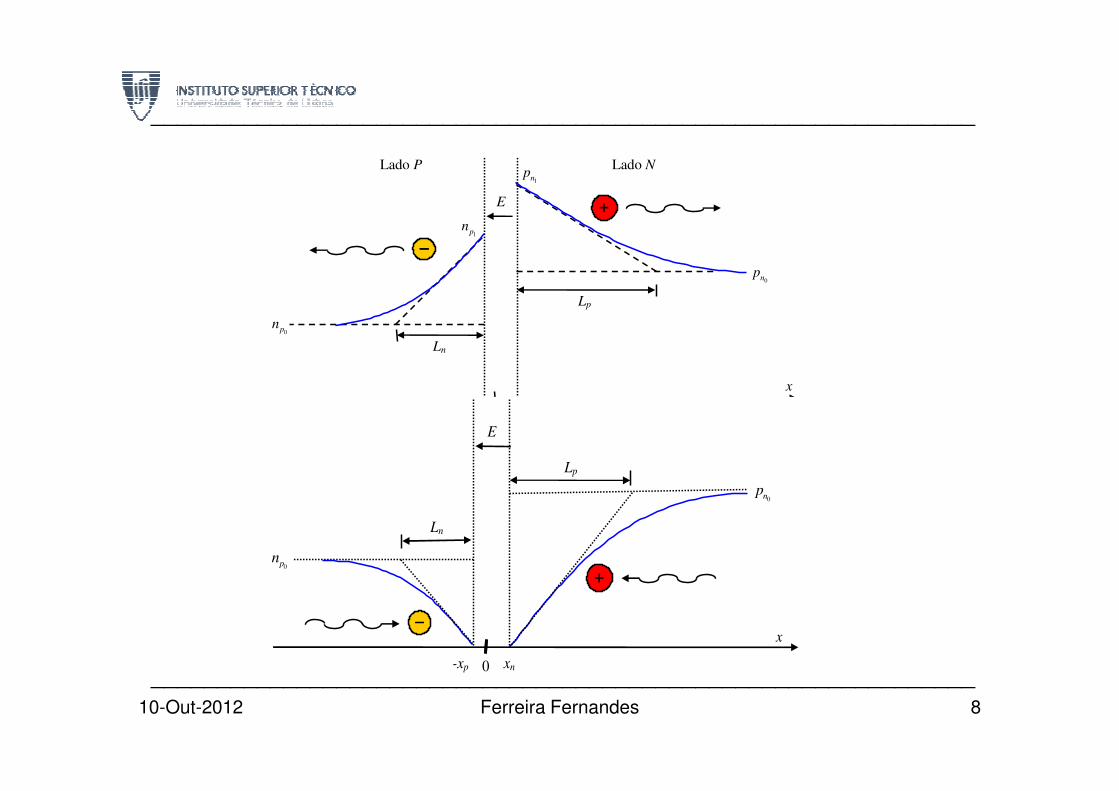
Lado P Lado N
E
Lp
Ln
x
xn -xp 0
1pn
0np
x xp −
1 0 1 0( ) ( ) para
x xnLp
n n n np x p p p e x x
−−
= + − ≥
______________________________________________________________
0pn
E
Lp
Ln
x
xn -xp 0
0np
−−−− +
1 0 1 0( ) ( ) para
x xp
Lnp p p pn x n n n e x x
−−
= + − ≤
4Ferreira Fernandes
______________________________________________________________
week 4 - lesson 7 - pt I
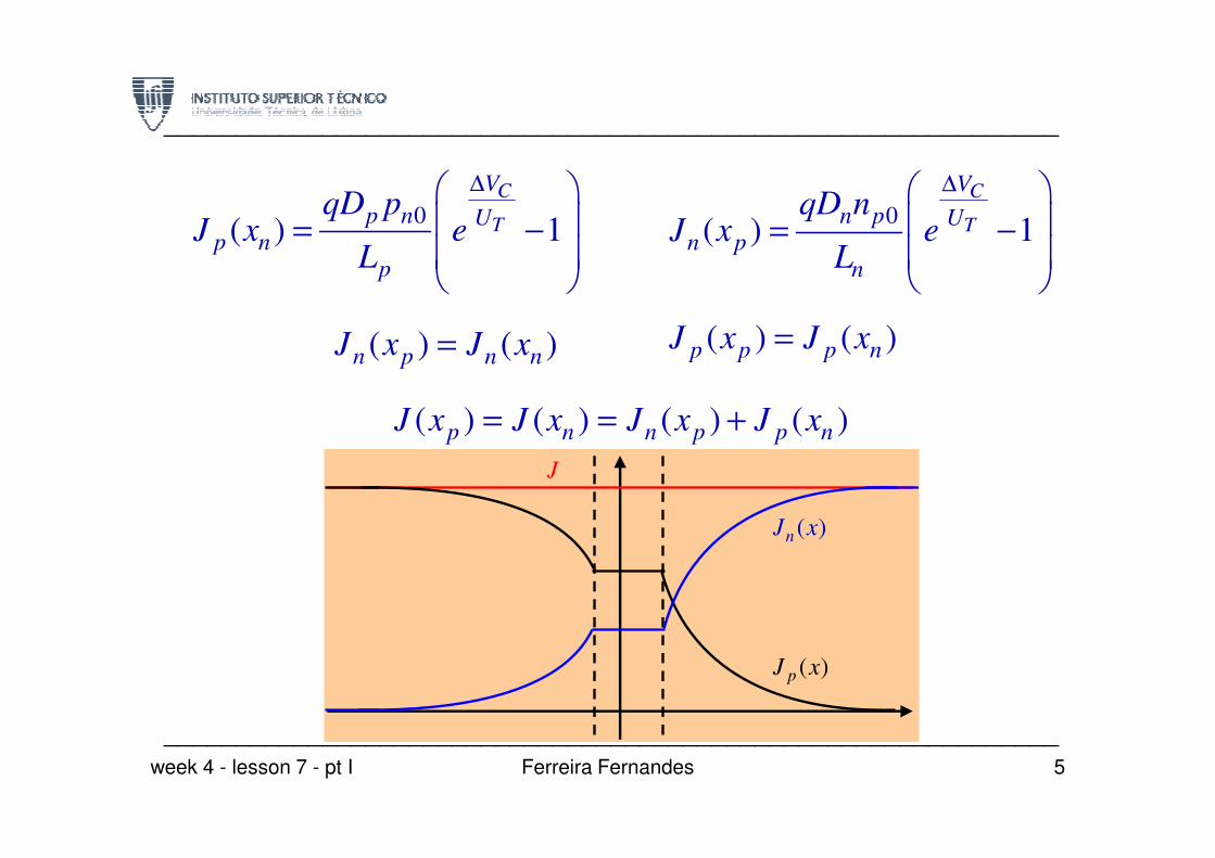
0( ) 1
C
T
V
p n Up n
p
qD pJ x e
L
∆ = −
0( ) 1
C
T
V
n p Un p
n
qD nJ x e
L
∆ = −
( ) ( )n p n nJ x J x= ( ) ( )p p p nJ x J x=
( ) ( ) ( ) ( )p n n p p nJ x J x J x J x= = +
______________________________________________________________
( ) ( ) ( ) ( )p n n p p nJ x J x J x J x= = +
( )nJ x
( )pJ x
J
5Ferreira Fernandes
______________________________________________________________
week 4 - lesson 7 - pt I
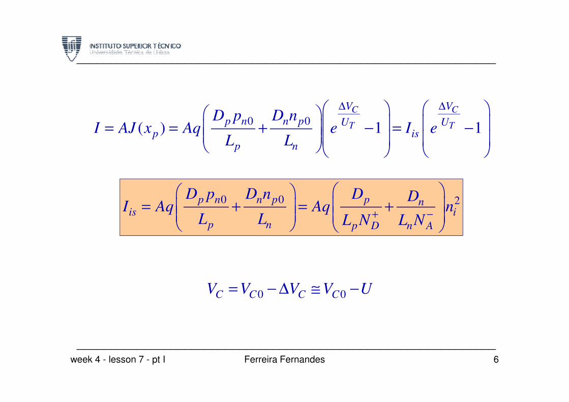
0 0( ) 1 1
C C
T T
V V
p n n p U Up is
p n
D p D nI AJ x Aq e I e
L L
∆ ∆ = = + − = −
0 0 2p n n p p nD p D n D D
I Aq Aq n
= + = +
______________________________________________________________
0 0 2p n n p p nis i
p n p D n A
D p D n D DI Aq Aq n
L L L N L N+ −
= + = +
0 0C C C CV V V V U= − ∆ ≅ −
6Ferreira Fernandes
______________________________________________________________
week 4 - lesson 7 - pt I
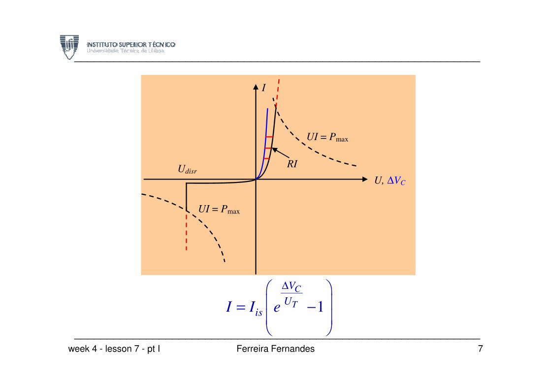
UI = Pmax
I
U, ∆VC Udisr
RI
______________________________________________________________
UI = Pmax
1
C
T
V
UisI I e
∆ = −
7Ferreira Fernandes
______________________________________________________________
week 4 - lesson 7 - pt I
Summary:• Biased pn junction (2nd part).
• p-n Junction under variable conditions. Incremental parameters: Conductance.
U
______________________________________________________________
U
I
p n
Rp Rn Rmp Rnm
( )CU RI V I= + ∆
mp p n nmR R R R R= + + +
______________________________________________________________
1Ferreira Fernandesweek 4 - lesson 7 - Pt II
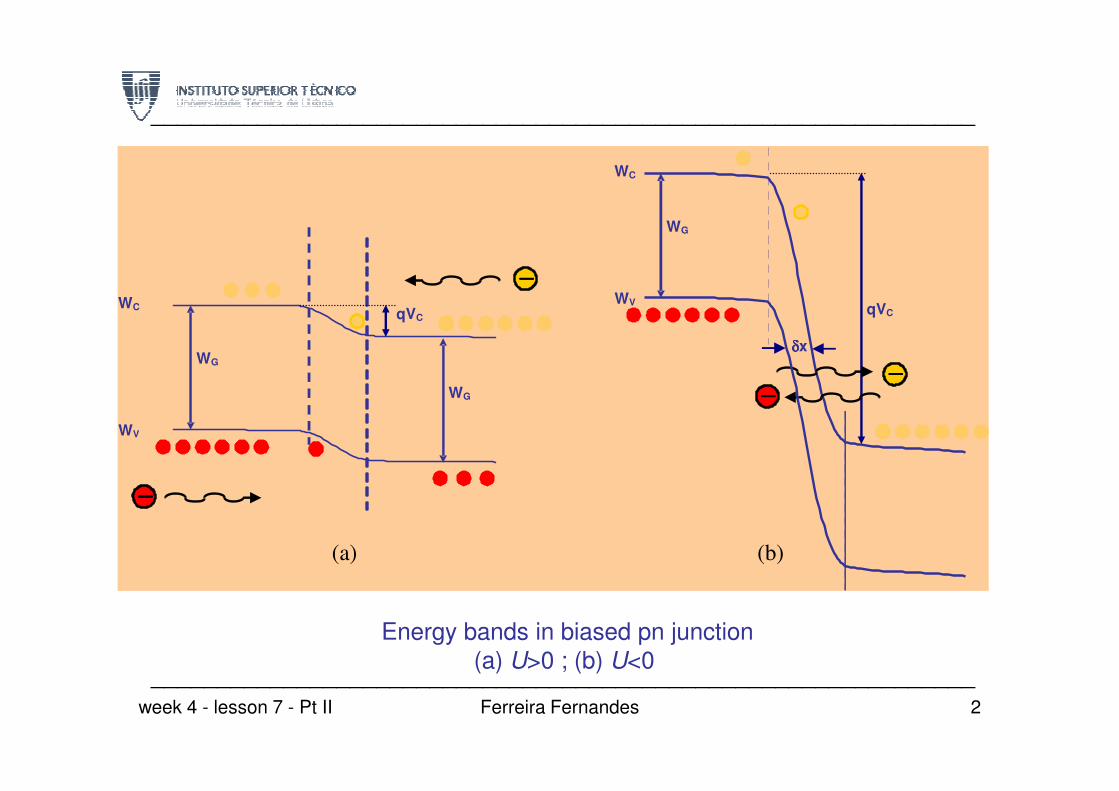
WC
WG
qVC
WG
−−−−
WC
WV
WG
qVC
−−−− −−−−
δδδδx
______________________________________________________________
WV
WG
−−−−
−−−−
(a) (b)
Energy bands in biased pn junction
(a) U>0 ; (b) U<0
2Ferreira Fernandes
______________________________________________________________
week 4 - lesson 7 - Pt II
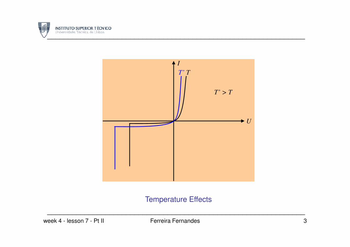
I
U
T’ T
T’ > T
______________________________________________________________
U
Temperature Effects
3Ferreira Fernandes
______________________________________________________________
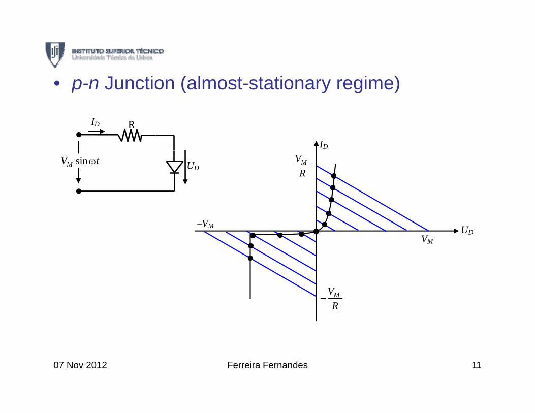
week 4 - lesson 7 - Pt II
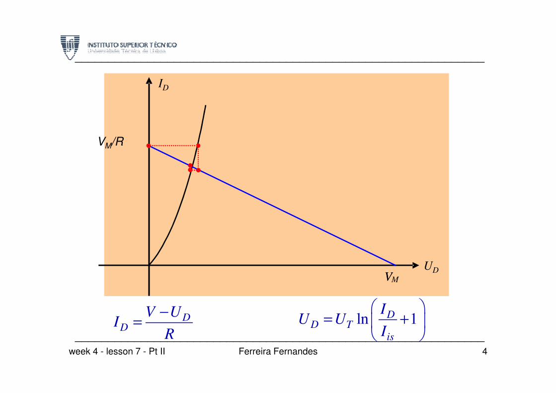
VM/R
ID
______________________________________________________________
DD
V UI
R
−= ln 1
DD T
is
IU U
I
= +
UDVVM
4Ferreira Fernandes
______________________________________________________________
week 4 - lesson 7 - Pt II
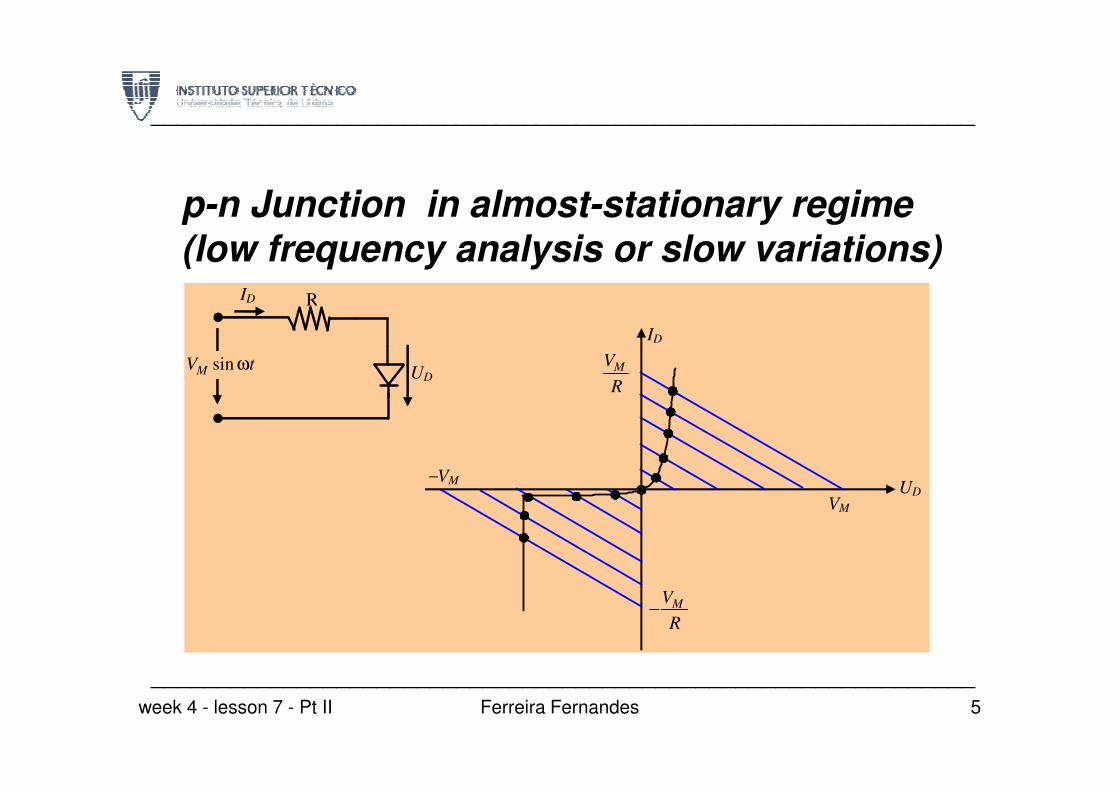
ID
MV
R
ID R
UD sin ωMV t
p-n Junction in almost-stationary regime
(low frequency analysis or slow variations)
______________________________________________________________
UD
VM
−VM
R
− MV
R
5Ferreira Fernandes
______________________________________________________________
week 4 - lesson 7 - Pt II
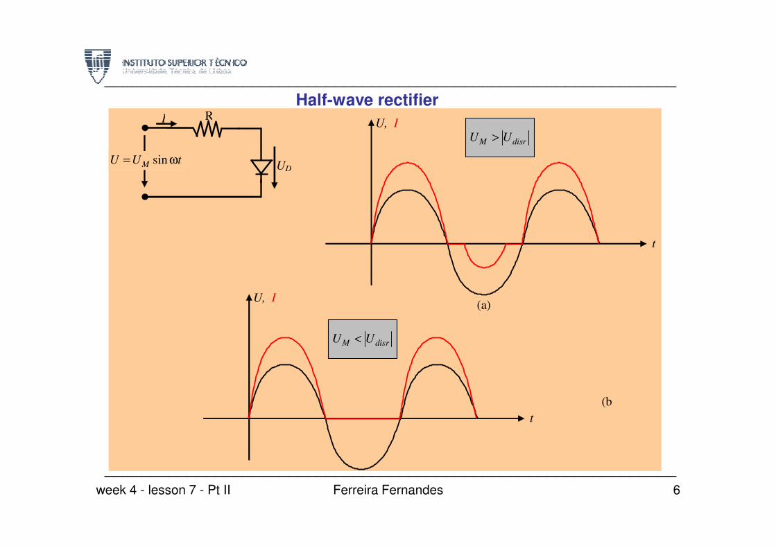
U, I I R
UD sin= ωMU U t
t
>M disrU U
Half-wave rectifier
______________________________________________________________
U, I
t
<M disrU U
(a)
(b
6Ferreira Fernandes
______________________________________________________________
week 4 - lesson 7 - Pt II
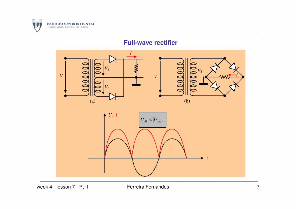
V
VS
VS
I
I V
VS
(a) (b)
Full-wave rectifier
______________________________________________________________
U, I
t
<M disrU U
7Ferreira Fernandes
______________________________________________________________
week 4 - lesson 7 - Pt II
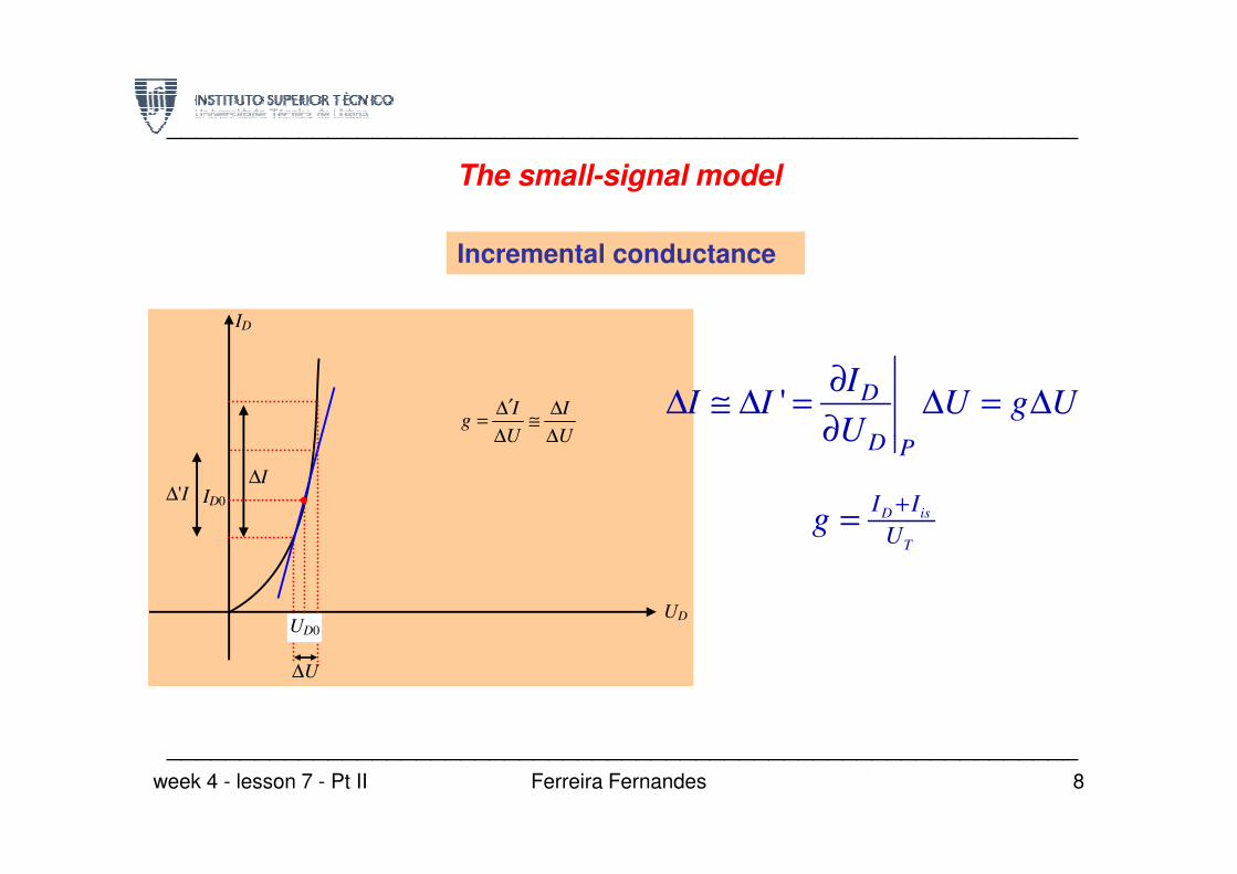
The small-signal model
ID
I Ig
U U
′∆ ∆= ≅
∆ ∆
Incremental conductance
'D
D P
II I U g U
U
∂∆ ≅ ∆ = ∆ = ∆
∂
______________________________________________________________
UD
ID0
UD0
∆U
∆'I ∆I
U U∆ ∆ D PU∂
D is
T
I I
Ug
+=
8Ferreira Fernandes
______________________________________________________________
week 4 - lesson 7 - Pt II
Summary (course 8):Dynamic analysis of p-n junction . Incremental circuit.
Incremental parameters. Conductance and differential capacitances.
______________________________________________________________
10-Out-2012 Ferreira Fernandes 1
U
I
p n
Rp Rn Rmp Rnm
______________________________________________________________
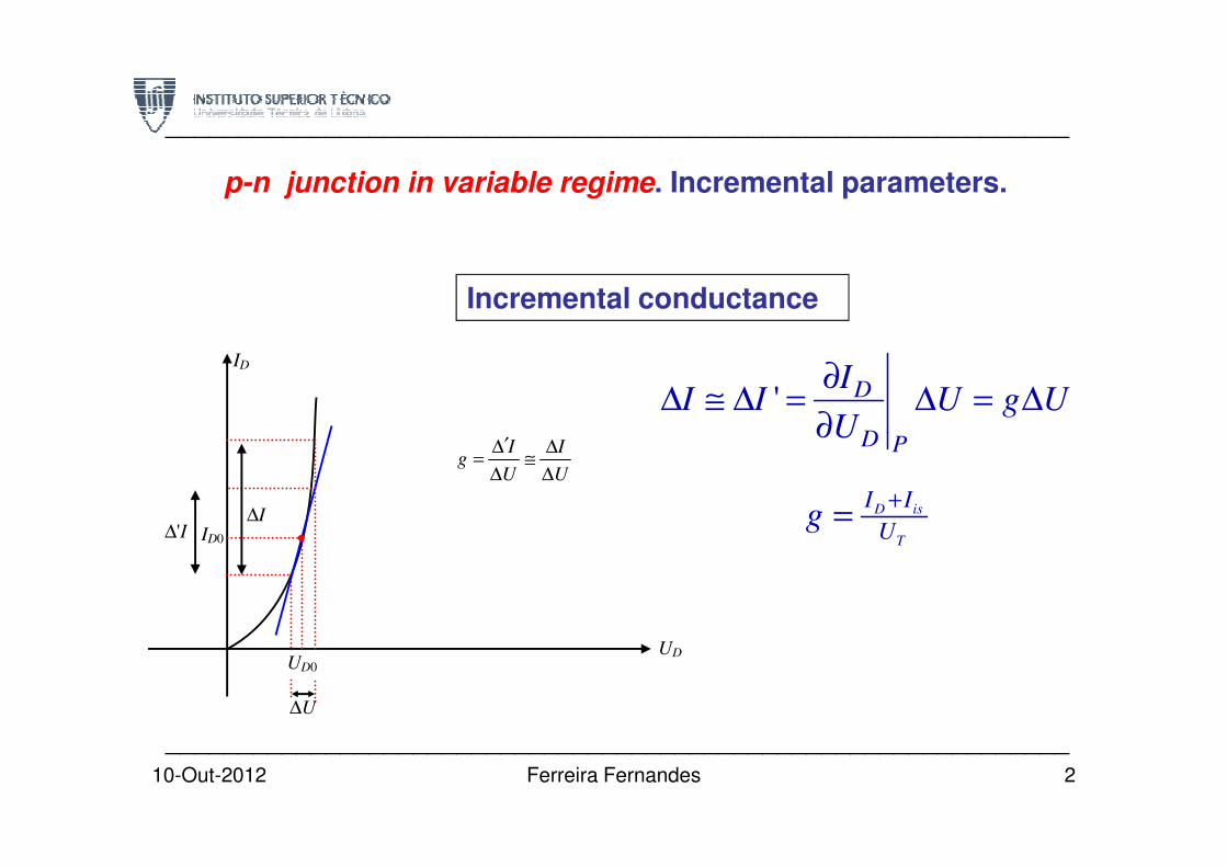
p-n junction in variable regime. Incremental parameters.
ID
Incremental conductance
' D
D P
II I U g U
U
∂∆ ≅ ∆ = ∆ = ∆
∂
______________________________________________________________
UD
ID0
UD0
∆U
∆'I ∆I
I Ig
U U
′∆ ∆= ≅
∆ ∆
D PU∂
D is
T
I I
Ug
+=
2Ferreira Fernandes
______________________________________________________________
10-Out-2012
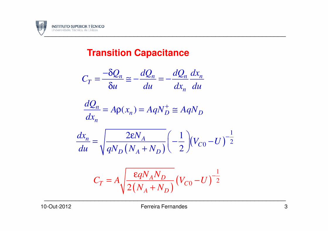
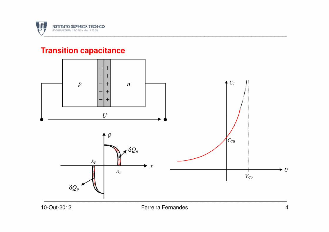
Transition Capacitance
n n n nT
n
Q dQ dQ dxC
u du dx du
−δ= ≅ − = −
δ
( )nn D D
dQA x AqN AqN
dx
+= ρ = ≅
______________________________________________________________
10-Out-2012 Ferreira Fernandes 3
n D D
ndx
( )( )
1
20
2 1
2
n AC
D A D
dx NV U
du qN N N
−ε = − −
+
( )( )
1
202
A DT C
A D
qN NC A V U
N N
−ε= −
+______________________________________________________________
______________________________________________________________
−
−
− −
−
+
+
+ +
+
p n
U
CT
Transition capacitance
10-Out-2012 Ferreira Fernandes 4
______________________________________________________________
U
ρ
x xn
xp
δQn
δQp
U
CT0
VC0
______________________________________________________________
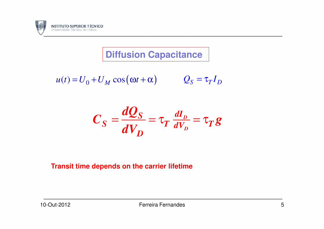
Diffusion Capacitance
( )0( ) cosMu t U U t= + ω + α = τS T DQ I
DdISdQC g= = τ = τ
10-Out-2012 Ferreira Fernandes 5
______________________________________________________________
D
D
dISS T TdV
D
dQC g
dV= = τ = τ
Transit time depends on the carrier lifetime
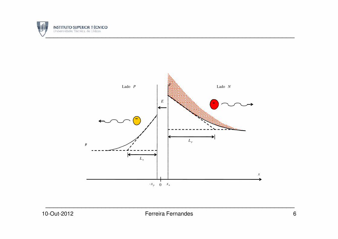
______________________________________________________________
1np
+
−−−−
Lado P Lado N
E
10-Out-2012 Ferreira Fernandes 6
______________________________________________________________
0pn
−−−−
L p
L n
x
x n-x p 0
______________________________________________________________
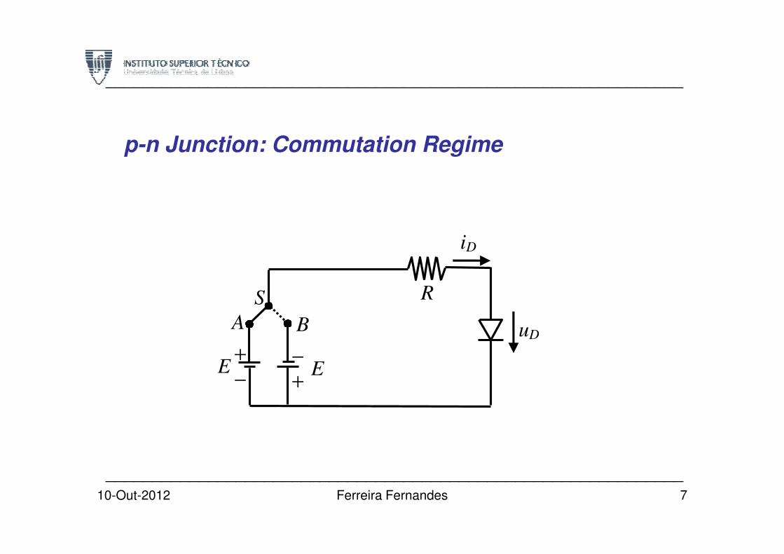
p-n Junction: Commutation Regime
iD
10-Out-2012 Ferreira Fernandes 7
______________________________________________________________
uD
− + −
+
A B
S
E E
R
______________________________________________________________
0pn
1np
+
−−−−
Lado P Lado N
E
Lp
Ln
x
1pn
0np
10-Out-2012 Ferreira Fernandes 8
______________________________________________________________
xn -xp 0
0pn
E
Lp
Ln
x
xn -xp 0
0np
+
−−−−
______________________________________________________________
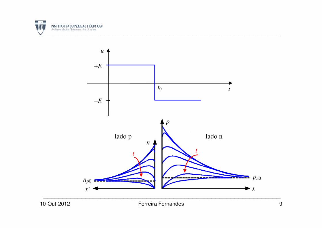
u
t t0
−E
+E
10-Out-2012 Ferreira Fernandes 9
______________________________________________________________
lado n lado p n
p
x x’
pn0 np0
t t
______________________________________________________________
−−−−
Stationary characteristic I(U) for a Si diode
Summary (courses 9 and 10):Si p-n junction. Stationary characteristic I(U).
15 e 17-Out-2012 Ferreira Fernandes 1
______________________________________________________________
(i) For reversed bias, the current does not saturates in −−−−Iis
(i) For forward bias, the current increase with voltage is slower, for small
currents.
______________________________________________________________
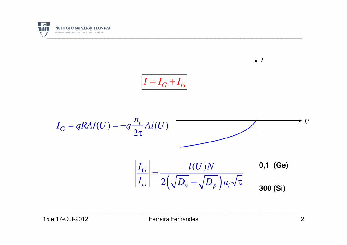
( ) ( )inI qRAl U q Al U= = −
I
U
G isI I I= +
15 e 17-Out-2012 Ferreira Fernandes 2
______________________________________________________________
( ) ( )2
iG
nI qRAl U q Al U= = −
τ
( )( )
2
G
is n p i
I l U N
I D D n=
+ τ
0,1 (Ge)
300 (Si)
U
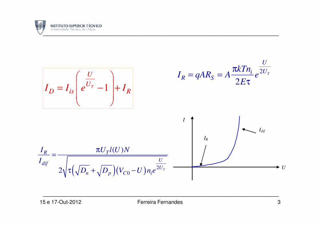
______________________________________________________________
2
2T
U
UiR S
kTnI qAR A e
E
π= =
τ1T
U
UD is RI I e I
= − +
15 e 17-Out-2012 Ferreira Fernandes 3
______________________________________________________________
( )( ) 20
( )
2 T
R T
Udif
Un p C i
I U l U N
I
D D V U n e
π=
τ + −
IR
Idif
I
U
______________________________________________________________
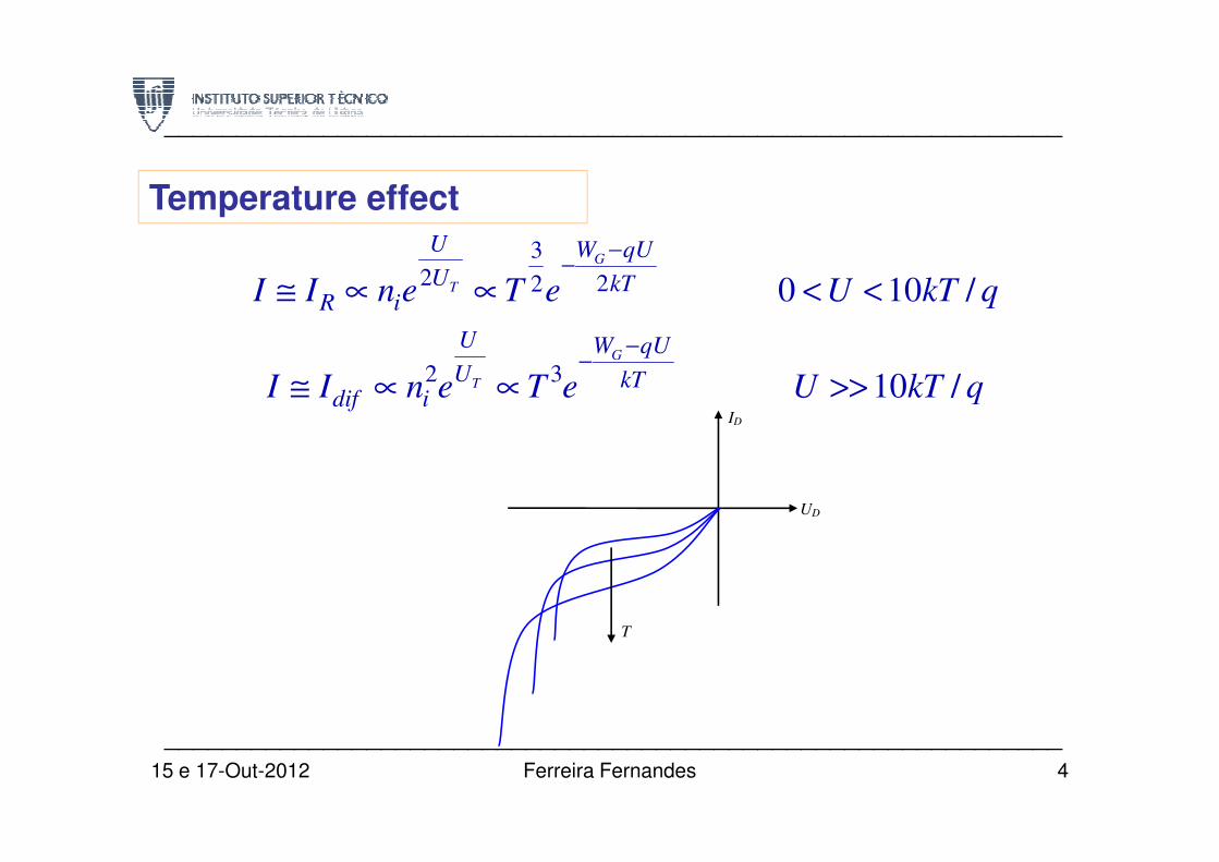
Temperature effect
3
2 22 0 10 /
G
T
U W qU
U kTR iI I n e T e U kT q
−−
≅ ∝ ∝ < <
2 310 /
G
T
U W qU
U kTdif iI I n e T e U kT q
−−
≅ ∝ ∝ >> ID
15 e 17-Out-2012 Ferreira Fernandes 4
______________________________________________________________
UD
T
______________________________________________________________
( )( )
1
20
2
A DT C
A D
qN NC A V
N NU
−ε= −
+
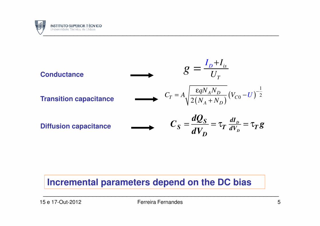
Conductance
is
T
D II
Ug
+=
Transition capacitance
dQ
15 e 17-Out-2012 Ferreira Fernandes 5
______________________________________________________________
= = τ = τD
D
dISS T TdV
D
dQC g
dVDiffusion capacitance
Incremental parameters depend on the DC bias
______________________________________________________________
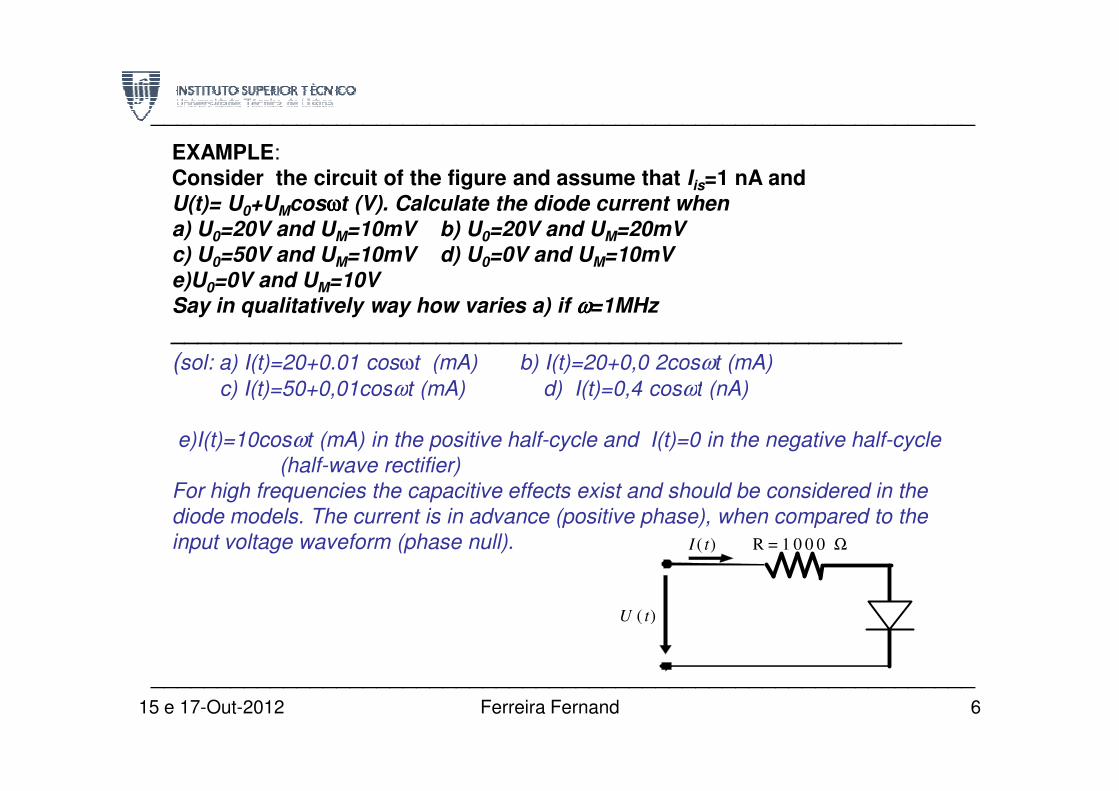
EXAMPLE:
Consider the circuit of the figure and assume that Iis=1 nA andU(t)= U0+UMcosωωωωt (V). Calculate the diode current when
a) U0=20V and UM=10mV b) U0=20V and UM=20mV
c) U0=50V and UM=10mV d) U0=0V and UM=10mV
e)U0=0V and UM=10V
Say in qualitatively way how varies a) if ωωωω=1MHz
_______________________________________________________(sol: a) I(t)=20+0.01 cosωt (mA) b) I(t)=20+0,0 2cosωt (mA)
c) I(t)=50+0,01cosωt (mA) d) I(t)=0,4 cosωt (nA)
15 e 17-Out-2012 Ferreira Fernandes 6
c) I(t)=50+0,01cosωt (mA) d) I(t)=0,4 cosωt (nA)
e)I(t)=10cosωt (mA) in the positive half-cycle and I(t)=0 in the negative half-cycle
(half-wave rectifier)
For high frequencies the capacitive effects exist and should be considered in the
diode models. The current is in advance (positive phase), when compared to the
input voltage waveform (phase null). I ( t) R = 1 0 0 0 Ω
U ( t)
______________________________________________________________
______________________________________________________________
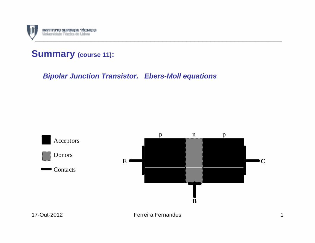
Summary (course 11):
Bipolar Junction Transistor Ebers Moll equationsBipolar Junction Transistor. Ebers-Moll equations
p n p
E C
p pAcceptors Donors CContacts
17-Out-2012 Ferreira Fernandes 1
B
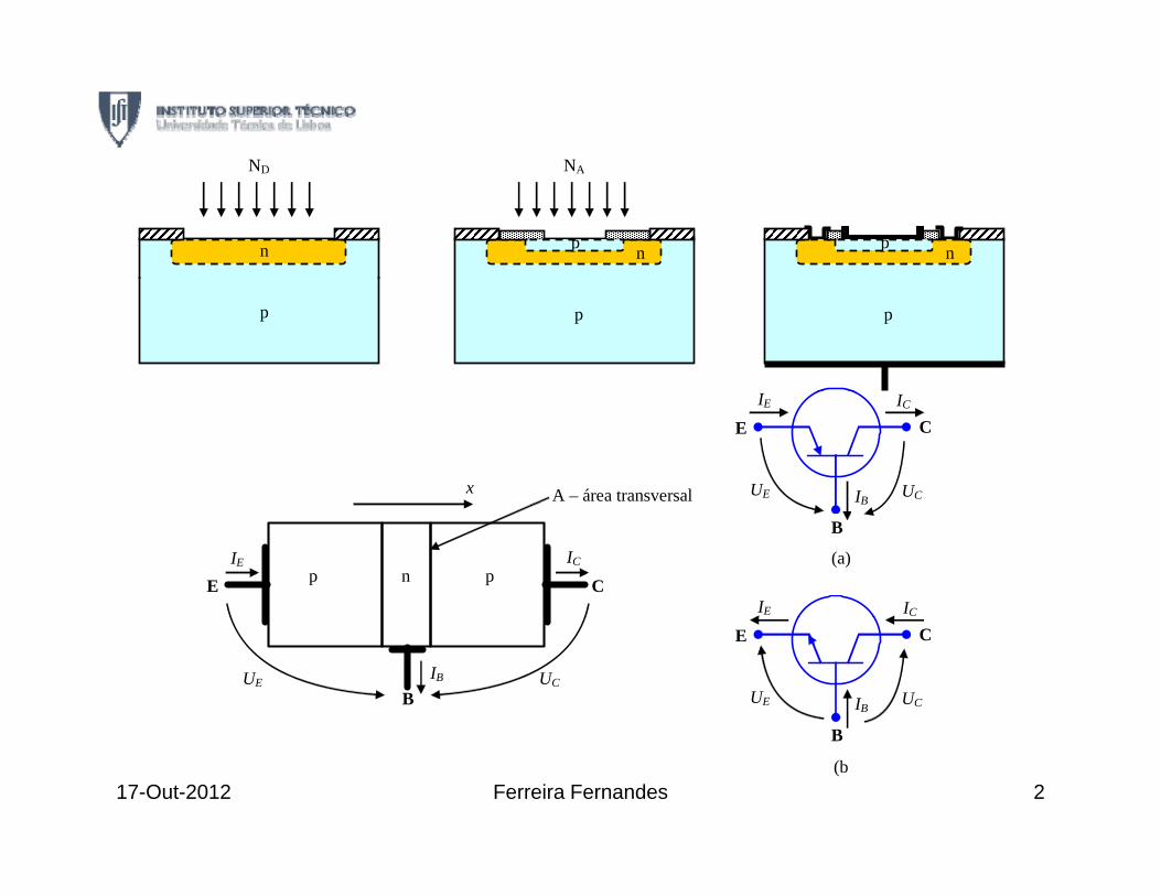
ND NA ND
n
NA
np np
p
p
p
A – área transversal x
IE IC
IB
E C
UCUE
E C p n p IE IC
B
IE IC
(a)
B IB UE UC
IB
E
B
C
UCUE
17-Out-2012 Ferreira Fernandes 2
B
(b
______________________________________________________________
Conventions adopted in this course that are common to p-n-pand to n-p-n
1. In the symbol the arrow is in emitter terminal directed from p to n asin a diode;
2. Reference for voltages: Theses are referenced from p-side to n-sideof the colector-base and emitter-base junctions. Therefore they arepositive (negative) for forward (reversed)-biased;
3. Rference for currents: The emitter current is taken with the directionof the arrow. If it enters (leaves) the other two leave (enter) theof the arrow. If it enters (leaves) the other two leave (enter) thetransistor. Therefore we can assume that the KCL is given byIE=IB+IC;
4. Dissipated power is important in the active zone. In cut zoneti ll th t i th t ti th ltpractically there are no currents; in the saturation zone the voltages
are negligible;5. In the active zone the emitted power in the transistor is practically
the power in the collector junction and it is given by –(Uc.Ic).
17-Out-2012 Ferreira Fernandes 3______________________________________________________________
p j g y ( )
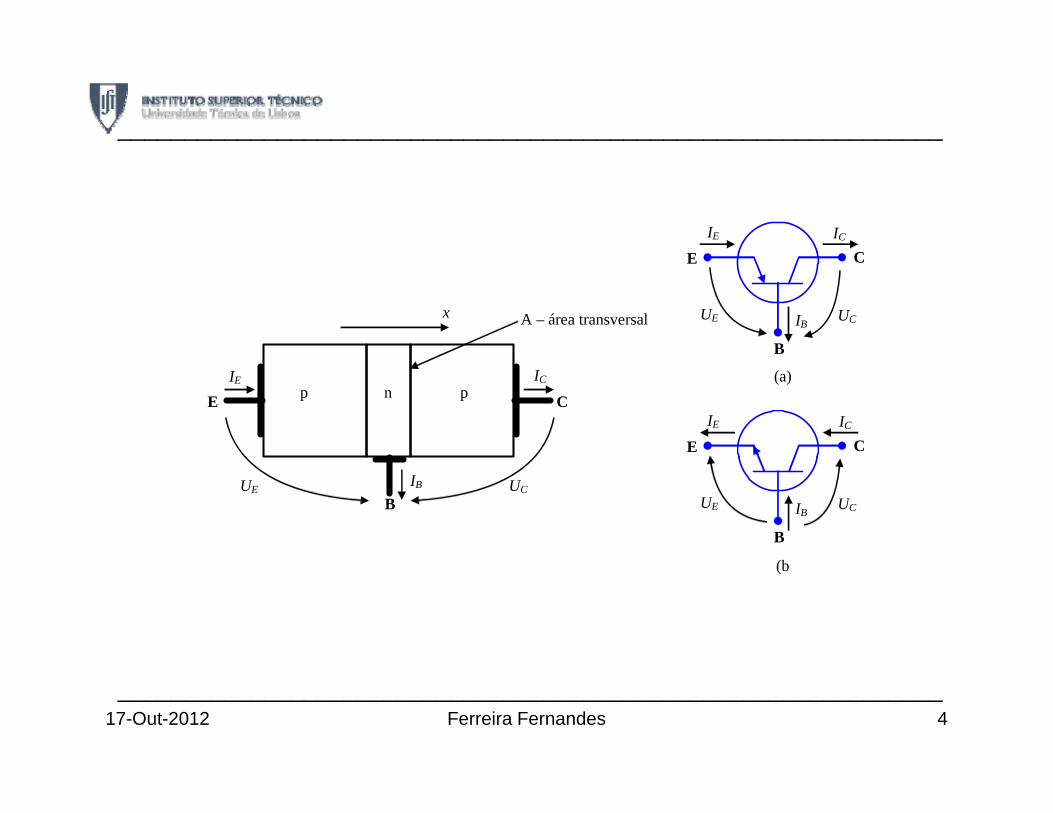
______________________________________________________________
IE IC E C
A – área transversal x IB
E
B
C
UCUE
E C p n p IE IC
IE IC E C
(a)
B IB UE UC
IB
B
UCUE
(b(b
17-Out-2012 Ferreira Fernandes 4______________________________________________________________

What is represented in the Figure?
17-Out-2012 Ferreira Fernandes 5

And now?
17-Out-2012 Ferreira Fernandes 6

Now, I think noone doubts…
17-Out-2012 Ferreira Fernandes 7
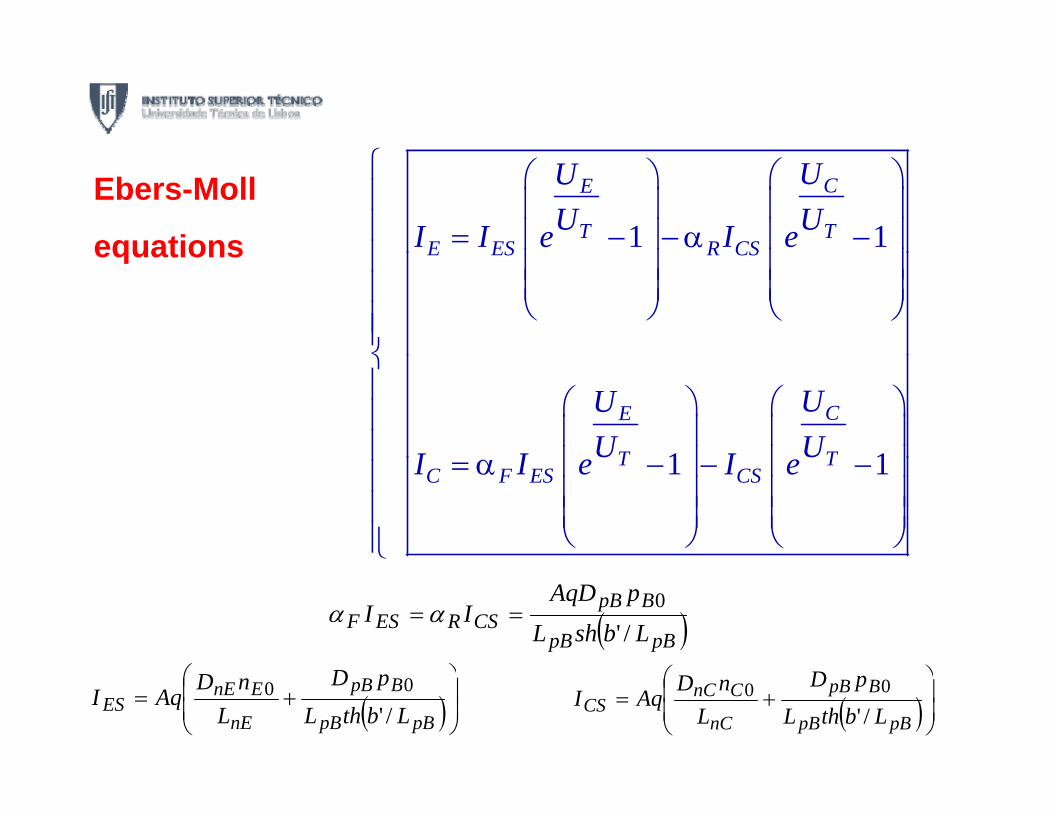
⎧
1 1
CE
T TE ES R CS
UUU UI I e I e
⎧ ⎛ ⎞⎛ ⎞⎪ ⎜ ⎟⎜ ⎟⎪ ⎜ ⎟⎜ ⎟= − −α −⎪ ⎜ ⎟⎜ ⎟
Ebers-Moll
equations E ES R CS⎪ ⎜ ⎟⎜ ⎟⎜ ⎟ ⎜ ⎟⎪ ⎝ ⎠ ⎝ ⎠⎪⎪
⎨
equations
1 1
CE
T T
UUU UI I I
⎨⎪ ⎛ ⎞⎛ ⎞⎪ ⎜ ⎟⎜ ⎟⎪ ⎜ ⎟⎜ ⎟1 1T T
C F ES CSI I e I e⎪ ⎜ ⎟⎜ ⎟= α − − −⎪ ⎜ ⎟⎜ ⎟⎪ ⎜ ⎟ ⎜ ⎟⎝ ⎠ ⎝ ⎠⎪⎩
( )pBpB
BpBCSRESF LbshL
pAqDII
/'0== αα
⎞⎛
( )⎟⎟⎠⎞
⎜⎜⎝
⎛+=
pBpB
BpB
nE
EnEES LbthL
pDL
nDAqI
/'00
( )⎟⎟⎠⎞
⎜⎜⎝
⎛+=
pBpB
BpB
nC
CnCCS LbthL
pDL
nDAqI
/'00
______________________________________________________________
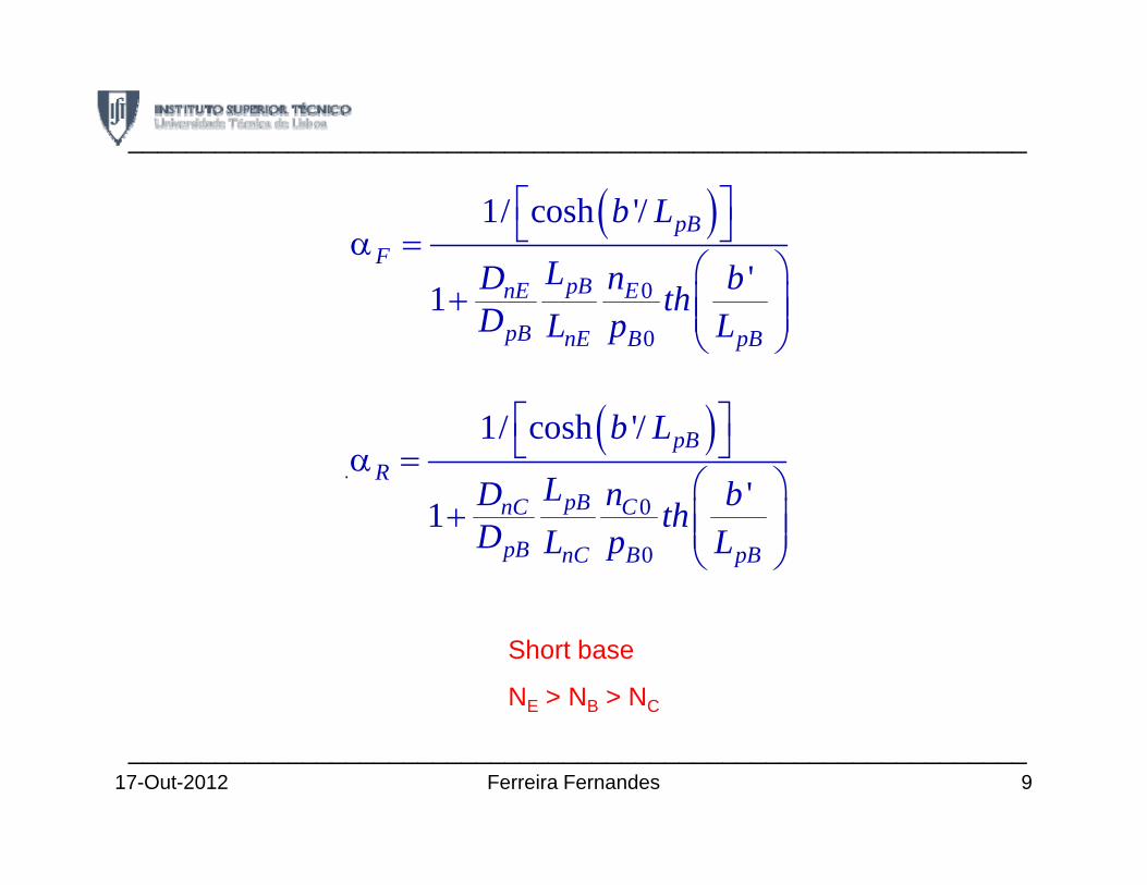
( )1/ cosh '/
'
pBF
b L
LD n b
⎡ ⎤⎣ ⎦α =
⎛ ⎞0
0
'1 pBnE E
pB nE B pB
LD n bthD L p L⎛ ⎞
+ ⎜ ⎟⎜ ⎟⎝ ⎠
.
( )1/ cosh '/
'
pBR
B
b L
LD n b
⎡ ⎤⎣ ⎦α =
⎛ ⎞⎜ ⎟0
01 pBnC C
pB nC B pB
LD n bthD L p L⎛ ⎞
+ ⎜ ⎟⎜ ⎟⎝ ⎠
Short base
NE > NB > NC
9Ferreira Fernandes______________________________________________________________
17-Out-2012
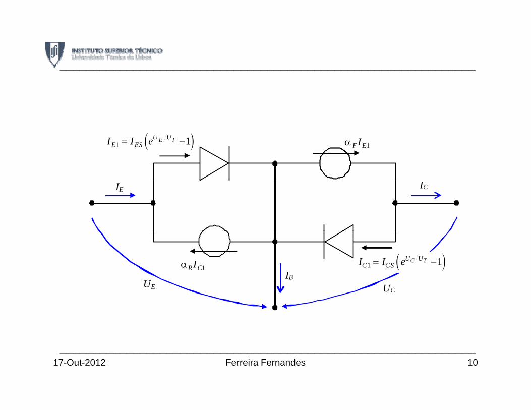
______________________________________________________________
( )1 1E TU UE ESI I e= − 1F EIα
IE IC
1R CIαIB
U
( )1 1C TU UC CSI I e= −
UCUE
10Ferreira Fernandes______________________________________________________________
17-Out-2012
______________________________________________________________
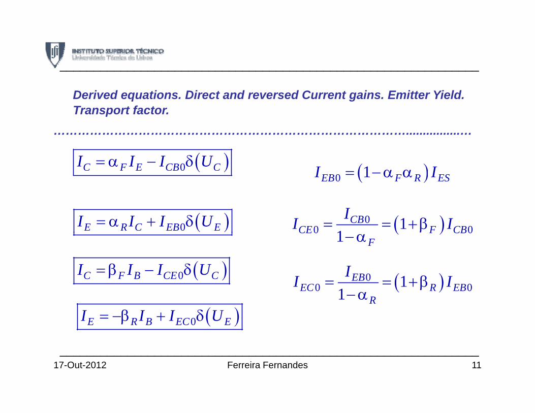
Derived equations. Direct and reversed Current gains. Emitter Yield. Transport factor.
……………………………………………………………………………................…
( )0C F E CB CI I I U= α − δ ( )0 1EB F R ESI I= −α α
( )0E R C EB EI I I U= α + δ
( )0EB F R ES
( )00 01
1CB
CE F CBII I= = +β
( )0C F B CE CI I I U= β − δ
( )0 01CE F CBF−α
( )00 01EB
EC R EBII I= = +β
( )0E R B EC EI I I U= −β + δ
( )0 011EC R EB
RI I+β
−α
11Ferreira Fernandes______________________________________________________________
17-Out-2012
______________________________________________________________
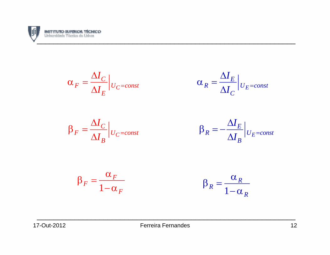
CIΔ EIΔC
CF U const
EI =α =Δ E
ER U const
CI =α =Δ
CC
F U constB
II =
Δβ =
Δ EE
R U constB
II =
Δβ = −
Δ
Fα α1
FF
F
αβ =
−α 1R
RR
αβ =
−α
12Ferreira Fernandes______________________________________________________________
17-Out-2012
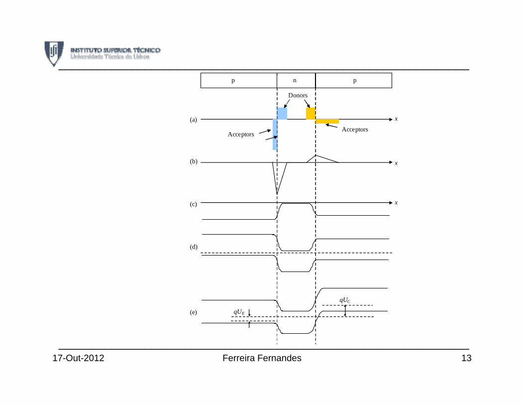
______________________________________________________________p n p
(a)
Donors
x
Acceptors Acceptors
x (b)
x (c)
(d)
(e)
qUC
qUE
13Ferreira Fernandes______________________________________________________________
17-Out-2012
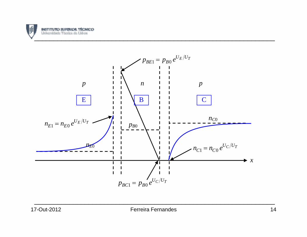
______________________________________________________________
1 0
E TU UBE Bp p e=
p n p
E B C
nC0 1 0
E TU UE En n e= pB0
nE0
x1 0
C TU UC Cn n e=
1 0C TU U
BC Bp p e=
14Ferreira Fernandes______________________________________________________________
17-Out-2012
______________________________________________________________
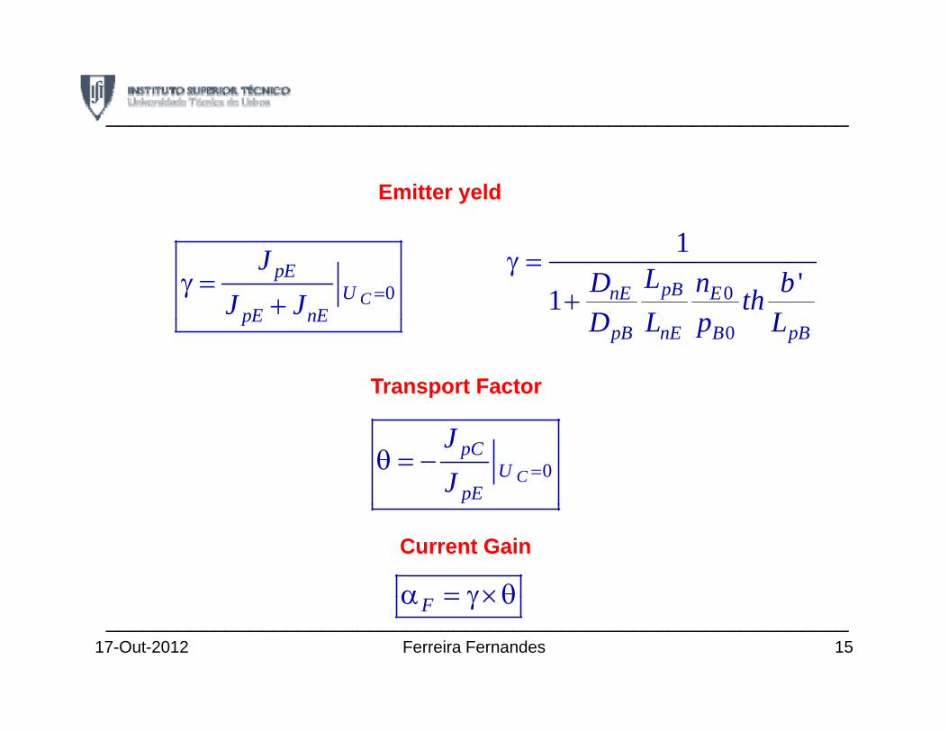
Emitter yeld
0CpE
UpE nE
JJ J =γ =
+ 0
1'1 pBnE ELD n bth
D L p L
γ =+pE nE
0pB nE B pBD L p L
Transport Factor
0CpC
UpE
JJ =θ = −
α = γ×θ
Current Gain
Fα = γ×θ
15Ferreira Fernandes______________________________________________________________
17-Out-2012
______________________________________________________________
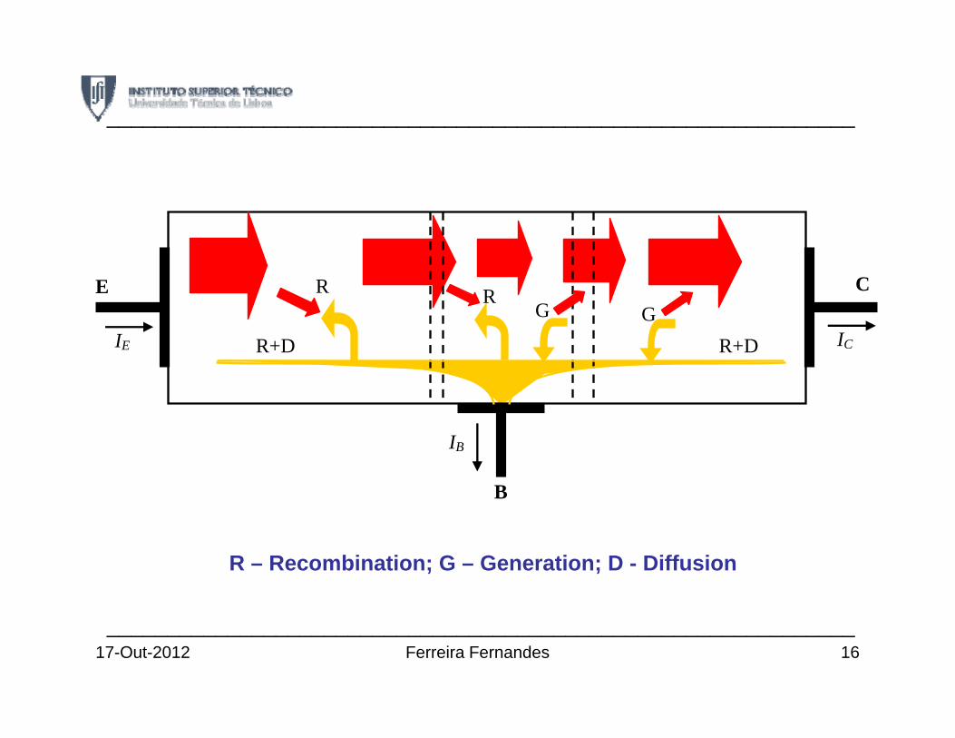
E C R R G G
IE IC R+D R+D
B
IB
R – Recombination; G – Generation; D - Diffusion
16Ferreira Fernandes______________________________________________________________
17-Out-2012
______________________________________________________________
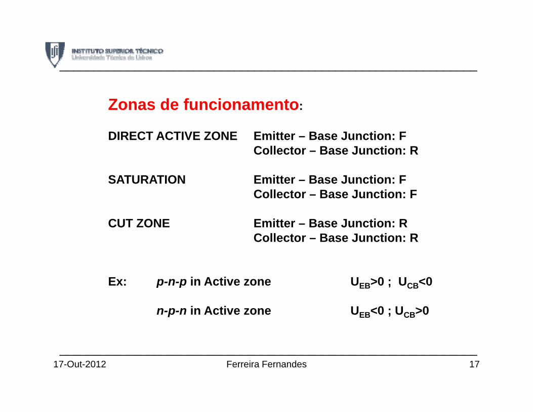
Zonas de funcionamento:
DIRECT ACTIVE ZONE Emitter – Base Junction: FCollector – Base Junction: R
SATURATION Emitter – Base Junction: FSATURATION Emitter – Base Junction: FCollector – Base Junction: F
CUT ZONE Emitter – Base Junction: RCollector – Base Junction: R
Ex: p-n-p in Active zone UEB>0 ; UCB<0Ex: p n p in Active zone UEB>0 ; UCB<0
n-p-n in Active zone UEB<0 ; UCB>0
17-Out-2012 Ferreira Fernandes 17______________________________________________________________
______________________________________________________________
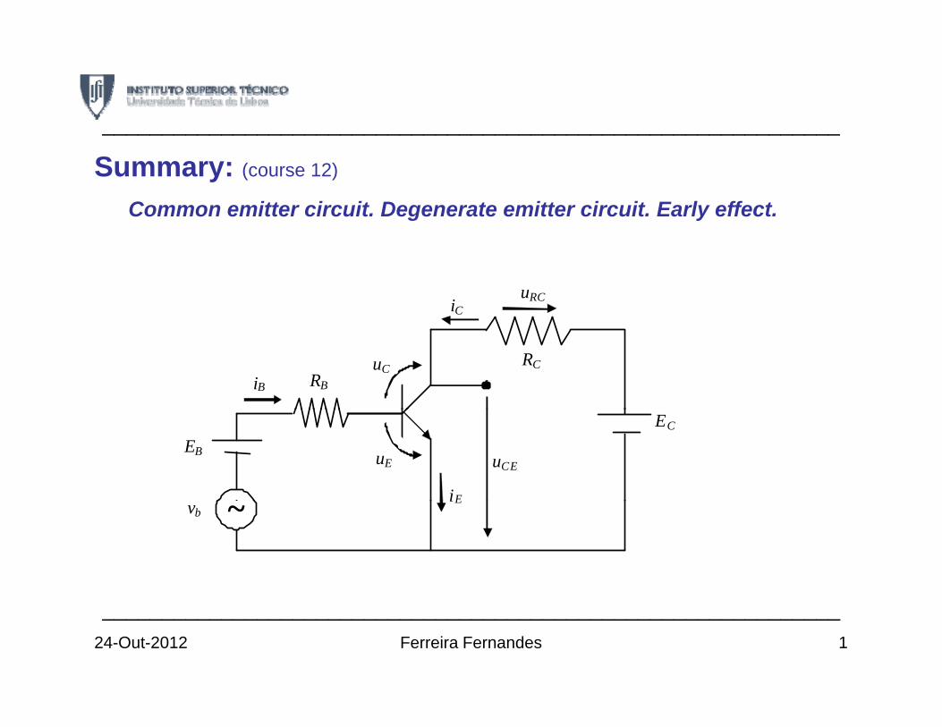
Summary: (course 12)
Common emitter circuit. Degenerate emitter circuit. Early effect.
______________________________________________________________
iC
uRC
iB RBuC RC
EB uE
iE
uCE
EC
iE~ vb
24-Out-2012 Ferreira Fernandes 1
______________________________________________________________
______________________________________________________________
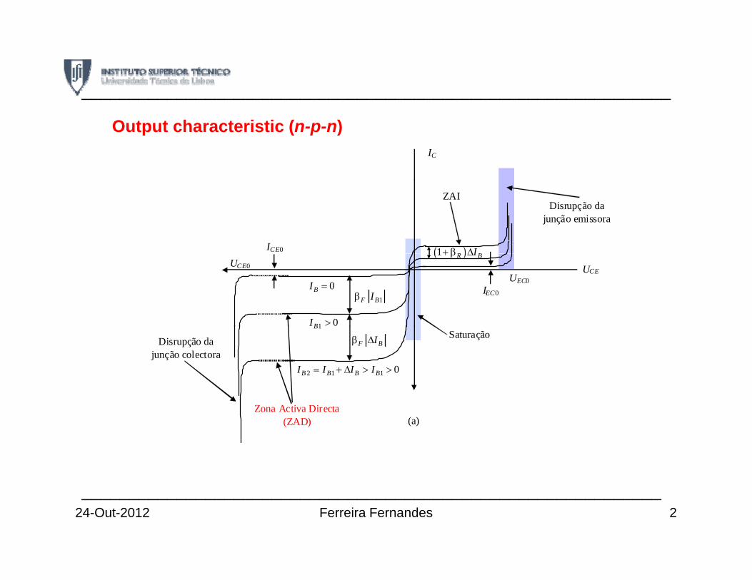
IC
Output characteristic (n-p-n)
( )1 R BI+ β ΔICE0
ZAI Disrupção da
junção emissora
( )1 R BI+ β Δ
UCE 0BI =
1 0BI >
1F BIβ
UEC0
UCE0
IEC0
1B
2 1 1 0B B B BI I I I= + Δ > >
F BIβ ΔDisrupção da junção colectora
Saturação
Zona Activa Directa (ZAD) (a)
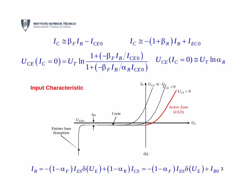
_____________________________________________________________2Ferreira Fernandes24-Out-2012
0C F B CEI I I≅ β − ( ) 01C R B ECI I I≅ − +β +
( ) ( )010 l F B CEI I
U I U+ −β ( 0) lnU I U= ≅ α
I U U
( ) ( )( )
0
00 ln
1F B CE
CE C TF B R CE
U I UI I
β= =
+ −β α( 0) lnCE C T RU I U= ≅ α
Input Characteristic IB CE TU U−
0CEU =0CEU >
Active Zone
UEdisr.
IB0
Emitter base di ti
UE
Active Zone (ZAD) Corte
disruption
(b) ( )
( ) ( ) ( ) ( ) ( ) 01 1 1B F ES E R CS F ES E BI I U I I U I= − −α δ + −α = − −α δ + 3
______________________________________________________________
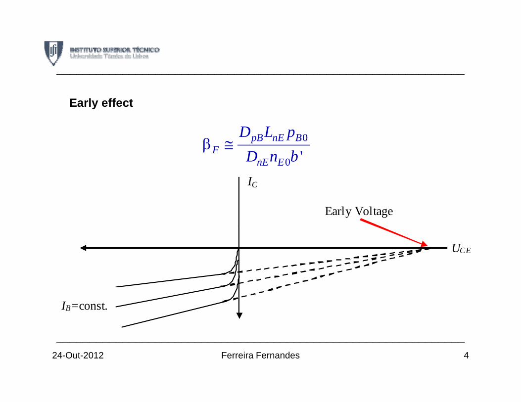
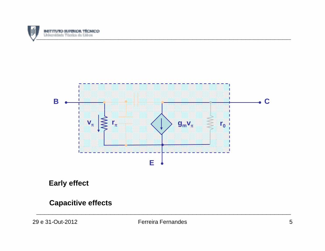
Early effect
______________________________________________________________
0
0 'pB nE B
FnE E
D L pD n b
β ≅
IC
Early Voltage
UCE
IB=const.
Ferreira Fernandes 424-Out-2012
______________________________________________________________
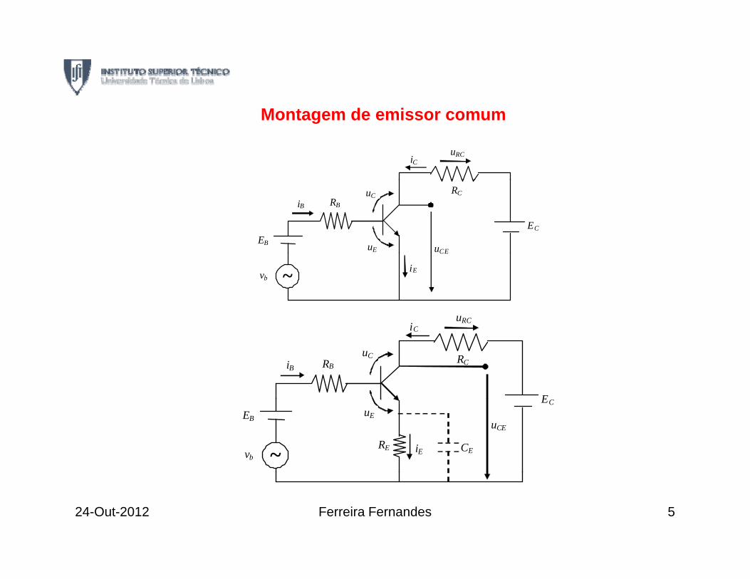
iC
uRC
Montagem de emissor comum
iB
EB
RBuC
uE uCE
EC
RC
iE
CE
~vb
i
uRC
iB RBuC
iC
E
RC
EB uE
iE
uCE
EC
~vbRE CE
Ferreira Fernandes 524-Out-2012
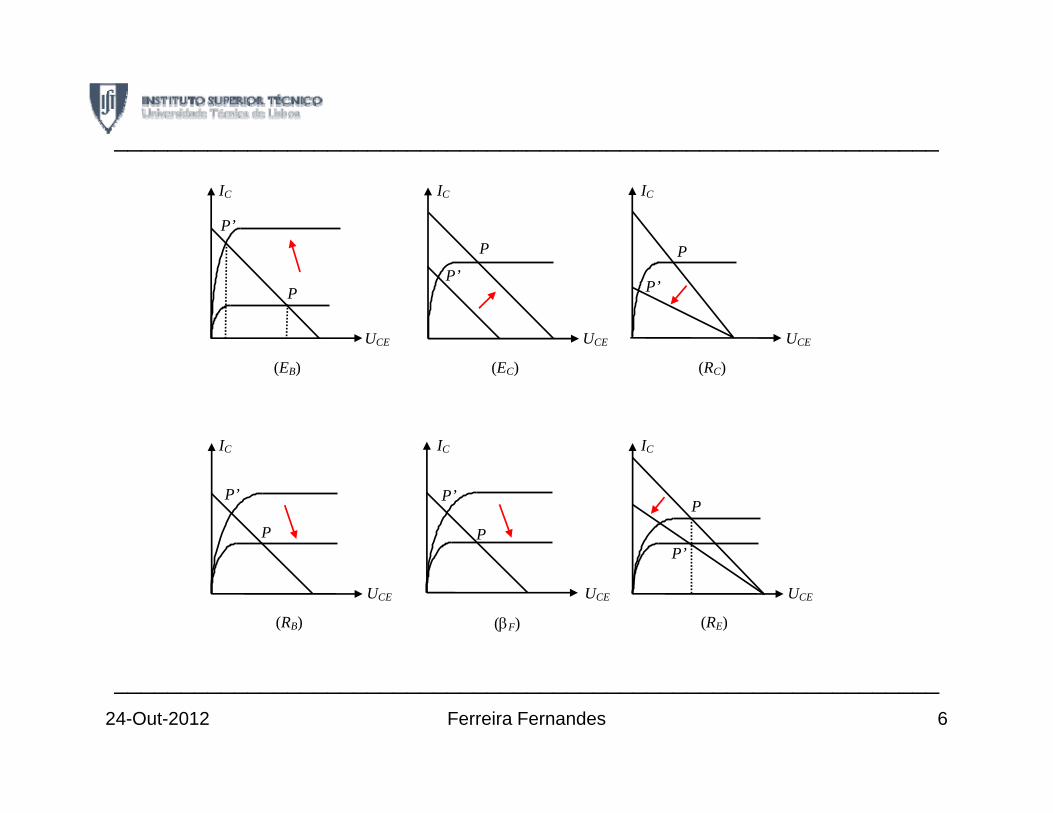
______________________________________________________________
IC
P’
IC
P
IC
P
______________________________________________________________
P
UCE
P
UCE
P’ P
UCE
P’
(EB) (EC) (RC)
IC IC IC
P
P’
P
P’ P
P’
UCE
(RB)
UCE
(βF)
UCE
(RE)
Ferreira Fernandes 624-Out-2012
______________________________________________________________
______________________________________________________________
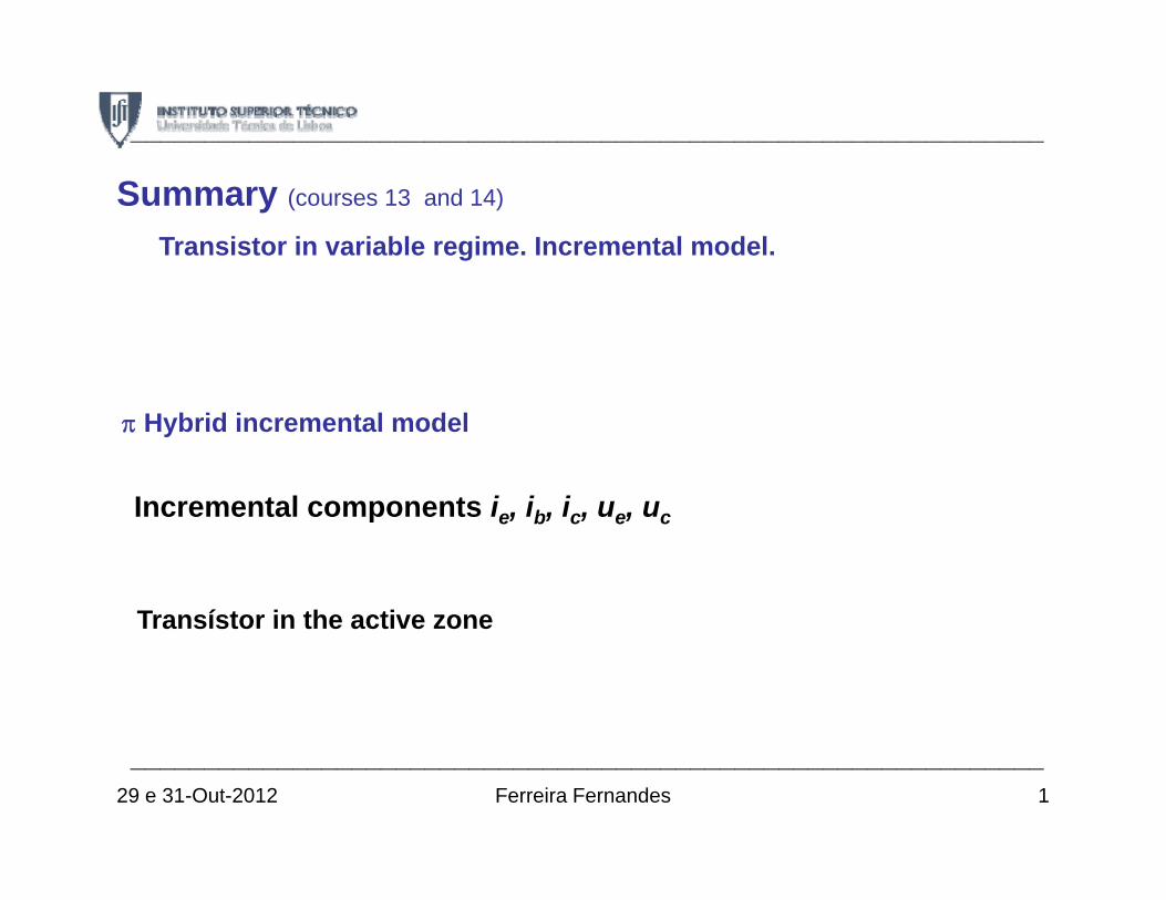
Summary (courses 13 and 14)
Transistor in variable regime. Incremental model.
π Hybrid incremental model
Incremental components i i i u uIncremental components ie, ib, ic, ue, uc
Transístor in the active zoneTransístor in the active zone
29 e 31-Out-2012 Ferreira Fernandes 1
______________________________________________________________
______________________________________________________________
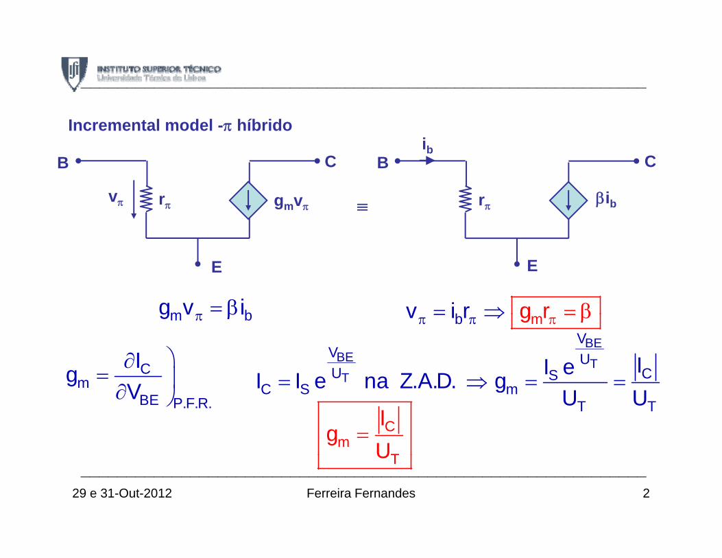
Incremental model -π híbrido
B Cib
B C
vπ rπ gmvπ ≡ rπ βib
E E
π = βm bg v i = ⇒ = βb gr rv iπ βm bg v iπ π π= ⇒ = βmb gr rv i
⎞∂= ⎟∂ ⎠
Cm
IgV = ⇒ = =
BEBE TT
VV UU CS
C SII eI I e na Z A D g⎟∂ ⎠
mBE P.F.R.
gV = ⇒ = =C S m
T TI I e na Z.A.D. g
U U= C
mT
Ig
UTU______________________________________________________________
2Ferreira Fernandes29 e 31-Out-2012
______________________________________________________________
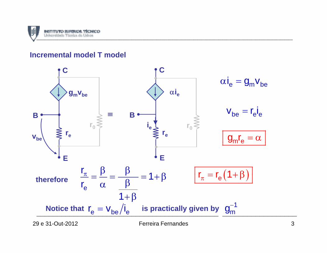
Incremental model T model
C Ci g
gmvbe αieα =e m bei g v
=v r iB
re
≡ B
re
ie
=be e ev r i
= αm eg rvbe
r0 r0
E E
m eg
π β ββ
r 1 ( )= + βr r 1thereforeπ β β= = = + β
βα+ β
e1
r1
( )π = + βer r 1
N ti th t i ti ll i br i −1gNotice that is practically given by=e be er v i 1mg____________________________________________ __________________
3Ferreira Fernandes29 e 31-Out-2012
______________________________________________________________
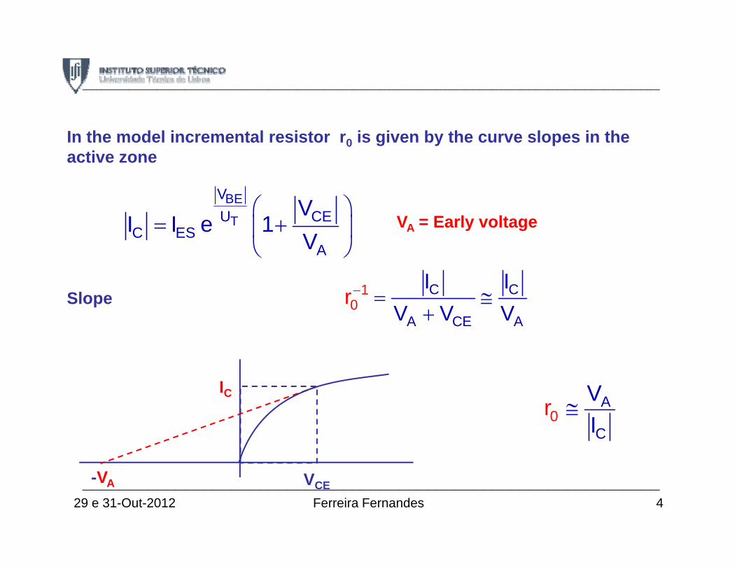
In the model incremental resistor r0 is given by the curve slopes in the active zone
⎛ ⎞= +⎜ ⎟
⎝ ⎠
BE
T
VU CE
C ESA
VI I e 1
VVA = Early voltage
⎝ ⎠AV
Slope − = ≅+C C
A C
10
E AVr
I IV VA CE A
VIC≅ A
0C
r VI
IC
VCE-VA______________________________________________________________4Ferreira Fernandes29 e 31-Out-2012
______________________________________________________________
B C
rπ gmvπ r0vπ
E
Early effect
Capacitive effectsCapacitive effects______________________________________________________________
5Ferreira Fernandes29 e 31-Out-2012
______________________________________________________________
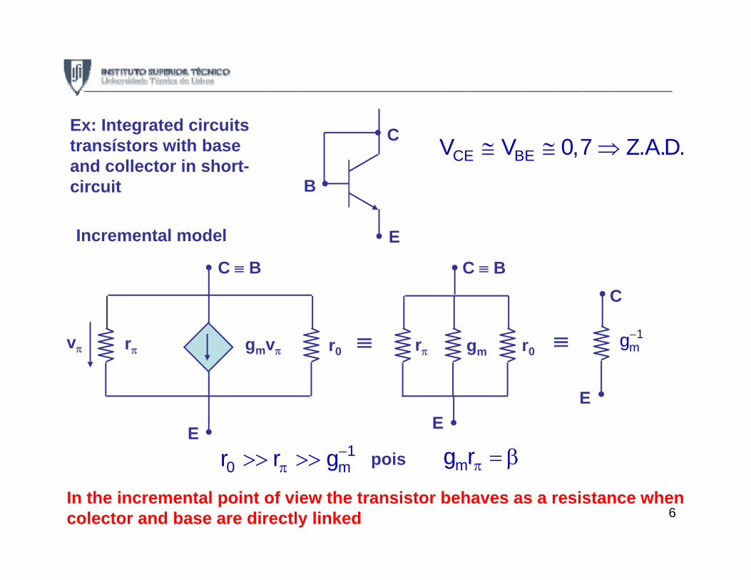
Ex: Integrated circuits transístors with base and collector in short-
i it B
C≅ ≅ ⇒CE BEV V 0,7 Z.A.D.
circuit B
EIncremental model
C ≡ B C ≡ BC
rπ gmvπ r0vπ ≡ rπ gm r0 ≡
E
−1mg
E EE
−π>> >> 1
0 mr r g pois π = βmg r
In the incremental point of view the transistor behaves as a resistance when colector and base are directly linked 6
______________________________________________________________
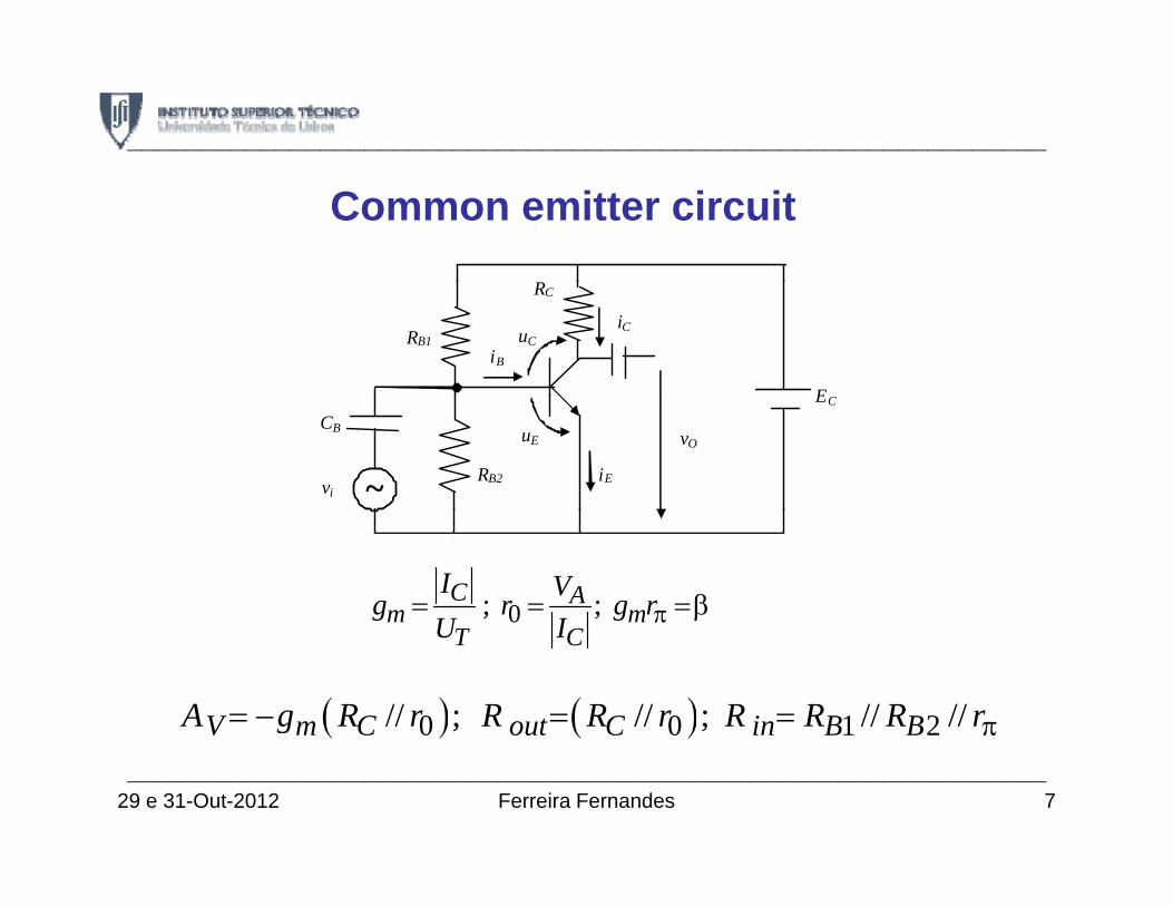
Common emitter circuit
RC
iB RB1 uC
iC
ECB
uE
iE
vO
RB2
EC
~ vi
0; ;C Am m
I Vg r g rU I π= = =β
T CU I
( ) ( )0 0 1 2// ; // ; // //V m C out C in B BA g R r R R r R R R rπ= − = =
29 e 31-Out-2012 Ferreira Fernandes 7______________________________________________________________
C itt i it______________________________________________________________
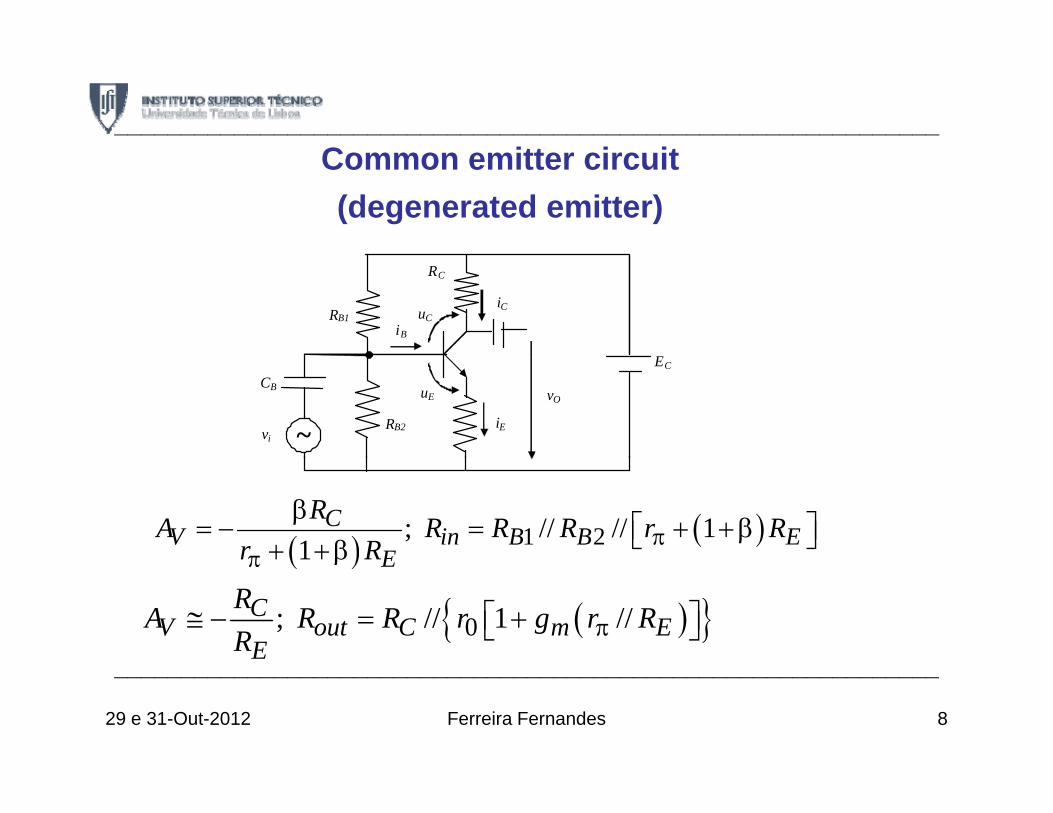
Common emitter circuit (degenerated emitter)
RC
iB RB1 uC
iC
CB uE
iE
vO
RB2
EC
~ vi
( ) ( )1 2; // // 11
CV in B B E
E
RA R R R r Rr R ππ
β= − = + +β⎡ ⎤⎣ ⎦+ +β( ) Eπ β
( ) 0; // 1 //CV out C m E
E
RA R R r g r RR π⎡ ⎤≅ − = +⎣ ⎦
29 e 31-Out-2012 Ferreira Fernandes 8
______________________________________________________________
______________________________________________________________
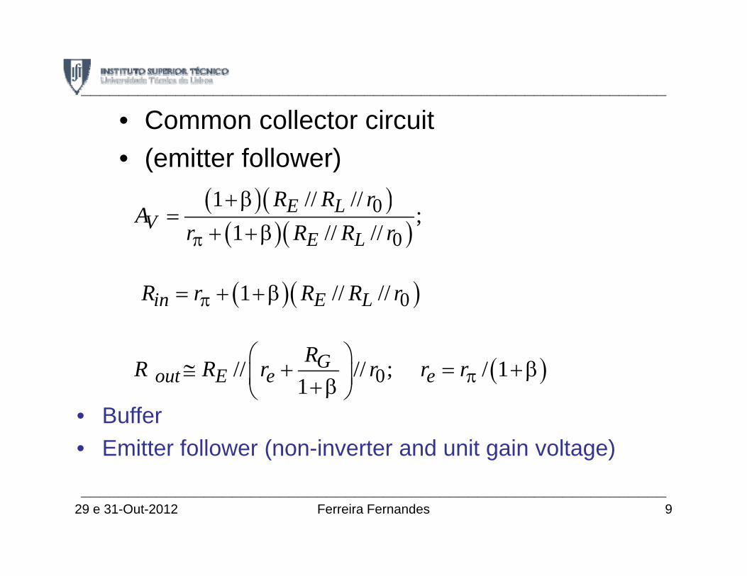
• Common collector circuit• (emitter follower)
( )( )( )( )
0
0
1 // //;
1 // //E L
VE L
R R rA
r R R rπ
+β=
+ +β
( )( )01 // //in E LR r R R rπ= + +β
( )0// // ; / 11
Gout E e e
RR R r r r rπ⎛ ⎞
≅ + = +β⎜ ⎟+β⎝ ⎠β⎝ ⎠• Buffer• Emitter follower (non-inverter and unit gain voltage)
29 e 31-Out-2012 Ferreira Fernandes 9______________________________________________________________
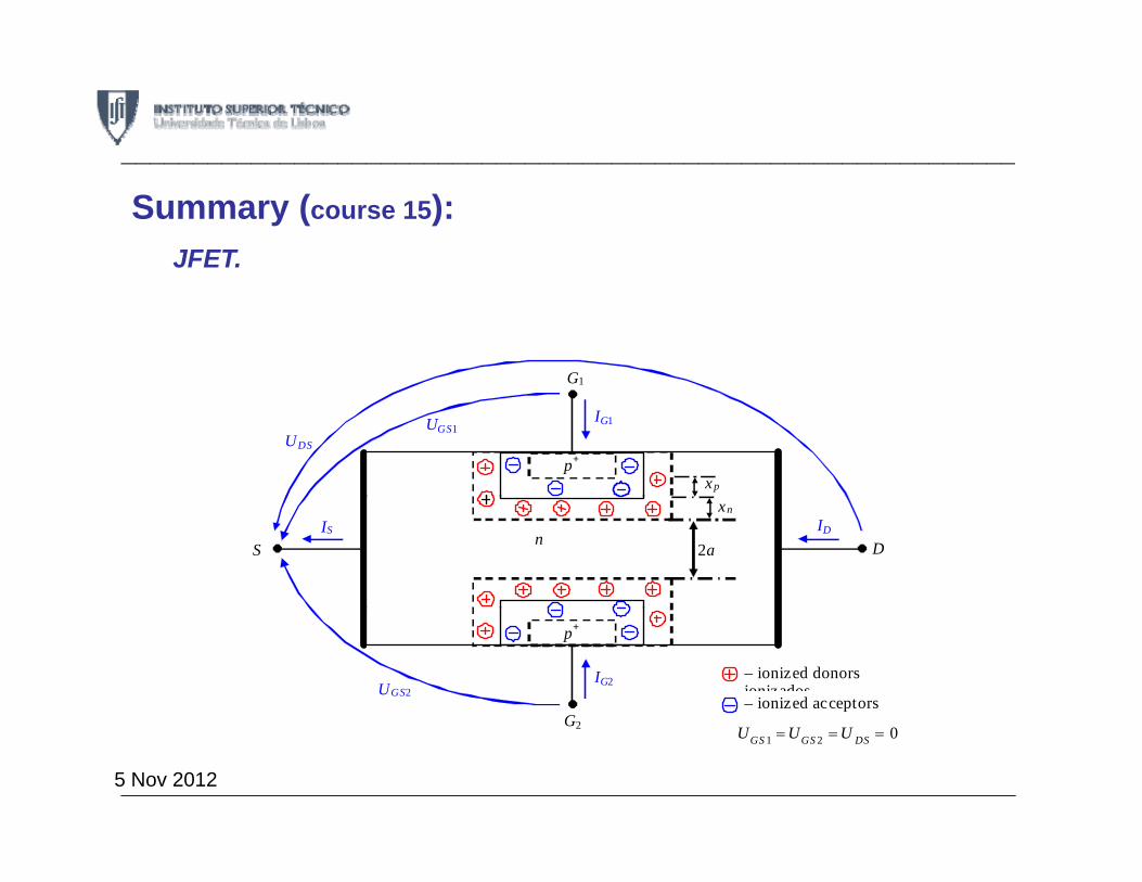
Summary (course 15):JFET.
______________________________________________________________
G1
UDS UGS1
IG1
xp p+
ID IS D S
n 2a
xn
UGS2 IG2
G
– ionized donors ionizados– ionized acceptors
p+
G21 2 0= = =GS GS DSU U U
______________________________________________________________5 Nov 2012

______________________________________________________________
UDS IG
G
ID IS D S
n
y
L
a xn (y)
( )02 1
=+
c An
D A D
V Nxq N N Nεx
y
V1V2 J
V = const. xn(y)
V3 V4
Vn . . .
( )( )
02 1−=
+c GSP A
D A D
V U Naq N N N
ε
x
V1
J
x
______________________________________________________________5 Nov 2012
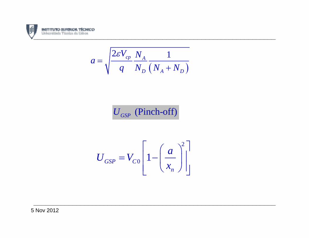
______________________________________________________________
( )2 1
=+
cp A
D A D
V Naq N N Nε
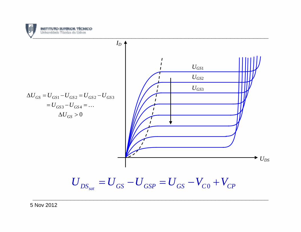
(Pinch-off)GSPU
2
0 1⎡ ⎤⎛ ⎞⎢ ⎥= − ⎜ ⎟⎢ ⎥⎝ ⎠
GSP CaU V
⎢ ⎥⎝ ⎠⎣ ⎦nx
______________________________________________________________5 Nov 2012
______________________________________________________________
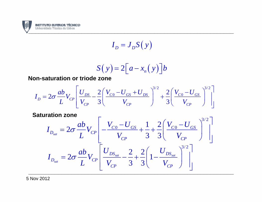
( )D DI J S y=
( ) ( )2 nS y a x y b= −⎡ ⎤⎣ ⎦
3/ 2 3/ 2⎡ ⎤⎛ ⎞ ⎛ ⎞
Non-saturation or triode zone3/ 2 3/ 2
0 02 223 3
DS C GS DS C GSD CP
CP CP CP
U V U U V UabI VL V V V
⎡ ⎤⎛ ⎞ ⎛ ⎞− + −⎢ ⎥= − +⎜ ⎟ ⎜ ⎟⎢ ⎥⎝ ⎠ ⎝ ⎠⎣ ⎦
σ
S t ti3/ 2
0 01 223 3sat
C GS C GSD CP
CP CP
ab V U V UI VL V V
⎡ ⎤⎛ ⎞− −⎢ ⎥= − + + ⎜ ⎟⎢ ⎥⎝ ⎠⎣ ⎦
σ
Saturation zone
CP CP⎢ ⎥⎝ ⎠⎣ ⎦3/ 2
2 22 13 3
sat sat
sat
DS DSD CP
CP CP
U UabI VL V V
⎡ ⎤⎛ ⎞⎢ ⎥= − + −⎜ ⎟⎢ ⎥⎝ ⎠⎣ ⎦
σ3 3CP CPL V V⎢ ⎥⎝ ⎠⎣ ⎦______________________________________________________________
5 Nov 2012
I______________________________________________________________
ID
UGS1 UGS2
UGS3 1 2 2 3Δ = − = −GS GS GS GS GSU U U U U
3 4
0= − =
Δ >
…GS GS
GS
U UU
UDSUDS
0= − = − +satDS GS GSP GS C CPU U U U V Vsat
______________________________________________________________5 Nov 2012
______________________________________________________________
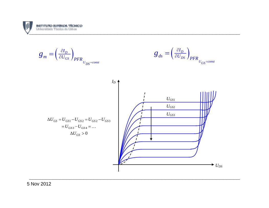
( )=
∂∂= D
GSU constDS
Im U PFR
g ( )=
∂∂= D
DSU constGS
Ids U PFR
gDS
ID
UGS1 UGS2
UGS3 1 2 2 3
3 4
0
Δ = − = −
= − =
Δ >
…GS GS GS GS GS
GS GS
GS
U U U U UU U
U
UDS
______________________________________________________________5 Nov 2012
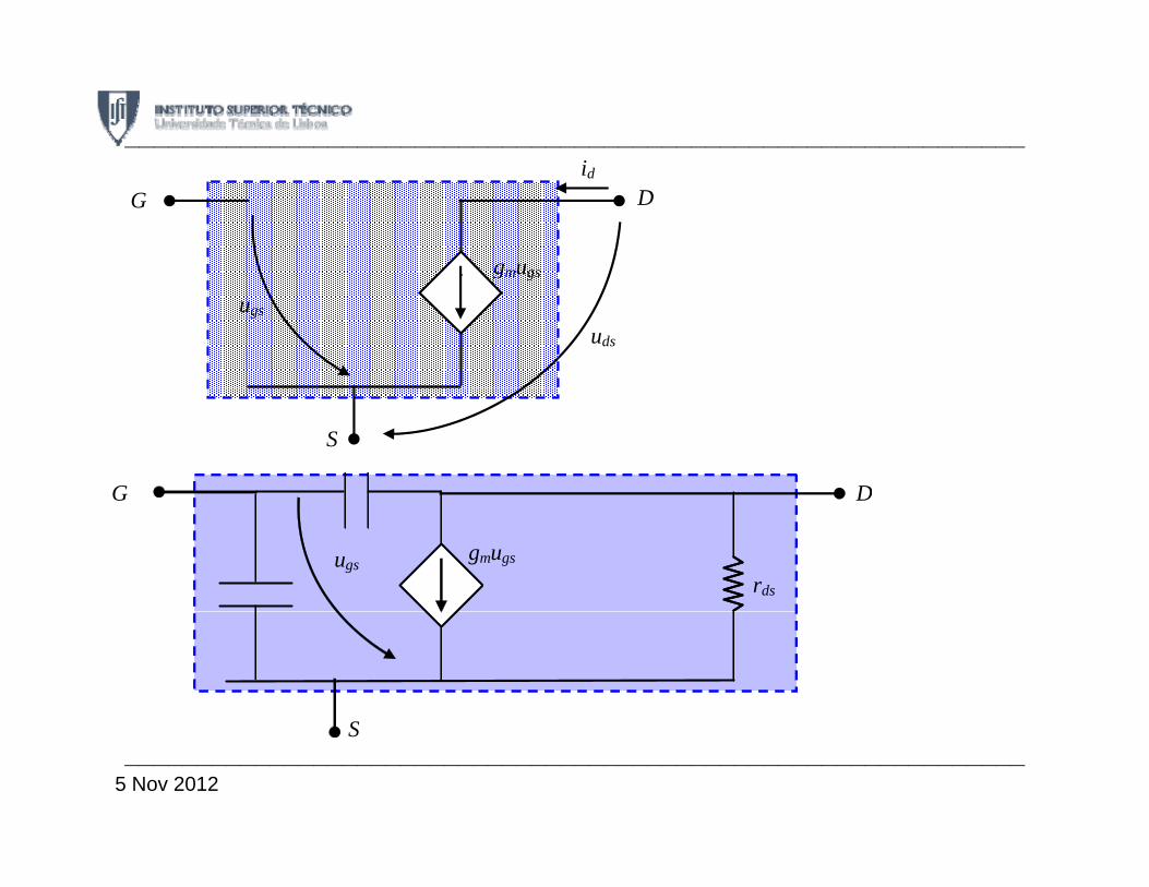
i______________________________________________________________
id
D G
gmugs
ugs uds
gm gs
S
DG
rds
DG
ugs gmugs
SS______________________________________________________________
5 Nov 2012
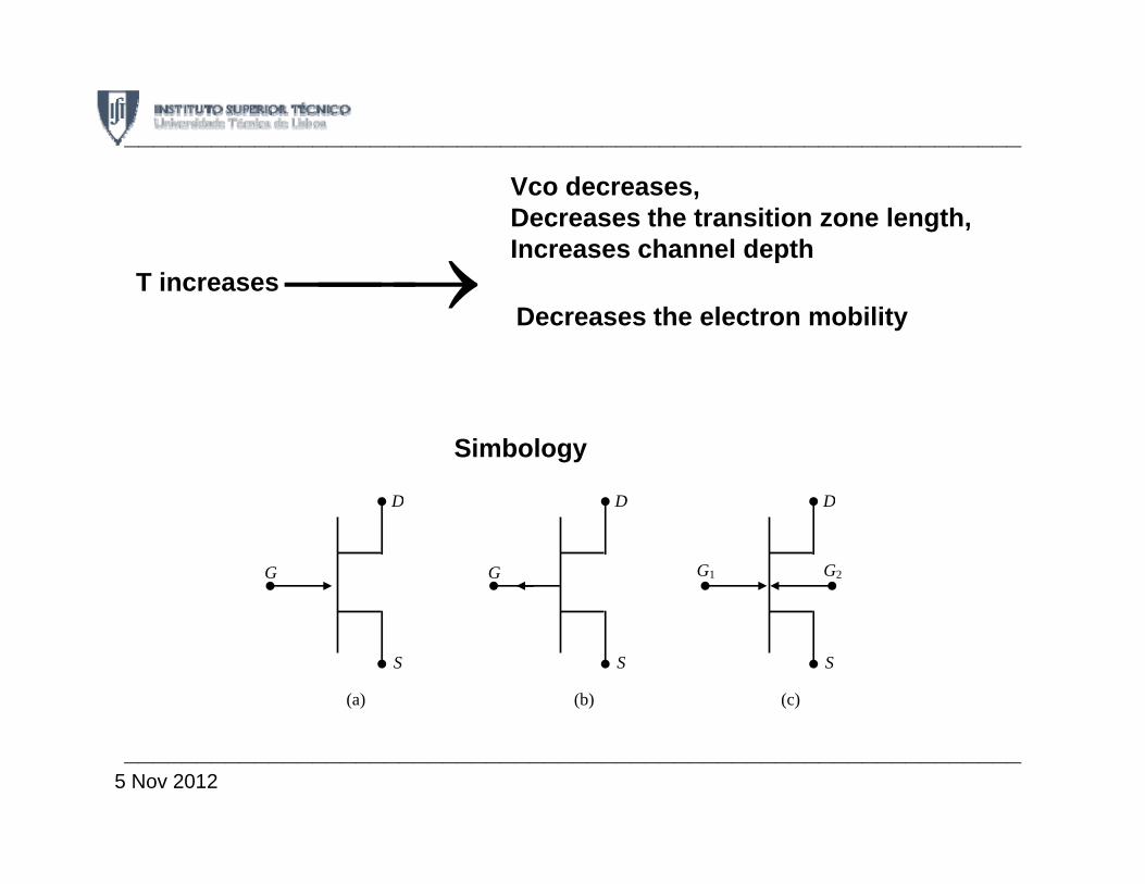
______________________________________________________________
T i →Vco decreases, Decreases the transition zone length,Increases channel depth
T increases ⎯→⎯Decreases the electron mobility
D D D
Simbology
G
D
G
D
G1
D
G2
S S S
(a) (b) (c)
______________________________________________________________5 Nov 2012

• Homogeneous semiconductor
R = d an p N N+ −− = −Electric neutralityRS
=σ
20 0 = ip n nThermal equilibrium
R G G G+
0 0 iq
Stationary situation with uniform illumination
tot ter efR rnp G G G= = = +
2 1 efi
ter
Gpn n
G⎛ ⎞
= +⎜ ⎟⎝ ⎠
07 Nov 2012 Ferreira Fernandes 1
ter⎝ ⎠
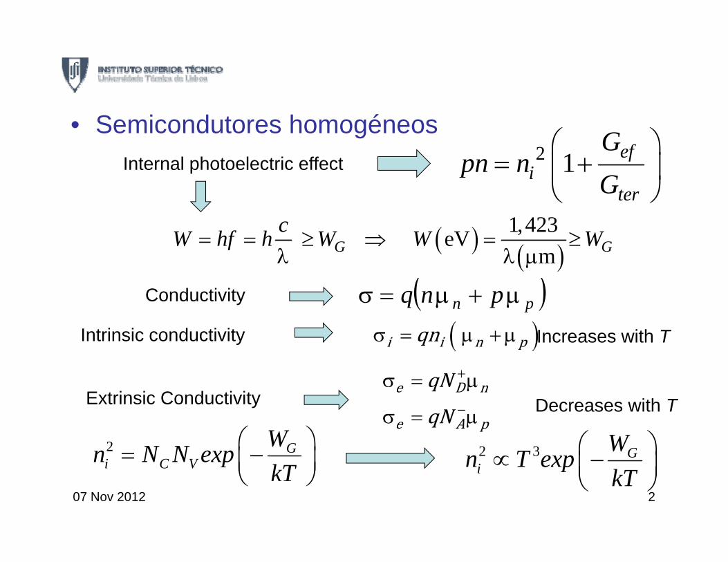
• Semicondutores homogéneos2 1 ef
iG
pn nG
⎛ ⎞= +⎜ ⎟Internal photoelectric effect i
terp
G⎜ ⎟⎝ ⎠
( ) ( )1,423eV= = ≥ ⇒ = ≥G G
cW hf h W W W
( )pn pnq μ+μ=σ
( ) ( )eV
m≥ ⇒ ≥
λ λ μG GW hf h W W W
Conductivity
Intrinsic conductivity ( )i i n pqnσ = μ + μ Increases with T
e D nqN +σ = μ
2 GWn N N exp ⎛ ⎞= −⎜ ⎟ 2 3 GWn T exp ⎛ ⎞∝ ⎜ ⎟
Decreases with TExtrinsic Conductivity e D n
e A p
qqN −
μ
σ = μ
07 Nov 2012 2
i C Vn N N expkT
= ⎜ ⎟⎝ ⎠ in T exp
kT∝ −⎜ ⎟
⎝ ⎠
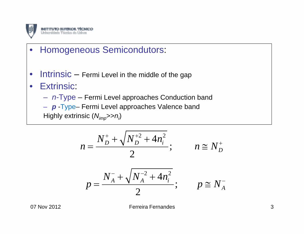
• Homogeneous Semicondutors:
• Intrinsic F i L l i th iddl f th• Intrinsic – Fermi Level in the middle of the gap
• Extrinsic:– n-Type – Fermi Level approaches Conduction band– p -Type– Fermi Level approaches Valence bandHighly extrinsic (Nimp>>ni)
2 24;
2D D i
D
N N nn n N
+ +++ +
= ≅
2 24;
2A A i
A
N N np p N
− −−+ +
= ≅2
07 Nov 2012 3Ferreira Fernandes
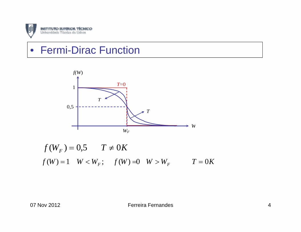
• Fermi-Dirac Function
f(W)f(W)
1
T
T=0
0,5
WW
T
WF
KTWf F 05,0)( ≠=KTWWWfWWWf 00)(1)( KTWWWfWWWf FF 00)(;1)( =>=<=
07 Nov 2012 4Ferreira Fernandes
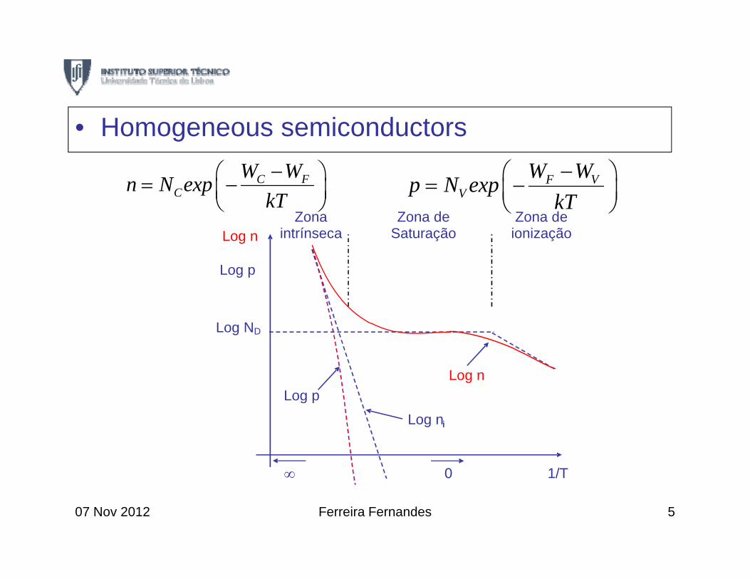
• Homogeneous semiconductors
C FW WN −⎛ ⎞⎜ ⎟
F VW WN −⎛ ⎞⎜ ⎟
C FCn N exp
kT⎛ ⎞= −⎜ ⎟⎝ ⎠
F VVp N exp
kT⎛ ⎞= −⎜ ⎟⎝ ⎠ Zona
intrínseca Zona de
Saturação Zona de
ionizaçãoLog n
Log N
Log p
Log ND
Log pLog n
Log p
Log n i
1/T0∞
i
1/T0 ∞
07 Nov 2012 5Ferreira Fernandes
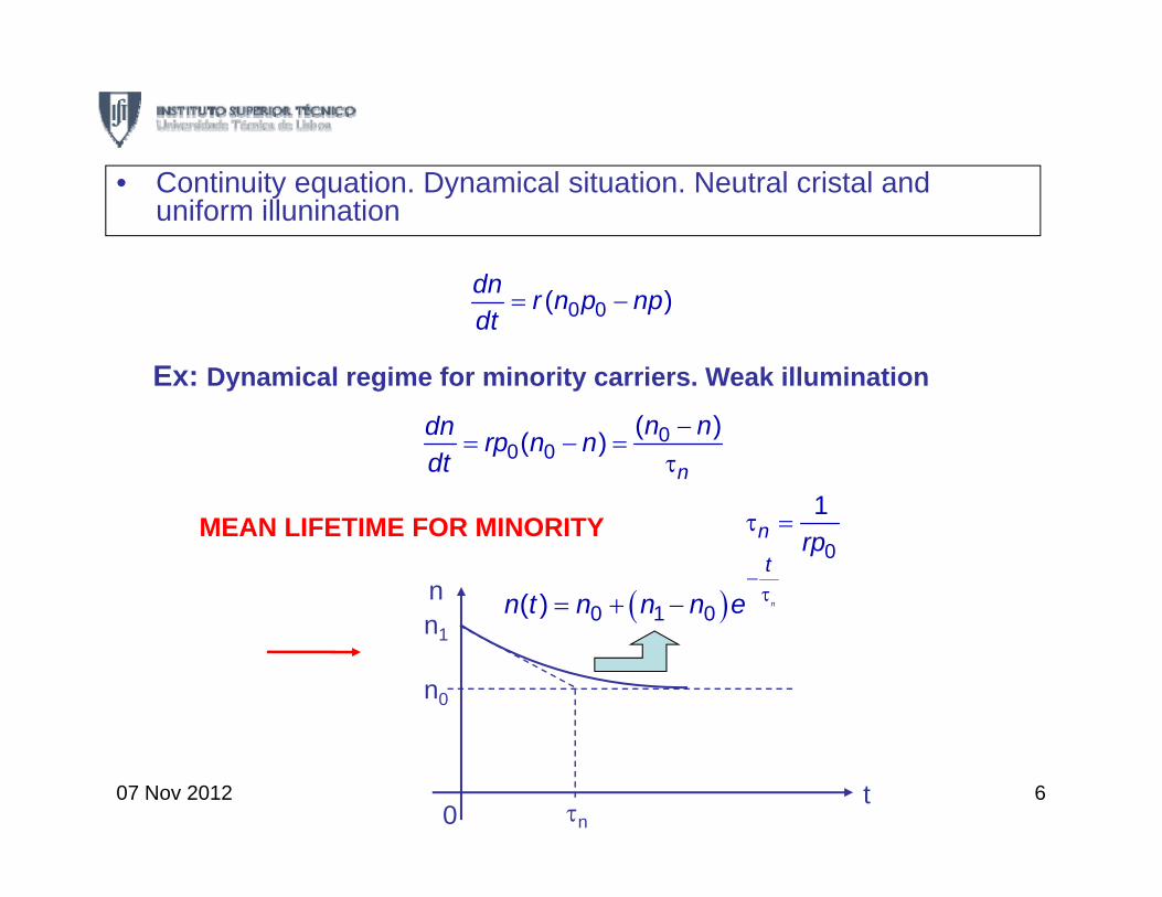
• Continuity equation. Dynamical situation. Neutral cristal and uniform illunination
dn0 0( )dn r n p np
dt= −
Ex: Dynamical regime for minority carriers. Weak illumination
00 0
( )( )n
n ndn rp n ndt
−= − =
τ
1MEAN LIFETIME FOR MINORITY
0
1n rpτ =
n ( )0 1 0( ) n
t
n t n n n e−τ= + −
n1
n0
( )0 1 0( )
τn0t07 Nov 2012 6
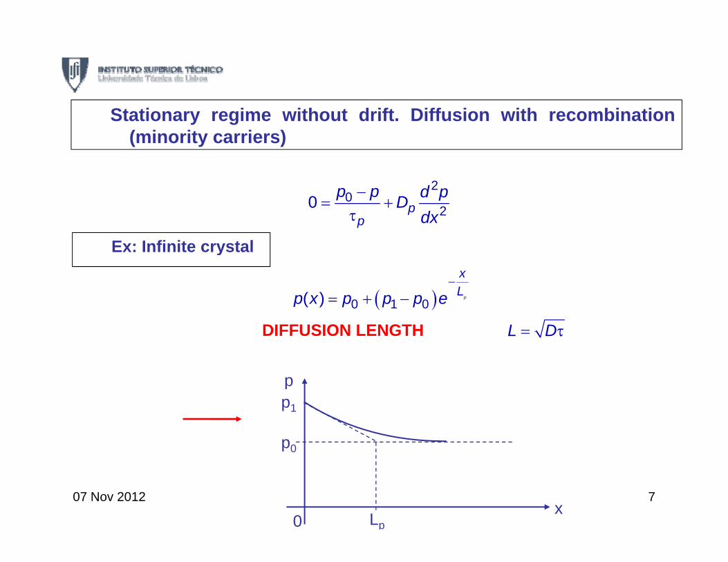
Stationary regime without drift. Diffusion with recombination(minority carriers)
20
20 pp
p p d pDdx
−= +
τ
Ex: Infinite crystalEx: Infinite crystal
( )0 1 0( ) p
xLp x p p p e
−= + −
DIFFUSION LENGTH L D= τ
pp1
p
p0
Lp0x
07 Nov 2012 7
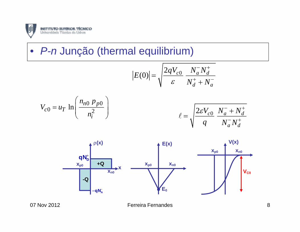
02( ) c a dqV N N− +
• P-n Junção (thermal equilibrium)
02(0) c a d
d a
qV N NEN N+ −=
+ε
0 0n p⎛ ⎞
02 c a d
a d
V N Nq N N
− +
− ++
=ε
0 00 2ln n p
c Ti
n pV u
n
⎛ ⎞= ⎜ ⎟⎜ ⎟
⎝ ⎠
E(x)
xp0 xn0
V(x) ρ(x)
DqN+
xp0 xn0
E0
VC0 x
xp0
xn0
Dq
N
+Q
-Q
E0AqN−−
07 Nov 2012 8Ferreira Fernandes
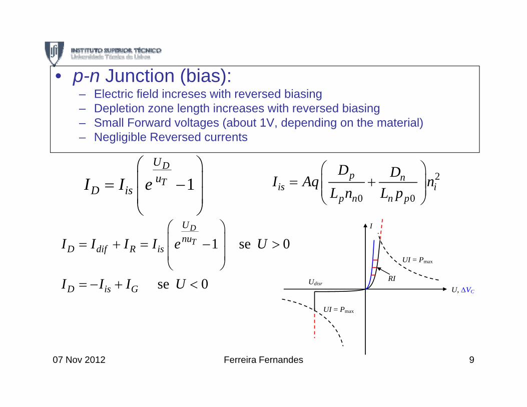
• p n Junction (bias):• p-n Junction (bias):– Electric field increses with reversed biasing– Depletion zone length increases with reversed biasing– Small Forward voltages (about 1V, depending on the material)
DUu
⎛ ⎞⎜ ⎟ 2p nD DI A
⎛ ⎞⎜ ⎟
Small Forward voltages (about 1V, depending on the material)– Negligible Reversed currents
1TuD isI I e⎜ ⎟= −
⎜ ⎟⎝ ⎠
2
0 0
p nis i
p n n pI Aq n
L n L p= +⎜ ⎟⎜ ⎟
⎝ ⎠
DU⎛ ⎞ I
1 se 0
0
DTnu
D dif R isI I I I e U
I I I U
⎛ ⎞⎜ ⎟= + = − >⎜ ⎟⎝ ⎠ UI = Pmax
U RIse 0D is GI I I U= − + <
UI = Pmax
U, ΔVC Udisr RI
07 Nov 2012 9Ferreira Fernandes

p n J nction ( ariable regime)
DU
• p-n Junction (variable regime)
TnuT is
dT
I eCnu
=τ
0D isD I IIg
U nU⎛ ⎞ +∂
= =⎜ ⎟∂⎝ ⎠
PFR( , )D DI U
D TPFRU nU∂⎝ ⎠
1
( ) ( )1202
A DT C D
A D
qN NC A V UN N
−ε= −
+
07 Nov 2012 10Ferreira Fernandes
J ti ( l t t ti i )• p-n Junction (almost-stationary regime)
ID R
ID
MVR
UDsinωMV t
UD−VM UD
VM
− MVR
07 Nov 2012 11Ferreira Fernandes
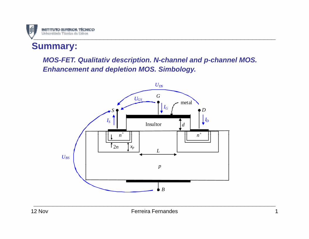
S mmar______________________________________________________________Summary:
MOS-FET. Qualitativ description. N-channel and p-channel MOS. Enhancement and depletion MOS. Simbology.
G metal
UDS
UGS
n+ n+
IG D
ID
S
IS d Insultor
n n
2n xp L
UBS
p
B
______________________________________________________________12 Nov 1Ferreira Fernandes
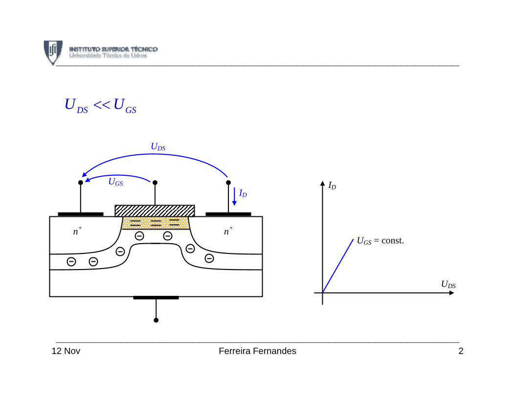
______________________________________________________________
DS GSU U<<
UDS
UGS ID
ID
n+ n+ UGS = const.
UDS
______________________________________________________________12 Nov 2Ferreira Fernandes
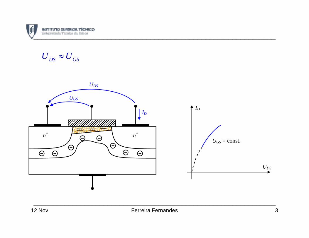
______________________________________________________________
≈DS GSU U
UGS
UDS
ID
+ +
ID
n+ n+
UGS = const.
UDS
______________________________________________________________12 Nov 3Ferreira Fernandes
______________________________________________________________
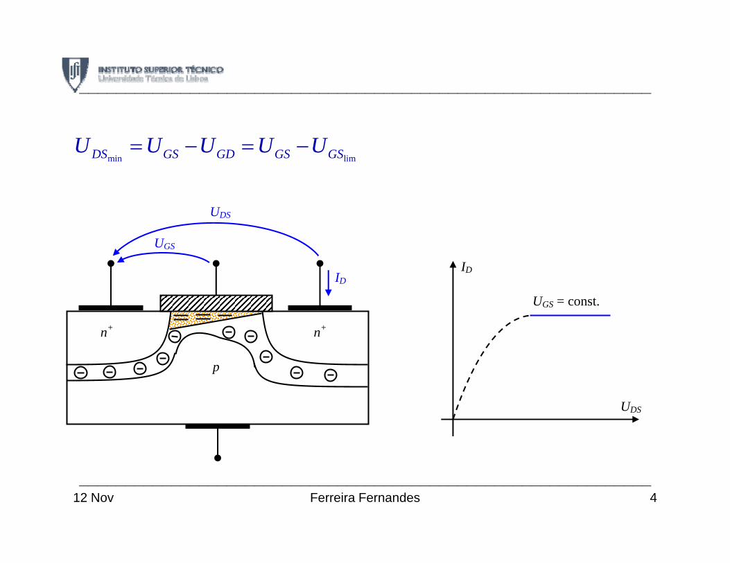
min lim= − = −DS GS GD GS GSU U U U U
UGS
UDS
UGS
ID ID
UGS = const.
n+ n+
p
UDS
______________________________________________________________12 Nov 4Ferreira Fernandes
______________________________________________________________
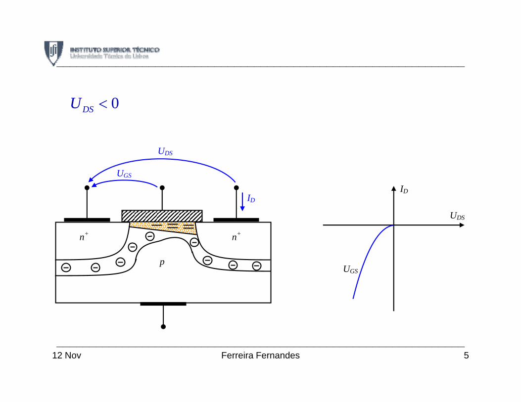
0<DSU
UGS
UDS
UGS
ID ID
UDS
n+ n+
UGS p
______________________________________________________________12 Nov 5Ferreira Fernandes
______________________________________________________________
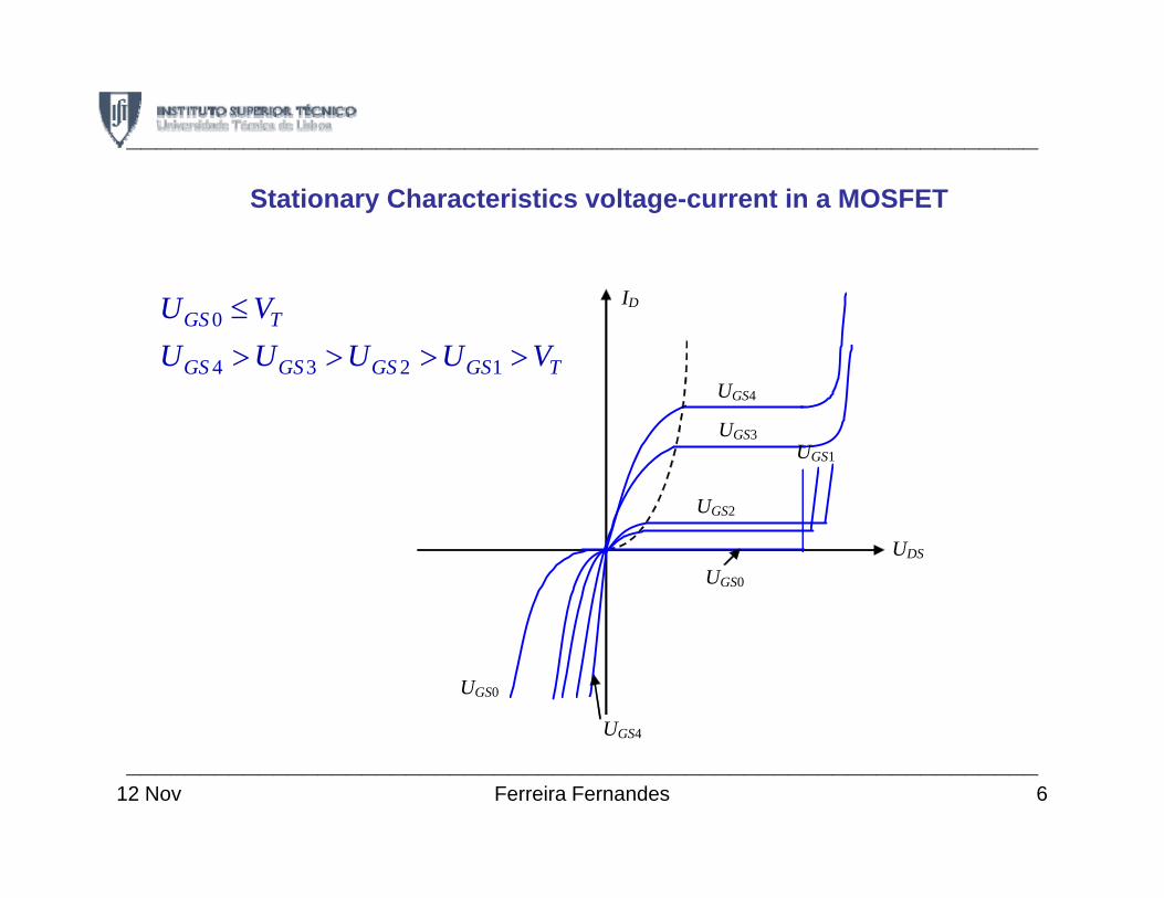
Stationary Characteristics voltage-current in a MOSFET
UGS4
ID 0
4 3 2 1
≤
> > > >GS T
GS GS GS GS T
U VU U U U V
UGS4
UGS3
U
UGS1
UGS2
UGS0 UDS
UGS0
UGS4UGS4
______________________________________________________________12 Nov 6Ferreira Fernandes
______________________________________________________________
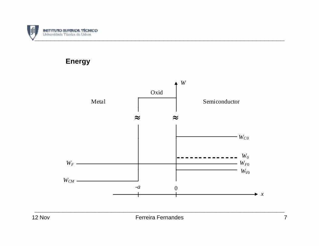
Energy
MetalOxid
Semiconductor
W
≈ ≈
WC0
WF
WC0
W0 WF0
W
x -a 0
WCM WV0
______________________________________________________________12 Nov 7Ferreira Fernandes
______________________________________________________________
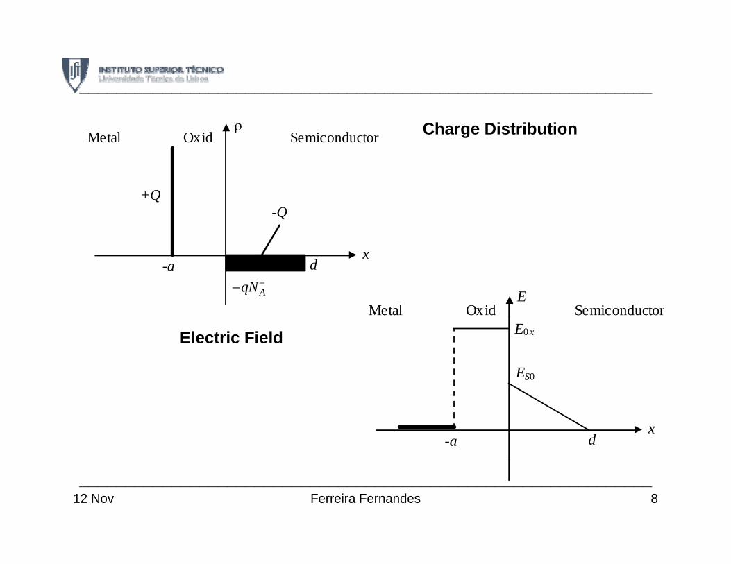
ρ Metal Semiconductor Oxid Charge Distribution
+Q -Q
x-a d
−− AqN E Metal SemiconductorOxid
ES0
E0 xElectric Field
x -a d
______________________________________________________________12 Nov 8Ferreira Fernandes
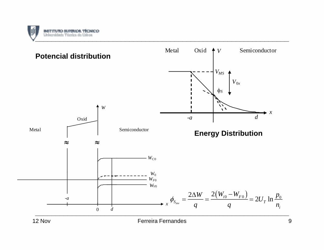
______________________________________________________________ V Metal Semiconductor Oxid
VMS
Potencial distribution
φS
V0x
Wx
-a d
Energy DistributionMetal
Oxid
Semiconductor
≈ ≈
WC0
W
( )0 0 022 2 lninv
i FS T
W W pW Uq q n
φ−Δ
= = =x
-a
W0WF0
WV0
inviq q nx
0 d ______________________________________________________________12 Nov 9Ferreira Fernandes
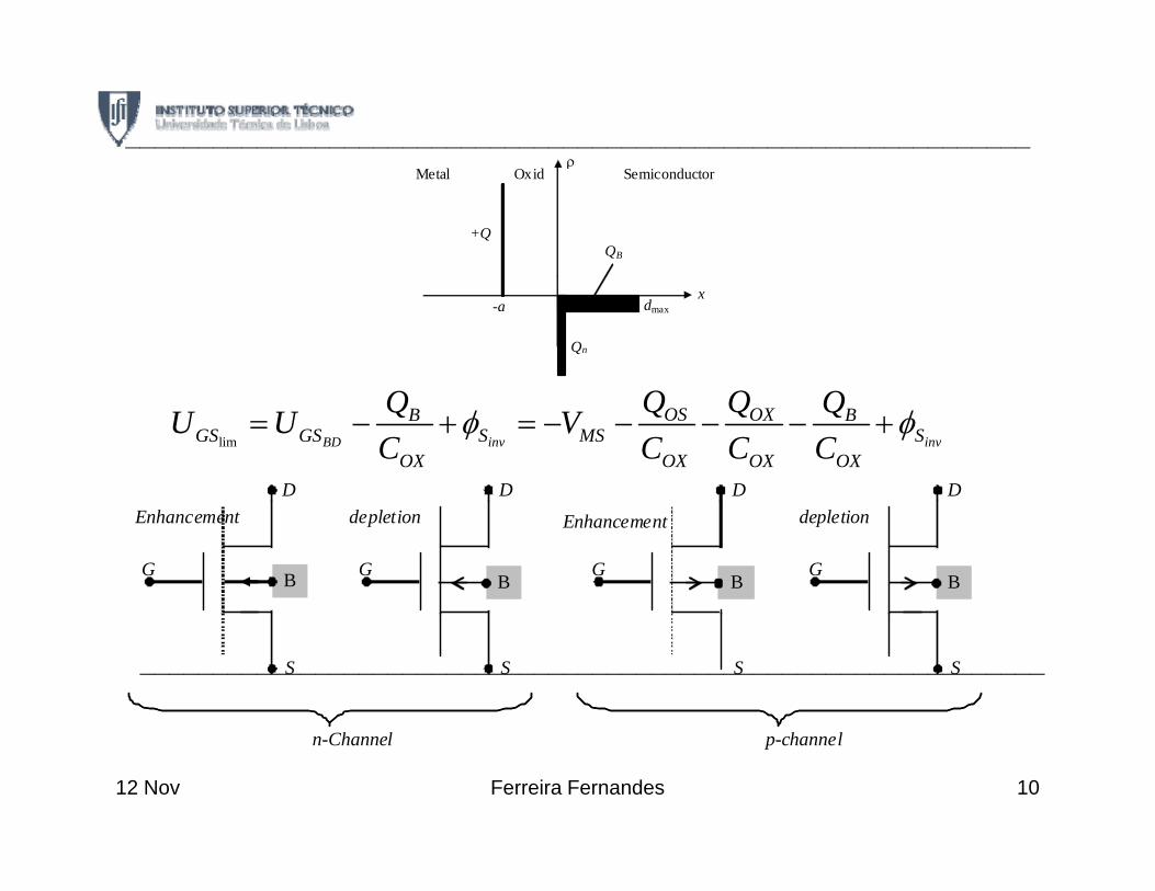
ρ ______________________________________________________________
ρ Metal Semiconductor Oxid
+Q QB
x -a dmax
Qn
lim BD inv inv
OS OXB BGS GS S MS S
OX OX OX OX
Q QQ QU U VC C C C
φ φ= − + = − − − − +
D D D D
G
Enhancement
G
depletion
G
Enhancement
G
depletion
B B B B
S S S S ______________________________________________________________
n-Channel p-channel
12 Nov 10Ferreira Fernandes
S______________________________________________________________
Summary:Zones in MOSFET. Incremental components for MOSFET. Differential capacities. Body p p yeffect.
( ) ( )CS y x y b=
( ) ( ) ( , )
0( )
ˆ, ( , ) ( , )Cx y dV x yD y n dy
S y
I J u dS qbn x y x y dx= − =∫ ∫ μ( )y
( )( ) ( )*
0( , ) ( , ) ( )Cx ydV y dV y
D n n ndy dyI b qn x y x y dx b Q y= = −∫ μ μ
*
0( ) ( )DSU
nD nI b Q y dV y
L= − ∫
μ ( ) ( ) ( )n S BQ y Q y Q y= −
( ) 2B S A SQ y q N −= − ε φ
Ferreira Fernandes 1
( )invB S A SQ y q φ
______________________________________________________________19 Nov
______________________________________________________________
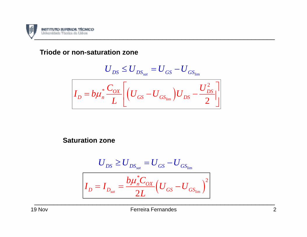
limsatDS DS GS GSU U U U≤ = −
Triode or non-saturation zone
( )lim
2*
2OX DS
D n GS GS DSC UI b U U U
L⎡ ⎤
= − −⎢ ⎥⎣ ⎦
μ
limsatDS DS GS GS
2L ⎣ ⎦
U U U U≥ = −
Saturation zone
( )lim
* 2
2sat
n OXD D GS GS
b CI I U UL
= = −μ
limsatDS DS GS GSU U U U≥ =
( )2L______________________________________________________________
2Ferreira Fernandes19 Nov
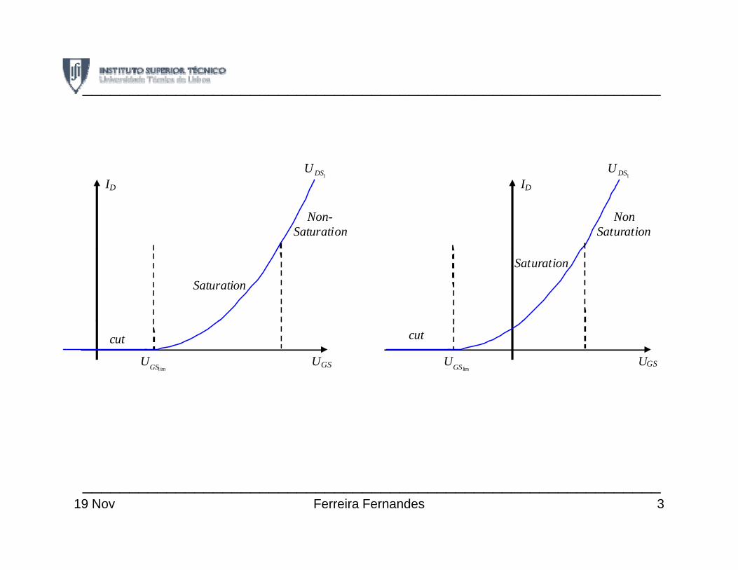
______________________________________________________________
1DSU
1DSUID
1
Non- Saturation
ID1
Non Saturation
Saturation
Saturation
UGS
cut
l imGSU UGSlimGSU
cut
3Ferreira Fernandes______________________________________________________________
19 Nov
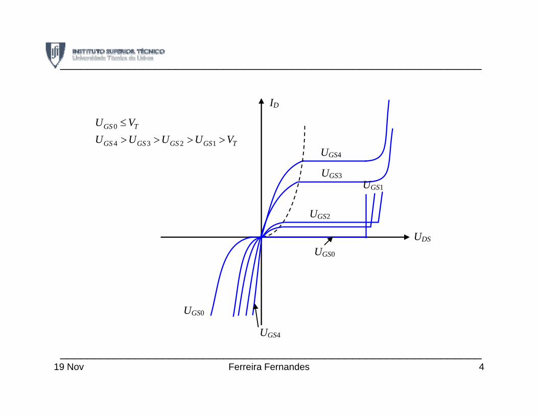
______________________________________________________________
ID
0 ≤GS TU V
UGS4
UGS3 U
4 3 2 1> > > >GS GS GS GS TU U U U V
UGS2
UGS1
UUGS0
UDS
UGS0
UGS4
4Ferreira Fernandes______________________________________________________________
19 Nov
______________________________________________________________
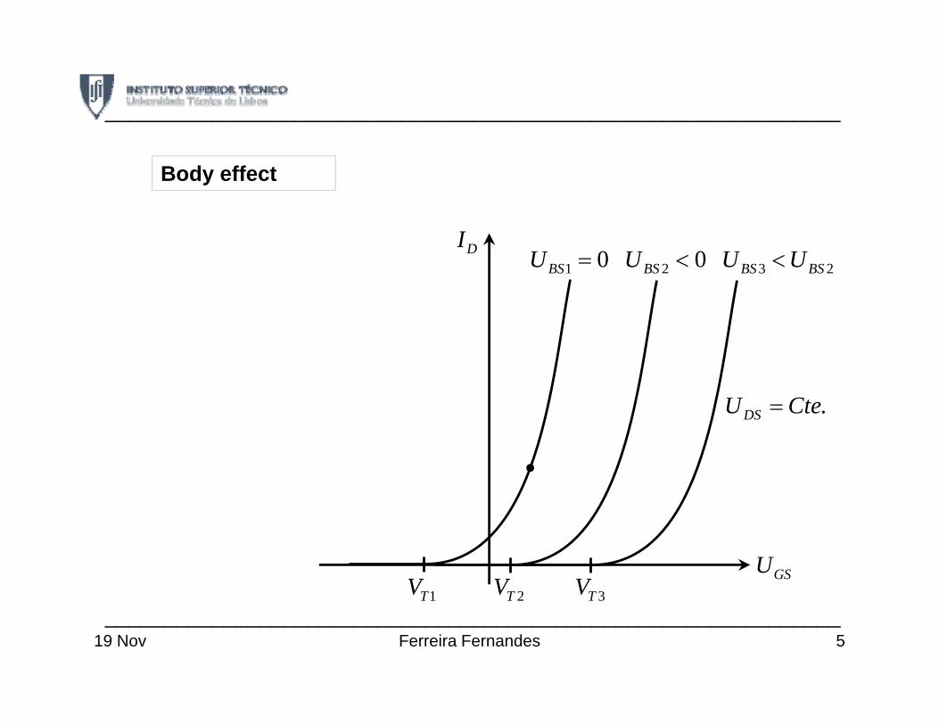
Body effect
DI1 0BSU = 2 0BSU < 3 2BS BSU U<
U Cte= .DSU Cte=
GSU1TV 2TV 3TV1TV 2TV 3TV
5Ferreira Fernandes______________________________________________________________
19 Nov
______________________________________________________________
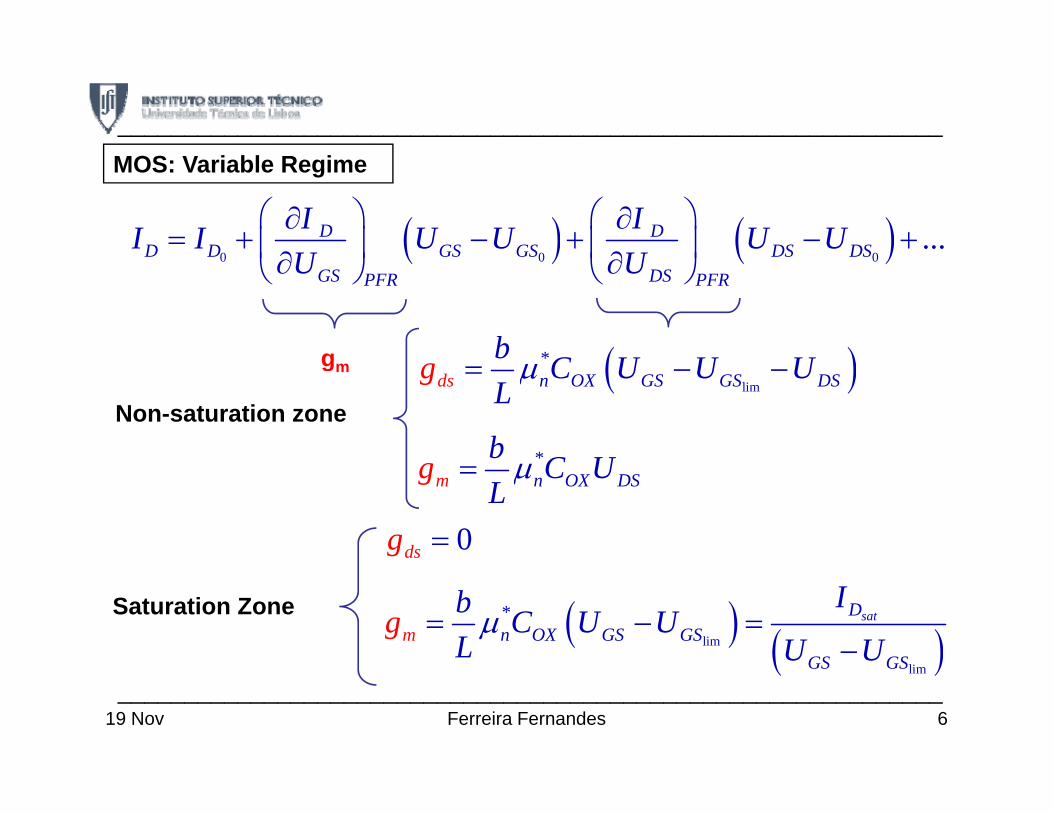
MOS: Variable Regime
( ) ( )0 0 0...D D
D D GS GS DS DSI II I U U U U
U U⎛ ⎞ ⎛ ⎞∂ ∂
= + − + − +⎜ ⎟ ⎜ ⎟∂ ∂⎝ ⎠ ⎝ ⎠( ) ( )0 0 0D D GS GS DS DS
GS DSPFR PFRU U⎜ ⎟ ⎜ ⎟∂ ∂⎝ ⎠ ⎝ ⎠
g ( )*bgm
*b C U
( )lim
*n OX GS GS Dd Ss
b C U U UL
g = − −μNon-saturation zone
*m n OX DSg b C U
L= μ
0dsg =
Saturation Zone ( ) ( )lim
* satm
Dn OX GS GS
GS GS
Ib C U UL U U
g = − =−
μ( )limGS GS
6Ferreira Fernandes______________________________________________________________
19 Nov
______________________________________________________________
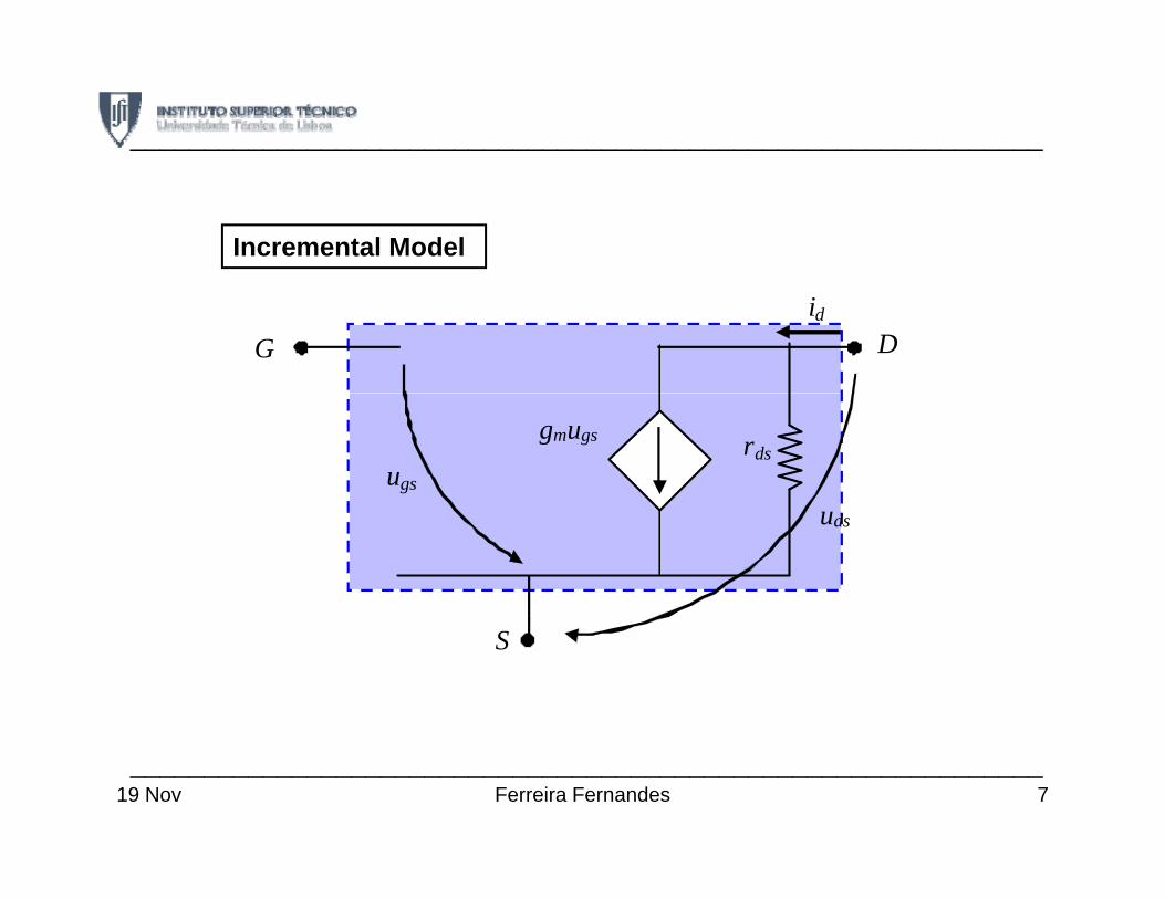
Incremental Model
id D G
ugs
gmugs rds
uds
S
7Ferreira Fernandes______________________________________________________________
19 Nov
______________________________________________________________
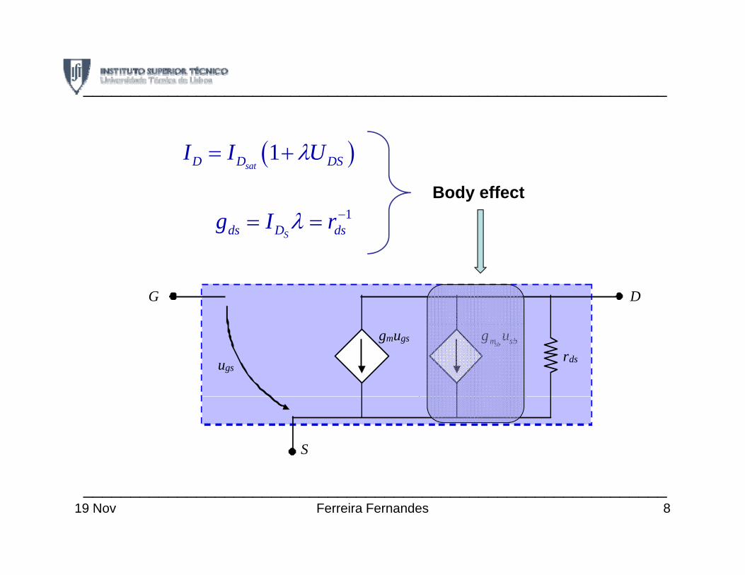
( )1satD D DSI I U= +λ
1Sds D dsg I r−= =λ
Body effect
D G
rds ugs
gmugs sbm sbg u
S
Ferreira Fernandes 8______________________________________________________________
19 Nov
______________________________________________________________
( )⎡ ⎤
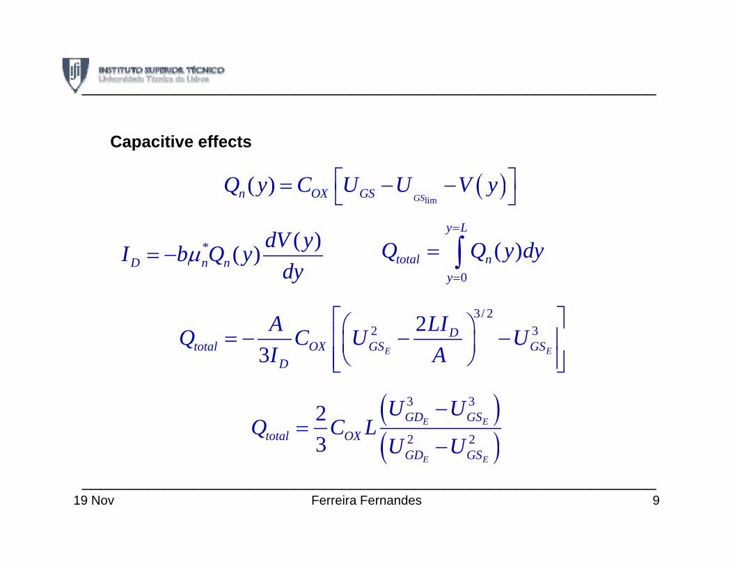
Capacitive effects
( )lim
( )GSn OX GSQ y C U U V y⎡ ⎤= − −⎣ ⎦
* ( )( ) dV yI b Q ( )y L
Q Q d=
∫( )( )D n nyI b Q y
dy= − μ
0
( )total ny
Q Q y dy=
= ∫
3/ 22A LI⎡ ⎤⎛ ⎞2 323 E E
Dtotal OX GS GS
D
A LIQ C U UI A
⎡ ⎤⎛ ⎞= − − −⎢ ⎥⎜ ⎟⎝ ⎠⎢ ⎥⎣ ⎦
( )( )
3 3
2 2
23
E E
E E
GD GStotal OX
GD GS
U UQ C L
U U
−=
−
9Ferreira Fernandes______________________________________________________________
( )E E
19 Nov
______________________________________________________________
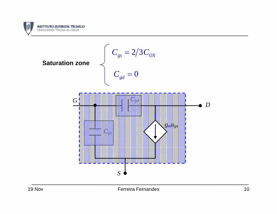
2 3gs OXC C=Saturation zone
0gdC =
D
G Cgd
Cgs gmugs
S
10Ferreira Fernandes______________________________________________________________
S
19 Nov
______________________________________________________________
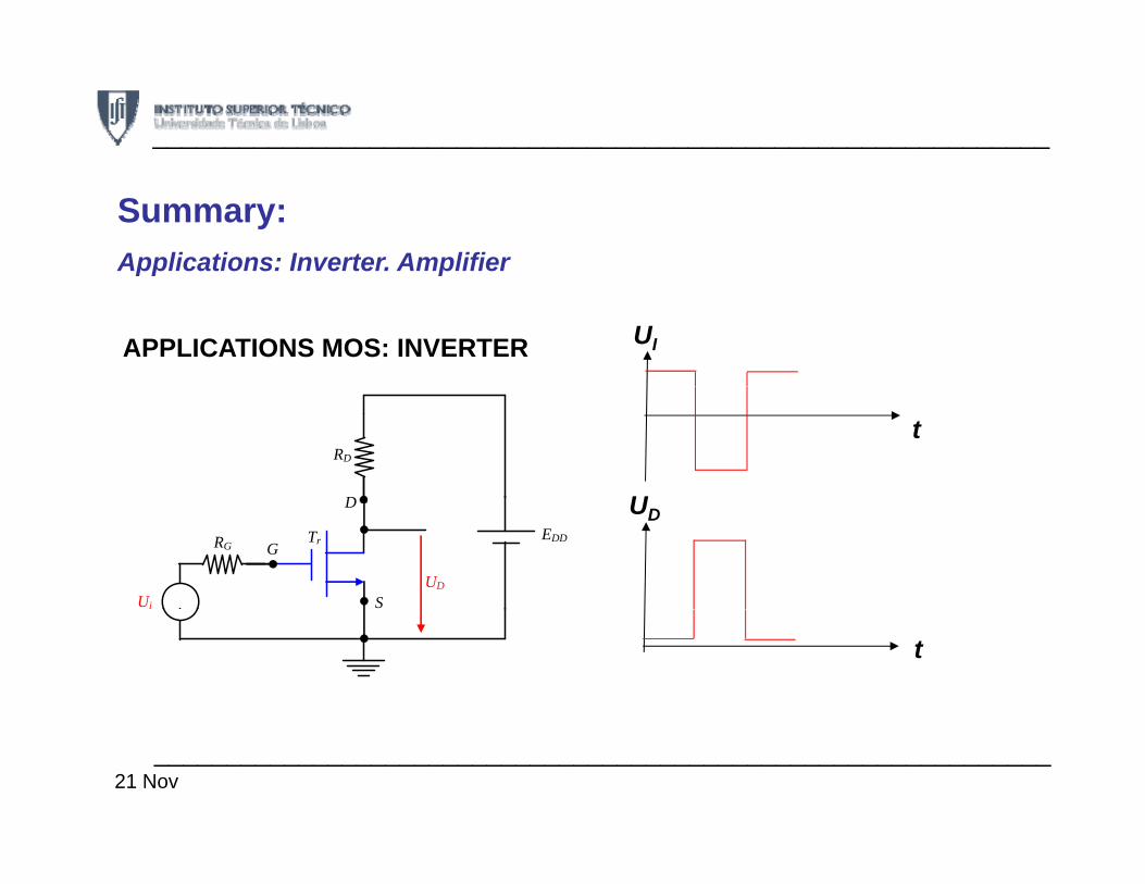
Summary:Applications: Inverter. Amplifier
APPLICATIONS MOS: INVERTER
pp p
UI
RD
D U
t
EDD
UDUi
D
Tr
S
G RG
UD
t
______________________________________________________________21 Nov
______________________________________________________________
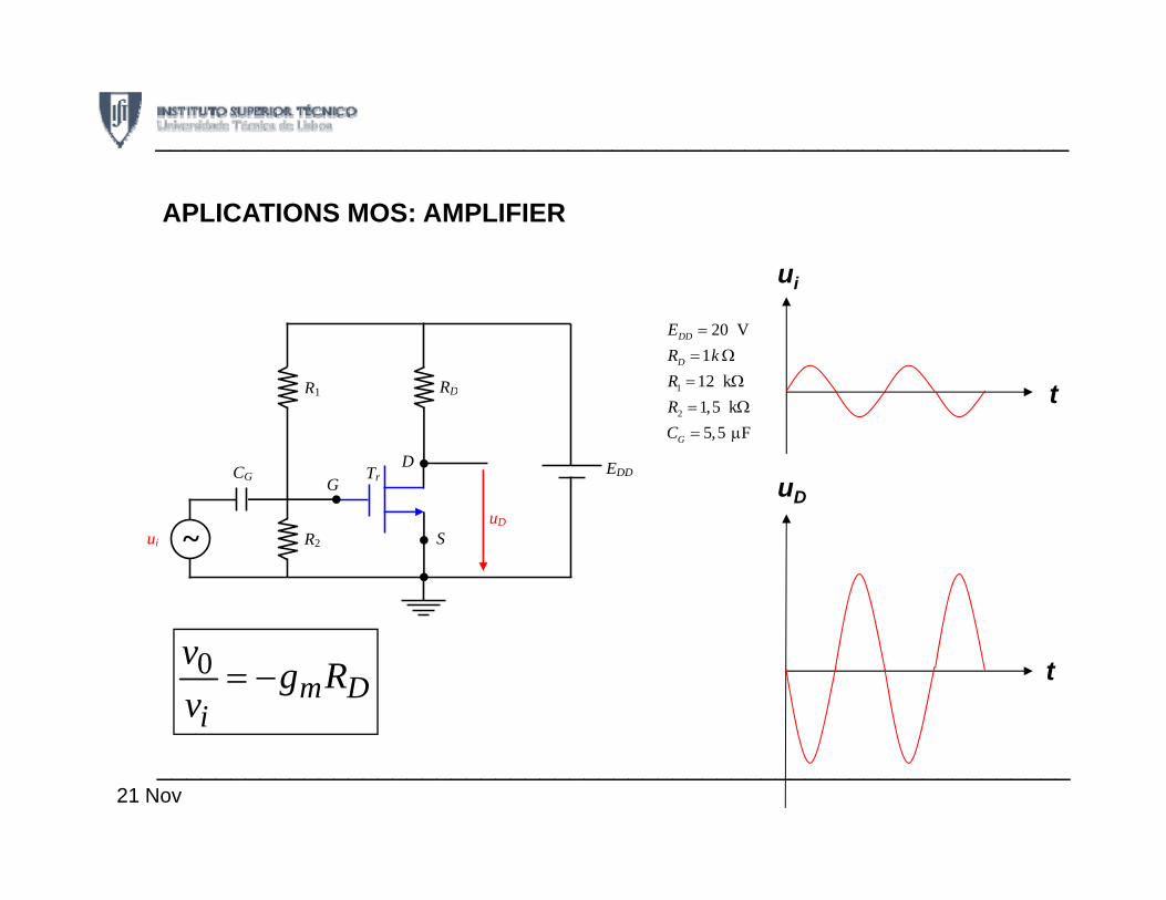
APLICATIONS MOS: AMPLIFIER
ui
RD 1
20 V1
12 k
DD
D
ER kR
== Ω= ΩR1
ui
tD
EDDD
Tr
2 1,5 k5,5 FG
RC
= Ω= μ
1
CG G
t
uDuD
ui S R2 ~
t0m D
i
v g Rv
= −
______________________________________________________________21 Nov
R
______________________________________________________________ RD
ID (mA)
EDRG = 10 kΩ
G
D ID
I1
UDS
P
0
1
1
ED
EG=10 V
G
S
IG
UGS
RSUGS(V)0-1 S
(a) (b) ID
Q
O
( )*D D SE R R+
( )D D SE R R+
2 VGSU =
U
O
UDS*DE DE ODSU
QDSU______________________________________________________________21 Nov
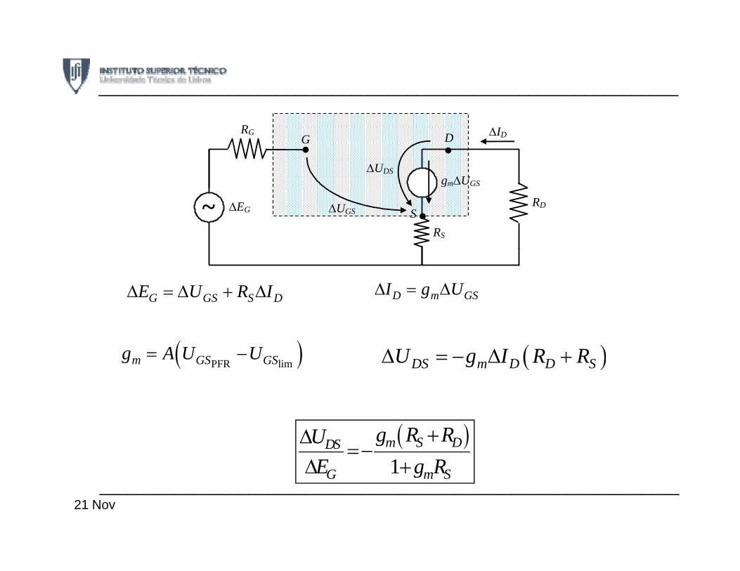
______________________________________________________________
RG
G
ΔUDS
D ΔID
ΔU
ΔEG ~ ΔUGS
RS
RD S
gmΔUGS
G GS S DE U R IΔ = Δ + Δ Δ = ΔD m GSI g U
( )DS m D D SU g I R RΔ = − Δ +( )PFR lim= −m GS GSg A U U
( )1
+Δ=−
Δ +m S DDS g R RU
E g R1Δ +G m SE g R______________________________________________________________
21 Nov

______________________________________________________________
Summary:Thyristor. Stationary characteristic I(U). SCR.TRIAC. DIAC. GTO.
I E
II
I
B IL
IH
UUB0
H
Current-voltage characterístic of a thyristor in the 1st quadrant
Ferreira Fernandes 1
Current voltage characterístic of a thyristor in the 1st quadrant______________________________________________________________
14 Nov
______________________________________________________________
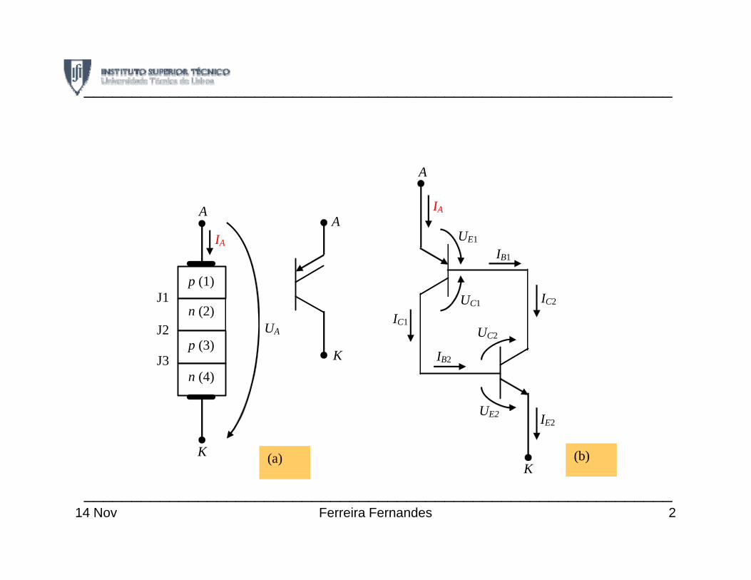
A
A
IA
IA
IUE1
A
U
J1
J2
p (1)
n (2)
IB1
IC1
IC2UC1
UAJ2
J3 p (3)
n (4) IB2
UC2
K
K
IE2
K
UE2
(a) (b) K
2Ferreira Fernandes______________________________________________________________
14 Nov
______________________________________________________________
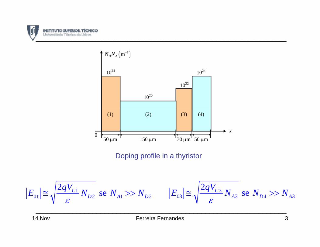
1024 1024
( )3mD AN N −
1022
1020
(1) (2) (3) (4)
0 x
50 μm 150 μm 50 μm30 μm50 μm 150 μm 50 μm30 μm
Doping profile in a thyristor
101 2 1 2
2 seCD A D
qVE N N N≅ >>ε
303 3 4 3
2 seCA D A
qVE N N N≅ >>εε ε
3Ferreira Fernandes______________________________________________________________
14 Nov
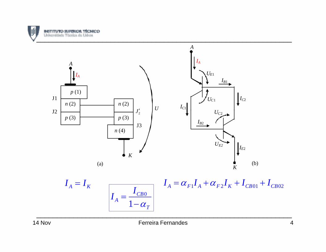
A______________________________________________________________
A
IA
A
IA
IUE1
J1
J2
p (1)
n (2)
IB1
IC1
IC2UC1
Un (2)
J ′ UJ2
J3 p (3)
IB2
UC2
U
p (3)
n (4)
2J ′ U
KIE2
K
UE2
(a) (b)
A KI I= 1 2 01 02A F A F K CB CBI I I I I= + + +α α0
1CB
AT
II =−α1 Tα
4Ferreira Fernandes______________________________________________________________
14 Nov
______________________________________________________________
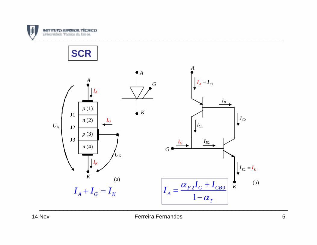
A A
SCR
A
IA
(1)
1EAI I=
IB1
G
UA
J1
J2
J3
p (1)
p (3)
n (2) IC1
IC2IG
K
J3 n (4)
IB2
2 KEI I=IK
UGG
IG
K 2 KEI I
K (a) (b)
2 0
1F G CB
AT
I II +=
−α
αA G KI I I+ =1 Tα
5Ferreira Fernandes______________________________________________________________
14 Nov
______________________________________________________________
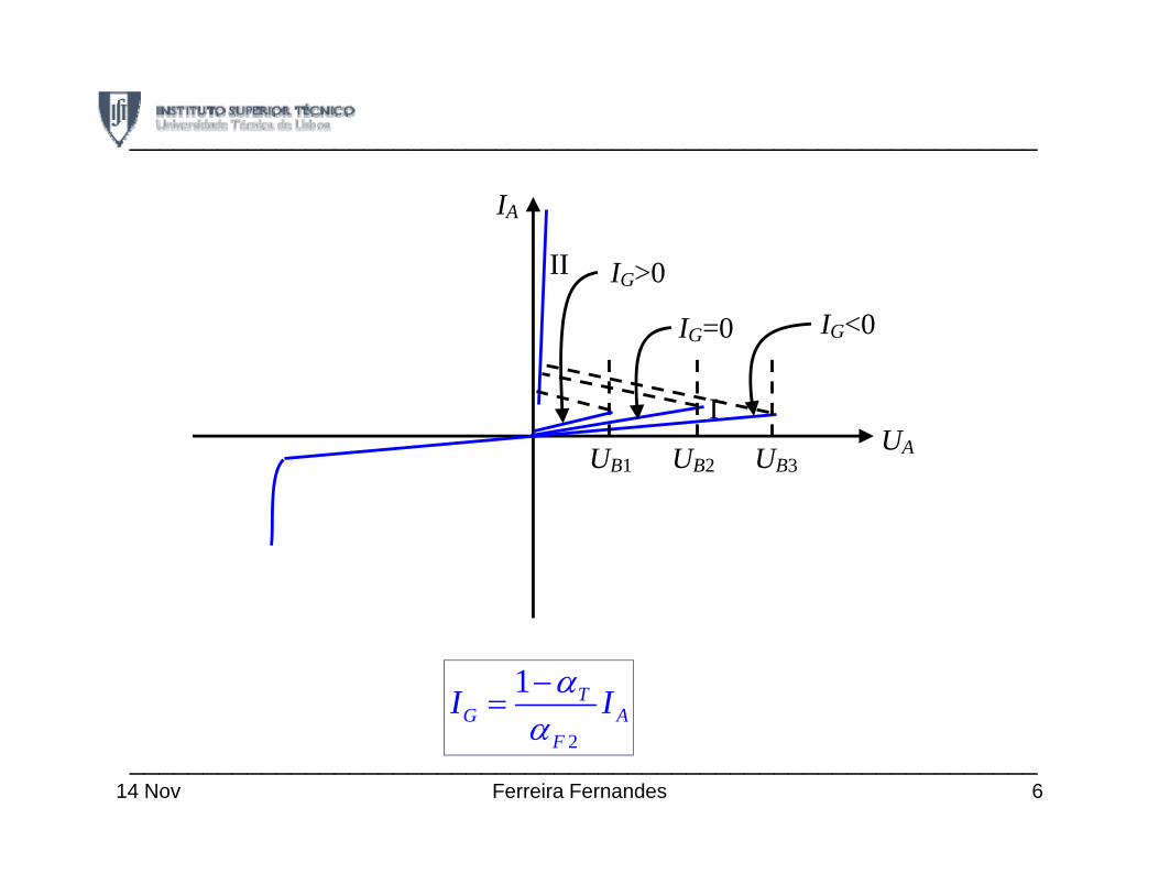
II
IA
IG>0IG>0
IG=0 IG<0
I UAUB3 UB2 UB1
1 TG AI I−=
αα 2Fα
6Ferreira Fernandes______________________________________________________________
14 Nov
______________________________________________________________
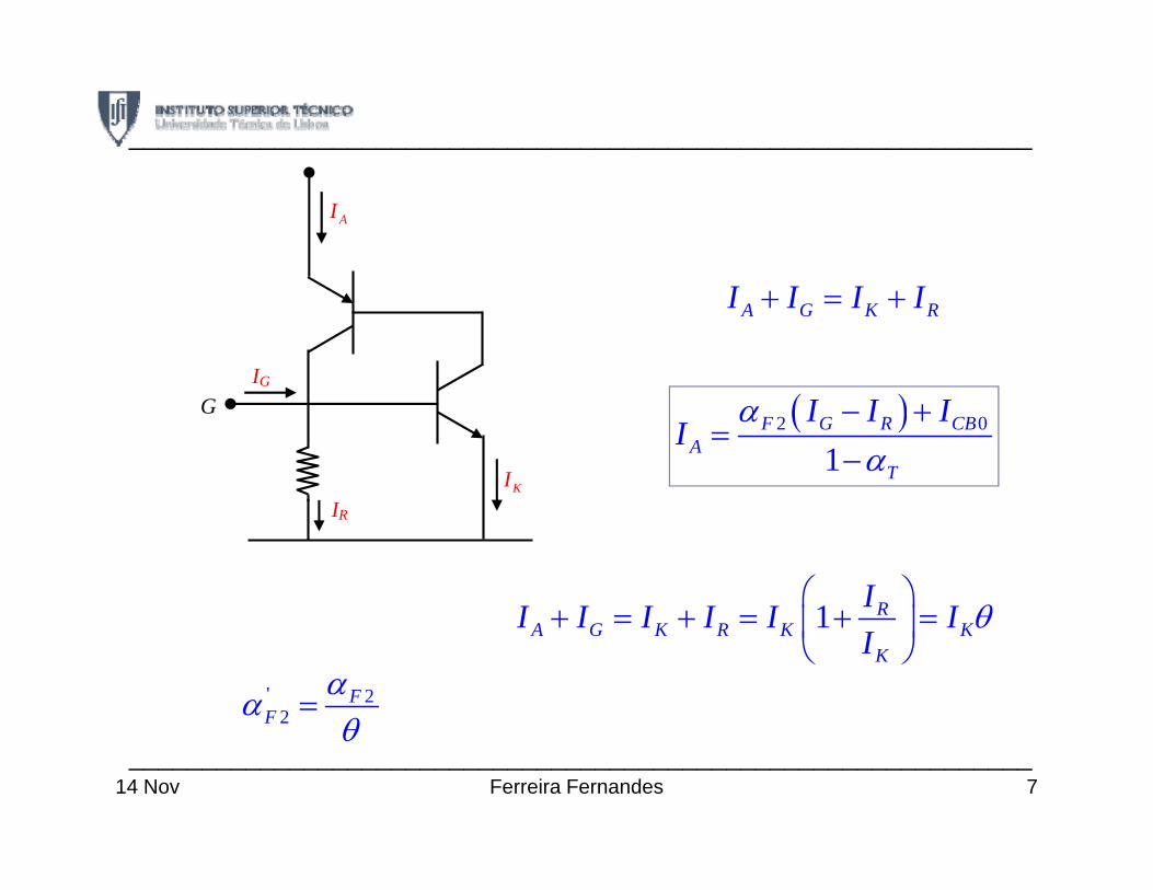
AI
IG
A G K RI I I I+ = +
KI
G ( )2 0
1F G R CB
AT
I I II
− +=
−α
αIR
1 RII I I I I I⎛ ⎞
+ + +⎜ ⎟ θ1 RA G K R K K
K
I I I I I II
+ = + = + =⎜ ⎟⎝ ⎠
θ
' 22
FF =
ααθθ
7Ferreira Fernandes______________________________________________________________
14 Nov

IA
p
n ( )11 AI−αElectrons
1 AIα
ICB01 Holes
IG
p
2 KIα
ICB02
( )21 KI−α
n
IK 814 Nov
______________________________________________________________
n
A
IA
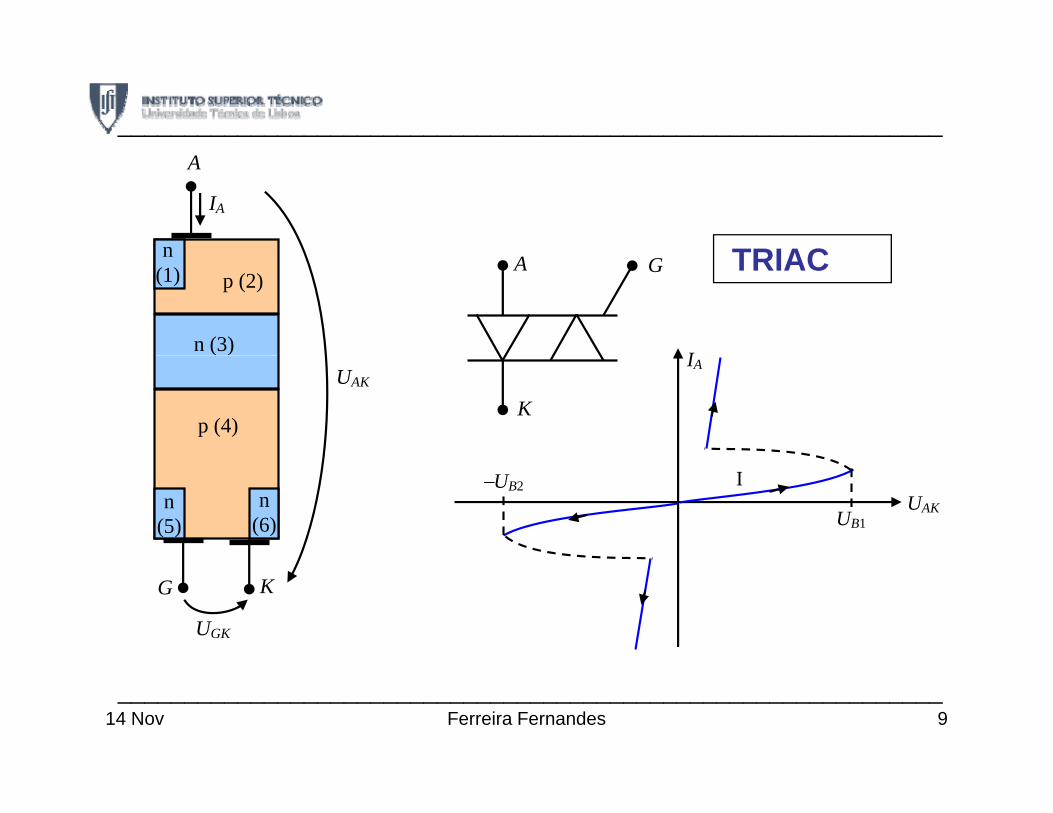
TRIACn (1) p (2)
n (3)
A G TRIAC
I
p (4)
UAK K
IA
n (5)
n (6)
I
UB1
−UB2 UAK
G K
UGK
9Ferreira Fernandes______________________________________________________________
14 Nov
28 Nov 1Ferreira Fernandes
______________________________________________________________
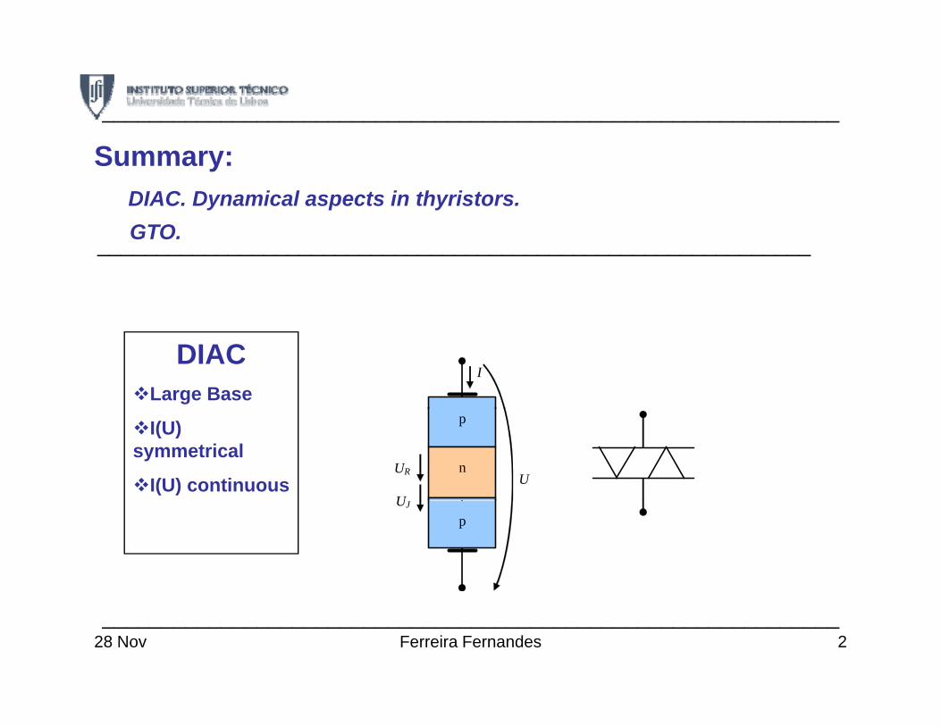
Summary:DIAC. Dynamical aspects in thyristors. GTOGTO.____________________________________________________________
DIACLarge Base
I
I(U) symmetrical
I(U) continuous
p
n U
U
UR
p UJ
______________________________________________________________2Ferreira Fernandes28 Nov
______________________________________________________________
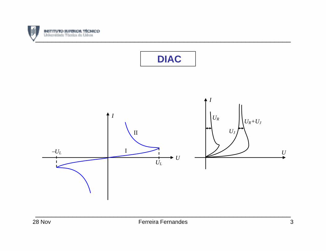
DIAC
I
I
II
UR
UJ UR+UJ
I
UL
−UL U
U
______________________________________________________________3Ferreira Fernandes28 Nov
______________________________________________________________
IA
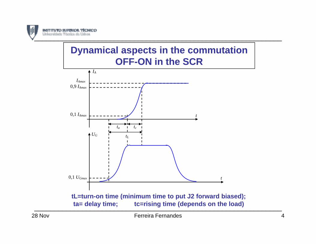
Dynamical aspects in the commutation OFF-ON in the SCR
IAmax 0,9 IAmax
t 0,1 IAmax
UG ta tc
tLtL
t 0,1 UGmax
tL=turn-on time (minimum time to put J2 forward biased); ( p );ta= delay time; tc=rising time (depends on the load)______________________________________________________________
4Ferreira Fernandes28 Nov
______________________________________________________________
Uext
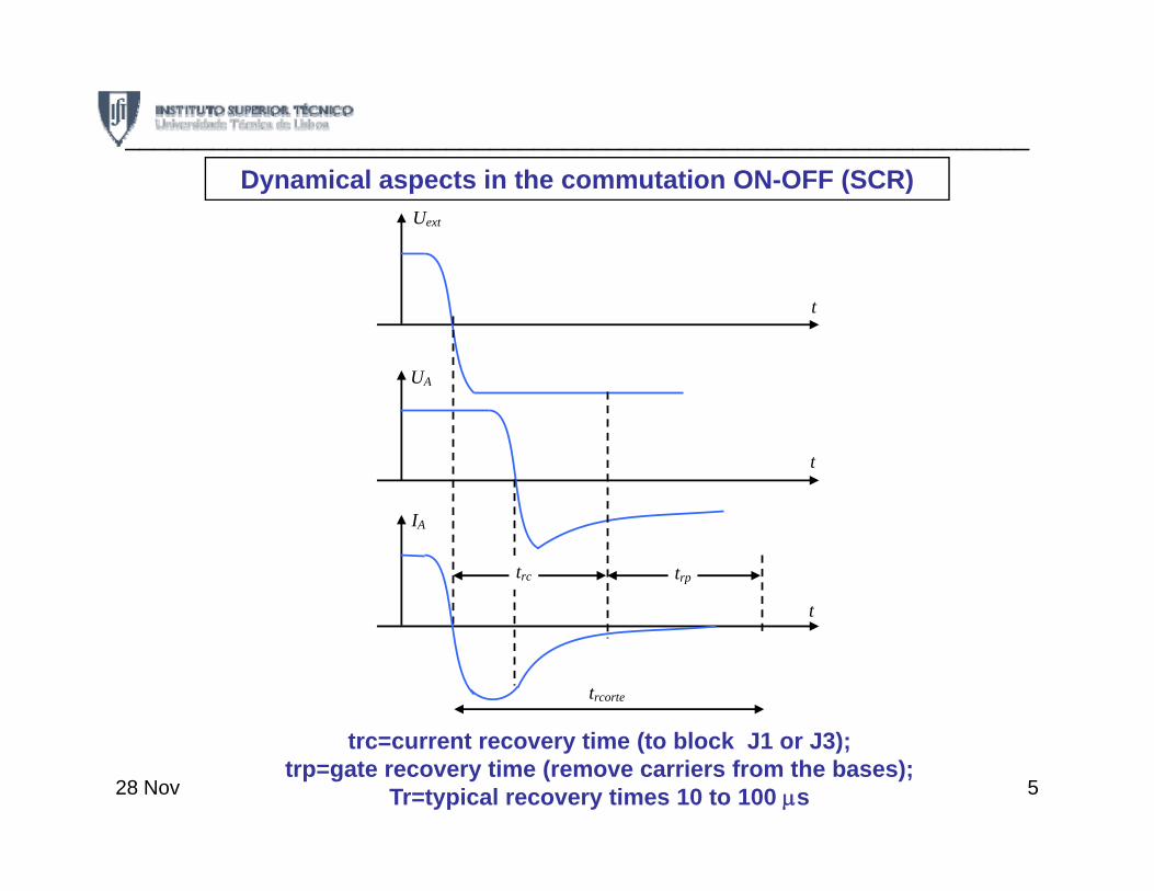
Dynamical aspects in the commutation ON-OFF (SCR)
UA
t
t
IA
t
trc trp
t
trcorte
trc=current recovery time (to block J1 or J3); trp=gate recovery time (remove carriers from the bases);
Tr=typical recovery times 10 to 100 μs28 Nov 5

______________________________________________________________
GTOGate controls commutation in both directions
Natural commutation in ACNatural commutation in AC
Forced commutation in CC (Increase of load or short circuit)
GTO- commutation also with gate negative pulses
GTO vs BJT: Advantages:
currents in the order of kA and voltages of kVKeeps in the ON state without gate current
D i l bi di ti l t i th l iDynamical bi-dimentional aspects in the analysis
During the cut the transversal section with current decreases progressively
______________________________________________________________6Ferreira Fernandes28 Nov

T l A t i GTO______________________________________________________________
IG/2 IG/2 IK
Transversal Aspects in GTO
J3 U1
S/2 S/2 n
J1
J2
J3 U1
U2 Wp
Wn
p
n
J1 p
IA
1’ 2’ 3’ 3 2 1
______________________________________________________________7Ferreira Fernandes28 Nov
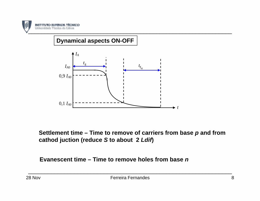
______________________________________________________________
IA
t
Dynamical aspects ON-OFF
IA0
0,9 IA0
stntt
0,1 IA0t
Settlement time – Time to remove of carriers from base p and from th d j ti ( d S t b t 2 Ldif)cathod juction (reduce S to about 2 Ldif)
Evanescent time – Time to remove holes from base n
______________________________________________________________8Ferreira Fernandes28 Nov
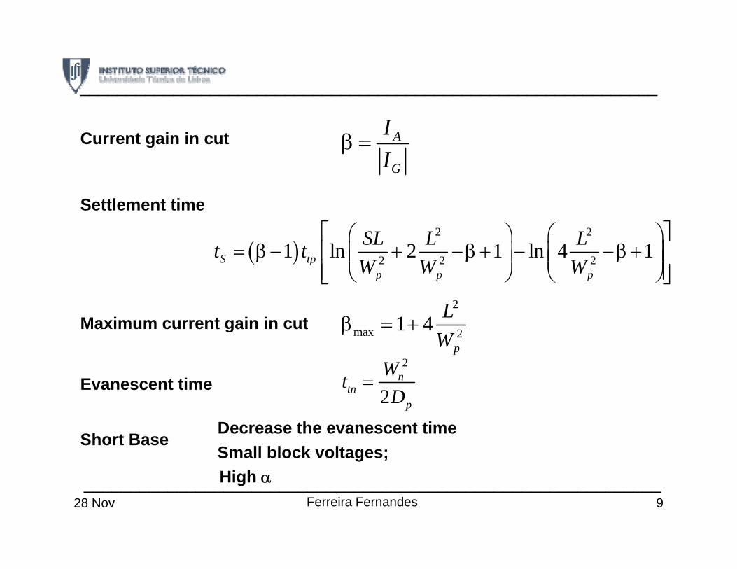
______________________________________________________________
A
G
II
β =Current gain in cut
( )2 2
1 ln 2 1 ln 4 1SL L Lt t⎡ ⎤⎛ ⎞ ⎛ ⎞
β + β+ β+⎢ ⎥⎜ ⎟ ⎜ ⎟
Settlement time
( ) 2 2 21 ln 2 1 ln 4 1S tpp p p
t tW W W
= β− + −β+ − −β+⎢ ⎥⎜ ⎟ ⎜ ⎟⎜ ⎟ ⎜ ⎟⎢ ⎥⎝ ⎠ ⎝ ⎠⎣ ⎦2
1 4 Lβ +Maximum current gain in cut max 21 4
pWβ = +
2
2n
tnWtD
=
Maximum current gain in cut
Evanescent time2tn
pD
Short Base Decrease the evanescent time Small block voltages; High α______________________________________________________________
9Ferreira Fernandes28 Nov
______________________________________________________________
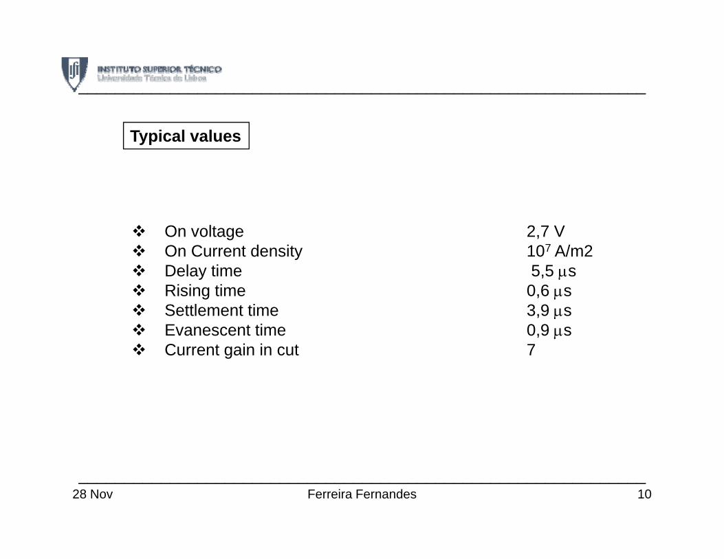
Typical values
On voltage 2,7 V7On Current density 107 A/m2
Delay time 5,5 μsRising time 0,6 μsSettlement time 3,9 μsSettlement time 3,9 μsEvanescent time 0,9 μsCurrent gain in cut 7
______________________________________________________________10Ferreira Fernandes28 Nov
3 Dez 1Ferreira Fernandes
______________________________________________________________
Summary:Compound SemicondutorsCompound Semicondutors
……………………………………………………………………………................…
BinaryBinaryCompound Semicondutors Ternary
Quaternary
III–V – GaAsBinarySemicondutors II–VI – ZnO
IV–VI – PbS
Ex: Famíly III-VGroup III – Al, Ga, InGroup V P As SbGroup V – P, As, Sb
______________________________________________________________2Ferreira Fernandes3 Dez
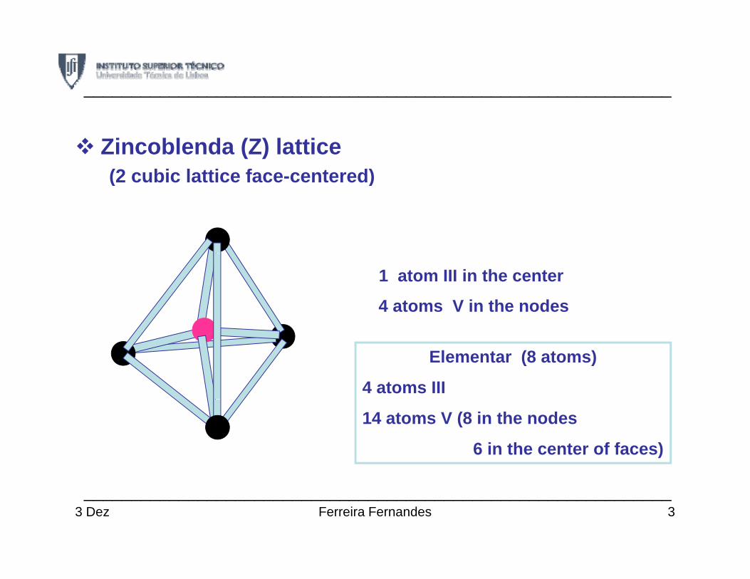
______________________________________________________________
Zincoblenda (Z) lattice(2 cubic lattice face-centered)(2 cubic lattice face centered)
1 atom III in the center
4 atoms V in the nodes
Elementar (8 atoms)
4 atoms III
14 atoms V (8 in the nodes
6 in the center of faces)
3Ferreira Fernandes______________________________________________________________
3 Dez
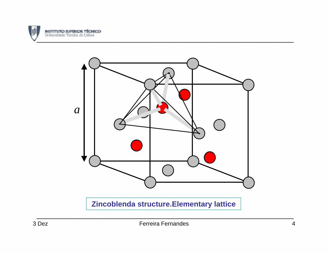
______________________________________________________________
aa
Zincoblenda structure.Elementary latticeZincoblenda structure.Elementary lattice
4Ferreira Fernandes______________________________________________________________
3 Dez
______________________________________________________________
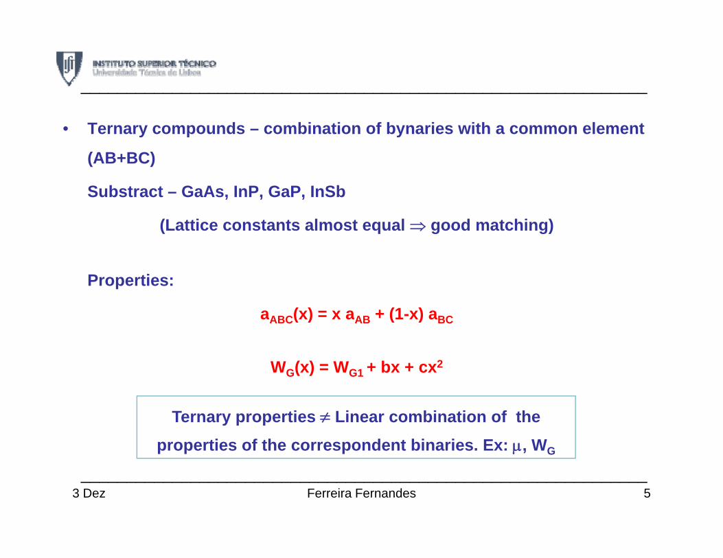
• Ternary compounds – combination of bynaries with a common element
(AB+BC)
Substract – GaAs, InP, GaP, InSb
(Lattice constants almost equal ⇒ good matching)
Properties:
a (x) = x a + (1-x) aaABC(x) = x aAB + (1-x) aBC
WG(x) = WG1 + bx + cx2
Ternary properties ≠ Linear combination of the properties of the correspondent binaries. Ex: μ, WG
5Ferreira Fernandes______________________________________________________________
3 Dez
______________________________________________________________
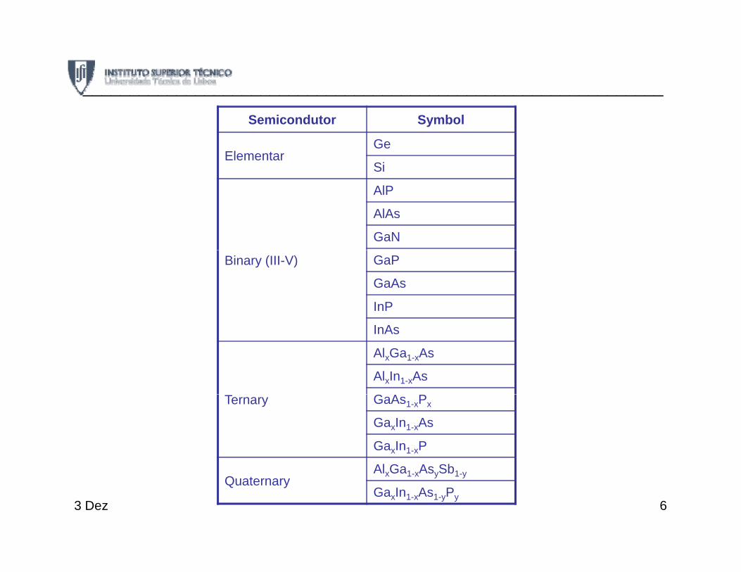
Semicondutor Symbol
ElementarGe
Si
AlP
AlAs
GaN
Binary (III-V) GaP
GaAs
InP
InAs
AlxGa1-xAs
AlxIn1-xAs
GTernary GaAs1-xPx
GaxIn1-xAs
GaxIn1-xP
Al Ga As SbQuaternary
AlxGa1-xAsySb1-y
GaxIn1-xAs1-yPy63 Dez
______________________________________________________________
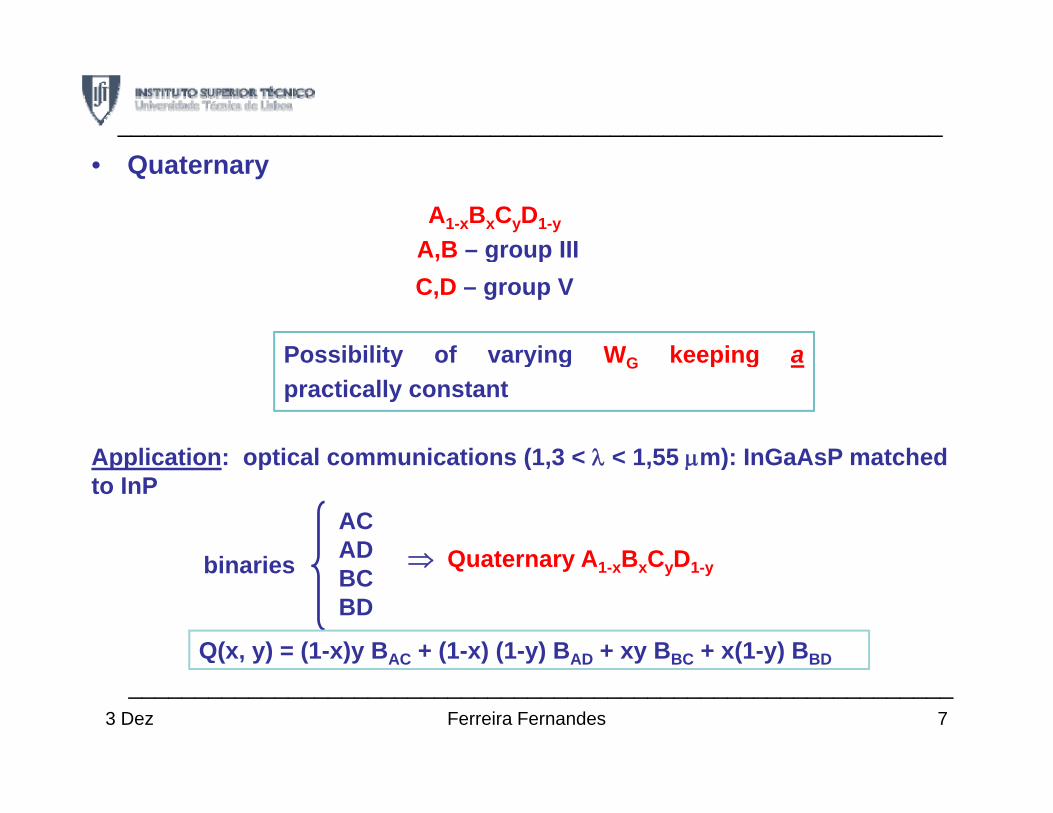
• Quaternary
A1-xBxCyD1-y
A B – group IIIA,B group IIIC,D – group V
Possibility of varying W keeping aPossibility of varying WG keeping apractically constant
Application: optical communications (1 3 < λ < 1 55 μm): InGaAsP matchedApplication: optical communications (1,3 < λ < 1,55 μm): InGaAsP matched to InP
binaries
ACAD ⇒ Quaternary A B C Dbinaries BCBD
⇒ Quaternary A1-xBxCyD1-y
Q(x, y) = (1-x)y BAC + (1-x) (1-y) BAD + xy BBC + x(1-y) BBD( y) ( )y AC ( ) ( y) AD y BC ( y) BD
______________________________________________________________7Ferreira Fernandes3 Dez
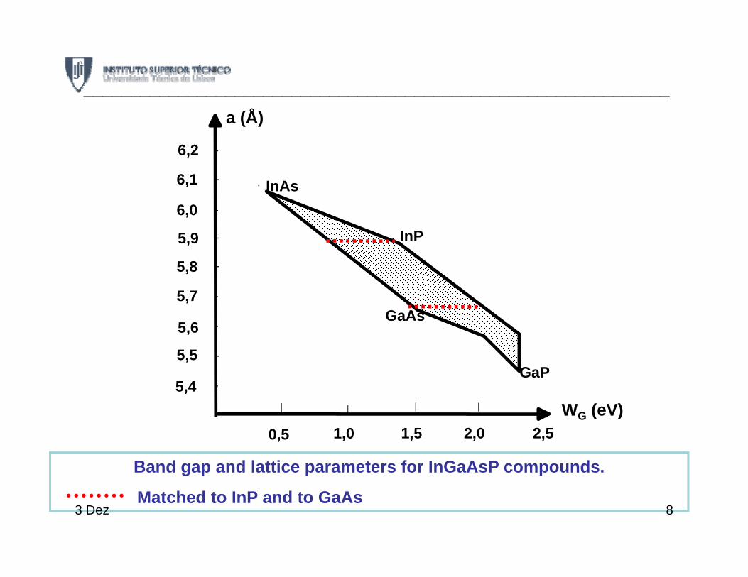
______________________________________________________________
6 1
6,2
a (Å)
-
- .
.
InAs
InP5,9
6,1
6,0
-
-
-
.
GaAs5 6
5,7
5,8 -
-
.
.
GaP5,4
5,5
5,6 -
-
-
Band gap and lattice parameters for InGaAsP compounds.
0,5 1,0 1,5 2,0 2,5WG (eV)| | | |
Band gap and lattice parameters for InGaAsP compounds.
Matched to InP and to GaAs83 Dez

3 Dec
______________________________________________________________
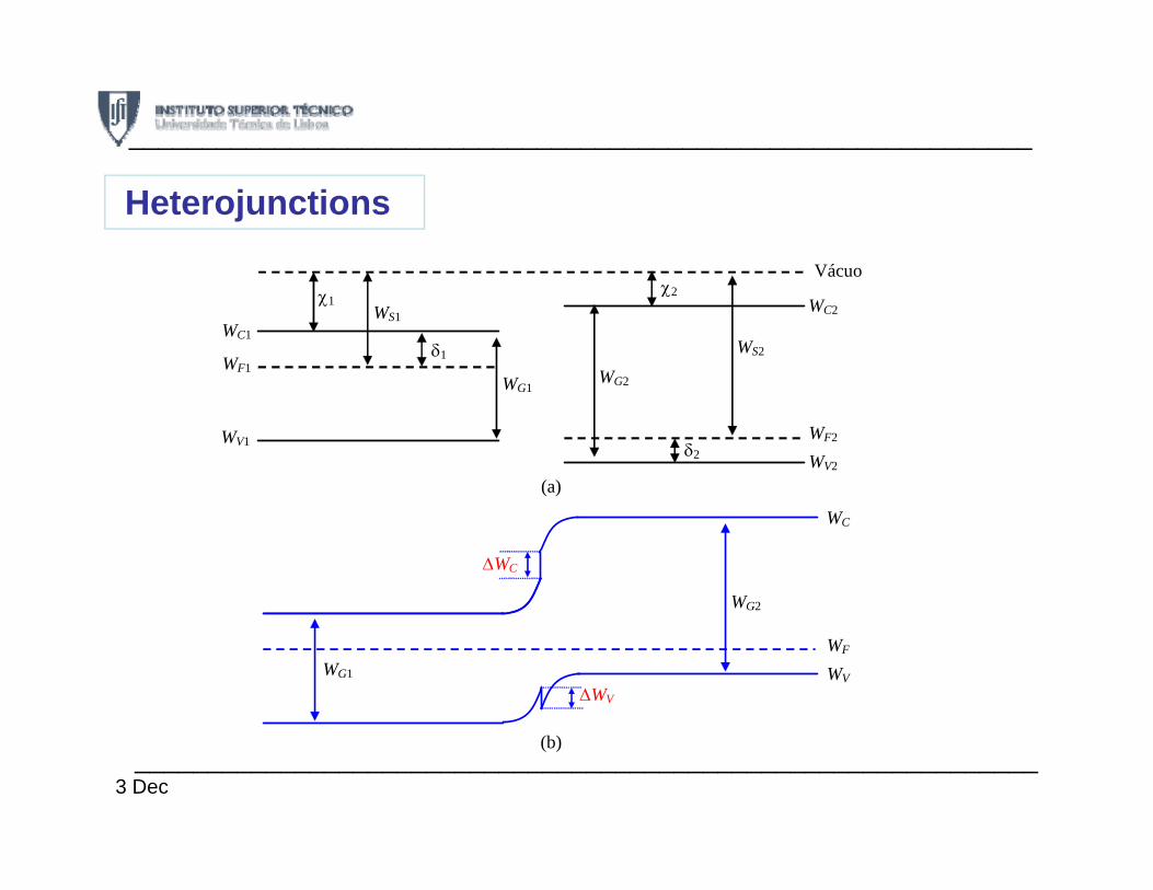
Heterojunctions
Vácuo
WC1 WC2
WF1
χ1 WS1
χ2
WS2 δ1
WG1WG2
WF2 WV1 WV2
δ2
WG1
(a)
WC
WG2
ΔWC
WF WV WG1
ΔWV
(b) ______________________________________________________________
3 Dec

WΔ 1 2CWΔ = χ −χ 2 1C V G GW W W WΔ + Δ = −
( ) ( ) WWWWWWWWV SSVGCGFF
C2112112221
0−
=−−Δ+
=−+Δ−
=−
=δδδδ
W WWG2
qqqqC0
1 20
S SC
W WV
q−
= WG1 WG1 WG2
(a) (b) 21 SS WW =
21 χχ > 0>Δ CW
WG1
WG2
WG1 WG2
GWΔ>− 21 χχ .0<Δ VW
(c) (d) 3 Dec
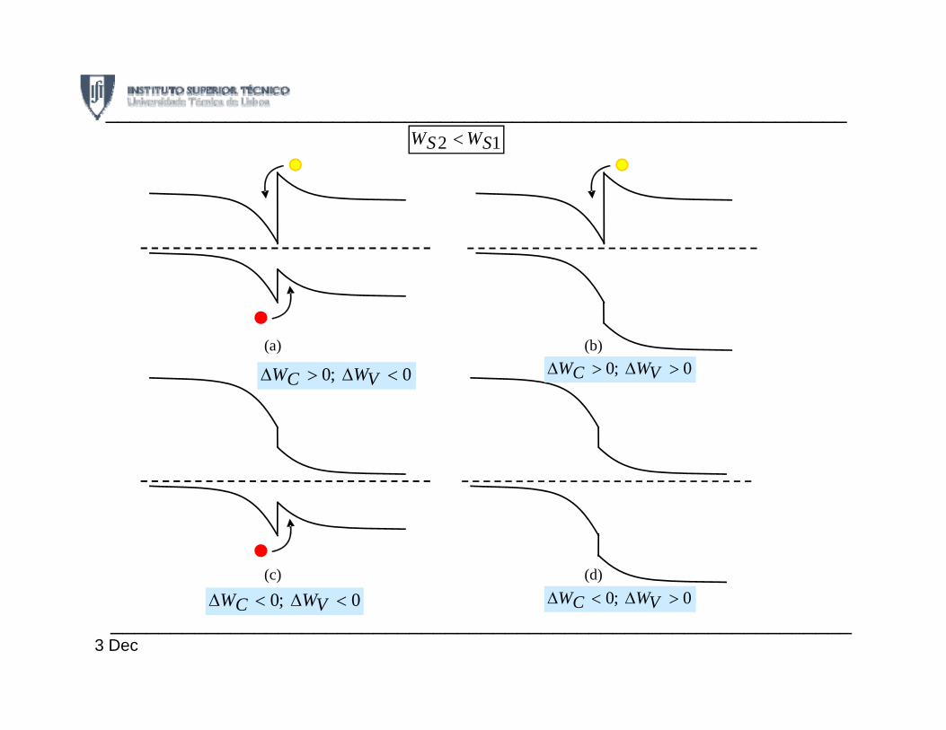
WW <______________________________________________________________
12 SWSW <
(a) (b)
0;0 <Δ>Δ VWCW 0;0 >Δ>Δ VWCW
(c) (d)
00 ΔΔ WW 00 >Δ<Δ WW0;0 <Δ<Δ VWCW 0;0 >Δ<Δ VWCW______________________________________________________________
3 Dec
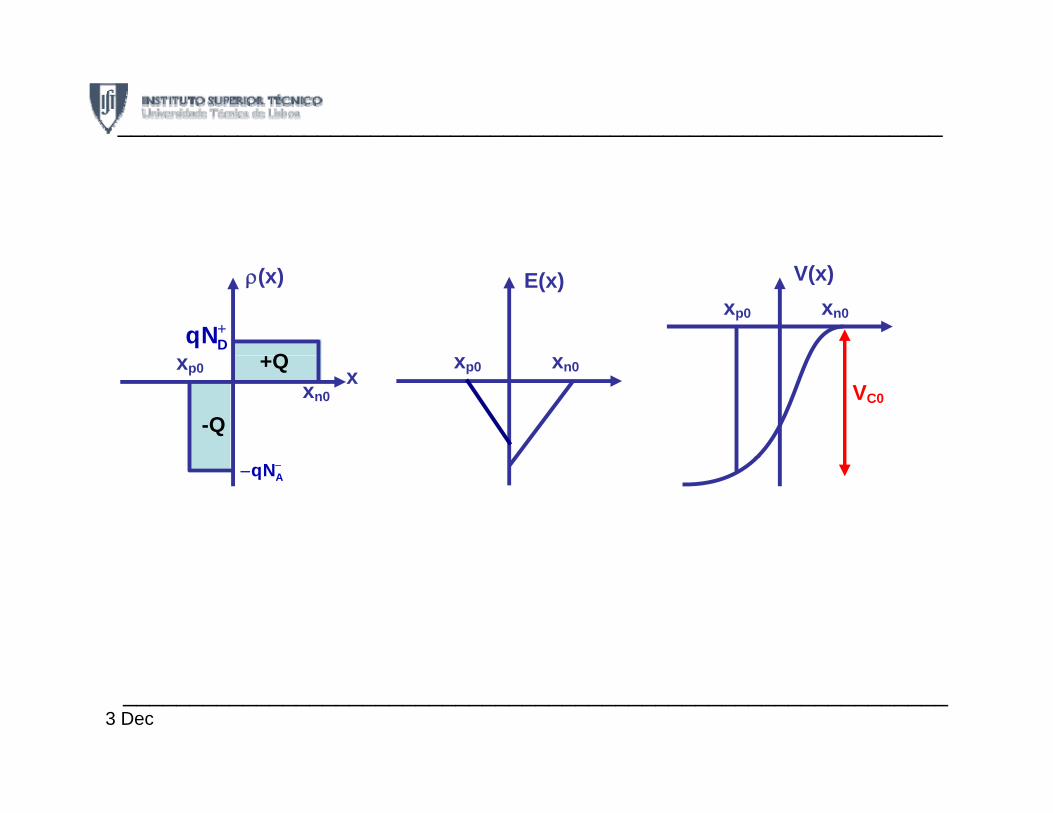
______________________________________________________________
E(x)
xp0 xn0
V(x) ρ(x)
DqN+
Q xp0 xn0
VC0 x
xp0
xn0
+Q
-Q
AqN−−
______________________________________________________________3 Dec
______________________________________________________________
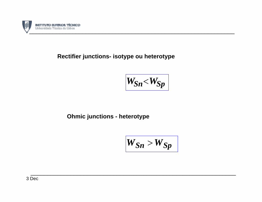
Rectifier junctions- isotype ou heterotype
SpSn WW <
WW
Ohmic junctions - heterotype
SpSn WW >
______________________________________________________________3 Dec
______________________________________________________________
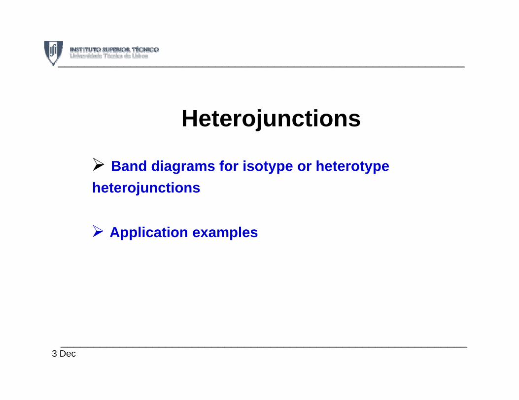
HeterojunctionsHeterojunctions
Band diagrams for isotype or heterotypeheterojunctions
Application examples
______________________________________________________________3 Dec
______________________________________________________________
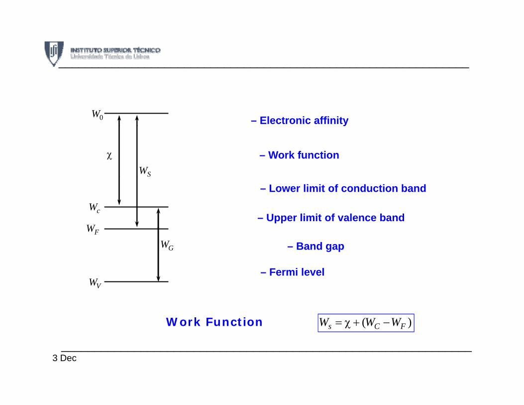
0W – Electronic affinity
χ
SW
y
– Work function
cW
W
– Lower limit of conduction band
– Upper limit of valence bandFW
W
GW – Band gap
– Fermi level
VW
Work Function ( )s C FW W W= χ + −
______________________________________________________________3 Dec
______________________________________________________________
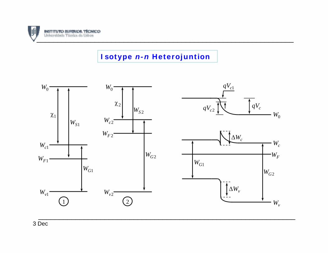
Isotype n-n Heterojuntion
0W 0W
2χ2SW 2cqV
1cqV
cqV1χ
1SW 2cW
2FW
2SW 2cq0W
WcWΔ1cW
1FW
1GW
2GW FW1GW
2GW
cW
1vW 2vW1 2
2G
vW
vWΔ
v
______________________________________________________________3 Dec
______________________________________________________________
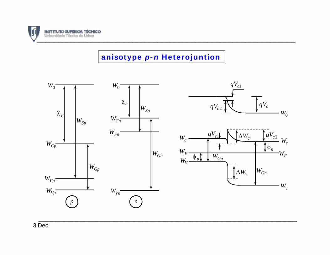
anisotype p-n Heterojuntion
0W
χ
0W
nχSnW 2cqV
1cqV
cqVW
W
pχ SpW CnW
FnW
Sn0W
cWcWΔ 2cqV1cqVcW
CpW
GpW
GnW FWGpW
GnW
c
vWΔ
pφ nφ
FW
VW
FpW
VpW VnWp n
vW
______________________________________________________________3 Dec
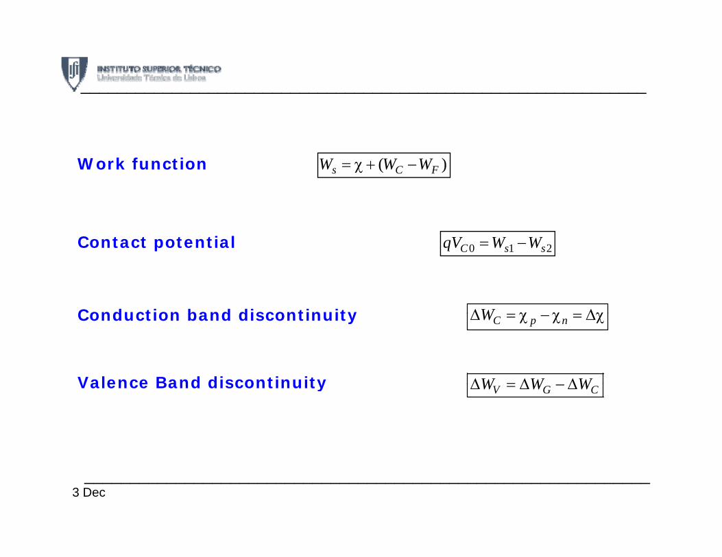
______________________________________________________________
Work function ( )s C FW W W= χ + −
qV W W= −Contact potential
s C F
0 1 2C s sqV W W= −Contact potential
WΔ = χ χ = ΔχConduction band discontinuity C p nWΔ = χ −χ = ΔχConduction band discontinuity
Valence Band discontinuity W W WΔ = Δ ΔValence Band discontinuity V G CW W WΔ = Δ −Δ
______________________________________________________________3 Dec
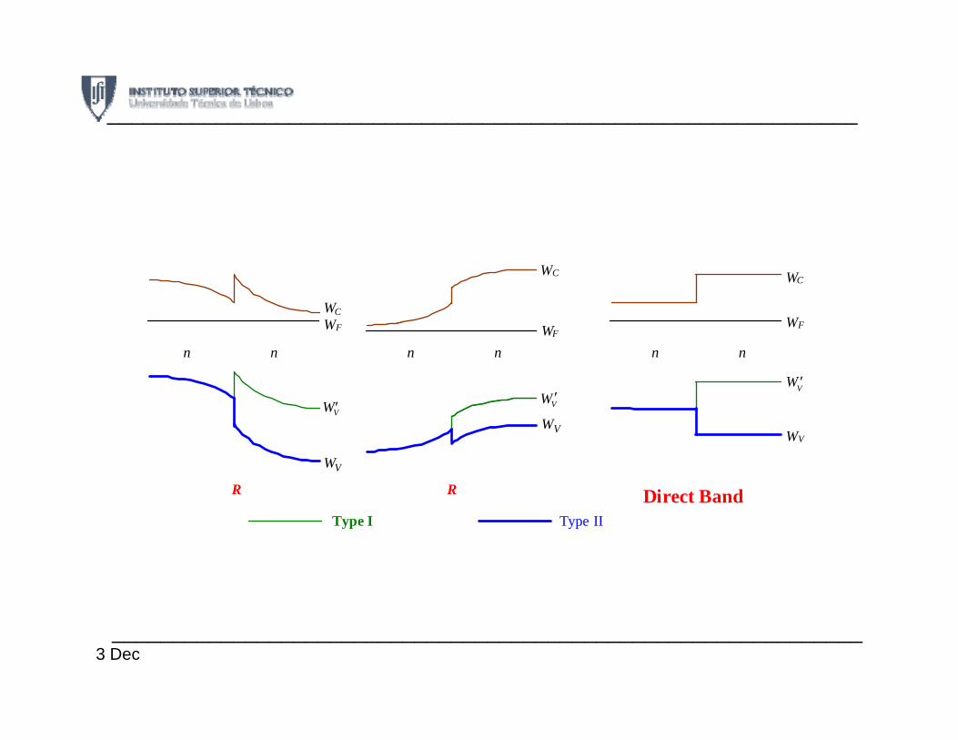
______________________________________________________________
WC W
WC WC
WFWF WF n n n n
VW ′ VW ′
WF
n n
VW ′
WV
WV WV
R R Direct BandType I Type II
______________________________________________________________3 Dec
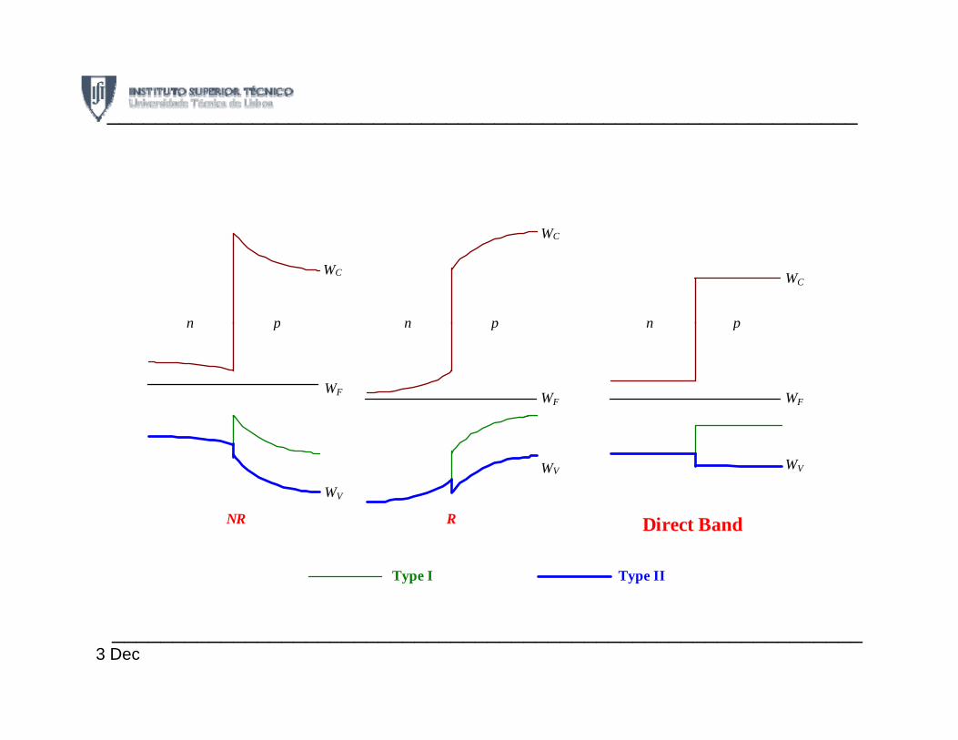
______________________________________________________________
W
WC
WC
WC
n p n p n p
WF WF
WF
n p n p n p
WV
WV
WV
NR R Direct Band
Type I Type II
______________________________________________________________3 Dec
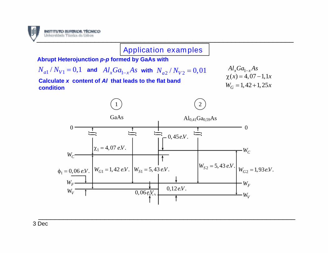
l l
______________________________________________________________Application examples
Abrupt Heterojunction p-p formed by GaAs with
1 1/ 0,1a VN N = and 1x xAl Ga As− with 2 2/ 0,01a VN N =C l l t t t f Al th t l d t th fl t b d
1x xAl Ga As−( ) 4,07 1,1x xχ = −
Calculate x content of Al that leads to the flat band condition
( ) , ,χ1,42 1,25GW x= +
1 2
0
GaAs
0, 45 . .eV0
Al0,41Ga0,59As
∫∫ ∫∫ ∫∫ ∫∫
2 1,93 . .GW eV=
CW1 4,07 . .eVχ =
1 1,42 . .GW eV=1 0,06 . .eVφ = 1 5, 43 . .SW eV=
CW
2 5, 43 . .SW eV=
FW
VW FW
VW0,12 . .eV
0,06 . .eV
______________________________________________________________3 Dec
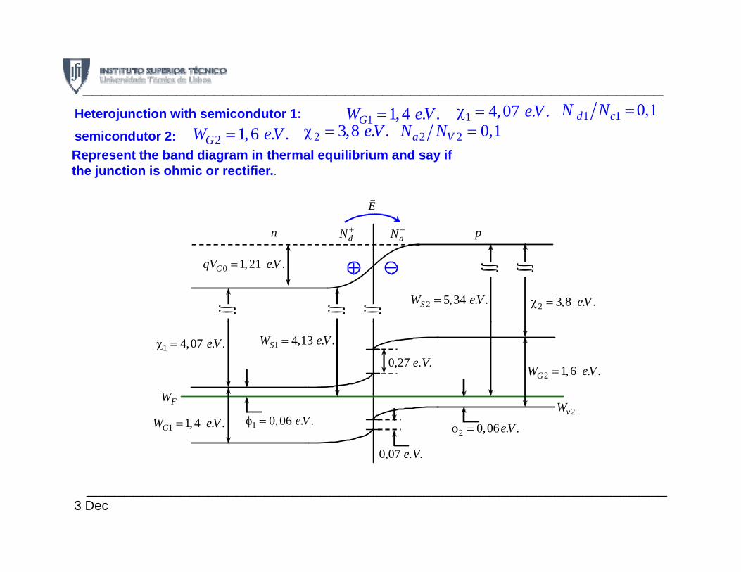
4 07 V 0 1N N______________________________________________________________
Heterojunction with semicondutor 1: 1 1,4 . .GW eV= 1 4,07 . .eVχ = 1 1 0,1d cN N =semicondutor 2: 2 1,6 . .GW eV= 2 3,8 . .eVχ = 2 2 0,1a VN N =Represent the band diagram in thermal equilibrium and say if the junction is ohmic or rectifier..
n dN + p aN −
E
2 5,34 . .SW eV= 2 3,8 . .eVχ =
0 1,21 . .CqV eV=
∫∫ ∫∫ ∫∫
∫∫ ∫∫
2 1,6 . .GW eV=
1 4,13 . .SW eV=
0,27 e.V. 1 4,07 . .eVχ =
W2vW
2 0,06 . .eVφ =
0,07 e.V.
1 0,06 . .eVφ =1 1, 4 . .GW eV=
FW
______________________________________________________________3 Dec
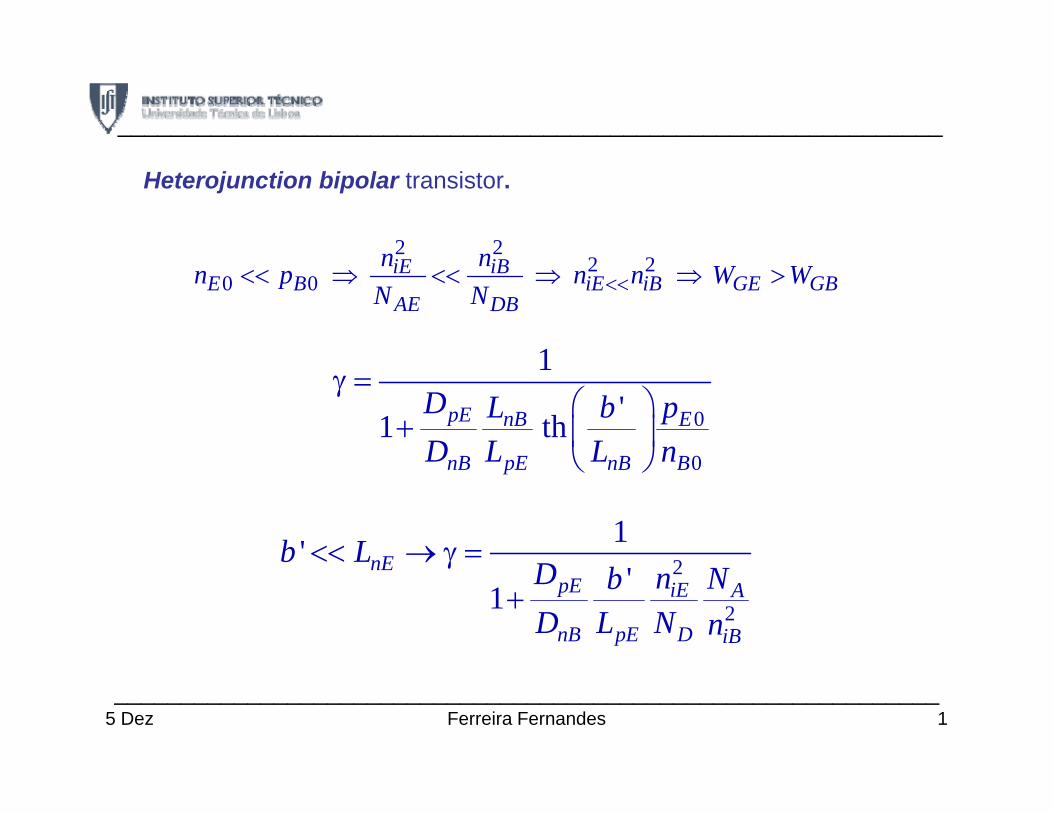
______________________________________________________________
Heterojunction bipolar transistor.
2 22 22 2
0 0iE iB
E B iE iB GE GBAE DB
n nn p n n W WN N <<<< ⇒ << ⇒ ⇒ >
1
0
0
1'1 thpE nB E
B E B B
D L b pD L L n
γ =⎛ ⎞
+ ⎜ ⎟⎝ ⎠ 0nB pE nB BD L L n⎝ ⎠
21' Eb L<< → γ = 2
2'1
nEpE iE A
nB pE D iB
b LD n NbD L N n
<< → γ+
______________________________________________________________1Ferreira Fernandes5 Dez
______________________________________________________________
eBase Colector Base EmissorN N N N> >
Base more doped⇒ smaller b ⇒ θ ~1,
eBase Colector Base EmissorN N N N> >
⇒ Base resistance decreases
Since the transition regions are larger in emitter and collector zonesSince the transition regions are larger in emitter and collector zones
decreases the transition capacities of both junctions.
1iB iEn n>> ⇒ γ ≅ ⇒ α ≅ θ
2Ferreira Fernandes______________________________________________________________
5 Dez
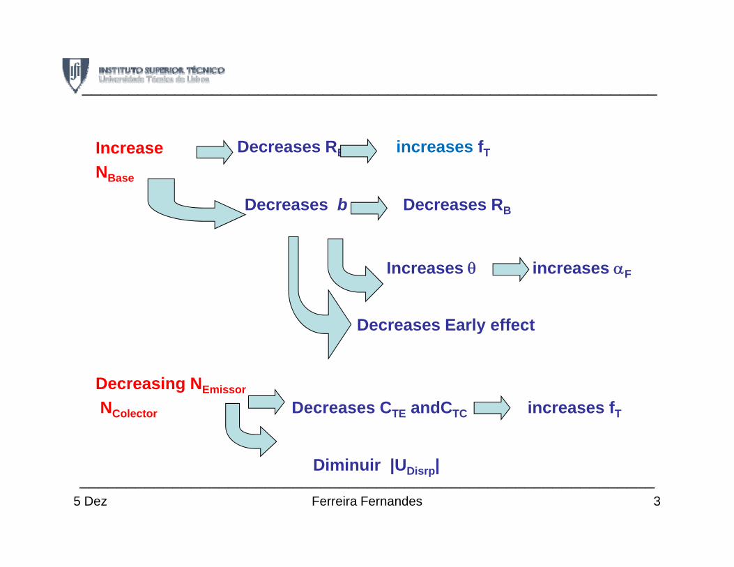
______________________________________________________________
Increase NBase
Decreases RB increases fT
NBase
Decreases b Decreases RB
Increases θ increases αF
D E l ff t
Decreasing NEmissor
Decreases Early effect
g Emissor
NColector Decreases CTE andCTC increases fT
Diminuir |U |Diminuir |UDisrp|
3Ferreira Fernandes______________________________________________________________
5 Dez

1Ferreira Fernandes10 Dec
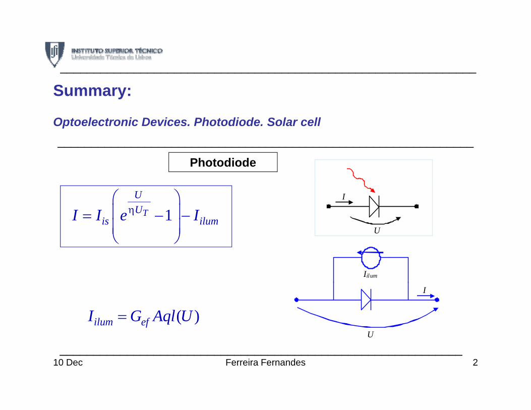
______________________________________________________________
Summary:
Optoelectronic Devices. Photodiode. Solar cellp
Photodiode
______________________________________________________________
1T
UU
is ilumI I e Iη⎛ ⎞⎜ ⎟= − −⎜ ⎟⎝ ⎠
I
U⎜ ⎟⎝ ⎠ U
Iilum
( )ilum efI G Aql U=
I
UU
____________________________________________________________2Ferreira Fernandes10 Dec
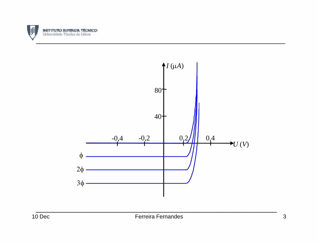
______________________________________________________________
I (μA)
80
0 4 0 2 0 2
40
0 4U (V)
φ
2φ
-0,4 -0,2 0,2 0,4
2φ
3φ
____________________________________________________________3Ferreira Fernandes10 Dec
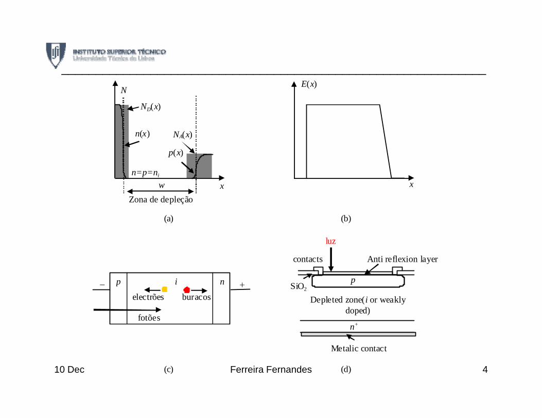
______________________________________________________________ E(x)
N
ND(x)
n(x) NA(x)
p(x)
n=p=ni xxw
Zona de depleção
(a) (b)
p i n − +
contacts Anti reflexion layer
luz
SiO2p
electrões buracos
fotões
SiO2
n+
Depleted zone(i or weakly doped)
Metalic contact
(c) (d) 410 Dec Ferreira Fernandes
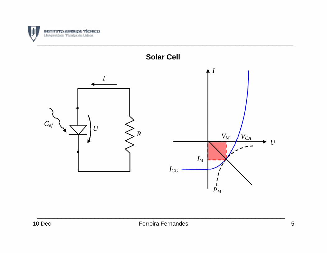
______________________________________________________________
I
I
Solar Cell
I
Gef U
UR VCA VM
U
IM ICC
PM
____________________________________________________________5Ferreira Fernandes10 Dec
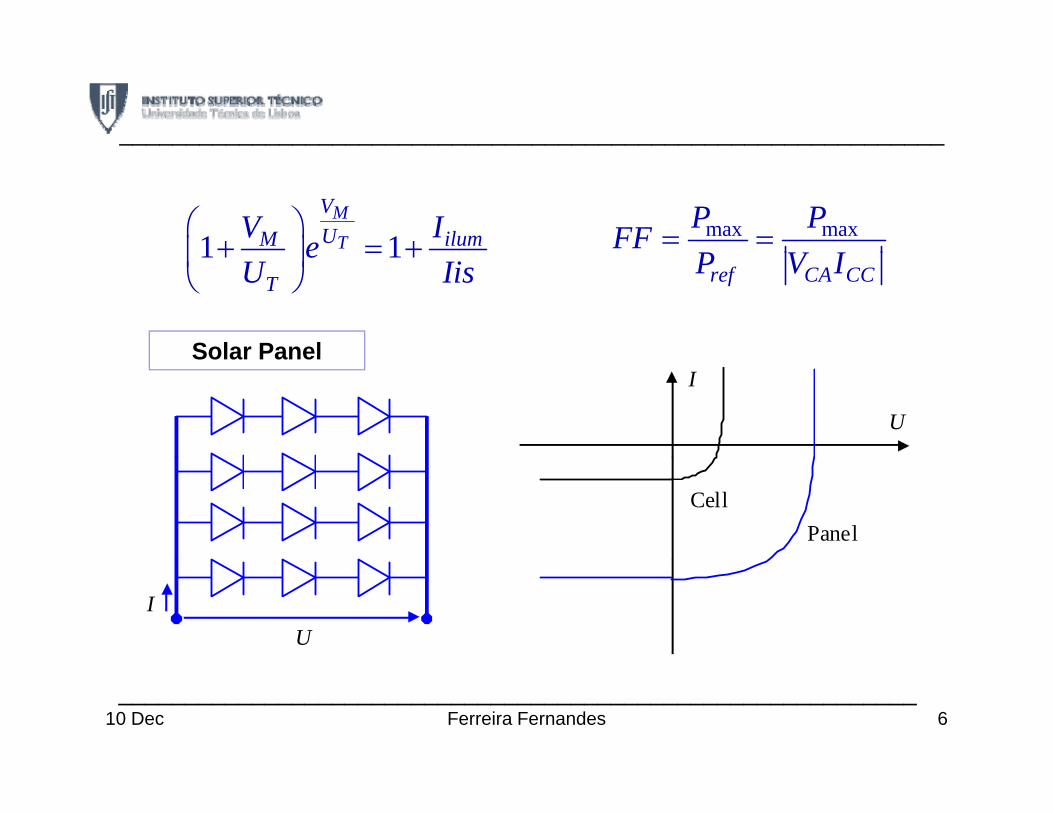
______________________________________________________________
1 1MT
VUM ilumV Ie
⎛ ⎞+ = +⎜ ⎟
max maxP PFFP V I
= =1 1T
eU Iis
+ = +⎜ ⎟⎝ ⎠ ref CA CCP V I
Solar Panel I
U
Solar Panel
Panel Cell
I U
____________________________________________________________6Ferreira Fernandes10 Dec
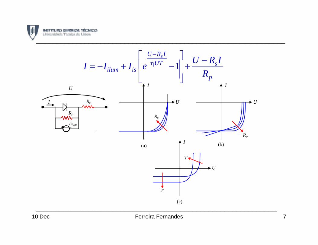
______________________________________________________________
1sU R I
UT silum is
U R II I I eR
−η
⎡ ⎤ −⎢ ⎥= − + − +⎢ ⎥⎣ ⎦ pR⎢ ⎥⎣ ⎦
I
U
I
U I
U
Rs
.
Rs
Rp
Rp
Iilum
I
U
p
T
(a) (b)
U
T
( )(c)____________________________________________________________
7Ferreira Fernandes10 Dec
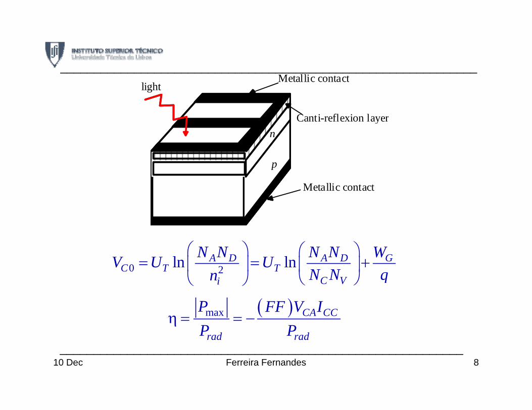
M t lli t t______________________________________________________________
Canti-reflexion layer
Metallic contact
n
light
n
p
n
p
Metallic contact
0 2ln lnA D A D GC T T
C Vi
N N N N WV U UN N qn
⎛ ⎞ ⎛ ⎞= = +⎜ ⎟ ⎜ ⎟
⎝ ⎠⎝ ⎠ C Vi q⎝ ⎠⎝ ⎠
( )max CA CC
d d
P FF V IP P
η = = −rad radP P
____________________________________________________________8Ferreira Fernandes10 Dec
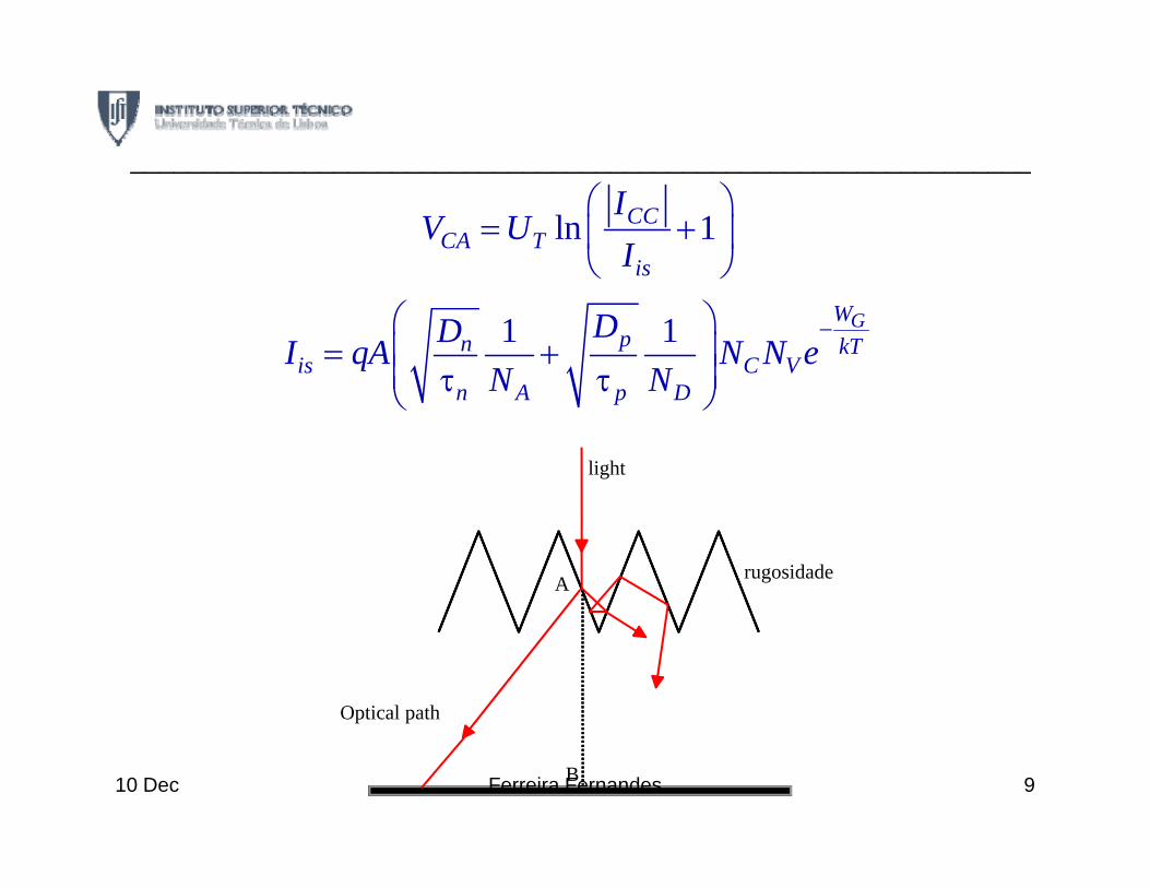
ln 1CCCA T
is
IV U
I⎛ ⎞
= +⎜ ⎟⎝ ⎠
______________________________________________________________
⎝ ⎠
1 1 GWpn kT
is C VA D
DDI qA N N eN N
−⎛ ⎞⎜ ⎟= +⎜ ⎟τ τ⎝ ⎠n A p DN N⎜ ⎟τ τ⎝ ⎠
light
rugosidadeA
Optical path
B 910 Dec Ferreira Fernandes
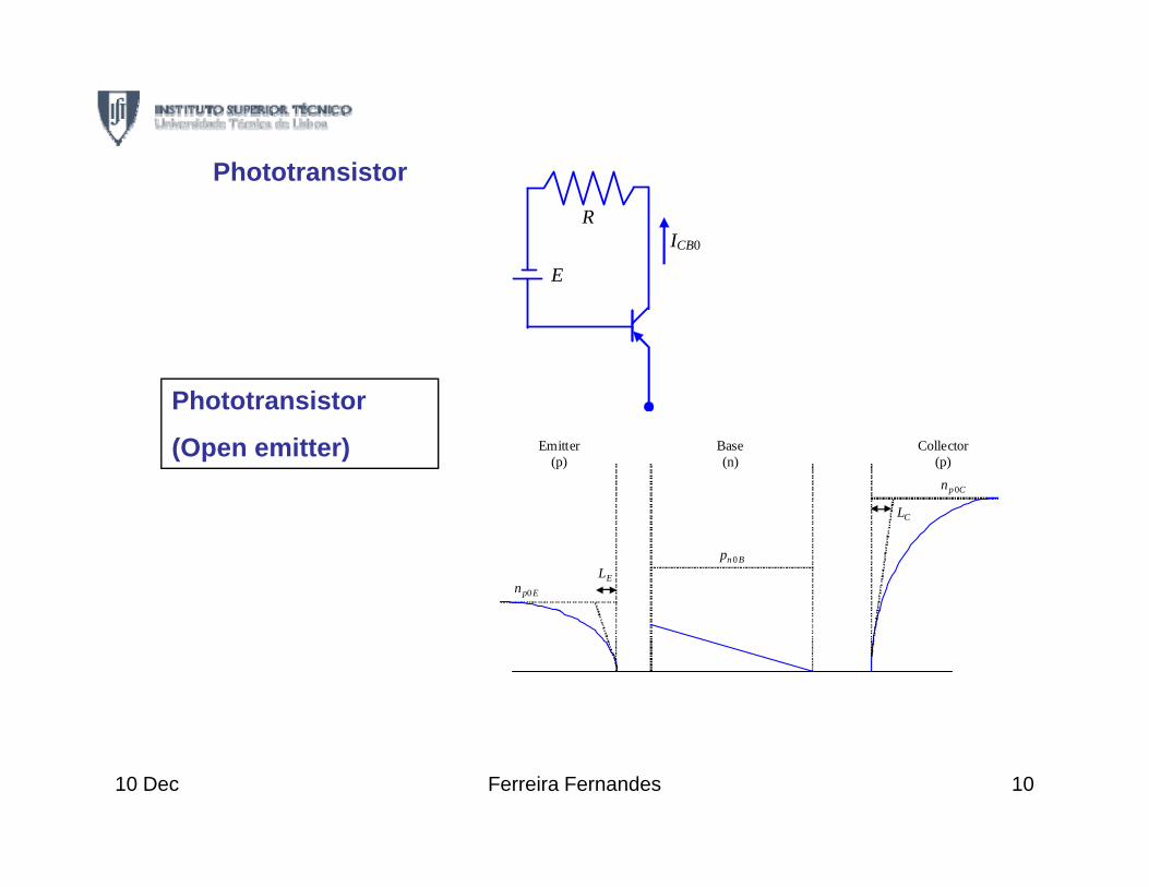
Ph t t i tPhototransistor
R
E
ICB0
E
Emitter (p)
Base (n)
Collector (p)
0p Cn
Phototransistor
(Open emitter)
0p En
0n BpEL
CL
1010 Dec Ferreira Fernandes
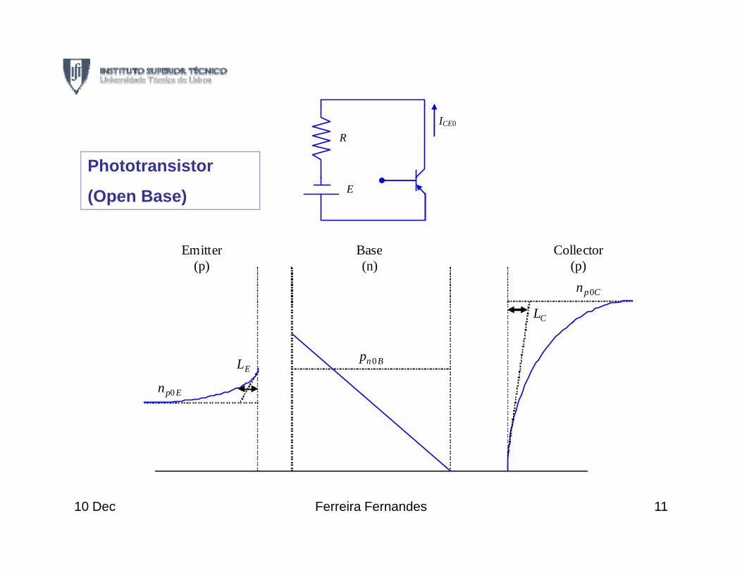
R ICE0
Phototransistor
Emitter Base Collector
E (Open Base)
Emitter (p)
Base(n)
Collector(p)
0p Cn
CL
0p En
0n BpEL
0p E
1110 Dec Ferreira Fernandes
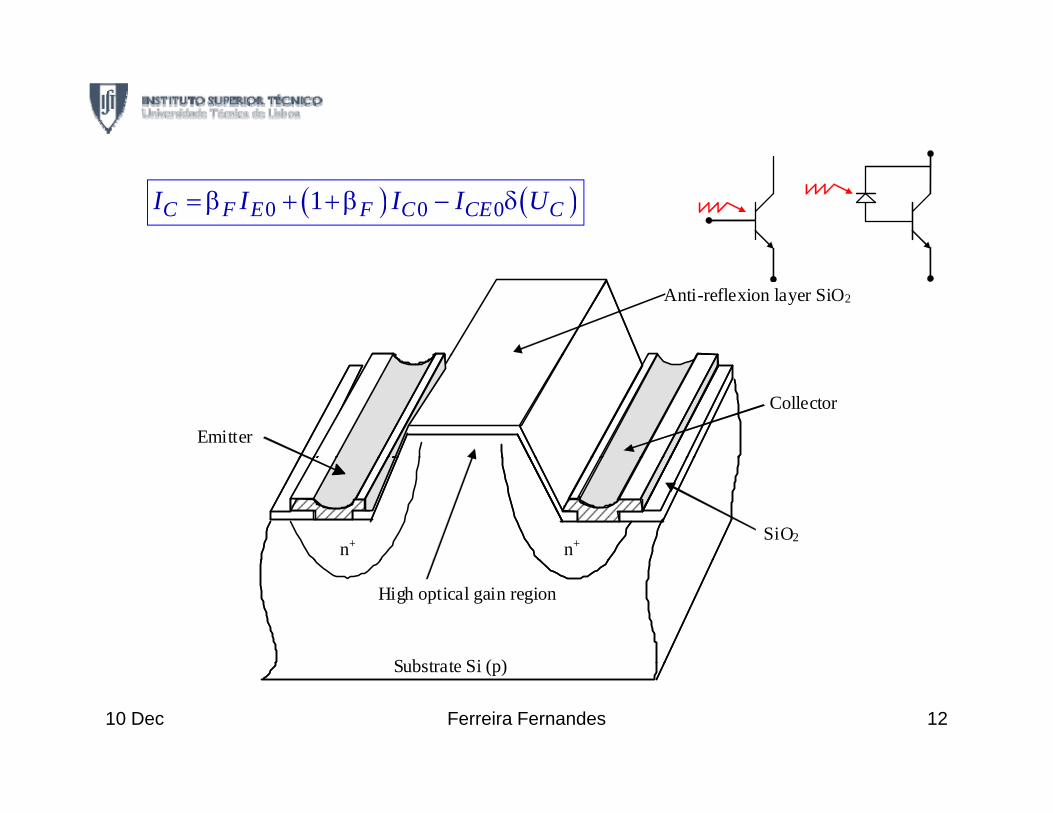
( ) ( )0 0 01C F E F C CE CI I I I U= β + + β − δ
Anti-reflexion layer SiO2
Collector
Emitter
SiO2 n+ n+
High optical gain region
S b t t Si ( )
1210 Dec
Substrate Si (p)
Ferreira Fernandes
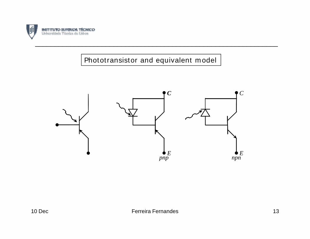
______________________________________________________________
Phototransistor and equivalent model
C C
pnp E
npn E
1310 Dec Ferreira Fernandes
12 Dez Ferreira Fernandes
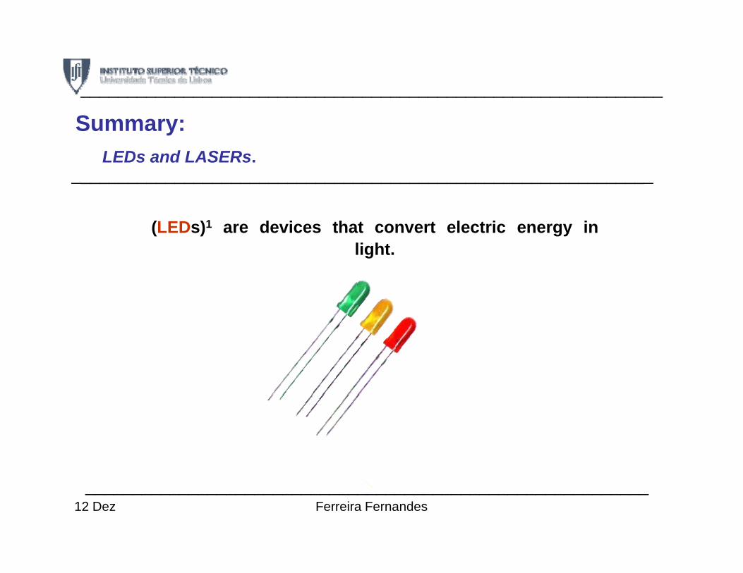
______________________________________________________________
Summary:LEDs and LASERs.
(LEDs)1 are devices that convert electric energy inlight
______________________________________________________________
light.
____________________________________________________________12 Dez Ferreira Fernandes
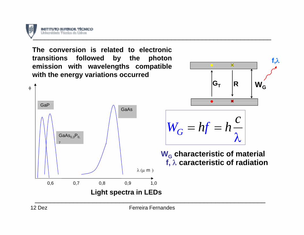
______________________________________________________________
The conversion is related to electronictransitions followed by the photonemission with wavelengths compatible
ith th i ti d
f,λ
with the energy variations occurredGT R WGφ
GaPGaAs
GW f ch h= =GaAs0,3P0,
7
G fλ
WG characteristic of materialf λ caracteristic of radiation
λ (μ )m
0,6 0,7 0,8 0,9 1,0
Light spectra in LEDs
f, λ caracteristic of radiation
Light spectra in LEDs____________________________________________________________
12 Dez Ferreira Fernandes
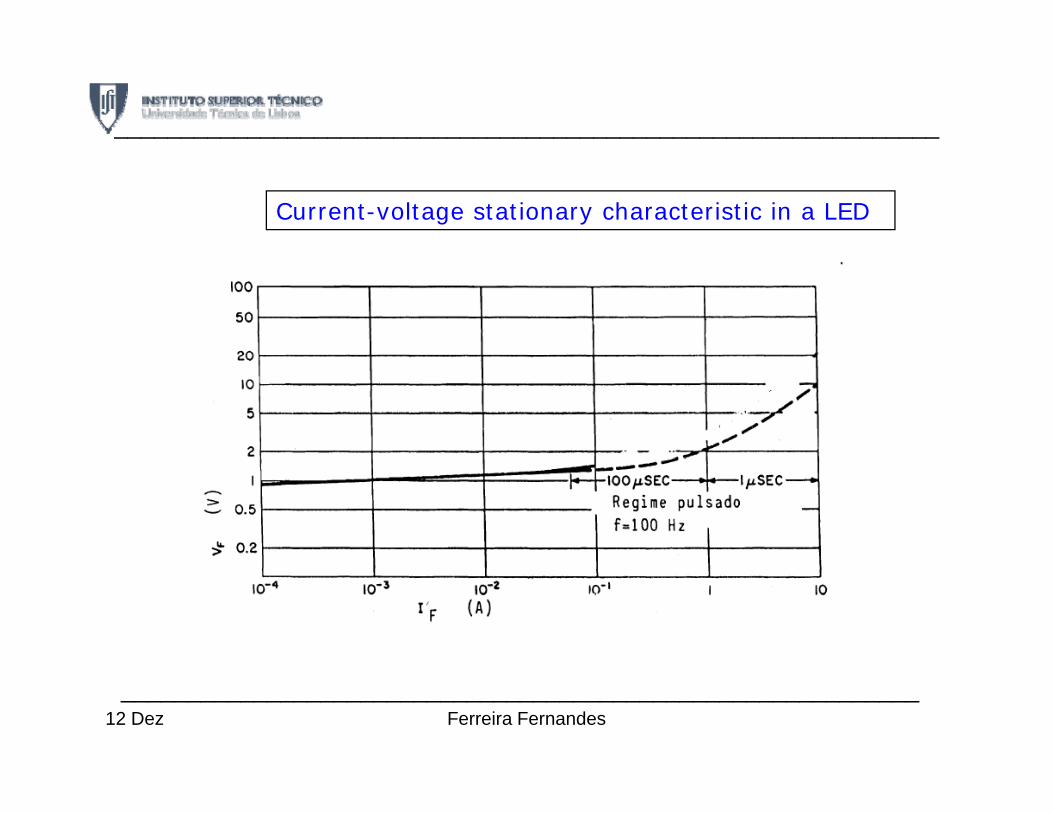
______________________________________________________________
Current-voltage stationary characteristic in a LED
____________________________________________________________12 Dez Ferreira Fernandes
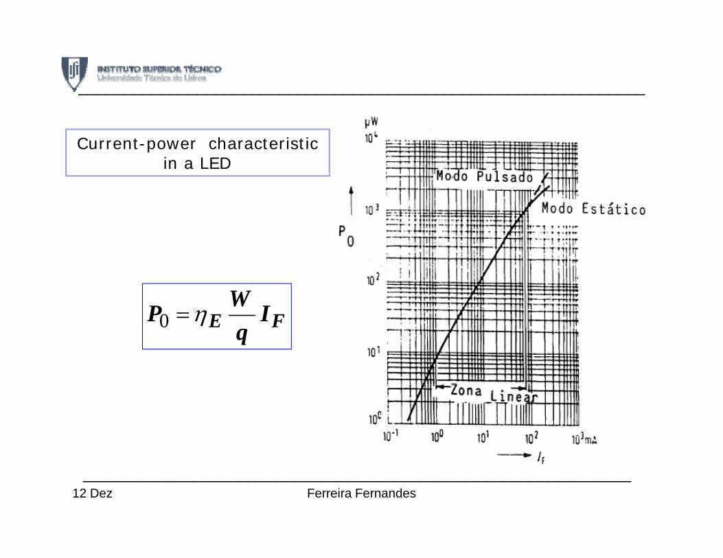
______________________________________________________________
Current-power characteristicin a LED
FE IWP η=0 FE Iq
P η=0
____________________________________________________________12 Dez Ferreira Fernandes
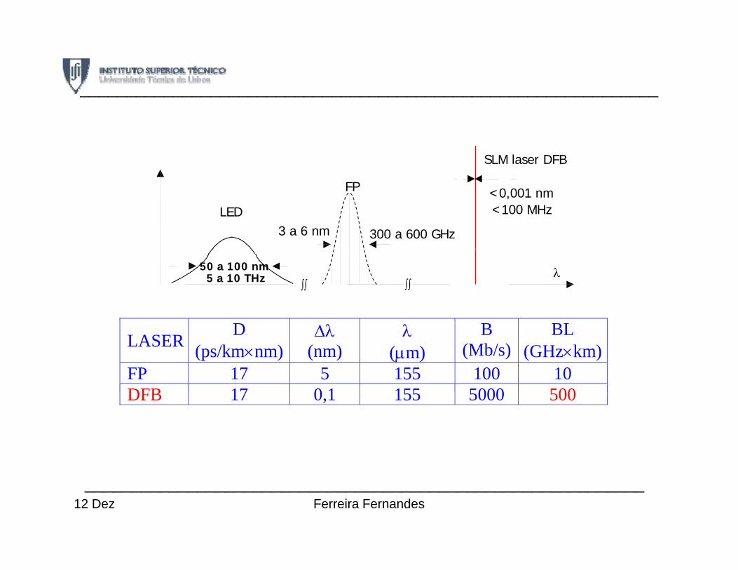
______________________________________________________________
SLM laser DFB
3 a 6 nm 300 a 600 GHz
LED
FP <0,001 nm<100 MHz
50 a 100 nm5 a 10 THz λ
ÚÚ ÚÚ
LASER D(ps/km×nm)
Δλ (nm)
λ (μm)
B(Mb/s)
BL(GHz×km)
FP 17 5 155 100 10 DFB 17 0 1 155 5000 500DFB 17 0,1 155 5000 500
____________________________________________________________12 Dez Ferreira Fernandes
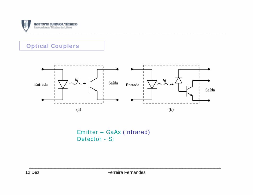
______________________________________________________________
Optical Couplers
Entrada Saídahf
Entradahf
Entrada EntradaSaída
(a) (b)(a) (b)
Emitter – GaAs (infrared)( )Detector - Si
____________________________________________________________12 Dez Ferreira Fernandes
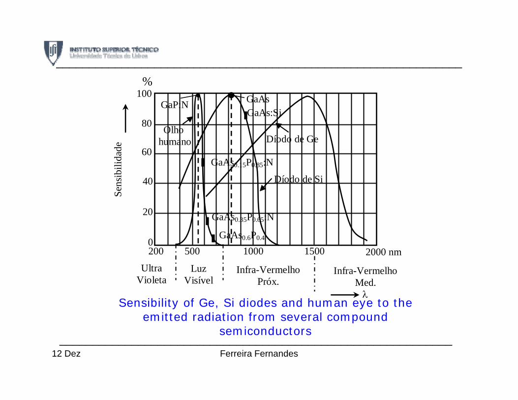
______________________________________________________________ %
100
80
GaP:N GaAs GaAs:Si
80
60 GaAs0.15P0.85:N
Díodo de Ge
bilid
ade
Olho humano
40
20
Díodo de Si
GaAs0.35P0.65:N
Sens
ib
0 200 500 1000 1500 2000 nm
Ultra Luz Infra-Vermelho Infra-Vermelho
GaAs0.6P0.4
Violeta Visível Próx. Med. λ
Sensibility of Ge, Si diodes and human eye to the emitted radiation from several compound
dsemiconductors____________________________________________________________
12 Dez Ferreira Fernandes
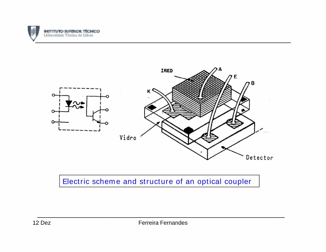
______________________________________________________________
Electric scheme and structure of an optical coupler
____________________________________________________________12 Dez Ferreira Fernandes
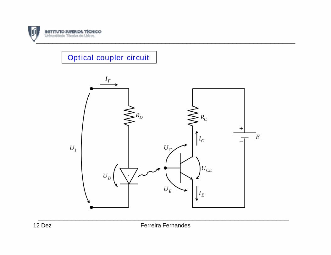
______________________________________________________________
I
Optical coupler circuit
FI
DRCR
CI
+
− E
U
1U
CEU
CU
DU
EIEU
____________________________________________________________12 Dez Ferreira Fernandes
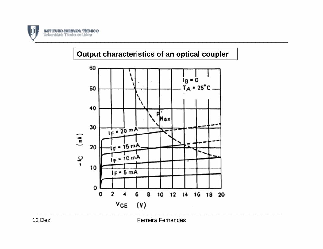
______________________________________________________________
Output characteristics of an optical coupler
____________________________________________________________12 Dez Ferreira Fernandes
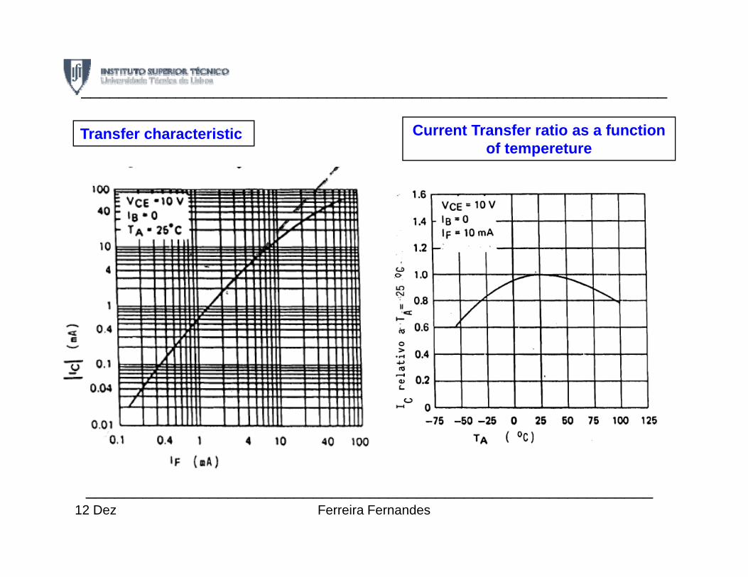
______________________________________________________________
Transfer characteristic Current Transfer ratio as a function of tempereture
____________________________________________________________12 Dez Ferreira Fernandes
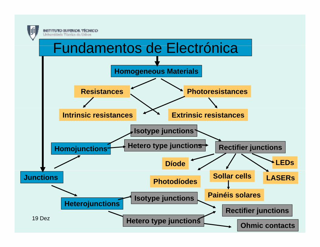
Fundamentos de ElectrónicaHomogeneous Materials
Fundamentos de Electrónica
Resistances Photoresistances
Intrinsic resistances Extrinsic resistances
Isotype junctions
Hetero type junctions Rectifier junctions
Díode
Homojunctions
LEDs
Junctions
H t j ti
PhotodíodesSollar cells
Painéis solares
LASERs
Isotype junctions
19 DezOhmic contacts
HeterojunctionsRectifier junctions
yp j
Hetero type junctions
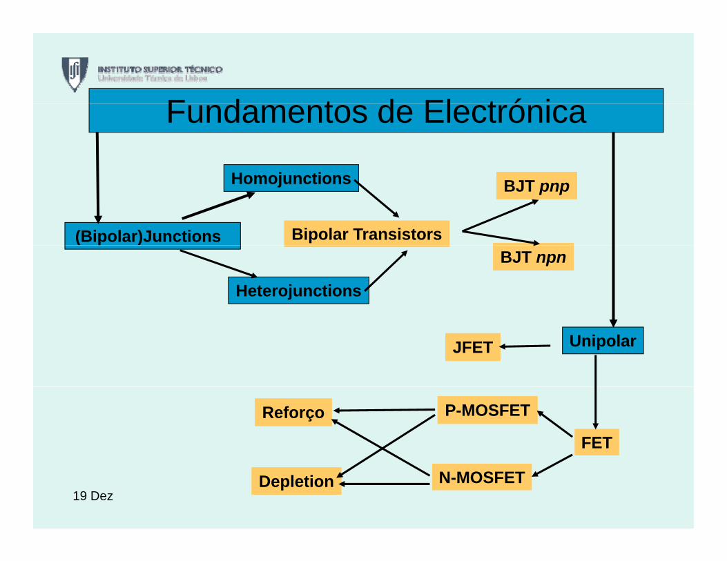
F d t d El t ó i
H j ti
Fundamentos de Electrónica
(Bipolar)Junctions Bipolar Transistors
BJT pnpHomojunctions
( )
Heterojunctions
BJT npn
UnipolarJFET
FET
Reforço P-MOSFET
19 DezN-MOSFETDepletion
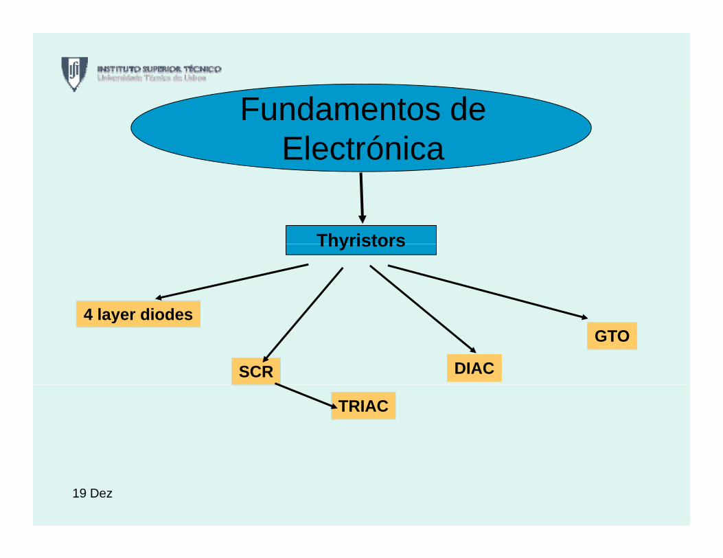
Fundamentos deFundamentos de Electrónica
Thyristors
4 layer diodes
Thyristors
4 layer diodesGTO
SCR DIAC
TRIAC
19 Dez
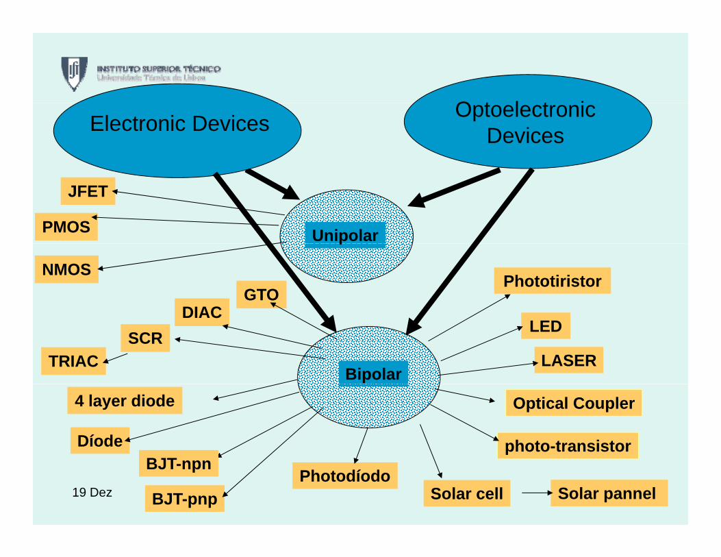
O t l t iElectronic Devices Optoelectronic Devices
UnipolarPMOS
JFET
p
GTODIAC
NMOSPhototiristor
Bipolar
SCRDIAC
TRIAC
LED
LASER
4 layer diode
Díode photo-transistor
Optical Coupler
19 DezPhotodíodo
Solar cell
BJT-npn
BJT-pnp
p
Solar pannel