functional electrical stimulation by nanogenerator with 58 v … · 2012-05-21 · functional...
TRANSCRIPT

Functional Electrical Stimulation by Nanogenerator with 58 V OutputVoltageGuang Zhu,† Aurelia C. Wang,† Ying Liu,† Yusheng Zhou,† and Zhong Lin Wang*,†,‡
†School of Materials Science and Engineering, Georgia Institute of Technology, Atlanta, Georgia 30332-0245, United States‡Beijing Institute of Nanoenergy and Nanosystems, Chinese Academy of Sciences, Beijing, China
*S Supporting Information
ABSTRACT: We demonstrate a new type of integrated nano-generator based on arrays of vertically aligned piezoelectric ZnOnanowires. The peak open-circuit voltage and short-circuit currentreach a record high level of 58 V and 134 μA, respectively, with amaximum power density of 0.78 W/cm3. The electric output wasdirectly applied to a sciatic nerve of a frog, inducing innervation ofthe nerve. Vibrant contraction of the frog’s gastrocnemius muscleis observed as a result of the instantaneous electric input from thenanogenerator.
KEYWORDS: Nanogenerator, ZnO, energy harvesting, functional electrical stimulation
The modern life is inexorably dependent on emergingtechnologies in stand-alone portable systems designed to
provide complete and personal solutions.1 Integration of micro-to-nanosized sensors, actuators/transducers, and medical im-plants leads to ultraminiaturized and multifunctional smartsystems that are expected to provide unprecedented life qualityfor human kinds.2−4 For such a system that consumes muchless power than do their bulky counterparts, it is not onlysignificant but also very feasible to harvest ambient energy tobuild self-powered systems that can operate independently andsustainably. Here, we achieved real-time functional electricalstimulation (FES) of a sciatic nerve of a frog by a new type ofZnO-nanowire (NW)-based nanogenerator (NG) that pro-duced electricity from biomechanical energy. The electricoutput from the NG reached a record high of 58 V and 134 μA,with a maximum power density of 0.78 W/cm3. It was sufficientto directly and instantaneously induce innervating of the motornever and hence contraction of the frog’s gastrocnemiusmuscle. Our demonstration suggests potential applications ofthe nanogenerator in biomedical and neurological fields, such asthe power source for neuroprosthetic devices.Since 2005, we have been developing “self-powered nano-
technology” by ZnO-nanowire-based NGs.5,6 By virtue of thepiezoelectric effect of ZnO NWs, the NGs target ambientmechanical energy, transforming it into electrical energy. As aresult of worldwide efforts, such a concept is being developedinto a practical technology with a variety of demonstratedapplications.7−13 However, a major limitation was that theoutput power of a NG was still not sufficiently high enough forreal-time operation of conventional electronics.
The previously designed NGs utilized the Schottky barrierbetween metal−semiconductor contacts, which was requiredfor charge accumulation.5,14−16 In this work we developed anovel design and process flow for fabricating an integrated NGbased on position-controlled vertical ZnO NWs. The Schottkycontact was replaced by a thin insulating layer that prevents thecurrent leakage through the internal structure. The process flowfor fabrication is shown in Figure 1. A precleaned siliconsubstrate was consecutively deposited with an ITO layer and aZnO seed layer by RF sputtering (Figure 1a−c). Not only doesthe ITO layer play a role as a conductive electrode, but also itpromotes adhesion between the ZnO seed and the substrate.Photolithography was then performed to open an array ofsquare windows on photoresist with narrow spacing in between(Figure 1d). The photoresist serves as a mask so that ZnONWs only grow on the exposed seed surface in the subsequentsynthesis step by wet mechical method (Figure 1e). Followingstripping off any residual photoresist (Figure 1f), the NWs werethermally annealed. Then a layer of PMMA was applied coverthe synthesized NWs (Figure 1g) by spin-coating, followed bydepositing a top metal electrode of aluminum (Figure 1h).Finally, another layer of PMMA was used for packaging (Figure1i). Two terminal leads rested on the ITO layer and thealuminum layer for electrical measurement. The process flow iscompatible with batch fabrication techniques, which allowmultiple silicon wafers to be parallel processed, followed by
Received: March 11, 2012Revised: May 11, 2012
Letter
pubs.acs.org/NanoLett
© XXXX American Chemical Society A dx.doi.org/10.1021/nl300972f | Nano Lett. XXXX, XXX, XXX−XXX
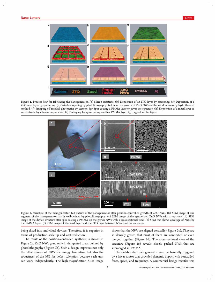
being diced into individual devices. Therefore, it is superior interms of production scale-up and cost reduction.The result of the position-controlled synthesis is shown in
Figure 2a. ZnO NWs grew only in designated areas defined byphotolithography (Figure 2b). Such a design improves not onlythe effectiveness of NWs for energy harvesting but also therobustness of the NG for defect toleration because each unitcan work independently. The high-magnification SEM image
shows that the NWs are aligned vertically (Figure 2c). They areso densely grown that most of them are connected or evenmerged together (Figure 2d). The cross-sectional view of thestructure (Figure 2e) reveals closely packed NWs that aresubmerged in PMMA.The as-fabricated nanogenerator was mechanically triggered
by a linear motor that provided dynamic impact with controlledforce, speed, and frequency. A commercial bridge rectifier was
Figure 1. Process flow for fabricating the nanogenerator. (a) Silicon substrate. (b) Deposition of an ITO layer by sputtering. (c) Deposition of aZnO seed layer by sputtering. (d) Window opening by photolithography. (e) Selective growth of ZnO NWs on the window areas by hydrothermalmethod. (f) Stripping off residual photoresist by acetone. (g) Spin-coating a PMMA layer to cover the structure. (h) Deposition of a metal layer asan electrode by e-beam evaporation. (i) Packaging by spin-coating another PMMA layer. (j) Legend of the figure.
Figure 2. Structure of the nanogenerator. (a) Picture of the nanogenerator after position-controlled growth of ZnO NWs. (b) SEM image of onesegment of the nanogenerator that is well-defined by photolithography. (c) SEM image of the synthesized ZnO NWs with a top view. (d) SEMimage of the device structure after spin-coating a PMMA on the grown NWs with a cross-sectional view. (e) SEM that shows coverage of NWs bythe PMMA layer. (f) SEM image of the seed layer and the ITO layer between NWs and the substrate.
Nano Letters Letter
dx.doi.org/10.1021/nl300972f | Nano Lett. XXXX, XXX, XXX−XXXB

connected to the NG to convert the ac output into dc. For aNG with an effective dimension of 1 cm by 1 cm by 10 μmoccupied by ZnO NWs, the open-circuit voltage (Voc) and theshort-circuit current (Isc) reached up to 37 V (Figure 3a) and12 μA (Figure 3b) under a stress of 1 MPa, respectively. Theworking mechanism of the NG can be described by thetransient flow of inductive charges driven by the piezopotential.When the NG is subject to a compressive stress, apiezopotential field is created along the NWs. As a result ofelectrostatic force, inductive charges are established on the topand bottom electrodes, which are the flowing charges throughan external load. In other words, the strained NWs areanalogous to polarized dipole moments in a plate capacitorfilled by a dielectric material. Once the stress is released, thedisappearance of the piezopotential leads to back flow of theinductive charges through the load.8,9
The COMSOL package was used to carry out theoreticalcalculations of the piezopotential.8,9,15 The calculated resultspredict an inductive potential difference of 45 V across the twoelectrodes at an applied stress of 1 MPa, as illustrated in Figure3c. Reduced magnitude of the experimental result incomparison to the simulated value is probably due to thescreening effect of the free carriers within the NWs.17
The superior performance and robustness of the newlydesigned NG are primarily attributed to the PMMA layerbetween the NWs and the metal electrode. Such a thin layeroffers a number of advantages. First of all, it is an insulatinglayer that provides a potential barrier of infinite height,preventing the induced electrons in the electrodes frominternal “leaking” through the ZnO/metal interface.7,9,18 Itreplaces the Schottky contact in early designs. Furthermore, thePMMA fills the gap between NWs by capillary force and formsa capping at the very top. Consequently, when a force is appliedalong the vertical direction, the stress can be transmitted
through the capping layer to all NWs under the force-appliedarea, greatly enhancing the NG’s efficiency. This is a greatimprovement over some previous designs in which only aportion of NWs with proper length were in contact.13,19,20
Furthermore, it serves as a buffer layer protecting NWs fromintimate interaction with the electrode, improving the NG’srobustness.21
It is also noteworthy that NWs were selectively grown inphotolithography-designated regions. Such segmentation isdesigned to optimize the NG’s output. Though thermalannealing during the fabrication might help reducing theconcentration of free charge carriers,22,23 there is still finiteconductivity within ZnO NWs.17 As a result, free chargecarriers within the NWs will partially screen the piezopotential,leading to reduced magnitude of it and thus degradedperformance of the NG. Shown by the cross-sectional imageof the device in Figure 2d, the NWs are so densely packed thatthey are all electrically connected in parallel. On condition thata force is applied on an area smaller than the device’s dimensionor the applied force has a nonuniform distribution, only theNWs located directly beneath the force-applied area willexperience strain and thus generate piezopotential (Figure 3d),which are referred to as active NWs. Owing to the presence ofsegmentation, native free charge carriers within the NWs thatare not directly compressed under the force-applied area(referred to as inactive NWs) are isolated from the active NWs.Hence, they will not be involved in screening (left side ofFigure 3d), preserving the piezopotential from furtherdegradation. However, if no segmentation is made among theNWs, the free carriers in the inactive NWs tend to drift towardthe high piezopotential side of the active NWs (right side ofFigure 3d), which lower the local piezopotential and the thusthe output.
Figure 3. Performance characterization, simulation, and analysis of the nanogenerator. (a) Open-circuit voltage of the nanogenerator rectified by abridge rectifier under a stress of 1 MPa and an enlarged view of one cycle in the shadowed region (inset). (b) Short-circuit current of thenanogenerator rectified by a bridge rectifier under a stress of 1 × 10⁶ Pa and an enlarged view of one cycle in the shadowed region (inset). (c) Finiteelement calculation of the potential distribution across the nanogenerator under a stress of 1 MPa. (d) Analysis of the merit of the segmented design.The left-hand side schematic illustrates the case with segmentation, while the right-hand side one shows the case without segmentation (see text).
Nano Letters Letter
dx.doi.org/10.1021/nl300972f | Nano Lett. XXXX, XXX, XXX−XXXC

The electric output can be tremendously scaled up by linearsuperposition. An energy-harvesting pad was fabricated withnine NGs in parallel connection (Figure 4a). Being punched bya human palm, the peak value of Voc and Isc exceeded 58 V and134 μA, respectively (Figures 4b and 4c). Using such asignificant output, we were able to charge a capacitor of 2 μF toover 3 V with less than 20 times of palm impact (Figure4d).20,24
Using the instantaneous electric output of the NG pad foreach palm impact, we successfully achieved real-time FES of asciatic nerve of a frog. For a nerve cell at rest, it is normallypolarized with a negative transmembrane potential.25 Atexcitation, depolarization of the membrane is elicited byopening up voltage-gated ion channels. The cycle ofdepolarization and repolarization, also called the actionpotential, propagates through the nerve to activate motortracts supplied to a muscle. As a consequence, musclecontraction is induced. Therefore, a voltage input equal to orgreater than the threshold voltage above the resting potentialwould be required for firing of the action potential.26 For afrog’s sciatic nerve, the cells’ resting potential ranges from −60to −80 mV, and a voltage input of at least 50 mV at 1 Hz isnecessary for innervation of the sciatic nerve.25,27,28
The NG pad was connected to an amputated hind limb of afrog by inserting the positive and negative terminals of the NG
pad into the white corded sciatic nerve, as shown in Figure 4e.Throughout the experiment, the nerve was kept wet by Ringer’ssolution for amphibians. A human palm impacted the NG padto generate electric impulses. Under the instantaneous electricalinput, vibrant foot twitching was observed, resulting fromcontraction of the gastrocnemius muscle, as visualized in Figure4f. The palm impact and foot twitching were perfectlysynchronized (video in Supporting Information), indicatingreal-time stimulation using the electricity generated by eachimpact of a palm. Since the resistivity of the nerve soaked withRinger’s solution was very small, the actual voltage dropbetween the two terminal leads were expected to be muchlower than the open-circuit voltage of the NG but still largeenough to achieve FES.In summary, using NGs based on ZnO NWs, we realized
real-time FES of a sciatic nerve of a frog by convertingbiomechanical energy into electricity. The electric output fromthe NG reached a record high of 58 V and 134 μA, with amaximum power density of 0.78 W/cm3, which is by far thehighest output power ever achieved by piezoelectric NGs. Wesuggest that the nanogenerator might be applicable as a powersource for neuroprosthetic devices, although considerable workwill be necessary to realize such integration in the future.
Figure 4. Nerve stimulation by the instantaneous output of nanogenerator. (a) Picture of the NG pad fabricated from nine nanogeneratorsconnected in parallel. (b) Open-circuit voltage of the NG pad rectified by a bridge rectifier under impact by a human palm and an enlarged view ofone cycle in the shadowed region (inset). (c) Short-circuit current of the NG pad rectified by a bridge rectifier under impact by a human palm and anenlarged view of one cycle in the shadowed region (inset). (d) Circuit diagram (inset) and voltage across a capacitor of 2 μF when being charged bythe NG pad with every step corresponding to an impact. (e) Picture of a frog’s hind limb with the sciatic nerve exposed and connected to the twoterminals of the NG pad (inset). (f) Pictures that visualize real-time stimulation of the functional electrical stimulation by the NG pad. The leftmostpair and the second pair on the right correspond to intervals between impacts, with the gastrocnemius muscle at a standstill. The second pair on theleft and the rightmost pair correspond to moments of impacts, with contraction of the gastrocnemius muscle. We use a α angle to characterize theinstantaneous change in muscle shape as a result of the electric stimulation: α1 equals α3, while α2 equals α4.
Nano Letters Letter
dx.doi.org/10.1021/nl300972f | Nano Lett. XXXX, XXX, XXX−XXXD

■ ASSOCIATED CONTENT
*S Supporting InformationVideo of the functional electrical stimulation by the NG pad.This material is available free of charge via the Internet athttp://pubs.acs.org.
■ AUTHOR INFORMATION
Corresponding Author*E-mail: [email protected].
NotesThe authors declare no competing financial interest.
■ ACKNOWLEDGMENTS
This research was supported by DARPA (HR0011-09-C-0142,Program manager, Dr. Daniel Wattendorf)), BES DOE (DE-FG02-07ER46394), and the Knowledge Innovation Program ofChinese Academy of Sciences (KJCX2-YW-M13).
■ REFERENCES(1) Wang, Z. L. Adv. Mater. 2011, 82, 279.(2) Wang, Z. L. Sci. Am. 2008, 298, 82.(3) Patolsky, F.; Timko, B. P.; Yu, G.; Fang, Y.; Greytak, A. B.;Zheng, G.; Lieber, C. M. Science 2006, 313, 1100.(4) Tian, B.; Cohen-Karni, T.; Qing, Q.; Duan, X.; Xie, P.; Lieber, C.M. Science 2010, 329, 831.(5) Wang, Z. L.; Song, J. H. Science 2006, 312, 242.(6) Xu, S.; Qin, Y.; Xu, C.; Wei, Y. G.; Yang, R. S.; Wang, Z. L. Nat.Nanotechnol. 2010, 5, 366.(7) Zhu, G.; Yang, R.; Wang, S.; Wang, Z. L. Nano Lett. 2010, 10,3151.(8) Hu, Y.; Zhang, Y.; Xu, C.; Zhu, G.; Wang, Z. L. Nano Lett. 2010,10, 5025.(9) Hu, Y.; Zhang, Y.; Xu, C.; Lin, L.; Snyder, R. L.; Wang, Z. L.Nano Lett. 2011, 11, 2572.(10) Hu, Y.; Lin, L.; Zhang, Y.; Wang, Z. L. Adv. Mater. 2012, 24,110.(11) Jung, J. H.; Lee, M.; Hong, J.; Ding, Y.; Chen, C.; Chou, L.;Wang, Z. L. ACS Nano 2011, 5, 10041.(12) Kim, K.; Lee, K. K.; Seo, J.; Kumar, B.; Kim, S. Small 2011, 7,2577.(13) Chang, C.; Tran, V. H.; Wang, J.; Fuh, Y.; Lin, L. Nano Lett.2010, 10, 726.(14) Wang, X. D.; Song, J. H.; Liu, J.; Wang, Z. L. Science 2007, 316,102.(15) Gao, Y. F.; Wang, Z. L. Nano Lett. 2007, 7, 2499.(16) Yang, R.; Qin, Y.; Dai, L.; Wang, Z. L. Nat. Nanotechnol. 2009, 4,34−39.(17) Gao, Y.; Wang, Z. L. Nano Lett. 2009, 9, 1103.(18) Hu, Y.; Xu, C.; Zhang, Y.; Lin, L.; Snyder, R. L.; Wang, Z. L.Adv. Mater. 2011, 23, 4068.(19) Xu, S.; Wei, Y. G.; Liu, J.; Yang, R.; Wang, Z. L. Nano Lett. 2008,8, 4027.(20) Xu, S.; Hansen, B. J.; Wang, Z. L. Nat. Commun. 2010, 1, xxxx.(21) Periasamy, C.; Chakrabarti, P. J. Appl. Phys. 2011, 109, 054306.(22) Pal, U.; Serrano, J. G.; Santiago, P.; Xiong, G.; Ucer, K. B.;Williams, R. T. Opt. Mater. 2006, 29, 65.(23) Tam, K. H.; et al. J. Phys. Chem. B 2006, 110, 20865.(24) Lee, M.; Bae, J.; Lee, J.; Lee, C.; Hong, S.; Wang, Z. L. EnergyEnviron. Sci. 2011, 4, 3359.(25) Dodge, F. A.; Frankenhauser, B. J. Physiol. 1958, 143, 76.(26) Raymond, S. A. J. Physiol. 1979, 290, 273.(27) Frankenhauser, B. J. Physiol. 1957, 135, 550.(28) Schalow, G.; Schmidt, H. Pflugers Arch. 1977, 372, 17.
■ NOTE ADDED AFTER ASAP PUBLICATIONThis paper was published ASAP on May 18, 2012. The title ofthe paper has been updated. The revised version was posted onMay 22, 2012.
Nano Letters Letter
dx.doi.org/10.1021/nl300972f | Nano Lett. XXXX, XXX, XXX−XXXE