fast transient digitizer chip for capturing single-shot...
TRANSCRIPT
Fast Transient Digitizer Chip
For Capturing Single-Shot Events
Kevin Buck and R. Jacob Baker Department of Electrical and Computer Engineering
University of Nevada, Las Vegas Las Vegas, Nevada, USA
Abstract—An externally triggered analog sampling circuit used as an alternative to a high speed analog-to-digital converter (ADC) in microcontroller systems is designed, fabricated and characterized. High speed ADCs are expensive in terms of cost and power dissipation, the fast transient digitizer (FTD) is a low cost alternative and has no appreciable DC power dissipation. The transient digitizer uses cells with a process dependent delay element to sample data onto hold capacitors. The hold capacitor drives a PMOS source follower that is activated by an NMOS switch. The switch is controlled by on-chip logic that reads each sample sequentially in conjunction with an external counter. The FTD can capture an input signal with a maximum duration of 25 ns and an input range of 0 V to 2 V. The output is a reconstruction of the input signal on a timescale up to a few hundred μs. Two FTD circuits are fabricated on a 1.5 mm x 1.5 mm die using a 500 nm CMOS process; one FTD circuit occupies an area of 1.057 mm x 0.461 mm on the die.
I. INTRODUCTION
Data acquisition and sampling circuits are ubiquitous in applications that require interfacing to physical phenomena. These types of circuits are frequently implemented with an ADC. The cost associated with an ADC with a 1 GS/s or higher sampling rate can be prohibitively expensive in addition to being a significant source of power consumption. The FTD chip developed in this work can be used to capture high-speed transient events found in measurement systems with a sampling resolution of 200 ps in an older technology while dissipating nearly zero static power.
Section II of this paper covers the theory of operation. The design of the basic sampling cell is discussed along with the trade-offs. Section III provides an overview of the circuit used to test the chip including the development of the printed circuit board. Section IV summarizes the test results and performance of the circuit
II. THEORY OF OPERATION
The FTD is constructed using a sampling circuit block cell that captures data sequentially after an externally generated trigger signal is applied. The operation of the cell will be described first, followed by a description of how the overall circuit operates.
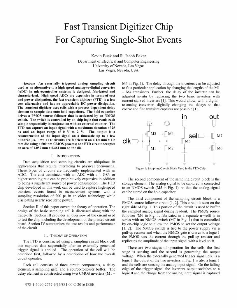
Each cell consists of three circuit components, a delay element, a sampling gate, and a source-follower buffer. The delay element is constructed using two CMOS inverters (M1 –
M4 in Fig. 1). The delay through the inverters can be adjusted to fit a particular application by changing the lengths of the M1 – M4 transistors. Further, the delay of the inverter can be adjusted in-situ by replacing the two basic inverters with current-starved inverters [1]. This would allow, with a digital-to-analog converter, digitally changing the delays so that coarse and fine transient captures are possible [1].
Figure 1: Sampling Circuit Block Used in the FTD Chip.
The second component of the sampling circuit block is the
storage element. The analog signal to be captured is connected to an NMOS switch (M5 in Fig. 1), so that the analog signal can be stored on the hold capacitor.
The third component of the sampling circuit block is a PMOS source follower circuit [1, 2]. This circuit is seen on the right side of Fig. 1. This portion of the circuit is used to buffer the sampled analog signal during readout. The PMOS source follower (M6 in Fig. 1, fabricated in a separate n-well) is in series with an NMOS switch (M7 in Fig. 1) that is controlled by on-chip logic to allow the PMOS to set the output voltage [1, 2]. The NMOS switch is tied to the power supply via a pull-up resistor and when the NMOS gate is driven to a logic 1 the PMOS sets the current through the pull-up resistor and replicates the amplitude of the input signal with a level shift.
There are two stages of operation for the cells, the first stage is sensing and the second is generating the output voltage. When the externally generated trigger signal, clk, is a logic 1 the output of the two inverters in Fig. 1 is also a logic 1 and the cells are sensing the analog input signal. On the falling edge of the trigger signal the inverters output switches to a logic 0 and the charge from the analog input signal is captured
M1 M2
M3 M4
M5
M6
M7
978-1-5090-2757-6/16/$31.00 © 2016 IEEE
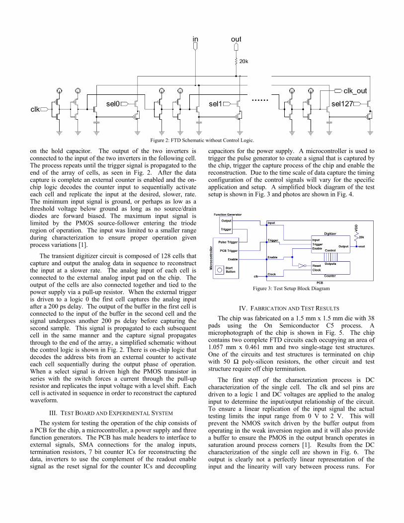
Figure 2: FTD Schematic without Control Logic.
on the hold capacitor. The output of the two inverters is connected to the input of the two inverters in the following cell. The process repeats until the trigger signal is propagated to the end of the array of cells, as seen in Fig. 2. After the data capture is complete an external counter is enabled and the on-chip logic decodes the counter input to sequentially activate each cell and replicate the input at the desired, slower, rate. The minimum input signal is ground, or perhaps as low as a threshold voltage below ground as long as no source/drain diodes are forward biased. The maximum input signal is limited by the PMOS source-follower entering the triode region of operation. The input was limited to a smaller range during characterization to ensure proper operation given process variations [1].
The transient digitizer circuit is composed of 128 cells that capture and output the analog data in sequence to reconstruct the input at a slower rate. The analog input of each cell is connected to the external analog input pad on the chip. The output of the cells are also connected together and tied to the power supply via a pull-up resistor. When the external trigger is driven to a logic 0 the first cell captures the analog input after a 200 ps delay. The output of the buffer in the first cell is connected to the input of the buffer in the second cell and the signal undergoes another 200 ps delay before capturing the second sample. This signal is propagated to each subsequent cell in the same manner and the capture signal propagates through to the end of the array, a simplified schematic without the control logic is shown in Fig. 2. There is on-chip logic that decodes the address bits from an external counter to activate each cell sequentially during the output phase of operation. When a select signal is driven high the PMOS transistor in series with the switch forces a current through the pull-up resistor and replicates the input voltage with a level shift. Each cell is activated in sequence in order to reconstruct the captured waveform.
III. TEST BOARD AND EXPERIMENTAL SYSTEM
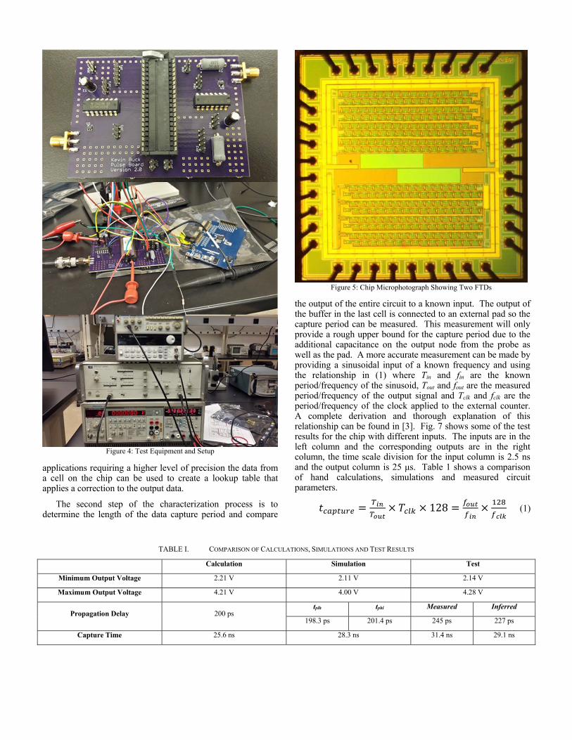
The system for testing the operation of the chip consists of a PCB for the chip, a microcontroller, a power supply and three function generators. The PCB has male headers to interface to external signals, SMA connections for the analog inputs, termination resistors, 7 bit counter ICs for reconstructing the data, inverters to use the complement of the readout enable signal as the reset signal for the counter ICs and decoupling
capacitors for the power supply. A microcontroller is used to trigger the pulse generator to create a signal that is captured by the chip, trigger the capture process of the chip and enable the reconstruction. Due to the time scale of data capture the timing configuration of the control signals will vary for the specific application and setup. A simplified block diagram of the test setup is shown in Fig. 3 and photos are shown in Fig. 4.
Figure 3: Test Setup Block Diagram
IV. FABRICATION AND TEST RESULTS
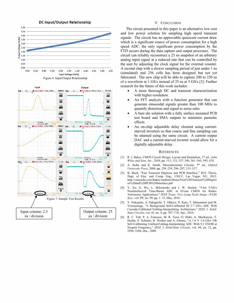
The chip was fabricated on a 1.5 mm x 1.5 mm die with 38 pads using the On Semiconductor C5 process. A microphotograph of the chip is shown in Fig. 5. The chip contains two complete FTD circuits each occupying an area of 1.057 mm x 0.461 mm and two single-stage test structures. One of the circuits and test structures is terminated on chip with 50 Ω poly-silicon resistors, the other circuit and test structure require off chip termination.
The first step of the characterization process is DC characterization of the single cell. The clk and sel pins are driven to a logic 1 and DC voltages are applied to the analog input to determine the input/output relationship of the circuit. To ensure a linear replication of the input signal the actual testing limits the input range from 0 V to 2 V. This will prevent the NMOS switch driven by the buffer output from operating in the weak inversion region and it will also provide a buffer to ensure the PMOS in the output branch operates in saturation around process corners [1]. Results from the DC characterization of the single cell are shown in Fig. 6. The output is clearly not a perfectly linear representation of the input and the linearity will vary between process runs. For
applications requiring a higher level of precision the data from a cell on the chip can be used to create a lookup table that applies a correction to the output data.
The second step of the characterization process is to determine the length of the data capture period and compare
the output of the entire circuit to a known input. The output of the buffer in the last cell is connected to an external pad so the capture period can be measured. This measurement will only provide a rough upper bound for the capture period due to the additional capacitance on the output node from the probe as well as the pad. A more accurate measurement can be made by providing a sinusoidal input of a known frequency and using the relationship in (1) where Tin and fin are the known period/frequency of the sinusoid, Tout and fout are the measured period/frequency of the output signal and Tclk and fclk are the period/frequency of the clock applied to the external counter. A complete derivation and thorough explanation of this relationship can be found in [3]. Fig. 7 shows some of the test results for the chip with different inputs. The inputs are in the left column and the corresponding outputs are in the right column, the time scale division for the input column is 2.5 ns and the output column is 25 μs. Table 1 shows a comparison of hand calculations, simulations and measured circuit parameters.
128 (1)
TABLE I. COMPARISON OF CALCULATIONS, SIMULATIONS AND TEST RESULTS
Calculation Simulation Test
Minimum Output Voltage 2.21 V 2.11 V 2.14 V
Maximum Output Voltage 4.21 V 4.00 V 4.28 V
Propagation Delay 200 ps tplh tphl Measured Inferred
198.3 ps 201.4 ps 245 ps 227 ps
Capture Time 25.6 ns 28.3 ns 31.4 ns 29.1 ns
Figure 4: Test Equipment and Setup
Figure 5: Chip Microphotograph Showing Two FTDs
V. CONCLUSION
The circuit presented in this paper is an alternative low cost and low power solution for sampling high speed transient signals. The circuit has no appreciable quiescent current draw which is a significant source of power consumption for a high speed ADC, the only significant power consumption by the FTD occurs during the data capture and output processes. The circuit can reliably reconstruct a 25 ns snapshot of an arbitrary analog input signal at a reduced rate that can be controlled by the user by adjusting the clock signal for the external counter. A second chip with a slower sampling period of just under 1 ns (simulated) and 256 cells has been designed but not yet fabricated. The new chip will be able to capture 200 to 250 ns of a waveform at 1 GS/s instead of 25 ns at 5 GS/s [3]. Further research for the future of this work includes:
• A more thorough DC and transient characterization with higher resolution.
• An FFT analysis with a function generator that can generate sinusoidal signals greater than 100 MHz to quantify distortion and signal to noise ratio.
• A bare die solution with a fully surface mounted PCB test board and SMA outputs to minimize parasitic effects.
• An on-chip adjustable delay element using current-starved inverters so that coarse and fine sampling can be attained using the same circuit. A current output DAC and a current-starved inverter would allow for a digitally adjustable delay.
REFERENCES [1] R. J. Baker, CMOS Circuit Design, Layout and Simulation, 3rd ed., John
Wiley and Sons, Inc., 2010, pp. 115, 133, 337–340, 561–565, 595, 670.
[2] A. Sedra and K. Smith, Microelectronic Circuits, 5th ed., Oxford University Press, 2004, pp. 258–259, 296–297, 315–317.
[3] K. Buck, “Fast Transient Digitizer and PCB Interface,” M.S. Thesis, Dept. of Elec. and Comp. Eng., UNLV, Las Vegas, NV, 2015. http://cmosedu.com/jbaker/students/theses/Fast%20Transient%20Digitizer%20and%20PCB%20Interface.pdf
[4] Y. Xu, G. Wu, L. Belostotski and J. W. Haslett, “5-bit 5-GS/s Noninterleaved Time-Based ADC in 65-nm CMOS for Radio-Astronomy Applications,” IEEE Trans. Very Large Scale Integr. (VLSI) Syst., vol. PP, no. 99, pp. 1–13, May, 2016.
[5] Y. Nakajima, A. Sakaguchi, T. Ohkico, N. Kato, T. Matsumoto and M. Yotsuyanagi, “A Background Self-Calibrated 6b 2.7 GS/s ADC With Cascade-Calibrated Folding-Interpolating Architecture,” IEEE J. Solid-State Circuits, vol. 45, no. 4, pp. 707–718, Apr., 2010.
[6] R. C. Taft, P. A. Francese, M. R. Tursi, O. Hidri, A. MacKenzie, T. Hoehn, P. Schmitz, H. Werker and A. Glenny, “A 1.8 V 1.0 GS/s 10b Self-Calibrating Unified-Folding-Interpolating ADC With 9.1 ENOB at Nyquist Frequency,” IEEE J. Solid-State Circuits, vol. 44, no. 12, pp. 3294–3304, Dec., 2009.
Figure 6: Input/Output Relationship
Figure 7: Sample Test Results
Input column: 2.5 ns / division
Output column: 25 μs / division