fan7930b — critical conduction mode pfc controller
TRANSCRIPT

November 2013
© 2010 Fairchild Semiconductor Corporation www.fairchildsemi.com FAN7930B • Rev. 1.0.3
FA
N7
93
0B
— C
ritica
l Co
nd
uctio
n M
od
e P
FC
Co
ntro
ller
FAN7930B Critical Conduction Mode PFC Controller
Features
Additional OVP Detection Pin
VIN-Absent Detection
Maximum Switching Frequency Limitation
Internal Soft-Start and Startup without Overshoot
Internal Total Harmonic Distortion (THD) Optimizer
Precise Adjustable Output Over-Voltage Protection
Open-Feedback Protection and Disable Function
Zero Current Detector (ZCD)
150 μs Internal Startup Timer
MOSFET Over-Current Protection (OCP)
Under-Voltage Lockout with 3.5 V Hysteresis
Low Startup and Operating Current
Totem-Pole Output with High State Clamp
+500/-800 mA Peak Gate Drive Current
8-Pin, Small-Outline Package (SOP)
Applications
Adapter
Ballast
LCD TV, CRT TV
SMPS
Description
The FAN7930B is an active power factor correction (PFC) controller for boost PFC applications that operate in critical conduction mode (CRM). It uses a voltage-mode PWM that compares an internal ramp signal with the error amplifier output to generate a MOSFET turn-off signal. Because the voltage-mode CRM PFC controller does not need rectified AC line voltage information, it saves the power loss of an input voltage sensing network necessary for a current-mode CRM PFC controller.
FAN7930B provides over-voltage protection (OVP), open-feedback protection, over-current protection (OCP), input-voltage-absent detection, and under-voltage lockout protection (UVLO). The additional OVP pin can be used to shut down the boost power stage when output voltage exceeds OVP level due to the resistors that are connected at INV pin are damaged. The FAN7930B can be disabled if the INV pin voltage is lower than 0.45 V and the operating current decreases to a very low level. Using a new variable on-time control method, total harmonic distortion (THD) is lower than in conventional CRM boost PFC ICs.
Related Resources
AN-8035 — Design Consideration for Boundary Conduction Mode PFC Using FAN7930
Ordering Information
Part Number Operating
Temperature Range Top Mark Package
Packing Method
FAN7930BMX_G -40 to +125°C FAN7930BG 8-Lead, Small-Outline Package (SOP) Tape & Reel
© 2010 Fairchild Semiconductor Corporation www.fairchildsemi.com FAN7930B • Rev. 1.0.3 2
FA
N7
93
0B
— C
ritica
l Co
nd
uctio
n M
od
e P
FC
Co
ntro
ller
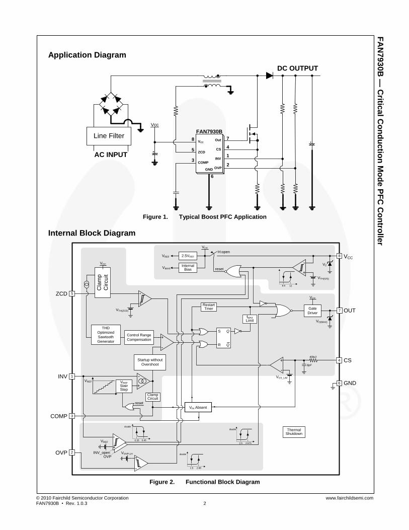
Application Diagram
AC INPUT
DC OUTPUT
Line Filter
1
7
6
8
5
3
4
2
FAN7930B
COMPINV
VCCOut
GND
ZCDCS
OVP
Vcc
Figure 1. Typical Boost PFC Application
Internal Block Diagram
VCC
ZCD
VTH(ZCD)
VCC
OUT
+
-
S
QR
Q
+
-INV 1
5
COMP 3
Clamp Circuit
+
-VCS_LIM
40kW
8pF
4 CS
0.450.35
disable
2.6752.5
disable
+
-
VZ
+
-
VTH(S/S)
128.5
VO(MAX)
VCC
2.5VREF
Internal Bias
VBIAS
VREF
Gate
Driver
Restart Tmer
7
8
6 GND
+
-
INV_openOVP
OVP 2
reset
reset
H:open
Thermal Shutdown
fMAX Limit
VREF
Startup without
Overshoot
VREF Stair Step
Cla
mp
Circu
it
THD
Optimized
Sawtooth
Generator
VIN Absent
VCC
2.882.5
disable
+
-
VOVP,LH
VREF
Control Range
Compensation
Figure 2. Functional Block Diagram
© 2010 Fairchild Semiconductor Corporation www.fairchildsemi.com FAN7930B • Rev. 1.0.3 3
FA
N7
93
0B
— C
ritica
l Co
nd
uctio
n M
od
e P
FC
Co
ntro
ller
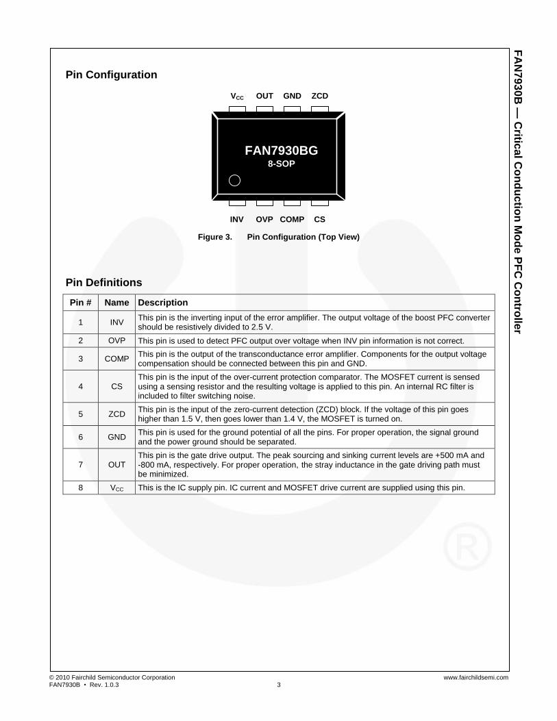
Pin Configuration
INV OVP CS
ZCD
FAN7930BG8-SOP
COMP
VCC OUT GND
Figure 3. Pin Configuration (Top View)
Pin Definitions
Pin # Name Description
1 INV This pin is the inverting input of the error amplifier. The output voltage of the boost PFC converter should be resistively divided to 2.5 V.
2 OVP This pin is used to detect PFC output over voltage when INV pin information is not correct.
3 COMP This pin is the output of the transconductance error amplifier. Components for the output voltage compensation should be connected between this pin and GND.
4 CS This pin is the input of the over-current protection comparator. The MOSFET current is sensed using a sensing resistor and the resulting voltage is applied to this pin. An internal RC filter is included to filter switching noise.
5 ZCD This pin is the input of the zero-current detection (ZCD) block. If the voltage of this pin goes higher than 1.5 V, then goes lower than 1.4 V, the MOSFET is turned on.
6 GND This pin is used for the ground potential of all the pins. For proper operation, the signal ground and the power ground should be separated.
7 OUT This pin is the gate drive output. The peak sourcing and sinking current levels are +500 mA and -800 mA, respectively. For proper operation, the stray inductance in the gate driving path must be minimized.
8 VCC This is the IC supply pin. IC current and MOSFET drive current are supplied using this pin.
© 2010 Fairchild Semiconductor Corporation www.fairchildsemi.com FAN7930B • Rev. 1.0.3 4
FA
N7
93
0B
— C
ritica
l Co
nd
uctio
n M
od
e P
FC
Co
ntro
ller
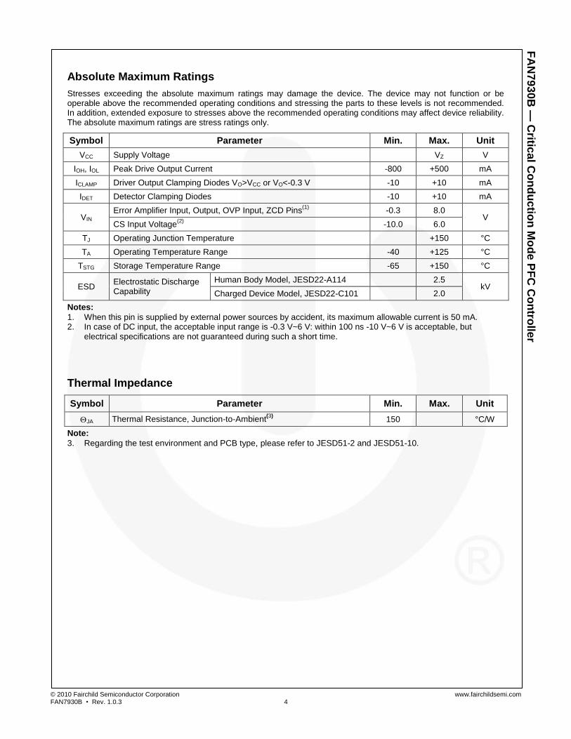
Absolute Maximum Ratings
Stresses exceeding the absolute maximum ratings may damage the device. The device may not function or be operable above the recommended operating conditions and stressing the parts to these levels is not recommended. In addition, extended exposure to stresses above the recommended operating conditions may affect device reliability. The absolute maximum ratings are stress ratings only.
Symbol Parameter Min. Max. Unit
VCC Supply Voltage VZ V
IOH, IOL Peak Drive Output Current -800 +500 mA
ICLAMP Driver Output Clamping Diodes VO>VCC or VO<-0.3 V -10 +10 mA
IDET Detector Clamping Diodes -10 +10 mA
VIN Error Amplifier Input, Output, OVP Input, ZCD Pins
(1) -0.3 8.0
V CS Input Voltage
(2) -10.0 6.0
TJ Operating Junction Temperature +150 °C
TA Operating Temperature Range -40 +125 °C
TSTG Storage Temperature Range -65 +150 °C
ESD Electrostatic Discharge Capability
Human Body Model, JESD22-A114 2.5 kV
Charged Device Model, JESD22-C101 2.0
Notes:
1. When this pin is supplied by external power sources by accident, its maximum allowable current is 50 mA. 2. In case of DC input, the acceptable input range is -0.3 V~6 V: within 100 ns -10 V~6 V is acceptable, but
electrical specifications are not guaranteed during such a short time.
Thermal Impedance
Symbol Parameter Min. Max. Unit
JA Thermal Resistance, Junction-to-Ambient(3)
150 °C/W
Note:
3. Regarding the test environment and PCB type, please refer to JESD51-2 and JESD51-10.
© 2010 Fairchild Semiconductor Corporation www.fairchildsemi.com FAN7930B • Rev. 1.0.3 5
FA
N7
93
0B
— C
ritica
l Co
nd
uctio
n M
od
e P
FC
Co
ntro
ller
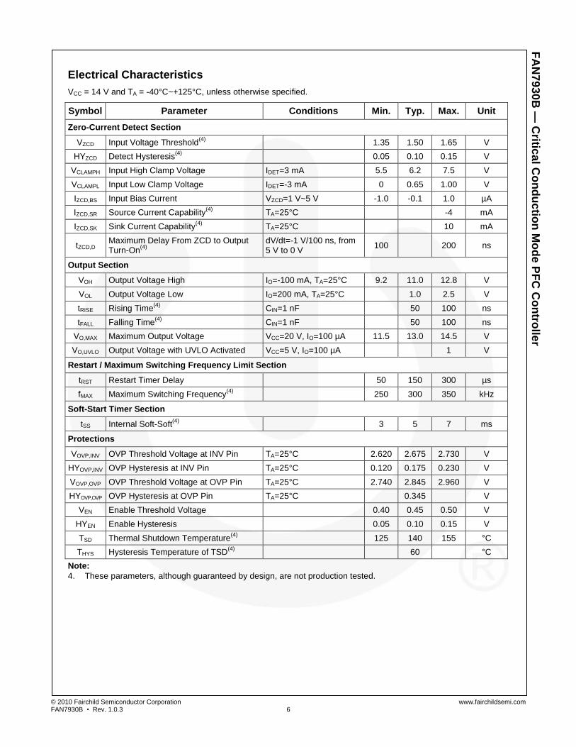
Electrical Characteristics
VCC = 14 V and TA = -40°C~+125°C, unless otherwise specified.
Symbol Parameter Conditions Min. Typ. Max. Unit
VCC Section
VSTART Start Threshold Voltage VCC Increasing 11 12 13 V
VSTOP Stop Threshold Voltage VCC Decreasing 7.5 8.5 9.5 V
HYUVLO UVLO Hysteresis 3.0 3.5 4.0 V
VZ Zener Voltage ICC=20 mA 20 22 24 V
VOP Recommended Operating Range 13 20 V
Supply Current Section
ISTART Startup Supply Current VCC=VSTART-0.2 V 120 190 µA
IOP Operating Supply Current Output Not Switching 1.5 3.0 mA
IDOP Dynamic Operating Supply Current 50 kHz, CI=1 nF 2.5 4.0 mA
IOPDIS Operating Current at Disable VINV=0 V 90 160 230 µA
Error Amplifier Section
VREF1 Voltage Feedback Input Threshold1 TA=25°C 2.465 2.500 2.535 V
VREF1 Line Regulation VCC=14 V~20 V 0.1 10.0 mV
VREF2 Temperature Stability of VREF1(4)
20 mV
IEA,BS Input Bias Current VINV=1 V~4 V -0.5 0.5 µA
IEAS,SR Output Source Current VINV=VREF -0.1 V -12 µA
IEAS,SK Output Sink Current VINV=VREF +0.1 V 12 µA
VEAH Output Upper Clamp Voltage VINV=1 V, VCS=0 V 6.0 6.5 7.0 V
VEAZ Zero Duty Cycle Output Voltage 0.9 1.0 1.1 V
gm Transconductance(4)
90 115 140 µmho
Maximum On-Time Section
tON,MAX1 Maximum On-Time Programming 1 TA=25°C, VZCD=1 V 35.5 41.5 47.5 µs
tON,MAX2 Maximum On-Time Programming 2 TA=25°C, IZCD=0.469 mA
11.2 13.0 14.8 µs
Current-Sense Section
VCS Current Sense Input Threshold Voltage Limit
0.7 0.8 0.9 V
ICS,BS Input Bias Current VCS=0~1 V -1.0 -0.1 1.0 µA
tCS,D Current Sense Delay to Output(4)
dV/dt=1 V/100 ns, from 0 V to 5 V
350 500 ns
Continued on the following page…
© 2010 Fairchild Semiconductor Corporation www.fairchildsemi.com FAN7930B • Rev. 1.0.3 6
FA
N7
93
0B
— C
ritica
l Co
nd
uctio
n M
od
e P
FC
Co
ntro
ller
Electrical Characteristics
VCC = 14 V and TA = -40°C~+125°C, unless otherwise specified.
Symbol Parameter Conditions Min. Typ. Max. Unit
Zero-Current Detect Section
VZCD Input Voltage Threshold(4)
1.35 1.50 1.65 V
HYZCD Detect Hysteresis(4)
0.05 0.10 0.15 V
VCLAMPH Input High Clamp Voltage IDET=3 mA 5.5 6.2 7.5 V
VCLAMPL Input Low Clamp Voltage IDET=-3 mA 0 0.65 1.00 V
IZCD,BS Input Bias Current VZCD=1 V~5 V -1.0 -0.1 1.0 µA
IZCD,SR Source Current Capability(4)
TA=25°C -4 mA
IZCD,SK Sink Current Capability(4)
TA=25°C 10 mA
tZCD,D Maximum Delay From ZCD to Output Turn-On
(4)
dV/dt=-1 V/100 ns, from 5 V to 0 V
100 200 ns
Output Section
VOH Output Voltage High IO=-100 mA, TA=25°C 9.2 11.0 12.8 V
VOL Output Voltage Low IO=200 mA, TA=25°C 1.0 2.5 V
tRISE Rising Time(4)
CIN=1 nF 50 100 ns
tFALL Falling Time(4)
CIN=1 nF 50 100 ns
VO,MAX Maximum Output Voltage VCC=20 V, IO=100 µA 11.5 13.0 14.5 V
VO,UVLO Output Voltage with UVLO Activated VCC=5 V, IO=100 µA 1 V
Restart / Maximum Switching Frequency Limit Section
tRST Restart Timer Delay 50 150 300 µs
fMAX Maximum Switching Frequency(4)
250 300 350 kHz
Soft-Start Timer Section
tSS Internal Soft-Soft(4)
3 5 7 ms
Protections
VOVP,INV OVP Threshold Voltage at INV Pin TA=25°C 2.620 2.675 2.730 V
HYOVP,INV OVP Hysteresis at INV Pin TA=25°C 0.120 0.175 0.230 V
VOVP,OVP OVP Threshold Voltage at OVP Pin TA=25°C 2.740 2.845 2.960 V
HYOVP,OVP OVP Hysteresis at OVP Pin TA=25°C 0.345 V
VEN Enable Threshold Voltage 0.40 0.45 0.50 V
HYEN Enable Hysteresis 0.05 0.10 0.15 V
TSD Thermal Shutdown Temperature(4)
125 140 155 °C
THYS Hysteresis Temperature of TSD(4)
60 °C
Note:
4. These parameters, although guaranteed by design, are not production tested.
© 2010 Fairchild Semiconductor Corporation www.fairchildsemi.com FAN7930B • Rev. 1.0.3 7
FA
N7
93
0B
— C
ritica
l Co
nd
uctio
n M
od
e P
FC
Co
ntro
ller
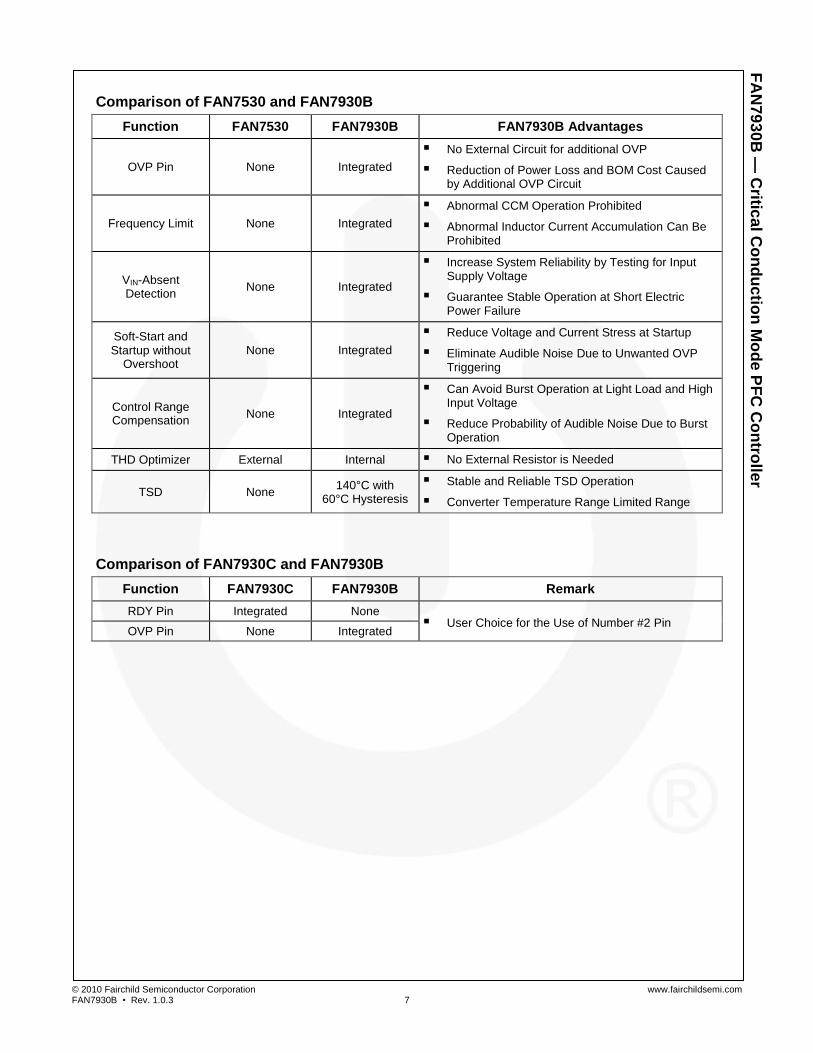
Comparison of FAN7530 and FAN7930B
Function FAN7530 FAN7930B FAN7930B Advantages
OVP Pin None Integrated
No External Circuit for additional OVP
Reduction of Power Loss and BOM Cost Caused by Additional OVP Circuit
Frequency Limit None Integrated
Abnormal CCM Operation Prohibited
Abnormal Inductor Current Accumulation Can Be Prohibited
VIN-Absent Detection
None Integrated
Increase System Reliability by Testing for Input Supply Voltage
Guarantee Stable Operation at Short Electric Power Failure
Soft-Start and Startup without
Overshoot None Integrated
Reduce Voltage and Current Stress at Startup
Eliminate Audible Noise Due to Unwanted OVP Triggering
Control Range Compensation
None Integrated
Can Avoid Burst Operation at Light Load and High Input Voltage
Reduce Probability of Audible Noise Due to Burst Operation
THD Optimizer External Internal No External Resistor is Needed
TSD None 140°C with
60°C Hysteresis
Stable and Reliable TSD Operation
Converter Temperature Range Limited Range
Comparison of FAN7930C and FAN7930B
Function FAN7930C FAN7930B Remark
RDY Pin Integrated None User Choice for the Use of Number #2 Pin
OVP Pin None Integrated
© 2010 Fairchild Semiconductor Corporation www.fairchildsemi.com FAN7930B • Rev. 1.0.3 8
FA
N7
93
0B
— C
ritica
l Co
nd
uctio
n M
od
e P
FC
Co
ntro
ller
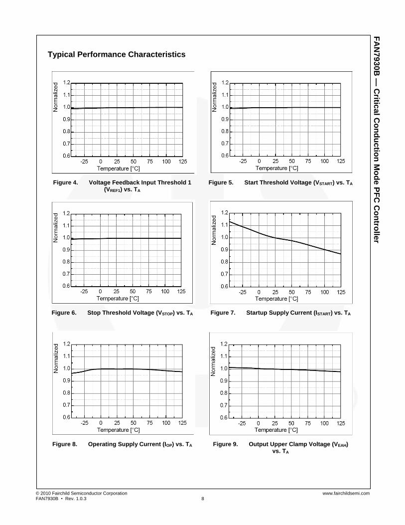
Typical Performance Characteristics
Figure 4. Voltage Feedback Input Threshold 1 (VREF1) vs. TA
Figure 5. Start Threshold Voltage (VSTART) vs. TA
Figure 6. Stop Threshold Voltage (VSTOP) vs. TA Figure 7. Startup Supply Current (ISTART) vs. TA
Figure 8. Operating Supply Current (IOP) vs. TA Figure 9. Output Upper Clamp Voltage (VEAH) vs. TA
© 2010 Fairchild Semiconductor Corporation www.fairchildsemi.com FAN7930B • Rev. 1.0.3 9
FA
N7
93
0B
— C
ritica
l Co
nd
uctio
n M
od
e P
FC
Co
ntro
ller
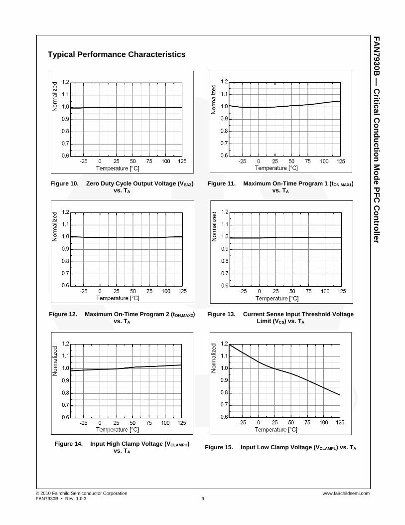
Typical Performance Characteristics
Figure 10. Zero Duty Cycle Output Voltage (VEAZ) vs. TA
Figure 11. Maximum On-Time Program 1 (tON,MAX1) vs. TA
Figure 12. Maximum On-Time Program 2 (tON,MAX2) vs. TA
Figure 13. Current Sense Input Threshold Voltage Limit (VCS) vs. TA
Figure 14. Input High Clamp Voltage (VCLAMPH)
vs. TA Figure 15. Input Low Clamp Voltage (VCLAMPL) vs. TA
© 2010 Fairchild Semiconductor Corporation www.fairchildsemi.com FAN7930B • Rev. 1.0.3 10
FA
N7
93
0B
— C
ritica
l Co
nd
uctio
n M
od
e P
FC
Co
ntro
ller
Typical Performance Characteristics
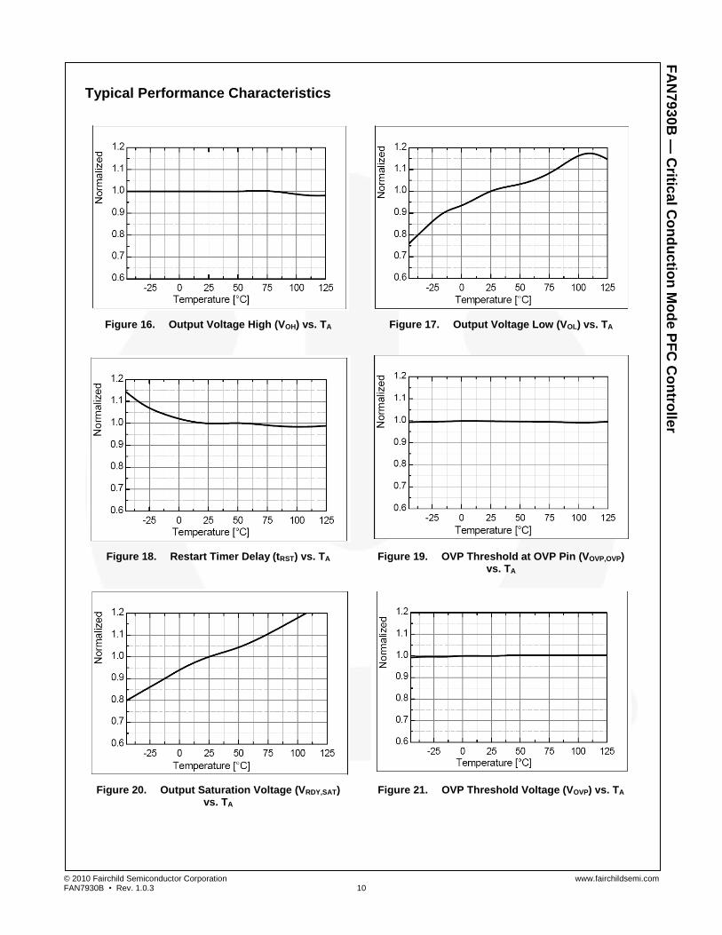
Figure 16. Output Voltage High (VOH) vs. TA Figure 17. Output Voltage Low (VOL) vs. TA
Figure 18. Restart Timer Delay (tRST) vs. TA Figure 19. OVP Threshold at OVP Pin (VOVP,OVP) vs. TA
Figure 20. Output Saturation Voltage (VRDY,SAT) vs. TA
Figure 21. OVP Threshold Voltage (VOVP) vs. TA
© 2010 Fairchild Semiconductor Corporation www.fairchildsemi.com FAN7930B • Rev. 1.0.3 11
FA
N7
93
0B
— C
ritica
l Co
nd
uctio
n M
od
e P
FC
Co
ntro
ller
Applications Information
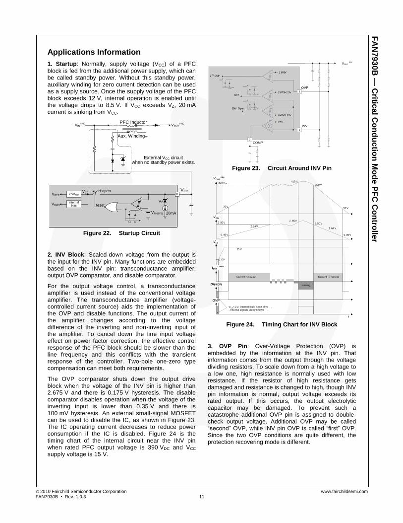
1. Startup: Normally, supply voltage (VCC) of a PFC
block is fed from the additional power supply, which can be called standby power. Without this standby power, auxiliary winding for zero current detection can be used as a supply source. Once the supply voltage of the PFC block exceeds 12 V, internal operation is enabled until the voltage drops to 8.5 V. If VCC exceeds VZ, 20 mA current is sinking from VCC.
VCC
VZ
+
-
VTH(S/S)
128.5
VCC’2.5VREF
internal biasVBIAS
VREF
reset
H:open
20mA
PFC Inductor
Aux. Winding
VINPFC
VOUTPFC
External VCC circuit when no standby power exists.
8
Figure 22. Startup Circuit
2. INV Block: Scaled-down voltage from the output is
the input for the INV pin. Many functions are embedded based on the INV pin: transconductance amplifier, output OVP comparator, and disable comparator.
For the output voltage control, a transconductance amplifier is used instead of the conventional voltage amplifier. The transconductance amplifier (voltage-controlled current source) aids the implementation of the OVP and disable functions. The output current of the amplifier changes according to the voltage difference of the inverting and non-inverting input of the amplifier. To cancel down the line input voltage effect on power factor correction, the effective control response of the PFC block should be slower than the line frequency and this conflicts with the transient response of the controller. Two-pole one-zero type compensation can meet both requirements.
The OVP comparator shuts down the output drive block when the voltage of the INV pin is higher than 2.675 V and there is 0.175 V hysteresis. The disable comparator disables operation when the voltage of the inverting input is lower than 0.35 V and there is 100 mV hysteresis. An external small-signal MOSFET can be used to disable the IC, as shown in Figure 23. The IC operating current decreases to reduce power consumption if the IC is disabled. Figure 24 is the timing chart of the internal circuit near the INV pin when rated PFC output voltage is 390 VDC and VCC
supply voltage is 15 V.
Figure 23. Circuit Around INV Pin
Figure 24. Timing Chart for INV Block
3. OVP Pin: Over-Voltage Protection (OVP) is
embedded by the information at the INV pin. That information comes from the output through the voltage dividing resistors. To scale down from a high voltage to a low one, high resistance is normally used with low resistance. If the resistor of high resistance gets damaged and resistance is changed to high, though INV pin information is normal, output voltage exceeds its rated output. If this occurs, the output electrolytic capacitor may be damaged. To prevent such a catastrophe additional OVP pin is assigned to double-check output voltage. Additional OVP may be called “second” OVP, while INV pin OVP is called “first” OVP. Since the two OVP conditions are quite different, the protection recovering mode is different.
390 V DC
2 . 50 V 2 . 65 V
0 . 45 V
Current Sourcing Current S ourcing I sinking
0 . 35 V 1 . 64 V 2 . 24 V 2 . 50 V
2 . 0 V
413 V 390 V
70 V 55 V
V OUT PFC
V INV
V CC
I OUT COMP
Disable
OVP
t
V CC < 2 V , internal logic is not alive . - Internal signals are unknown .
15 V
+ -
+ -
+ -
V OUT PFC
+ -
2 . 5 V 0 . 45 V / 0 . 35 V
INV O pen
2 . 675 V / 2 . 5 V OVP
2 . 885 V
1 INV
3 COMP
0 . 45 0 . 35 disable
2 . 675 2 . 5 disable
OVP 2
2 nd OVP
2 . 885 high
© 2010 Fairchild Semiconductor Corporation www.fairchildsemi.com FAN7930B • Rev. 1.0.3 12
FA
N7
93
0B
— C
ritica
l Co
nd
uctio
n M
od
e P
FC
Co
ntro
ller
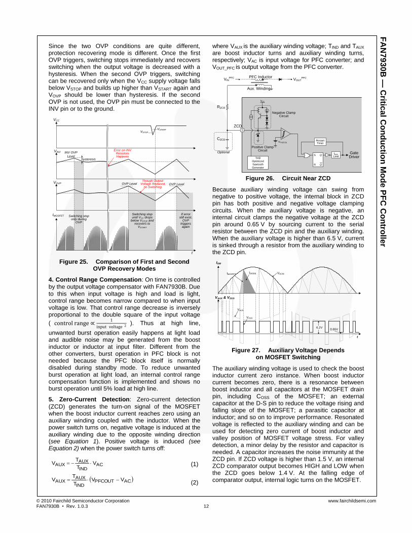
Since the two OVP conditions are quite different, protection recovering mode is different. Once the first OVP triggers, switching stops immediately and recovers switching when the output voltage is decreased with a hysteresis. When the second OVP triggers, switching can be recovered only when the VCC supply voltage falls below VSTOP and builds up higher than VSTART again and VOVP should be lower than hysteresis. If the second OVP is not used, the OVP pin must be connected to the INV pin or to the ground.
VCC
VINV
VOVP
IMOSFET
t
INV OVP
Levelhysteresis
Switching stop only during
OVP
Error on INV Resistors Happens
OVP Level
VSTOP
VSTART
Switching stop until VCC drops
below VSTOP and recovers to
VSTART
If error still exist,
OVP triggers again
OVP LevelThough Output-
Voltage Reduced, no Switching.
Figure 25. Comparison of First and Second
OVP Recovery Modes
4. Control Range Compensation: On time is controlled
by the output voltage compensator with FAN7930B. Due to this when input voltage is high and load is light, control range becomes narrow compared to when input voltage is low. That control range decrease is inversely proportional to the double square of the input voltage
( control range ∝1
input voltage 2 ). Thus at high line,
unwanted burst operation easily happens at light load and audible noise may be generated from the boost inductor or inductor at input filter. Different from the other converters, burst operation in PFC block is not needed because the PFC block itself is normally disabled during standby mode. To reduce unwanted burst operation at light load, an internal control range compensation function is implemented and shows no burst operation until 5% load at high line.
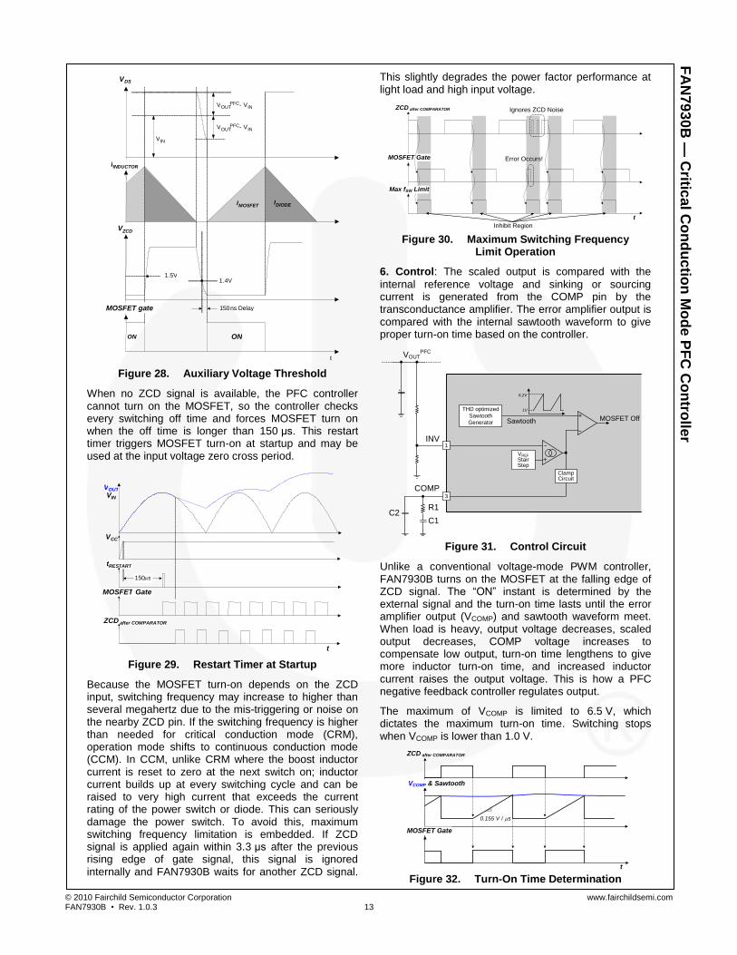
5. Zero-Current Detection: Zero-current detection
(ZCD) generates the turn-on signal of the MOSFET when the boost inductor current reaches zero using an auxiliary winding coupled with the inductor. When the power switch turns on, negative voltage is induced at the auxiliary winding due to the opposite winding direction (see Equation 1). Positive voltage is induced (see Equation 2) when the power switch turns off:
ACIND
AUXAUX V
T
TV
(1)
ACPFCOUTIND
AUXAUX VV
T
TV
(2)
where VAUX is the auxiliary winding voltage; TIND and TAUX are boost inductor turns and auxiliary winding turns, respectively; VAC is input voltage for PFC converter; and VOUT_PFC is output voltage from the PFC converter.
PFC Inductor
Aux. Winding
VINPFC
VOUTPFC
ZCD
VTH(ZCD)
+
-
VCC
THD
Optimized
Sawtooth
Generator
Restart Timer
GateDriver
RZCD
CZCD
Negative Clamp Circuit
Positive Clamp Circuit
5
S
QR
QfMAX
Limit
Optional
Figure 26. Circuit Near ZCD
Because auxiliary winding voltage can swing from negative to positive voltage, the internal block in ZCD pin has both positive and negative voltage clamping circuits. When the auxiliary voltage is negative, an internal circuit clamps the negative voltage at the ZCD pin around 0.65 V by sourcing current to the serial resistor between the ZCD pin and the auxiliary winding. When the auxiliary voltage is higher than 6.5 V, current is sinked through a resistor from the auxiliary winding to the ZCD pin.
ISW
VAUX & VZCD
VACINIMOSFETIDIODE
VAUX
VZCD
t
6.2V0.65V
Figure 27. Auxiliary Voltage Depends
on MOSFET Switching
The auxiliary winding voltage is used to check the boost inductor current zero instance. When boost inductor current becomes zero, there is a resonance between boost inductor and all capacitors at the MOSFET drain pin, including COSS of the MOSFET; an external capacitor at the D-S pin to reduce the voltage rising and falling slope of the MOSFET; a parasitic capacitor at inductor; and so on to improve performance. Resonated voltage is reflected to the auxiliary winding and can be used for detecting zero current of boost inductor and valley position of MOSFET voltage stress. For valley detection, a minor delay by the resistor and capacitor is needed. A capacitor increases the noise immunity at the ZCD pin. If ZCD voltage is higher than 1.5 V, an internal ZCD comparator output becomes HIGH and LOW when the ZCD goes below 1.4 V. At the falling edge of comparator output, internal logic turns on the MOSFET.
© 2010 Fairchild Semiconductor Corporation www.fairchildsemi.com FAN7930B • Rev. 1.0.3 13
FA
N7
93
0B
— C
ritica
l Co
nd
uctio
n M
od
e P
FC
Co
ntro
ller
Figure 28. Auxiliary Voltage Threshold
When no ZCD signal is available, the PFC controller cannot turn on the MOSFET, so the controller checks every switching off time and forces MOSFET turn on when the off time is longer than 150 μs. This restart timer triggers MOSFET turn-on at startup and may be used at the input voltage zero cross period.
Figure 29. Restart Timer at Startup
Because the MOSFET turn-on depends on the ZCD input, switching frequency may increase to higher than several megahertz due to the mis-triggering or noise on the nearby ZCD pin. If the switching frequency is higher than needed for critical conduction mode (CRM), operation mode shifts to continuous conduction mode (CCM). In CCM, unlike CRM where the boost inductor current is reset to zero at the next switch on; inductor current builds up at every switching cycle and can be raised to very high current that exceeds the current rating of the power switch or diode. This can seriously damage the power switch. To avoid this, maximum switching frequency limitation is embedded. If ZCD signal is applied again within 3.3 μs after the previous rising edge of gate signal, this signal is ignored internally and FAN7930B waits for another ZCD signal.
This slightly degrades the power factor performance at light load and high input voltage.
ZCD after COMPARATOR
MOSFET Gate
Max fSW Limit
Inhibit Region
Error Occurs!
Ignores ZCD Noise
t
Figure 30. Maximum Switching Frequency
Limit Operation
6. Control: The scaled output is compared with the
internal reference voltage and sinking or sourcing current is generated from the COMP pin by the transconductance amplifier. The error amplifier output is compared with the internal sawtooth waveform to give proper turn-on time based on the controller.
VOUTPFC
+
-INV
1
COMP3
Clamp Circuit
+
-
VREF Stair Step
THD optimized
Sawtooth
Generator Sawtooth MOSFET Off
R1
C1C2
1V
6.2V
Figure 31. Control Circuit
Unlike a conventional voltage-mode PWM controller, FAN7930B turns on the MOSFET at the falling edge of ZCD signal. The “ON” instant is determined by the external signal and the turn-on time lasts until the error amplifier output (VCOMP) and sawtooth waveform meet. When load is heavy, output voltage decreases, scaled output decreases, COMP voltage increases to compensate low output, turn-on time lengthens to give more inductor turn-on time, and increased inductor current raises the output voltage. This is how a PFC negative feedback controller regulates output.
The maximum of VCOMP is limited to 6.5 V, which dictates the maximum turn-on time. Switching stops when VCOMP is lower than 1.0 V.
ZCD after COMPARATOR
VCOMP & Sawtooth
MOSFET Gate
t
s/V155.0
Figure 32. Turn-On Time Determination
V OUT V IN
V CC
t RESTART
MOSFET G ate
ZCD after COMPARATOR
t
s 150
V IN
V OUT PFC - V IN
1 . 5 V
150 ns Delay
1 . 4 V
ON ON
V OUT PFC - V IN
I MOSFET I DIODE
V ZCD
t
I INDUCTOR
V DS
MOSFET gate
© 2010 Fairchild Semiconductor Corporation www.fairchildsemi.com FAN7930B • Rev. 1.0.3 14
FA
N7
93
0B
— C
ritica
l Co
nd
uctio
n M
od
e P
FC
Co
ntro
ller
The roles of PFC controller are regulating output voltage and input current shaping to increase power factor. Duty control based on the output voltage should be fast enough to compensate output voltage dip or overshoot. For the power factor, however, the control loop must not react to the fluctuating AC input voltage. These two requirements conflict; therefore, when designing a feedback loop, the feedback loop should be least ten times slower than AC line frequency. That slow response is made by C1 at the compensator. R1 makes gain boost around operation region and C2 attenuates gain at higher frequency. Boost gain by R1 helps raise the response time and improves phase margin.
Freq.
C1
R1
Proportional
Gain
C2
Integrator
High-Frequency
Noise Filter
Gain
Figure 33. Compensators Gain Curve
For the transconductance error amplifier side, gain changes based on differential input. When the error is large, gain is large to suppress the output dip or peak quickly. When the error is small, low gain is used to improve power factor performance.
ICOMP
So
urc
ing
Sin
kin
g
Powering
Braking
2.5
V
2.4
V
2.6
V
mho250
mho115
Figure 34. Gain Characteristic
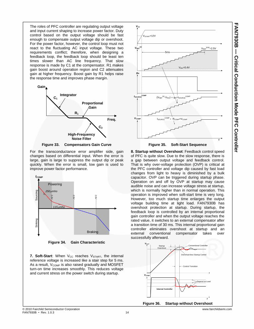
7. Soft-Start: When VCC reaches VSTART, the internal
reference voltage is increased like a stair step for 5 ms. As a result, VCOMP is also raised gradually and MOSFET turn-on time increases smoothly. This reduces voltage and current stress on the power switch during startup.
VREFSS
gM
VINV=0.4V
ISOURCECOMP
VCOMP ISOURCECOMP
RCOMP=VCOMP
t
(VREFSS
-VINV)
gM=ISOURCECOMP
VREFEND
=2.5V
5ms
VCC
VSTART=12V
Figure 35. Soft-Start Sequence
8. Startup without Overshoot: Feedback control speed
of PFC is quite slow. Due to the slow response, there is a gap between output voltage and feedback control. That is why over-voltage protection (OVP) is critical at the PFC controller and voltage dip caused by fast load changes from light to heavy is diminished by a bulk capacitor. OVP can be triggered during startup phase. Operation on and off by OVP at startup may cause audible noise and can increase voltage stress at startup, which is normally higher than in normal operation. This operation is improved when soft-start time is very long. However, too much startup time enlarges the output voltage building time at light load. FAN7930B has overshoot protection at startup. During startup, the feedback loop is controlled by an internal proportional gain controller and when the output voltage reaches the rated value, it switches to an external compensator after a transition time of 30 ms. This internal proportional gain controller eliminates overshoot at startup and an external conventional compensator takes over successfully afterward.
Depend on Load
VOUT
VCOMP
Startup
Overshoot
Internal Controller
t
Conventional Controller
Overshoot-less Startup Control
Control Transition
Figure 36. Startup without Overshoot
© 2010 Fairchild Semiconductor Corporation www.fairchildsemi.com FAN7930B • Rev. 1.0.3 15
FA
N7
93
0B
— C
ritica
l Co
nd
uctio
n M
od
e P
FC
Co
ntro
ller
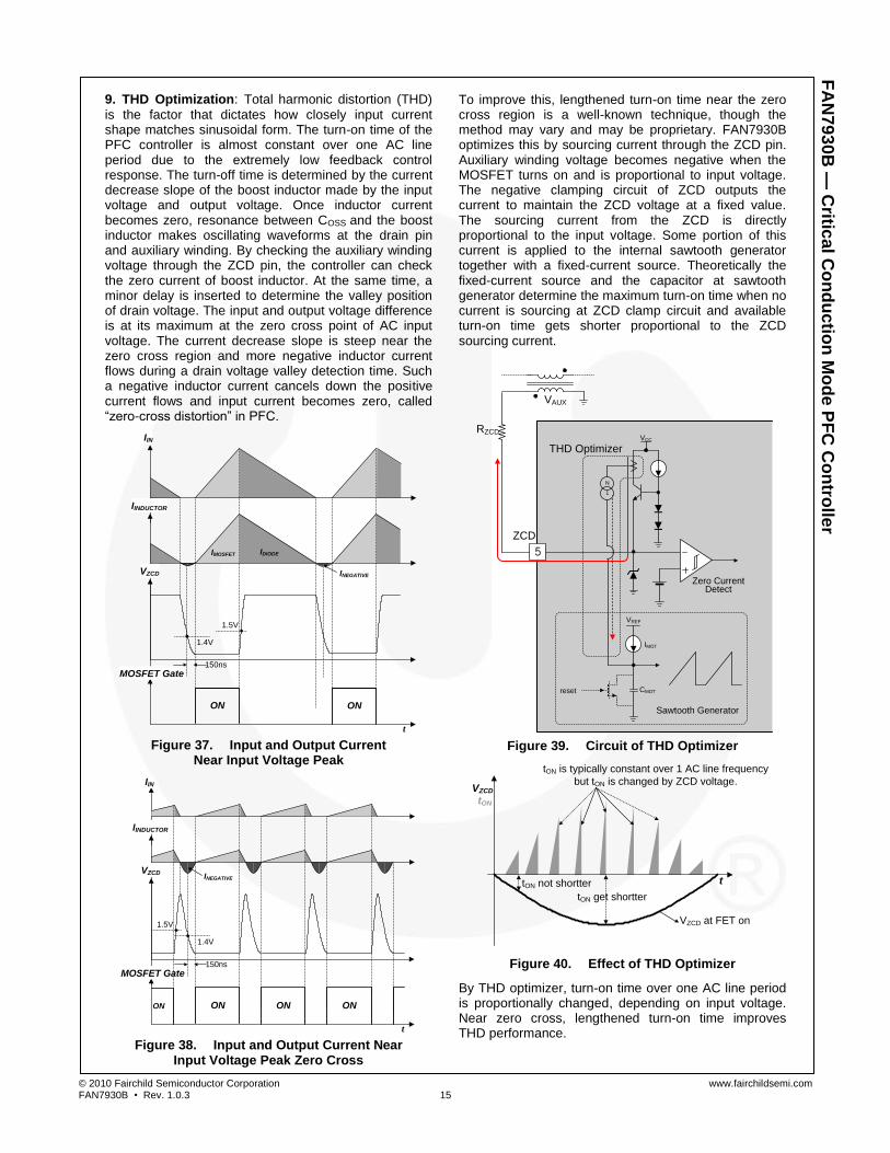
9. THD Optimization: Total harmonic distortion (THD)
is the factor that dictates how closely input current shape matches sinusoidal form. The turn-on time of the PFC controller is almost constant over one AC line period due to the extremely low feedback control response. The turn-off time is determined by the current decrease slope of the boost inductor made by the input voltage and output voltage. Once inductor current becomes zero, resonance between COSS and the boost inductor makes oscillating waveforms at the drain pin and auxiliary winding. By checking the auxiliary winding voltage through the ZCD pin, the controller can check the zero current of boost inductor. At the same time, a minor delay is inserted to determine the valley position of drain voltage. The input and output voltage difference is at its maximum at the zero cross point of AC input voltage. The current decrease slope is steep near the zero cross region and more negative inductor current flows during a drain voltage valley detection time. Such a negative inductor current cancels down the positive current flows and input current becomes zero, called “zero-cross distortion” in PFC.
1.5V
150ns
1.4V
ON
VZCD
t
IINDUCTOR
MOSFET Gate
INEGATIVE
ON
IIN
IMOSFET IDIODE
Figure 37. Input and Output Current
Near Input Voltage Peak
1.5V
150ns
1.4V
ONON
VZCD
t
IINDUCTOR
MOSFET Gate
INEGATIVE
ON ON
IIN
Figure 38. Input and Output Current Near
Input Voltage Peak Zero Cross
To improve this, lengthened turn-on time near the zero cross region is a well-known technique, though the method may vary and may be proprietary. FAN7930B optimizes this by sourcing current through the ZCD pin. Auxiliary winding voltage becomes negative when the MOSFET turns on and is proportional to input voltage. The negative clamping circuit of ZCD outputs the current to maintain the ZCD voltage at a fixed value. The sourcing current from the ZCD is directly proportional to the input voltage. Some portion of this current is applied to the internal sawtooth generator together with a fixed-current source. Theoretically the fixed-current source and the capacitor at sawtooth generator determine the maximum turn-on time when no current is sourcing at ZCD clamp circuit and available turn-on time gets shorter proportional to the ZCD sourcing current.
RZCD
VAUX
ZCD
Zero Current Detect
5
VCC
N
1
VREF
IMOT
reset
Sawtooth Generator
CMOT
THD Optimizer
Figure 39. Circuit of THD Optimizer
VZCD
tON
t
VZCD at FET on
tON get shortter
tON not shortter
tON is typically constant over 1 AC line frequency
but tON is changed by ZCD voltage.
Figure 40. Effect of THD Optimizer
By THD optimizer, turn-on time over one AC line period is proportionally changed, depending on input voltage. Near zero cross, lengthened turn-on time improves THD performance.
© 2010 Fairchild Semiconductor Corporation www.fairchildsemi.com FAN7930B • Rev. 1.0.3 16
FA
N7
93
0B
— C
ritica
l Co
nd
uctio
n M
od
e P
FC
Co
ntro
ller
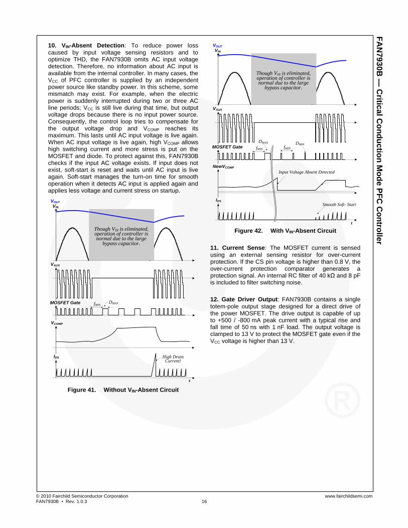
10. VIN-Absent Detection: To reduce power loss
caused by input voltage sensing resistors and to optimize THD, the FAN7930B omits AC input voltage detection. Therefore, no information about AC input is available from the internal controller. In many cases, the VCC of PFC controller is supplied by an independent power source like standby power. In this scheme, some mismatch may exist. For example, when the electric power is suddenly interrupted during two or three AC line periods; VCC is still live during that time, but output voltage drops because there is no input power source. Consequently, the control loop tries to compensate for the output voltage drop and VCOMP reaches its maximum. This lasts until AC input voltage is live again. When AC input voltage is live again, high VCOMP allows high switching current and more stress is put on the MOSFET and diode. To protect against this, FAN7930B checks if the input AC voltage exists. If input does not exist, soft-start is reset and waits until AC input is live again. Soft-start manages the turn-on time for smooth operation when it detects AC input is applied again and applies less voltage and current stress on startup.
VIN
t
VOUT
VAUX
MOSFET Gate
IDS
fMINDMAX
High Drain Current!
VCOMP
Though VIN is eliminated, operation of controller is normal due to the large
bypass capacitor.
Figure 41. Without VIN-Absent Circuit
VIN
t
VOUT
VAUX
MOSFET Gate
IDS
fMIN
DMAX
Input Voltage Absent Detected
NewVCOMP
Though VIN is eliminated, operation of controller is normal due to the large
bypass capacitor.
fMIN
DMIN
Smooth Soft- Start
Figure 42. With VIN-Absent Circuit
11. Current Sense: The MOSFET current is sensed
using an external sensing resistor for over-current protection. If the CS pin voltage is higher than 0.8 V, the over-current protection comparator generates a protection signal. An internal RC filter of 40 kΩ and 8 pF is included to filter switching noise.
12. Gate Driver Output: FAN7930B contains a single
totem-pole output stage designed for a direct drive of the power MOSFET. The drive output is capable of up to +500 / -800 mA peak current with a typical rise and fall time of 50 ns with 1 nF load. The output voltage is clamped to 13 V to protect the MOSFET gate even if the VCC voltage is higher than 13 V.
© 2010 Fairchild Semiconductor Corporation www.fairchildsemi.com FAN7930B • Rev. 1.0.3 17
FA
N7
93
0B
— C
ritica
l Co
nd
uctio
n M
od
e P
FC
Co
ntro
ller
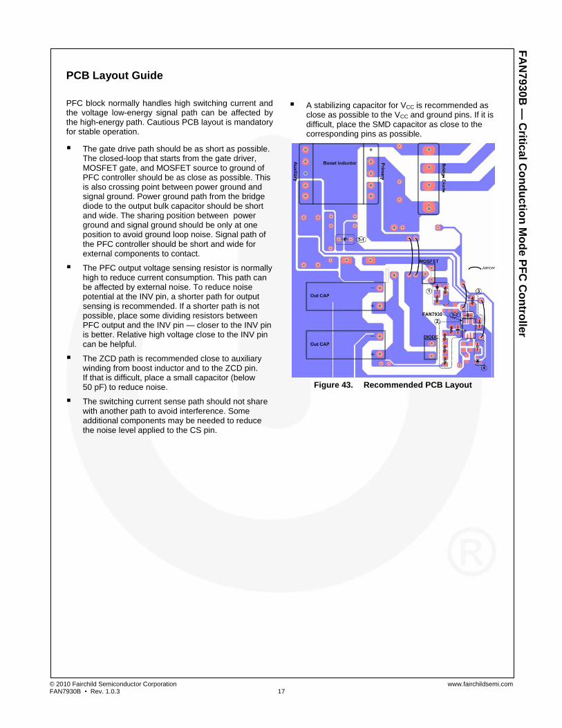
PCB Layout Guide
PFC block normally handles high switching current and the voltage low-energy signal path can be affected by the high-energy path. Cautious PCB layout is mandatory for stable operation.
The gate drive path should be as short as possible. The closed-loop that starts from the gate driver, MOSFET gate, and MOSFET source to ground of PFC controller should be as close as possible. This is also crossing point between power ground and signal ground. Power ground path from the bridge diode to the output bulk capacitor should be short and wide. The sharing position between power ground and signal ground should be only at one position to avoid ground loop noise. Signal path of the PFC controller should be short and wide for external components to contact.
The PFC output voltage sensing resistor is normally high to reduce current consumption. This path can be affected by external noise. To reduce noise potential at the INV pin, a shorter path for output sensing is recommended. If a shorter path is not possible, place some dividing resistors between PFC output and the INV pin — closer to the INV pin is better. Relative high voltage close to the INV pin can be helpful.
The ZCD path is recommended close to auxiliary winding from boost inductor and to the ZCD pin. If that is difficult, place a small capacitor (below 50 pF) to reduce noise.
The switching current sense path should not share with another path to avoid interference. Some additional components may be needed to reduce the noise level applied to the CS pin.
A stabilizing capacitor for VCC is recommended as close as possible to the VCC and ground pins. If it is difficult, place the SMD capacitor as close to the corresponding pins as possible.
Figure 43. Recommended PCB Layout
© 2010 Fairchild Semiconductor Corporation www.fairchildsemi.com FAN7930B • Rev. 1.0.3 18
FA
N7
93
0B
— C
ritica
l Co
nd
uctio
n M
od
e P
FC
Co
ntro
ller
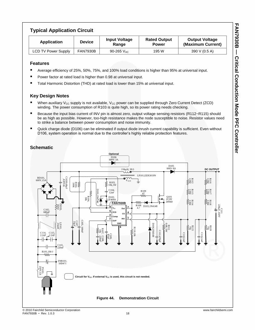
Typical Application Circuit
Application Device Input Voltage
Range Rated Output
Power Output Voltage
(Maximum Current)
LCD TV Power Supply FAN7930B 90-265 VAC 195 W 390 V (0.5 A)
Features
Average efficiency of 25%, 50%, 75%, and 100% load conditions is higher than 95% at universal input.
Power factor at rated load is higher than 0.98 at universal input.
Total Harmonic Distortion (THD) at rated load is lower than 15% at universal input.
Key Design Notes
When auxiliary VCC supply is not available, VCC power can be supplied through Zero Current Detect (ZCD) winding. The power consumption of R103 is quite high, so its power rating needs checking.
Because the input bias current of INV pin is almost zero, output voltage sensing resistors (R112~R115) should be as high as possible. However, too-high resistance makes the node susceptible to noise. Resistor values need to strike a balance between power consumption and noise immunity.
Quick charge diode (D106) can be eliminated if output diode inrush current capability is sufficient. Even without D106, system operation is normal due to the controller’s highly reliable protection features.
Schematic
ZNR101,10D471
194H, 39:5
D105600V 8A
VAUX
DC OUTPUT
Q101FCPF20N60
D106600V 3A
FS
101,
250V
,5A
R101,1M-J
C101,220nF
C114,2.2nF
LF
101,
23m
H
C102,680nF
TH
101,
5D
15
BD101,600V,15A
C1030,6
8
F,6
30
Vdc
C107,
33
F
C105, 1
00nF
R107,
10k
C108,
220nF
C109,
47nF
R110,1
0k
R10947
R1084.7
D103,1N4148
D104,1
N4148
C112,4
70pF
R111
0.0
8, 5
W
C110,1
nF
R115
75k
R112
3.9
M
C111
220
F, 4
50V
LP101,EER3019N
R113
3.9
MR
114
3.9
M
R104,
30k
1
7
6
8
5
2
FAN7930B
CompINV
VCC Out
GND
ZCDCS
OVP
43
C115,2.2nF
R103,10k,1W
D102,UF4004
C104,12nF
D101,1
N4746
R102,
330k
Circuit for VCC. If external VCC is used, this circuit is not needed.
Optional
C116,1
nF
R119
75k
R116
3.9
MR
117
3.9
MR
118
3.9
M
Figure 44. Demonstration Circuit
© 2010 Fairchild Semiconductor Corporation www.fairchildsemi.com FAN7930B • Rev. 1.0.3 19
FA
N7
93
0B
— C
ritica
l Co
nd
uctio
n M
od
e P
FC
Co
ntro
ller
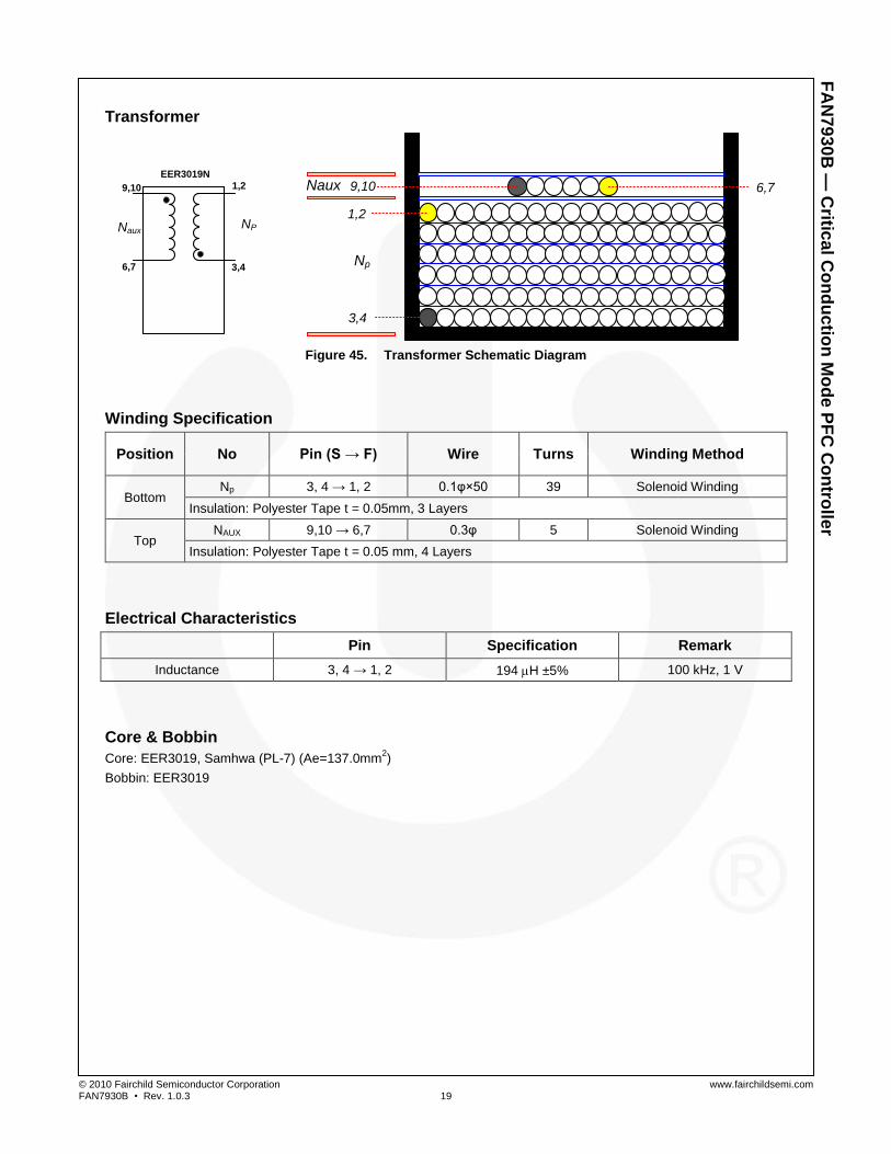
Transformer
1,2
Np
Naux 9,10 6,7
3,4
EER3019N
9,10
6,7
1,2
3,4
NPNaux
Figure 45. Transformer Schematic Diagram
Winding Specification
Position No Pin (S → F) Wire Turns Winding Method
Bottom Np 3, 4 → 1, 2 0.1φ×50 39 Solenoid Winding
Insulation: Polyester Tape t = 0.05mm, 3 Layers
Top NAUX 9,10 → 6,7 0.3φ 5 Solenoid Winding
Insulation: Polyester Tape t = 0.05 mm, 4 Layers
Electrical Characteristics
Pin Specification Remark
Inductance 3, 4 → 1, 2 194 H ±5% 100 kHz, 1 V
Core & Bobbin
Core: EER3019, Samhwa (PL-7) (Ae=137.0mm2)
Bobbin: EER3019
© 2010 Fairchild Semiconductor Corporation www.fairchildsemi.com FAN7930B • Rev. 1.0.3 20
FA
N7
93
0B
— C
ritica
l Co
nd
uctio
n M
od
e P
FC
Co
ntro
ller
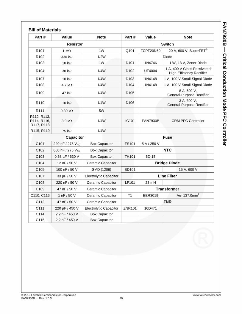
Bill of Materials
Part # Value Note Part # Value Note
Resistor Switch
R101 1 MW 1W Q101 FCPF20N60 20 A, 600 V, SuperFET®
R102 330 kW 1/2W Diode
R103 10 kW 1W D101 1N4746 1 W, 18 V, Zener Diode
R104 30 kW 1/4W D102 UF4004 1 A, 400 V Glass Passivated
High-Efficiency Rectifier
R107 10 kW 1/4W D103 1N4148 1 A, 100 V Small-Signal Diode
R108 4.7 kW 1/4W D104 1N4148 1 A, 100 V Small-Signal Diode
R109 47 kW 1/4W D105
8 A, 600 V, General-Purpose Rectifier
R110 10 kW 1/4W D106
3 A, 600 V, General-Purpose Rectifier
R111 0.80 kW 5W
R112, R113, R114, R116, R117, R118
3.9 kW 1/4W IC101 FAN7930B CRM PFC Controller
R115, R119 75 kW 1/4W
Capacitor Fuse
C101 220 nF / 275 VAC Box Capacitor FS101 5 A / 250 V
C102 680 nF / 275 VAC Box Capacitor NTC
C103 0.68 µF / 630 V Box Capacitor TH101 5D-15
C104 12 nF / 50 V Ceramic Capacitor Bridge Diode
C105 100 nF / 50 V SMD (1206) BD101 15 A, 600 V
C107 33 µF / 50 V Electrolytic Capacitor Line Filter
C108 220 nF / 50 V Ceramic Capacitor LF101 23 mH
C109 47 nF / 50 V Ceramic Capacitor Transformer
C110, C116 1 nF / 50 V Ceramic Capacitor T1 EER3019 Ae=137.0mm2
C112 47 nF / 50 V Ceramic Capacitor ZNR
C111 220 µF / 450 V Electrolytic Capacitor ZNR101 10D471
C114 2.2 nF / 450 V Box Capacitor
C115 2.2 nF / 450 V Box Capacitor
© 2010 Fairchild Semiconductor Corporation www.fairchildsemi.com FAN7930B • Rev. 1.0.3 21
FA
N7
93
0B
— C
ritica
l Co
nd
uctio
n M
od
e P
FC
Co
ntro
ller
Physical Dimensions
Figure 46. 8-Lead, Small Outline Package (SOP)
Package drawings are provided as a service to customers considering Fairchild components. Drawings may change in any manner without notice. Please note the revision and/or date on the drawing and contact a Fairchild Semiconductor representative to verify or obtain the most recent revision. Package specifications do not expand the terms of Fairchild’s worldwide terms and conditions, specifically the warranty therein, which covers Fairchild products. Always visit Fairchild Semiconductor’s online packaging area for the most recent package drawings: http://www.fairchildsemi.com/dwg/M0/M08A.pdf.
8°0°
SEE DETAIL A
NOTES: UNLESS OTHERWISE SPECIFIED
A) THIS PACKAGE CONFORMS TO JEDEC
MS-012, VARIATION AA.
B) ALL DIMENSIONS ARE IN MILLIMETERS.
C) DIMENSIONS DO NOT INCLUDE MOLD
FLASH OR BURRS.
D) LANDPATTERN STANDARD: SOIC127P600X175-8M.
E) DRAWING FILENAME: M08Arev14
F) FAIRCHILD SEMICONDUCTOR.
LAND PATTERN RECOMMENDATION
SEATING PLANE
C
GAGE PLANE
x 45°
DETAIL ASCALE: 2:1
PIN ONE
INDICATOR
4
8
1
B5
A
5.60
0.65
1.75
1.27
6.205.80
3.81
4.003.80
5.004.80
(0.33)1.27
0.510.33
0.25
0.10
1.75 MAX0.25
0.19
0.36
0.500.25
R0.10
R0.10
0.90
0.40(1.04)
OPTION A - BEVEL EDGE
OPTION B - NO BEVEL EDGE
0.25 C B A
0.10
© 2010 Fairchild Semiconductor Corporation www.fairchildsemi.com FAN7930B • Rev. 1.0.3 22
FA
N7
93
0B
— C
ritica
l Co
nd
uctio
n M
od
e P
FC
Co
ntro
ller