factors effecting field emission from multiwalled carbon
TRANSCRIPT

Louisiana State UniversityLSU Digital Commons
LSU Master's Theses Graduate School
2005
Factors effecting field emission from multiwalledcarbon nanotubesAbhilash KrishnaLouisiana State University and Agricultural and Mechanical College
Follow this and additional works at: https://digitalcommons.lsu.edu/gradschool_theses
Part of the Electrical and Computer Engineering Commons
This Thesis is brought to you for free and open access by the Graduate School at LSU Digital Commons. It has been accepted for inclusion in LSUMaster's Theses by an authorized graduate school editor of LSU Digital Commons. For more information, please contact [email protected].
Recommended CitationKrishna, Abhilash, "Factors effecting field emission from multiwalled carbon nanotubes" (2005). LSU Master's Theses. 2854.https://digitalcommons.lsu.edu/gradschool_theses/2854
FACTORS EFFECTING FIELD EMISSION FROM MULTIWALLED CARBON NANOTUBES
A Thesis
Submitted to the Graduate Faculty of the Louisiana State University and
Agricultural and Mechanical College in partial fulfillment of the
requirements for the degree of Master of Science in Electrical Engineering
in
The Department of Electrical and Computer Engineering
by Abhilash Krishna
B.Tech., Jawaharlal Nehru Technological University, Hyderabad, India, 2002
December, 2005

ii
DEDICATION
To my parents and teachers for their love, encouragement & criticism.

iii
ACKNOWLEDGEMENTS
I would like to express my sincere thanks to all persons who directly or indirectly
contributed to completion of my study here at Louisiana State University.
I would like to express my sincere gratitude and respect to my major professor, Dr.
Bingqing Wei for his technical guidance and support. His constructive criticism and advice are
gratefully acknowledged. I am thankful to the committee members, Dr. Pratul Ajmera, Mr.
David Gerez and Dr. Daniels-Race for giving their valuable time to serve in the examination
committee.
I would also like to thank all my colleagues at Center for Advanced Microstructures &
Devices at Louisiana State University, Timothy M. Welborn and Victor Ramirez in particular for
their suggestions and help. I would like to thank Jeong Tae Ok and Charan Masarapu for their
co-operation.
Partial support for this work is received from Schlumberger Technology Corporation and
Louisiana Board of Regents. Any opinions, findings and conclusions or recommendations
expressed here are those of the author and do not necessarily reflect the views of Schlumberger
Limited. The author sincerely acknowledges their support. Author acknowledges financial
support from the Center for Advanced Microstructures & Devices at LSU and Louisiana Board
of Regents.

iv
TABLE OF CONTENTS ACKNOWLEDGEMENTS........................................................................................................... iii LIST OF TABLES......................................................................................................................... vi LIST OF FIGURES ...................................................................................................................... vii SYMBOLS AND CONVENTION USED ..................................................................................... x ABSTRACT................................................................................................................................... xi 1. INTRODUCTION ...................................................................................................................... 1
1.1 Background............................................................................................................................1 1.2 Literature Review: Factors that Affect Field Emission from CNTs ......................................6
1.2.1 Temperature of the CNT................................................................................................ 6 1.2.2 Ambient Pressure of the Surrounding Gas During Field Emission ............................... 7 1.2.3 Type of Ambient Gas Environment............................................................................. 10 1.2.4 Type, Alignment, Inter-tube Spacing, Cap-structure and Geometry of the CNTs ...... 11 1.2.5 Type of Substrate Material Used for CNT Growth ..................................................... 17 1.2.6 Conditions During CNT Growth ................................................................................. 17 1.2.7 Device Configuration................................................................................................... 19 1.2.8 Source Used for CNT Synthesis .................................................................................. 20 1.2.9 Surface Treatment – Gas Exposure.............................................................................. 22 1.2.10 Doping........................................................................................................................ 23
1.3 Scope of Work .....................................................................................................................24 1.4 Organization of Thesis.........................................................................................................26
2. EXPERIMENTAL SYSTEM DESIGN AND AUTOMATION.............................................. 28
2.1 Overview of the System.......................................................................................................28 2.2 Design of the System ...........................................................................................................29 2.3 Safety Measures Incorporated..............................................................................................31 2.4 Automation Using Labview 7.0...........................................................................................32 2.5 Advantages of the Field Emission Experimental System Designed....................................35
3. MWNT SYNTHESIS & CHARACTERIZATION.................................................................. 37
3.1 Microfabrication ..................................................................................................................37 3.1.1 Lithography.................................................................................................................. 37 3.1.2 Mask Preparation ......................................................................................................... 42
3.2 CNT Synthesis – Thermal Chemical Vapor Deposition......................................................43 3.3 Electron Microscopy of CNTs Grown.................................................................................45
4. FACTORS EFFECTING FIELD EMISSION FROM MULTIWALLED CARBON NANOTUBES: RESULTS & OBSERVATIONS ....................................................................... 47
4.1 Effect of CNT Temperature Variation.................................................................................48 4.2 Effect of Background Pressure Variation ............................................................................53
v
4.3 Dependence on the Background Gas Species......................................................................58 4.4 Dependence on CNT Orientation (Random Vs Aligned) ....................................................59 4.5 Effect of the Substrate Material Used for Growth ...............................................................62 4.6 Other Experimental Observations........................................................................................64
4.6.1 CNT Emitter Degradation............................................................................................ 64 4.6.2 Anode Degradation and Heating as a Result of Field Emission.................................. 66 4.6.3 Young’s Interference Fringes ...................................................................................... 68
5. CONCLUSION AND SUGGESTIONS FOR FUTURE RESEARCH.................................... 70
5.1 Summary and Conclusions ..................................................................................................70 5.2 Prospects & Limitations.......................................................................................................71 5.3 Suggested Enhancements in the Experimental System .......................................................72 5.4 Suggestions for Future Research .........................................................................................73
REFERENCES ............................................................................................................................. 75 APPENDIX A: EXPERIMENTAL SYSTEM AUTOMATION USING LABVIEW................. 80 APPENDIX B: TOOLS FOR DATA ANALYSIS DEVELOPED USING MATLAB............... 87 APPENDIX C: PERMISSION TO USE COPYRIGHTED MATERIAL ................................... 95 VITA........................................................................................................................................... 107

vi
LIST OF TABLES 1.1 The Experimental Parameters for CNT Synthesized by Arc Discharge Method. ...................21 2.1 System Capabilities..................................................................................................................30
vii
LIST OF FIGURES 1.1 Potential-energy diagram illustrating the effect of an external electric field on the energy barrier for electrons at a metal surface. )(xV is the one-dimensional potential energy of an electron as a function of its distance x (in Å) from the metal surface. φ is the work function and
pV is the potential energy of the electron inside the metal. E is the local electric field at the surface. .............................................................................................................................................2 1.2 Emitted current versus time (I-t) for an applied voltage of 3 kV during a heating-cooling cycle of 0 to 700 ºC all other conditions remaining the same..........................................................7 1.3 A typical emission pattern of a Multiwalled CNT.....................................................................9 1.4 Direct observation of the ion pumping effect in a sealed field emission display. As soon as the device is turned on, the package pressure drops rapidly..........................................................10 1.5 Measured emission current density vs. applied electric field plotted for a variety of CNT emitters and nanostructured diamond. ...........................................................................................12 1.6 Schematics illustrating the different geometries of macroscopic CNT field emission cathodes and images of the actual CNT structures fabricated. In the ideal case (top), the CNTs are aligned in the field direction and well-spaced (S/H > 1) so that there is less electrical screening ............14 1.7 Cartoon of an anode 10 um above a carbon nanotube showing field enhancement at the electrode surfaces. The potential distribution is given in (a) with each band denoting 5 V potential change. The voltage distribution in the gap is given in (b) with the corresponding field distribution in the inset. (c) results showing decreasing emission threshold field with increasing CNT bundle length.........................................................................................................................16 1.8 (a) The jL–F characteristics of four typical SWNTs. The zigzag (12, 0) and chiral (12, 3) SWNTs are metallic and the chiral (12, 1) and (12, 10) SWNTs are semi conducting. The line densities of currents vs. the chiral vector Ch= (12, m) of SWNTs from m=0 to m=12 are also shown in the inset. (b) The FN plots for the four SWNTs and their derivative sFN =d ln (jL /F2)/d (1/F) (inset)..........................................................................................................................17 1.9 (a) Emission pattern of MPECVD-grown FEA with 20 mA at 4.1 V/ mm. (b) Rise and fall sweeps of the MPECVD-grown CNT–FEA are not obtained due to the vacuum breakdown. (c) Uniform emission pattern of the thermal CVD-grown CNT–FEA with 2 mA at 4.25 V/ mm. (d) Rise and fall sweeps of the thermal CVD FEA show lower turn-on voltage than that of MPECVD-grown CNT–FEA.........................................................................................................18 1.10 (a): Diode Configuration. (b): Triode configuration. (c): Electric field distribution and electron trajectories on a CNT cathode [CNT cathode (bottom), field distribution on the cathode (middle), and trajectories of emitted electrons from the cathode to the anode (top)]....................20 1.11 Field emission characteristics of CNT specimens .................................................................21
viii
1.12 The F–N plots in terms of different gas species and exposure times. The F–N plots with the rise and fall sweeps for (a) N2, (b) O2, and (c) H2 show the hysteresis .......................................22 1.13 Schematic showing scope of work involved in this thesis.....................................................25 2.1 Design of the field emission experimental system. .................................................................30 2.2 Experimental set up..................................................................................................................31 2.3 Two back to back diodes and a series resistor used to protect the pico-ammeter ...................32 2.4 The graphical program written for system automation............................................................33 2.5 Labview User Interface showing the plot of current )(I versus Voltage )(V and also the Fowler-Nordheim plot drawn for )/ln( 2VI versus )/1( V ..............................................................35 3.1 A single block of CNT islands showing the two variable parameters Island size & Inter-island space. ...................................................................................................................................37 3.2 The Lift-off process for patterning SiO2 ..................................................................................38 3.3 An example of mask used for the liftoff process. ....................................................................40 3.4 The Metal Etching process for patterning SiO2 ......................................................................41 3.5 Schematic sketch of the CVD apparatus consisting of a silica tube furnace connected to a vacuum system...............................................................................................................................44 3.6 (a) Islands of CNT Grown over patterned SiO2 (b) A Single Island of Carbon Nanotube (c) Cross-sectional view of the CNT grown........................................................................................46 3.7 TEM image showing the microstructure of the MWNT..........................................................46 4.1 A simplified sketch showing the test fixture used for the experiments. ................................. 47 4.2 Dependence of Field Emitted Current from Multi-Walled Carbon Nanotubes on its temperature. .................................................................................................................................. 49 4.3 Change in Fermi level with rise in temperature of a doped semiconductor [1]...................... 50 4.4 The intensity of the spots on a phosphor screen due to field emission is observed to increase with temperature. From reference [28] with permission (Appendix: C9). ................................... 52 4.5 Variation of current Density with temperature showing saturation at high temperature........ 52 4.6 Effect of change in background pressure of Nitrogen on field emitted current. (fig. contd.). 54

ix
4.7 Effect of change in background pressure of Helium on field emitted current........................ 56 4.8 Effect of change in background pressure of Argon on field emitted current.......................... 57 4.9 Effect of change in background gas species on field emitted current. (fig. contd.)................ 58 4.10 (a) Random and (b) Aligned CNT tested for field emission................................................. 60 4.11 Effect of CNT alignment on field emitted current................................................................ 61 4.12 Effect of the type of substrate on field emitted current. ....................................................... 63 4.13 Few of the imprints on the anode surface disappear after each experiment owing to CNT degradation.................................................................................................................................... 64 4.14 SEM picture showing emitter degradation as a consequence of field emission. The picture shows the region on the substrate where the CNTs have been uprooted...................................... 65 4.15 (a) Imprint observed on the copper anode after field emission (b) Visualization of ring pattern on anode observed by Walker et al.[45]. .......................................................................... 66 4.16 Damaged surface of a gold plated quartz anode. .................................................................. 67 4. 17 Typical Field emission microscope (FEM) image of a MWNT during field emission. From reference [47] with permission (Appendix: C10). ........................................................................ 68 4. 18 Young’s interference fringes found on the anode surface ................................................... 69 5.1 a linear motion feed-through from Huntington Mechanical Laboratories, Inc.that could be used for precise control of inter-electrode spacing. .......................................................................73

x
SYMBOLS AND CONVENTION USED • E : Local Electric field •γ : Field enhancement factor • CNT: Carbon nanotube • FE: Field Emission • MWNT: Multi walled carbon nanotube • SWNT: Single Walled Carbon nanotube • onV : Turn on voltage • thV : Threshold voltage • pV : Potential energy on an electron inside the metal •φ : Work function • e : Charge of an electron •ζ : Fermi energy level •U : Total energy of the electron •W : x -part of the total energy • em : mass of an electron • x : distance from the emitter surface • xP : momentum of the electron in x-direction • J : Field emission current density • I : Field emission current • K : Boltzmann constant •T : Absolute temperature • h : Planck’s constant • A : Field emitting area in the first approximation • Z : Atomic Number • ionE : Ionization Energy •θ : Scattering Angle • :Ω Solid Angle • 0θ : Screening Angle • c : Velocity of light in vacuum • λ : Wavelength •ν : Electron Velocity • kinE : Kinetic energy of an electron

xi
ABSTRACT
Carbon nanotubes (CNT) have emerged to be one of the most versatile of materials ever
discovered. The small dimensions, high electrical conductivity and strength along with other
physical and electrical properties make them a unique material with a wide range of promising
applications. One such use is that of CNTs as electron beam sources.
A typical CNT has a diameter of only a few nanometers but can be hundreds of microns
long. Applying a voltage across the length of such an object results in field emission of electrons
from one end of the tube. This effect is due to intense electric field enhancement that occurs at
the ultra sharp tip of the nanotube. A viable field emission electron beam source can be
fabricated from CNTs.
The primary goal of this work is to study the effects of various factors that influence field
emission from multiwalled CNTs. For the set of factors that was chosen for investigation, a
suitable field emission testing system was designed and assembled. Temperature of the CNTs
was observed to have a considerable effect on the field emission from CNTs. Current saturation
is observed at high temperatures. These findings can prove to be critical if the field emission
device is operating in conditions of high temperature. The effects of variation in ambient
pressure and changes in the background gas species are also studied. The field emission device
characteristic is found to be very sensitive to the ambient gas pressure and more so when the gas
species used was helium. Among Ar, He and N2, it is observed that He is the most suitable for
field emission based device applications. It has been experimentally proven that aligned CNTs
are far superior to random CNTs in terms of field emission characteristics. Effect of different
substrate materials on field emission has also been examined. It has been found that metallic
substrates like stainless steel show promise of better performance. CNT growth conditions have

xii
also been shown to influence their field emission property. Young’s interference fringes found
on the copper anode surface after field emission have been reported here. Emitter and anode
degradation as a result of field emission have been discussed as part of this wok. However it is
important to note that CNTs are relatively more robust and less prone to degradation when
compared to many other conventional field emitters. These results can be applied to find a set of
optimal parameters that could be used for any field emission device design in order to get
maximum field emitted current density at low operating voltages.
1
1. INTRODUCTION
Carbon nanotubes (CNTs) have many exceptional properties that make them attractive
for a variety of applications. In particular, previous work has shown that CNTs can have
outstanding electrical field emission properties, with high emission currents at low electric field
strengths. CNTs are hence attractive as cold-cathode field emission sources, especially for
applications requiring high current densities (hundreds to thousands of amperes per cm2) and
lightweight packages. Recently, there have been numerous fundamental works on optimization
of field emission from CNTs. However, achieving high current densities over large sample areas
of CNTs with repeatability and emission longevity still remains an open problem. This is mainly
due to the fact that field emission from CNTs depends on a wide range of factors which span
from conditions during the CNT growth to the conditions during the field emission operation. To
comprehend how these various factors affect field emission, it is extremely crucial to understand
the basic physics that governs field emission.
1.1 Background
• Principle governing field emission
Field emission is the extraction of electrons from a solid material by tunneling through the
surface-potential barrier under the influence of a strong external electric field. The potential
barrier is rectangular when no electric field is present, and becomes triangular when a negative
potential is applied to the solid. The slope of the latter depends on the amplitude of the local
electric field E just above the surface. This local electric field is drastically enhanced if the
structure of the emitter is very sharp and protruding (High Aspect Ratio) as in the case of a CNT.
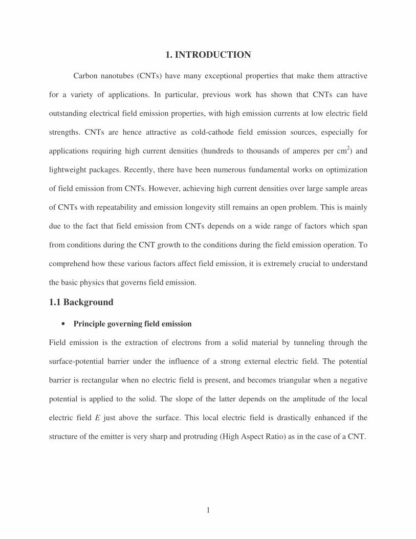
2
Fig. 1.1 Potential-energy diagram illustrating the effect of an external electric field on the energy barrier for electrons at a metal surface. )(xV is the one-dimensional potential energy of an electron as a function of its distance x (in Å) from the metal surface. φ is the work function and
pV is the potential energy of the electron inside the metal. E is the local electric field at the surface [1].
• Fowler-Nordheim Model
The Fowler-Nordheim Model [1] describing the electron emission from metals into a
region of high electric field in vacuum is framed based on the following assumptions:
1) The temperature of the metal is 0 °K.
2) The free-electron approximation applies inside the metal.
3) The surface is considered to be smooth (any irregularities that are present are negligible
compared to the width of the potential barrier) and plane.
4) The potential barrier close to the surface in the vacuum region consists of an image-force
potential and a potential due to the applied external electric field.
3
The image force is a columbic force of attraction pulling the electron emitted towards the
surface due to its induced charge inside the metal. It can be observed from the Fig.1.1 that the net
potential energy of the electron is a result of the summation of the image force potential and the
potential due to the applied external electric field at the surface.
The potential energy of the electron can be given as:
For x < 0 as pVxV =)( (1.1)
And for x > 0 as eExx
exV −
∈−=
°π4)(
2
(1.2)
Where e is the magnitude of charge of the electron and E the electric field strength. As V(x) = 0
at the vacuum level the numerical values of Fermi level ζ and pV are negative. A discontinuity
occurs at the Metal-Vacuum boundary. The fowler Nordheim model for field emission is based
on tunneling of electrons through a one dimensional potential barrier as shown in the Fig.1.1.
U is the total energy of the electron and W is the x -component of the total energy.
)(2
2
xVmP
We
x += (1.3)
xP is the momentum of the electron in the x -direction and em is the mass of the electron.
In this model an assumption is made that only W determines the penetration probability of the
potential barrier by an electron.
The Fowler-Nordheim equation gives a relationship between the emission current
density J , the electric field strength E and the work functionφ . The supply function dWWN )(
equals the number of electrons with the x -component of their energy within the range W to
dWW + incident on the surface per unit area and time. This supply function is multiplied by the
energy dependant probability for barrier penetration )(WD . The number of electrons P(W) in the
4
range W to dWW + tunneling from the metal into the vacuum region is usually called the
normal energy distribution:
dWWDWNdWWP )()()( = (1.4)
The Fowler-Nordheim Equation is found by integrating over all values of W :
∞
=pV
dWWPeJ )( (1.5)
Though it is true that electrons escape from the metal as a result of field emission it is
assumed that the equilibrium of electrons inside the metal is not disturbed. The supply function is
derived from the Fermi-Dirac energy distribution.
The probability for barrier penetration )(WD is found by solving the Schrödinger
equation, substituting for the potential energy )(xV as given in (1.2). Wentzel-Kramer-Brillouin
(WKB) approximation, valid only for the condition when the x-component of the total energy
)(max xVW << is applied. )(max xV is the maximum potential energy of the electron in the
vacuum region. It is assumed that all the electrons penetrating the barrier originate in the
neighborhood of the Fermi level.
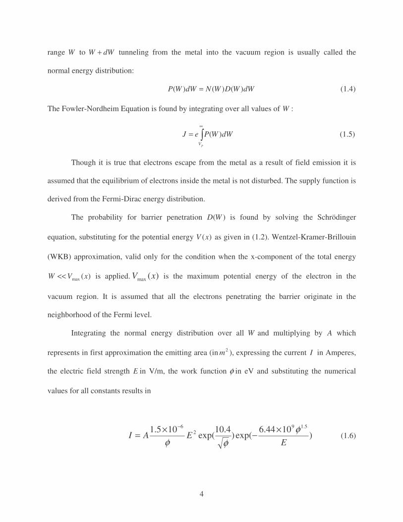
Integrating the normal energy distribution over all W and multiplying by A which
represents in first approximation the emitting area (in 2m ), expressing the current I in Amperes,
the electric field strength E in V/m, the work function φ in eV and substituting the numerical
values for all constants results in
)1044.6
exp()4.10
exp(105.1 5.19
26
EEAI
φφφ
×−×=−
(1.6)
5
For Typical values encountered in carbon based emitters
( eVmtoA 1.09.4,1010 21412 ±== −− φ ) tunneling through the surface barrier becomes significant
for fields above ~3 V/nm [2]. Although the Fowler Nordheim model has been originally
developed for flat metallic surfaces at 0 K, it has proven adaptable to describe field emission
from carbon based electron emitters [3].
To reach the field of ~3 V/nm necessary to extract electrons, field emitting structures
with high aspect ratio’s like sharp objects or protrusions on a surface are employed to amplify
the electric field. In that case, the local electric field is not simply dV / the applied voltage, V,
divided by inter-electrode distance, d but is higher by a factor γ , which gives the emitter the
ability to enhance the field and is accordingly termed the field-enhancement factor. γ is a
geometrical parameter that depends on the dimensions and shape of the emitter and on its
surroundings, as well as on the shape and distance of the counter electrode. The Electric field E
at the emitter surface is written as
dV
Eγ= (1.7)
and (1.7) can be re-written as
)1044.6
exp()4.10
exp()(105.1 2
39
226
Vd
dV
AIγ
φφ
γφ
×−×=−
(1.8)
γ is an important parameter for field emission and can be extracted from the Fowler Nordheim
plot, where )/ln( 2VI is plotted against V/1 . Alternatively, γ can be estimated from the
geometry: for nanotubes the models developed for a cylinder of height h terminated by a half
sphere of radius r on a flat surface can be used, which states that
rh /7.0 ×=γ (1.9)
6
When h is far smaller than the interelectrode distance d .
Equation 1.8 shows quantitatively how the field emitted current depends on the applied
voltage, work function of the emitter and the field enhancement factor. These parameters in turn
depend on various conditions like the temperature of the CNT, the ambient pressure of operation,
orientation of CNT (random vs aligned), type of gas environment and many other factors.
1.2 Literature Review: Factors that Affect Field Emission from CNTs
Numerous fundamental works have been carried out to optimize field emission from
CNTs by getting a handle over the various factors that influence it. Hence, before beginning
experimental studies a detailed review of the past work was carried out. An overview of the
various factors that influence field emission from CNTs is outlined here.
1.2.1 Temperature of the CNT
It has been observed by various groups [4,5] that field emission of electrons from metals
like tungsten strongly depend on temperature especially at high temperatures. It has been
reported that at high temperatures a combined effect of field emission as well thermionic
emission results in the net measured current [4]. Dolan et al. reported a change in work function
as a result of a rise in emitter temperature. As observed earlier from Equation 1.8 any change in
the work function of CNTs would translate into a significant change in the field emitted current.
Increased temperature could have an effect on the electrical conductivity of the CNTs depending
on the type of CNTs used. The conductivity of a metallic CNT would decrease as a result of
increased carrier scattering whereas the conductivity of a semi conducting CNT would get
enhanced as a result of more temperature induced carrier generation. This conductivity
modulation could affect field emission. A negative temperature dependent resistance in multi
walled carbon nanotubes (MWNT) has been reported by Peng et al [6]. However if the transport

7
mechanism in the CNT as claimed by some groups [7] is quasi-ballistic then this conductivity
modulation should have minimal affect on field emission characteristics.
The temperature of the CNT is bound to increase as a result of resistive joule heating
during field emission. This being so if the CNTs are forcefully heated this might result in
lowering of the temperature gradient between the CNT base and tip thus minimizing thermally
induced stress gradient which in turn might improve the CNT field emitter lifetime.
The data in Fig.1.2 reported by a group studying growth of CNT characterized by field
emission measurements during CVD [8] shows that there is a definite effect of the CNT
temperature on its field emission characteristics. The CNT grown in this case was a mixture of
both metallic as well as semi-conducting types. Hence experiments were carried out as part of
this thesis work to understand the temperature dependence of field emission from MWNTs.
Fig. 1.2 Emitted current versus time (I-t) for an applied voltage of 3 kV during a heating-cooling cycle of 0 to 700 ºC all other conditions remaining the same. From reference [8] with permission (Appendix: C1). 1.2.2 Ambient Pressure of the Surrounding Gas During Field Emission
The field emission spots were found to be sensitive to adsorbed gas molecules. This
caused an emission change of the particular site where the gas atom was adsorbed [9]. The

8
number of the gas molecules adsorbed depends not only on the emitter surface area but also on
the background ambient pressure of the gas.
Depending on the type of gas the emission change after adsorption may be reversible
after heat treatment of the CNTs. The temperature of the CNT rises as a result of prolonged field
emission which may cause the adsorbed molecules to leave its surface depending on the type of
gas molecule adsorbed.
This phenomenon in-turn influences the uniformity and stability of emission. This
process of alteration of the field emission characteristic due to adsorption and desorption of gas
molecules is attributed to the variation of energy barrier height for field emission at the gas
adsorbed site.
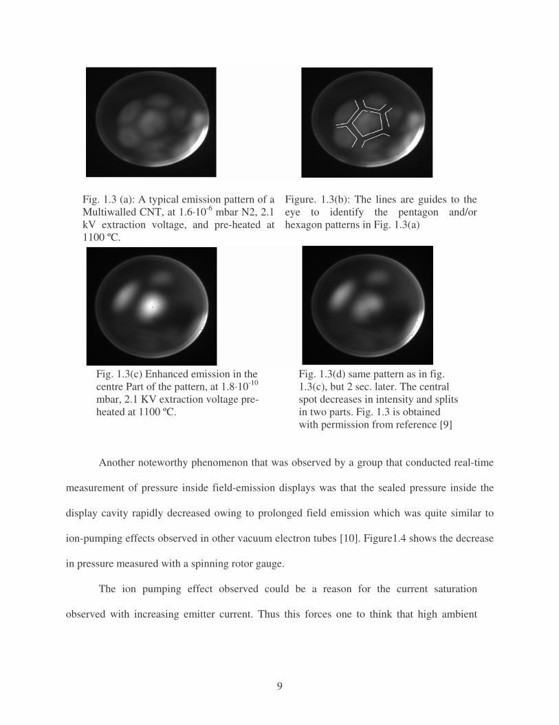
The images shown in fig 1.3 were observed during field emission from a multi walled
carbon nanotube. The images formed on a phosphor screen were recorded in this case using a
CCD camera. It is believed that the adsorbents will be driven to the cap by the field and will alter
the localized state. This not only causes a change in the intensity of the emission but also alters
the geometry of the image obtained. This can be very clearly observed from the Fig. 1.3
This shows the dynamic nature of the surface near the tip of the CNT due to the adsorbed
molecules. The intensity of the field emission spots were observed in this case in an Ultra high
vacuum system with a pressure of 1.8x 10⁻⁸ mbars. It was observed that a clear nanotube emits a
pattern containing pentagons or hexagons. The presence of an adsorbed molecule distorts this
regularity.
9
Fig. 1.3 (a): A typical emission pattern of a Multiwalled CNT, at 1.6·10-6 mbar N2, 2.1 kV extraction voltage, and pre-heated at 1100 ºC.
Figure. 1.3(b): The lines are guides to the eye to identify the pentagon and/or hexagon patterns in Fig. 1.3(a)
Fig. 1.3(c) Enhanced emission in the centre Part of the pattern, at 1.8·10-10 mbar, 2.1 KV extraction voltage pre-heated at 1100 ºC.
Fig. 1.3(d) same pattern as in fig. 1.3(c), but 2 sec. later. The central spot decreases in intensity and splits in two parts. Fig. 1.3 is obtained with permission from reference [9]
Another noteworthy phenomenon that was observed by a group that conducted real-time
measurement of pressure inside field-emission displays was that the sealed pressure inside the
display cavity rapidly decreased owing to prolonged field emission which was quite similar to
ion-pumping effects observed in other vacuum electron tubes [10]. Figure1.4 shows the decrease
in pressure measured with a spinning rotor gauge.
The ion pumping effect observed could be a reason for the current saturation
observed with increasing emitter current. Thus this forces one to think that high ambient
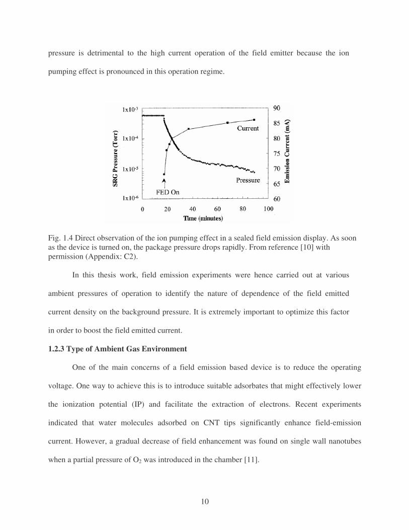
10
pressure is detrimental to the high current operation of the field emitter because the ion
pumping effect is pronounced in this operation regime.
Fig. 1.4 Direct observation of the ion pumping effect in a sealed field emission display. As soon as the device is turned on, the package pressure drops rapidly. From reference [10] with permission (Appendix: C2).
In this thesis work, field emission experiments were hence carried out at various
ambient pressures of operation to identify the nature of dependence of the field emitted
current density on the background pressure. It is extremely important to optimize this factor
in order to boost the field emitted current.
1.2.3 Type of Ambient Gas Environment
One of the main concerns of a field emission based device is to reduce the operating
voltage. One way to achieve this is to introduce suitable adsorbates that might effectively lower
the ionization potential (IP) and facilitate the extraction of electrons. Recent experiments
indicated that water molecules adsorbed on CNT tips significantly enhance field-emission
current. However, a gradual decrease of field enhancement was found on single wall nanotubes
when a partial pressure of O2 was introduced in the chamber [11].

11
Unlike water molecules the presence of oxygen and hydrogen did not appreciably affect
the field emission behavior. It is believed water gets attracted to metallic nanotube tips under
field-emission conditions, and forms complexes that are stable at several hundred degrees above
room temperature [12]. Resulting electrostatic interactions from the adsorbates make the highest
occupied molecular orbital (HOMO) level in the nanotube more unstable, with a corresponding
decrease in the ionization potential. The instability of the HOMO and the lowering of IP are both
enhanced with an increasing number of water molecules adsorbed (up to a saturation density). H2
weakly interacts with the nanotube tip even under field-emission conditions, and is not stable at
room temperatures [12]. As part of this work three gas species He, N2 & Ar were selected to be
used to see if they caused any enhancement in the field emitted current.
1.2.4 Type, Alignment, Inter-tube Spacing, Cap-structure and Geometry of the CNTs
• Type of Carbon Nanotubes (SWNT/MWNT)
SWNT generally have a smaller diameter and higher degree of structural perfection than
MWNTs,and thus SWNTs have the capability of achieving higher current densities and a longer
life time [13]. The diameter of the SWNTs is usually in the range of 1–2 nm while the diameter
of the MWNTs is 20–100 nm. This suggests that the SWNTs have a very high aspect ratio.
This however does not directly translate itself into a very high electric field amplification
factor. The reason for this is that they normally form close-packed bundles comprising 10 to 100
SWNTs with a bundle diameter of 10 –100 nm. Hence the effective bundle diameter decides the
field amplification factor of these emitting structures. It can be seen from Fig 1.5 that the field
emission characteristics of SWNT exhibits lower turn-on voltage when compared to the MWNT.
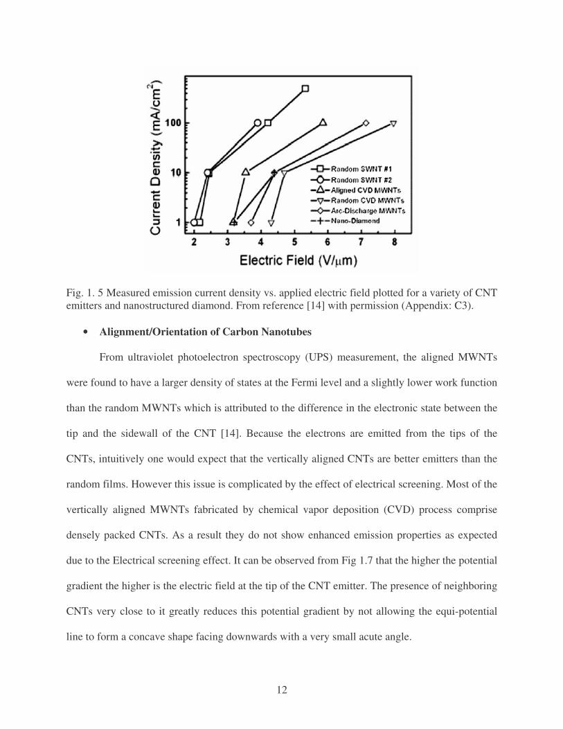
12
Fig. 1. 5 Measured emission current density vs. applied electric field plotted for a variety of CNT emitters and nanostructured diamond. From reference [14] with permission (Appendix: C3).
• Alignment/Orientation of Carbon Nanotubes
From ultraviolet photoelectron spectroscopy (UPS) measurement, the aligned MWNTs
were found to have a larger density of states at the Fermi level and a slightly lower work function
than the random MWNTs which is attributed to the difference in the electronic state between the
tip and the sidewall of the CNT [14]. Because the electrons are emitted from the tips of the
CNTs, intuitively one would expect that the vertically aligned CNTs are better emitters than the
random films. However this issue is complicated by the effect of electrical screening. Most of the
vertically aligned MWNTs fabricated by chemical vapor deposition (CVD) process comprise
densely packed CNTs. As a result they do not show enhanced emission properties as expected
due to the Electrical screening effect. It can be observed from Fig 1.7 that the higher the potential
gradient the higher is the electric field at the tip of the CNT emitter. The presence of neighboring
CNTs very close to it greatly reduces this potential gradient by not allowing the equi-potential
line to form a concave shape facing downwards with a very small acute angle.
13
As shown in Figure 1.5, the emission characteristic of the aligned MWNTs is
significantly different from that of the random MWNT film. By lithographically patterning the
location of the catalysts on the substrates, several groups have recently reported aligned CNTs
and carbon nanofibers with controlled spacing to minimize the screening effects. One concern of
this approach is whether the lifetime of the cathode is affected because of the significant
reduction in the density of the CNTs. For cathodes with randomly oriented CNTs, the emitters
come from two sources. One is the small fraction of the CNTs that point to the current collector
due to simple statistical distribution. The second group comes from field induced alignment.
Several experiments [15,16] have shown the CNTs can be easily bent and aligned to the
electrical field direction under a moderate electrical field. One advantage of this type of cathode
is the large number of CNTs available for emission which can lead to a longer lifetime.
Since lifetime as well as high current extraction are critical factors in deciding the
acceptability of a CNT field emitter, according to our plan, experiments were carried out to
compare a random and a well aligned CNT sample with the same physical layout to see how
orientation affects the field emission current.
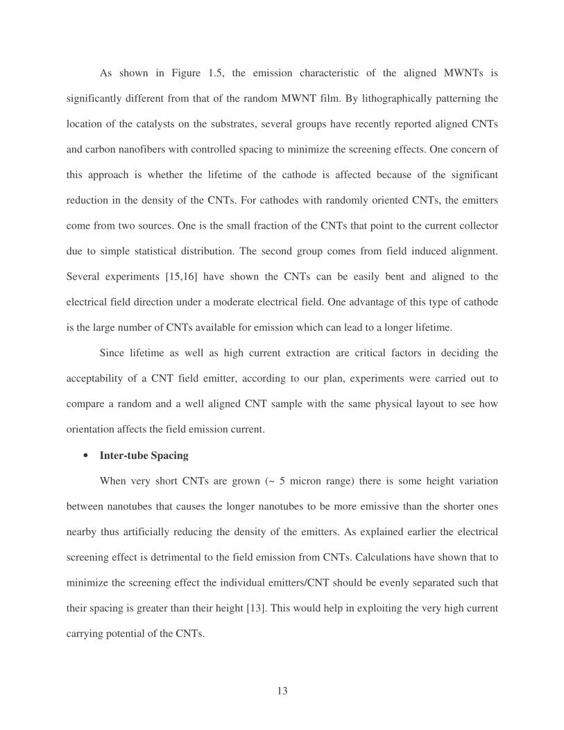
• Inter-tube Spacing
When very short CNTs are grown (~ 5 micron range) there is some height variation
between nanotubes that causes the longer nanotubes to be more emissive than the shorter ones
nearby thus artificially reducing the density of the emitters. As explained earlier the electrical
screening effect is detrimental to the field emission from CNTs. Calculations have shown that to
minimize the screening effect the individual emitters/CNT should be evenly separated such that
their spacing is greater than their height [13]. This would help in exploiting the very high current
carrying potential of the CNTs.
14
Fig. 1.6 Schematics illustrating the different geometries of macroscopic CNT field emission cathodes and images of the actual CNT structures fabricated. In the ideal case (top), the CNTs are aligned in the field direction and well-spaced (S/H > 1) so that there is less electrical screening. From reference [13] with permission (Appendix: C4).
• Structure of the Cap
A theoretical study predicted that an open-ended SWNT has much better field-emission
properties than a closed SWNT [13], due to the electronic effects that alter the bonding mode and
decrease the work function. No experiments have been reported yet on the comparison of open
and closed SWNTs. In the case of a closed-capped MWNTs simulation results showed that the
emission current drastically increases with a small increase in the major radius of the ellipsoidal
tip. For open-ended MWNTs with flat top and round edges the emission current is observed to
depend highly on the sharpness of the edges. The simulation results show that the emission
15
current mostly comes from the outer corner of the flat top and both inner corner and the flat top
plays very little role in the filed emission process [13].
• Structure and geometry of the carbon nanotube
The geometry of the CNT has a direct impact on its field emission properties.
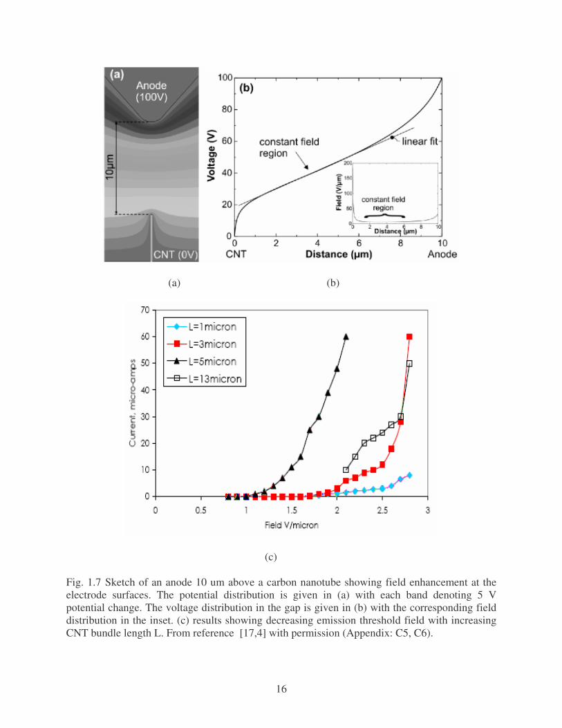
Experimental results show that the emission threshold field increases with decreasing CNT
bundle lengthL as shown in fig.1.7(c). Keeping the diameter of the CNT constant, the
lengthening of the nanotubes which causes an increase in its aspect ratio is observed to provoke
an increase of the emitted current at constant applied voltage because of the increase in the field
enhancement factor.
Fig 1.7(a, b) clearly shows the field enhancement occurring at the tip of the CNT emitter
due to its favorable aspect ratio. It can be observed from the figure that the electric field which is
given by the rate of change of the voltage with distance dxdV / is maximum near the surface of
the emitter. The anomaly observed in Fig1.7(c) when the length of the CNT goes from 5 um to
13 um reiterates the fact that for a given CNT emitter density there is an optimum CNT length to
CNT spacing ratio required to get maximum field emitted current per cm2 all other conditions
remaining the same.
The field emission characteristic is also found to be dependant on the chirality [18] of a
CNT. The chirality of the CNT in turn decides the metallic or the semiconducting nature of the
CNT. A metallic tube has a line density (jL) higher than that of a semiconducting one. The line
density is defined as the current per unit length of the CNT under test. Also, for semiconducting
tubes, a tube of larger chiral angle has a line density higher than that of smaller chiral angle; a
zigzag semiconducting tube has a smallest line density among the others. These facts can be
noted from Fig. 1.8.
16
(a) (b)
(c)
Fig. 1.7 Sketch of an anode 10 um above a carbon nanotube showing field enhancement at the electrode surfaces. The potential distribution is given in (a) with each band denoting 5 V potential change. The voltage distribution in the gap is given in (b) with the corresponding field distribution in the inset. (c) results showing decreasing emission threshold field with increasing CNT bundle length L. From reference [17,4] with permission (Appendix: C5, C6).

17
Fig. 1.8 (a) The line density versus the field strength (jL–F) characteristics of four typical SWNTs. The zigzag (12, 0) and chiral (12, 3) SWNTs are metallic and the chiral (12, 1) and (12, 10) SWNTs are semi conducting. The line densities of currents vs. the chiral vector Ch= (12, m) of SWNTs from m=0 to m=12 are also shown in the inset. (b) The FN plots for the four SWNTs and their derivative sFN =d ln (jL /F2)/d (1/F) (inset). From reference[18] with permission (Appendix: C7). 1.2.5 Type of Substrate Material Used for CNT Growth
Different substrate/base materials on which the CNT is grown would have different
values of resistivity hence would result in different electric field threshold voltages. Nanotubes
can be self doped by the material of the substrate on which it is grown [19]. This would also
affect its field emission characteristics. Hence, a careful study of the dependence of field
emission from CNTs on the substrate material becomes imperative. Different substrate materials
like SiO2, nickel & stainless steel have been tested for field emission.
1.2.6 Conditions During CNT Growth
CNTs can be fabricated in laboratory quantities by several techniques including arc-
discharge, laser ablation and chemical vapor deposition (CVD) [20]. The structure and
morphology of the CNTs fabricated by each technique vary significantly. The arc-discharge and
18
laser-ablation methods use extremely high temperatures – the temperature of the plasma/plume is
3000–4000 C. As a result the CNTs produced tend to have a higher degree of graphitization than
those produced by the CVD process which normally operates at 800–1200 C. The defect density
affects the thermal and electrical conductivity, the mechanical strength of the CNTs and
therefore their emission characteristics due to stable CNT heating and subsequent destruction
during field emission.
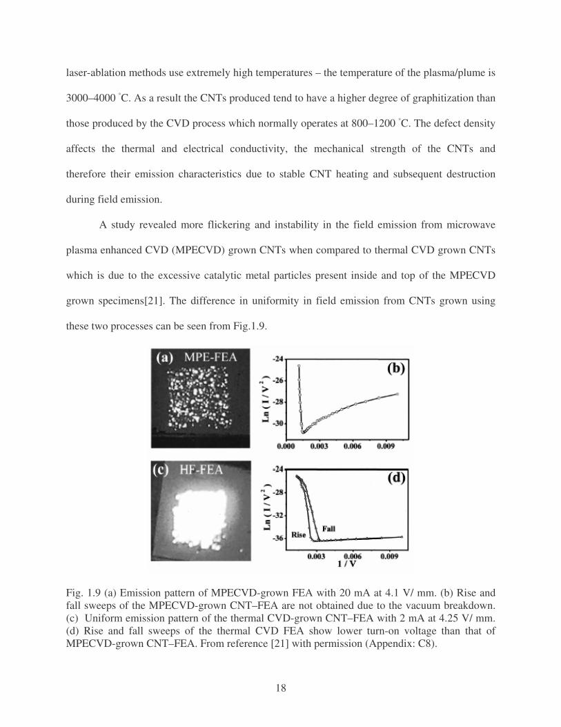
A study revealed more flickering and instability in the field emission from microwave
plasma enhanced CVD (MPECVD) grown CNTs when compared to thermal CVD grown CNTs
which is due to the excessive catalytic metal particles present inside and top of the MPECVD
grown specimens[21]. The difference in uniformity in field emission from CNTs grown using
these two processes can be seen from Fig.1.9.
Fig. 1.9 (a) Emission pattern of MPECVD-grown FEA with 20 mA at 4.1 V/ mm. (b) Rise and fall sweeps of the MPECVD-grown CNT–FEA are not obtained due to the vacuum breakdown. (c) Uniform emission pattern of the thermal CVD-grown CNT–FEA with 2 mA at 4.25 V/ mm. (d) Rise and fall sweeps of the thermal CVD FEA show lower turn-on voltage than that of MPECVD-grown CNT–FEA. From reference [21] with permission (Appendix: C8).
19
Metal particles are very harmful to dependable operation of the field emission array
(FEA) because the melting and evaporation of metal particles by high emission currents abruptly
surge the emission currents and result in vacuum breakdown, followed by the failure of the
CNT–FEA. As part of this work, CNT growth was carried out under normal atmospheric
pressure and in vacuum to compare field emission characteristics in both the cases.
The following factors discussed in sections 1.2.7, 1.2.8, 1.2.9 and 1.2.10 are found to
affect field emission characteristics of CNTs. However their study is beyond the scope of this
work. It has been included here to give the reader a complete picture.
1.2.7 Device Configuration
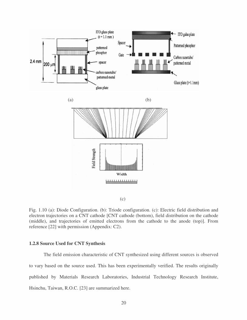
The device configuration decides the collection efficiency of the emitted electrons hence
is a crucial factor to be noted during field emission device design. Due to the strong electric field
enhancement of the edge, trajectory of the emitted electrons is deviated from the center of the
electrode as shown in Fig. 1.10 (c) [22]. The electron deviation could be overcome if a gate
electrode is incorporated between cathode and anode. This forces the need for a triode type of
configuration which facilitates better focusing of the emitted electrons.
Recently a lot of work has been done in designing optimized triode type structures for
assisting electron extraction as shown in Fig. 1.10 (b) however these types of designs suffered
from high leakage currents as a result of the third accelerating electrode.
Having the luxury of a large collector in the sandwiched device structure used for this
work the need for a third focusing electrode is avoided. Hence, a diode type of structure as
shown in Fig. 1.10 (a) is used without compromising on the collector efficiency. This work also
lays a foundation for the realization of a field emission based CNT diode that can be operated in
both forward as well as reverse bias.
20
(a) (b)
(c)
Fig. 1.10 (a): Diode Configuration. (b): Triode configuration. (c): Electric field distribution and electron trajectories on a CNT cathode [CNT cathode (bottom), field distribution on the cathode (middle), and trajectories of emitted electrons from the cathode to the anode (top)]. From reference [22] with permission (Appendix: C2).
1.2.8 Source Used for CNT Synthesis
The field emission characteristic of CNT synthesized using different sources is observed
to vary based on the source used. This has been experimentally verified. The results originally
published by Materials Research Laboratories, Industrial Technology Research Institute,
Hsinchu, Taiwan, R.O.C. [23] are summarized here.
21
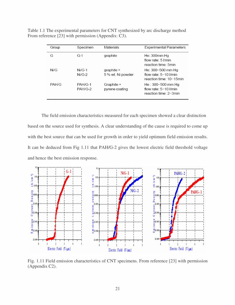
Table 1.1 The experimental parameters for CNT synthesized by arc discharge method From reference [23] with permission (Appendix: C3).
The field emission characteristics measured for each specimen showed a clear distinction
based on the source used for synthesis. A clear understanding of the cause is required to come up
with the best source that can be used for growth in order to yield optimum field emission results.
It can be deduced from Fig 1.11 that PAH/G-2 gives the lowest electric field threshold voltage
and hence the best emission response.
Fig. 1.11 Field emission characteristics of CNT specimens. From reference [23] with permission (Appendix C2).
22
1.2.9 Surface Treatment – Gas Exposure
Gas exposure induces chemi- and physisorption of gas molecules on the surface of CNTs.
As a result of surface treatment the presence of adsorbates is observed to enhance field emission
at low fields and high vacuum conditions [21]. Increasing the field beyond a certain limit
displaces the adsorbates (leading to fluctuations in emission current) and finally removes them. I-
V curves acquired immediately after such a cleaning process is carried out shows higher onset
fields.
Experimental study of the dependence of field emission on gas exposures of CNTs have
been reported by a group which used oxygen, nitrogen and hydrogen for surface treatment of
CNT before carrying out field emission experiments [21]. The results obtained are summarized
below in Fig.1.12.
Fig. 1.12 The F–N plots in terms of different gas species and exposure times. The F–N plots with the rise and fall sweeps for (a) N2, (b) O2, and (c) H2 show the hysteresis. From reference [21] with permission (Appendix: C8).
In the rise bias sweep, the current saturation, indicated by arrows in Fig. 1.12, was
observed and this resulted in two slopes. The current saturation occurred for all gases. A change
in slope of the field emission characteristic due to saturation reflects in the Fowler Nordheim plot
as well which can be seen from the Fig.1.12 The fall bias sweep initially showed only a single
23
slope; in other words, no current saturation. However, after long exposures of oxygen and
nitrogen, current saturations indicated by arrows in Figs. 1.12(a) and 1.12(b) are observed even
in the fall sweep, whereas the degree of saturation in the fall sweep is stronger in oxygen.
However, shown in Fig. 1.12(c), the current saturation in the fall sweep after long hydrogen gas
exposure did not occur, and additionally, the degree of hysteresis was reduced in hydrogen
exposure. This result implied that the role of hydrogen gas is different from oxygen and nitrogen
gases. It is manifested by the shift of F–N plots after each gas exposure. Oxygen and nitrogen
exposures push the F–N plots toward the high voltage region, whereas hydrogen exposures pull
them back to the lower-voltage region.
It is argued that similar tendencies in degradation of the emission properties resulting
from oxygen and nitrogen exposures may be explained by the electronegativity and adsorption
property of gases. Adsorption of materials with high electronegativity is said to hinder the
electron emission by intensifying the local potential barriers [21].
It is believed that hydrogen gas removes adsorbates by bombarding the emitter surface
with energetic hydrogen atoms, which consequently cleans the emitters. Therefore, the current
saturation during the fall sweep at large gas-exposure times from oxygen and nitrogen gases is
not observed from the hydrogen gas exposures. Therefore, hydrogenation of the CNT– FEA has
the technical significance for the activation of the field-emission display, whose performance is
degraded due to other adsorbates. Whereas, oxygen gas is believed to depress the field emission
severely and even change the tip morphology by possible oxidative etching [21].
1.2.10 Doping
As is the case of other carbon allotropes, the electronic properties of the CNTs can be
modified and tuned by chemical doping. Experimentally, it has been shown that the work

24
function of the SWNTs can be reduced to as low as 2.5 eV by intercalation with Cs [13]. Each
alkali metal atom can donate one electron to the SWNT which results in the reduction of the
work function. A recent theoretical calculation shows the same trend as the experimental result
[2]. The effect of Cs intercalation on the field emission properties has also been studied. The
result showed that Cs deposition on SWNTs can decrease the turn-on field by a factor of 2–3 and
increase the emission current [13], consistent with reduction of the electronic work function due
to Cs intercalation. The intercalated CNTs however are air-sensitive and can easily de-intercalate
when the emission current is high.
As explained earlier nanotubes can be self-doped by material of substrate [17]. It is
known that the dopants can have different localization in the MWNT giving different
distributions lengthwise in the nanotube. The dopant site can be in the enclosure of MWNT such
as between their walls or on the surface etc. This could change the electronic structure of
nanotubes and in turn have a consequence on their field emission properties.
To achieve the goal of maximizing the current density at lowest possible threshold
voltage it is necessary to investigate the nature of dependence of the field emitted current over
the various factors discussed here. This need for a detailed study determined the scope of work
carried out as part of this thesis.
1.3 Scope of Work
The spectrum of work that was intended to be carried out and that has been successfully
completed is illustrated in a sequential fashion in Fig. 1.13. The work began with the analysis of
experimental requirements which was followed by the stage of system design and assembly. On
a parallel track Microfabrication and CNT synthesis and treatment was carried out. This was
followed by experimentation. During experimentation problems with manual data recording
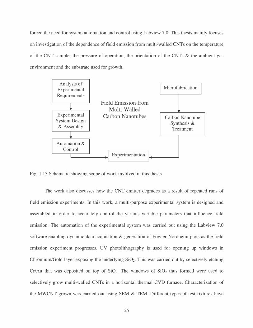
25
forced the need for system automation and control using Labview 7.0. This thesis mainly focuses
on investigation of the dependence of field emission from multi-walled CNTs on the temperature
of the CNT sample, the pressure of operation, the orientation of the CNTs & the ambient gas
environment and the substrate used for growth.
Fig. 1.13 Schematic showing scope of work involved in this thesis
The work also discusses how the CNT emitter degrades as a result of repeated runs of
field emission experiments. In this work, a multi-purpose experimental system is designed and
assembled in order to accurately control the various variable parameters that influence field
emission. The automation of the experimental system was carried out using the Labview 7.0
software enabling dynamic data acquisition & generation of Fowler-Nordheim plots as the field
emission experiment progresses. UV photolithography is used for opening up windows in
Chromium/Gold layer exposing the underlying SiO2. This was carried out by selectively etching
Cr/Au that was deposited on top of SiO2. The windows of SiO2 thus formed were used to
selectively grow multi-walled CNTs in a horizontal thermal CVD furnace. Characterization of
the MWCNT grown was carried out using SEM & TEM. Different types of test fixtures have
Analysis of Experimental Requirements
Experimental System Design
& Assembly
Automation & Control
Experimentation
Microfabrication
Carbon Nanotube Synthesis & Treatment
Field Emission from Multi-Walled
Carbon Nanotubes
26
been used for field emission in order to zero down on the most efficient one in terms of life time
and the obtained field emission current density. Enhancements in the experimental system
designed have been suggested in detail. Among various novel applications pointed out the use of
CNTs as a field emission based diode has been experimentally verified. The main objective is to
determine a set of conditions/parameters that would result in maximum field emission current
density at the lowest possible applied electric field causing least damage to the CNT emitter thus
increasing its lifetime.
1.4 Organization of Thesis
In chapter 1, relevant concepts in theoretical physics governing field emission have been
covered. The Fowler Nordheim model is discussed in detail leading to the derivation of the
Fowler Nordheim equation. The field emission analysis is initially carried out for the case of a
metal emitter and extrapolated to the case of a CNT. The overall scope of this thesis is discussed.
Various factors that affect field emission from CNTs have been highlighted.
In chapter 2 the system that was designed and assembled to carry out field emission
experiments is discussed in detail. Its capabilities and drawbacks are discussed. Details of the
program written for dynamic data acquisition and generation of Fowler-Nordheim plots are
covered.
In chapter 3 the different approaches of microfabrication employed are presented. The
reason for the approach adopted is explained. An overview of the process of CNT synthesis that
is used is discussed. The structure and characteristics of CNT grown as obtained from TEM and
SEM are covered.
In chapter 4 results of various experiments performed are presented. The effect of
temperature, pressure, different ambient gases & physical layout on field emission from CNTs is

27
discussed in detail. The various observations made during experimentation are highlighted with
evidence.
In chapter 5 recommendations for further research are given and conclusions are drawn.
Prospects and limitations of MWNT as a field emission source are discussed. Enhancements to
the current experimental system are submitted. Novel areas of application to CNT field emission
sources are presented. Symbols & conventions used are enlisted on page x.
28
2. EXPERIMENTAL SYSTEM DESIGN AND AUTOMATION
2.1 Overview of the System
The experiments that dictated the design of the field emission system are 1. Recording field emission current from MWNTs as the voltage is incremented in steps from 0
to 5000 V.
2. Measurement of field emission current with varying temperature of the CNT samples. 3. Investigation of the dependence of field emission current on the ambient pressure of operation. 4. Study of the impact of various gases like He, N2 & Ar on field emission from MWNTs.
A high voltage supply that could source any voltage between 0V to 5000 V was required
to be applied across the length of MWNTs to force electrons to be field emitted. Keithley Model
248 high voltage supply was used for this purpose. This had the advantage of possessing a GPIB
interface that could be used to remotely control it.
The turn-on voltage of a CNT field emitter is defined as the applied voltage for which the
field emission current density is equal to10uA/cm2. The typical effective field emitting area
could be as small as10-6cm2. (a square island with a side of length10um). Hence to determine the
turn on voltage of such a field emitting structure a Pico-ammeter was necessary. Keithley 6485
pico-ammeter was used for this purpose. This model also had a GPIB interface for remote
control. The range of measurable current using this instrument is 2nA to 20mA. The resolution
of the reading from the pico-ammeter is of the order of femto-ampere however owing to the
noise level, measurements below nano-ampere could not be achieved.
The second study required a stage whose temperature could be remotely controlled. The
capability desired was to precisely control sub-zero to very high temperatures. A custom
designed stage was built in order to facilitate these temperature dependant measurements. The
design had two stages S1 and S2. S1 could be used to reduce the sample temperature to C°−193 .
29
S2 could be used to heat the sample up to C°1600 . The stage S1 which is a brazed copper
reservoir achieves low temperatures using liquid nitrogen. The stage S2 which is a 2 ′′ BN coated
graphite heater stage achieves high temperature using a resistively heated coil. A programmable
temperature controller allows setting the temperature of both the stages.
The third study forced the need for precise control & monitoring of pressure over a wide
range. This was achieved by using three pressure gauges, an MKS Baratron capacitance
manometer with a range of 10-2T to 10-3T, a Granville-Phillips Convectron gauge with a range of
10-4T to 1 atm and a Kurt J Lesker Bayard Alpert Ion gauge with a range of 10-4T to 10-9T. A
rotary vane mechanical pump in conjunction with an ion pump is used to pump down the
vacuum chamber. The vacuum could be drawn to as low as 10-7T. An MKS Mass Flow
Controller is used to adjust the flow of gas into the chamber in order to stabilize the pressure of
the gas in the vacuum chamber at a specific desired value as the vacuum pump is left to run
continuously. A multi-gauge controller is used to monitor pressure readings from all the three
gauges.
To carry out the fourth function of the experimental system the vacuum chamber is
provided with an inlet for gas. The desired gas is fed into the vacuum chamber from the
respective cylinder through the Mass Flow Controller as explained earlier.
2.2 Design of the System
The Figure 2.1 shows the detailed design of the field emission experimental system
highlighting the various inter-connections. Essentially the high voltage supply, the Pico-ammeter
and the field emission test fixture placed inside the vacuum chamber are connected in series.
Ceramic cased power feed-through is used to carry the high voltage from the power supply into
the chamber. A PC is used for data acquisition from, and control of the high voltage supply and
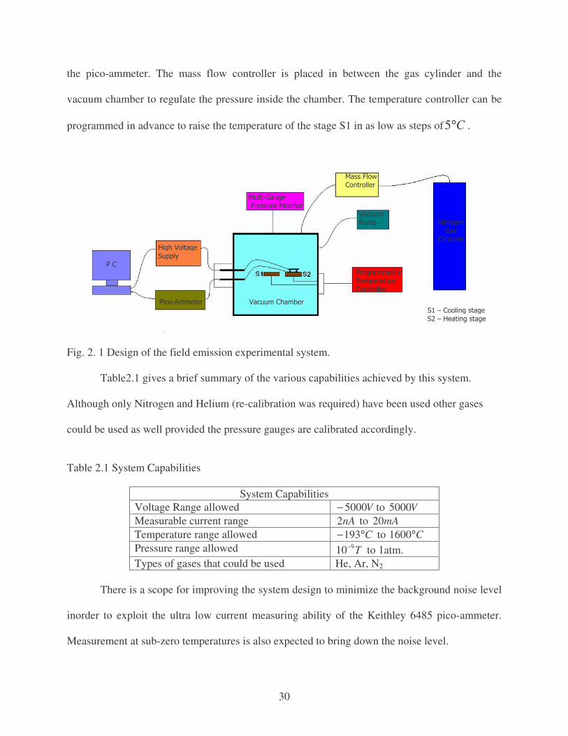
30
the pico-ammeter. The mass flow controller is placed in between the gas cylinder and the
vacuum chamber to regulate the pressure inside the chamber. The temperature controller can be
programmed in advance to raise the temperature of the stage S1 in as low as steps of C°5 .
Fig. 2. 1 Design of the field emission experimental system.
Table2.1 gives a brief summary of the various capabilities achieved by this system.
Although only Nitrogen and Helium (re-calibration was required) have been used other gases
could be used as well provided the pressure gauges are calibrated accordingly.
Table 2.1 System Capabilities
System Capabilities Voltage Range allowed V5000− to V5000 Measurable current range nA2 to mA20 Temperature range allowed C°−193 to C°1600 Pressure range allowed T910− to 1atm. Types of gases that could be used He, Ar, N2
There is a scope for improving the system design to minimize the background noise level
inorder to exploit the ultra low current measuring ability of the Keithley 6485 pico-ammeter.
Measurement at sub-zero temperatures is also expected to bring down the noise level.
!"#"

31
The experimental set up shown in figure 2.2 that was designed and assembled at the
Center for Advanced Microstructures and Devices is totally functional.
Fig. 2.2 Experimental set up. 2.3 Safety Measures Incorporated
A protective circuitry is used to ensure that the pico-ammeter is safe in case the
electrodes inside the vacuum chamber get shorted [24]. Keeping the 2002 National Electrical
Code the entire circuit was designed giving utmost priority to personnel safety. Care has also
been taken to avoid any damage to the equipment being used. This was very important
considering the fact that the experiments performed require operation at high voltage and
reasonably high currents.
32
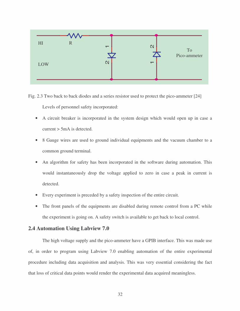
Fig. 2.3 Two back to back diodes and a series resistor used to protect the pico-ammeter [24] Levels of personnel safety incorporated:
• A circuit breaker is incorporated in the system design which would open up in case a
current > 5mA is detected.
• 8 Gauge wires are used to ground individual equipments and the vacuum chamber to a
common ground terminal.
• An algorithm for safety has been incorporated in the software during automation. This
would instantaneously drop the voltage applied to zero in case a peak in current is
detected.
• Every experiment is preceded by a safety inspection of the entire circuit.
• The front panels of the equipments are disabled during remote control from a PC while
the experiment is going on. A safety switch is available to get back to local control.
2.4 Automation Using Labview 7.0
The high voltage supply and the pico-ammeter have a GPIB interface. This was made use
of, in order to program using Labview 7.0 enabling automation of the entire experimental
procedure including data acquisition and analysis. This was very essential considering the fact
that loss of critical data points would render the experimental data acquired meaningless.
12 1
2
HI
LOW
To Pico-ammeter
R
33
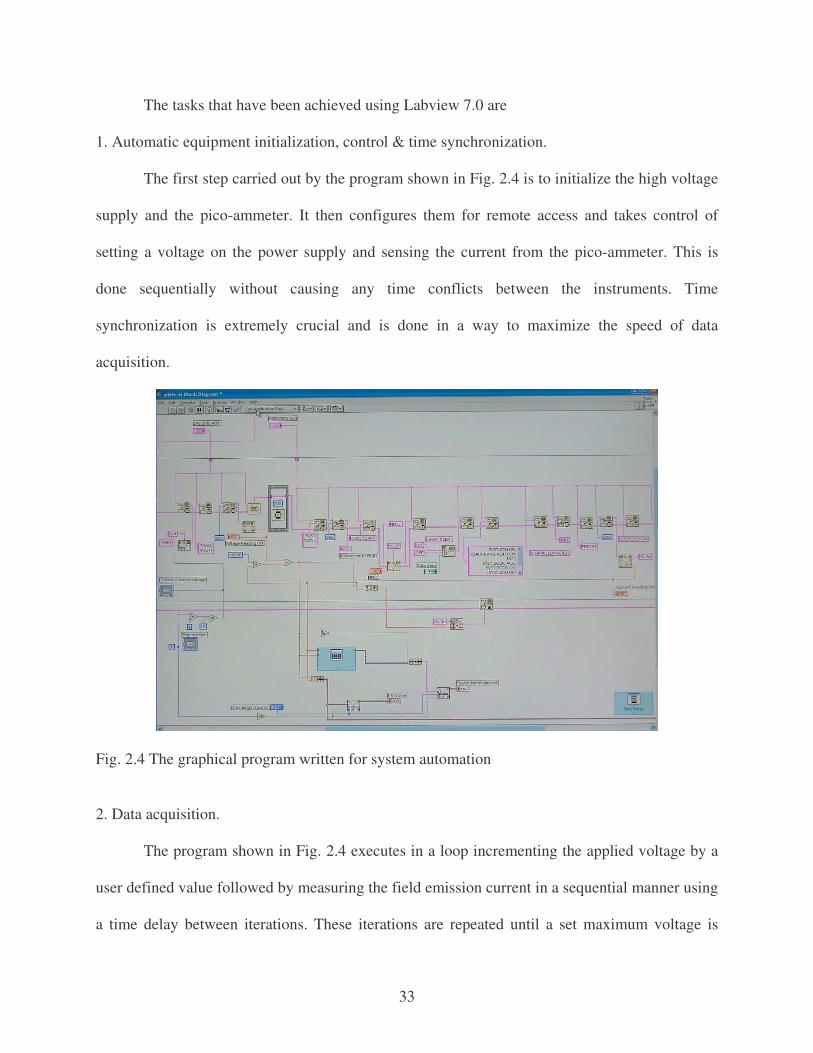
The tasks that have been achieved using Labview 7.0 are
1. Automatic equipment initialization, control & time synchronization.
The first step carried out by the program shown in Fig. 2.4 is to initialize the high voltage
supply and the pico-ammeter. It then configures them for remote access and takes control of
setting a voltage on the power supply and sensing the current from the pico-ammeter. This is
done sequentially without causing any time conflicts between the instruments. Time
synchronization is extremely crucial and is done in a way to maximize the speed of data
acquisition.
Fig. 2.4 The graphical program written for system automation
2. Data acquisition.
The program shown in Fig. 2.4 executes in a loop incrementing the applied voltage by a
user defined value followed by measuring the field emission current in a sequential manner using
a time delay between iterations. These iterations are repeated until a set maximum voltage is
34
reached. The data obtained in each iteration is written onto a data file in pairs of voltage and
current which can be used later.
3. Generation of dynamic run-time plots.
In case the CNT field emitter sample inside the chamber is destroyed and both the
electrodes get shorted in the middle of the experiment the system would continue to acquire data.
It would result in loss of time if there was no direct way of knowing about such an event. Hence
it became important to know the nature of the data getting generated as the experiment
progresses. It was also important to know if the data generated was following the Fowler-
Nordheim equation.
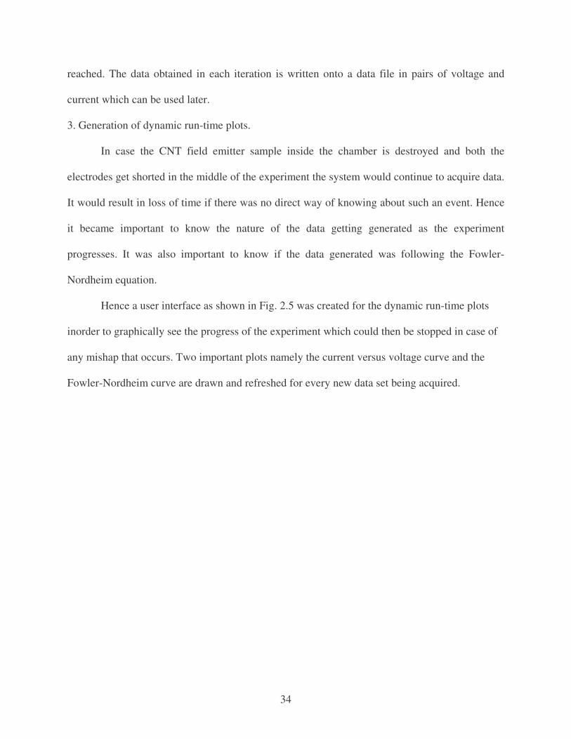
Hence a user interface as shown in Fig. 2.5 was created for the dynamic run-time plots
inorder to graphically see the progress of the experiment which could then be stopped in case of
any mishap that occurs. Two important plots namely the current versus voltage curve and the
Fowler-Nordheim curve are drawn and refreshed for every new data set being acquired.
35
Fig. 2.5 Labview User Interface showing the plot of current )(I versus Voltage )(V and also the Fowler-Nordheim plot drawn for )/ln( 2VI versus )/1( V . 4. Data Analysis
The generation of Fowler-Nordheim plot involves run-time data analysis. Labview 7.0
enables the use of mathematical functions. It allows calling and execution of Matlab (.m) files.
However the program slowed down drastically when extensive Matlab code is executed from
within Labview. Alternative approach of using mathematical functions in built in Labview is
recommended for simple data analysis. It is a recommended that a separate virtual instrument
components are written for individual steps so that the speed of the overall process is enhanced.
2.5 Advantages of the Field Emission Experimental System Designed
The advantage of the system that is designed for field emission experiments is the ease
with which one could alter any of the following parameters.
36
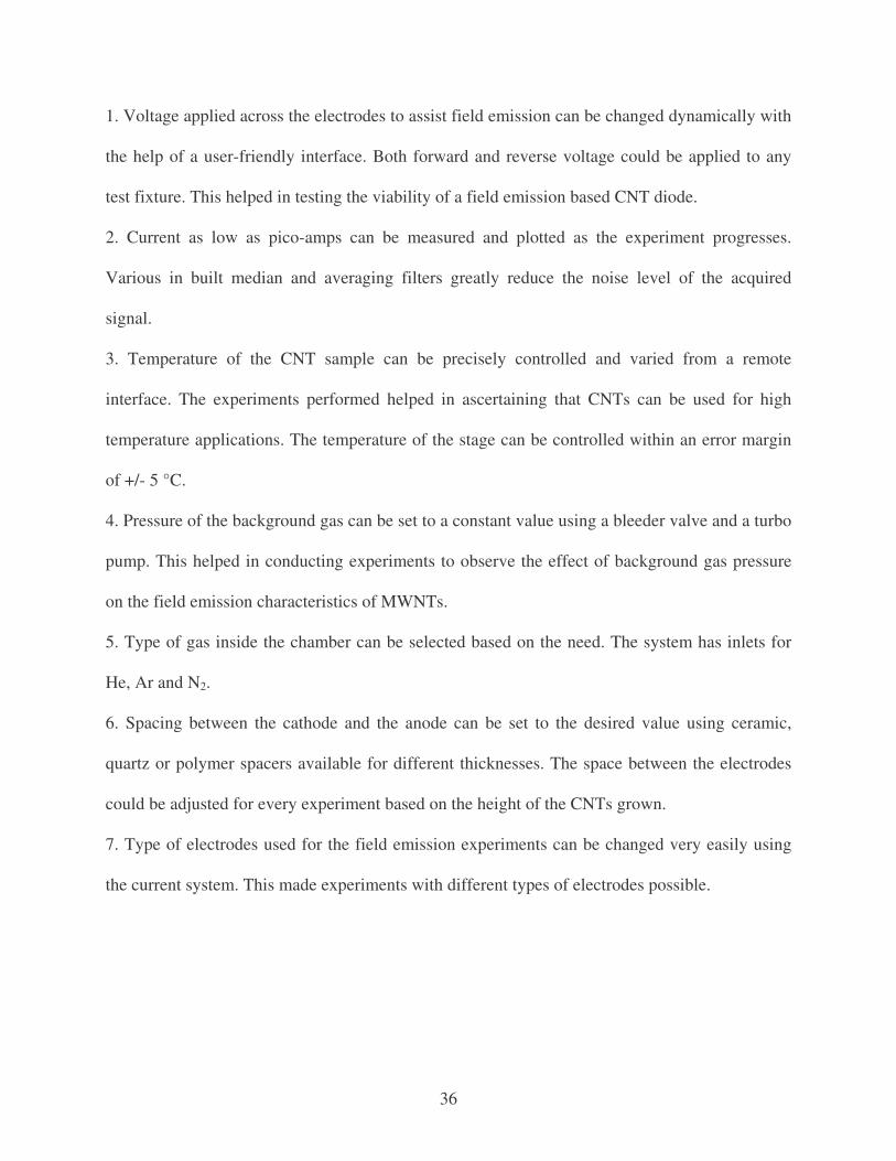
1. Voltage applied across the electrodes to assist field emission can be changed dynamically with
the help of a user-friendly interface. Both forward and reverse voltage could be applied to any
test fixture. This helped in testing the viability of a field emission based CNT diode.
2. Current as low as pico-amps can be measured and plotted as the experiment progresses.
Various in built median and averaging filters greatly reduce the noise level of the acquired
signal.
3. Temperature of the CNT sample can be precisely controlled and varied from a remote
interface. The experiments performed helped in ascertaining that CNTs can be used for high
temperature applications. The temperature of the stage can be controlled within an error margin
of +/- 5 °C.
4. Pressure of the background gas can be set to a constant value using a bleeder valve and a turbo
pump. This helped in conducting experiments to observe the effect of background gas pressure
on the field emission characteristics of MWNTs.
5. Type of gas inside the chamber can be selected based on the need. The system has inlets for
He, Ar and N2.
6. Spacing between the cathode and the anode can be set to the desired value using ceramic,
quartz or polymer spacers available for different thicknesses. The space between the electrodes
could be adjusted for every experiment based on the height of the CNTs grown.
7. Type of electrodes used for the field emission experiments can be changed very easily using
the current system. This made experiments with different types of electrodes possible.

37
3. MWNT SYNTHESIS & CHARACTERIZATION
3.1 Microfabrication
3.1.1 Lithography
CNTs selectively grow on SiO2 surface in a thermal CVD furnace. This is due to the fact
that the air-borne catalyst would react with any other surface like Au or Si forming a compound
that does not favor the growth of CNTs. The catalyst is left intact on SiO2 surface hence enabling
it to start CNT growth [25].
Hence, SiO2 was patterned to grow CNTs in different physical layouts. The CNTs grew
only on the SiO2 as expected. The CNTs thus grown in different physical layouts were tested for
field emission to study the dependence of the emitted current density on the layout. The two
parameters that were varied is pictorially shown in Fig. 3.1
Fig. 3.1 A single block of CNT islands showing the two variable parameters island size and inter-island space.
Size of the island
Space between islands
A single pattern of carbon nanotubes
38
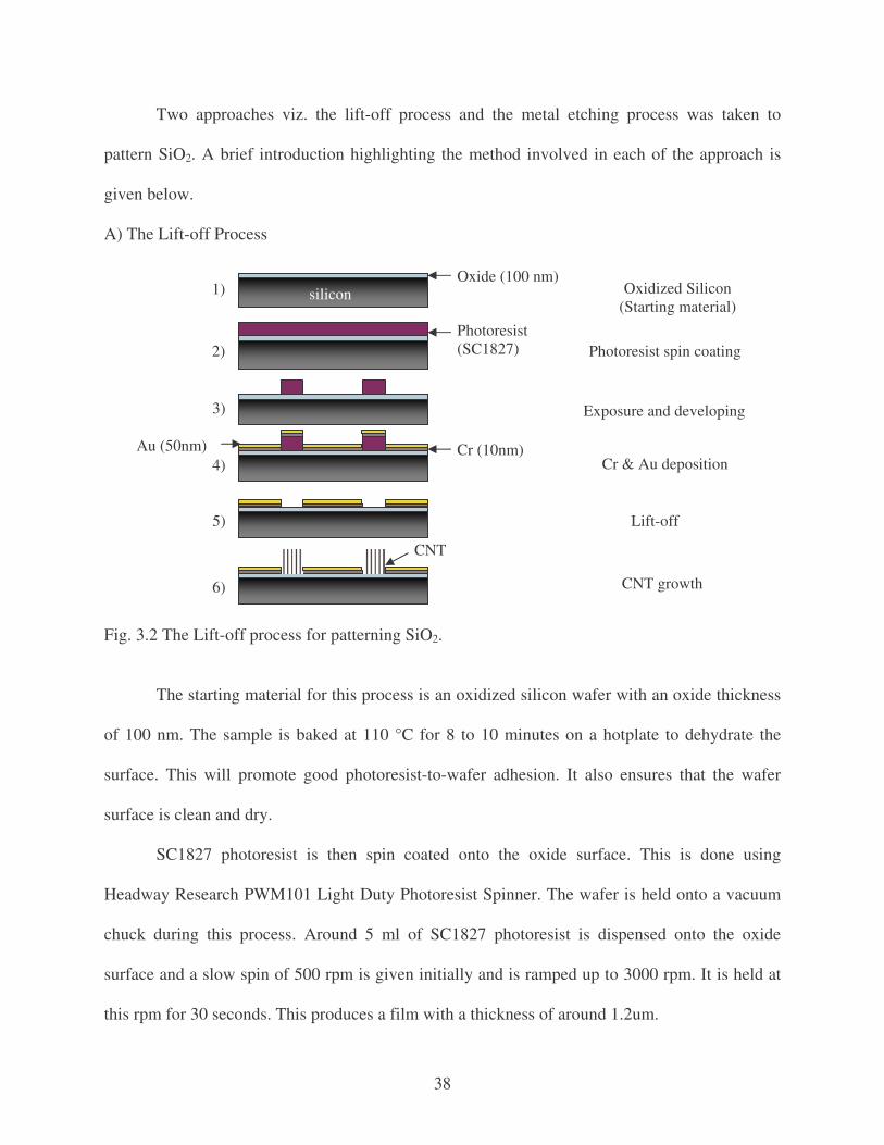
Two approaches viz. the lift-off process and the metal etching process was taken to
pattern SiO2. A brief introduction highlighting the method involved in each of the approach is
given below.
A) The Lift-off Process
Fig. 3.2 The Lift-off process for patterning SiO2.
The starting material for this process is an oxidized silicon wafer with an oxide thickness
of 100 nm. The sample is baked at 110 °C for 8 to 10 minutes on a hotplate to dehydrate the
surface. This will promote good photoresist-to-wafer adhesion. It also ensures that the wafer
surface is clean and dry.
SC1827 photoresist is then spin coated onto the oxide surface. This is done using
Headway Research PWM101 Light Duty Photoresist Spinner. The wafer is held onto a vacuum
chuck during this process. Around 5 ml of SC1827 photoresist is dispensed onto the oxide
surface and a slow spin of 500 rpm is given initially and is ramped up to 3000 rpm. It is held at
this rpm for 30 seconds. This produces a film with a thickness of around 1.2um.
1)
4)
3)
2)
Oxidized Silicon (Starting material)
silicon Oxide (100 nm)
Photoresist (SC1827)
Cr (10nm)
CNT
Photoresist spin coating
Exposure and developing
Cr & Au deposition
Lift-off
CNT growth 6)
5)
Au (50nm)
39
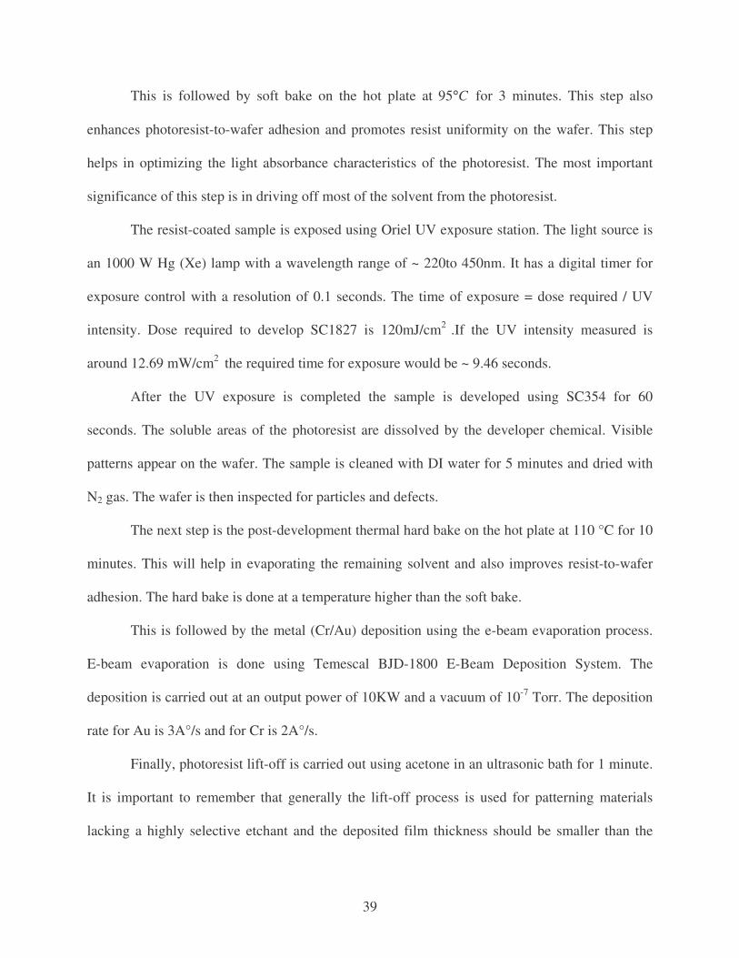
This is followed by soft bake on the hot plate at C°95 for 3 minutes. This step also
enhances photoresist-to-wafer adhesion and promotes resist uniformity on the wafer. This step
helps in optimizing the light absorbance characteristics of the photoresist. The most important
significance of this step is in driving off most of the solvent from the photoresist.
The resist-coated sample is exposed using Oriel UV exposure station. The light source is
an 1000 W Hg (Xe) lamp with a wavelength range of ~ 220to 450nm. It has a digital timer for
exposure control with a resolution of 0.1 seconds. The time of exposure = dose required / UV
intensity. Dose required to develop SC1827 is 120mJ/cm2 .If the UV intensity measured is
around 12.69 mW/cm2 the required time for exposure would be ~ 9.46 seconds.
After the UV exposure is completed the sample is developed using SC354 for 60
seconds. The soluble areas of the photoresist are dissolved by the developer chemical. Visible
patterns appear on the wafer. The sample is cleaned with DI water for 5 minutes and dried with
N2 gas. The wafer is then inspected for particles and defects.
The next step is the post-development thermal hard bake on the hot plate at 110 °C for 10
minutes. This will help in evaporating the remaining solvent and also improves resist-to-wafer
adhesion. The hard bake is done at a temperature higher than the soft bake.
This is followed by the metal (Cr/Au) deposition using the e-beam evaporation process.
E-beam evaporation is done using Temescal BJD-1800 E-Beam Deposition System. The
deposition is carried out at an output power of 10KW and a vacuum of 10-7 Torr. The deposition
rate for Au is 3A°/s and for Cr is 2A°/s.
Finally, photoresist lift-off is carried out using acetone in an ultrasonic bath for 1 minute.
It is important to remember that generally the lift-off process is used for patterning materials
lacking a highly selective etchant and the deposited film thickness should be smaller than the
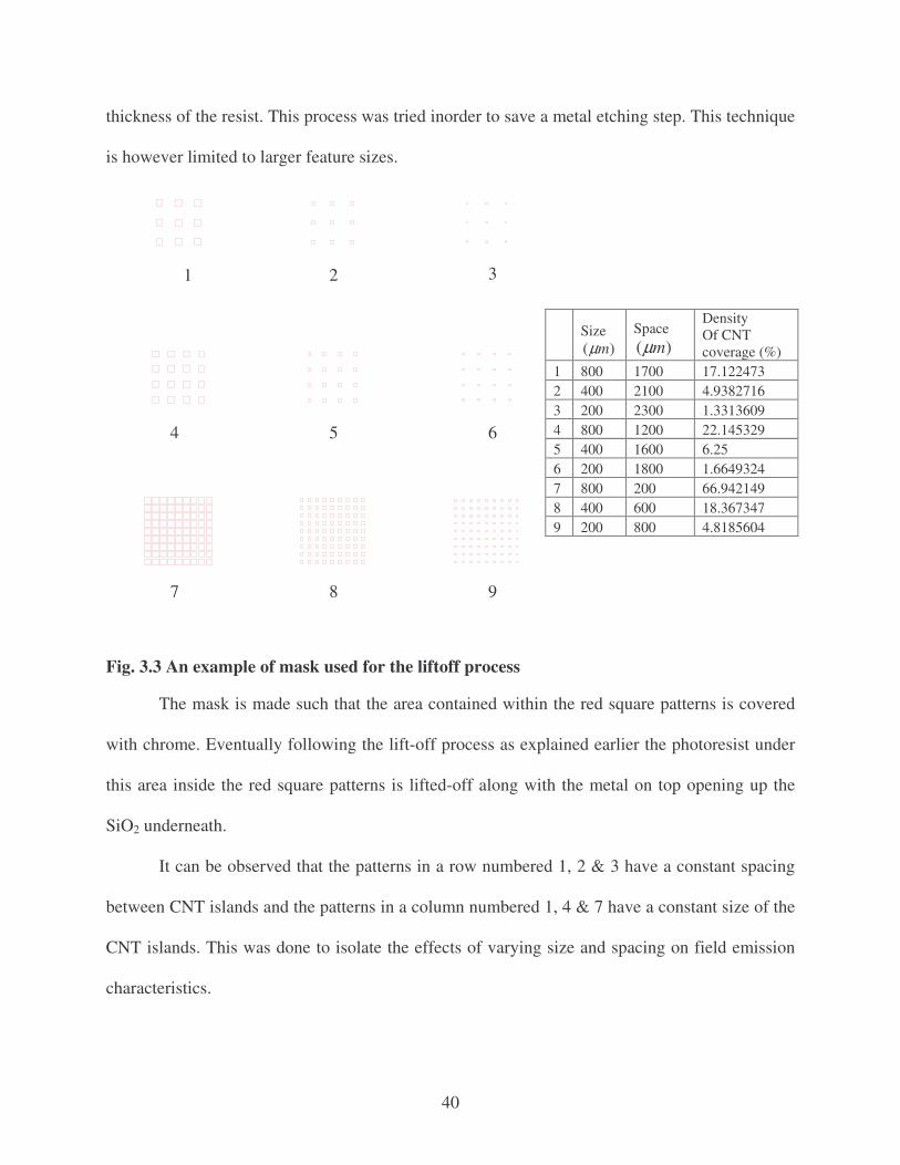
40
thickness of the resist. This process was tried inorder to save a metal etching step. This technique
is however limited to larger feature sizes.
Size
)( mµ Space
)( mµ
Density Of CNT coverage (%)
1 800 1700 17.122473 2 400 2100 4.9382716 3 200 2300 1.3313609 4 800 1200 22.145329 5 400 1600 6.25 6 200 1800 1.6649324 7 800 200 66.942149 8 400 600 18.367347 9 200 800 4.8185604
Fig. 3.3 An example of mask used for the liftoff process
The mask is made such that the area contained within the red square patterns is covered
with chrome. Eventually following the lift-off process as explained earlier the photoresist under
this area inside the red square patterns is lifted-off along with the metal on top opening up the
SiO2 underneath.
It can be observed that the patterns in a row numbered 1, 2 & 3 have a constant spacing
between CNT islands and the patterns in a column numbered 1, 4 & 7 have a constant size of the
CNT islands. This was done to isolate the effects of varying size and spacing on field emission
characteristics.
1 2 3
4 5 6
7 8 9
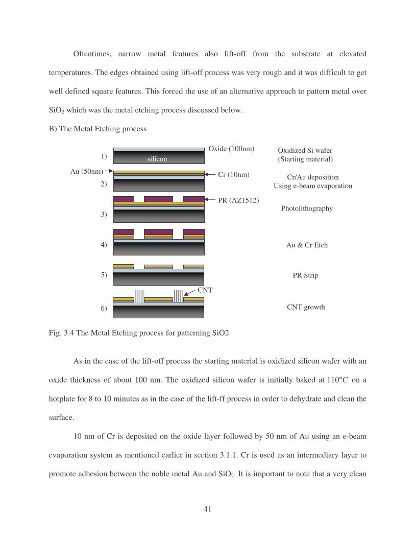
41
Oftentimes, narrow metal features also lift-off from the substrate at elevated
temperatures. The edges obtained using lift-off process was very rough and it was difficult to get
well defined square features. This forced the use of an alternative approach to pattern metal over
SiO2 which was the metal etching process discussed below.
B) The Metal Etching process
Fig. 3.4 The Metal Etching process for patterning SiO2
As in the case of the lift-off process the starting material is oxidized silicon wafer with an
oxide thickness of about 100 nm. The oxidized silicon wafer is initially baked at C°110 on a
hotplate for 8 to 10 minutes as in the case of the lift-ff process in order to dehydrate and clean the
surface.
10 nm of Cr is deposited on the oxide layer followed by 50 nm of Au using an e-beam
evaporation system as mentioned earlier in section 3.1.1. Cr is used as an intermediary layer to
promote adhesion between the noble metal Au and SiO2. It is important to note that a very clean
1)
4)
3)
2)
Oxidized Si wafer (Starting material)
Oxide (100nm)
Cr (10nm)
CNT
Photolithography
Cr/Au deposition Using e-beam evaporation
PR Strip
CNT growth 6)
5)
silicon
Au (50nm)
PR (AZ1512)
Au & Cr Etch

42
surface should be prepared before metal deposition to avoid pin holes which may result in
unwanted growth of CNT in that area causing erroneous results.
SC1827 is spin coated at 3000 rpm for 30 seconds. This resulted in a uniform layer of
resist with a thickness of around µ2.1 . Care is taken to ensure that the metal deposition is
uniform and devoid of any particles or other irregularities.
The spin coated resist is exposed using an UV exposure station. The exposed resist is
developed to obtain the desired windows in the resist layer. Inspection is carried to make sure
that the edges of the windows in the resist are sharp. If there is some resist left over the
development is carried out again under the same conditions.
After the photoresist development is complete the metals Au & Cr are etched in that
order using respective chemical etchants. The sample is inspected again to ensure the quality of
windows opened in the metal.
The remaining photoresist is stripped using acetone in an ultrasonic bath for 1 minute.
The sample is then used in the thermal CVD furnace for selective CNT growth on the SiO2.
3.1.2 Mask Preparation
The mask was designed as per the requirement for the physical layout using AutoCAD
2004. For the same pattern the mask designed for the liftoff process was complementary to that
designed for the metal etching process. During the design of the mask it is very important to
make sure that there are no open figures which will result is faulty pattern generation.
The AutoCAD file generated was converted to an ASCII format to suit the pattern
generator used to print the mask.
The mask is then printed using GCA Mann 3600 pattern generator. The minimum feature
size restriction for the pattern generator is µ4 and the positioning accuracy is µ1.0 .

43
The photoresist AZ1514 on the mask is developed after the exposure is complete. This is
followed by rinsing with DI water and drying with N2 gas. After the photoresist has been
developed, chrome etching is carried out. This is followed by cleaning again using DI water and
drying with N2 gas. Finally the remaining photoresist is stripped and the mask is cleaned. It is
important to note that these processes take very short time (1-5 minutes) hence care must be
taken to avoid over-exposure to chemical etchants.
3.2 CNT Synthesis – Thermal Chemical Vapor Deposition
Thermal chemical vapor deposition (TCVD) synthesis is achieved by putting a carbon
source in the gas phase and using an energy source, such as a resistively heated coil, to transfer
energy to a gaseous carbon containing molecule. The gaseous carbon source used was xylene.
The energy source is used to "crack" the xylene molecule into reactive atomic carbon. Then, the
carbon diffuses towards the substrate which is heated. The catalyst (usually a first row transition
metal such as Ni, Fe or Co) which initiates the CNT growth is supplied in the gas phase as
ferrocene. The ferrocene molecule breaks as a result of the thermal energy provided and the
catalyst is deposited on the substrate. The catalyst does not react with SiO2 and hence is left
intact on the oxide layer whereas it reacts with Au or Si forming a compound that does not
support CNT growth. The reactive carbon that diffuses towards the hot substrate binds with the
catalyst over the oxide layer. CNTs will be formed if the proper parameters are maintained.
Excellent alignment [26], as well as positional control on nanometer scale [27], can be achieved
by using CVD. Control over the diameter, as well as the growth rate of the nanotubes can also be
maintained. The appropriate metal catalyst can preferentially grow single rather than multi-
walled CNTs.
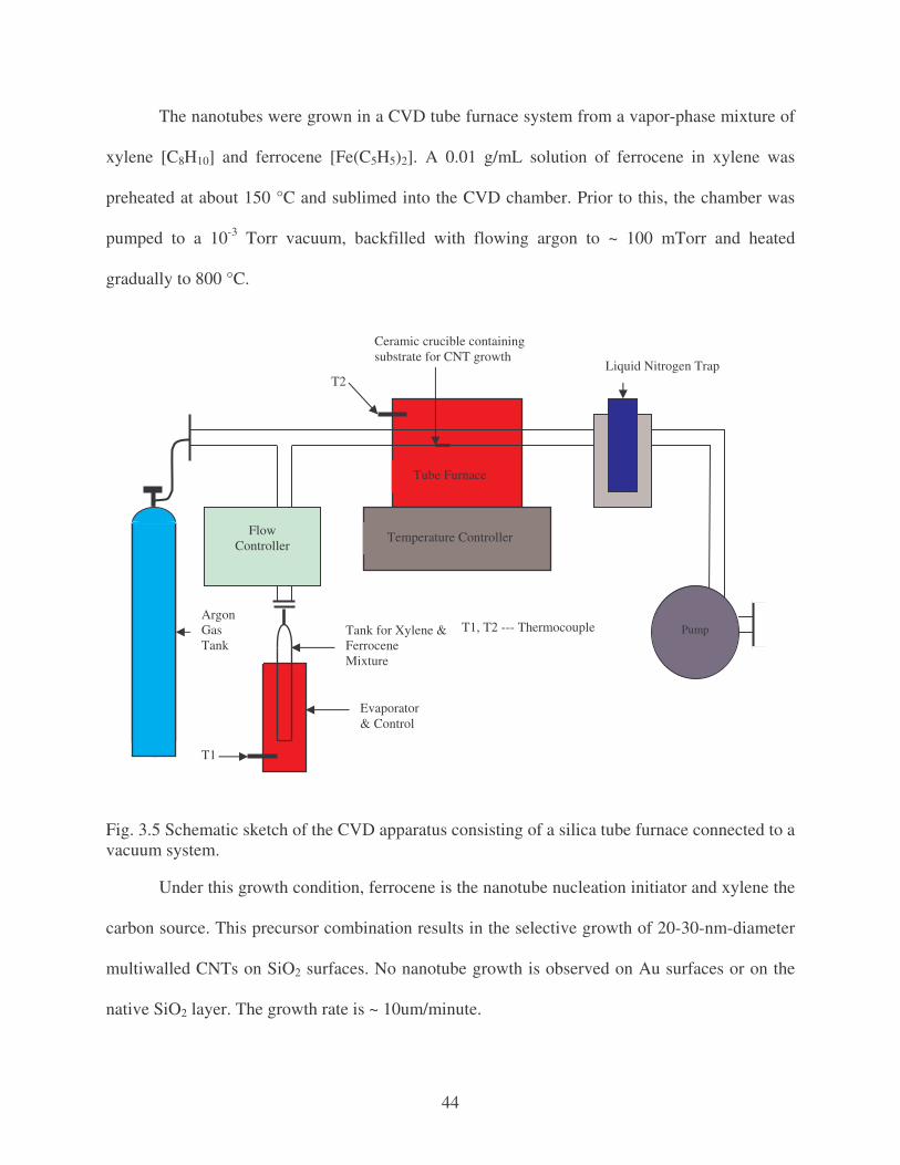
44
The nanotubes were grown in a CVD tube furnace system from a vapor-phase mixture of
xylene [C8H10] and ferrocene [Fe(C5H5)2]. A 0.01 g/mL solution of ferrocene in xylene was
preheated at about 150 °C and sublimed into the CVD chamber. Prior to this, the chamber was
pumped to a 10-3 Torr vacuum, backfilled with flowing argon to ~ 100 mTorr and heated
gradually to 800 °C.
Fig. 3.5 Schematic sketch of the CVD apparatus consisting of a silica tube furnace connected to a vacuum system.
Under this growth condition, ferrocene is the nanotube nucleation initiator and xylene the
carbon source. This precursor combination results in the selective growth of 20-30-nm-diameter
multiwalled CNTs on SiO2 surfaces. No nanotube growth is observed on Au surfaces or on the
native SiO2 layer. The growth rate is ~ 10um/minute.
Temperature Controller
Tube Furnace
Pump
Flow Controller
Evaporator & Control
Argon Gas Tank
Tank for Xylene & Ferrocene Mixture
Ceramic crucible containing substrate for CNT growth
Liquid Nitrogen Trap
T1
T2
T1, T2 --- Thermocouple

45
3.3 Electron Microscopy of CNTs Grown
A) Scanning electron microscopy (SEM): SEM measurements were carried out in a
Hitachi S-4500II Field Emission SEM equipped with a field emission gun operated at 20 keV.
Fig. 3.6(a) shows CNT grown on square islands of SiO2 patterned by opening windows in
Cr/Au.The sharp edges achieved can be seen from the Fig. 3.6(b). The Fig. 3.6(c) shows
vertically aligned Carbon Nanotubes with a length of around 60um.
(a)
(b)
(c)
Fig. 3.6 (a) Islands of CNT grown over patterned SiO2. (b) A single island of carbon nanotube. (c) Cross-sectional view of the CNT grown.
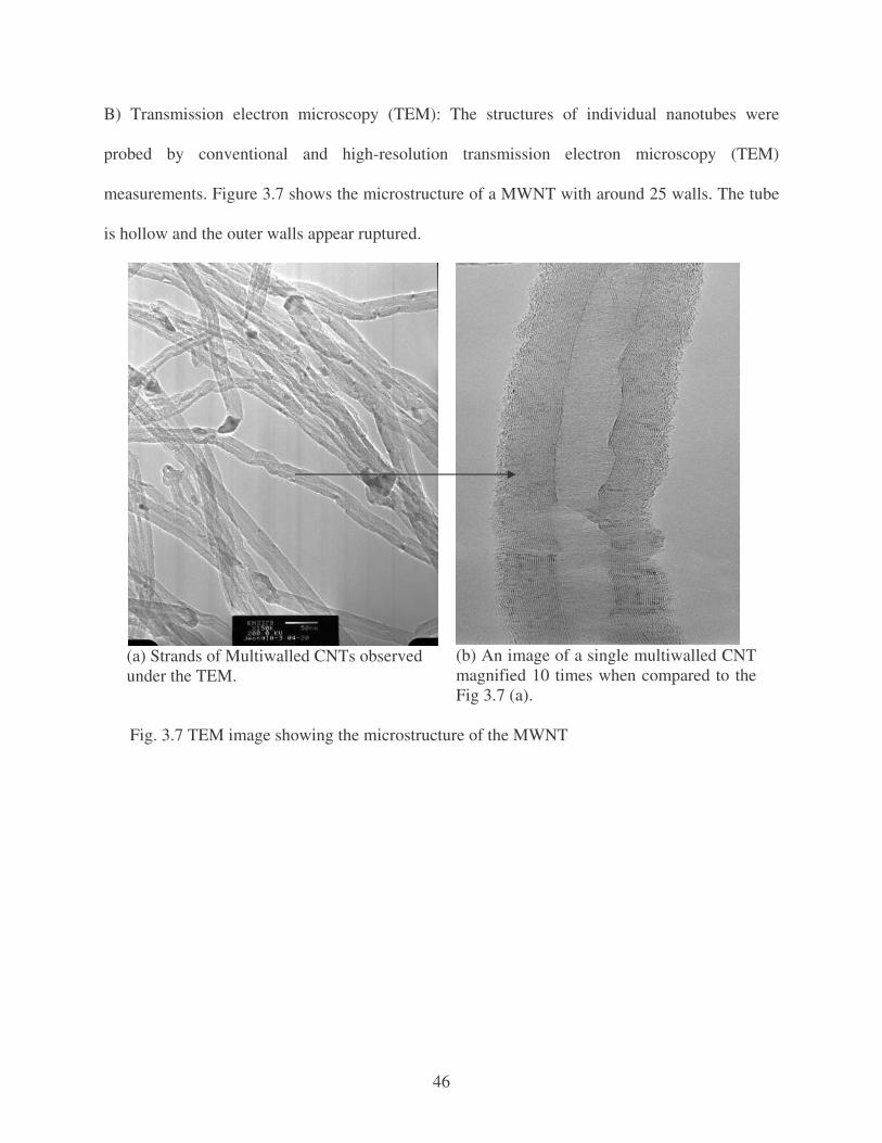
46
B) Transmission electron microscopy (TEM): The structures of individual nanotubes were
probed by conventional and high-resolution transmission electron microscopy (TEM)
measurements. Figure 3.7 shows the microstructure of a MWNT with around 25 walls. The tube
is hollow and the outer walls appear ruptured.
(a) Strands of Multiwalled CNTs observed under the TEM.
(b) An image of a single multiwalled CNT magnified 10 times when compared to the Fig 3.7 (a).
Fig. 3.7 TEM image showing the microstructure of the MWNT
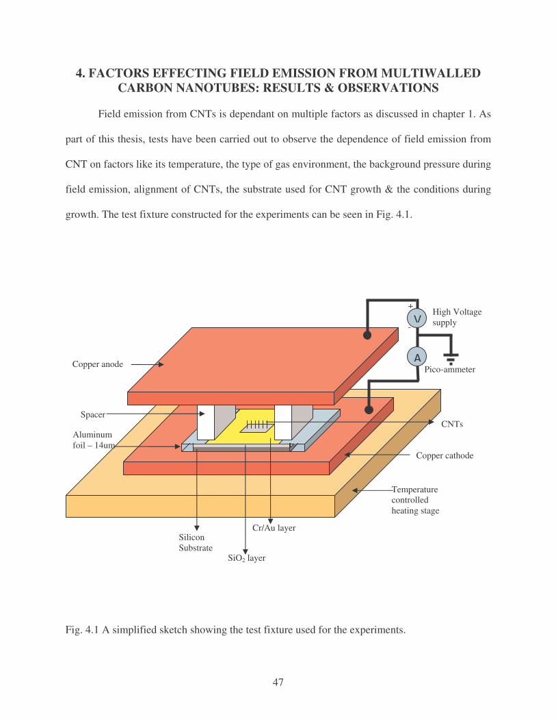
47
4. FACTORS EFFECTING FIELD EMISSION FROM MULTIWALLED CARBON NANOTUBES: RESULTS & OBSERVATIONS
Field emission from CNTs is dependant on multiple factors as discussed in chapter 1. As
part of this thesis, tests have been carried out to observe the dependence of field emission from
CNT on factors like its temperature, the type of gas environment, the background pressure during
field emission, alignment of CNTs, the substrate used for CNT growth & the conditions during
growth. The test fixture constructed for the experiments can be seen in Fig. 4.1.
Fig. 4.1 A simplified sketch showing the test fixture used for the experiments.
Copper anode
High Voltage supply
SiO2 layer
V
A
Spacer
Silicon Substrate
Cr/Au layer
+
-
Aluminum foil – 14um
Temperature controlled heating stage
Copper cathode
Pico-ammeter
CNTs
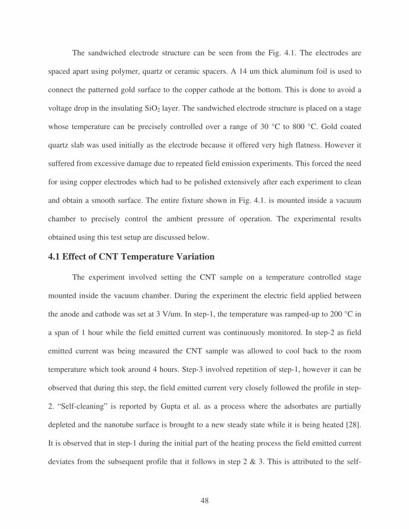
48
The sandwiched electrode structure can be seen from the Fig. 4.1. The electrodes are
spaced apart using polymer, quartz or ceramic spacers. A 14 um thick aluminum foil is used to
connect the patterned gold surface to the copper cathode at the bottom. This is done to avoid a
voltage drop in the insulating SiO2 layer. The sandwiched electrode structure is placed on a stage
whose temperature can be precisely controlled over a range of 30 °C to 800 °C. Gold coated
quartz slab was used initially as the electrode because it offered very high flatness. However it
suffered from excessive damage due to repeated field emission experiments. This forced the need
for using copper electrodes which had to be polished extensively after each experiment to clean
and obtain a smooth surface. The entire fixture shown in Fig. 4.1. is mounted inside a vacuum
chamber to precisely control the ambient pressure of operation. The experimental results
obtained using this test setup are discussed below.
4.1 Effect of CNT Temperature Variation
The experiment involved setting the CNT sample on a temperature controlled stage
mounted inside the vacuum chamber. During the experiment the electric field applied between
the anode and cathode was set at 3 V/um. In step-1, the temperature was ramped-up to 200 °C in
a span of 1 hour while the field emitted current was continuously monitored. In step-2 as field
emitted current was being measured the CNT sample was allowed to cool back to the room
temperature which took around 4 hours. Step-3 involved repetition of step-1, however it can be
observed that during this step, the field emitted current very closely followed the profile in step-
2. “Self-cleaning” is reported by Gupta et al. as a process where the adsorbates are partially
depleted and the nanotube surface is brought to a new steady state while it is being heated [28].
It is observed that in step-1 during the initial part of the heating process the field emitted current
deviates from the subsequent profile that it follows in step 2 & 3. This is attributed to the self-
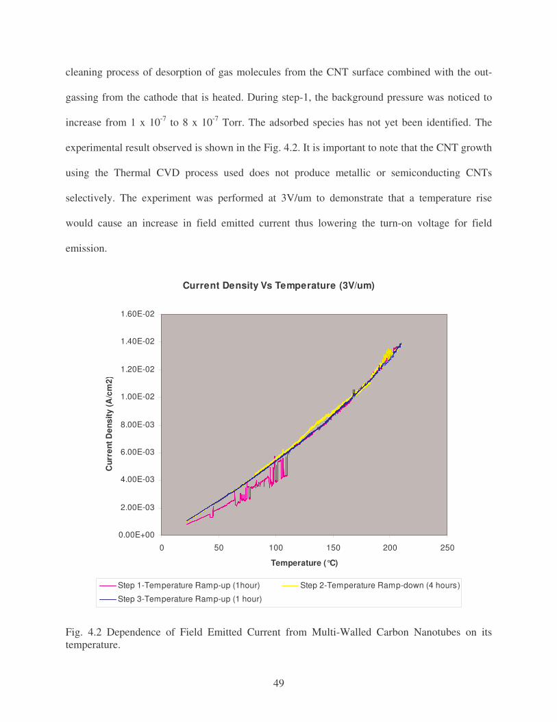
49
cleaning process of desorption of gas molecules from the CNT surface combined with the out-
gassing from the cathode that is heated. During step-1, the background pressure was noticed to
increase from 1 x 10⁻⁷ to 8 x 10⁻⁷ Torr. The adsorbed species has not yet been identified. The
experimental result observed is shown in the Fig. 4.2. It is important to note that the CNT growth
using the Thermal CVD process used does not produce metallic or semiconducting CNTs
selectively. The experiment was performed at 3V/um to demonstrate that a temperature rise
would cause an increase in field emitted current thus lowering the turn-on voltage for field
emission.
Current Density Vs Temperature (3V/um)
0.00E+00
2.00E-03
4.00E-03
6.00E-03
8.00E-03
1.00E-02
1.20E-02
1.40E-02
1.60E-02
0 50 100 150 200 250
Temperature (°C)
Cur
rent
Den
sity
(A/c
m2)
Step 1-Temperature Ramp-up (1hour) Step 2-Temperature Ramp-down (4 hours)
Step 3-Temperature Ramp-up (1 hour)
Fig. 4.2 Dependence of Field Emitted Current from Multi-Walled Carbon Nanotubes on its temperature.
50
The various possible effects of increasing CNT temperature are discussed below.
1. The observed increase in the field emitted current as a consequence of increasing the
temperature of the CNT sample could be a result of an overall decrease in the effective work
function of the CNT emitter. The change in work function could be due to one of the following
possible reasons.
a) Thermal expansion causing structural changes could result in a change in CNT work
function [29].
b) Desorption of gas molecules from the surface could alter the work function of the CNT
[30,31].
c) A possible chemical reaction at the surface of the CNT could have an effect on its work
function [32].
d) A variation in the Fermi energy level due to thermally induced carrier generation would
cause a change in the CNT work function. If the CNT is assumed to be doped the Fermi
energy level would move towards the Intrinsic energy level with rise in temperature [33].
Fig. 4.3 Change in Fermi level with rise in temperature of a doped semiconductor [1].
51
e) There is a possibility of the CNT getting doped with the catalyst/impurities as a result of
diffusion from the substrate while it is being heated. This could also alter the CNT work
function.
2. The component of Thermionic emission in the measured current becomes prominent at high
temperatures and low electric fields. ‘Richardson- Dushman’ equation, dating from 1923,
describes the current density emitted by a heated filament, as J(T) = AT2exp(-φ/kT), the value of
φ is referred to as the ‘Richardson’ work function. It is important to note that there is an intrinsic
T-dependence of the workfunction [34]. However as the temperature in the experiments
performed was not very high this effect might not be of a great significance.
3. A difference in thermal expansion co-efficients of the substrate and CNT could induce stress
at the CNT-substrate interface. This could result in possible uprooting of the CNT at high applied
electric fields causing a decrease in the overall emitting area. This being so, an overall increase
in the current with rise in temperature is observed which forces one to believe that decrease in
emitter work-function could be the most dominating factor at higher temperatures.
4. It is believed that the temperature and high current induced self-heating decreases the contact
resistance at the CNT-substrate interface which will be very significant when the field emission
device is operated at low voltages and high currents.
The result obtained as shown in Fig. 4.2 is in agreement with the data reported by Gupta
et al [28]. It can be seen from Fig. 4.4 that the applied electric field being kept constant as the
temperature of the CNT is allowed to increase from room temperature to 500°C, the intensity of
the spot on the phosphor screen placed above the field emitter initially increases reflecting a rise
in the field emitted current however as the temperature is increased further a saturation of the
emitted current is observed.

52
Fig. 4.4 The intensity of the spots on a phosphor screen due to field emission is observed to increase with temperature. From reference [28] with permission (Appendix: C9).
Current saturation is also observed at high temperatures during the experiments
performed. This is evident from the Fig. 4.5.
Fig. 4.5 Variation of current Density with temperature showing saturation at high temperature.
It is believed that as the temperature of the CNT sample is increased gradually the
emitted current becomes large enough causing the space charge effect due to ionized gases as
Temperature Ramp-up
Temperature Ramp-down
Current Saturation (3V/um)
0
0.01
0.02
0.03
0.04
0.05
0.06
0 100 200 300 400 500 600
Temperature (C)
Cur
rent
Den
sity
(A/c
m2)

53
well as emitted electrons to become prominent. The increase in space charge in the vicinity of
the emitter results in a decrease in the Electric field near the tip which in turn causes an increase
in the width of the energy barrier which the field emitted electrons have to tunnel through, thus
causing a saturation of the emitted current [36, 37]. The current saturation observed at high
temperatures could also be a result of a decrease in the effective emitting area of CNTs as a
consequence of temperature induced damage.
4.2 Effect of Background Pressure Variation
Experiments were performed to observe the effect of increasing the background pressure
in steps of 1 order of magnitude. The multiwalled CNT sample (grown using the thermal CVD
setup discussed in section 3). was initially mounted inside the vacuum chamber and the pressure
is lowered to 1x10⁻⁶ Torrs. This is followed by flushing the chamber with N2 back to atmospheric
pressure. This cycle of evacuating and flushing is repeated several times to ensure that there is no
other gas besides N2 present inside the chamber. This is followed by sweeping the applied
voltage and measuring the field emitted current at different background pressures ranging from
1x10⁻⁶ Torr to 1x10⁻⁴ Torr. The results obtained are shown in Fig. 4.6, Fig. 4.7 and Fig. 4.8.
The various possible effects of increasing the background gas pressure are as follows.
a) Adsorption of gas molecules on the CNT surface increases with the background pressure
until a saturation is reached. This would result in a change in work function of the
emitter.
b) As the background pressure in the chamber is increased the component of gas ionization
current begins to dominate.
c) If the temperature, applied electric field, and the inter-electrode distance are kept constant
and the background pressure increased gradually, at a certain value of pressure, unique to

54
the gas being used, negatively charged plasma (CNT emitter sample is mounted on the
cathode) begins to appear causing arcs between the anode and the cathode.
d) Bombardment by positively charged ions present in the vicinity of the emitter could
result in CNT surface degradation.
e) Damage caused to the gold plated surface surrounding the CNT patterned islands
resulting in sharp edged craters might cause an increase in the background noise in the
current measured.
f) The columbic field generated by the positively charged gas ions in the vicinity of the
emitter is dominant at high background pressures. This space charge effect at high
background pressures could result in an increase in the width of the potential barrier
resulting in a decrease in the field emission current
Effect of Pressure Variation (Nitrogen)
0.00E+00
5.00E-05
1.00E-04
1.50E-04
2.00E-04
2.50E-04
3.00E-04
3.50E-04
0 500 1000 1500 2000 2500
Applied Voltage (V)
Mea
sure
d cu
rren
t (A
)
Pressure - 1.0E-6 Torrs Pressure - 1.00E-5 Torrs Pressure - 1.0E-4 Torrs
Fig. 4.6 (a)
Fig. 4.6 Effect of change in background pressure of Nitrogen on field emitted current. (fig. contd.)
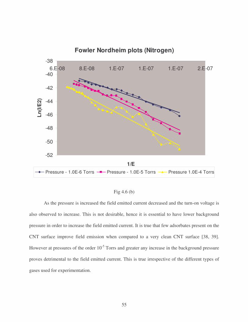
55
Fowler Nordheim plots (Nitrogen)
-52
-50
-48
-46
-44
-42
-40
-386.E-08 8.E-08 1.E-07 1.E-07 1.E-07 2.E-07
1/E
Ln(I/
E2)
Pressure - 1.0E-6 Torrs Pressure - 1.0E-5 Torrs Pressure 1.0E-4 Torrs
Fig 4.6 (b)
As the pressure is increased the field emitted current decreased and the turn-on voltage is
also observed to increase. This is not desirable, hence it is essential to have lower background
pressure in order to increase the field emitted current. It is true that few adsorbates present on the
CNT surface improve field emission when compared to a very clean CNT surface [38, 39].
However at pressures of the order 10-5 Torrs and greater any increase in the background pressure
proves detrimental to the field emitted current. This is true irrespective of the different types of
gases used for experimentation.
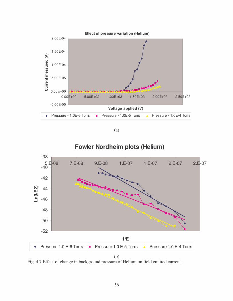
56
Effect of pressure variation (Helium)
-5.00E-05
0.00E+00
5.00E-05
1.00E-04
1.50E-04
2.00E-04
0.00E+00 5.00E+02 1.00E+03 1.50E+03 2.00E+03 2.50E+03
Voltage applied (V)
Cur
rent
mea
sure
d (A
)
Pressure - 1.0E-6 Torrs Pressure - 1.0E-5 Torrs Pressure - 1.0E-4 Torrs
(a)
Fowler Nordheim plots (Helium)
-52
-50
-48
-46
-44
-42
-40
-385.E-08 7.E-08 9.E-08 1.E-07 1.E-07 2.E-07 2.E-07
1/E
Ln(I/
E2)
Pressure 1.0 E-6 Torrs Pressure 1.0 E-5 Torrs Pressure 1.0 E-4 Torrs
(b) Fig. 4.7 Effect of change in background pressure of Helium on field emitted current.

57
Effect of Pressure Variation (Argon)
0.00E+00
2.00E-05
4.00E-05
6.00E-05
8.00E-05
1.00E-04
1.20E-04
0.00E+00 5.00E+02 1.00E+03 1.50E+03 2.00E+03 2.50E+03Voltage applied (V)
Cur
rent
Mea
sure
d (A
)
Pressure - 1.0E-6 Torrs Pressure - 1.0E-5 Torrs Pressure - 1.0E-4 Torrs
(a)
Fowler Nordheim Plots (Argon)
-55
-53
-51
-49
-47
-45
-43
-416.E-08 8.E-08 1.E-07 1.E-07 1.E-07 2.E-07 2.E-07
1/E
Ln(I/
E2)
Pressure - 1.0E-6 Torrs Pressure - 1.0E-5 Torrs Pressure -1.0E-4 Torrs
(b) Fig. 4.8 Effect of change in background pressure of Argon on field emitted current.
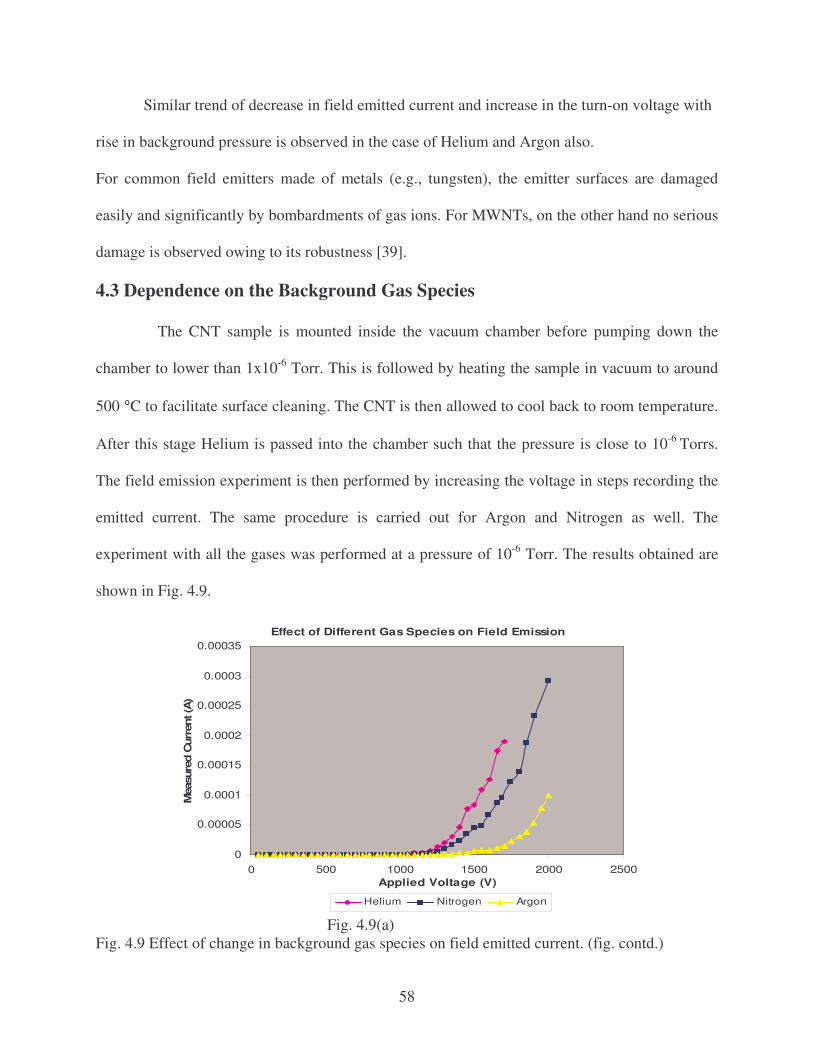
58
Similar trend of decrease in field emitted current and increase in the turn-on voltage with
rise in background pressure is observed in the case of Helium and Argon also.
For common field emitters made of metals (e.g., tungsten), the emitter surfaces are damaged
easily and significantly by bombardments of gas ions. For MWNTs, on the other hand no serious
damage is observed owing to its robustness [39].
4.3 Dependence on the Background Gas Species
The CNT sample is mounted inside the vacuum chamber before pumping down the
chamber to lower than 1x10⁻⁶ Torr. This is followed by heating the sample in vacuum to around
500 °C to facilitate surface cleaning. The CNT is then allowed to cool back to room temperature.
After this stage Helium is passed into the chamber such that the pressure is close to 10-6 Torrs.
The field emission experiment is then performed by increasing the voltage in steps recording the
emitted current. The same procedure is carried out for Argon and Nitrogen as well. The
experiment with all the gases was performed at a pressure of 10-6 Torr. The results obtained are
shown in Fig. 4.9.
Effect of Different Gas Species on Field Emission
0
0.00005
0.0001
0.00015
0.0002
0.00025
0.0003
0.00035
0 500 1000 1500 2000 2500Applied Voltage (V)
Mea
sure
d C
urre
nt (A
)
Helium Nitrogen Argon
Fig. 4.9(a) Fig. 4.9 Effect of change in background gas species on field emitted current. (fig. contd.)

59
Fowler Nordheim Plots
-54
-52
-50
-48
-46
-44
-42
-40
-387.E-08 9.E-08 1.E-07 1.E-07 2.E-07 2.E-07 2.E-07 2.E-07
1/E
Ln(I/
E2)
Helium Nitrogen Argon
Fig. 4.9 (b) Different gases interact with the CNT surface in a different way which is the reason for
the observed variation in the field emitted current as the background gas species is changed. The
field emitted current depends strongly on the work function and geometry of the surface, and
thus is very susceptible to gas exposures [12].
Adsorption of molecules causes a charge transfer and is believed to determine the
direction of the dipole field at the CNT edges. It is assumed that the adsorbed gas species causes
a shift in the Fermi level (a change in the work function) which in turn changes the available
density of states near the Fermi level [38]. This would directly influence the field emitted
current. However the different interaction mechanism for individual gas species is not clear..
It is believed that Nitrogen and Argon tends to degrade the emitter whereas He is
observed to cause relatively no degradation [40]. This can be inferred from the results in Fig. 4.9.
4.4 Dependence on CNT Orientation (Random Vs Aligned)
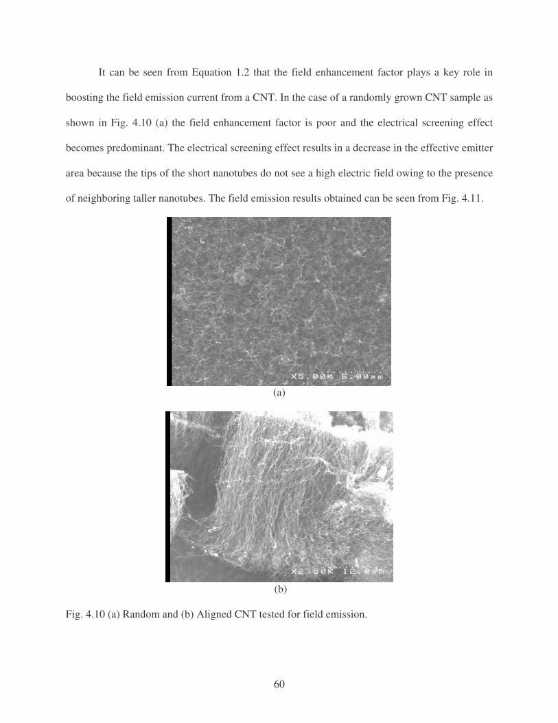
60
It can be seen from Equation 1.2 that the field enhancement factor plays a key role in
boosting the field emission current from a CNT. In the case of a randomly grown CNT sample as
shown in Fig. 4.10 (a) the field enhancement factor is poor and the electrical screening effect
becomes predominant. The electrical screening effect results in a decrease in the effective emitter
area because the tips of the short nanotubes do not see a high electric field owing to the presence
of neighboring taller nanotubes. The field emission results obtained can be seen from Fig. 4.11.
(a)
(b)
Fig. 4.10 (a) Random and (b) Aligned CNT tested for field emission.
61
Effect of Alignment on CNT Field Emission
0
5
10
15
20
25
0 500 1000 1500 2000Applied Voltage (V)
Mea
sure
d C
urre
nt D
ensi
ty (A
/cm
2)
Aligned Random
(a)
Fowler Nordheim plots
-50-45-40-35-30-25-20-15-10-50
0.E+00 2.E-07 4.E-07 6.E-07 8.E-07 1.E-06 1.E-06 1.E-06
1/E
Ln(I/
E2)
Aligned Random
(b) Fig. 4.11 Effect of CNT alignment on field emitted current.
It can be seen from the data obtained that an alignment in the CNT grown greatly
enhances the field emission characteristic. It has also been observed that even though the random
CNTs have poor field emission characteristics they tend to offer better life time [8]. This could
62
be due to the way they are oriented giving better mechanical strength to bear the electrostatic
force acting on them during field emission.
4.5 Effect of the Substrate Material Used for Growth
The substrate material has a substantial influence on the field emitted current density as
well as on the turn-on electric field as observed in fig 4.12. It is evident that metallic substrates
are superior to non-metallic ones.
There are various ways in which an underlying substrate can influence field emission.
1. The type and structure of CNT grown depends on the substrate used [20]. This has been
observed during characterization done on the CNTs.
2. The strength with which the CNT holds on to the base material depends on the type of
substrate. During CNT growth, an amorphous substrate like SiO2 could give a better
physical adhesion to the CNT grown than a crystalline metallic substrate like Nickel. This
could control the lifetime of a CNT emitter.
3. The electrical conduction mechanism within the substrate material under different
conditions of operation (viz. temperature, voltage) varies depending on its type.
4. The breakdown mechanism at high temperature or applied electric field depends on the
type of substrate used. Metallic substrates tend to suffer from thermal runaway at high
current densities and elevated temperatures of operation.
5. The background field emission which accounts for the noise in the measured current
depends on the morphology of the substrate employed. A highly smooth substrate surface
is ideal for use.
6. The contact resistance depends on the nature of the CNT-substrate interface.

63
Effect of Substrates on CNT Field Emission
0.00E+00
1.00E-03
2.00E-03
3.00E-03
4.00E-03
5.00E-03
6.00E-03
0 2 4 6 8 10 12 14Applied Electric field (V/um)
Mea
sure
d C
urre
nt D
ensi
ty (A
/cm
2)
Stainless Steel Nickel Silicon dioxide Vanadium Oxide
(a)
(b)
Fig. 4. 12 Effect of the type of substrate on field emitted current.

64
4.6 Other Experimental Observations
4.6.1 CNT Emitter Degradation
It is observed that the CNT field emitter suffers a gradual degradation as a result of
multiple rounds of field emission experiments. The islands of patterned CNT emitters tend to
leave an imprint on the anode surface. As a result of emitter degradation some of the imprints
disappear after subsequent rounds of field emission experiments. This can be observed in
Fig.4.13. The image has a magnification of 5
(a) First experiment (b) Second Experiment
(c) Third experiment
Fig. 4.13 Few of the imprints on the anode surface disappear after each experiment owing to CNT degradation.
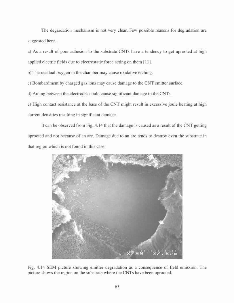
65
The degradation mechanism is not very clear. Few possible reasons for degradation are
suggested here.
a) As a result of poor adhesion to the substrate CNTs have a tendency to get uprooted at high
applied electric fields due to electrostatic force acting on them [11].
b) The residual oxygen in the chamber may cause oxidative etching.
c) Bombardment by charged gas ions may cause damage to the CNT emitter surface.
d) Arcing between the electrodes could cause significant damage to the CNTs.
e) High contact resistance at the base of the CNT might result in excessive joule heating at high
current densities resulting in significant damage.
It can be observed from Fig. 4.14 that the damage is caused as a result of the CNT getting
uprooted and not because of an arc. Damage due to an arc tends to destroy even the substrate in
that region which is not found in this case.
Fig. 4.14 SEM picture showing emitter degradation as a consequence of field emission. The picture shows the region on the substrate where the CNTs have been uprooted.
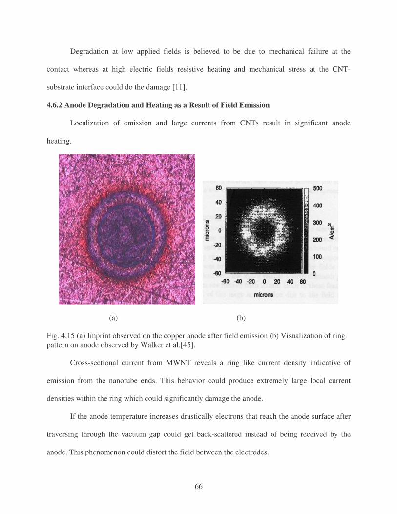
66
Degradation at low applied fields is believed to be due to mechanical failure at the
contact whereas at high electric fields resistive heating and mechanical stress at the CNT-
substrate interface could do the damage [11].
4.6.2 Anode Degradation and Heating as a Result of Field Emission
Localization of emission and large currents from CNTs result in significant anode
heating.
(a) (b)
Fig. 4.15 (a) Imprint observed on the copper anode after field emission (b) Visualization of ring pattern on anode observed by Walker et al.[45]. Cross-sectional current from MWNT reveals a ring like current density indicative of
emission from the nanotube ends. This behavior could produce extremely large local current
densities within the ring which could significantly damage the anode.
If the anode temperature increases drastically electrons that reach the anode surface after
traversing through the vacuum gap could get back-scattered instead of being received by the
anode. This phenomenon could distort the field between the electrodes.
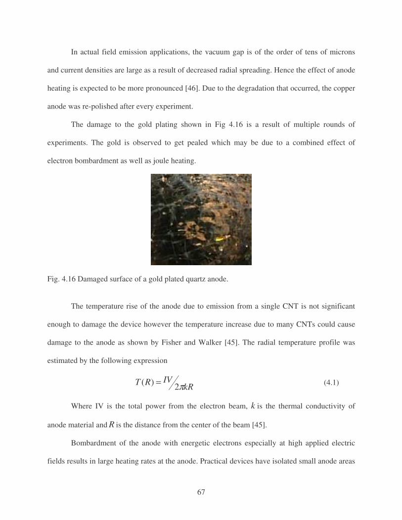
67
In actual field emission applications, the vacuum gap is of the order of tens of microns
and current densities are large as a result of decreased radial spreading. Hence the effect of anode
heating is expected to be more pronounced [46]. Due to the degradation that occurred, the copper
anode was re-polished after every experiment.
The damage to the gold plating shown in Fig 4.16 is a result of multiple rounds of
experiments. The gold is observed to get pealed which may be due to a combined effect of
electron bombardment as well as joule heating.
Fig. 4.16 Damaged surface of a gold plated quartz anode.
The temperature rise of the anode due to emission from a single CNT is not significant
enough to damage the device however the temperature increase due to many CNTs could cause
damage to the anode as shown by Fisher and Walker [45]. The radial temperature profile was
estimated by the following expression
kRIVRT π2)( = (4.1)
Where IV is the total power from the electron beam, k is the thermal conductivity of
anode material and R is the distance from the center of the beam [45].
Bombardment of the anode with energetic electrons especially at high applied electric
fields results in large heating rates at the anode. Practical devices have isolated small anode areas

68
which could create problem of continuous heat dissipation during its operation. For devices
designed to carry large current densities, anode heating can cause erosion or catastrophic failure
of the device
4.6.3 Young’s Interference Fringes
Electron beams can be treated as waves which interfere either constructively or
destructively depending on the phase shift caused by the different path lengths of the electrons. If
the geometrical configuration of the two emission sites causes a phase shift ofπ it results in
destructive interference resulting in a dark line in the interference fringes. If the phase shift is
2π it results in constructive interference corresponding to a bright line.
Young’s interference fringes have been found after field emission experiments on the copper
anode surface as an imprint.
As reported by T. Yamashita et al., the Fig. 4.17 shows how chemisorption of molecules
on emission sites results in bright spots with young’s interference fringes in the background.
Fig. 4. 17 Typical Field emission microscope (FEM) image of a MWNT during field emission. From reference [47] with permission (Appendix: C10).

69
Bright spots as well as the interference fringes were observed after the field emission
experiment. It is known that the electron beam spreads as a result of coulomb interaction
however the initial ring is preserved [46]. The concentric nature of the interference fringes (fig
4.18) verifies the flatness of the anode with respect to the emitter.
(a) (b) Fig. 4. 18 Young’s interference fringes found on the anode surface
Temperature was observed to have a significant effect in increasing the field emitted
current from multiwalled CNTs. Deterioration in field emission characteristics with increase in
the ambient pressure of operation was noticed. Dependence of field emission from multiwalled
CNTs on the type of surrounding gas was established. The relation between the alignment of the
MWNTs grown and their field emission characteristics was studied. Different types of substrates
were used for CNT growth and the various ways it affects the field emission properties were
analyzed. Other experimental observations like CNT emitter damage, anode heating and
formation of young’s interference fringes have been reported.
70
5. CONCLUSION AND SUGGESTIONS FOR FUTURE RESEARCH 5.1 Summary and Conclusions
Discussion of the basic physics that governs field emission including the different aspects
of the Fowler Nordheim Model has been given in chapter 1. Different factors that affect field
emission from MWNTs have been discussed. Different parameters that can be controlled in order
to optimize field emission are highlighted and analytical expressions showing how these
variables influence the net field emitted current are mentioned. Some of the existing works on
similar topics in the literature are visited and their important results are magnified. Detailed
analysis of the experimental requirements was carried out. System to study the effect of various
factors on field emission from MWNTs was designed and assembled. The main features and
advantages of the system have been discussed in chapter 2. Results of the field emission
experiments performed and various observations made have been discussed in chapter 4.
Experimental results have been explained with analytical discussions wherever possible. The
main goal of the experiments performed was to identify the relation between field emission from
MWNTs and the various factors that influenced it. The results obtained will be useful in
choosing the conditions for operation of a field emission device.
One of the contributions of this work is that it shows how temperature affects the field
emitted current density. Contrary to the belief that field emission is relatively insensitive to
temperature changes, it has been shown that variations in temperature have a significant effect on
the field emitted current from MWNTs. One of the reasons for this may be the change in the
CNT emitter work function as a result of heating. This result shall be critical for high
temperature applications of CNT field emission based devices.

71
At relatively poor vacuum in the range of 10-6 Torrs to 10-3 Torrs it has been observed
that any increase in pressure results in deterioration of the performance of CNT field emitters.
This effect of pressure on field emission has been verified with three different types of gases viz.
Ar, He and N2. This result could be made use of in pressure sensing applications.
It has been demonstrated that a change in the background gas species affects the field
emission from CNTs all other parameters remaining the same. Effect of CNT alignment and the
substrate used for CNT growth on the field emission characteristics have been reported. It has
been shown that conditions during growth also have an impact on the FE property.
Other important experimental observations have been made. CNT emitter degradation
and the various possible mechanisms that could cause it have been discussed. Anode surface
degradation and heating as a result of field emission has been reported. Young’s interference
rings have been observed on the anode surface as a consequence of field emission.
The results obtained as part of this work can be used to optimize the performance of a
MWNT based field emission device in terms of the field emitted current density and the required
turn-on voltage.
5.2 Prospects & Limitations
Today the most mature technology to produce gated micro field electron emitter arrays is
the so called Spindt-type metal micro-tip process. The drawbacks of the Spindt-type process are
expensive production technique, relatively poor lifetime in technical vacuum and the high
operating voltages required. CNTs can be regarded as the potential second-generation technology
to Spindt-type metal micro-tips. The use of CNTs as field enhancing structures in electron
emission sources can bring several advantages such as longer lifetime and operation in poor
vacuum due to the high chemical inertness as well as low operation voltages and perhaps most
72
important of all is its very low cost production technique. CNTs do not suffer from thermal
runaway at high temperatures (except metallic CNT). However emitter degradation at high
emission currents limits the full exploitation of high emission site density that can be achieved
using CNTs. The emission degradation becomes apparent for emission currents in the micro-
amps range for a single emitter. High power dissipation could be a cause for the damage.
Therefore, although the fundamental properties of CNTs are very favorable for the use as field
emission tips, these properties alone will not guarantee their success in this area. A perfect
control of the catalytic CNT growth process is needed for the success of CNT field emitter
technology, more so for high current applications.
5.3 Suggested Enhancements in the Experimental System
The suggested improvements to the experimental system designed are discussed below
a) A modification in the Labview program incorporating a faster data acquisition algorithm
would help in reducing the time taken for each experiment which is currently around 4 hours.
b) The contacts between the power feed-through, wires and the electrodes should be modified to
reduce the noise level. This would become crucial while making very low current measurements
(< 10 nA).
c) The size of the vacuum chamber used should be reduced to achieve higher vacuum level. A
pressure controller is required to accurately control the pressure inside the chamber. The current
method used is prone to minor fluctuations.
d) A voltage source that could supply voltage higher than 5 KV would be very beneficial.
e) Inter-electrode spacing is currently adjusted using ceramic, quartz or polymer spacers. Once
the spacing is fixed it is not possible to adjust it without breaking the vacuum in the chamber. It
would be advantageous to have a dynamically adjustable system using a linear motion feed
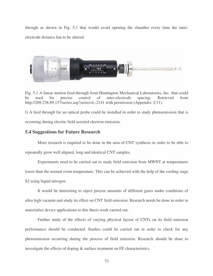
73
through as shown in Fig. 5.1 that would avoid opening the chamber every time the inter-
electrode distance has to be altered.
Fig. 5.1 A linear motion feed-through from Huntington Mechanical Laboratories, Inc.that could be used for precise control of inter-electrode spacing. Retrieved from http://209.238.89.157/series.asp?series=L-2141 with permission (Appendix: C11). f) A feed through for an optical probe could be installed in order to study photoemission that is
occurring during electric field assisted electron emission.
5.4 Suggestions for Future Research
More research is required to be done in the area of CNT synthesis in order to be able to
repeatedly grow well aligned, long and identical CNT samples.
Experiments need to be carried out to study field emission from MWNT at temperatures
lower than the normal room temperature. This can be achieved with the help of the cooling stage
S2 using liquid nitrogen.
It would be interesting to inject precise amounts of different gases under conditions of
ultra high vacuum and study its effect on CNT field emission. Research needs be done in order to
materialize device applications to this thesis work carried out.
Further study of the effects of varying physical layout of CNTs on its field emission
performance should be conducted. Studies could be carried out in order to check for any
photoemission occurring during the process of field emission. Research should be done to
investigate the effects of doping & surface treatment on FE characteristics.

74
It is also important to study how field emission depends on various device configurations
including a planar design. Simulations should be carried out to understand the influence of
various experimental and growth related factors on field emission from MWNTs. Tools written
using Matlab 7.0 for data analysis & curve fitting (Appendix B) can be used for this purpose.
75
REFERENCES
[1] Antonius Gerardus Johannes Van Oostrom, “Validity of the Fowler-Nordheim Model for Field Electron Emission”, 1965. [2] Z. Kosakovskaya and Yu. Gulayev, “Field-emission from vertically-aligned multiwalled carbon nanotube films doped by different elements”, Electronic properties of nanotubes P44, Institute of Radio engineering and Electronics of RAS, 10,1999 Moscow, Russia. [3] Robert J. Nemanich, Jim L. Davidson, Weng Poo Kang, “Electron Field Emitters Based on Carbon Materials”, ADC – FCT 2001. [4] W.W.Dolan and W.P.Dyke, “Temperature-and-Field Emission of Electrons from Metals”, Physical Review 95, 327-332, 1954. [5] Robert A. Millikan, and Charles C. Lauritsen, “Dependence of Electron Emission from Metals upon Field Strengths and Temperatures”, Physical Review 33, 598 (1929). [6] Peng Li, Kaili Jiang, Ming Liu, Qunqing Li, and Shoushan Fan, “Polarized Incandescent Light Emission from Carbon Nanotubes”, Applied Physics Letters 82, 1763, (2003). [7] Ali Javey, Pengfei Qi, Qian Wang and Hongjie Dai, “Ten to 50 nm long quasi-ballistic carbon nanotube devices obtained without complex lithography” 13408-13410, NAS, Vol.101,no.37,2004. [8] Jean-Marc Bonard, Mirko Croci, Christian Klinke, Fabien Conus, Imad Arfaoui, Thomas Stockli, and Andre Chatelain, “Growth of Carbon Nanotubes Characterized by field emission measurements during chemical vapor deposition”, Physical Review B 67, 085412 (2003). [9] M.W. Docter, C.W. Hagen, P. Kruit, “Field emission stability of carbon nanotubes”, Proceedings of the Nederlandse Vereniging voor Microscopie 2003 meeting in Papendal, Arnhem, December 11-12, 2003, in Jaarboek 2003 NVvM, pg. 148-150. [10] Babu R. Chalamala and Robert H. Reuss, “Real-time measurement of pressure inside field-emission displays”, Applied Physics Letters, Volume 79, Number 16, 2648-2650, 2001. [11] Jean-Marc Bonard, Christian Klinke, Kenneth A. Dean and Bernard F. Coll, “Degradation and failure of carbon nanotube field emitters”, Physical review B 67, 115406, 2003. [12] A.Wadhawan, R.E.Stallcup II, K.F.Stephens II, and J.M. Perez, “Effects of O2, Ar, and H2, gases on the field-emission properties of single-walled and multi-walled carbon nanotubes”, Applied Physics Letters, Volume 79, Number 12, 2001. [13] Yuan Cheng, Otto Zhou, “Electron field emission from Carbon nanotubes”, C.R.Physique 4 (2003) 1021-1033.

76
[14] C.Bower, O.Zhou, W.Zhu, A.G.Ramirez, G.P.Kochanski, S.Jin, “Fabrication and field emission properties of carbon nanotube cathodes”, in: Amorphous & Nanostructures Carbon, Mat. Res. Soc. Symp. Proc., 2000. [15] Y. Wei, C. Xie, K.A. Dean, B.F. Coll, “Stability of carbon nanotubes under electric field studied by scanning electron microscopy”, Appl. Phys. Lett. 79 (27) (2001) 4527–4529. [16] Z.L. Wang, R.P. Gao, W.A.D. Heer, P. Poncharal, “In-situ imaging of field emission from individual carbon nanotubes and their structural damage”, Appl. Phys. Lett. 80 (5) (2002) 856–858. [17] D. Carnahan, M. Reed, Z. Ren, K. Kempa, “Field emission from arrays of carbon nanotubes”, NanoLab Inc., Physical sciences Inc., Boston college. [18] Shi-Dong Liang and N. S. Xua, “Chirality effect of single-wall carbon nanotubes on field emission”, Applied physics letters volume 83, number 6 11 august 2003. [19] S. Hofmann,C. Ducati, B. Kleinsorge, and J. Robertson, “Direct growth of aligned carbon nanotube field emitter arrays onto plastic substrates”, Applied physics letters volume 83, number 22, 1 December 2003. [20] Saito, R., Dresselhaus, G, and Dresselhaus, M S, “Physical properties of carbon nanotubes”, Imperial college press London, 1998 [21]S. C. Lim, H. J. Jeong, Y. S. Park, and D. S. Bae, Y. C. Choi, Y. M. Shin, W. S. Kim, K. H. An, and Y. H. Leea, “Field-emission properties of vertically aligned carbon-nanotube array dependent on gas exposures and growth conditions”, J. Vac. Sci. Technol. A 19(4), Jul/Aug 2001. [22] W. B. Choi, Y. W. Jin, H. Y. Kim, S. J. Lee, M. J. Yun, J. H. Kang, Y. S. Choi, N. S. Park, N. S. Lee, and J. M. Kim, “Electrophoresis deposition of carbon nanotubes for triode-type field emission display”, Applied physics letters volume 78, number 11, 12 march 2001 [23] M. C.-C. Lin, H. J. Lai, M.S. Lai, M. H. Yang, A. K. Li, “Characteristic of field emission from carbon nanotubes synthesized from different sources”, Materials Research Laboratories, Industrial Technology Research Institute, Hsinchu, Taiwan, R.O.C. Mater.Phys.Mech. 4 (2001) 138-142 [24] John Yeager and Mary Anne Hrusch-Tupta, “Low Level Measurements”, Handbook on Low level measurements published by Keithley Instruments Inc. 5th edition. [25] B. Q. Wei, R. Vajtai, Y. Jung, J. Ward, R. Zhang, G. Ramanath, and P. M. Ajayan, “Assembly of Highly Organized Carbon Nanotube Architectures by Chemical Vapor Deposition”, Chem. Mater. 2003, 15, 1598-1606.

77
[26] Z.F. Ren, Z.P. Huang, J.W. Xu, J.H. Wang, P. Bush, M.P. Siegel, and P.N. Provencio, “Synthesis of large arrays of well-aligned carbon nanotubes on glass”. Science (Washington, D.C.) 282(5391), 1105-1107. 1998.
[27] Z.F. Ren, Z.P. Huang, D.Z. Wang, J.G. Wen, J.W. Xu, J.H. Wang, L.E. Calvet, J. Chen, J.F. Klemic, and M.A. Reed, “Growth of a single freestanding multi-wall carbon nanotube on each nano-nickel dot”. Applied Physics Letters 75(8), 1086-1088. 1999. [28] S. Gupta, Y.Y. Wang, J.M. Garguilo, and R.J. Nemanich, “Imaging temperature-dependant field emission from carbon nanotube films: Single versus multiwalled” Applied Physics Letters 86, 06319 (2005). [29] Ibragimov K.I.; Korol'kov V.A., “Temperature Dependence of the Work Function of Metals and Binary Alloys”, Inorganic Materials, June 2001, vol. 37, no. 6, pp. 567-572(6) [30]Amitesh Maiti, Jan Andzelm, Noppawan Tanpipat and Paul von Allmen, “Effect of Adsorbates on Field Emission from Carbon Nanotubes” Volume 87, number 15 physical Review letters 8 october 2001. [31] Noejung Park, Seungwu Han and Jisoon Ihm, “Effects of oxygen adsorption on carbon nanotube field emitters”, Physical review B, volume 64, 125401 [32] Michael X. Yang, Andrew V. Teplyakov, Phillip W. Kash and Brian E. Bent, “Real-Time Work Function Change Measurements During Surface Reactions”, Department of Chemistry Columbia University, New York, NY 10027. [33] William V. Houston, “The Temperature Dependence of Electron Emission under High Fields”, Physical Review 33, 361 (1929). [34] W.W.Dolan and W.P.Dyke, “Temperature-and-Field Emission of Electrons from Metals”, Physical Review 95, 327-332, 1954. [35] Kenneth A. Dean, Paul von Allmen, and Babu R. Chalamala, “Three behavioral states observed in field emission from single-walled carbon nanotubes”, Journal of Vacuum Science & Technology B: Microelectronics and Nanometer Structures 17(5), 1959-1969, 1999. [36] W.P.Dyke, W.W.Dolan, ed. L Marton, “Advances in electronics and electron physics”, Academic press (1956). [37] Igor S. Altman, Peter V. Pikhitsa, and Mansoo Choi, “Two-process Model of Electron Field Emission from Nanocarbons: Temperature effect” [38] Changwook Kim, Yong Soo Choi, Seung Mi Lee, Joon T. Park, Bongsoo Kim, and Young Hee Lee, “The Effect of Gas Adsorption on the Field Emission Mechanism of Carbon nanotubes”,Journal of American Chemical Society, 2002, 124, 9906-9911.

78
[39] Koichi Hata, Akihiro Takakura and Yahachi Saito, “Field Emission from Carbon Nanotubes with Clean Surface and Adsorbed Molecules”, Nanonetwork Materials, 2001. [40] Yahachi Saito, Takeshi Nishiyama, Taka-aki-Kato, Shin-ichiro Kondo, Toshihiko Tanaka, Junko Yotani, and Sashiro Uemura, “Field Emission Properties of Carbon Naotubes and their Application to Display Devices”, Mol. Cryst. Liq. Cryst., Vol. 387, pp.[303]/79 – [310]/86. [41] W.I. Milne, K.B.K. Teo, M.Chhowalla, G.A.J.Amaratunga, S.B.Lee, D.G.Hasko, H.Ahmed, O,Groening, P.Legagneux, L.Gangloff, J.P.Schnell, G.Pirio, D.Pribat, M.Castignolles, A.loiseau, V.Semet, Vu Thien Binh, “Electrical and field emission investigation of individual carbon nanotubes from plasma enhanced chemical vapour deposition”, Diamond and Related materials 12 (2003) 422-428. [42] C.Y.Zhi, X.D.Bai, and E.G.Wang, “ Enhanced field emission from carbon nanotubes by hydrogen plasma treatment”, Applied Physics Letters, Volume 81, Number 9, 2002. [43] Jihua Zhang, Tao Feng, Weidong Yu, Xianghuai Liu, Xi Wang, Qiong Li, “Enhancement of field emission from hydrogen plasma processed carbon nanotubes”, Diamond and Related Materials 13 (2004), 54-59. [44] Bingqing Wei, Ralph Spolenak, Philipp Kohler-Redlich, and Manfred Ruhle, Eduard Arzt, “Electrical Transport in pure and boron-doped carbon nanotubes”, Applied Physics Letters, Volume 74, Number 21, 3149, 1999. [45] D.G.Walker, T.S.Fisher, “Electron Transport and Anode Heating due to Field Emission from Carbon Nanotubes”, Proceedings of IMECE 2002 -32126. [46] W.Zhu, C.Bower, O.Zhou, G.P.Kochanski, and S.Jin, “Large current density from carbon nanotube field emitters”, Applied Physics Letters, 75(6), 873-875, 1999. [47] T.Yamashita, K.Matsuda, T.Kona, Y.Mogami, M.Komaki, Y.Murata, and C.Oshima, “Coherent electron emission from carbon nanotubes: asymmetric young’s interference fringes”, Surface and Interface Analysis, 2003, 35, 113-116. [48] G.Z. Yue, Q. Qiu, B. Gao, Y. Cheng, J. Zhang, H. Shimoda, S. Chang, J.P. Lu, O. Zhou, “Generation of continuous and pulsed diagnostic imaging x-ray radiation using a carbon-nanotube-based field-emission cathode”, Appl. Phys. Lett. 81 (2) (2002) 355. [49] H. Bethge, J. Heydenreich, “Electron Microscopy in Solid State Physics”, Elsevier (Amsterdam, Oxford, New York) 1987. [50] D.B. Williams, C.B. Carter, “Transmission Electron Microscopy- Basics I”, Plenum Press (New York, London), 1996. [51] Robert J. Nemanich, Jim L. Davidson, Weng Poo Kang, “Electron Field Emitters Based on Carbon Materials”, ADC – FCT 2001.
79
[52] Robert A. Millikan, and Charles C. Lauritsen, “Dependence of Electron Emission from Metals upon Field Strengths and Temperatures”, Physical Review 33, 598 (1929). [53] Peng Li, Kaili Jiang, Ming Liu, Qunqing Li, and Shoushan Fan, “Polarized Incandescent Light Emission from Carbon Nanotubes”, Applied Physics Letters 82, 1763, (2003). [54] Ali Javey, Pengfei Qi, Qian Wang and Hongjie Dai, “Ten to 50 nm long quasi-ballistic carbon nanotube devices obtained without complex lithography” 13408-13410, NAS, Vol.101,no.37,2004.
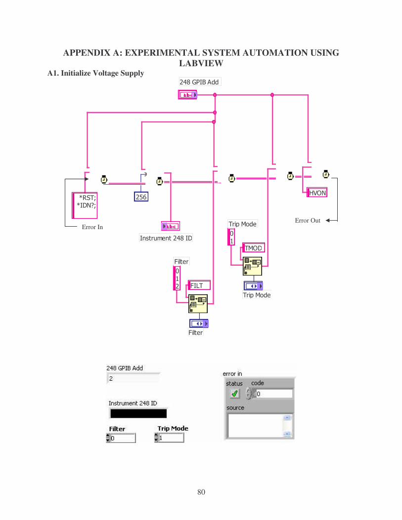
80
APPENDIX A: EXPERIMENTAL SYSTEM AUTOMATION USING LABVIEW
A1. Initialize Voltage Supply
#$%&'
()*(&+,*
-!#
&.
#/0
& #$%&+-!
1+
1
Error In Error Out

81
A2. Set Voltage Value
$
2 32
(4&*15,
) 67
#/08
9
!-
#$%&'
Error In Error Out
Current value of iteration
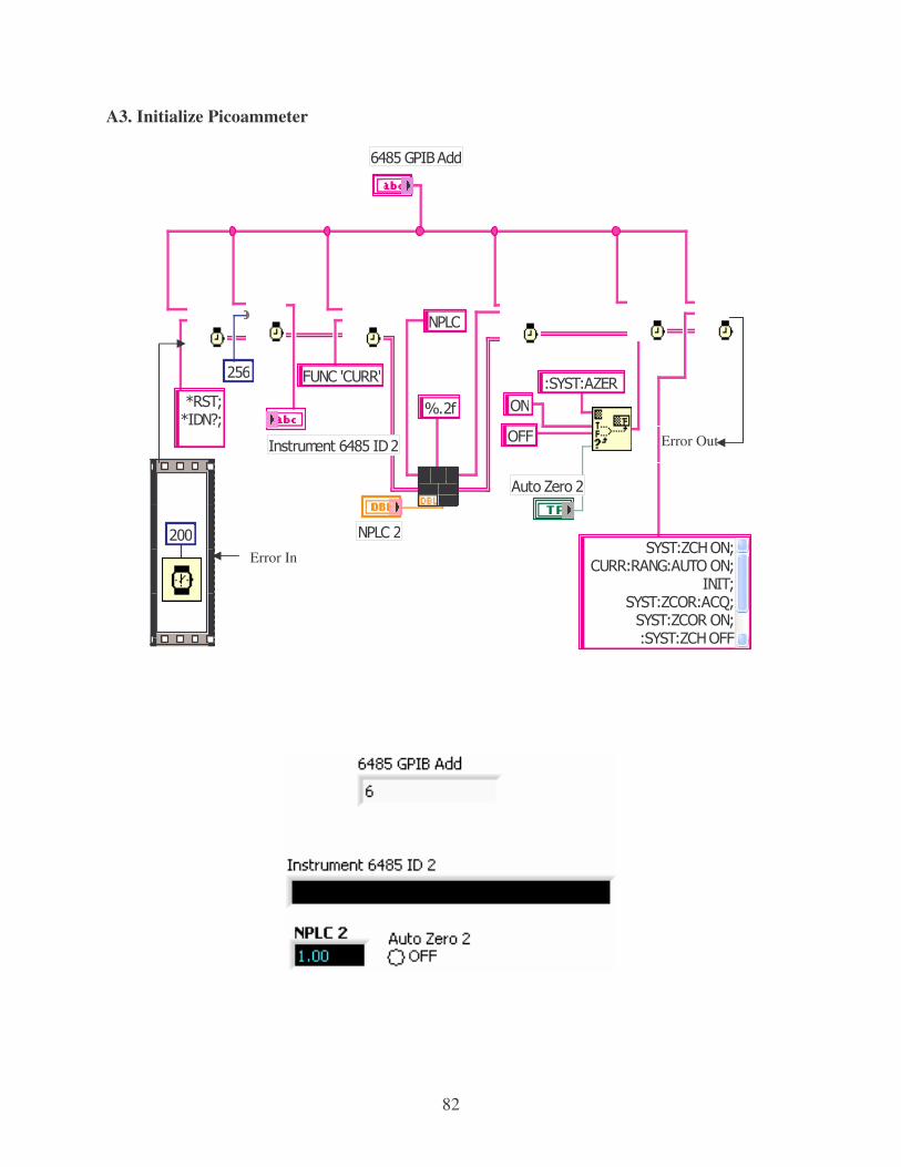
82
A3. Initialize Picoammeter
#--
()*(&+,*
9:#3
.#
.
5;5));#/0
& 0$%/&+#
1
1
<#
=>=<8)
>=<1*5))=)=511*
&&*>=<1)=?*>=<1)1*=>=<1
0$%/&'
Error In
Error Out

83
A4. Measure current
0$%/&'
8,
) 67
9:@
#/0&&
=1)=8.8)8+*
=>=<1
Error In
Error Out
84
A5. Create output data file and generate plots
&
9:@
67#
& 2#
&
#
$A%@-
3=
& 2@
!/--
#!B---
67

85

86
A6. Overview of the experimental process automation.
&
C
3=
0$%/&'
#$%&'
8-
Initialize High Voltage supply
Set Voltage Value
Initialize Picoammeter
Read Value of Field Emission Current
Create Output Date File
Generate Plots
87
APPENDIX B: TOOLS FOR DATA ANALYSIS DEVELOPED USING MATLAB
B.1 Program to generate multiple plots a=[];
b=[];
f=[];
[a]=xlsread('C:\abhilash\data\test.xls');
siz1 = size(a);
size1 = siz1(1,1);
for i=1:size1
if a(i,2)>0
a(i,4)=log(a(i,2)/((a(i,1)).^2));
a(i,3)=1/a(i,1);
end
end
j=1;
for i=1:size1
if (a(i,1)>1200)
f(j,1)=a(i,3);
f(j,2)=a(i,4);
j=j+1;
end
end
fsiz=size(f);
88
fsize=fsiz(1,1);
FNfit=polyfit(f(1:fsize,1),f(1:fsize,2),1);
p=exp(FNfit(1,2));
q=-1*FNfit(1,1);
for i=1:a(size1,1)
b(i,1)=i;
b(i,2)=p*i*i*exp((-1*q)/i);
b(i,3)=1/i;
b(i,4)=polyval(FNfit,1/i);
end
siz2 = size(b);
size2 = siz2(1,1);
scrsz = get(0,'ScreenSize');
figure('Position',[10 65 (3*scrsz(3)/4)+20 (3*scrsz(4)/4)+80]);
subplot(3,1,1); plot(a(1:size1,1),a(1:size1,2));...
xlabel('Voltage Applied(V)','FontSize',10);ylabel('Current Measured(A)','FontSize',10);grid
on;
subplot(3,1,2); plot(a(1:size1,3),a(1:size1,4),'.',b(50:size2,3),b(50:size2,4));...
xlabel('1/V','FontSize',10);ylabel('Ln(I / V^2)','FontSize',10); grid on;
subplot(3,1,3); plot(a(1:size1,1),a(1:size1,2),b(1:size2,1),b(1:size2,2),'.');...

89
xlabel('Voltage Applied(V)','FontSize',10);ylabel('Current Measured(A)','FontSize',10); grid
on;
h=gcf;
set(h,'Numbertitle','off');
set(h,'Name','GRAPHS');
set(h,'Papertype','A4');
B.2 Program for data analysis and curve fitting
%Current is in Amperes
%Area is in m2
%Work function is in electron volts
%Voltage is in Volts
%Inter-electrode distance is in m
%Field enhancement factor is a dimensionless quantity
clear;
format long e;
prompt = 'Please enter the complete path for the data (.xls) file',...
'Please enter the Inter-electrode distance (in m)',...
'Please enter the effective area of emission(in m2)',...
'Please enter notes if any';
dlg_title = 'Inputs required for data analysis';
num_lines= 2;
def = 'c:\Documents and Settings\Eashwar\My Documents\abhilash\data.xls',...

90
'0.000150',...
'0.0001','';
answer1 = inputdlg(prompt,dlg_title,num_lines,def);
r=[];
d=[];
a=[];
fn=[];
point=[];
j=1;
[r] = xlsread(char(answer1(1)));
r(any(isnan(r)'),:) = [];
d=str2double(char(answer1(2)));
a=str2double(char(answer1(3)));
siz1 = size(r);
size1 = siz1(1,1);
for i=1:size1
r(i,3)=r(i,1)/d;
if r(i,2)>0
fn(j,1)=1/r(i,3);
fn(j,2)=log(r(i,2)/((r(i,3)).^2));
91
j=j+1;
end
end
siz2 = size(fn);
size2 = siz2(1,1);
subplot(2,1,1); plot(r(1:size1,1),r(1:size1,2),'-or');...
xlabel('Voltage','FontSize',10);ylabel('Current','FontSize',10); grid on;
subplot(2,1,2); plot(fn(1:size2,1),fn(1:size2,2),'-og');...
xlabel('1/E','FontSize',10);ylabel('Ln(I / E^2)','FontSize',10); grid on;
prompt = 'Please enter the point where you want the fit to begin';
dlg_title = 'Inputs required for data analysis';
num_lines= 2;
def = '0.0000001577';
answer2 = inputdlg(prompt,dlg_title,num_lines,def);
point=str2double(char(answer2(1)));
j=1;
fnfit=[];
for i=1:size2
if (fn(i,1)<point)
fnfit(j,1)=fn(i,1);
fnfit(j,2)=fn(i,2);

92
j=j+1;
end
end
siz3=size(fnfit);
size3=siz3(1,1);
fnpolyfit=polyfit(fnfit(1:size3,1),fnfit(1:size3,2),1)
minval=min(fn(1:size2,1));
maxval=max(fn(1:size2,1));
j=maxval;
step=((maxval-minval)/1000);
fnpolyval=[];
for i=1:size3
fnpolyval(i,1)=fnfit(i,1);
fnpolyval(i,2)=polyval(fnpolyfit,fnfit(i,1));
end
siz4=size(fnpolyval);
size4=siz4(1,1);
93
subplot(1,1,1);plot(fnfit(1:size3,1),fnfit(1:size3,2),'-
*r',fnpolyval(1:size4,1),fnpolyval(1:size4,2),'-og');...
xlabel('1/E','FontSize',10);ylabel('Ln(I / E^2)','FontSize',10); grid on;
m=[];
c=[];
m=fnpolyfit(1,1);
c=fnpolyfit(1,2);
phi=[];
phi=0;
difference=1;
conv=[];
j=1;
change=1;
valnew=0;
while (change>0.0001)
phi=phi+0.01;
valold=valnew;
valnew=log(a*(0.0000015/phi)*((6440000000*((phi.^1.5)/m)).^2))+(10.4/(phi.^0.5));
difference=c-valnew;
change=abs(valold-valnew)

94
conv(j,1)=phi;
conv(j,2)=valnew;
j=j+1;
end
valnew
phi
gamma=-(6440000000*((phi.^1.5)/m))
siz5=size(conv);
size5=siz5(1,1);
subplot(1,1,1);plot(conv(1:size5,1),conv(1:size5,2),'-*r');...
xlabel('phi','FontSize',10);ylabel('val','FontSize',10); grid on;
clear;
95
APPENDIX C: PERMISSION TO USE COPYRIGHTED MATERIAL
C1.
From: "Jean-Marc Bonard" <[email protected]> To: "Abhilash Krishna" <[email protected]> Subject: Re: Permission to use figure Date: Mon, 20 Jun 2005 21:03:43 +0200 Dear Mr. Krishna, --------------------------------------------------------------- I am Abhilash Krishna, a master's student at Louisiana State University. My master's thesis is on Factors effecting field emission from MWNTs. For the purpose of adding in my thesis report, I would like to use the figure 5 in your research paper whose details are given below. Jean-Marc Bonard, Mirko Croci, Christian Klinke, fabien Conus, Imad Arfaoui, Thomas Stockli, and Andre Chatelain, “Growth of Carbon Nanotubes Characterized by field emission measurements during chemical vapor deposition”, Physical Review B 67, 085412 (2003). I would really appreciate if you could grant me the permission to use your figure. ------------------------------------------------------------------- There's absolutely no problem - please feel free to use the figure. And many thanks for your interest in our work! Good luck for your thesis, Kind regards, Jean-Marc Bonard
C2.
From: RIGHTS <[email protected]> To: [email protected] Subject: Re: Permission to use figure Date: Fri, 24 Jun 2005 12:09:26 -0400 Dear Abhilash Krishna: Thank you for requesting permission to reproduce material from American Institute of Physics and AVS The Science & Technology
96
Society publications. Permission is granted * as per the requirements indicated below * for the following: Figs. 2 and 3 S. C. Lim, H. J. Jeong, Y. S. Park, and D. S. Bae, Y. C. Choi, Y. M. Shin, W. S. Kim, K. H. An, and Y. H. Leea, "Field-emission properties of vertically aligned carbon-nanotube array dependent on gas exposures and growth conditions", J. Vac. Sci. Technol. A 19(4), Jul/Aug 2001, Fig. 4 Babu R. Chalamala and Robert H. Reuss, "Real-time measurement of pressure inside field-emission displays", Applied Physics Letters, Volume 79, Number 16, 2648-2650, 2001, Fig. 1 Shi-Dong Liang and N. S. Xua, "Chirality effect of single-wall carbon nanotubes on field emission", Applied physics letters volume 83, number 6, 11 August 2003, to be included in your master's thesis on "Factors effecting field emission from MWNTs" for Louisiana State University. 1. The following credit line must appear in all copies (please fill in the information indicated by CAPITAL LETTERS): Reprinted with permission from FULL CITATION. Copyright YEAR, American Institute of Physics. (Please use "AVS The Science and Technology Society" in place of "American Institute of Physics" when referencing the Journal of Vacuum Science and Technology material.) 2. Note: This permission does not apply to figures, tables or other materials credited to sources other than the copyright holder. 3. Obtain the Author's permission to use the materials. The author's address can be obtained from the article. Please let us know if you have any questions. Sincerely, Susann Brailey ~~~~~~~~~~~ Office of the Publisher, Journals and Technical Publications Rights & Permissions American Institute of Physics Suite 1NO1
97
2 Huntington Quadrangle Melville, NY 11747-4502 516-576-2268 TEL 516-576-2450 FAX [email protected] C3. From: "Otto Zhou" [email protected] To: "'Abhilash Krishna'" <[email protected]> Subject: RE: Permission to use figure Date: Thu, 23 Jun 2005 01:52:17 -0400 I hereby give you the permission to use the figure for your thesis report. Otto Zhou Lyle Jones Distinguished Professor Curriculum in Applied and Materials Sciences Department of Physics and Astronomy CB 3255 Phillips Hall Chapel Hill, NC 27599 Tel: 919-962-3297 FAX: 919-962-0480 email: [email protected] website: www.unc.edu/~zhou
-----Original Message----- From: Abhilash Krishna [mailto:[email protected]] Sent: Monday, June 20, 2005 2:12 PM To: [email protected] Subject: Permission to use figure
Dear Dr.Otto Zhou
I am Abhilash Krishna, a master's student at Louisiana State University. My master's thesis is on Factors effecting field emission from MWNTs.
For the purpose of adding in my thesis report, I would like to use the figure 4 in your research paper whose details are given below.
C.Bower, O.Zhou, W.Zhu, A.G.Ramirez, G.P.Kochanski, S.Jin, “Fabrication and field emission properties of carbon nanotube cathodes”, in: Amorphous & Nanostructures Carbon, Mat. Res. Soc. Symp. Proc., 2000. I would really appreciate if you could grant me the permission to use your figure.

98
Thank you very much for your time. Best Regards. Abhilash Krishna C4. From: "Yuan Cheng" [email protected] To: "AbhilashKrishna"<[email protected]> Subject: Re: Permission to use figure Date: Mon, 20 Jun 2005 15:29:49 -0400 Hi Abhilash, You can use the figure any way you want with full credit to the original publication. Thank you for your interest in my paper. Please feel free to contact me again if I can be of further assistance. best, Yuan Cheng ----- Original Message ----- From: Abhilash Krishna To: [email protected] Sent: Monday, June 20, 2005 2:32 PM Subject: Permission to use figure Dear Dr.Yuan Cheng
I am Abhilash Krishna, a master's student at Louisiana State University. My master's thesis is on Factors effecting field emission from MWNTs. For the purpose of adding in my thesis report I would like to use the figure 3 in your research paper whose details are given below.
Yuan Cheng, Otto Zhou, “Electron field emission from Carbon nanotubes”, C.R.Physique 4 (2003) 1021-1033. I would really appreciate if you could grant me the permission to use your figure. Thank you very much for your time. Best Regards. Abhilash Krishna
99
C5. From: "Zhifeng Ren" [email protected] To: "Abhilash Krishna" <[email protected]> Subject: Re: Permission to use figure Date: Wed, 22 Jun 2005 09:38:08 -0400 Yes, you can use them. Zhifeng At 05:31 PM 6/21/2005, you wrote: Dear Dr.Zhifeng Ren
I am Abhilash Krishna, a master's student at Louisiana State University. My master's thesis is on Factors effecting field emission from MWNTs. For the purpose of adding in my thesis report, I would like to use the figure 2 & 4 in your research paper whose details are given below.
D. Carnahan, M. Reed, Z. Ren, K. Kempa, Field emission from arrays of carbon nanotubes, NanoLab Inc., Physical sciences Inc., Boston college.
I would really appreciate if you could grant me permission the to use the figures
Thank you very much for your time.
Best Regards.
Abhilash Krishna
Zhifeng Ren, Professor Department of Physics Boston College Chestnut Hill, MA 02467 Phone: 617-552-2832 Fax: 617-552-8478 http://www.physics.bc.edu/faculty/Ren.html C6. From: "Bill Milne" [email protected] To: "Abhilash Krishna" <[email protected]> Subject: Re: Permission to use figure Date: Tue, 21 Jun 2005 08:42:38 +0100 Of course - please go ahead
100
Best of luck with your thesis Bill Milne At 20:14 20/06/2005, you wrote: Dear Dr. W. I. Milne I am Abhilash Krishna, a master's student at Louisiana State University. My master's thesis is on Factors effecting field emission from MWNTs. For the purpose of adding in my thesis report, I would like to use the figure 6 in your research paper whose details are given below. W.I. Milne, K.B.K. Teo, M.Chhowalla, G.A.J.Amaratunga, S.B.Lee, D.G.Hasko, H.Ahmed, O,Groening, P.Legagneux, L.Gangloff, J.P.Schnell, G.Pirio, D.Pribat, M.Castignolles, A.loiseau, V.Semet, Vu Thien Binh, "Electrical and field emission investigation of individual carbon nanotubes from plasma enhanced chemical vapour deposition", Diamond and Related materials 12 (2003) 422-428. I would really appreciate if you could grant me the permission to use your figure. Thank you very much for your time. Best Regards. Abhilash Krishna C7. From: "N S Xu" [email protected] To: "Abhilash Krishna" <[email protected]> Subject: Re: Permission to use figure Date: Wed, 22 Jun 2005 09:24:14 +0800 Yes. Thank you for letting me know. NSX ----- Original Message ----- From: "Abhilash Krishna" <[email protected]> To: [email protected] Sent: Tuesday, June 21, 2005 4:19 AM Subject: Permission to use figure
101
Dear Dr.N. S. Xu,
I am Abhilash Krishna, a master's student at Louisiana State University. My master's thesis is on Factors effecting field emission from MWNTs. For the purpose of adding in my thesis report, I would like to use the figure 1 in your research paper whose details are given below.
Shi-Dong Liang and N. S. Xua, “Chirality effect of single-wall carbon nanotubes on field emission” Applied physics letters volume 83, number 6, 11 august 2003. I would really appreciate if you could grant me the permission to use your figure. Thank you very much for your time. Best Regards. Abhilash Krishna C8. From: "Young Hee Lee" [email protected] To: "Abhilash Krishna" <[email protected]> Subject: Re: Permission to use figure Date: Tue, 21 Jun 2005 08:59:06 +0900 Dear Abhilash, Thank you for your interest on our paper. Sure you can use those figures anytime you would like to include your thesis. Best, Younghee Young Hee Lee, professor, Ph. D Department of Physics Center for Nanotubes and Nanostructured Composites Sungkyunkwan University Suwon, 440-746 Korea Tel: +82-31-299-6507, 290-5954(fax) email: [email protected] http://nanotube.skku.ac.kr/ ----- Original Message ----- From: Abhilash Krishna To: [email protected] Sent: Tuesday, June 21, 2005 5:30 AM Subject: Permission to use figure
102
Dear Dr. Y. H. Lee
I am Abhilash Krishna, a master's student at Louisiana State University. My master's thesis is on Factors effecting field emission from MWNTs. For the purpose of adding in my thesis report I would like to use the figures 2 and 3 in your research paper whose details are given below.
S. C. Lim, H. J. Jeong, Y. S. Park, and D. S. Bae, Y. C. Choi, Y. M. Shin, W. S. Kim, K. H. An, and Y. H. Lee, “Field-emission properties of vertically aligned carbon-nanotube array dependent on gas exposures and growth conditions”, J. Vac. Sci. Technol. A 19(4), Jul/Aug 2001. I would really appreciate if you could grant me the permission to use your figure. Thank you very much for your time. Best Regards. Abhilash Krishna C9. From: "Gupta, Sanju" <[email protected]> To: "Abhilash Krishna" <[email protected]> Subject: RE: Permission to use figure Date: Tue, 21 Jun 2005 01:37:04 -0500 You can cite the reference and provide necessary description and if really necessary, then use the Fig.3 in your thesis. Sincerely, ----------------------------------------------------------------------- Sanju Gupta (Ms), Ph.D Assistant Professor of Physics and Materials Science SW Missouri State University Kemper Hall, 103 M 901 South National Ave. Springfield, MO 65804 - 0027, USA T(O): +1-417-836-8565 F: +1-417-836-6226 E-mail: [email protected] Web mail: [email protected] Webpage: http://physics.smsu.edu/faculty/Gupta/research.htm C10. From: [email protected]

103
To: [email protected] Subject: Fw: Permission to use figure Date: Wed, 22 Jun 2005 15:09:54 +0100 Dear Abhilash Krishna Thank you for your permission request. Permission granted for the use requested. If material appears within our work with credit to another source, authorisation from that source must be obtained. Proper credit must be given to our publication. Credit must include the following components: Title of the Work, Author(s) and/or Editor(s) Name(s). Copyright year. Copyright John Wiley & Sons Limited. Reproduced with permission. Yours sincerely Duncan James Permissions Coordinator John Wiley & Sons, Ltd. 1 Oldlands Way Bognor Regis West Sussex PO22 9SA UK Tel: +44 (0) 1243 843356 Fax: +44 (0) 1243 770620 Email: [email protected] -----------Original Message from akrish2@lsuedu---------------------------- Dear Mr. Duncan James I am Abhilash Krishna, a master's student at Louisiana State University. My master's thesis is on Factors effecting field emission from MWNTs. For the purpose of adding in my thesis report I would like to use the figure 2(a)in the journal publication whose details are given below. T.Yamashita, K.Matsuda, T.Kona, Y.Mogami, M.Komaki, Y.Murata, and C.Oshima, Coherent electron emission from carbon nanotubes: asymmetric youngs interference fringes, Surface and Interface Analysis, 2003, Volume 35,Issue1, Pages 113-116. I will not be making more than 3 copies of my thesis report. I would really appreciate if you could grant me the permission to use this figure in my report.

104
Thank you very much for your time. Best Regards. Abhilash Krishna C11. From: "operator " [email protected] To: "Abhilash Krishna" <[email protected]> CC: "Jack Crummey" <[email protected]> Subject: RE: Permission to use picture Date: Mon, 20 Jun 2005 16:45:17 -0700 Hello Sir, We would be happy to allow use of the pictures on our website for your project. What we ask is that you accredit our facility wherever these pictures will be used. If you have any other questions please feel free to contact me. Best Regards, Alicia Smurphat Customer Service Manager Huntington Mechanical Labs Tel: (650) 964-3323 x10 Fax: (650) 964-6153 Email: [email protected] -----Original Message----- From: Abhilash Krishna [mailto:[email protected]] Sent: Monday, June 20, 2005 2:28 PM To: operator Subject: Permission to use picture
Dear Madam,
I am Abhilash Krishna, a master's student at Louisiana State University. My master's thesis is on Factors effecting field emission from MWNTs.
For the purpose of adding in my thesis report, I would like to use the picture of the Linear motion feedthrough L2141 series found on your company website mentioned below.
http://209.238.89.157/series.asp?series=L-2141 I would really appreciate if you could grant me the permission to use your figure. Thank you very much for your time. Best Regards.
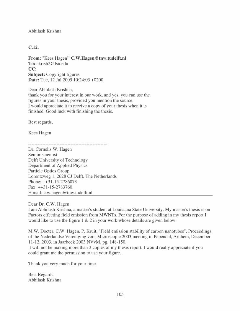
105
Abhilash Krishna C.12. From: "Kees Hagen" [email protected] To: [email protected] CC: Subject: Copyright figures Date: Tue, 12 Jul 2005 10:24:03 +0200
Dear Abhilash Krishna, thank you for your interest in our work, and yes, you can use the figures in your thesis, provided you mention the source. I would appreciate it to receive a copy of your thesis when it is finished. Good luck with finishing the thesis. Best regards, Kees Hagen -------------------------------------------------- Dr. Cornelis W. Hagen Senior scientist Delft University of Technology Department of Applied Physics Particle Optics Group Lorentzweg 1, 2628 CJ Delft, The Netherlands Phone: ++31-15-2786073 Fax: ++31-15-2783760 E-mail: [email protected] Dear Dr. C.W. Hagen I am Abhilash Krishna, a master's student at Louisiana State University. My master's thesis is on Factors effecting field emission from MWNTs. For the purpose of adding in my thesis report I would like to use the figure 1 & 2 in your work whose details are given below. M.W. Docter, C.W. Hagen, P. Kruit, "Field emission stability of carbon nanotubes", Proceedings of the Nederlandse Vereniging voor Microscopie 2003 meeting in Papendal, Arnhem, December 11-12, 2003, in Jaarboek 2003 NVvM, pg. 148-150. I will not be making more than 3 copies of my thesis report. I would really appreciate if you could grant me the permission to use your figure. Thank you very much for your time. Best Regards. Abhilash Krishna

106
C.13.
30 June 2005 Our ref: HG/smc/June 2005.jl693 Dear Mr Krishna DIAMOND AND RELATED MATERIALS, Vol 12, No 1, 2003, Pages 422-428, Milne et al, ‘Electrical and …’, 1 Figure only As per your letter dated 20 June 2005, we hereby grant you permission to reprint the aforementioned material at no charge in your thesis subject to the following conditions: 1. If any part of the material to be used (for example, figures) has appeared in our publication
with credit or acknowledgement to another source, permission must also be sought from that source. If such permission is not obtained then that material may not be included in your publication/copies.
2. Suitable acknowledgment to the source must be made, either as a footnote or in a reference
list at the end of your publication, as follows:
“Reprinted from Publication title, Vol number, Author(s), Title of article, Pages No., Copyright (Year), with permission from Elsevier”.
3. Reproduction of this material is confined to the purpose for which permission is hereby
given. 4. This permission is granted for non-exclusive world English rights only. For other languages
please reapply separately for each one required. Permission excludes use in an electronic form. Should you have a specific electronic project in mind please reapply for permission.
5. This includes permission for UMI to supply single copies, on demand, of the complete
thesis. Should your thesis be published commercially, please reapply for permission. Yours sincerely
Helen Gainford (Rights Manager)
107
VITA
The author, Abhilash Krishna was born in December 1980, in Andhra Pradesh, India. He
graduated from Little Flower Junior College, Hyderabad, in 1998. In September 1998, the author
attended Jawaharlal Nehru Technological University, Hyderabad, India, with a major in
electronics and communications engineering. He obtained a Bachelor of Technology degree in
electronics and communications engineering in May 2002. He continued his graduate study in
electrical and computer engineering at Louisiana State University where he is currently a
candidate for the degree of Master of Science in Electrical Engineering.