fabrication of electro optical nano modulator on silicon chip
TRANSCRIPT

Microelectronic Engineering 86 (2009) 1099–1102
Contents lists available at ScienceDirect
Microelectronic Engineering
journal homepage: www.elsevier .com/locate /mee
Fabrication of electro optical nano modulator on silicon chip
Ofer Limon a,*, Luca Businaro b, Annamaria Gerardino c, Liora Bitton d, Aviad Frydman d, Zeev Zalevsky a
a School of Engineering, Bar-Ilan University, 52900 Ramat Gan, Israelb CNR – National Inst. for Matter Physics (INFM), TASC Laboratory, Trieste, Italyc CNR – Inst. for Photonics and Nanotechnologies (IFM), Rome, Italyd Jack and Pearl Resnick Institute of Advanced Technology, Physics Dept., Bar-Ilan University, Ramat Gan, Israel
a r t i c l e i n f o
Article history:Received 29 September 2008Received in revised form 17 November 2008Accepted 9 January 2009Available online 17 January 2009
Keywords:Electro optical modulatorSilicon chipNano particleIntegrated optics
0167-9317/$ - see front matter � 2009 Elsevier B.V. Adoi:10.1016/j.mee.2009.01.007
* Corresponding author. Tel.: +972 522314738; faxE-mail address: [email protected] (O. Limon).
a b s t r a c t
In this paper, we present the fabrication and preliminary measurements of a novel electro optical nanomodulator on silicon chip based on light scattering by a movable 50 nm charged gold colloid particle.The idea is to modulate the 1.55 lm light by electrically manipulating the highly conductive particlein a nano air gap created in a silicon waveguide to cause high scattering and absorption. With a lengthof 150 nm of the air gap, the expected modulation rates can exceed few GHz while being implementedon a highly dense silicon chip.
� 2009 Elsevier B.V. All rights reserved.
1. Introduction
Due to the optical communication revolution that we have beenwitnessing for the last two decades, the need for a modulator thatwill allow direct communication between the electronics comput-ers and the optical communication has grown substantially. Fur-thermore, the internal on board metal connection existing todayare facing their physical boundaries while optical on board com-munication may allow faster calculations and communicationrates [1]. Integration between the standard microelectronics, basedon silicon CMOS technology, and micro scale optical devices are anecessary condition for high-speed optical on board communica-tion and it is acting today as driving force for developing siliconphotonics platforms. Couplers, splitters, amplifiers, low loss wave-guides, light emitters, adders and filters [2] on silicon have beendemonstrated, but a micro scale low power dissipating and highrate modulators are still challenging goals. In order to realize anelectro optical modulator on silicon chip, one has to overcomethe weak electro optical interaction in silicon [3]. Some have dealtwith this issue by producing very long structures [4], others havemade short devices using a ring resonator [5] which has a high fi-nesse and narrow spectral response. The device described in thispaper does not use the inherent electro optical properties of siliconbut rather uses an implantation of a nano gold particle to modulatethe light.
ll rights reserved.
: +972 774422038.
The operation principle is based on a novel design of a capacitor.A single mode silicon waveguide leads the wave into a SiO2 widerregion; a nano air hole has been produced inside the SiO2 and twogold contacts were placed at each side of the capacitor to enable anelectrical field within the SiO2 region; finally a charged nano goldparticle is displaced within the air gap by the electric field gener-ated in the capacitor.
When we couple light from an external light source like a ta-pered fiber carrying a 1.55 lm signal into the single mode siliconwaveguide, the output energy is strongly correlated to the positionof the gold particle inside the air gap. If the gold particle is set atthe lower part of the air gap (Fig. 1a), the light from the inputwaveguide passes right through to the output waveguide. Whenwe apply a voltage on the capacitor contacts, the inner electricalfield attracts or repels the charged nano gold particle. When thegold particle is placed inside the optical path, most of the energyis scattered and absorbed by the highly conductive particle andtherefore the output energy is substantially decreased.
2. Simulations
To verify our assumption and to design an efficient electro opti-cal modulator we used COMSOL Multyphysics to solve the partialwave equations for the proposed device:
r� ðl�1r r� EzÞ � ðer � jr=xe0Þk2
0Ez ¼ 0 ð1Þ
where lr is the relative magnetic permeability, Ez is the transverse Zcomponent of the electric field, er is the dielectric coefficient, r is
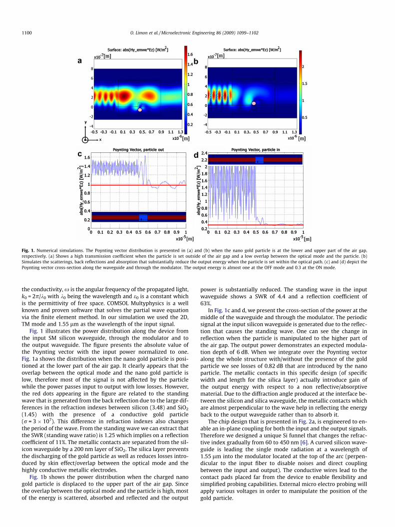
Fig. 1. Numerical simulations. The Poynting vector distribution is presented in (a) and (b) when the nano gold particle is at the lower and upper part of the air gap,respectively. (a) Shows a high transmission coefficient when the particle is set outside of the air gap and a low overlap between the optical mode and the particle. (b)Simulates the scatterings, back reflections and absorption that substantially reduce the output energy when the particle is set within the optical path. (c) and (d) depict thePoynting vector cross-section along the waveguide and through the modulator. The output energy is almost one at the OFF mode and 0.3 at the ON mode.
1100 O. Limon et al. / Microelectronic Engineering 86 (2009) 1099–1102
the conductivity, x is the angular frequency of the propagated light,k0 = 2p/k0 with k0 being the wavelength and e0 is a constant whichis the permittivity of free space. COMSOL Multyphysics is a wellknown and proven software that solves the partial wave equationvia the finite element method. In our simulation we used the 2D,TM mode and 1.55 lm as the wavelength of the input signal.
Fig. 1 illustrates the power distribution along the device fromthe input SM silicon waveguide, through the modulator and tothe output waveguide. The figure presents the absolute value ofthe Poynting vector with the input power normalized to one.Fig. 1a shows the distribution when the nano gold particle is posi-tioned at the lower part of the air gap. It clearly appears that theoverlap between the optical mode and the nano gold particle islow, therefore most of the signal is not affected by the particlewhile the power passes input to output with low losses. However,the red dots appearing in the figure are related to the standingwave that is generated from the back reflection due to the large dif-ferences in the refraction indexes between silicon (3.48) and SiO2
(1.45) with the presence of a conductive gold particle(r = 3 � 107). This difference in refraction indexes also changesthe period of the wave. From the standing wave we can extract thatthe SWR (standing wave ratio) is 1.25 which implies on a reflectioncoefficient of 11%. The metallic contacts are separated from the sil-icon waveguide by a 200 nm layer of SiO2. The silica layer preventsthe discharging of the gold particle as well as reduces losses intro-duced by skin effect/overlap between the optical mode and thehighly conductive metallic electrodes.
Fig. 1b shows the power distribution when the charged nanogold particle is displaced to the upper part of the air gap. Sincethe overlap between the optical mode and the particle is high, mostof the energy is scattered, absorbed and reflected and the output
power is substantially reduced. The standing wave in the inputwaveguide shows a SWR of 4.4 and a reflection coefficient of63%.
In Fig. 1c and d, we present the cross-section of the power at themiddle of the waveguide and through the modulator. The periodicsignal at the input silicon waveguide is generated due to the reflec-tion that causes the standing wave. One can see the change inreflection when the particle is manipulated to the higher part ofthe air gap. The output power demonstrates an expected modula-tion depth of 6 dB. When we integrate over the Poynting vectoralong the whole structure with/without the presence of the goldparticle we see losses of 0.82 dB that are introduced by the nanoparticle. The metallic contacts in this specific design (of specificwidth and length for the silica layer) actually introduce gain ofthe output energy with respect to a non reflective/absorptivematerial. Due to the diffraction angle produced at the interface be-tween the silicon and silica waveguide, the metallic contacts whichare almost perpendicular to the wave help in reflecting the energyback to the output waveguide rather than to absorb it.
The chip design that is presented in Fig. 2a, is engineered to en-able an in-plane coupling for both the input and the output signals.Therefore we designed a unique Si funnel that changes the refrac-tive index gradually from 60 to 450 nm [6]. A curved silicon wave-guide is leading the single mode radiation at a wavelength of1.55 lm into the modulator located at the top of the arc (perpen-dicular to the input fiber to disable noises and direct couplingbetween the input and output). The conductive wires lead to thecontact pads placed far from the device to enable flexibility andsimplified probing capabilities. External micro electro probing willapply various voltages in order to manipulate the position of thegold particle.

Fig. 2. (a) The chip design introduces a funnel which is a silicon waveguide that isused as a coupler and a medium for mode matching between external tapered fiberand internal single silicon (SM) waveguides. The modulator is positioned at the topof the SM silicon waveguide arc. Large electrical contacts are placed to enablesimple operation and connection of micro electro probes. (b) SEM images of thefabricated device; enlarged images of the modulator and the Si funnel tip.
O. Limon et al. / Microelectronic Engineering 86 (2009) 1099–1102 1101
3. Fabrication
The device was fabricated starting from a 200 nm Si/2 lm SiO2
Silicon On Insulator (SOI) wafer by means of three aligned electronbeam lithographic processes using a LEICA-VISTEC EBPG-5 100KeVmachine. Having defined the aligning markers using optical lithog-raphy followed by the deposition of 10 nm Ti/60 nm Au by thermalevaporation and lift-off, the first step in the patterning of the singlemode waveguides was accomplished. This has achieved writing thewaveguide structures on a 150 nm thick negative resist (DowCorning FOX-12 HSQ resist, dose 1000 lC/cm2 for the lower reso-lution structures) which has been used as a masking layer for thesubsequent silicon etching by means of chlorine based 5 min reac-tive ion etching (RIE) process (Cl2 30 sccm Ar 20 sccm, RF power170 W, Pressure 100 mTorr, self bias 140 V using a Oxford Plasma-lab 80 machine). For the second step, i.e. the realization of the insu-lating containing box for the metal nano particle, we decided to useagain the HSQ resist which, after exposure and development,becomes similar to silica (SiOx, where x is between 1.5 and 2).The third step which included the realization of the electrical con-tacts, has been obtained again by an aligned electron beam lithog-raphy on a 1 lm thick positive resist (micro resist UVIII, dose22 lC/cm2) followed by the deposition of a 10 nm Ti/60 nm Aumetallic bilayer by evaporation and lift-off. The details of the ob-tained device are presented in Fig. 2b.
4. Experimental testing
In order to position the nano gold particle in the air gap, the fol-lowing steps have been accomplished: We use colloidal goldunconjugated particles which are produced with a size distributionof 30 ± 3 nm. The nanoparticles are in a water solution and theoverall net charge on the colloidal particle surfaces is negative. Inorder to connect these particles to the surface we use an organic
layer, called Poly-L-Lysine (P-L-L) which is positively charged andthus acts as an adhesive layer. First we deposit Poly-L-Lysine byplacing a drop on the SiO2 wafer. The P-L-L is electrostatically con-nected to the surface and after drying the residues we drop few mi-cro liters of gold nanoparticles solution on it and the negativecharge is electrically connected to the positive charge of thePoly-L-Lysine. Our method allows us to control the particles den-sity very easily. This is presented in Fig. 3a.
We used a non feedback method of the AFM (atomic forcemicroscope) to displace a single nano particle from the SiO2 tothe air gap. Fig. 3a and b show a nano gold particle that is posi-tioned right on the edge of the nano air gap a moment before itwas pushed inside. A parallel approach to be used for a chip con-taining many such modulators can allow positioning plurality ofparticles in the gaps by a unique polymer that connects exclusivelyon the one hand to the gold particle and on the other hand to aunique material. Following a process of lithography may allowremoval of this material from the chip except from the air gapslocations which eventually will yield a selective assignment ofthe particles only to the gaps in a parallel methodology.
By using micro electro probing, we applied various voltages inthe range of several volts on the SiO2 capacitor to manipulate theposition of the particle in the air gap by changing the inner electri-cal field.
The best results that we have received for several devices wereobtained for voltages around a 10 V DC input. Much lower voltagesand time dependant pulses are yet to be examined. In Fig. 3c and done may see the single nano gold particle that is located in the airgap before and right after applying the electrical field. We demon-strate a measured shift of at least 20 nm in the air gap. This shiftallows us to modulate the light that goes right through it. Sincethe modulation rate is determined by the required shift of the nanoparticle while this shift should be small (only a few tens of nanometers) and since the particle has high mobility inside the airgap due to the contracting polymer, we expect a high modulationrate and very low power dissipation. The estimation of the modu-lation rate can be derived from the time that takes a chargedsphere particle to pass a given distance between the capacitor’splates due to the applied electrical force. Assuming a simplifiedmodel in which the particle has zero initial velocity the time esti-mation is:
T ¼ffiffiffiffiffiffi2La
r¼
ffiffiffiffiffiffiffiffiffiffiffiffi2Ldm
VQ
s¼ R
ffiffiffiffiffiffiffiffiffiffiffiffiffiffiffiffi2Ldq
3e0VV0
sð2Þ
where L is the length of the shift, a is the acceleration of the particle,d is the distance between the capacitor plates, m is the mass of theparticle, V is the applied voltage on the capacitor electrodes, Q is thecharge of the particle, R is the radius of the particle, q is the massdensity of the particle, V0 is the voltage at which the particle wascharged and e0 = 8.85 � 10�12 [F/m]. For a gold particle withR = 15 nm, q = 19,300 [kg/m3] and d = 150 nm, L = 30 nm, that wascharged at V0 = 200 [v] while applying a voltage of V = 10 [v] onthe capacitor, one obtains T = 0.85 [ns].
5. Conclusion
We proposed a unique electro optical modulator that is basedon a manipulation of a highly scattering and absorbing nano goldparticle inside a nano air gap. This kind of modulator can be imple-mented on a highly dense silicon chip and be integrated with othermicroelectronics on die. We showed the numerical simulationsthat led us to design an efficient modulator with nano scale geom-etries. The fabrication process of the modulator was described andproven to be feasible. Our preliminary measurements have verifiedthe feasibility for shifting the gold particle inside the air gap. The

Fig. 3. AFM images demonstrating a randomly scattered deposition of nano gold particles near the air gap ((a) and (b)) and a single gold particle which was shifted by 20 nmin the air gap due to inner electrical field that was applied by external voltage connected to the electrical contacts of the modulator ((c) and (d)).
1102 O. Limon et al. / Microelectronic Engineering 86 (2009) 1099–1102
overall nano scale modulator may allow the full integration be-tween input/output optical signals and electrical control com-mands while allowing silicon on chip modulation with GHzrange rates.
References
[1] C. Luo, J.D. Joannopoulos, S. Fan, Opt. Lett. 28 (2003) 637–639.
[2] Y.A. Vlasov, S.J. McNab, Opt. Express 12 (2004) 1622–1631.[3] R.A. Soref, B.R. Bennett, IEEE J. Quant. Elec. 23 (1987) 123–129.[4] A. Liu, R. Jones, L. Liao, D. Samara-Rubio, D. Rubin, O. Cohen, R. Nicolaescu, M.
Paniccia, Nature 427 (2004) 615–618, doi:10.1038/nature02310.[5] V.R. Almeida, C.A. Barrios, R.R. Panepucci, M. Lipson, Nature 431 (2004) 1081–
1084.[6] V.R. Almeida, R.R. Panepucci, M. Lipson, Opt. Lett. 28 (2003) 1302–1304.