fabrication and characteristics of microwave backward diodes in
TRANSCRIPT
LOAN COPY: RETURN TO AFWL (WLDL-2)
KiRTLANO AFB, N MEX
FABRICATION A N D CHARACTERISTICS OF MICROWAVE BACKWARD DIODES IN INDIUM ARSENIDE
by John B. Hopkins
Electronics Reseurch Center Cumbridge, Mass.
N A T I O N A L A E R O N A U T I C S A N D SPACE A D M I N I S T R A T I O N W A S H I N G T O N , D . C. S E P T E M B E R 1 9 6 9 ,
https://ntrs.nasa.gov/search.jsp?R=19690027328 2018-02-13T08:37:57+00:00Z

i TECH LIBRARY KAFB,NM
1. Report No. I 2. Government Accession No. 1 3. Recipient's Catalog NO.
NASA TN D-5401 4. T i t l e and Subtitle Fabrication and 5. Report Date
September 1969Characteristics of Microwave 6. Performing Organization Code
Backward Diodes in Indium Arsenide 7. Authods) 8. Performing Orgonization Report NO. John B. Hopkins c-77
9. Performing Organization Name and Address 10. Work Uni t No.
125-21-03-11 Electronics Research Center 11. Contract or Grant No.
Cambridge, Massachusetts, 02139 ! 13. Type of Report and Period Covered
2. Sponsoring Agency Name and Address Technical Note
National Aeronautics and SpaceAdministration I14. Sponsoring Agency Code
1
15. Supplementary Notes
\
17. Key Words ( S u g g e s t e d b y A u t h o t ( s ) ) 18. Distribution Stotement
Depleted Uranium Radiation Shield Unclassified - unlimited Lithium Hydride Tungsten
19. Security Classif. (of this report) 20. Security Classif . (of this page) [ 21. No. of Pages 22. Pr ice*
Unclassified Unclassified 17 I $3.00
*For sale by the Clearinghouse for FederalScientific and TechnicalInformation Springfield,Virginia 22151
f
FABRICATION AND CHARACTERISTICS OF MICROWAVE
BACKWARD DIODES IN INDIUM ARSENIDE
By John B. Hopkins Electronics Research Center
Cambridge, Massachusetts
SUMMARY
Analysis and calculations have been carried out supportingthe initial qualitative judgment that microwave backward diodes fabricated from InAs will have significant advantages over currently used materials, particularly in the area of reliability. An experimental program including fabrication and characterization of such diodes has been undertaken. Microwave (9 GHz) diodes of adequate quality have been constructed, although etching procedures are not as yet sufficiently refined to provide junctions with area as small as desired, particularly on a reproducible basis. This has provided confirmation for the prediction that good microwave back diodes can be producedin InAs, for substantially larger junctions than used in Ge back diodes, with consequent reliability improvements. These results also tend to support the result that improvement in sensitivity at a specified frequency, or in cutoff frequency, can be expected, although improvement in this sphere is less dramatic. The principal drawback of the InAs diodes, resultingfrom the low bandgap, is the limitation in maximum operating temperature, for diffusion current becomes comparable to tunnel current (with deleterious egfects on performance) for an ambient temperature of 2 5 to 3 5 C . (This effect could be countered through moderate cooling, possibly thermoelectric.)The InAs diode is already attractive for applications where only lower temperatures are to be encountered, as there is litgle change in its microwave characteristic between 80 and 3 0 0 K.
On theoretical grounds, a substantially greater bandgapcould be obtained without seriously compromising the effective mass by use of the ternary compound semiconductor indium arsenide-phosphide, although this single application does not appear to warrant the material development effort that would be necessary.

INTRODUCTION
The back diode, a variant of the tunnel diode, has existed since the development of the tunnel diode began ten years ago.Originally, interest in the tunnel diode was based on the existence of a negative-resistance region in the current-voltagecharacteristic, making possible particularly simple amplifiers,oscillators, and bistable circuits for computer applications. As is often the case, various limitations have prevented the tunnel diode from achieving the dominance first anticipated, but it remains one of the more important solid-state electronic devices. An application for which the tunnel diode has been considered with increasing interest in recent years is microwave detection and mixing (refs. 1-5). ,Whenbiased to a current near Ip, the peak current, extremely high sensitivity can be obtained, unfor- &
tunately accompanied by limited dynamic range, high capacitance,undistinguished low-frequency noise performance, and the need for a stable biasing circuit. These diodes, which are valuable for certain applications, are complemented by a special form of tunnel diode, the back diode microwave detector, which has also been the object of rising interest for several years (refs. 6-10), and has recently become available commercially from a number of manufacturers.
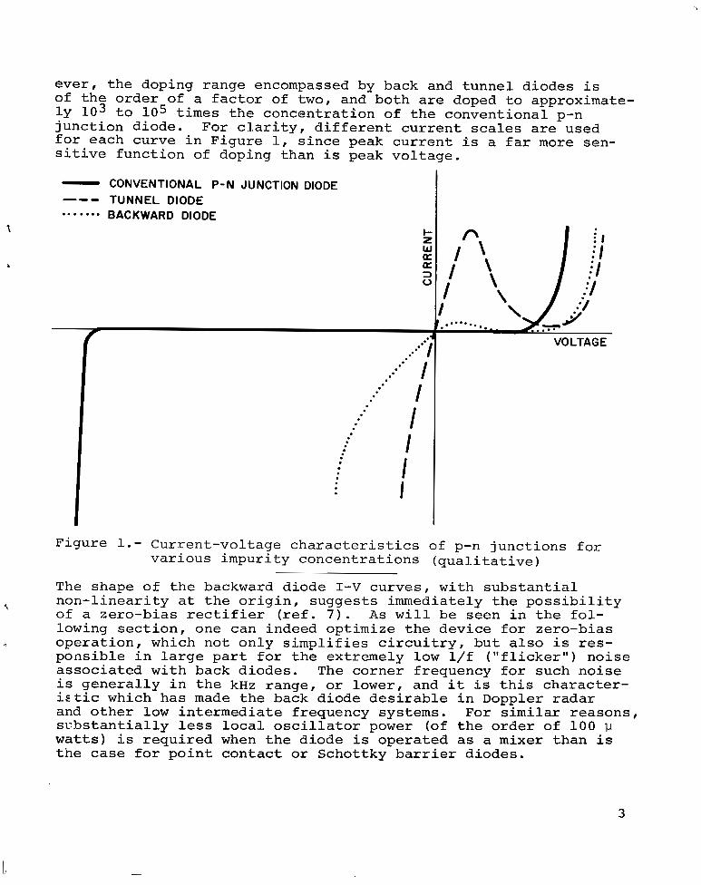
There is some imprecision in the definition of a back (or"backward") diode. An idealized back diode is usually thought of as a tunnel diode with impurity concentrations such that band overlap (with consequent flow of tunnel current) ceases at zero applied voltage. One then sees normal diffusion current, which is very small for low voltage, in the forward direction, with rather higher tunnel current in the reverse direction. Such a diode exhibits reversal of the usual "soft" and "hard"(l'low"and high-resistance) directions, and was thus given the name "back", or "backward",diode. However, for slightly higher impurity concentrations one obtains a tunnel diode with reverse current markedlyincreased over this ''pure" back diode but still exhibiting quitelow peak voltage and peak current, and large negative resistance, which are of no importance in most applications. These last three characteristics are the ones generally intended when the name "back diode" is applied. Figure 1 shows qualitatively that the range of characteristics one sees as impurity concentration is varied, going from a conventional diode to a tunnel diode*. How-
*A particularly clear demonstration of this dependence is given byLesk, et al., 1959 I R E Wescon Convention Record, Pt. 3 , pp. 9-31.
2
7
--- 'I
b
'\
ever, the doping range encompassed by back and tunnel diodes is of the order of a factor of two, and both are doped to approximately l o 3 to lo5 times the concentration of the conventional p-njunction diode. For clarity, different current scales are used for each curve in Figure 1, since peak current is a far more sensitive function of doping than is peak voltage.
-CONVENTIONAL P-N JUNCTION DIODE TUNNEL DIODE ....... BACKWARD DIODE
Iz w a p: 3 0
VOLTAGE
I I I I
Figure 1.- Current-voltage characteristics of p-n junctions for various impurity concentrations (qualitative)
The shape of the backward diode I-V curves, with substantial non-linearity at the origin, suggests immediately the possibilityof a zero-bias rectifier (ref. 7 ) . As will be seen in the following section, one can indeed optimize the device for zero-bias operation, which not only simplifies circuitry, but also is responsible in large part for the extremely low l/f ("flicker")noise associated with back diodes. The corner frequency for such noise is generally in the kHz range, or lower, and it is this characteriEtic which has made the back diode desirable in Doppler radar and other low intermediate frequency systems. For similar reasons, substantially less local oscillator power (of the order of 100 LI watts) is required when the diode is operated as a mixer than is the case for point contact or Schottky barrier diodes.
3

The substantial tunneling current means that the device will have significantly lower impedance than conventional detectors, which is an advantage in most cases, simplifying matching to typical systems, and permitting broad bandwidths. (It is partiallyfor the reduction of video resistance that other types of diodes require bias, which is detrimental to noise performance). The insensitivity of tunnel currents to temperature and radiation is an added benefit. However, the back diode is not without disadvantages. Tunneling junctions are generally of the order of 100 A in thickness, and this leads to high junction capacitance with associated problems for high-frequency systems. Along with the rdesirable low barrier resistance, one must accept susceptability to damage from large transient voltages, and only fair burnout resistance. Also, the barrier resistance can be too low, erring b
in the opposite direction.
One means of minimizing or removing these weaknesses is through the choice of an appropriate material for diode fabrication. Increasing use and availability of a number of 111-V compound semiconductors makes this a reasonable approach, and givesvalidity to an analysis aimed at determination of an optimummaterial. Such an analysis follows.
SYMBOLS
dn, dp Depletion width, n and p regions
Ey Energy of top of valence band, p-region
Ec
E Energy band gapg
Energy of bottom of conduction band, n-region
fn, fp Fermi functions, n and p regions
h Planck's constant
idc
IP
It
DC junction current
Peak current
Tunnel current
k Boltzman constant
m* Reduced effective mass
'rf RF power incident on diode
Pt Tunneling probability
4

-1
9 Electronic charge
r Junction radius
pv Density of states, conduction, and valence bands
0 Electrical conductivity
T Temperature
VP Peak voltage t
CHOICE OF OPTIMUM MATERIAL b'
Outline of Calculations
As a first step, one can obtain a very simple measure of the appropriateness of a particular semiconducting material to tunneling applications by examination of the basic expression for tunneling probability. The quantum-mechanical result for a simpletriangular potential barrier of height E
El can be expressed as
Pt cc exp 1 [..;.l[.*Eg]' 2 h I (1)
Due to the minus sign, this probability will be higher for smaller (m* Eg). Of course, tunneling currents may be estimated from a rather more complex equation, with multipliers includingthese and other parameters. However, the exponential dependencemakes this term by far the most important for a first approximation. For device applications, high tunneling probability is of considerable importance, and it is particularly useful in the case of microwave diodes. As mentioned previously, the extreme narrowness of tunneling junction leads to high junction capacitance and consequent frequency limitations. For larger Pt, a given tunneling current will be obtained for smaller area (if doping is held constant) or for a lower-doping (wider) junction (for unchangedarea). Thus, increasing Pt should be a significant step in device improvement. Table 1 shows values of m*, E and (m*Eg)$for a number semiconductors. By far the smallest ?A* Eg) is found for InSb, but with a bandgap of .17 eV, room temperatureoperation is out of the question. InAs is the next most promising, and here there is clearly a real possibility of meaningfuldevice improvement. (A similar analysis is carried out byKleinknect (ref. ll), with the same basic result). However, there are several reasons for carrying out a more elaborate analysisof the situations. The relationship between material parametersand meaningful indicators of microwave performance-current sensitivity, cutoff frequency, noise equivalent power (NEP, closely
5
7

related to tangential sensitivity), and others - is a rather complex one, and only limited confidence can be placed in simpleapproximations. Further, before undertaking the effort involved in trying a new material, it is important to have a good estimate of the magnitude and type of improvement which should be obtainable. Finally, it is useful to have an indication of necessary or optimum values of fabrication parameters - in particular,impurity doping concentrations and junction area.
Although the individual parts of such calculations are quite straightforward, the number of different steps involved, along iwith the necessity of using techniques of iteration and numerical analysis, and the number of times such calculations must be repeated for different parameter values, make mandatory the use of b
a fast digital computer. Given the availability of such a machine, one can easily consider not only materials which are alreadyavailable, but also those which might become available, such as mixed 111-V compounds of various proportions.
The details of the calculation have been given elsewhere, (ref. 12) and will only be outlined here and summarized in the appendix. For a given material, the temperature and various physical constants are specified, as are doping concentrations and impurity levels and junction area (m2). The Fermi levels in both the p and n regions are determined in conventional fashion from the charge neutrality condition, with careful evaluation of Fermi integrals and an iterative solution of the transcendental equation. This permits evaluation of carrier concentrations, resistivity, etc. Then, under the assumption of an abrupt junction, depletion width (dn + dp), capacitance, diffusion current, and other junction parameters are determined. Tunnel current is calculated for specific applied voltages, according to conventional equations.
In the computer program, an iterative approach is used first to calculate the peak current and voltage. (The peak voltage is a useful parameter with which to characterize the doping level of the diode, since it is easily measured.) One can then calculate
i. any desired points for a complete I-V curve. For estimation of microwave detection parameters, the points for which calculations are carried out are for +1 and +2 mV on both sides of any desired i bias point (usually zero). Numerical analysis may then be used to determine the slope (f') and curvature (f") of the current-voltage graph, i=f(v). Then microwave figures of merit are readily calculated:
f"DC Current Sensitivity = 6 E-idc
= 4 'rf f'
6
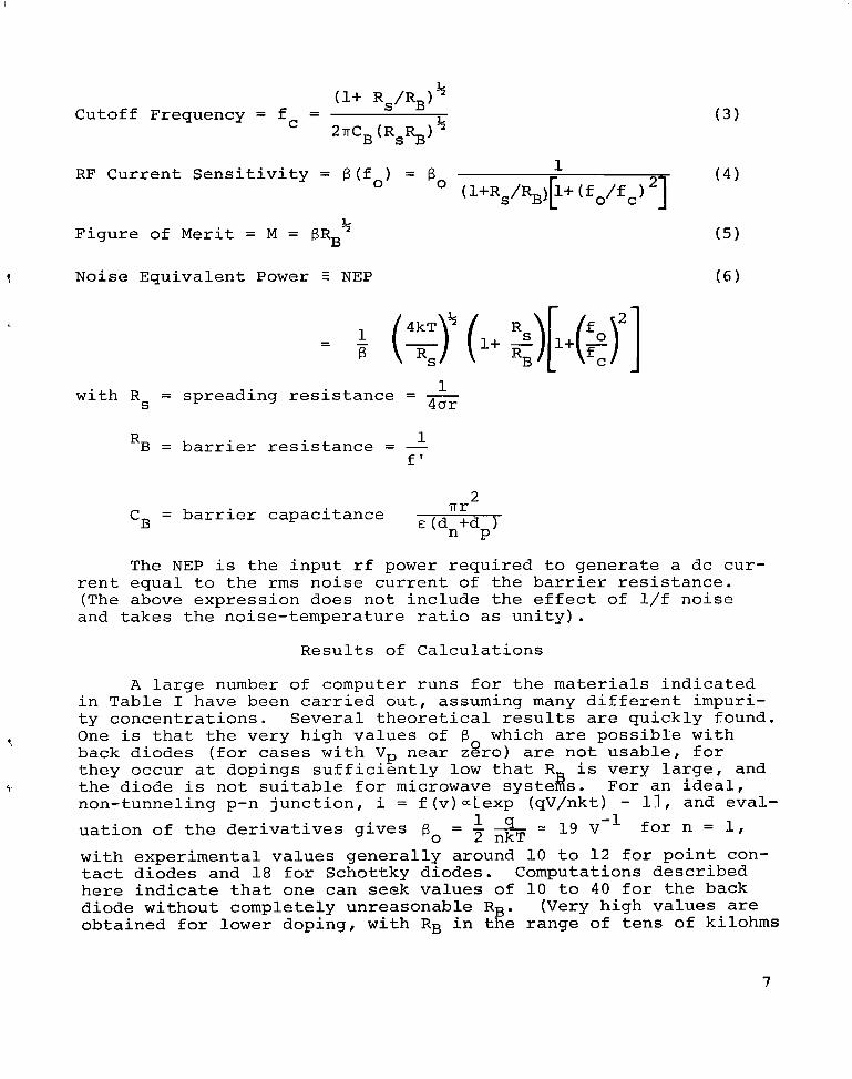
(1+ Rs/RB) % -Cutoff Frequency = fc 2nCB (RsRB) % ( 3 )
1
RF Current Sensitivity = B(fo) = 80 (4)
Figure of Merit = M = f3RB+ t Noise Equivalent Power E NEP
I
1with Rs = spreading resistance = ~ 4ar
RB = barrier resistance = -1 f'
2nrCB = barrier capacitance E (dn+dP)
The NEP is the input rf power required to generate a dc current equal to the rms noise current of the barrier resistance. (The above expression does not include the effect of l/f noise and takes the noise-temperature ratio as unity).
Results of Calculations
A large number of computer runs for the materials indicated in Table I have been carried out, assuming many different impurity concentrations. Several theoretical results are quickly found.
', One is that the very high values of f3 which are possible with back diodes (for cases with Vp near z&o) are not usable, for they occur at dopings sufficiently low that R is very large, and
't the diode is not suitable for microwave systeib. For an ideal,non-tunneling p-n junction, i = f(v)aCexp (qV/nkt) - 11, and evaluation of the derivatives gives f3 o = 1%2 nkT = 19 V-l for n = 1, with experimental values generally around 10 to 12 for point contact diodes and 18 for Schottky diodes. Computations described here indicate that one can seek values of 10 to 40 for the back diode without completely unreasonable RB. (Very high values are obtained for lower doping, with RB in the range of tens of kilohms
7
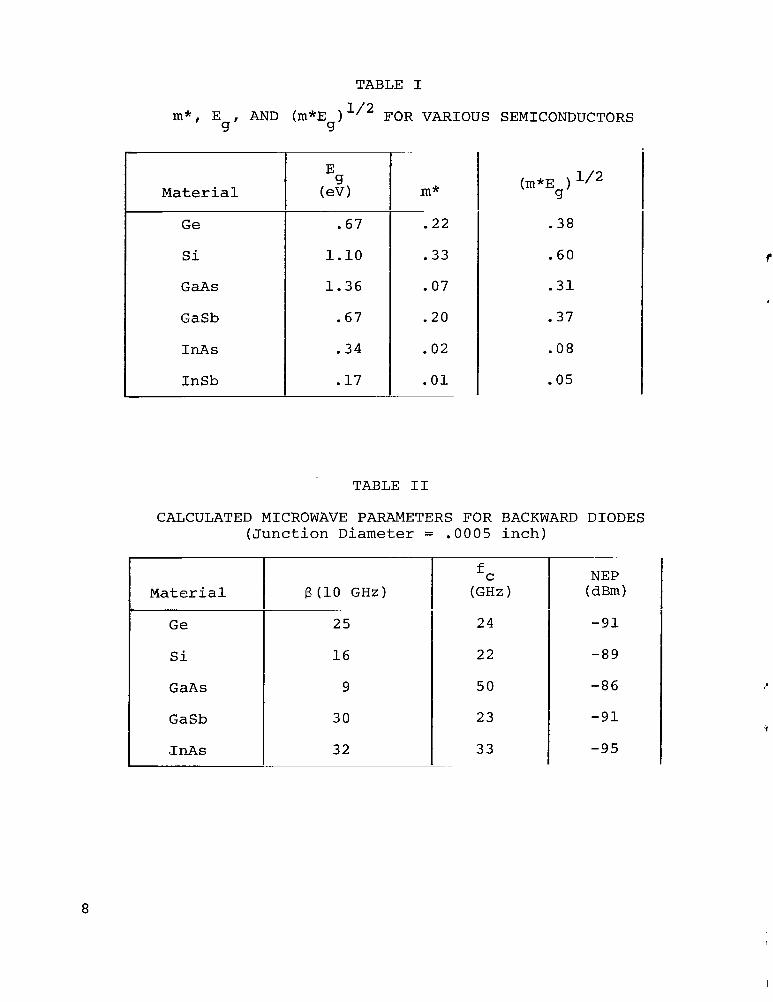
TABLE I
m*, E , AND (m*E ) FOR VARIOUS SEMICONDUCTORS g g
Material m*
Ge .67 - 2 2 .38
Si 1.10 .33 .60
GaAs 1.36 .07 . 3 1
GaSb .67 .20 .37
InAs . 34 . 0 8
InSb .17 .01 .05
TABLE I1
CALCULATED MICROWAVE PARAMETERS FOR BACKWARD DIODES (Junction Diameter = .0005 inch)
NEP Material B ( l 0 GHz) (dBm)
~~
Ge 25 24 - 9 1
Si 1 6 22 -89
GaAs 9 5 0 -86
GaSb 30 23 - 9 1
.InAs 32 3 3 -95
8
I
c

24
2 Ge 25pM1 , I I l l l l l r l l I l r ~ l I r I I I I
3 200 400 600 800 1000 1200 1400 1600 1800 2000 2200
Re- (OHMS)
Figure 2.- Current sensitivity f3 vs. barrier resistance RB for various materials and junction diameters
- (10 G H z ) 12
T I I > Y IO
ht 9 I n A s 4 P M
Y5:8
a 1 7
6
5
4
3
2 I n A s 10/1 M
I G e 4 p M . . . . .
0 200 400 600 800 1000 1200 1400 1600 I800 2000
Re- (OHMS)
Figure 3 . - Current sensitivity f3 vs. barrier resistance RB for various materials and junction diameters (50 GHz
9
I
of
or higher). The peak voltages for such units tend to be in the range of 20 to 40 mV. The most important comparative results are summarized in Table 11, where a junction diameter of .0005 inch is assumed. One finds that the expected advantages of InAs are confirmed. Although GaAs shows a particularly high fc, the Bo (10 GHz) is quite low, and offers no improvement. Not surprisingly, GaSb is seen as approximately equal to Ge. However, the vastly greater technological effort which has gone into germanium makes it not surprising that commercial microwave back diodes are germanium. It should be noted that the advantage of InAs is as much in B as in fc, which is not so markedly improved as might have been expected. This results from the relatively tlow doping at which tunneling occurs, so that optimum microwave detection parameters are found for somewhat higher RB than is the case for other materials. This diminishes the benefit of the >
decrease of CB, but the moderate increase in RB can be helpfulfor system applications. The 4 dB improvement in NEP is a significant gain in sensitivity.
A more detailed analytical comparison of InAs and Ge diodes shows their differences in several ways, and suggests the kinds of compromises involved in optimization. Figures 2 and 3 show theoretical current sensitivity 6, at 10 and 50 GHz, as a function of barrier resistance. Of course, the true independentvariable here is impurity concentration, but resistance for a junction of specified area is an equally valid parameter and more easily related to experimental efforts and device applications.The most important conclusion to be drawn from both sets of curves is that InAs diodes can have substantially larger junction area than Ge detectors of equivalent sensitivity. The alternative viewpoint, that InAs can provide greater sensitivity for the same size, is equally valid, although the improvement is likely to be small enough so that the reliability advantages of largejunctions (high burnout energies and reduced fragility) will take precedence. Note that for 25-1-(junctions (approx. 0 . 0 0 1 inch)the maximum in B occurs at relatively high doping, and, therefore, at low RB. These RB values are rather difficult to use in a microwave system, so that a junction diameter not much larger than 101-1 is important for good performance. There are two dominant factors determining the B vs RB curves. One is change of the curvature of the current-voltage characteristic as doping is varied, so that Bo decreases with increasing impurity concentration. The >
other major variable is the cutoff frequency fc, which decreases with increasing RB. These effects interact in a way which is sensitive to junction area. A change in area requires different doping, with different tunnel current density, to give the same RB, though Bo will change. In addition, the cutoff frequency depends
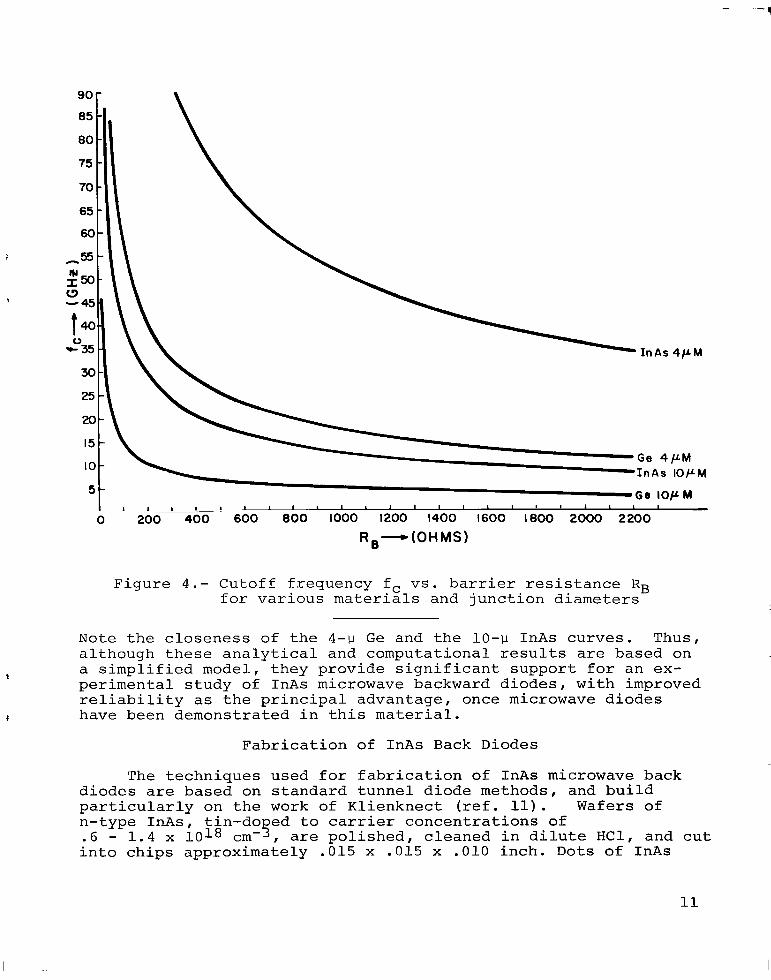
, the barrier capacitance, and the spreading resistance, all On w ich are functions of area. Figure 4 shows fc plotted againstRB for several relevant cases, and the advantage of InAs in this area is apparent.
10
- ~~~~~
90 85 80
-75
70 -65
60
--55
%Q-W -45 f
fa2 3 5 30
25
20
-15 Ge 4 p M
IO - I n A s IOpM 5 - Go I O P M
I ~ " l I ! ~ " " ' " ~ ~ ~ " 0 200 400 600 800 1000 1200 1400 1600 I800 2000 2200
R,-(OHMS)
Figure 4.- Cutoff frequency fc vs. barrier resistance RB for various materials and junction diameters
Note the closeness of the 4-11 Ge and the 10-1-1 InAs curves. Thus, although these analytical and computational results are based on a simplified model, they provide significant support for an ex
1 perimental study of InAs microwave backward diodes, with improvedreliability as the principal advantage, once microwave diodes
4 have been demonstrated in this material.
Fabrication of InAs Back Diodes
The techniques used for fabrication of InAs microwave back diodes are based on standard tunnel diode methods, and build particularly on the work of Klienknect (ref. 11). Wafers of n-type InAs, tin-do ed to carrier concentrations of .6 - 1.4 x lo1* cm-5, are polished, cleaned in dilute H C 1 , and cut into chips approximately .015 x .015 x .010 inch. Dots of InAs
11
containing 10 percent cadmiun, with diameters from .002 to .005 inch, are then alloyed into the chips in a hydrogen atmosphere at a temperature of 4500 to 500OC which is held for 30 sec. to 1 min:, followed by fairly fast cooling (5 to 100C/sec). The chip is then mounted in a standard varactor package using 60/40lead-tin solder at 3000, and a .001 inch gold wire is welded across the top of the package and pushed down into contact with the dot. The assembly is then heated to 275O (in hydrogenatmosphere), fusing the wire to the dot.
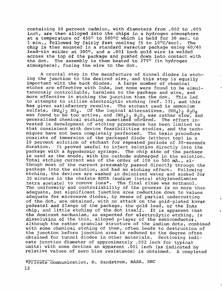
A crucial step in the manufacture of tunnel diodes is etch- I, ing the junction to the desired size, and this step is equallyimportant with the back diodes. A large number of chemical etches are effective with InAs, but none were found to be simul- I
taneously controllable, harmless to the package and wire, and more effective in etching the junction than the dot. This led to attempts to utilize electrolytic etching (ref. 13), and this has given satisfactory results. The etchant used is ammonium sulfate, (NH4)2 SO4. Of the logical alternatives, (NH4)2 S 2 0 8 was found to be too active, and (NH4)2 S203 was rather slow, and generalized chemical etching sometimes occured. The effort invested in development of etching procedures has been limited to that consistent with device feasibilities studies, and the techniques have not been completely perfected. The basic procedureconsists of immersion of the packaged diode (without top) in a 10 percent solution of etchant for repeated periods of 30-seconds duration. It proved useful to inject solution directly into the package with a hypodermic syringe. The chip side of the packageis used as the anode, with the cathode submerged in the solution. Total etching current was of the order of 100 to 500 mA., although most of the current presumably passed directly through the package into the solution, and had no etching effect. Followingetching, the devices are washed in deionized water and soaked for 30 minutes in the chelate EDTA (sodium (tetra) ethylenediamine tetra acetate) to remove ions*. The final rinse was methanol. The uniformity and controllability of the process is no more than adequate, but significant junction area reduction down to values adequate for microwave diodes, by means of partial undercutting U
of the dot, are obtained, with no attack on the gold-plated kovar pedestal and flange of the package, the gold lead, or the InAs chip, and little etching of the dot itself. It is apparent that 4 the dominant mechanism, as expected for electrolytic etching, is dissolution of the thin, alloyed p-layer of the semiconductor, although the rather granular structure of the indium dots, combined with some chemical etching of them, often leads to destruction of the junction before junction area is reduced to the degree often obtained for tunnel diodes in other materials. Sectioning indicate junction diameter of approximately .002 inch for typicalunits; with some devices an apparent .001 inch (as indicated byrelative values of zero bias resistance) is obtained. A completed
*Private communication, D. Sandstrom, NASA, ERC 12
---
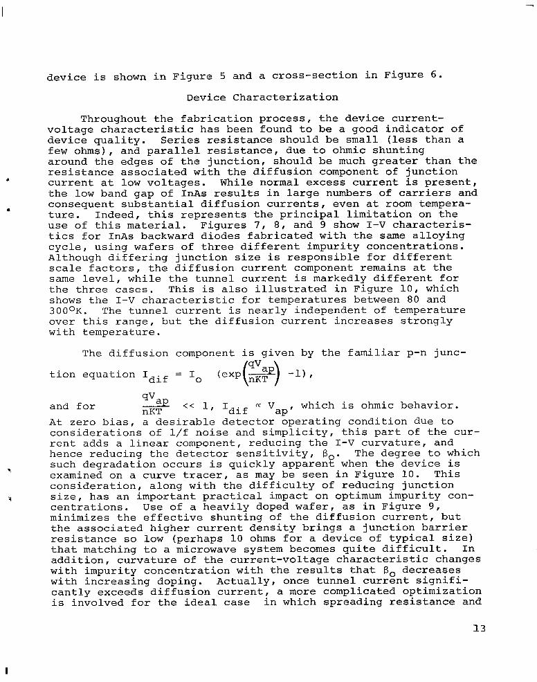
device is shown in Figure 5 and a cross-section in Figure 6 .
Device Characterization
Throughout the fabrication process, the device current-voltage characteristic has been found to be a good indicator of device quality. Series resistance should be small (less than a few ohms), and parallel resistance, due to ohmic shuntingaround the edges of the junction, should be much greater than the resistance associated with the diffusion component of junction* current at low voltages. While normal excess current is present,the low band gap of InAs results in large numbers of carriers and
* consequent substantial diffusion currents, even at room temperature. Indeed, this represents the principal limitation on the use of this material. Figures 7, 8 , and 9 show I-V characteristics for InAs backward diodes fabricated with the same alloyingcycle, using wafers of three different impurity concentrations. Although differing junction size is responsible for different scale factors, the diffusion current component remains at the same level, while the tunnel current is markedly different for the three cases. This is also illustrated in Figure 10, which shows the I-V characteristic for temperatures between 80 and 300°K. The tunnel current is nearly independent of temperature over this range, but the diffusion current increases stronglywith temperature.
The diffusion component is given by the familiar p-n junc
qvand for 3 << 1, Idif a vaP which is ohmic behavior.nKT At zero bias, a desirable detector operating condition due to considerations of l/f noise and simplicity, this part of the current adds a linear component, reducing the I-V curvature, and hence reducing the detector sensitivity, 8,. The degree to which
* such degradation occurs is quickly apparent when the device is examined on a curve tracer, as may be seen in Figure 10. This consideration, along with the difficulty of reducing junctionsize, has an important practical impact on optimum impurity concentrations. Use of a heavily doped wafer, as in Figure 9 , minimizes the effective shunting of the diffusion current, but the associated higher current density brings a junction barrier resistance so low (perhaps 10 ohms for a device of typical size)that matching to a microwave system becomes quite difficult. In addition, curvature of the current-voltage characteristic changeswith impurity concentration with the results that Bo decreases with increasing doping. Actually, once tunnel current significantly exceeds diffusion current, a more complicated optimizationis involved for the ideal case in which spreading resistance and
13
I
3
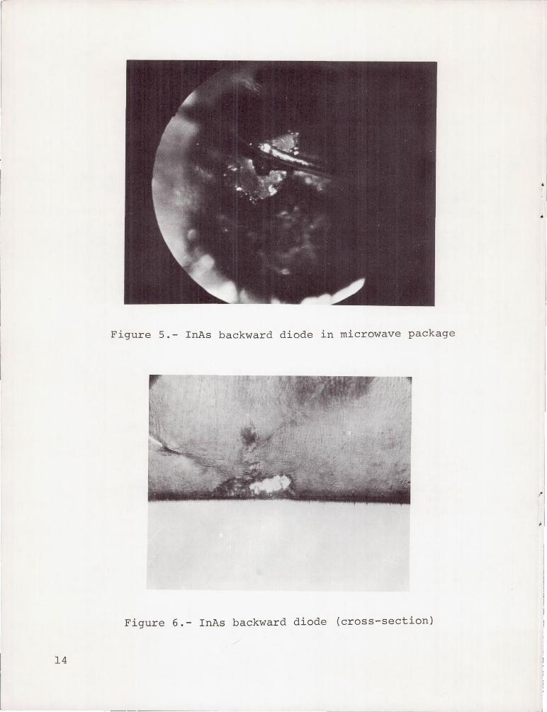
Figure 5.- InAs backward diode in microwave package
.1
Figure 6.- InAs backward diode (cross-section)
l4

Figure 7.- Current-voltagecharacteristic of InAs backward diode. (Carrier concentration .75 x 1 0 1 8 cm-3. Vert.: 5 mA/div. Horiz.: 50 mV./div.)
Figure 9.- Current-voltagecharacteristic of InAs backward diode. (Carrier concentration 3 . 8 x 1018 cm-3. Vert.: .5 mA/div. Horiz.: 50 mV./div.)
I .-
I
Figure 8.- Current-voltagecharacteristic of InAs backward diode. (Carrier concentration 1.6 x 1 0 1 8 cm-3. Vert,: 5 mA/div. Horiz.: 50 mV./Div.)
Figure 10.- Current-voltagecharacteristic of InAs backward diode for various temperaturesfrom 80° K to 300° K. (Forward current increases with temperature.)
15

cut-off frequency must be considered. This has been examined by means of the computer calculations described earlier. For a given minimum junction area, there is generally a particular doping level (and associated peak voltage and peak current) for highest sensitivity at a particular frequency, and the maxima found are generally fairly broad. In the experimental work decribed here, emphasis has been given to verification of basic features of InAs backward diodes, without seeking engineeringperfection. For most materials, including InAs, the optimum case includes peak voltage of approximately 20 to 40 mV, and that is the range in which our diodes fall. Microwave performance of these diodes has varied considerably, in a manner generally qualitatively predictable from the shape of the I-V curve and the apparent junction size (as estimated from the zero bias resistance). The best diodes have exhibited tangential sensitivity(TSS) essentially equivalent (+ 1 dB) to a number of commercial microwave backward diodes. Results at 8.8 GHz, for a video frequency of 100 kHz and bandwidth of 10 kHz are shown in Table 111. Tangential sensitivity represents the input power necessary for the detected signal to be distinguishable from the noise (predominantly thermal) generated in the diode. For the bandwidth used, the TSS values measured are rather lower in magnitude than expected, apparently due to system noise which exceeds the thermal noise of the diodes by perhaps 5 dB. However, the commercial and InAs diodes are of the same impedance level, so the comparison remains valid. Measurements of the open-circuit voltagesensitivity y('vdc/P,f) and 1,2,4, and 9 GHz indicate a cutoff frequency fc of approximately 2 GHz for the better units, althoughthe best diodes (those which gave the competitive TSS measurements) were accidentally destroyed before these measurements could be made. These results are shown in Table IV, along with commonly used figure of merit, M=BR4B = y q .
All diodes were exposed to microwave radiation at a 300-mW power level without degradation. Most of these devices have somewhat larger junction areas than would a perfected microwave diode, so this is not conclusive. But, burnout powers of 100 to 200 mW are typical of published specifications.
Fragility is also difficult to characterize with a limited number of diodes, made by a variety of techniques, with electrical performance the primary consideration. In general, the devices have survived considerable handling, dropping, etc, while on the other hand, the commercial back diodes tested have been quite delicate, and often do not survive repeated handling in the course of measurements. Again, the InAs diodes are rather larger than optimum, so that this result can not be considered definitive. However, it does support the reasonable assertion that for two diodes of comparable detection performance, the devices with larger junctions are significantly more rugged.
16
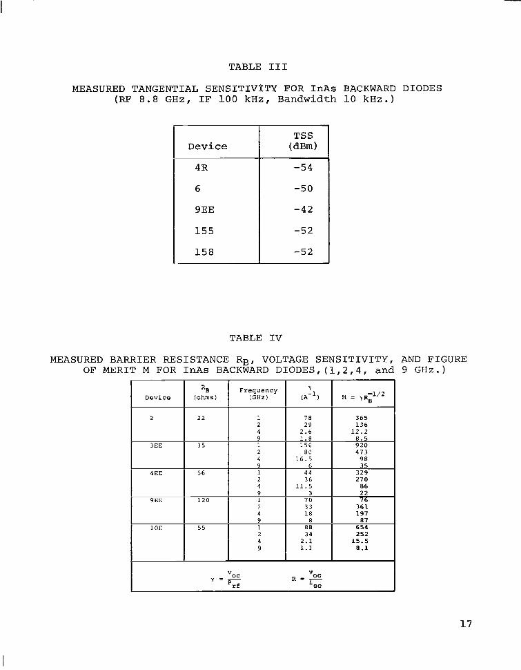
TABLE I11
MEASURED TANGENTIAL SENSITIVITY FOR InAs BACKWARD DIODES (FU? 8.8 G H z , IF 1 0 0 k H z , Bandwidth 1 0 k H z . )
TABLE IV
MEASURED BARRIER RESISTANCE RB, VOLTAGE SENSITIVITY, AND FIGURE OF MERIT M FOR InAs BACKWARD DIODES,(1,2,4, and 9 G H z . )
Y = "oc
p R L -"oc rf ISC
17

CONCLUSION
Analysis and calculations have been carried out supportingthe initial qualitative judgment that microwave backward diodes fabricated from InAs will have significant advantages over currently used materials, particularly in the area of reliability.An experimental program including fabrication and characterization of such diodes has been undertaken. Microwave (9 GHz)diodes of adequate quality have been'constructed,although etching procedures are not as yet sufficiently refined to providejunctions with area as small as desired, particularly on a reproducible basis. This has been a limited fabrication program,appropriate to an exploratory study. However, it has providedconfirmation for the prediction that good microwave back diodes can be produced in InAs, for substantially larger junctions than used in Ge back diodes, with consequent reliability improvements.These results also tend to support the result that improvementin sensitivity at a specified frequency, or in cutoff frequency, can be expected, although improvement in this sphere is less dramatic. The principal weakness of the InAs diodes, resultingfrom the low bandgap, is the limitation in maximum operating temperature. Among the better diodes fabricated, from dopingappropriate to detector applications, diffusion current becomes comparable to tunnel current (with deleterious egfects on performance) for an ambient temperature of 25 to 35 C. While final fabrication refinement might give some improvement, this restriction must be regarded as inherent. This effect could be countered through moderate cooling - possibly thermoelectric - although this approach adds to power consumption and system complexity, and generally can be justified only on the basis of very marked iniprovement in performance. The InAs diode is already attractive for applications where only lower temperatures are to be encountered, as there is little change in its microwave characteristic between 80 and 300°K.
On theoretical grounds, a substantially greater bandgapcould be obtained without seriously compromising the effective mass by use of the ternary compound semiconductor indium arsenidephosphide. Research on this must await availability of goodquality InAs-P with proper doping and As/P ratio, and this singleapplication does not appear to warrant the material developmenteffort that would be necessary.
In summary, an exploratory investigation has indicated that significant improvements in back diodes can be realized throughthe use of new materials. While the semiconductor used here, InAs, is limited to operation at room temperature and.below, the results obtained with it strongly suggest the conclusion that substantially improved detectors for a wider temperature range can be achieved by extension to indium arsenide-phosphide.
18

APPENDIX
CALCULATION OF CHARACTERISTICS OF TUNNELING JUNCTION
The physical model used is that of a conventional p-n junction. Perfect crystal structure is assumed, with an impurityconcentration which changes abruptly from Nd, at energy - Ed (n-region), to Na, at energy Ea (p-region). The band structure i s taken to be particularly simple--parabolic, and isotropic in k. Only direct tunneling transitions are considered. This could be a serious restriction, since both germanium and silicon are indirect-gap materials. However, the principal error will be only in current densities; so, much useful information can be obtained for these materials as well. (Most 111-V semiconductors of current interest are essentially direct-gap and accurate estimates can be obtained for them). In fact, results for Si and Ge do agree well with experimental results of others.
Tunneling current is a very sensitive function of tunnelingdistance, and considerable care is taken in determining this parameter. The various material constants are specified for the temperature assumed and are taken to be independent of appliedvoltage and Fermi levels and constant throughout the materials. The required data for the material includes band gap, dielectric constant, lattice constant, hole and electron mobilities, effective masses, and recombination times. The diffusion constants are calculated from the mobilities using the Einstein relation (D = kTu/q) corrected for degeneracy. The diffusion lengths are determined from the diffusion constants and recombination times. In addition, the impurity doping parameters are specified, including both concentrations and energy levels.
The first step in determining the electrical characteristics of a semiconductor is calculation of the position of the Fermi level. For a p-n diode, this is done separately for the p and n regions.
The basic equation used is that of charge neutrality:
electrons in holes in 3-~onized]+~n-ionizedband donors acceptors 1 = 0 (AI)
The assumption is made that in the n region EJ, = 0, and in the p region Nd = 0.
19
--
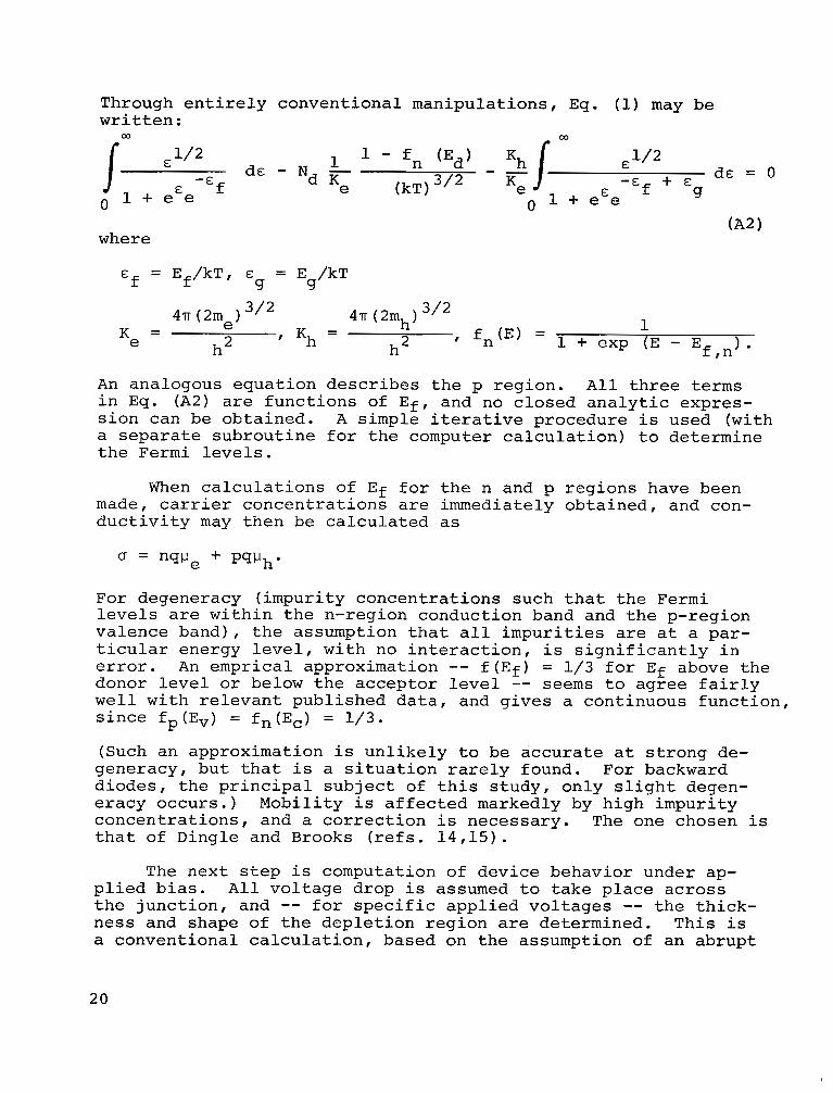
Through entirely conventional manipulations, Eq. (1)may be written:
1de - Nd K n E dE = 0 e g
where (A2 1
= Ef/kT, E g
= E4/kT
An analogous equation describes the p region. A l l three terms in Eq. (A2) are functions of Ef, and no closed analytic expression can be obtained. A simple iterative procedure is used (with a separate subroutine for the computer calculation) to determine the Fermi levels.
When calculations of Ef for the n and p regions have been made, carrier concentrations are immediately obtained, and conductivity may then be calculated as
cT = nqlJe + pqlJh.
For degeneracy (impurity concentrations such that the Fermi levels are within the n-region conduction band and the p-regionvalence band), the assumption that all impurities are at a particular energy level, with no interaction, is significantly in error. An emprical approximation f(Ef) = 1/3 for Ef above the donor level or below the acceptor level -- seems to agree fairlywell with relevant published data, and gives a continuous function, since fp(Ev) = fn(Ec) = 1 / 3 .
(Such an approximation is unlikely to be accurate at strong degeneracy, but that is a situation rarely found. For backward diodes, the principal subject of this study, only slight degeneracy occurs.) Mobility is affected markedly by high impurityconcentrations, and a correction is necessary. The one chosen is that of Dingle and Brooks (refs. 14,151.
The next step is computation of device behavior under applied bias. All voltage drop is assumed to take place across the junction, and -- for specific applied voltages -- the thickness and shape of the depletion region are determined. This is a conventional calculation, based on the assumption of an abrupt
20

’FV
junction. Junction capacitance (per unit area) is then calculated from the depletion layer width and the dielectric constant of the material. For a specified junction area, junction (barrier)capacitance CB is then known, as is the spreading resistance, RS, which is determined from the semiconductor conductivity:RS = 1/4crr, where r is the junction radius.
Tunnel current is calculated from the following conventional equations (ref. 16):
with the tunneling probability Pt written as
(A4
IO is a constant, determined from the condition that (ref. 17)
q3’2 (m*) 2’n I = P 9h2E ’ ( A 5
g
F is the average field across the junction, where the actual tunneling distance (t = tn + tP is somewhat less than the depletion width, and this effect is included. In this manner the tunnel current can be calculated for any applied voltage. In the computer program an iterative approach is used first to calculate the peak current and voltage, and this current compared to the theoretical expression for I [Eq. (A5)] to determine the constant I0 which appears in Eq. (A3)?
21

References
1.
2.
3.
4.
5.
6.
7.
8.
9.
10.
11.
12.
13.
Montgomery, M. D.: The Tunnel Diode as a Highly Sensitive Microwave Detector. Proc. IRE (Corres.), vol. 49, 1961 p. 826.
Chase, P. E., and Chang, K. K. N.: Tunnel Diodes as Millimeter Wave Detectors and Mixers. IRE Trans.-MTT (Corres.) MTT-11, 1963, p. 560.
Arizumi, T., Wada, T., and Maruyama, A . : Tunnel Diode Detectors at Microwave Frequencies. Electronics and Communications in Japan, vol. 48, 1965, p. 21.
MOUW, R. B., and Schumacher, F. M.: Tunnel Diode Detectors. the Microwave Journal, vol. 9, no. 1, Jan. 1966, p. 27.
Gabriel, W. F.: Tunnel Diode Low-Level Detection. IEEE Trans.-MTT, MTT-15, 1967, p. 538.
Eng, S. T.: Low-Noise Properties of Microwave BackgroundDiodes. IRE-Trans.-MTT, MTT-9, 1961, p. 424.
Burrus, C. A. Jr.: Backward Diodes for Low-Level Millimeter-Wave Detection. IEEE Trans.-MTT, MTT-11, 1963, p . 357.
Oxley, T. H.: Backward Diodes as Mixers at Microwave Frequencies. J. Electronics and Control, vol . 17, 1964, p . 1.
Wright, R. O., and Goldman, R. L.: Aluminum Alloy Junction Backward Diodes in Microwave Detection Systems. IEEE International Solid State Circuits Conference Digest, vol. 8, 1965, p. 100.
Bowen, C. E.: Forward with Backward Diodes. Electronic Design, vol. 14, no. 1 0 , April 1966, p. 44.
Kleinknect, H. P.: Indium Arsenide Tunnel Diodes. Solid State Electronics, vol. 2, 1961, p . 133.
Hopkins, J. B.: Characteristics of Tunneling P-N Junctions. NASA TN D-4403, March 1968.
Faust, J. W., Jr.: Etching of the III-V Intermetallic Compounds. Compound Semiconductors, vol. 1, Preparationof III-V Compounds, Willardson, R. K., and Goering, H. L., editors, Reinhold, New York, 1961.
2 2

14. Dingle, R. B.: Scattering of Electrons and Holes by ChargedIons and Acceptors in Semiconductors. Phil. Mag., vol . 46, 1955, p. 831.
15. Brooks, H.: Theory of the Electrical Properties of Germanium and Silicon. Advances in Electronics and Electron Physics.vol. 8, 1955, p. 85.
16. Esaki, L.: New Phenomenon in Narrow Germanium PN Junctions. Phys. Rev., vol. 109, 1958, p. 603.
17. Kane, E.D.: Theory of Tunneling. J. Appl. Phys., vol 32, 1961, p. 83.
NASA-Langley, 1969 -9 c- 7 7 23

NATIONALAERONAUTICS AND SPACEADMINISTRATION WASHINGTON,D. C. 20546
OFFICIAL BUSINESS FIRST CLASS MAIL
POSTAGE A N D FEES PAID NATIONAL AERONAUTICS AND
SPACE ADMINISTRATION
POSTMASTER:
“The aei.oiimticn1 diad spnce cictii,ifies of [he Uiiiterl Strites shnll be co?zdi/cted so as t o coiziribicte . . . t o the expniisiori of hifmmz knoiuledge of phenonzeizn iiz the ntitcosphese nud spnce. The Adi)iicislsntioia .rhnll proisjde for the uidest prmtictlbfe find npproprjlite disset)iinn?ioiz of iuforttiLitioii concerniiig i t s tictii,ities mid t h e sesidts thereof.”
-NATIONALAERONAIJTICSA N D SPACE ACT OF 1955
If Undeliverable (Section 158 Posrnl Manual) Do Not Return
NASA SCIENTIFIC AND TECHNICAL PUBLICATIONS
TECHNICAL REPORTS: Scientific and technical information considered important, complete, and a lasting contribution to existing knowledge.
TECHNICAL NOTES: Information less broad in scope but nevertheless of importance as a contribution to existing knowledge.
TECHNICAL MEMORANDUMS: Information receiving limited distribution because of preliminary data, security classification, or other reasons.
CONTRACTOR REPORTS: Scientific and technical information generated under a NASA contract or grant and considered an important contribution to existing knowledge.
TECHNICAL TRANSLATIONS: Information published in a foreign language considered to merit NASA distribution in English.
SPECIAL PUBLICATIONS: Information derived from or of value to NASA activities. Publications include conference proceedings, monographs, data compilations, handbooks, sourcebooks, and special bibliographies.
TECHNOLOGY UTILIZATION PUBLICATIONS: Information on technology used by NASA that may be of particular interest i n commercial and other non-aerospace applications. Publications include Tech Briefs, l-tchnology UtilizationReports and Notes, and Technology Surveys.
Details on the availability of these publications may be obtained from:
SCIENTIFIC AND TECHNICAL INFORMATION DIVISION
NATIONAL AERONAUTICS AND SPACE ADMINISTRATION Washington, D.C. 20546