experimental realization of matrix converter based ... · experimental realization of matrix...
TRANSCRIPT

Vinod Kumar, Ramesh Chand Bansal, and Raghuveer Raj Joshi 670
Experimental Realization of Matrix Converter Based Induction Motor
Drive under Various Abnormal Voltage Conditions
Vinod Kumar, Ramesh Chand Bansal*, and Raghuveer Raj Joshi
Abstract: While the matrix converter has many advantages that include bi-directional power flow, a size reduction, a long lifetime, and sinusoidal input currents, it is vulnerable to the input voltage disturbances, because it directly exchanges the input voltage to the output voltage. So, in this paper, a critical evaluation of the effect of various abnormal voltage conditions like unbalanced power supply, balanced non-sinusoidal power supply, input voltage sags and short time blackout of power supply on matrix converter fed induction motor drives is presented. The operation under various abnormal conditions has been analyzed. For this, a 230V, 250VA three phase to three phase matrix converter (MC) fed induction motor drive prototype is implemented using DSP based controller and tests have been carried out to evaluate and improve the stability of system under typical abnormal conditions. Digital storage oscilloscope & power quality analyzer are used for experimental observations. Keywords: Harmonics, matrix converter, non-sinusoidal supply, power quality, voltage sag.
1. INTRODUCTION The matrix converter has many advantages that
include bi-directional power flow, a size reduction, a long lifetime, and sinusoidal input currents. Further-more, in connection with this technique, a novel insulated gate bipolar transistor (IGBT) with reverse blocking capability has been developed to improve the efficiency [1]. Thus, the matrix converter has drawn much attention from researchers [2-5]. However, it has some difficulties with practical use. One of them is its vulnerability to the input voltage disturbances (for example, input voltage distortion, input voltage unbalance, and so on).
A Voltage sag [6], or voltage dip, is a reduction of the voltage at a customer position with duration of between one cycle and a few seconds. Motor starting, short circuits and fast reclosing of circuit breakers cause voltage sags. Voltage sags normally do not cause equipment damage, but can easily disrupt the operation of sensitive loads such as electronic adjustable-speed drives [7].
Severe voltage sag can be defined as one that falls
below 85% of rated voltage, termed as 15% sag according to the definition in [6].
Power quality surveys are a common practice and frequently appear in the literature [7-9]. According to these surveys, voltage sags are the main cause of disturbances. For example, in the survey reported in [9], 68% of the disturbances registered were voltage sags, and they were the only cause of production loss. This loss was caused by voltage drops of more than 13% of rated voltage and duration of more than 8.3 ms (1/2 cycle).
Reference [8] states that a little more than 62% of the disturbances recorded were voltage sags with duration of less than 0.5s (30 cycles). In a recent study (17-month period) [7] conducted at two industrial sites with adjustable-speed drives (ASD’s), it was concluded that voltage sags with a duration of 12 cycles or more and lower than 20% voltage drop will trip out the ASD involved in a continuous process. Comparing this data with the “tolerance curve” published in [7] establishes that modern ASD’s appear to be more sensitive than data processing equipment.
In textile and paper mills, brief voltage sag may potentially cause an ASD to introduce speed fluctuations that can damage the end product. Furthermore, a brief voltage sag also causes a momentary decrease in dc-link voltage, triggering an under voltage trip or resulting in an over current trip. Such nuisance tripping of ASD equipment employed in continuous process industries contributes to loss in revenue and can incur other costs.
Till date, much analysis is based on the assumption that the input voltages are well balanced sinusoidal and which results in the ideal output waveform. But it
__________ Manuscript received February 29, 2008; accepted May 28, 2008. Recommended by Guest Editor Seung Ki Sul. Vinod Kumar and Raghuveer Raj Joshi are with the Department of Electrical Engineering, MPUAT, Udaipur 313001, India (e-mails: [email protected], rrjoshi_iitd@ yahoo.com). Ramesh Chand Bansal is with the School of Information Technology & Electrical Engineering, University of Queensland, St. Lucia, Qld-4072, Australia (e-mail: bansal@ itee.uq.edu.au). * Corresponding author.
International Journal of Control, Automation, and Systems, vol. 6, no. 5, pp. 670-676, October 2008

Experimental Realization of Matrix Converter Based Induction Motor Drive under Various Abnormal Voltage …
671
should be noted that harmonics would be always introduced while non-sinusoidal or unbalanced conditions are practically unavoidable. Due to lack of internal energy storage, matrix converter is highly sensitive to the disturbances in the input voltages. Therefore, it’s essential to make harmonic analysis under these conditions. Estimation of harmonics in motor currents is necessary when the input voltages are non-sinusoidal. It enables identifications of the limits on the operating conditions, if any, of the drive. Matrix Converter (MC) has low input current THD characteristics but in some application areas much lower THD level is required [10].
It is known that the supply voltage waveforms may often show typical distortion due to the presence of nonlinear load connected to the grid. Some useful converter harmonic analysis methods under abnormal power supply conditions have been revised here. In [11] a novel analysis method for calculating harmonic components in unbalanced input conditions is proposed. The method gives a clear expression and a better understanding of the converter.
In this paper, a 230V, 250VA three phase to three phase matrix converter fed induction motor drive prototype is implemented which consists of a DSP board using TMS320C671, a FPGA board, an analog board for 4 step commutation and several functional digital logics programmed in Altera EPM7128S, a gate driver and 6 isolated power supply board, a power board containing IGBT matrix module, voltage and current sensors and snubbers. On the basis of experimental tests, the operation of matrix converter under various abnormal voltage conditions has been analyzed. The influence of unbalanced input voltage on input/output performance of MC fed induction motor drive prototype has also been discussed. The accordance of the experimental results with the theoretical investigation validates the credibility of the analysis.
2. ANALYSIS OF MC BASED INDUCTION
MOTOR DRIVE UNDER VARIOUS ABNORMAL VOLTAGE CONDITIONS
The basic structure of the matrix converter is shown
in Fig. 1.
2.1. Operation with balanced power supply Reference [12] has proposed space vector
modulation (SVM) algorithm for matrix converters. It is considered as two steps of input voltage processing. First, the input supply voltages are multiplied with a PWM switching function of the rectifier to yield a dc link. Second, dc link is multiplied by a PWM switching function of inverter to yield the final sine output voltages. The process can be expressed as the following, taking 3×1 matrix converter as an example.
0 o i i 1 0(ω ) [ (ω ] [ (ω ] [ (ω )],TRV t V t T t T t= ⋅ ⋅ (1)
where [Vi (ωit)] is three- phase input voltages, V0 (ω0t) is one phase output ac voltage, [TR (ωit)] is switching function of “rectifier”, [T1 (ω0t)] is switching function of “inverter”.
The input currents are derived by,
i 1 0 0 0[ (ω )] [ (ω )] (ω ),a
Tb R
c
ii T t T t i ti
⎡ ⎤⎢ ⎥ = ⋅ ⋅⎢ ⎥⎢ ⎥⎣ ⎦
(2)
where i0 (ω0t) is the output current. The switching functions for rectifier part can be
written in Fourier series as:
1 2
1 2
1 2
i
1 i i
1 i i
1 i i
[ (ω )]
sin(ω ) sin( ω )
sin(ω 120 ) sin ( ω 120 ) ,
sin(ω 120 ) sin ( ω 120 )
r
nn n n
nn n n
nn n n
T t
A t A n t
A t A n n t
A t A n n t
α
α
α
=
=
=
=
⎡ ⎤⎢ ⎥+⎢ ⎥⎢ ⎥⎢ ⎥
− ° + − °⎢ ⎥⎢ ⎥⎢ ⎥⎢ ⎥+ ° + + °⎢ ⎥⎣ ⎦
∑
∑
∑
L
L
L
(3)
where 1 2
isin ( ω )nn n n
A n n tα
=∑
L
is the high order
harmonics generated pulse with modulation (PWM). Also, the switching function for inverter part can be written in Fourier series as:
1 21 i 1 0 0
,[ (ω ) [ sinω sin( ω )],k
m m mT t B t B k t
α
== + ∑
L
(4)
where 1 2
0,
sin( ω )]km m m
B k tα
=∑
L
is the high order
harmonics generated by PWM. If the input three voltages are balanced and sinusoidal,
A
B
C
S1
iA
iB
iC
a
b
c
ia
ib
ic
S2S3S4S5S6S7S8S9
Fig. 1. Basic structure of matrix converter.
Vinod Kumar, Ramesh Chand Bansal, and Raghuveer Raj Joshi 672
i
sin(ω )
sin(ω 120 ) .
sin(ω 120 )
i
i
i
V t
V V t
V t
α
α
α
+⎡ ⎤⎢ ⎥
= − +⎢ ⎥⎢ ⎥
+ +⎢ ⎥⎣ ⎦
o
o
(5)
Substituting (4) and (5) in (1) and ignoring the high order harmonics yields,
1 10 0
3 cos sin (ω ).2
A B VV tα= (6)
So, it can be concluded that in the balanced conditions, the output voltages and input currents do not contain low order harmonics.
2.2. Operation with unbalanced power supply
For unbalanced sinusoidal power supply, the three-phase unbalanced input voltages can be decomposed into two balanced sets of positive and negative components as (7), [13].
,i p nV V V= + (7)
where
sin(ω )
sin(ω 120 ) ,
sin(ω 120 )
P i
p P i
P i
V t
V V t
V t
α
α
α
+⎡ ⎤⎢ ⎥
= − +⎢ ⎥⎢ ⎥
+ +⎢ ⎥⎣ ⎦
o
o
(8)
sin(ω )
sin(ω 120 ) .
sin(ω 120 )
N i
n N i
N i
V t
V V t
V t
α
α
α
+⎡ ⎤⎢ ⎥
= − +⎢ ⎥⎢ ⎥
+ +⎢ ⎥⎣ ⎦
o
o
(9)
According to (1),
0 0
1 0 1 0
( )[ (ω ] (ω )
[ (ω )] (ω ) [ (ω )] (ω ).
T TP N R i iT Tp R i N R i
V V V T t T t
V T t T t V T t T t
= +
= +
(10) For the positive component, it is the same as in the
balanced condition where no harmonics is generated. For the negative component, it can be derived that,
1
1 10
0 1
[ ( )] ( )3
{sin[2 ) ]4
sin[2 ) ]} ,
TN R i i
ni
i
V T t T tA B V
t t
t M
ω ω
ω ω β
ω ω β
= + +
− − + +
(11)
where M1 is the high harmonic component generated by PWM. So, (11) shows that harmonic components will be introduced by the negative components with the frequency of (2ωi + ω0) and (2ωi - ω0). Thus, it is concluded that unbalance in input supply results in abnormal harmonics in the matrix converter output.
2.3. Operation with balanced non-sinusoidal power supply
The three-phase voltages of balanced non-sinusoidal power supply have the same waveforms but delayed by 2π /3. Similar to the unbalanced condition, the input voltages can be represented as the sum of two parts:
,i I kV V V= + (12)
where Vk is the harmonics with the order of k. Similar to the analysis of unbalanced condition, it can be derived that,
1 0
1 10 0
1 10 0
[ (ω )] (ω )3
{sin[( 1)ω ω ] sin[( 1)ω ω ] }4
where 7, 13, 19......3
{sin[( 1)ω ω ] sin[( 1)ω ω ] }4
where 5, 11, 17......
Tk R i
ki i
ki i
V T t T tAV B
k t k t
kAV B
k t k t
k
=
⎧ − + − − −⎪⎪
=⎪⎨⎪ + + − + −⎪⎪ =⎩
(13) Therefore, it can be concluded that if the input
power supply voltages contains the harmonics with the order of k, the harmonic components with the frequency of (k - 1) ωi ± ω0 and (k + 1) ωi ± ω0 will be introduced in output voltages.
2.4. Operation under input voltage sag and short time
blackout of power supply conditions Voltage sag is a reduction of voltage magnitude with the duration between one cycle and a few seconds, which is usually caused by the fault conditions in the plant or within the utility system. It normally does not cause equipment damage but can disrupt the operation of sensitive loads.
Unlike the voltage source inverter (VSI), a matrix converter has no dc-link capacitor, so power interruption and deep voltage sags will be fatal to the MC fed induction motor drive. During voltage sag event three-phase rectifier is single phased. Since the output power has to be supplied via two phases, this mode increases the rms input current of the drive during the sag event. If the rms input current exceeds the over current protection threshold (usually, 1.2-1.5 p.u.), the drive will trip due to over current. The rms input current of a drive under normal conditions is given by (14).
basebase
LN
VAI
3V= (14)
Now, assuming input VA of the drive is constant during a voltage sag event, we have
Experimental Realization of Matrix Converter Based Induction Motor Drive under Various Abnormal Voltage …
673
baserms,sag
LN
VAI .
3V= (15)
Equation (15) can be expressed in per unit (pu) as
rms,sagrms,sag,pu
base
II .
I= (16)
Substituting (12) and (13) in (14) we get
rms,sag,puI 3.= (17)
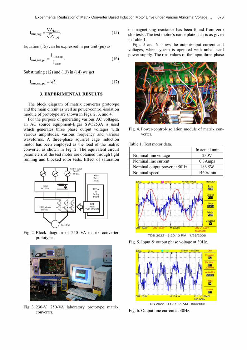
3. EXPERIMENTAL RESULTS The block diagram of matrix converter prototype
and the main circuit as well as power-control-isolation module of prototype are shown in Figs. 2, 3, and 4.
For the purpose of generating various AC voltages, an AC source equipment-Elgar SW5253A is used which generates three phase output voltages with various amplitudes, various frequency and various waveforms. A three-phase squirrel cage induction motor has been employed as the load of the matrix converter as shown in Fig. 2. The equivalent circuit parameters of the test motor are obtained through light running and blocked rotor tests. Effect of saturation
on magnetizing reactance has been found from zero slip tests .The test motor’s name plate data is as given in Table 1.
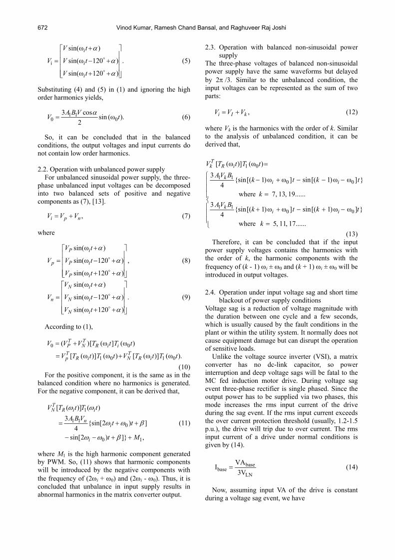
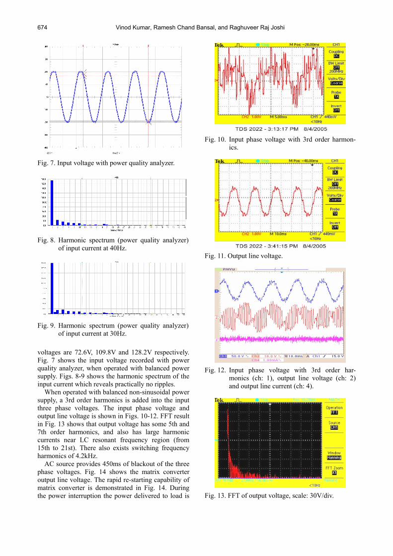
Figs. 5 and 6 shows the output/input current and voltages, when system is operated with unbalanced power supply. The rms values of the input three-phase
Fig. 4. Power-control-isolation module of matrix con-
verter. Table 1. Test motor data. In actual unit
Nominal line voltage 230V Nominal line current 0.8Amps Nominal output power at 50Hz 186.5W Nominal speed 1460r/min
Fig. 5. Input & output phase voltage at 30Hz.
Fig. 6. Output line current at 30Hz.
DSPBased
TMS 320C671
GateDriverBoard
FPGA&
AnalogBoard
Utility Input208 V50 Hz
InputLC Filter
IGBT MatrixModule
Cage I/M Fig. 2. Block diagram of 250 VA matrix converter
prototype.
Fig. 3. 230-V, 250-VA laboratory prototype matrixconverter.
Vinod Kumar, Ramesh Chand Bansal, and Raghuveer Raj Joshi 674
voltages are 72.6V, 109.8V and 128.2V respectively. Fig. 7 shows the input voltage recorded with power quality analyzer, when operated with balanced power supply. Figs. 8-9 shows the harmonic spectrum of the input current which reveals practically no ripples.
When operated with balanced non-sinusoidal power supply, a 3rd order harmonics is added into the input three phase voltages. The input phase voltage and output line voltage is shown in Figs. 10-12. FFT result in Fig. 13 shows that output voltage has some 5th and 7th order harmonics, and also has large harmonic currents near LC resonant frequency region (from 15th to 21st). There also exists switching frequency harmonics of 4.2kHz.
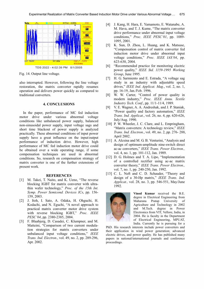
AC source provides 450ms of blackout of the three phase voltages. Fig. 14 shows the matrix converter output line voltage. The rapid re-starting capability of matrix converter is demonstrated in Fig. 14. During the power interruption the power delivered to load is
Fig. 7. Input voltage with power quality analyzer.
Fig. 8. Harmonic spectrum (power quality analyzer)of input current at 40Hz.
Fig. 9. Harmonic spectrum (power quality analyzer)of input current at 30Hz.
Fig. 10. Input phase voltage with 3rd order harmon-
ics.
Fig. 11. Output line voltage.
Fig. 12. Input phase voltage with 3rd order har-
monics (ch: 1), output line voltage (ch: 2) and output line current (ch: 4).
Fig. 13. FFT of output voltage, scale: 30V/div.
Experimental Realization of Matrix Converter Based Induction Motor Drive under Various Abnormal Voltage …
675
also interrupted. However, following the line voltage restoration, the matrix converter rapidly resumes operation and delivers power quickly as compared to traditional converters.
4. CONCLUSIONS
In the paper, performance of MC fed induction
motor drive under various abnormal voltage conditions like unbalanced power supply, balanced non-sinusoidal power supply, input voltage sags and short time blackout of power supply is analyzed practically. These abnormal conditions of input power supply have a great influence on the input/output performance of induction drive. However, high performance of MC fed induction motor drive could be obtained over a wide operating range, if some compensation techniques are used in abnormal conditions. So, research on compensation strategy of matrix converter is one of the further extensions of present work.
REFERENCES
[1] M. Takei, T. Naito, and K. Ueno, “The reverse blocking IGBT for matrix converter with ultra-thin wafer technology,” Proc. of the 15th Int. Symp. Power Semicond. Devices ICs, pp. 156-159, 2003.
[2] J. Itoh, I. Sato, A. Odaka, H. Ohguchi, H. Kodachi, and N. Eguchi, “A novel approach to practical matrix converter motor drive system with reverse blocking IGBT,” Proc. IEEE PESC’04, pp. 2380-2385, 2004.
[3] F. Blaabjerg, D. Casadei, C. Klumpner, and M. Matteini, “Comparison of two current modula-tion strategies for matrix converters under unbalanced input voltage conditions,” IEEE Trans. Ind. Electron., vol. 49, no. 2, pp. 289-296, Apr. 2002.
[4] J. Kang, H. Hara, E. Yamamoto, E. Watanabe, A. M. Hava, and T. J. Kume, “The matrix converter drive performance under abnormal input voltage conditions,” Proc. IEEE PESC’01, pp. 1089-1095, 2001.
[5] K. Sun, D. Zhou, L. Huang, and K. Matsuse, “Compensation control of matrix converter fed induction motor drive under abnormal input voltage conditions,” Proc. IEEE IAS’04, pp. 623-630, 2004.
[6] “Recommended practice for monitoring electric power quality,” IEEE Std. 1159-1995 Working Group, June 1995.
[7] H. G. Sarmiento and E. Estrada, “A voltage sag study in an industry with adjustable speed drives,” IEEE Ind. Applicat. Mag., vol. 2, no. 1, pp. 16-19, Jan./Feb. 1996.
[8] W. W. Carter, “Control of power quality in modern industry,” Proc. IEEE Annu. Textile Industry Tech. Conf., pp. 11/1-11/4, 1989.
[9] V. E. Wagner, A. A. Andreshak, and J. P. Staniak, “Power quality and factory automation,” IEEE Trans. Ind. Applicat., vol. 26, no. 4, pp. 620-626, July/Aug. 1990.
[10] P. W. Wheeler, J. C. Clare, and L. Empringham, “Matrix converters: A technology review,” IEEE Trans. Ind. Electron., vol. 49, no. 2, pp. 276- 288, April 2002.
[11] A. Alcsina and M. G. B. Venturini, “Analysis and design of optimum-amplitude nine-switch direct ac-ac converters,” IEEE Trans. Power Electron., vol. 4, no. 1, pp. 101-112, Jan. 1989.
[12] D. G. Holmes and T. A. Lipo, “Implementation of a controlled rectifier using ac-ac matrix converter theory,” IEEE Trans. Power Electron., vol. 7, no. 1, pp. 240-250, Jan. 1992.
[13] C. L. Neft and C. D. Schauder, “Theory and design of a 30-Hp matrix,” IEEE Trans. Ind. Applicat., vol. 28, no. 3, pp. 546-551, May/June 1992.
Vinod Kumar received the B.E. degree in Electrical Engineering from Maharana Pratap University of Agriculture and Technology in 2002 and M.Tech. degree in Power Electronics from VIT, Vellore, India, in 2004. He is faculty in the Department of Electrical Engineering, MPUAT, India. Currently he is pursuing for a
PhD. His research interests include power converters and their application in wind power generation; advanced electric drives, and power quality. He has published many papers in national/international journals and conference proceedings.
Fig. 14. Output line voltage.

Vinod Kumar, Ramesh Chand Bansal, and Raghuveer Raj Joshi 676
Ramesh Chand Bansal received the M.E. degree from Delhi College of Engineering, Delhi, India, in 1996, MBA degree from Indira Gandhi National Open University, New Delhi, India, in 1997, and the Ph.D. degree from Indian Institute of Technology ((IIT), Delhi, India in 2003. Currently, he is a Faculty in School of Informa-
tion Technology & Electrical Engineering, University of Queensland, St. Lucia, Australia. Earlier he was a Faculty in the Electrical and Electronics Engineering Division, School of Engineering and Physics in The University of the South Pacific, Suva, Fiji during February 2006-June 2008 and Assistant Professor in the Department of Electrical and Electronics Engineering, Birla Institute of Technology and Science, Pilani during June 99-December 2005. He also worked 9 years in Civil Construction Wing, All India Radio. Dr. Bansal is an Editor of IEEE Transactions of Energy Conversion and Power Engineering Letters, Editorial Board Member Institution of Engineering and Technology (IET) - Renewable Power Generation, Electric Components and Power Systems, and Energy Sources, Part B. He is a Senior Member, IEEE, Member of the Institution of Engineers (India), and a Life Member of Indian Society of Technical Education. He is a Member of Board of Directors, International Energy Foundation (IEF), Alberta, Canada. He has published more than 80 papers in national/international journals and conference proceedings. His research interests include reactive power control in renewable energy systems and conventional power systems, power system optimization, analysis of induction generators, and artificial intelligence techniques applications in power systems.
Raghuveer Raj Joshi received bachelor degree in Electrical Engineer-ing from MBM Engineering College, Jodhpur, India, M.Tech. degree from IIT, Delhi, and the Ph.D. degree from RGPV University, Bhopal, India. He is a Faculty in the Department of Electrical Engineering, MPUAT, India. His research interest includes advanced
power electronic converters, and electrical drives. He has published more than 35 research papers in refereed journals and conferences.