experimental assessment of derating guidelines applied to ... · experimental assessment of...
TRANSCRIPT

Journal of Applied Research and Technology 103
Experimental Assessment of Derating Guidelines Applied to Power Electronics Converters S. E. De León-Aldaco*1, J. H. Calleja-Gjumlich2, H. R. Jiménez-Grajales3, F. I. Chan-Puc4
1,2 Departamento de Ingeniería Electrónica
Centro Nacional de Investigación y Desarrollo Tecnológico Cuernavaca, Mor., México *[email protected] 3 Gerencia de Energías no Convencionales Instituto de Investigaciones Eléctricas Cuernavaca, Mor., México 4 División de Ciencias e Ingeniería Universidad de Quintana Roo Chetumal, Q. Roo., México ABSTRACT Power transistors are the most vulnerable components in switching converters, and derating is usually applied to increase their reliability. In this paper, the effectiveness of derating guidelines is experimentally assessed using a push-pull DC-DC converter as a case study, operating in three different environments. After measuring the electrical variables and temperature, reliability was predicted following the guidelines in MIL HDBK 217F. The sensitivity analysis performed indicates that temperature has the largest impact on reliability, followed by environment and device quality. The results obtained demonstrate that a derating procedure based solely on DC ratings does not ensure an adequate performance. Therefore, additional guidelines are suggested to help increase the overall reliability obtained from a power circuit. Keywords: reliability, derating, power converters. RESUMEN En convertidores conmutados, los transistores de potencia son los componentes más vulnerables; para mejorar su confiabilidad es común el empleo de técnicas de sobre-dimensionamiento. En este artículo, la efectividad del sobredimensionamiento se valora de manera experimental, utilizando un convertidor CD-CD tipo push-pull como caso de estudio, operando en tres ambientes diferentes. La confiabilidad se predijo siguiendo el procedimiento en el MIL HDBK 217F, utilizando las mediciones de las variables eléctricas y temperatura. El análisis de sensitividad indica que la temperatura tiene el mayor impacto en la confiabilidad, seguido por el ambiente y la calidad de los dispositivos. Los resultados demuestran que un proceso de sobredimensionamiento basado únicamente en las especificaciones de CD no garantiza un comportamiento adecuado. Se proponen lineamientos adicionales para aumentar la confiabilidad de los circuitos de potencia.
1. Introduction Reliability is usually defined as the ability of an item to perform a required function under stated conditions for a stated period of time [1]. It is widely recognized that any competitive industry must know the reliability of their products, has to be able to control it, and should produce at the optimum reliability level that yields the minimum life-cycle cost to the user [2]. However, this is not always the case. Recently, an industry-based survey aimed at determining the expectations and requirements of power electronics converters was
conducted. The results confirm that reliability is indeed an area of concern and that better monitoring methods and indicators are needed [3]. The desired reliability level must be established at the design phase, because subsequent testing and production will not raise the reliability without a basic design change [4]. Thus, the first step is to select the configuration best suited to the task. It is not easy to identify the most reliable converter in a particular application, but several comparisons that

Experimental Assessment of Derating Guidelines Applied to Power Electronics Converters, S. E. De León‐Aldaco et al. / 103‐114
Vol. 11, February 2013 104
might help for this purpose have been reported in recent years: comparison of three circuits aimed at grid-connected applications [5], of four rectifier-inverter topologies and one matrix converter [6], of a standard three-phase inverter and two redundant configurations [7], of two converters aimed at fuel-cell applications [8], and the comparison of two multilevel converters aimed at motor drive applications [9], among others.
In any configuration, reliability depends heavily on the judicious selection of the individual components involved, and the most failure-prone ones must be carefully specified. Reliability is often expressed either in terms of the failure rate , or the mean time between failures MTBF. Table 1 lists the percent contributions of the components in several power converters to the overall failure rate. The components are broadly grouped in four categories: diodes, transistors (either MOSFETs or IGBTs), capacitors (regardless of the dielectric material), and magnetic elements, including inductors and transformers. According to Table 1,
almost 69% of the failure rate can be attributed to the power transistors. In the opposite side, the contribution of the magnetic elements is quite small. If reliability is to be improved, the weakest component should be upgraded first. A common approach is to derate the components (that is the intentional reduction of electrical, thermal and mechanical stresses on components to levels well below their specified rating) and several guidelines have been provided for critical applications [14]. It is usually assumed that derating provides lower failure rates, but the true effectiveness of the margins cannot be assessed unless the resulting reliability is calculated in the actual application. This paper is aimed at experimentally assessing the effectiveness of derating the switching devices in a power circuit. A push-pull DC-DC converter rated at 100 W was selected for the analysis. Four prototypes were built according to a common design, but using transistors with different ratings. Electrical variables and circuit temperatures were measured at full load.
Ref Application Contribution to overall failure rate (%)
Diodes Transistors Capacitors Magnetic elements
[10]
Wound rotor induction generator
53.38 46.62 N.A. N.A.
Permanent magnet generator
34.57 65.43 N.A. N.A.
[11]
Boost converter 2.91 75.70 20.85 0.54
Forward converter 32.65 54.20 12.30 0.86
Single-phase PFC 12.19 76.52 10.17 1.12
[12]
Boost converter, CCM, 1 kW
5.08 67.36 24.46 3.10
Boost converter, DCM, 1 kW
3.75 76.74 17.42 2.09
Boost converter, CCM, 300 W
4.89 67.43 24.14 3.54
Boost converter, DCM, 300 W
3.51 74.44 19.60 2.45
[13] Automotive inverter 2.79 88.00 9.21 N.A.
Average: 15.57 69.24 17.26 1.96
Table 1. Percent failure rates for components in power electronics converters.

Experimental Assessment of Derating Guidelines Applied to Power Electronics Converters, S. E. De León‐Aldaco et al. / 103‐114
Journal of Applied Research and Technology 105
Afterwards, the resulting reliabilities were calculated following the procedure in the military handbook MIL HDBK 217F (MH217), taking into account three operating environments [15]. The sensitivity analysis indicates that temperature has the largest impact on reliability, followed by environment and device quality. The results obtained demonstrate that a derating procedure based solely on DC ratings does not ensure an adequate performance. After analyzing the experimental results, several guidelines are suggested to help increase the overall reliability obtained from a power circuit. 2. Reliability prediction
Let xi be the state of component i, such that xi = 0 if the component has failed, and xi = 1 if the component is functioning. Let XS be the state of a system comprised by n individual components. In a serial system (from a reliability point of view):
n
i
iS xX1 (1)
that is, the system will fail if any of the components fails. In a parallel (or redundant) system:
n
i
iS xX1
11 (2) thus, the system remains functional when at least one of its components functions does too. Power electronics converters have become a commodity, and redundancy is seldom used. Competitive advantages are obtained from better performance, and longer operational lives [16][ 17]. Such is the case of most converters in PV application, which are of the series type. The reliability of any type of item is a function of
the item’s failure rate which, for any electronic component, is assumed to be constant. The reliability R(t) is then
)texp()t(R (3) Photovoltaic converters are expected to operate continuously for as long as possible, and a specific lifetime does not exist. Therefore, mission reliability is not the best way to specify reliability requirements. A more useful parameter for continuously operating items is the mean time between failures MTBF, given by
1)(
0
t
dttRMTBF (4)
or, for a system comprised by n individual components:
n
i
i
MTBF
1
1
(5)
If the failure rate for a power converter is to be predicted using (5), then the individual failure rates for all the components in the converter must be computed first. Failure rates can be predicted from observed laboratory or field data, according to statistical analysis methods. One possible source of data is the MH217, which contains information for all types of components operating under prescribed conditions, obtained by collecting data since the late 50s. According to the model in MH217, the failure rate P for any given part can be computed as:
jbP (6)
where b is the base failure rate under the prescribed conditions, and tabulated in the handbook. The j terms are stress factors that take into account the severity of the particular operational conditions. Those applying to the components usually employed in a power electronics converter are listed in Table 2.

Experimental Assessment of Derating Guidelines Applied to Power Electronics Converters, S. E. De León‐Aldaco et al. / 103‐114
Vol. 11, February 2013 106
The temperature factor T is based on the Arrhenius equation as follows: = − (7)
The correspondences to TX and the activation energy Ea values are listed in Table 3. The term kB = 8.617 x 10⁻⁵ eV/°K corresponds to the Boltzmann's constant.
Component Ea (eV) TX (°C)
(Temperature at) Power Transistor 0.166 Junction TJ Diode 0.266 Junction TJ Capacitor 0.15 Ambient TA
Inductor 0.11 Hot spot THS
Transformer 0.11 Hot spot THS Snubber resistor 0.08 Component TR
Table 3. Variables for the calculation of T.
The junction temperature TJ, in °C, can be calculated using: = + (8) where TCASE is the case temperature, Pd corresponds to the power dissipated at the device, and JC is the thermal resistance from junction to case. The hot-spot temperature THS for magnetic components can be calculated using: = + 1.1 ∆ (9)
where TA is the ambient temperature. T is the average temperature rise above TA, and can be approximated using: ∆ = (10)
where Pd corresponds to the power dissipated (W) and A is the radiating surface area of the component’s case (in2).
The environment stress factor E ranges from ground benign to cannon launching. The evaluations reported herein include ground benign GB (non-mobile, temperature and humidity controlled environments), ground fixed GF (moderately controlled environments with adequate cooling air), and ground mobile GM (equipment installed on wheeled vehicles).
The quality factor Q depends on the package (plastic, JAN qualified, and so forth). The factor πA
is the application factor for transistors, set according to the type of use of the transistor in the circuit (mainly the power rating, Pr). The capacitance factor πC is determined by = . (11) The voltage stress factor πV for the capacitor, is defined by
= . + 1 (12) where S is the ratio of operating voltage to rated voltage. The electrical stress factor πS for diodes is defined by = 0.054 for VS <0.3 (13)
= . for 0.3 < VS ≤ 1 (14) Where VS is the ratio between the reverse voltage applied to the diode, and the corresponding rating. In resistors, πS is the power stress factor defined by = 0.71 . (15)
Component πT πQ πE πA πC πV πS πP MOSFET
Resistor
Transformer Diode
Capacitor Inductor
Table 2. Stress factors
Experimental Assessment of Derating Guidelines Applied to Power Electronics Converters, S. E. De León‐Aldaco et al. / 103‐114
Journal of Applied Research and Technology 107
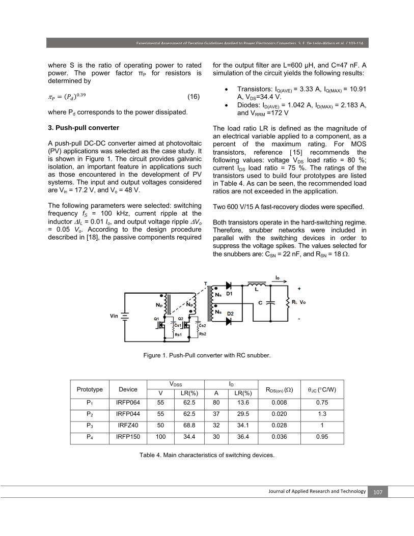
where S is the ratio of operating power to rated power. The power factor πP for resistors is determined by = . (16) where Pd corresponds to the power dissipated. 3. Push-pull converter A push-pull DC-DC converter aimed at photovoltaic (PV) applications was selected as the case study. It is shown in Figure 1. The circuit provides galvanic isolation, an important feature in applications such as those encountered in the development of PV systems. The input and output voltages considered are Vin = 17.2 V, and Vo = 48 V. The following parameters were selected: switching frequency fS = 100 kHz, current ripple at the inductor IL = 0.01 Io, and output voltage ripple Vo = 0.05 Vo. According to the design procedure described in [18], the passive components required
for the output filter are L=600 µH, and C=47 nF. A simulation of the circuit yields the following results:
Transistors: IQ(AVE) = 3.33 A, IQ(MAX) = 10.91 A, VDS=34.4 V.
Diodes: ID(AVE) = 1.042 A, ID(MAX) = 2.183 A, and VRRM =172 V
The load ratio LR is defined as the magnitude of an electrical variable applied to a component, as a percent of the maximum rating. For MOS transistors, reference 15 recommends the following values: voltage VDS load ratio = 80 %; current IDS load ratio = 75 %. The ratings of the transistors used to build four prototypes are listed in Table 4. As can be seen, the recommended load ratios are not exceeded in the application. Two 600 V/15 A fast-recovery diodes were specified. Both transistors operate in the hard-switching regime. Therefore, snubber networks were included in parallel with the switching devices in order to suppress the voltage spikes. The values selected for the snubbers are: CSN = 22 nF, and RSN = 18 .
Figure 1. Push-Pull converter with RC snubber.
Prototype Device VDSS ID
RDS(on) () JC (C/W) V LR(%) A LR(%)
P1 IRFP064 55 62.5 80 13.6 0.008 0.75
P2 IRFP044 55 62.5 37 29.5 0.020 1.3
P3 IRFZ40 50 68.8 32 34.1 0.028 1
P4 IRFP150 100 34.4 30 36.4 0.036 0.95
Table 4. Main characteristics of switching devices.

Experimental Assessment of Derating Guidelines Applied to Power Electronics Converters, S. E. De León‐Aldaco et al. / 103‐114
Vol. 11, February 2013 108
4. Measurements
The tests were performed using as input a DC power supply instead of a PV module, thus providing equal operating conditions for the four prototypes. There were two sets of measurements performed. The first one involved the measurement of electrical variables in all the components. Figure 2 illustrates typical waveforms at the MOSFET transistors. The calculation of T requires the measurement of case temperatures in all the components comprising the converter. Temperatures were measured using a thermographic camera. Figure 3a shows the image of a prototype operating at full load. The transistor heatsinks are discernable at
the top, left and right sides of the image; the hot spot at the bottom corresponds to the power transformer. Figure 3b illustrates the temperature of a diode mounted in a stamped heatsink. 5. Results The stress factors for each component were calculated from maximum voltage and current data, power dissipation and temperature measurements. The procedure briefly described in Section II was implemented as mathematical routines in the Mathcad software package. The calculations were focused exclusively on devices in the power stage and do not include control circuits or drivers. A detailed example of the reliability calculations is included in Appendix A.
Figure 2. Waveforms at a transistor. Top trace: Drain to source voltage, VDS (25 V/div). Bottom trace: Drain current, ID (5 A/div). Time base: 2 μs/div.
(a) (b)
Figure 3. Thermographic images of the power converter. a) Top view. b) Detail of one of the diodes.

Experimental Assessment of Derating Guidelines Applied to Power Electronics Converters, S. E. De León‐Aldaco et al. / 103‐114
Journal of Applied Research and Technology 109
Figure 4 illustrates the failure rates for the components included in prototype P1, operating in a ground fixed environment at an ambient temperature TA = 28 ºC. The percent contributions are illustrated in Figure 5. As expected, the most failure-prone devices are the power transistors, while the contribution of the inductor is negligible. Similar behaviors are exhibited by the other prototypes.
Total Q1+Q2 Rs1+Rs2 T D1+D2 C Cs1+Cs2 L0
0.5
1
1.5
2
2.5
3x 10
4
Figure 4. Failure rates for components in prototype P1.
Figure 5. Percent contributions to the overall failure rate.
Figure 6 shows the contributions of each electronic component in the prototypes, evaluated in a ground fixed environment. It can be seen that, in the four converters, the largest contribution to the overall failure rate is associated with the MOSFET, and that the inductor produces the smallest contribution. The contributions of the capacitors are also small because they are of the metallized
polypropylene type, which are less sensitive to temperature. The effect of the environment is illustrated in Figure 7.
Figure 6. Contribution to the global failure rate of each electronic component.
P1 P2 P3 P40
1
2
3
4
5
6x 10
4
GB
GF
GM
Figure 7. Overall failure rates as a function of the operational environment.
6. Discussion
Table 5 is a summary of the reliability obtained from each prototype in a ground fixed GF environment, and the corresponding MTBF. The reliabilities as a function of time are plotted in Figure 8 (R1 corresponds to prototype P1, and so forth). The best performance is obtained from prototype P1, built with the transistors that have the lowest on-resistance (RDS(on) = 0.008 ).
78.15%
0.005%
9.8%
0.28%
7.47%3.5%0.83%
Q1+Q2LRs1+Rs2Cs1+Cs2TD1+D2C

Experimental Assessment of Derating Guidelines Applied to Power Electronics Converters, S. E. De León‐Aldaco et al. / 103‐114
Vol. 11, February 2013 110
Prototype (FIT) MTBF (years)
P1 27397 4.16
P2 32012 3.56
P3 32545 3.5
P4 32287 3.53
Table 5. Reliability.
Figure 8. Reliability plots for the four prototypes. Prototypes P2, P3 and P4 exhibit similar reliabilities, without a clear relationship between this parameter and the on-resistances, or the load ratios. This aspect is illustrated in Figure 9 which depicts the relationship between the MOSFETs failure rates and on-resistances when the devices are mounted in an extruded heatsink with natural convection cooling in a ground fixed GF environment. The coordinates (RDS(on)/) are shown in the figure.
Figure 9. Failure rate as a function of the on-resistance.
A better understanding can be obtained by performing a sensitivity analysis; that is, analyzing the individual effects of the stress factors on the overall reliability of the converter. The analysis was carried out by varying one parameter within the limits allowed by the model used to predict the reliability, keeping the rest in its typical or nominal values. Prototype P1 was used for temperature measurements, and the results are presented graphically in Figure 10. In the graph, the longest line corresponds to the parameter that has the greatest effect on . It can be readily appreciated that the reliability prediction model is highly sensitive to temperature. This behavior is corroborated by plotting the failure rates as a function of the transistors case temperatures, in figure 11. It can be further appreciated that there are not noticeable differences among the prototypes.
Figure 10. Results of the sensitivity analysis.
20 40 60 80 100 120 1400
0.5
1
1.5
2
2.5
3x 10
4
Case Temperature (°C)
Figure 11. Failure rate over MOSFET case temperature.
0 1 2 3 4 50
10
20
30
40
50
60
70
80
90
100
Years
Rel
iabi
lity
(%)
R1
R2
R3
R4

Experimental Assessment of Derating Guidelines Applied to Power Electronics Converters, S. E. De León‐Aldaco et al. / 103‐114
Journal of Applied Research and Technology 111
According to the previous results, the components most prone to failure are the MOSFETs because they are highly sensitive to temperature. In order to calculate the junction temperature TJ using (8), TCASE must be computed or measured first. The following equation applies:
SACSdACASE PTT (17)
where CS is the case-to-sink thermal resistance, which depends on the mounting technique although, for a given package, is fairly constant. The term SA is the sink-to-ambient thermal resistance and depends basically on the surface area of the heatsink. Therefore, the overall failure rate depends, to a very large extend, on the size of the heatsinks. Figure 12 illustrates the dependency when both TA and Pd are constant. It is clear that, by choosing a low sa, it is possible to obtain a more reliable converter.
0 10 20 30 40 50 60 701
1.5
2
2.5
3
3.5
4
4.5x 10
4
Q1Q2
Figure 12. MOSFET failure rate vs SA.
For further comparisons, two sets of tests were performed with prototype P1, in each set the MOSFETs were attached to different heatsinks. The thermal resistance of the heatsinks used in the first set was SA=2.7 °C/W. There were minor differences in the temperatures measured at the MOSFETs: TCASE=69 °C for Q1, and TCASE=67 °C for Q2. The resulting failure rates were Q1 =
10901 FITs and Q2 =10510 FITs for Q1 and Q2 respectively. The thermal resistance of the heatsinks in the second set was SA=4.4 °C/W, which produced higher case temperatures at both transistors. MOSFET Q1 reached TCASE = 82 °C and a corresponding Q1 = 13508 FITs. For Q2, TCASE = 80 °C and Q2 = 13073 FITs. Figure 13 shows thermographic images of one of the MOSFETs with each heatsink used. It is worth pointing out that both heatsinks have the same footprint, but different heights. The volume of the one used in the first set of tests is 66.68 cm3; the volume of the second one is 40.01 cm3. In the converter tested, reducing the hestsink volume by 40 % increases the failure rate by about 24 %.
a)
b)
Figure 13. Thermographic images of the MOSFET. Detail view. (a) First set of tests, with SA=2.7 °C/W. (b)
Second set, with SA=4.4 °C/W.

Experimental Assessment of Derating Guidelines Applied to Power Electronics Converters, S. E. De León‐Aldaco et al. / 103‐114
Vol. 11, February 2013 112
According to the previous results, it can be stated that:
Temperature has indeed the largest effect on the failure rate. Thus, all available means should be employed to minimize the dissipation within the components. According to an analysis of losses in the transistors in prototype P1, 73% corresponds to switching losses, 17% are conduction losses, and the remaining 10% are gate-related. The trends in the other prototypes are similar. These results clearly show that switching characteristics are far more important than the conducting behavior, and that a derating procedure based solely on the on-resistance or in the load ratios (as suggested in 15) does not ensure the best performance. Quite often, soft-switching techniques are implemented in order to reduce the heating in the main transistors. It should be kept in mind, however, that in this case there are more components contributing to the overall failure rate. Care should be taken to ensure that the inclusion of the additional components does not offset the gains obtained from lower operating temperatures. Over-derating the transistors can be counterproductive because large devices might have larger gate capacitances which, in turn, will impose more exacting requirements on the drivers.
Thermal management techniques are of paramount importance. Due to the exponential nature of (7), a small change in temperature produces a large variation in the failure rate. Within the limits set by volume and budgetary restrictions, the best heat sink available should be selected.
According to Figure 11, electrical stresses have a rather limited impact on the failure rate. As stated above, using too large transistors does not necessarily provide the best reliability performance.
There is no doubt that high quality components (as defined by MIL HDBK 217) achieve low failure rates. The drawback, however, is that including components of this kind usually results in much higher costs. Since there is currently a broad spectrum of low-cost plastic packages, a suitable approach is to specify the one with the best thermal performance (that is, the one with the lowest thermal resistances).
The expected operating environment should be clearly identified. A converter that exhibits an acceptable performance in the ground-benign case will perform poorly when operated in a more demanding environment. Experimental results for magnetic elements reported herein indicate much larger failure rates than those reported in the references used to built table 1 (almost four times the average value in table 1). Thus, it seems that their failure rates are grossly underestimated. Reliability of these components is not to be taken as granted, and careful thermal performance evaluations must be carried out. The simplest way to increase the performance of magnetic components (from a reliability point of view) is to design them considering the lowest temperature rise allowed by volume and budgetary restrictions.
7. Conclusions
Throughout the years, it has been found that, in most power electronics converters, transistors contribute with the largest share to the overall failure rate. Quite often, heuristic derating guidelines are applied to deal with the vulnerabilities. In this paper, the experimental evaluation of derating the power transistors in a push-pull DC-DC converter is reported. The sensitivity analysis confirms that temperature has the largest impact on the failure rate, followed by environment and device quality. The results obtained demonstrate that a derating procedure based solely on the voltage and current ratings does not provide the best performance. The switching characteristics of the power transistors must be taken into account because they have a major impact on power dissipation. After analyzing the experimental results, additional guidelines are suggested to help increase the overall reliability obtained from a power circuit. Thermal management techniques and the expected operating environment are of paramount importance and must be included in any reliability improvement effort. Appendix A
Table A1 lists measured and characteristic values for semiconductor devices. Table A2 includes similar information for capacitors and resistors, and

Experimental Assessment of Derating Guidelines Applied to Power Electronics Converters, S. E. De León‐Aldaco et al. / 103‐114
Journal of Applied Research and Technology 113
Table A3 for magnetic elements. The results from calculations are listed in table A4. The terms b, πQ, πE and πA are obtained from [15]. The stress
factors in the next six columns are obtained by applying the equations listed in the uppermost row. The overall failure rate S is obtained by adding the contributions from the individual elements.
Component Pd (W) TCASE (ºC) JC (ºC/W) Vs Q1 2.45 69 0.75 - Q2 2.14 67 0.75 - D1 3.70 92 1.3 0.288 D2 3.58 90 1.3 0.288
Table A1. Data and electrical measurements at semiconductors.
Component TA (ºC) TCASE (ºC) S
C 28 - 0.811 CS1-CS2 28 - 0.811 RS1-RS2 - 225 0.8473
Table A2. Data and electrical measurements at passive components.
Component Pd (W) A (in2) T (ºC)
T 2.2. 4.33 63.54 L 2.44 3.62 84.22
Table A3. Data and electrical measurements at magnetic components.
b (FIT) πQ πE πA πT
(7) πC
(11) πV
(12) πS
(13)(14) πS
(15) πP
(16) C (FIT)
(6) Q1 12 8 6 8 2.36 --- --- --- --- --- 10901.00
Q2 12 8 6 8 2.28 --- --- --- --- --- 10510.50 Rs1 3.7 10 4 ---- 3.50 --- --- --- 1.80 1.44 1342.70
Rs2 3.7 10 4 ---- 3.50 --- --- --- 1.80 1.44 1342.70
T 49 3 6 ---- 2.32 --- --- --- --- --- 2047.00 D1 25 8 6 --- 7.49 --- --- 0.054 --- --- 485.70
D2 25 8 6 --- 7.13 --- --- 0.054 --- --- 462.36
C 0.51 10 10 --- 1.06 0.76 5.51 --- --- --- 226.40
Cs1 0.51 10 10 --- 1.06 0.71 1 --- --- --- 38.36
Cs2 0.51 10 10 --- 1.06 0.71 1 --- --- --- 38.36 L .03 3 6 --- 2.83 --- --- --- --- --- 1.53 S = 27397 FIT
Table A4. Summary of reliability calculations for the Prototype P1.

Experimental Assessment of Derating Guidelines Applied to Power Electronics Converters, S. E. De León‐Aldaco et al. / 103‐114
Vol. 11, February 2013 114
References
[1] P. Kales. Reliability for Technology, Engineering and Management. Prentice-Hall, 1998. pp. 7-13. [2] O’Connor, P.. “Practical Reliability Engineering”. John Wiley and Sons, 2002, pp. 414-452. [3] Yang S., Bryant A., Mawby P., Xiang D., Ran L., and Tavner P. An Industry-Based Survey of Reliability in Power Electronic Converters. IEEE Transactions on Industry Applications, Vol. 47, No. 3, May/June, 2011, pp. 1441-1451. [4] Ireson, W., Coomb, C., Moss, R. Handbook of reliability Engineering and Management. McGraw-Hill, 1996. pp. 5.1-5.16. [5] F. Chan F., Calleja H., and Martinez E. Grid connected PV systems: A reliability-based comparison. IEEE International Symposium on Industrial Electronics, 2006, pp. 1583-1588. Montreal, Canada, August. [6] Aten M., Towers G., Whitley C., Wheeler P., Clare J., and Bradley K. Reliability Comparison of Matrix and Other Converter Topologies. IEEE Transactions on Aerospace and Electronics Systems Vol. 42, No. 3, July 2006, pp. 867-875. [7] Julian A., and Oriti G. A Comparison of Redundant Inverter Topologies to Improve Voltage Source Inverter Reliability. IEEE Transactions on Industry Applications, Vol. 43, No. 5, September/October 2007, pp. 1371-1378. [8] Ranjbar A., Abdi B., Nabavi-Niaki S., Gharehpetian G., and Milimonfared J. Reliability Comparison of Fuel-Cell DC-DC Converter in Two Cases of Using IPM Switch and Paralleling MOSFETs. Power electronics Specialists Conference, 2008, pp. 3723-3727, Rhodes, Greece, June. [9] Zhou L., Smedley, K. Reliability comparison of multi-level inverters for motor drive. Power & Energy Society General Meeting, 2009, pp. 1-7. 2009, Calgary, Canada, July. [10] Arifujjaman, M.; Iqbal, M., Quaicoe, J. A Comparative Study of the Reliability of the Power Electronics in Grid Connected Small Wind Turbine Systems. Canadian Conference on Electrical and Computer Engineering, 2009, pp. 394–397, St. John, Canada, May.
[11] A. Ranjbar, B. Abdi, G. Gharehpetian, and B. Fahimi. Reliability Assessment of Single-Stage/Two-Stage PFC Converters. International Conference-Workshop on Compatibility and Power Electronics, 2009, pp. 253-257. Badajoz, Spain, May.
[12] A. Abdi, J. Ranjbar, G. Milimonfared, G. Gharehpetian. Reliability Comparison of Boost PFC Converter in DCM and CCM Operating Modes, International Symposium on Power Electronics, Electrical Drives, Automation and Motion, 2008. pp. 939-943, Naples, Italy, June. [13] Hirschmann D., Tissen D., Schröder S., and de Doncker R., Reliability Prediction for Inverters in Hybrid Electrical Vehicles. IEEE Transactions on Power Electronics, Vol. 22, No. 6, November 2007, pp. 2511-2516. [14] Space product assurance. Derating - EEE components (ECSS-Q-ST-30-11C Rev.1 - PR-Draft 1). European Space Agency, Requirements & Standards Division. The Netherlands, 2010. [15] Military Handbook MIL HDBK 217F: Reliability Prediction of Electronic Equipment. USA Department of Defense. Washington, USA, 1991. December. Available at http://snebulos.mit.edu/projects/reference/MIL-STD/MIL-HDBK-217F-Notice2.pdf. [16] C. Aguilar Castillo, García Beltrán, C. D. and Morcillo Herrera, C., "Digitally Controlled Integrated Electronic Ballast with Dimming and Power Factor Correction Features " Journal of Applied Research and Technology vol. 8 No. 3, pp. 295-309, Diciembre 2010. [17] J. Rodríguez Reséndiz, Gutiérrez Villalobos, J. M., Duarte Correa, D., Mendiola Santibañez, J. D. and Santillán Méndez, I. M., "Design and Implementation of an Adjustable Speed Drive for Motion Control Applications " Journal of Applied Research and Technology, vol. Vol. 10 No.2, pp. 180-194, April 2012. [18] Pressman A., Billings K., Moray T. Switching Power Supply Design. Third edition. McGraw-Hill, 2009. pp. 45- 75.