evaluation of sic mosfets for a high efficiency three...
TRANSCRIPT
Evaluation of SiC MOSFETs for a High Efficiency Three-Phase Buck Rectifier
Fan Xu, Ben Guo, Leon M. Tolbert, Fred Wang, Ben J. Blalock Center for Ultra-wide-area Resilient Electric Energy Transmission Networks (CURENT)
Department of Electrical Engineering and Computer Science The University of Tennessee
Knoxville, TN 37996-2100, USA [email protected]
Abstract— This paper presents the characteristics of a 1200 V, 33 A SiC MOSFET and a 1200 V, 60 A SiC schottky barrier diode (SBD). The switching characteristics of the devices are tested by a double pulse test (DPT) based on a current-source structure at voltage levels up to 680 V and current up to 20 A. In addition, based on these devices, a 7.5 kW, three-phase buck rectifier for a 400 Vdc architecture data center power supply is designed. The total loss of this rectifier is calculated full load. The results show that the SiC based buck rectifier can obtain low power loss and smaller weight and volume than a Si based rectifier.
I. INTRODUCTION In recent studies, the high-voltage DC (HVDC)
distribution architecture in telecom and data centers was shown to have superior efficiency and reliability compared with the traditional AC architecture [1-2]. HVDC bus is usually set as 380 Vdc or 400 Vdc. For such a power distribution system, a three-phase buck-type rectifier with 400 Vdc output is preferred in the first stage, since a boost-type rectifier output is too high (typically 700 – 800 Vdc) when connected to 480 Vrms line-to-line grid. Compared to the boost rectifier, a buck rectifier provides a wide output voltage control range, and allows for current limitation in case of an output short circuit [3].
High efficiency is important for telecom and data center power supplies. In order to achieve a high overall efficiency, all converter stages in the distribution system need to be realized with the highest possible efficiency. A 95% and a 97% efficiency PFC rectifiers have been reported recently [4-5]. In order to obtain a high efficiency buck rectifier used in the first stage of HVDC architecture data center power supplies, SiC devices are preferred due to their low conduction and switching losses compared to Si devices. In addition, SiC devices can be operated at high switching frequency which helps to reduce passive components’ weight and volume. A high efficiency 5 kW three-phase buck rectifier based on SiC schottky barrier diodes (SDBs) and Si MOSFETs is presented in [6]. The efficiency of it is 98.8%.
This paper presents the characteristics of the 1200 V SiC MOSFET, CMF20120D, from Cree [7], and a 1200 V SiC SBD, SDP60S120D, from SemiSouth [8], which will be used in a 7.5 kW, all-SiC based three-phase buck rectifier for a 400 Vdc architecture data center power supply. In the converter, four MOSFETs are connected in parallel, and two SBDs are paralleled as well, to reduce power device losses and obtain high efficiency. Switching characteristics are tested by double pulse test (DPT) based on the current-source structure. Input and output filters are designed to minimize passive components’ losses. Power losses of this three-phase buck rectifier are calculated, and a comparison is done between Si and SiC based buck rectifiers.
This paper starts with the measurement of SiC MOSFET and SBD static characteristics in Section II, from 25 ºC to 125 ºC and 175 ºC, respectively. The switching performances of SiC devices are tested based on current-source structure in Section III, and the switching energy is calculated based on test results. In Section IV, the 7.5 kW, all-SiC based three-phase buck rectifier is designed. The device paralleling number, switching frequency selection, filter design, and loss calculation are all included in this section. Finally, Si and SiC based buck rectifiers with the same power rating are compared, and the advantages of SiC based converter are shown.
II. STATIC CHARACTERISTICS
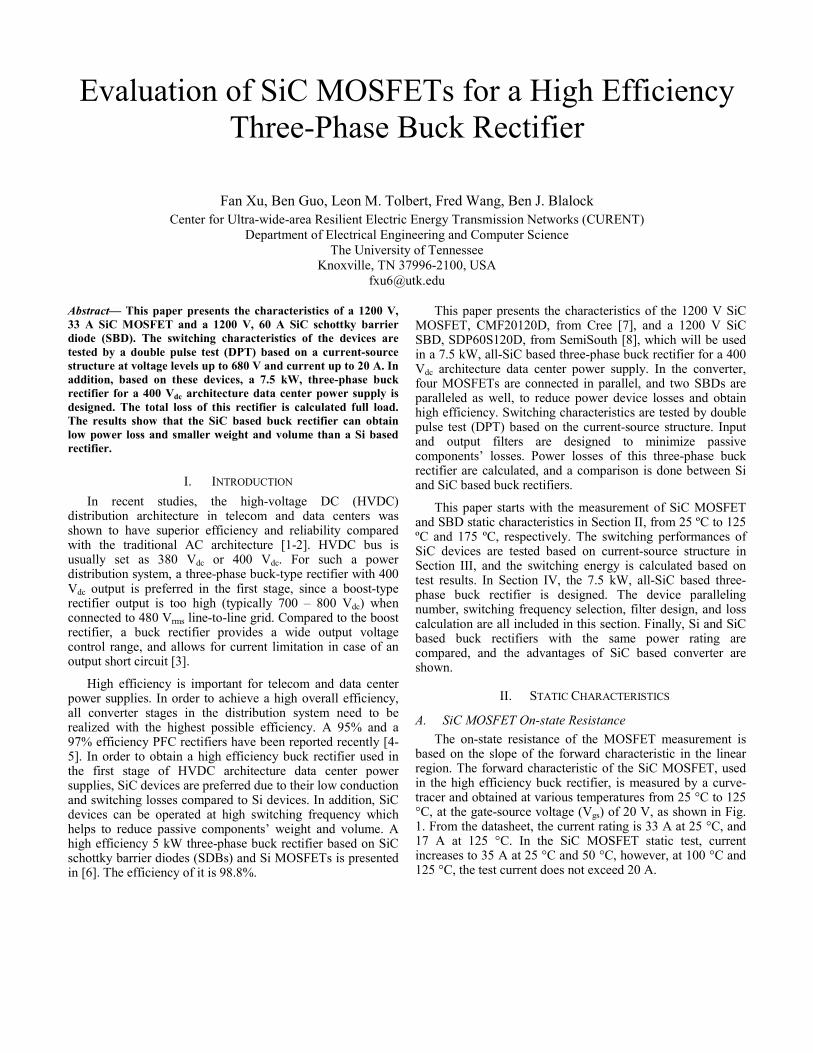
A. SiC MOSFET On-state Resistance The on-state resistance of the MOSFET measurement is
based on the slope of the forward characteristic in the linear region. The forward characteristic of the SiC MOSFET, used in the high efficiency buck rectifier, is measured by a curve-tracer and obtained at various temperatures from 25 °C to 125 °C, at the gate-source voltage (Vgs) of 20 V, as shown in Fig. 1. From the datasheet, the current rating is 33 A at 25 °C, and 17 A at 125 °C. In the SiC MOSFET static test, current increases to 35 A at 25 °C and 50 °C, however, at 100 °C and 125 °C, the test current does not exceed 20 A.
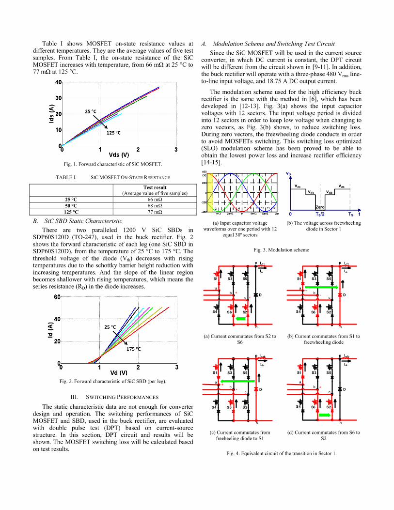
Table I shows MOSFET on-state resistance values at different temperatures. They are the average values of five test samples. From Table I, the on-state resistance of the SiC MOSFET increases with temperature, from 66 mΩ at 25 °C to 77 mΩ at 125 °C.
Fig. 1. Forward characteristic of SiC MOSFET.
TABLE I. SIC MOSFET ON-STATE RESISTANCE
Test result (Average value of five samples)
25 °C 66 mΩ 50 °C 68 mΩ 125 °C 77 mΩ
B. SiC SBD Static Characteristic There are two paralleled 1200 V SiC SBDs in
SDP60S120D (TO-247), used in the buck rectifier. Fig. 2 shows the forward characteristic of each leg (one SiC SBD in SDP60S120D), from the temperature of 25 °C to 175 °C. The threshold voltage of the diode (Vth) decreases with rising temperatures due to the schottky barrier height reduction with increasing temperatures. And the slope of the linear region becomes shallower with rising temperatures, which means the series resistance (RD) in the diode increases.
Fig. 2. Forward characteristic of SiC SBD (per leg).
III. SWITCHING PERFORMANCES The static characteristic data are not enough for converter
design and operation. The switching performances of SiC MOSFET and SBD, used in the buck rectifier, are evaluated with double pulse test (DPT) based on current-source structure. In this section, DPT circuit and results will be shown. The MOSFET switching loss will be calculated based on test results.
A. Modulation Scheme and Switching Test Circuit Since the SiC MOSFET will be used in the current source
converter, in which DC current is constant, the DPT circuit will be different from the circuit shown in [9-11]. In addition, the buck rectifier will operate with a three-phase 480 Vrms line-to-line input voltage, and 18.75 A DC output current.
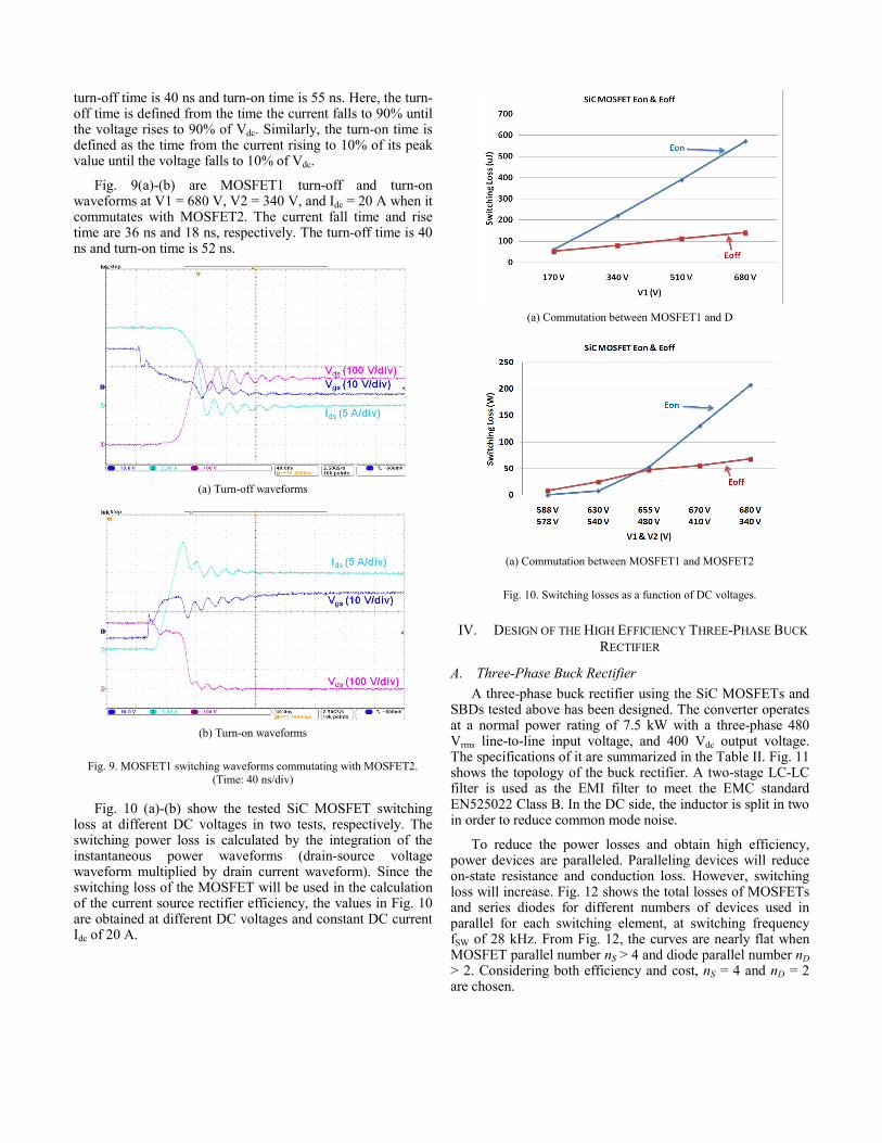
The modulation scheme used for the high efficiency buck rectifier is the same with the method in [6], which has been developed in [12-13]. Fig. 3(a) shows the input capacitor voltages with 12 sectors. The input voltage period is divided into 12 sectors in order to keep low voltage when changing to zero vectors, as Fig. 3(b) shows, to reduce switching loss. During zero vectors, the freewheeling diode conducts in order to avoid MOSFETs switching. This switching loss optimized (SLO) modulation scheme has been proved to be able to obtain the lowest power loss and increase rectifier efficiency [14-15].
(a) Input capacitor voltage
waveforms over one period with 12 equal 30º sectors
(b) The voltage across freewheeling diode in Sector 1
Fig. 3. Modulation scheme
Ld c
S1
S4
S5S3
S6 S2
Idc
D
ab
c
p
n
+-
Ldc
S1
S4
S5S3
S6 S2
Idc
D
ab
c
p
n
+-
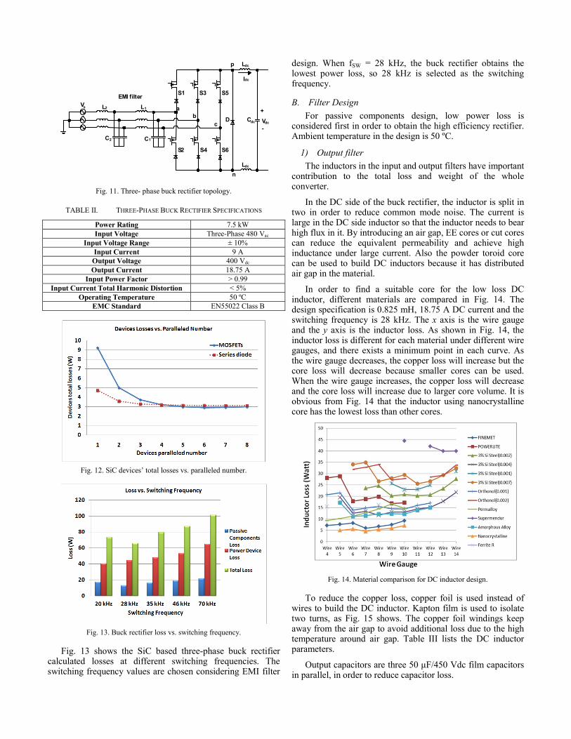
(a) Current commutates from S2 to S6
(b) Current commutates from S1 to freewheeling diode
Ldc
S1
S4
S5S3
S6 S2
Idc
D
ab
c
p
n
+-
Ldc
S1
S4
S5S3
S6 S2
Idc
D
ab
c
p
n
+-
(c) Current commutates from freeheeling diode to S1
(d) Current commutates from S6 to S2
Fig. 4. Equivalent circuit of the transition in Sector 1.

Fig. 4(a)-(d) show the transition process in Sector 1 (0 ~ 30º) (as Fig. 3(a)-(b) show), based on the chosen modulation method. In Sector 1, commutation happens between S1 and freewheeling diode (D), or between S2 and S6. According to the input voltage value, Vab decreases from 680 V to 340 V when current commutates between S1 and D. Meanwhile, Vab decreases from 588 V to 340 V, and Vac increases from 588 V to 680 V when current commutates between S2 and S6.
Fig. 5 shows the current source DPT circuit. In the first test, MOSFET2 is turned off and the double pulse signal is added to the gate of MOSFET1, current commutates between MOSFET1 and D. V1 increases from 340 V to 680 V. In the second test, a pulse is added to the gate of MOSFET2 too. The overlap time is 1 μs. V1 increases from 588 V to 680 V, and V2 decreases from 588 V to 340 V. Current commutates between MOSEFT1 and MOSFET2. The load is a 1 mH inductor.
Load Ldc
MOSFET1
Idc
D
V1
i1
Vds+
-
MOSFET2
V2
i2
D1 D2
Fig. 5. Current source double pulse test circuit.
Fig. 6. Double pulse test waveforms. (Time: 4 μs/div)
Fig. 6 shows DPT waveforms. The load inductor is charged to rated current value during the first pulse. When MOSFET1 is turned off, load current commutates to freewheeling diode or MOSFET2. The load current commutates back to MOSFET1 when it is turned on during the second pulse.
The driver IC of SiC MOSFET is IXDN514, which is based on PMOS-NMOS totem-pole structure. The gate voltage of +20 V is chosen for MOSFET turning on and -3 V is used for its turning off. The external gate resistance is 5 Ω. Probe Tip Adapter (PTA) is used to measure the gate-source voltage Vgs. The drain-source voltage Vds is measured by
differential probe. The current probe is used to measure MOSFET drain current Ids. Fig. 7 shows the test setup.
Fig. 7. Double pulse test setup.
B. Test Waveforms and Switching Loss
(a) Turn-off waveforms
(b) Turn-on waveforms
Fig. 8. MOSFET1 switching waveforms commutating with freewheeling diode (D). (Time: 40 ns/div)
Fig. 8(a)-(b) are MOSFET1 turn-off and turn-on waveforms, respectively, when it commutates with freewheeling diode D. V1 = 680 V, Idc = 20 A, and MOSFET2 is turned off. The current fall time and rise time during turn-off and turn-on transient are 40 ns and 14 ns, respectively. The
turn-off time is 40 ns and turn-on time is 55 ns. Here, the turn-off time is defined from the time the current falls to 90% until the voltage rises to 90% of Vdc. Similarly, the turn-on time is defined as the time from the current rising to 10% of its peak value until the voltage falls to 10% of Vdc.
Fig. 9(a)-(b) are MOSFET1 turn-off and turn-on waveforms at V1 = 680 V, V2 = 340 V, and Idc = 20 A when it commutates with MOSFET2. The current fall time and rise time are 36 ns and 18 ns, respectively. The turn-off time is 40 ns and turn-on time is 52 ns.
(a) Turn-off waveforms
(b) Turn-on waveforms
Fig. 9. MOSFET1 switching waveforms commutating with MOSFET2. (Time: 40 ns/div)
Fig. 10 (a)-(b) show the tested SiC MOSFET switching loss at different DC voltages in two tests, respectively. The switching power loss is calculated by the integration of the instantaneous power waveforms (drain-source voltage waveform multiplied by drain current waveform). Since the switching loss of the MOSFET will be used in the calculation of the current source rectifier efficiency, the values in Fig. 10 are obtained at different DC voltages and constant DC current Idc of 20 A.
(a) Commutation between MOSFET1 and D
(a) Commutation between MOSFET1 and MOSFET2
Fig. 10. Switching losses as a function of DC voltages.
IV. DESIGN OF THE HIGH EFFICIENCY THREE-PHASE BUCK RECTIFIER
A. Three-Phase Buck Rectifier A three-phase buck rectifier using the SiC MOSFETs and
SBDs tested above has been designed. The converter operates at a normal power rating of 7.5 kW with a three-phase 480 Vrms line-to-line input voltage, and 400 Vdc output voltage. The specifications of it are summarized in the Table II. Fig. 11 shows the topology of the buck rectifier. A two-stage LC-LC filter is used as the EMI filter to meet the EMC standard EN525022 Class B. In the DC side, the inductor is split in two in order to reduce common mode noise.
To reduce the power losses and obtain high efficiency, power devices are paralleled. Paralleling devices will reduce on-state resistance and conduction loss. However, switching loss will increase. Fig. 12 shows the total losses of MOSFETs and series diodes for different numbers of devices used in parallel for each switching element, at switching frequency fSW of 28 kHz. From Fig. 12, the curves are nearly flat when MOSFET parallel number nS > 4 and diode parallel number nD > 2. Considering both efficiency and cost, nS = 4 and nD = 2 are chosen.
EMI filter
Cdc
L1
Ldc
C1
S1
S2
S5S3
S4 S6
Idc
+
-VdcD
ab
c
p
n
Vs L2
C2
Ldc
Fig. 11. Three- phase buck rectifier topology.
TABLE II. THREE-PHASE BUCK RECTIFIER SPECIFICATIONS
Power Rating 7.5 kW Input Voltage Three-Phase 480 Vac
Input Voltage Range ± 10% Input Current 9 A
Output Voltage 400 Vdc Output Current 18.75 A
Input Power Factor > 0.99 Input Current Total Harmonic Distortion < 5%
Operating Temperature 50 ºC EMC Standard EN55022 Class B
Fig. 12. SiC devices’ total losses vs. paralleled number.
Fig. 13. Buck rectifier loss vs. switching frequency.
Fig. 13 shows the SiC based three-phase buck rectifier calculated losses at different switching frequencies. The switching frequency values are chosen considering EMI filter
design. When fSW = 28 kHz, the buck rectifier obtains the lowest power loss, so 28 kHz is selected as the switching frequency.
B. Filter Design For passive components design, low power loss is
considered first in order to obtain the high efficiency rectifier. Ambient temperature in the design is 50 ºC.
1) Output filter The inductors in the input and output filters have important
contribution to the total loss and weight of the whole converter.
In the DC side of the buck rectifier, the inductor is split in two in order to reduce common mode noise. The current is large in the DC side inductor so that the inductor needs to bear high flux in it. By introducing an air gap, EE cores or cut cores can reduce the equivalent permeability and achieve high inductance under large current. Also the powder toroid core can be used to build DC inductors because it has distributed air gap in the material.
In order to find a suitable core for the low loss DC inductor, different materials are compared in Fig. 14. The design specification is 0.825 mH, 18.75 A DC current and the switching frequency is 28 kHz. The x axis is the wire gauge and the y axis is the inductor loss. As shown in Fig. 14, the inductor loss is different for each material under different wire gauges, and there exists a minimum point in each curve. As the wire gauge decreases, the copper loss will increase but the core loss will decrease because smaller cores can be used. When the wire gauge increases, the copper loss will decrease and the core loss will increase due to larger core volume. It is obvious from Fig. 14 that the inductor using nanocrystalline core has the lowest loss than other cores.
Fig. 14. Material comparison for DC inductor design.
To reduce the copper loss, copper foil is used instead of wires to build the DC inductor. Kapton film is used to isolate two turns, as Fig. 15 shows. The copper foil windings keep away from the air gap to avoid additional loss due to the high temperature around air gap. Table III lists the DC inductor parameters.
Output capacitors are three 50 μF/450 Vdc film capacitors in parallel, in order to reduce capacitor loss.
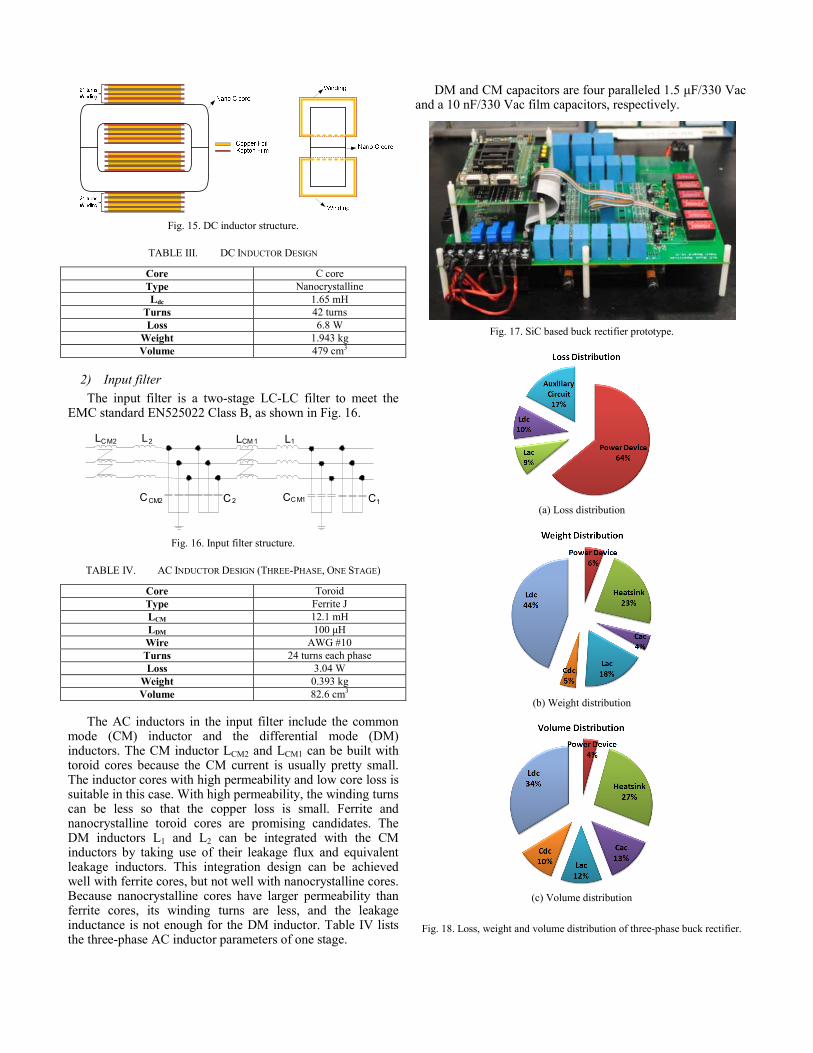
Fig. 15. DC inductor structure.
TABLE III. DC INDUCTOR DESIGN
Core C core Type Nanocrystalline Ldc 1.65 mH
Turns 42 turns Loss 6.8 W
Weight 1.943 kg Volume 479 cm3
2) Input filter The input filter is a two-stage LC-LC filter to meet the
EMC standard EN525022 Class B, as shown in Fig. 16.
L1L2
CCM2
LCM2 LCM 1
C2 C1CCM1
Fig. 16. Input filter structure.
TABLE IV. AC INDUCTOR DESIGN (THREE-PHASE, ONE STAGE)
Core Toroid Type Ferrite J LCM 12.1 mH LDM 100 μH Wire AWG #10 Turns 24 turns each phase Loss 3.04 W
Weight 0.393 kg Volume 82.6 cm3
The AC inductors in the input filter include the common mode (CM) inductor and the differential mode (DM) inductors. The CM inductor LCM2 and LCM1 can be built with toroid cores because the CM current is usually pretty small. The inductor cores with high permeability and low core loss is suitable in this case. With high permeability, the winding turns can be less so that the copper loss is small. Ferrite and nanocrystalline toroid cores are promising candidates. The DM inductors L1 and L2 can be integrated with the CM inductors by taking use of their leakage flux and equivalent leakage inductors. This integration design can be achieved well with ferrite cores, but not well with nanocrystalline cores. Because nanocrystalline cores have larger permeability than ferrite cores, its winding turns are less, and the leakage inductance is not enough for the DM inductor. Table IV lists the three-phase AC inductor parameters of one stage.
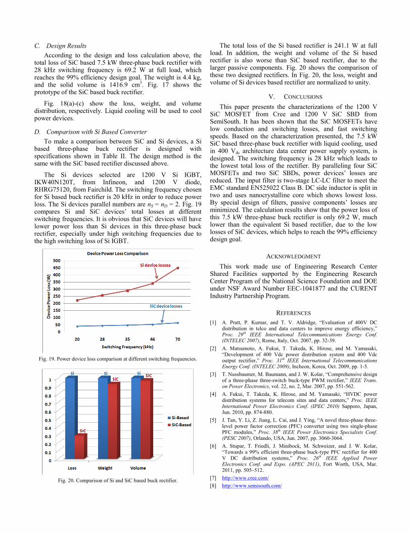
DM and CM capacitors are four paralleled 1.5 μF/330 Vac and a 10 nF/330 Vac film capacitors, respectively.
Fig. 17. SiC based buck rectifier prototype.
(a) Loss distribution
(b) Weight distribution
(c) Volume distribution
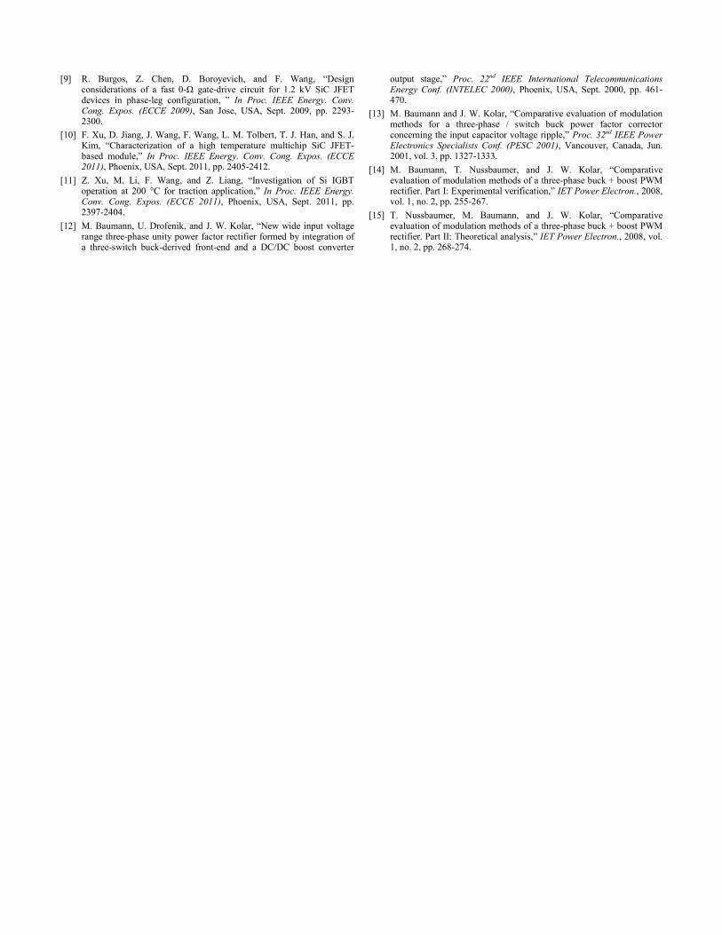
Fig. 18. Loss, weight and volume distribution of three-phase buck rectifier.
C. Design Results According to the design and loss calculation above, the
total loss of SiC based 7.5 kW three-phase buck rectifier with 28 kHz switching frequency is 69.2 W at full load, which reaches the 99% efficiency design goal. The weight is 4.4 kg, and the solid volume is 1416.9 cm3. Fig. 17 shows the prototype of the SiC based buck rectifier.
Fig. 18(a)-(c) show the loss, weight, and volume distribution, respectively. Liquid cooling will be used to cool power devices.
D. Comparison with Si Based Converter To make a comparison between SiC and Si devices, a Si
based three-phase buck rectifier is designed with specifications shown in Table II. The design method is the same with the SiC based rectifier discussed above.
The Si devices selected are 1200 V Si IGBT, IKW40N120T, from Infineon, and 1200 V diode, RHRG75120, from Fairchild. The switching frequency chosen for Si based buck rectifier is 20 kHz in order to reduce power loss. The Si devices parallel numbers are nS = nD = 2. Fig. 19 compares Si and SiC devices’ total losses at different switching frequencies. It is obvious that SiC devices will have lower power loss than Si devices in this three-phase buck rectifier, especially under high switching frequencies due to the high switching loss of Si IGBT.
Fig. 19. Power device loss comparison at different switching frequencies.
Fig. 20. Comparison of Si and SiC based buck rectifier.
The total loss of the Si based rectifier is 241.1 W at full load. In addition, the weight and volume of the Si based rectifier is also worse than SiC based rectifier, due to the larger passive components. Fig. 20 shows the comparison of these two designed rectifiers. In Fig. 20, the loss, weight and volume of Si devices based rectifier are normalized to unity.
V. CONCLUSIONS This paper presents the characterizations of the 1200 V
SiC MOSFET from Cree and 1200 V SiC SBD from SemiSouth. It has been shown that the SiC MOSFETs have low conduction and switching losses, and fast switching speeds. Based on the characterization presented, the 7.5 kW SiC based three-phase buck rectifier with liquid cooling, used in 400 Vdc architecture data center power supply system, is designed. The switching frequency is 28 kHz which leads to the lowest total loss of the rectifier. By paralleling four SiC MOSFETs and two SiC SBDs, power devices’ losses are reduced. The input filter is two-stage LC-LC filter to meet the EMC standard EN525022 Class B. DC side inductor is split in two and uses nanocrystalline core which shows lowest loss. By special design of filters, passive components’ losses are minimized. The calculation results show that the power loss of this 7.5 kW three-phase buck rectifier is only 69.2 W, much lower than the equivalent Si based rectifier, due to the low losses of SiC devices, which helps to reach the 99% efficiency design goal.
ACKNOWLEDGMENT This work made use of Engineering Research Center
Shared Facilities supported by the Engineering Research Center Program of the National Science Foundation and DOE under NSF Award Number EEC-1041877 and the CURENT Industry Partnership Program.
REFERENCES [1] A. Pratt, P. Kumar, and T. V. Aldridge, “Evaluation of 400V DC
distribution in telco and data centers to improve energy efficiency,” Proc. 29th IEEE International Telecommunications Energy Conf. (INTELEC 2007), Rome, Italy, Oct. 2007, pp. 32-39.
[2] A. Matsumoto, A. Fukui, T. Takeda, K. Hirose, and M. Yamasaki, “Development of 400 Vdc power distribution system and 400 Vdc output rectifier,” Proc. 31th IEEE International Telecommunications Energy Conf. (INTELEC 2009), Incheon, Korea, Oct. 2009, pp. 1-5.
[3] T. Nussbaumer, M. Baumann, and J. W. Kolar, “Comprehensive design of a three-phase three-switch buck-type PWM rectifier,” IEEE Trans. on Power Electronics, vol. 22, no. 2, Mar. 2007, pp. 551-562.
[4] A. Fukui, T. Takeda, K. Hirose, and M. Yamasaki, “HVDC power distribution systems for telecom sites and data centers,” Proc. IEEE International Power Electronics Conf. (IPEC 2010) Sapporo, Japan, Jun. 2010, pp. 874-880.
[5] J. Tan, Y. Li, Z. Jiang, L. Cai, and J. Ying, “A novel three-phase three-level power factor correction (PFC) converter using two single-phase PFC modules,” Proc. 38th IEEE Power Electronics Specialists Conf. (PESC 2007), Orlando, USA, Jun. 2007, pp. 3060-3064.
[6] A. Stupar, T. Friedli, J. Minibock, M. Schweizer, and J. W. Kolar, “Towards a 99% efficient three-phase buck-type PFC rectifier for 400 V DC distribution systems,” Proc. 26th IEEE Applied Power Electronics Conf. and Expo. (APEC 2011), Fort Worth, USA, Mar. 2011, pp. 505–512.
[7] http://www.cree.com/ [8] http://www.semisouth.com/
[9] R. Burgos, Z. Chen, D. Boroyevich, and F. Wang, “Design considerations of a fast 0-Ω gate-drive circuit for 1.2 kV SiC JFET devices in phase-leg configuration, ” In Proc. IEEE Energy. Conv. Cong. Expos. (ECCE 2009), San Jose, USA, Sept. 2009, pp. 2293-2300.
[10] F. Xu, D. Jiang, J. Wang, F. Wang, L. M. Tolbert, T. J. Han, and S. J. Kim, “Characterization of a high temperature multichip SiC JFET-based module,” In Proc. IEEE Energy. Conv. Cong. Expos. (ECCE 2011), Phoenix, USA, Sept. 2011, pp. 2405-2412.
[11] Z. Xu, M. Li, F. Wang, and Z. Liang, “Investigation of Si IGBT operation at 200 °C for traction application,” In Proc. IEEE Energy. Conv. Cong. Expos. (ECCE 2011), Phoenix, USA, Sept. 2011, pp. 2397-2404.
[12] M. Baumann, U. Drofenik, and J. W. Kolar, “New wide input voltage range three-phase unity power factor rectifier formed by integration of a three-switch buck-derived front-end and a DC/DC boost converter
output stage,” Proc. 22nd IEEE International Telecommunications Energy Conf. (INTELEC 2000), Phoenix, USA, Sept. 2000, pp. 461-470.
[13] M. Baumann and J. W. Kolar, “Comparative evaluation of modulation methods for a three-phase / switch buck power factor corrector concerning the input capacitor voltage ripple,” Proc. 32nd IEEE Power Electronics Specialists Conf. (PESC 2001), Vancouver, Canada, Jun. 2001, vol. 3, pp. 1327-1333.
[14] M. Baumann, T. Nussbaumer, and J. W. Kolar, “Comparative evaluation of modulation methods of a three-phase buck + boost PWM rectifier. Part I: Experimental verification,” IET Power Electron., 2008, vol. 1, no. 2, pp. 255-267.
[15] T. Nussbaumer, M. Baumann, and J. W. Kolar, “Comparative evaluation of modulation methods of a three-phase buck + boost PWM rectifier. Part II: Theoretical analysis,” IET Power Electron., 2008, vol. 1, no. 2, pp. 268-274.