e_s-1w & f_s-1w_en
TRANSCRIPT
8/13/2019 E_S-1W & F_S-1W_EN
http://slidepdf.com/reader/full/es-1w-fs-1wen 1/5
8/13/2019 E_S-1W & F_S-1W_EN
http://slidepdf.com/reader/full/es-1w-fs-1wen 2/5
The copyright and authority for the interpretation of the products are reserved by MORNSUN E_S-1W&F_S-1W B/1-2012 Page 2 of 5
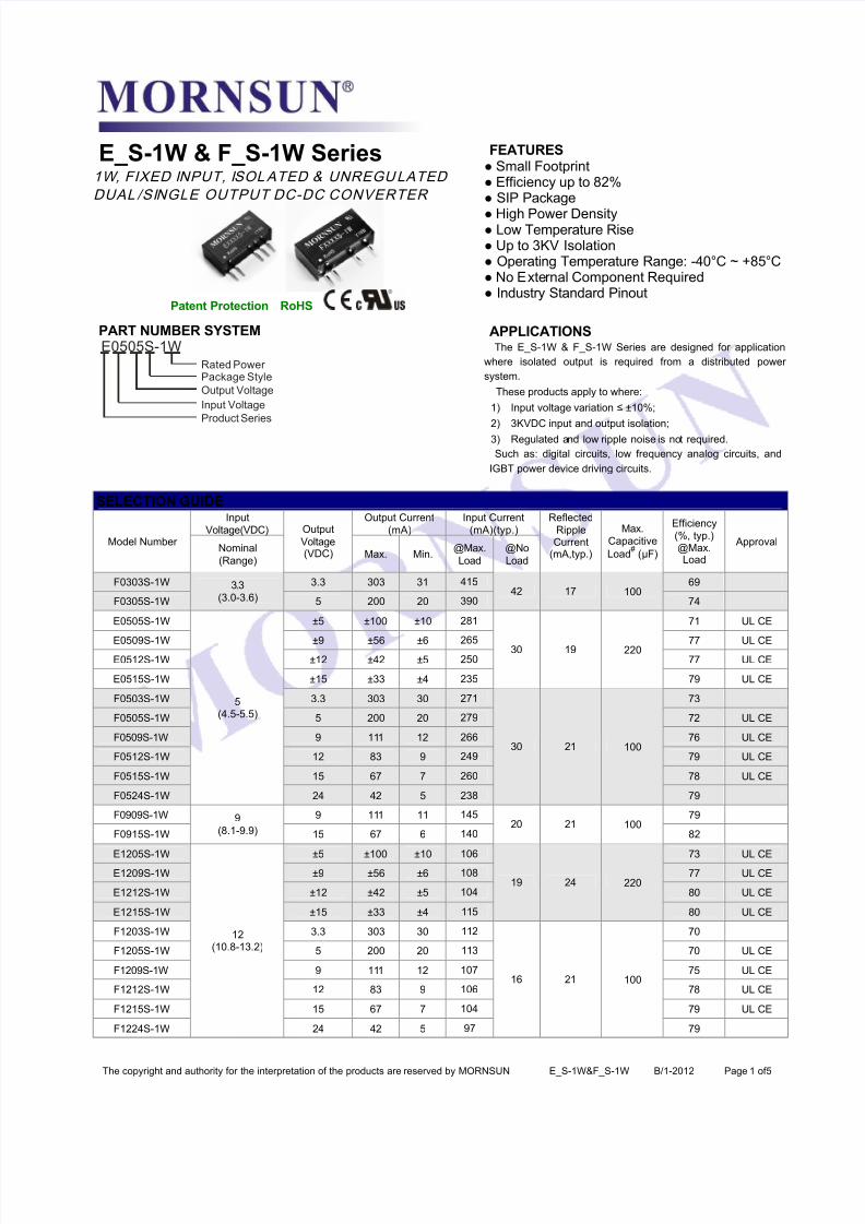
Input
Voltage(VDC)
Output Current
(mA)
Input Current
(mA)(typ.)Model Number
Nominal(Range)
Output
Voltage(VDC) Max. Min.
@Max.Load
@NoLoad
Reflected
RippleCurrent
(mA,typ.)
Max.
Capacitive
Load# ($F)
Efficiency
(%, typ.)@Max.Load
Approval
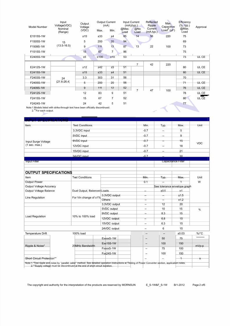
E1515S-1W #15 #33 #4 85 14 56 220 75
F1505S-1W 5 200 20 94 69
F1509S-1W 9 111 12 87 73
F1515S-1W
15(13.5-16.5)
15 67 7 86
13 22 100
75
E2405S-1W #5 #100 #10 53 73 UL CE
E2409S-1W #9 #56 #6 52 77 UL CE
E2412S-1W #12 #42 #5 51 80 UL CE
E2415S-1W #15 #33 #4 51
7 42 220
80 UL CE
F2403S-1W 3.3 303 31 56 70
F2405S-1W 5 200 20 56 71 UL CE
F2409S-1W 9 111 12 52 76 UL CE
F2412S-1W 12 83 9 51 78 UL CE
F2415S-1W 15 67 7 52 80 UL CE
F2424S-1W
24(21.6-26.4)
24 42 5 51
7 47 100
77
Note:1.Models listed with strike-through text have been officially discontinued.
2. #
For each output.
INPUT SPECIFICATIONS
Item Test Conditions Min. Typ. Max. Unit
3.3VDC input -0.7 -- 5
5VDC input -0.7 -- 9
9VDC input -0.7 -- 15
12VDC input -0.7 -- 18
15VDC input -0.7 -- 21
Input Surge Voltage(1 sec. max.)
24VDC input -0.7 -- 30
VDC
Input Filter Capacitance Filter
OUTPUT SPECIFICATIONS
Item Test Conditions Min. Typ. Max. Unit
Output Power 0.1 -- 1 W
Output Voltage Accuracy See tolerance envelope graph
Output Voltage Balance Dual Output, Balanced Loads -- #0.5 #1
3.3VDC output -- -- #1.5Line Regulation For Vin change of #1%
Others -- -- #1.2
3.3VDC output -- 12 20
5VDC output -- 10 15
9VDC output -- 8.3 15
12VDC output -- 6.8 15
15VDC output -- 6.3 15
Load Regulation 10% to 100% load
24VDC output -- 6 15
%
Temperature Drift 100% load -- -- #0.03 %/!C
ExxxxS-1W -- 50 75
Exx15S-1W -- 100 150
FxxxxS-1W -- 75 100Ripple & Noise* 20MHz Bandwidth
Fxx24S-1W -- 100 150
mVp-p
Short Circuit Protection** -- -- 1 s
Note:1.*Test ripple and noise by %parallel cable& method. See detailed operation instructions at Testing of Power Converter section, application notes.
2.**Supply voltage must be discontinued at the end of short circuit duration.
8/13/2019 E_S-1W & F_S-1W_EN
http://slidepdf.com/reader/full/es-1w-fs-1wen 3/5
The copyright and authority for the interpretation of the products are reserved by MORNSUN E_S-1W&F_S-1W B/1-2012 Page 3 of 5
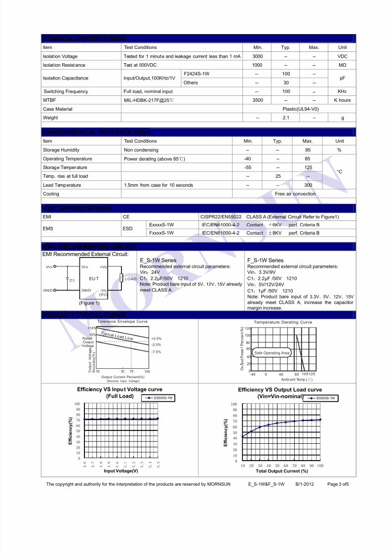
COMMON SPECIFICATIONS
Item Test Conditions Min. Typ. Max. Unit
Isolat ion Voltage Tested for 1 minute and leakage current less than 1 mA 3000 -- -- VDC
Isolat ion Resistance Test at 500VDC 1000 -- -- M'
F2424S-1W -- 100 --Isolation Capacitance Input/Output,100KHz/1V
Others -- 30 --pF
Switching Frequency Full load, nominal input -- 100 -- KHz
MTBF MIL-HDBK-217F@25 3500 -- -- K hours
Case Material Plastic(UL94-V0)
Weight -- 2.1 -- g
ENVIRONMENTAL SPECIFICATIONS
Item Test Conditions Min. Typ. Max. Unit
Storage Humidity Non condensing -- -- 95 %
Operating Temperature Power derating (above 85) -40 -- 85
Storage Temperature -55 -- 125
Temp. rise at full load -- 25 --
Lead Temperature 1.5mm from case for 10 seconds -- -- 300
!C
Cooling Free air convection
EMC SPECIFICATIONS
EMI CE CISPR22/EN55022 CLASS A (External Circuit Refer to Figure1)
ExxxxS-1W IEC/EN61000-4-2 Contact !6KV perf. Criteria BEMS ESD
FxxxxS-1W IEC/EN61000-4-2 Contact !8KV perf. Criteria B
EMC RECOMMENDED CIRCUITEMI Recommended External Circuit:
Vin
GN D
+Vo
-Vo(0V)
EU T LOADC1
Vin
GND
(Figure 1)
E_S-1W SeriesRecommended external circuit parameters: Vin"24V
C1"2.2$F/50V 1210
Note: Product bare input of 5V12V15V already
meet CLASS A.
F_S-1W SeriesRecommended external circuit parameters:
Vin"3.3V/9V
C1"2.2$F /50V 1210
Vin"5V/12V/24V
C1"1$F /50V 1210Note: Product bare input of 3.3V5V12V15V
already meet CLASS A, increase the capacitormargin increase.
PRODUCT TYPICAL CURVETolerance Envelope Curve
+10%
+5%
50 100
+2.5%
-2.5%
-7.5%
Rated OutputVoltage
OutputVoltage
(%)
Accuracy
Output Current Percent(%)
T y p i c a l Lo a d Li n e
70
(Nominal Input Voltage)
120
100
80
60
40
20
0-40 0 40 85 105120
O u p u t P o w e
P e r c e n t % )
Ambi ent Temp.( )
Temperature Derating Curve
Safe Operating Area
Efficiency VS Input Voltage curve(Full Load)
0
10
20
30
40
50
60
70
80
90
100
4 .
6
4 .
7
4 .
8
4 .
9
5 .
0
5 .
1
5 .
2
5 .
3
5 .
4
5 .
5
Input Voltage(V)
E f f i c i e n c y ( % )
E0505S-1W
Efficiency VS Output Load curve(Vin=Vin-nominal)
0
10
20
30
40
50
60
70
80
90
100
10 20 30 40 50 60 70 80 90 1 00
Total Output Current (%)
E f f i c i e n c y ( % )
E0505S-1W
8/13/2019 E_S-1W & F_S-1W_EN
http://slidepdf.com/reader/full/es-1w-fs-1wen 4/5
The copyright and authority for the interpretation of the products are reserved by MORNSUN E_S-1W&F_S-1W B/1-2012 Page 4 of 5
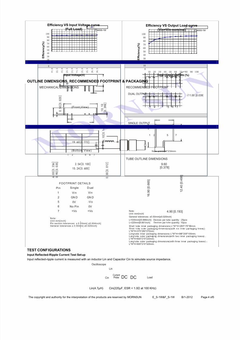
Efficiency VS Input Voltage curve
(Full Load)
0
10
20
30
40
50
60
70
80
90
100
2 2 .
0
2 2 .
5
2 3 .
0
2 3 .
5
2 4 .
0
2 4 .
5
2 5 .
0
2 5 .
5
2 6 .
0
2 6 .
5
Input Voltage(V)
E f f i c i e n c y ( % )
F2405S-1W
Efficiency VS Output Load curve
(Vin=Vin-nominal)
0
10
20
30
40
50
60
70
80
90
100
10 20 30 40 50 60 70 80 90 100
Total Output Current (%)
E
f f i c i e n c y ( % )
F2405S-1W
OUTLINE DIMENSIONS, RECOMMENDED FOOTPRINT & PACKAGING
DUAL OUTPUT
SINGLE OUTPUT
1
6
2
7
Vi n
GN D
0V
+Vo
5
No Pin
Vin
GN D
0V
+Vo
-Vo
Pin Single Dual
FOOTPRINT DETAILS
Note:Unit:mm[inch]Pin section tolerances: # 0.10mm[ #0.004inch]General tolerances:# 0.50mm[ #0.020inch]
MECHANICAL DIMENSIONS RECOMMENDED FOOTPRINT
TUBE OUTLINE DIMENSIONS
Note:
Unit :mm[inch]
General tolerances: #0.50mm[#0.020inch]
L=530mm[20.866inch] Devices per tube quantity : 25pcs
L=220mm[8.661inch] Devices per tube quantity: 10pcs
(Bottom View)
(Front View)
Short tube inner packaging dimensions: L*W*H=255*170*80mm;Short tube outer packaging dimensions(with six inner packaging boxes):
"
"
L*W*H=375*280*270mm;
Long tube inner packaging dimensions: L*W*H=580*200*100mm;Long tube outer packaging dimensions(with two inner packaging boxes)
L*W*H=600*215*220mm;Long tube outer packaging dimensions(with three inner packaging boxes)L*W*H=600*215*325mm.
Note grid 2.54*2.54mm: .
51 2 7
1.00 [0.039]
1 2 5 6 7
9.60 [0.378]
1 2 . 4
0 [ 0 . 4 8
8 ]
1 6 . 9
0 [ 0 . 6
6 5 ]
4.90 [0.193]
1 2 5 76
19.60[0.772]
1 0 .
1 0
[ 0 .
3 9 8 ]
4 .
1 0
[ 0 .
1 6 1 ]
0 .
5 0
[ 0 .
0 2 0 ]
0.50[0.020]
0 .
9 0
[ 0 .
0 3 5 ]
0 .
3 0
[ 0 .
0 1 2 ]
15.24[0.600]
2.54[0.100]
6 .
0 0
[ 0 .
2 3 6 ]
TEST CONFIGURATIONS
Input Reflected-Ripple Current Test Setup
Input reflected-ripple current is measured with an inductor Lin and Capacitor Cin to simulate source impedance.
DCCin
Lin
DC Load
Oscilloscope
Current Probe
Lin(4.7$H) Cin(220$F, ESR < 1.0' at 100 KHz)
8/13/2019 E_S-1W & F_S-1W_EN
http://slidepdf.com/reader/full/es-1w-fs-1wen 5/5
The copyright and authority for the interpretation of the products are reserved by MORNSUN E_S-1W&F_S-1W B/1-2012 Page 5 of 5
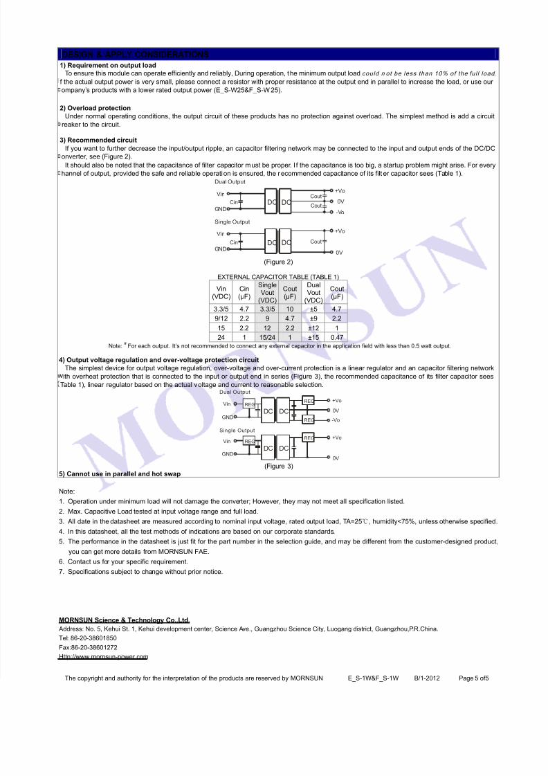
DESIGN & APPLY CONSIDERATIONS
1) Requirement on output load
To ensure this module can operate efficiently and reliably, During operation, the minimum output load could n ot be less than 10% of the ful l load .
f the actual output power is very small, please connect a resistor with proper resistance at the output end in parallel to increase the load, or use our
ompany(s products with a lower rated output power (E_S-W25&F_S-W 25).
2) Overload protection
Under normal operating conditions, the output circuit of these products has no protection against overload. The simplest method is add a circuit
reaker to the circuit.
3) Recommended circuit
If you want to further decrease the input/output ripple, an capacitor filtering network may be connected to the input and output ends of the DC/DC
onverter, see (Figure 2). It should also be noted that the capacitance of filter capacitor must be proper. I f the capacitance is too big, a startup problem might arise. For every
hannel of output, provided the safe and reliable operation is ensured, the recommended capacitance of its filt er capacitor sees (Table 1).
Vin
GND
+Vo
0VDCCin DCCout
Cout
-Vo
Dual Output
Single Output
Vin
GND
+Vo
0V
DCCin DC Cout
(Figure 2)
EXTERNAL CAPACITOR TABLE (TABLE 1)
Vin
(VDC)Cin($F)
SingleVout
(VDC)
Cout($F)
DualVout
(VDC)
Cout($F)
3.3/5 4.7 3.3/5 10 #5 4.7
9/12 2.2 9 4.7 #9 2.2
15 2.2 12 2.2 #12 1
24 1 15/24 1 #15 0.47
Note: # For each output. It(s not recommended to connect any external capacitor in the application field with less than 0.5 watt output.
4) Output voltage regulation and over-voltage protection circuit
The simplest device for output voltage regulation, over-voltage and over-current protection is a linear regulator and an capacitor filtering network
ith overheat protection that is connected to the input or output end in series (Figure 3), the recommended capacitance of its filter capacitor sees
Table 1), linear regulator based on the actual voltage and current to reasonable selection.
Vin
GND
0V
+Vo
DC DC
-Vo
REGREG
REG
Vin
GND0V
+Vo
DC DCREG
REG
Dual Output
Single Output
(Figure 3)
5) Cannot use in parallel and hot swap
Note:
1. Operation under minimum load will not damage the converter; However, they may not meet all specification listed.
2. Max. Capacitive Load tested at input voltage range and full load.
3. All date in the datasheet are measured according to nominal input voltage, rated output load, TA=25 , humidity<75%, unless otherwise specified .
4. In this datasheet, all the test methods of indications are based on our corporate standards.
5. The performance in the datasheet is just fit for the part number in the selection guide, and may be different from the customer-designed product,you can get more details from MORNSUN FAE.
6. Contact us for your specific requirement.
7. Specifications subject to change without prior notice.
MORNSUN Science & Technology Co.,Ltd.
Address: No. 5, Kehui St. 1, Kehui development center, Science Ave., Guangzhou Science City, Luogang district, Guangzhou,P.R.China.
Tel: 86-20-38601850
Fax:86-20-38601272
Http://www.mornsun-power.com