engn 2211 electronic circuits and devices problem set...
TRANSCRIPT
ANU ENGN 2211
AUSTRALIAN NATIONAL UNIVERSITYDepartment of Engineering
ENGN 2211 Electronic Circuits and DevicesProblem Set #8 BJT CE Amplifier Circuits
Q1
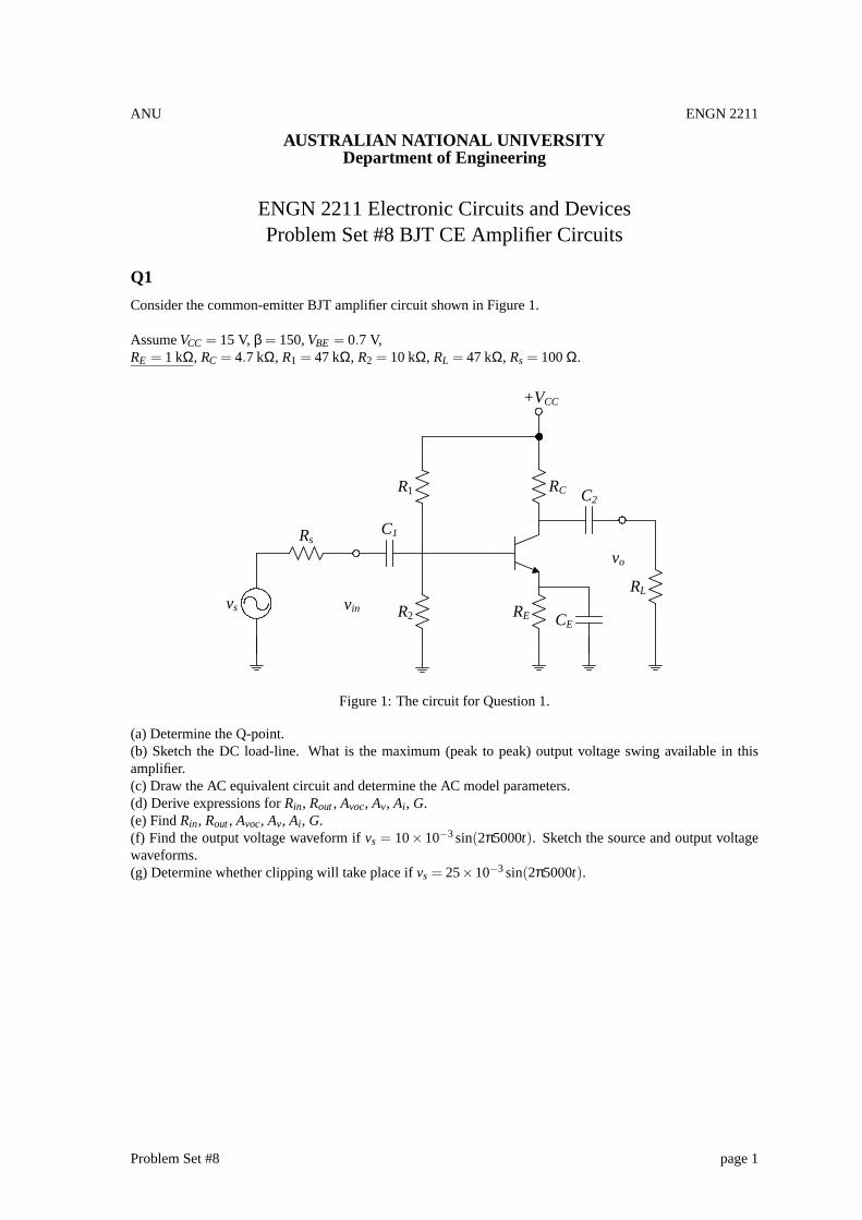
Consider the common-emitter BJT amplifier circuit shown in Figure 1.
AssumeVCC = 15 V, β = 150,VBE = 0.7 V,RE = 1 kΩ, RC = 4.7 kΩ, R1 = 47 kΩ, R2 = 10 kΩ, RL = 47 kΩ, Rs = 100Ω.
RC
+VCC
R1
R2 RE
C1
vsCE
C2
Rs
RL
vin
vo
Figure 1: The circuit for Question 1.
(a) Determine the Q-point.(b) Sketch the DC load-line. What is the maximum (peak to peak) output voltage swing available in thisamplifier.(c) Draw the AC equivalent circuit and determine the AC model parameters.(d) Derive expressions forRin, Rout, Avoc, Av, Ai , G.(e) FindRin, Rout, Avoc, Av, Ai , G.(f) Find the output voltage waveform ifvs = 10×10−3sin(2π5000t). Sketch the source and output voltagewaveforms.(g) Determine whether clipping will take place ifvs = 25×10−3sin(2π5000t).
Problem Set #8 page 1
ANU ENGN 2211
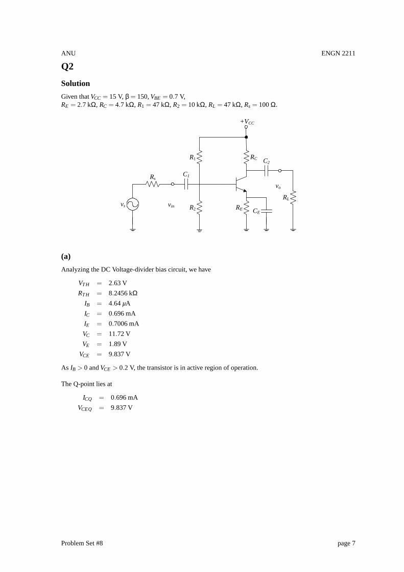
Q2
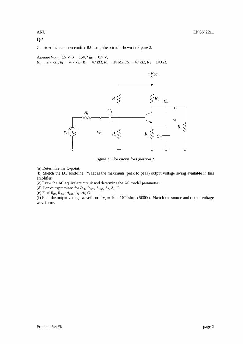
Consider the common-emitter BJT amplifier circuit shown in Figure 2.
AssumeVCC = 15 V, β = 150,VBE = 0.7 V,RE = 2.7 kΩ, RC = 4.7 kΩ, R1 = 47 kΩ, R2 = 10 kΩ, RL = 47 kΩ, Rs = 100Ω.
RC
+VCC
R1
R2 RE
C1
vsCE
C2
Rs
RL
vin
vo
Figure 2: The circuit for Question 2.
(a) Determine the Q-point.(b) Sketch the DC load-line. What is the maximum (peak to peak) output voltage swing available in thisamplifier.(c) Draw the AC equivalent circuit and determine the AC model parameters.(d) Derive expressions forRin, Rout, Avoc, Av, Ai , G.(e) FindRin, Rout, Avoc, Av, Ai , G.(f) Find the output voltage waveform ifvs = 10×10−3sin(2π5000t). Sketch the source and output voltagewaveforms.
Problem Set #8 page 2
ANU ENGN 2211
AUSTRALIAN NATIONAL UNIVERSITYDepartment of Engineering
ENGN 2211 Electronic Circuits and DevicesProblem Set #8 Solution
Q1
Complete Solution
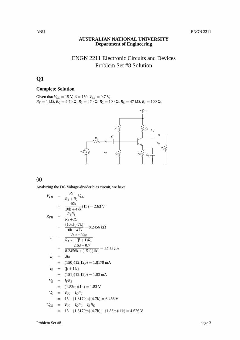
Given thatVCC = 15 V, β = 150,VBE = 0.7 V,RE = 1 kΩ, RC = 4.7 kΩ, R1 = 47 kΩ, R2 = 10 kΩ, RL = 47 kΩ, Rs = 100Ω.
RC
+VCC
R1
R2 RE
C1
vsCE
C2
Rs
RL
vin
vo
(a)
Analyzing the DC Voltage-divider bias circuit, we have
VTH =R2
R1 +R2VCC
=10k
10k+47k(15) = 2.63 V
RTH =R2R1
R1 +R2
=(10k)(47k)10k+47k
= 8.2456 kΩ
IB =VTH −VBE
RTH +(β+1)RE
=2.63−0.7
8.2456k+(151)(1k)= 12.12µA
IC = βIB= (150)(12.12µ) = 1.8179 mA
IE = (β+1)IB= (151)(12.12µ) = 1.83 mA
VE = IERE
= (1.83m)(1k) = 1.83 V
VC = VCC− ICRC
= 15− (1.8179m)(4.7k) = 6.456 V
VCE = VCC− ICRC− IERE
= 15− (1.8179m)(4.7k)− (1.83m)(1k) = 4.626 V
Problem Set #8 page 3
ANU ENGN 2211
As IB > 0 andVCE > 0.2 V, the transistor is in active region of operation.
The Q-point lies at
ICQ = 1.8179 mA
VCEQ = 4.626 V
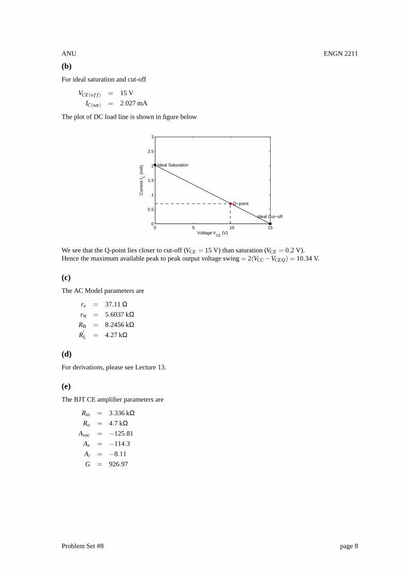
(b)
For ideal cut-off
VCE(o f f) = VCC = 15 V
For ideal saturation
IC(sat) =VCC
RC +RE=
155.7k
= 2.63 mA
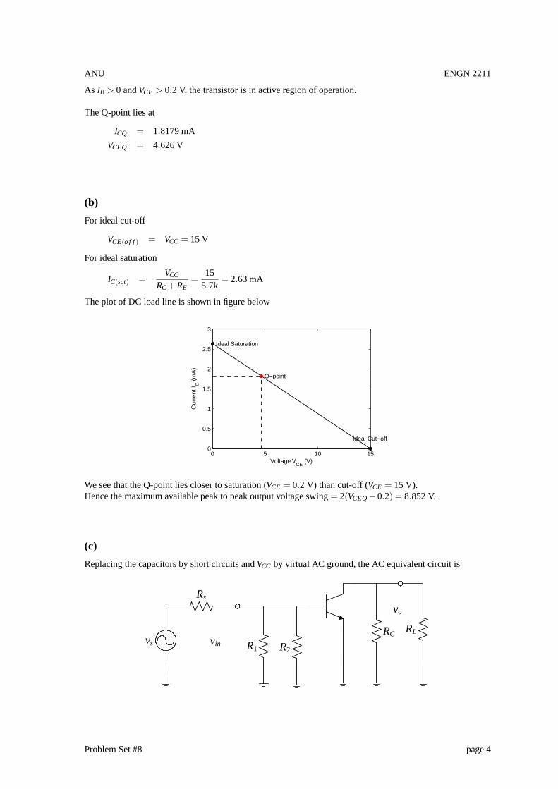
The plot of DC load line is shown in figure below
0 5 10 150
0.5
1
1.5
2
2.5
3
Voltage VCE
(V)
Cur
rent
I C (
mA
)
Q−point
Ideal Saturation
Ideal Cut−off
We see that the Q-point lies closer to saturation (VCE = 0.2 V) than cut-off (VCE = 15 V).Hence the maximum available peak to peak output voltage swing= 2(VCEQ−0.2) = 8.852 V.
(c)
Replacing the capacitors by short circuits andVCC by virtual AC ground, the AC equivalent circuit is
R1vs
Rs
RL
vin
vo
RC
R2
Problem Set #8 page 4
ANU ENGN 2211
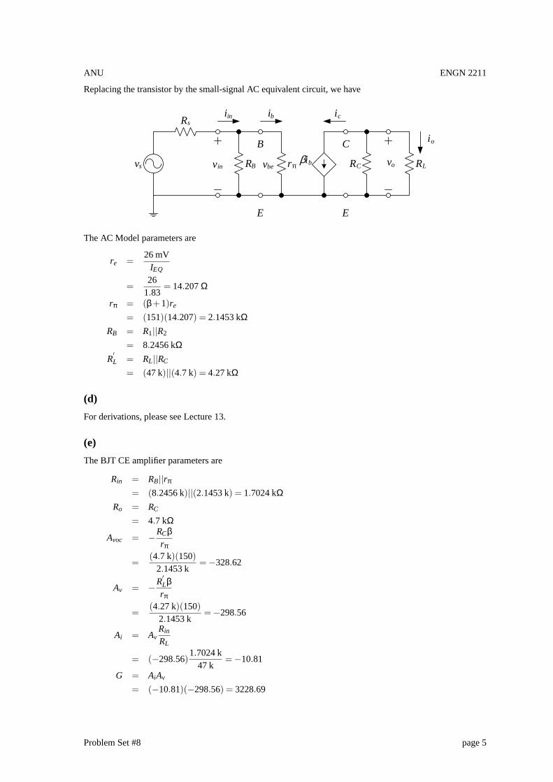
Replacing the transistor by the small-signal AC equivalent circuit, we have
RBvs
Rs
vin vorπ RC RL
B C
E E
βib
ic
io
iin ib
vbe
The AC Model parameters are
re =26 mV
IEQ
=26
1.83= 14.207Ω
rπ = (β+1)re
= (151)(14.207) = 2.1453 kΩRB = R1||R2
= 8.2456 kΩR′L = RL||RC
= (47 k)||(4.7 k) = 4.27 kΩ
(d)
For derivations, please see Lecture 13.
(e)
The BJT CE amplifier parameters are
Rin = RB||rπ
= (8.2456 k)||(2.1453 k) = 1.7024 kΩRo = RC
= 4.7 kΩ
Avoc = −RCβrπ
=(4.7 k)(150)
2.1453 k= −328.62
Av = −R′Lβrπ
=(4.27 k)(150)
2.1453 k= −298.56
Ai = AvRin
RL
= (−298.56)1.7024 k
47 k= −10.81
G = AiAv
= (−10.81)(−298.56) = 3228.69
Problem Set #8 page 5
ANU ENGN 2211
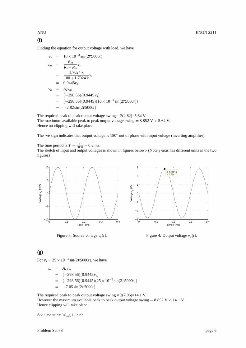
(f)
Finding the equation for output voltage with load, we have
vs = 10×10−3sin(2π5000t)
vin =Rin
Rs+Rinvs
=1.7024 k
100+1.7024 kvs
= 0.9445vs
vo = Avvin
= (−298.56)(0.9445vs)= (−298.56)(0.9445)(10×10−3sin(2π5000t))= −2.82sin(2π5000t)
The required peak to peak output voltage swing = 2(2.82)=5.64 V.The maximum available peak to peak output voltage swing= 8.852 V> 5.64 V.Hence no clipping will take place.
The -ve sign indicates that output voltage is 180 out of phase with input voltage (inverting amplifier).
The time period isT = 15000 = 0.2 ms.
The sketch of input and output voltages is shown in figures below:- (Note y-axis has different units in the twofigures)
0 0.1 0.2 0.3 0.4−10
−5
0
5
10
Vol
tage
vs (
mV
)
Time t (ms)
Figure 3: Source voltagevs(t).
0 0.1 0.2 0.3 0.4−3
−2
−1
0
1
2
3
X: 0.00015Y: 2.824
Vol
tage
vo (
V)
Time t (ms)
Figure 4: Output voltagevo(t).
(g)
Forvs = 25×10−3sin(2π5000t), we have
vo = Avvin
= (−298.56)(0.9445vs)= (−298.56)(0.9445)(25×10−3sin(2π5000t))= −7.05sin(2π5000t)
The required peak to peak output voltage swing = 2(7.05)=14.1 V.However the maximum available peak to peak output voltage swing= 8.852 V< 14.1 V.Hence clipping will take place.
SeeProbSet08_Q1.sch .
Problem Set #8 page 6
ANU ENGN 2211
Q2
Solution
Given thatVCC = 15 V, β = 150,VBE = 0.7 V,RE = 2.7 kΩ, RC = 4.7 kΩ, R1 = 47 kΩ, R2 = 10 kΩ, RL = 47 kΩ, Rs = 100Ω.
RC
+VCC
R1
R2 RE
C1
vsCE
C2
Rs
RL
vin
vo
(a)
Analyzing the DC Voltage-divider bias circuit, we have
VTH = 2.63 V
RTH = 8.2456 kΩIB = 4.64µA
IC = 0.696 mA
IE = 0.7006 mA
VC = 11.72 V
VE = 1.89 V
VCE = 9.837 V
As IB > 0 andVCE > 0.2 V, the transistor is in active region of operation.
The Q-point lies at
ICQ = 0.696 mA
VCEQ = 9.837 V
Problem Set #8 page 7
ANU ENGN 2211
(b)
For ideal saturation and cut-off
VCE(o f f) = 15 V
IC(sat) = 2.027 mA
The plot of DC load line is shown in figure below
0 5 10 150
0.5
1
1.5
2
2.5
3
Voltage VCE
(V)
Cur
rent
I C (
mA
)
Q−point
Ideal Saturation
Ideal Cut−off
We see that the Q-point lies closer to cut-off (VCE = 15 V) than saturation (VCE = 0.2 V).Hence the maximum available peak to peak output voltage swing= 2(VCC−VCEQ) = 10.34 V.
(c)
The AC Model parameters are
re = 37.11Ωrπ = 5.6037 kΩRB = 8.2456 kΩR′L = 4.27 kΩ
(d)
For derivations, please see Lecture 13.
(e)
The BJT CE amplifier parameters are
Rin = 3.336 kΩRo = 4.7 kΩ
Avoc = −125.81
Av = −114.3
Ai = −8.11
G = 926.97
Problem Set #8 page 8
ANU ENGN 2211
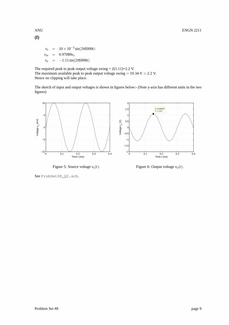
(f)
vs = 10×10−3sin(2π5000t)vin = 0.97089vs
vo = −1.11sin(2π5000t)
The required peak to peak output voltage swing = 2(1.11)=2.2 V.The maximum available peak to peak output voltage swing= 10.34 V > 2.2 V.Hence no clipping will take place.
The sketch of input and output voltages is shown in figures below:- (Note y-axis has different units in the twofigures)
0 0.1 0.2 0.3 0.4−10
−5
0
5
10
Vol
tage
vs (
mV
)
Time t (ms)
Figure 5: Source voltagevs(t).
0 0.1 0.2 0.3 0.4−2
−1.5
−1
−0.5
0
0.5
1
1.5
2
X: 0.00015Y: 1.111
Vol
tage
vo (
V)
Time t (ms)
Figure 6: Output voltagevo(t).
SeeProbSet08_Q2.sch .
Problem Set #8 page 9