engineering internship final report - murdoch...
TRANSCRIPT
MURDOCH UNIVERSITY, PERTH
Engineering Internship
Final Report Regulated Current Source
Wenhan Zhang (Jason)
2014/11/24
This internship was progressed in Red Phase, Melbourne. The project was to create a regulated
current source by using NI LabVIEW, myRIO and H-bridge

Murdoch University Wenhan Zhang
1 / 86
TABLE OF CONTENTS
ABSTRACT .......................................................................................................................................... 7
ACKNOWLEDGEMENTS ..................................................................................................................... 8
1 Introduction .............................................................................................................................. 9
1.1 Red Phase Instruments.............................................................................................. 9
1.2 Internship Project .................................................................................................... 10
1.2.1 Background ..................................................................................................... 10
1.2.2 Aim of the project ........................................................................................... 10
1.2.3 Specification .................................................................................................... 11
1.3 Document Overview................................................................................................ 11
2 Current source ......................................................................................................................... 13
2.1 Background: ............................................................................................................ 13
2.2 Main Circuit Components used ............................................................................... 13
2.3 Overview of the current Source Implementation ................................................... 13
2.3.1 Signal generation ............................................................................................. 14
2.3.2 Current/ Power generation ............................................................................. 14
2.3.3 Feedback Signals ............................................................................................. 14
2.3.4 Protection circuit ............................................................................................. 15
3 Overview of Instrumentation & Software ............................................................................... 16
3.1 Protel 99 SE ............................................................................................................. 16
3.1.1 PCB .................................................................................................................. 16
3.1.2 Protel 99 SE ..................................................................................................... 17
3.2 LabVIEW .................................................................................................................. 18
3.2.1 Introduction..................................................................................................... 18
3.2.2 Benefits of LabVIEW ........................................................................................ 19
3.3 Equipment & Facilities ............................................................................................. 20
3.3.1 Multimeter ...................................................................................................... 20
3.3.2 Power supply ................................................................................................... 20
3.3.3 Assembling tools & equipment ....................................................................... 20
3.4 NI myRIO ................................................................................................................. 21
3.4.1 Introduction to the NI myRIO .......................................................................... 21
3.4.2 Hardware Overview ......................................................................................... 22
3.5 RF Flow .................................................................................................................... 22
4 Overview of main technology ................................................................................................. 23
4.1 H-bridge theory ....................................................................................................... 23
4.1.1 Introduction to the H-bridge circuit ................................................................ 23
4.1.2 H-bridge working principle .............................................................................. 24
4.2 MOSFETs .................................................................................................................. 24
4.2.1 Introduction of MOSFETs ................................................................................. 24
4.2.2 MOSFETs theory .............................................................................................. 25
4.3 Introduction of Field-Programmable Gate Array (FPGA)......................................... 25
4.4 PWM theory ............................................................................................................ 28
4.4.1 Introduction of PWM ...................................................................................... 28

Murdoch University Wenhan Zhang
2 / 86
4.4.2 PWM generation ............................................................................................. 28
4.5 Operational Amplifiers (Op-amps) .......................................................................... 29
4.5.1 Introduction to the Op-Amp............................................................................ 29
4.5.2 Op-amp theory and typical applications ......................................................... 30
4.6 ADC/DAC theory ...................................................................................................... 32
4.6.1 Digital to Analog Conversion ........................................................................... 32
4.6.2 Analog to Digital Conversion ........................................................................... 33
4.7 Low pass filter ......................................................................................................... 35
4.8 LC filter .................................................................................................................... 35
5 Main board design .................................................................................................................. 37
5.1 Digital inputs and AND logic function ..................................................................... 38
5.2 MOSFET driver ......................................................................................................... 39
5.3 Voltage regulator for the MOSFETs driver ............................................................... 41
5.4 H-bridge circuit design ............................................................................................ 41
5.5 Bus current sensor design ....................................................................................... 43
5.6 DC bus voltage feedback circuit .............................................................................. 44
5.7 Output circuit design ............................................................................................... 45
5.8 Amid generator ....................................................................................................... 46
5.9 AC Output current sensor design ............................................................................ 47
6 FPGA code design. ................................................................................................................... 48
6.1 Analog inputs .......................................................................................................... 48
6.2 Input analysis .......................................................................................................... 50
6.3 Sine-wave frequency generator .............................................................................. 50
6.4 Sine-wave generator ............................................................................................... 51
6.5 PWM generation loop ............................................................................................. 52
6.6 PID control for output current................................................................................. 53
6.7 DC PID control loop ................................................................................................. 54
6.8 Protection loop design ............................................................................................ 55
6.9 Output loop design.................................................................................................. 56
6.10 FPGA Front Panel ..................................................................................................... 56
7 Testing, Troubleshooting & Debugging ................................................................................... 58
7.1 Testing the Current Source ...................................................................................... 58
7.2 Open-circuit Test ..................................................................................................... 58
7.3 Testing with the load ............................................................................................... 60
7.4 Testing With Feedback Control Loop ....................................................................... 61
7.5 Troubleshooting & Debugging ................................................................................. 62
7.5.1 Root Cause Analysis ......................................................................................... 62
7.5.2 DC Component Elimination ............................................................................. 64
7.6 Reliability Test.......................................................................................................... 65
7.7 Increasing the Capacitance on the Power Supply ................................................... 65
7.8 Protection Design .................................................................................................... 66
7.8.1 DC Bus Voltage Protection ............................................................................... 66
7.8.2 DC Bus Over-current Protection ...................................................................... 66
7.8.3 Output Voltage Protection .............................................................................. 66

Murdoch University Wenhan Zhang
3 / 86
8 Internship evaluation .............................................................................................................. 67
8.1 Achievements .......................................................................................................... 67
8.2 Enhanced Areas ....................................................................................................... 68
8.2.1 Real-time module ............................................................................................ 68
8.2.2 Remote control module .................................................................................. 68
9 References: ........................................................................................................................... 69
Glossary & Explanation ................................................................................................................... 71
10 Appendices: ..................................................................................................................... 74
1. MOSFETs: ................................................................................................................. 74
2. PWM generation ..................................................................................................... 75
3. Introduction of Digital and Analog signals .............................................................. 76
4. Bus voltage protection ............................................................................................ 77
Schematic diagram: ......................................................................................................................... 83

Murdoch University Wenhan Zhang
4 / 86
List of Table
Table 1: Characteristics of MOSFETs driver _______________________________________________ 41
Table 2: The features of PID control ____________________________________________________ 63
Table 3: Regulated error in different load condition ________________________________________ 65
Table 4: Regulated error measurement __________________________________________________ 79

Murdoch University Wenhan Zhang
5 / 86
List of figure Figure 1:Working structure __________________________________________________________ 14
Figure 2: Complete example circuit on PCB _______________________________________________ 16
Figure 3: Breadboard ________________________________________________________________ 17
Figure 4: Example of schematic circuit design ____________________________________________ 17
Figure 5: PCB layout example _________________________________________________________ 18
Figure 6: LabVIEW workflow __________________________________________________________ 18
Figure 7: Example of a block diagram and corresponding front panel _________________________ 19
Figure 8: DC power supply ____________________________________________________________ 20
Figure 9: NI myRIO-1900 _____________________________________________________________ 21
Figure 10: NI myRIO-1900 Hardware Block Diagram _______________________________________ 22
Figure 11: AN H-bridge connection _____________________________________________________ 23
Figure 12: working principle of H-bridge _________________________________________________ 24
Figure 13: A conceptual generic field-effect transistor ______________________________________ 24
Figure 14: A simple MOSFET structure __________________________________________________ 25
Figure 15: An abstract view of an FPGA _________________________________________________ 26
Figure 16: A typical FPGA mapping flow _________________________________________________ 27
Figure 17: PWM with different duty cycles _______________________________________________ 28
Figure 18: concept of SPWM __________________________________________________________ 28
Figure 19: Standard op-amp symbol ____________________________________________________ 29
Figure 20: inverting op-amp connection _________________________________________________ 31
Figure 21: Noninverting op-amp connection______________________________________________ 31
Figure 22: Op-amp as an inverting amplifier with gain of Rf/Rj _______________________________ 32
Figure 23: A 4-bit DAC with binary-weighted inputs ________________________________________ 33
Figure 24: A 3-bit flash ADC ___________________________________________________________ 34
Figure 25: Sampling of values on an analog waveform for conversion to digital form _____________ 34
Figure 26: resulting digital out puts for sampled values. ____________________________________ 35
Figure 27: LC low pass filter ___________________________________________________________ 35
Figure 28: fifth order low pass LC filter __________________________________________________ 36
Figure 29: Overall schematic diagram of the main board ___________________________________ 37
Figure 30: Main board Overview _______________________________________________________ 38
Figure 31: Digital input connection and PWM control function _______________________________ 39
Figure 32: The MOSFETs driver ________________________________________________________ 39
Figure 33: Typical connection of MOSFETs driver __________________________________________ 40
Figure 34: The voltage regulator connection _____________________________________________ 41
Figure 35: H-bridge schematic diagram _________________________________________________ 42
Figure 36: The connection of current sensor with voltage output _____________________________ 43
Figure 37: DC bus voltage feedback circuit _______________________________________________ 44
Figure 38: Vout1 feedback ____________________________________________________________ 45
Figure 39: Vout2 feedback ____________________________________________________________ 45
Figure 40: The Amid signal generator connection _________________________________________ 46
Figure 41: Output current feedback ____________________________________________________ 47
Figure 42: The output current with an offset _____________________________________________ 47

Murdoch University Wenhan Zhang
6 / 86
Figure 43: Overview of the FPGA code design ____________________________________________ 48
Figure 44: Analog Input ______________________________________________________________ 49
Figure 45: Analysis loop – RMS measurement loop ________________________________________ 50
Figure 46: Sine-wave frequency generator _______________________________________________ 50
Figure 47: Sine-wave generator________________________________________________________ 51
Figure 48: The PWM generation loop ___________________________________________________ 52
Figure 49: Output PID control _________________________________________________________ 53
Figure 50: DC PID control _____________________________________________________________ 54
Figure 51: The protection loop_________________________________________________________ 55
Figure 52: The analog output design ____________________________________________________ 56
Figure 53: FPGA front panel ___________________________________________________________ 56
Figure 54: The aluminum housed axial wire-wound panel mount resistor ______________________ 58
Figure 55: PWM signal from the FPGA __________________________________________________ 59
Figure 56: The output voltage under open-loop condition. __________________________________ 60
Figure 57: Load testing without feedback control _________________________________________ 60
Figure 58: AC output waveform with two sides ___________________________________________ 62
Figure 59: The output oscillating under the feedback control ________________________________ 62
Figure 60: close-loop test with the correct result __________________________________________ 64
Figure 61: The charge in the inversion layer as a function of VD ______________________________ 74
Figure 62: The drain voltage versus drain voltage for an n-channel MOSFET whenG thV V _______ 75
Figure 63: A conceptual circuit for realizing PWM _________________________________________ 76
Figure 64: Voltages in a PWM circuit ___________________________________________________ 76
Figure 65: digital points on an analog curve ______________________________________________ 77
Figure 66: A rough digital reproduction of the analog curve in Figure 65 _______________________ 77
Figure 67: soldering station ___________________________________________________________ 79
Figure 68: Parallel Remover ___________________________________________________________ 80
Figure 69: Wave tip Solder iron ________________________________________________________ 80
Figure 70: Desoldering tool ___________________________________________________________ 81
Figure 71: soldering heating process ____________________________________________________ 82
Figure 72: Schematic diagram 1 _______________________________________________________ 83
Figure 73: Schematic diagram 2 _______________________________________________________ 84
Figure 74: Schematic diagram 3 _______________________________________________________ 85
Figure 75: Schematic diagram 4 _______________________________________________________ 86

Murdoch University Wenhan Zhang
7 / 86
ABSTRACT
Electrical Power Engineering provides a fantastic opportunity for Murdoch University bachelor
students to develop professional knowledge and skills. Until finish all study, they can have a
stronger support and much confident when they going to the real engineering company to work.
Students have the choices to do the research thesis or an internship in a relevant industry
company. The internship is a great experience for students go through the real industry working
and this important experience will help them has a better understanding of the real engineer life.
The company has decided a project with university for the student and during the period, and the
industry supervisor was the major responsible to the student. Student also need report back
regularly the project’s progress and take both of the academic supervisor’s and industry
supervisor’s advice to fix the project.
This report is the final task of the internship program. The internship provides a valuable
experience to work with other electronic engineer for the past four (4) months at Red Phase
Instruments. The purpose of this internship is to test the student how much knowledge they
have mastered until now, and it will performance by a project. The project was to create a
regulated current source by using NI LabVIEW, myRIO and H-bridge circuit. Over this period,
student was doing this project by himself and the industry supervisor was only gives a help if
needed.
This report provided massive information about the project. It was separated to nine (9)
sections and each section was talked about one part of the project design. Student must fully
understand all of knowledge in the project and also must have a strong ability of time
management. There were a lot of challenges in different parts and student has to solve them in
a limit time. The project was all about the electronic work, some of new software and
knowledge were also a big challenge for this project.
After the full testing, the main part of product has been approved with a satisfactory
performance. But there are still few parts that can be improved which include the real-time
module and the remote control PC system.

Murdoch University Wenhan Zhang
8 / 86
ACKNOWLEDGEMENTS
I would like to thank the following people.
First is my family. Thank you for always believing me; it is really important that the power of
belief support me during the past four months. You gave me the power that helps me working
so hard every night when I back to home.
I would thank my academic supervisor Dr. Gregory Crebbin, for his kindly help and essential
advise that makes my project more interesting and makes my report more professional. I would
also like to thank Dr. Gareth Lee for giving me many of useful suggestions on the software design
and also for the FPGA and PID study.
At last, I thank my industry supervisor Mr. Yung Thai. His positive attitude and efficient work
also deep infected me. I like his professional thinking and I really learned a lot when I asked him
a question. Thanks for take a lot of time to supervise me.
Murdoch University, Perth, WA Australia
24th November 2014
Wenhan Zhang
Murdoch University Wenhan Zhang
9 / 86
1 Introduction
This document is a report of the ENG 450 Engineering Internship completely as part of the
Bachelor engineering course.
During an internship, each student is required to work for an industrial company and finish one
engineering project individually. An integrated internship includes tasks such as design to meet
requirements, testing, debugging and documentation. The student is required to observe and
follow safe operating procedures as the work involved may be dangerous (e.g. high voltages or
high power circuits), which is very different to performing laboratory work in university.
Working at Red Phase provided a real engineering environment, where the work was always
carried out in a professional, efficient and enthusiastic manner, which inspired everyone to work
effectively with each other. The internship provided a great opportunity to work with other
engineers and develop plenty of useful and valuable experience. This kind of experience
improved the student’s practical skills and it will be very helpful for their future work.
The 16-week internship was spent working as a member of the products development team on
one project. At first the project plan was to developing a new AC voltage and current signal
source by using a microcontroller to generate a PWM signal to drive an H-Bridge. But taking
into consideration the student’s previous study and also that the company wanted to try some
new ideas; finally, it was decided to use LabVIEW and NI myRIO instead of a microcontroller for
the project. There were also some small changes during the projects progress, such as to restrict
the frequency to 50 Hz and 60 Hz for the signal source, while the initial plan, specified
frequencies selectable over the range 40 Hz to 69Hz. These details are discussed later on.
The major goal was to develop a new AC voltage and current signal source. It included:
Electrical and electronic circuits design
LabVIEW code design
Assembling of the first batch of prototypes and preparing for testing
Debugging and troubleshooting
Testing and verification of the prototypes, against target requirements
The completed signal source will be used internally within the company for further development
work of other instruments and products.
1.1 Red Phase Instruments
Red Phase Instruments has, for the past 36 years, designed and manufactured test equipment to
cater for the needs of the utility supply industry. With some products still in service after 25+
years, Red Phase Instruments has a high reputation of many years’ standing for their good quality
and good relationships with their customers. The services that they provide include
manufacture, maintenance and customization of test instruments. General types of product

Murdoch University Wenhan Zhang
10 / 86
include the following:1
Instrumentation Equipment:
Current and potential transformer testing offline, CT / CVT testing, Burden testing.
Installation & Commissioning (for utilities contractors and educational institutions) :
Watt and phase angle meters, Ammeters.
Partial Discharge (Statistical and precedence detection)
Meter Testing (Poly-phase field meters, Bench and outline meters) :
KWh Meter testing with / without load.
Phantom Loads:
Linear and adjustable phase phantom load.
Earth testing Equipment:
1.5KVA, 2KVA, 8KVA earth injection system; lighting impulse tester.
1.2 Internship Project
1.2.1 Background
Red Phase’s product development team wanted to create a current source for their customers as
well as for internal use. It was considered more cost effective to develop this current source
rather than purchase a commercial product. The new current source will be designed to be
sufficiently flexible as to meet specific customer and internal requirements for development
purposes. Some of the flexibility is provided by using LabVIEW software and NI myRIO
hardware to cater for future needs.
1.2.2 Aim of the project
The aim of the project was to make a reliable current source that will output a controlled
regulated AC current capable of 40 watts power output with a variable frequency. A full system
including the software program, signal generator, power converter, feedback circuit, and a
protection circuit were required. The circuits needed to be built and tested. Some of skills,
technology and knowledge required to complete the main objectives in this project were:
1. FPGA working principle;
2. H-Bridge working principle;
3. LabVIEW software
4. PWM theory;
5. Op-amp theory;
6. DAC/ ADC theory;
7. L-C filter theory;
8. Power electronics: MOSFETs theory, etc…
These are just some of the most important knowledge and, other basic knowledge such as I/O
interface buses, binary numbers, sign numbers, floating-point numbers also needed to be fully
1 Red Phase Instruments. Product Catalogue 2013-14.
Murdoch University Wenhan Zhang
11 / 86
understood; they are described in the following sections.
After completing this project, the author will have understood the various stages of the product
development process.
1.2.3 Specification
The final specifications of the current source are:
Frequency range: 50 Hz/ 60 Hz
Amplitude (rms) current output range: 0 – 3.7A
Output power: maximum 50W
Regulation error: maximum 2% between the full load condition and output short-circuited
condition
Protection against fault scenarios:
Open-circuit protection
DC bus current
DC bus voltage protection
Working well under the short-circuit condition.
1.3 Document Overview
This final report has twelve (12) chapters, and each chapter in summarized below.
Chapter 1: an introduction of the internship company, project and also of the current source.
Chapter 2: an overview of the project and an introduction to the current source. This chapter
describes the project with some sections on background, main circuit components used,
overview of the current source implementation.
Chapter 3: an overview of the instrumentation, tools and software. This chapter covers all the
tools I needed during my design, making and testing period, such as the soldering tool,
oscilloscope, and screwdriver, etc. In addition, it also contains an overview of LabVIEW, which is
the programmable software.
Chapter 4: the main technology worked in the NI myRIO mentioned in this chapter. A review of
its knowledge is necessary to better understand the project. Some knowledge about the
hardware operation, like the H-bridge theory, and some knowledge about the software and signal
generation, are also provided in this chapter.
Chapter 5: an overview about the main board design breaks down the information to very
detailed separate sections.
Chapter 6: the software design was use the LabVIEW to create the FPGA code. The functions of
the FPGA code cove signal generation, signal analysis, and signal output, such as the PWM
generation, PID control and protection features.
Chapter 7: testing, troubleshooting and debugging were the last steps in the project. In this
project, some major problems encountered during the testing are discovered. The reasons for
each problem are identified and correspondingly, solutions are provided
Chapter 8: the project evaluation includes the achievements, and areas of possible enhancement
area. The achievements a feature and specifications of the regulated current source. The

Murdoch University Wenhan Zhang
12 / 86
enhanced area has two (2) points that can be improved for the project in the future.

Murdoch University Wenhan Zhang
13 / 86
2 Current source
2.1 Background:
A current source is a very common device in electrical/electronic circuits. It is a circuit that
plays an important role in the two fields of electrical and electronic engineering. “Current
sources are created by combining diodes, resistors, and transistors (BJTs or FETs). They can also
be created at the circuit board level by using discretes, matched pairs, transistor arrays, or by
combining op amps with precision voltage references.”2
An ideal current source can output any current independent of voltage or load conditions.
However, a real physical current source performance is always limited by its actual
implementation. It can be said that an ideal current source is a mathematical model, and that is
a real current source can only approximate its ideal performance within physical limits.
2.2 Main Circuit Components used
1. H-Bridge Circuit
An H-Bridge circuit is a simple circuit model composed of four MOSFETs and several
low-pass filters. It is responsible for generate the AC wave form.
2. Operational Amplifier (Op-amp)
Op-amp is one of the most important and powerful electronic devices. It can be used to do
some mathematical operations like addition, subtraction and multiplication by some values.
“In addition, op-amps can be used to produce comparators, waveform generators, current
sources, voltage regulators, filters and many other signal processing functions.”3
3. MOSFETs driver (high and low side driver)
As the name says, it is a specific device used to drive (or switch) the MOSFETs on and off.
4. Voltage regulator
A voltage regulator is a constant voltage source. It adjusts its internal resistance when the
load resistance is changed to provide a constant output voltage.
5. Resistors, capacitors, inductors and diodes.
These things are very basic components used in the circuit, some played an instrumental
role in the output filtering, and some are the part of a higher level circuit.
2.3 Overview of the current Source Implementation
The current source was implemented using four main parts: signal generation, current/ power
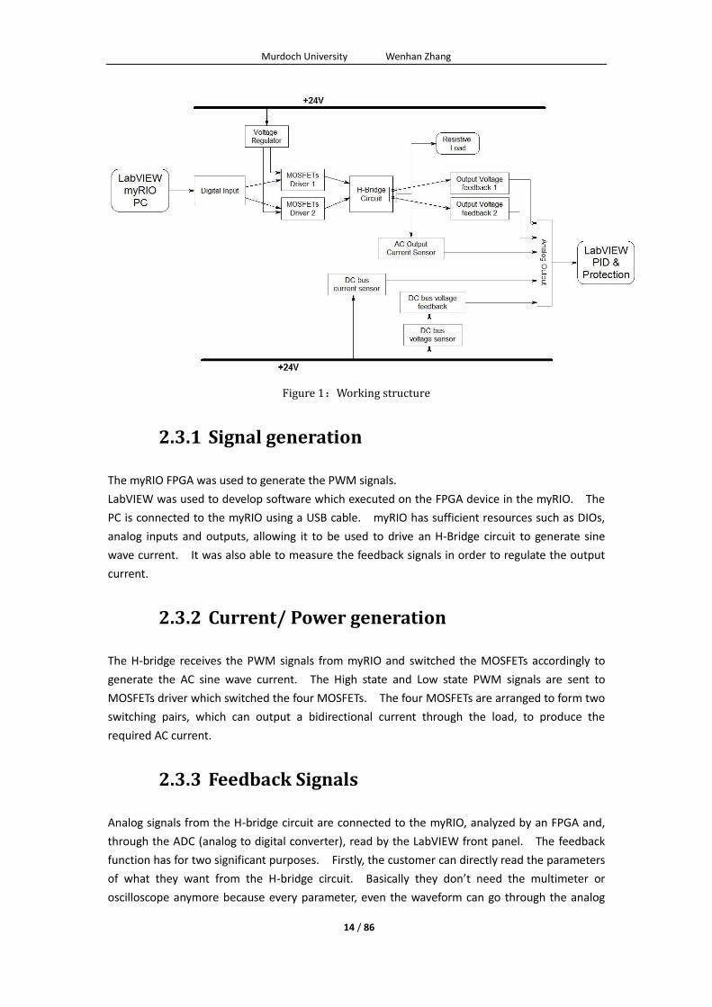
generation, feedback and protection. The working structure is shown in Figure 1.
2 Linden T. Harrison. “An introduction to current sources“, in Current sources & voltage references. 2005, Chapter 2.
3 Richard R. Spencer, “Operational Amplifiers”, in Mohammed S. Ghausi. Introduction Electronic Circuit Design. 2001, Chapter 5.
Murdoch University Wenhan Zhang
14 / 86
Figure 1:Working structure
2.3.1 Signal generation
The myRIO FPGA was used to generate the PWM signals.
LabVIEW was used to develop software which executed on the FPGA device in the myRIO. The
PC is connected to the myRIO using a USB cable. myRIO has sufficient resources such as DIOs,
analog inputs and outputs, allowing it to be used to drive an H-Bridge circuit to generate sine
wave current. It was also able to measure the feedback signals in order to regulate the output
current.
2.3.2 Current/ Power generation
The H-bridge receives the PWM signals from myRIO and switched the MOSFETs accordingly to
generate the AC sine wave current. The High state and Low state PWM signals are sent to
MOSFETs driver which switched the four MOSFETs. The four MOSFETs are arranged to form two
switching pairs, which can output a bidirectional current through the load, to produce the
required AC current.
2.3.3 Feedback Signals
Analog signals from the H-bridge circuit are connected to the myRIO, analyzed by an FPGA and,
through the ADC (analog to digital converter), read by the LabVIEW front panel. The feedback
function has for two significant purposes. Firstly, the customer can directly read the parameters
of what they want from the H-bridge circuit. Basically they don’t need the multimeter or
oscilloscope anymore because every parameter, even the waveform can go through the analog

Murdoch University Wenhan Zhang
15 / 86
inputs of the FPGA and be read on the LabVIEW user interface panel. In addition, the feedback
signal is also can be used for current regulation and circuit protection. When an error or fault
occurs, after some calculations, the FPGA can detect the fault condition and by using the fault
protection program, it can shut down the H-bridge circuit to protect the whole system.
2.3.4 Protection circuit
The protection circuit has two parts. One is embedded in the H-bridge circuit; it is actually a
kind of sensor to read the current or voltage value and send the value to myRIO for analysis.
The other part is an analysis program written in LabVIEW program. This part compares between
the output signals with threshold values. When an output(s) is greater (or lower) than a
threshold value, it will assert a fault condition and trip the circuit.
Murdoch University Wenhan Zhang
16 / 86
3 Overview of Instrumentation &
Software
The list of tools and instrumentation used to complete this project are described in this chapter.
3.1 Protel 99 SE
3.1.1 PCB
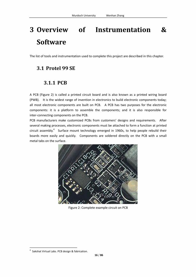
A PCB (Figure 2) is called a printed circuit board and is also known as a printed wiring board
(PWB). It is the widest range of invention in electronics to build electronic components today;
all most electronic components are built on PCB. A PCB has two purposes for the electronic
components: it is a platform to assemble the components; and it is also responsible for
inter-connecting components on the PCB.
PCB manufacturers make customized PCBs from customers’ designs and requirements. After
several making processes, electronic components must be attached to form a function at printed
circuit assembly.4 Surface mount technology emerged in 1960s, to help people rebuild their
boards more easily and quickly. Components are soldered directly on the PCB with a small
metal tabs on the surface.
Figure 2: Complete example circuit on PCB
4 Sakshat Virtual Labs. PCB design & fabrication.

Murdoch University Wenhan Zhang
17 / 86
Figure 3: Breadboard5
Breadboard (Figure 3): This is a simple way for laboratory to do some labs testing quickly.
Designer can just place the component leads through the holes to complete their circuit;
it is also possible to reuse the components. Therefore, Breadboards are always popular
in electronic design work
3.1.2 Protel 99 SE
Protel 99 SE is one of the major software tools for electronic circuit designers. It has two main
parts: schematic design (Figure 4) and PCB layout design (Figure 5).
A schematic diagram shows the connection in a circuit that is standardized and academic.
It is a way of communication to other engineers to show exactly the circuit function and it is
also a simple way for engineers to check their work. The schematic diagram is the basic
and main method for electrical and electronic engineer to develop their work, an example is
shown in Figure 4.
Figure 4: Example of schematic circuit design
5 Sakshat Virtual Labs. PCB design & fabrication.
Murdoch University Wenhan Zhang
18 / 86
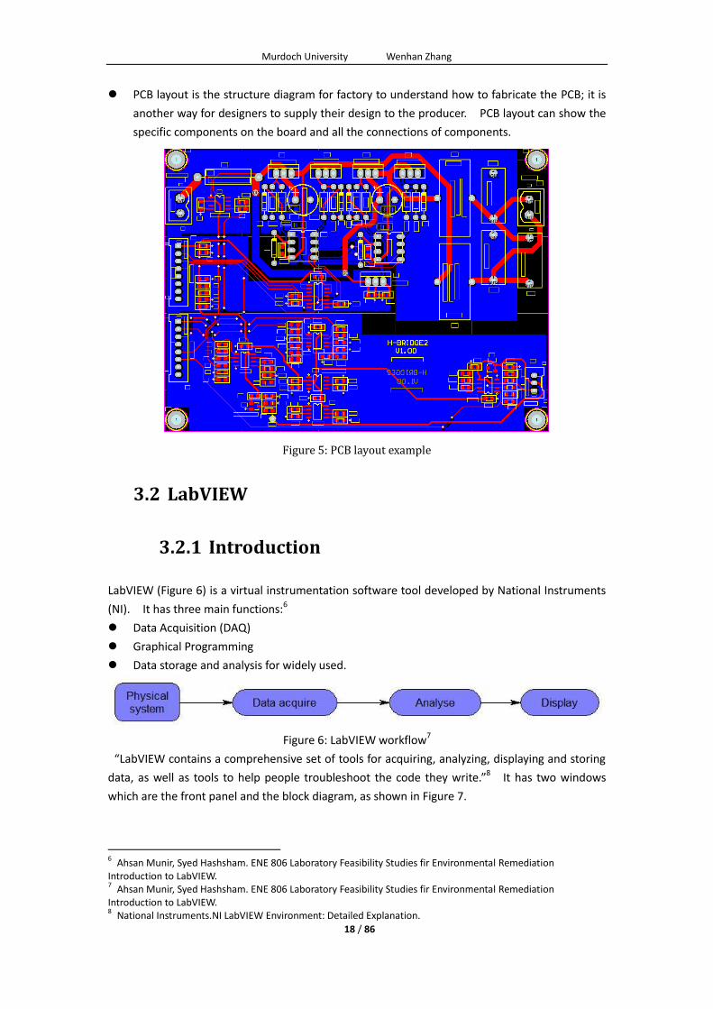
PCB layout is the structure diagram for factory to understand how to fabricate the PCB; it is
another way for designers to supply their design to the producer. PCB layout can show the
specific components on the board and all the connections of components.
Figure 5: PCB layout example
3.2 LabVIEW
3.2.1 Introduction
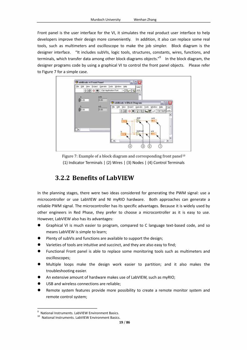
LabVIEW (Figure 6) is a virtual instrumentation software tool developed by National Instruments
(NI). It has three main functions:6
Data Acquisition (DAQ)
Graphical Programming
Data storage and analysis for widely used.
Figure 6: LabVIEW workflow7
“LabVIEW contains a comprehensive set of tools for acquiring, analyzing, displaying and storing
data, as well as tools to help people troubleshoot the code they write.”8 It has two windows
which are the front panel and the block diagram, as shown in Figure 7.
6 Ahsan Munir, Syed Hashsham. ENE 806 Laboratory Feasibility Studies fir Environmental Remediation
Introduction to LabVIEW. 7 Ahsan Munir, Syed Hashsham. ENE 806 Laboratory Feasibility Studies fir Environmental Remediation
Introduction to LabVIEW. 8 National Instruments.NI LabVIEW Environment: Detailed Explanation.
Murdoch University Wenhan Zhang
19 / 86
Front panel is the user interface for the VI, it simulates the real product user interface to help
developers improve their design more conveniently. In addition, it also can replace some real
tools, such as multimeters and oscilloscope to make the job simpler. Block diagram is the
designer interface. “It includes subVIs, logic tools, structures, constants, wires, functions, and
terminals, which transfer data among other block diagrams objects.”9 In the block diagram, the
designer programs code by using a graphical VI to control the front panel objects. Please refer
to Figure 7 for a simple case.
Figure 7: Example of a block diagram and corresponding front panel10
(1) Indicator Terminals | (2) Wires | (3) Nodes | (4) Control Terminals
3.2.2 Benefits of LabVIEW
In the planning stages, there were two ideas considered for generating the PWM signal: use a
microcontroller or use LabVIEW and NI myRIO hardware. Both approaches can generate a
reliable PWM signal. The microcontroller has its specific advantages. Because it is widely used by
other engineers in Red Phase, they prefer to choose a microcontroller as it is easy to use.
However, LabVIEW also has its advantages:
Graphical VI is much easier to program, compared to C language text-based code, and so
means LabVIEW is simple to learn;
Plenty of subVIs and functions are available to support the design;
Varieties of tools are intuitive and succinct, and they are also easy to find;
Functional Front panel is able to replace some monitoring tools such as multimeters and
oscilloscopes;
Multiple loops make the design work easier to partition; and it also makes the
troubleshooting easier.
An extensive amount of hardware makes use of LabVIEW, such as myRIO;
USB and wireless connections are reliable;
Remote system features provide more possibility to create a remote monitor system and
remote control system;
9 National Instruments. LabVIEW Environment Basics.
10 National Instruments. LabVIEW Environment Basics.

Murdoch University Wenhan Zhang
20 / 86
Based on these advantages, NI LabVIEW and myRIO are adopted for project use.
3.3 Equipment & Facilities
3.3.1 Multimeter
The multimeter is useful when the experimenter wants to measure current, voltage or it is also
can be used for short-circuit checkup. In this project, it was used to check the condition of the
MOSFETs because during protection design, many MOSFETs were damaged under short-circuit
conditions. When a huge injection current passes through the MOSFETs, it can result in
permanent damage due to too much energy dissipated within the device. The multimeter can
measure the resistance between the sources and drain terminals. If the resistance is very low
(normally is around 5K Ohms to 1M Ohms), then that means the MOSFET is damaged needs to be
replaced.
3.3.2 Power supply
Virtually every electronic product requires some kind of power supply. There are two basic types
of power supplies: AC power supply and DC power supply. Many energy-consuming equipment
and applications operate on DC, and that also includes our H-bridge circuit. The general way to
create a DC power supply like they are shown in Figure 8 is to use an AC-DC converter and DC-DC
converter to produce a low voltage DC supply.
Figure 8: DC power supply
3.3.3 Assembling tools & equipment
Some tools are also necessary during the H-bridge board assembling:
Murdoch University Wenhan Zhang
21 / 86
Screwdriver (screws; nuts);
Tweezers;
Wire stripper;
Pliers;
Side cutters;
Wire twister ;
Heat sink:
To cool down the load when operating the system;
Tape;
Heat shrink:
To isolate the wires from each other;
Resistors, capacitors, inductors, op-amps, MOSFETs, diodes and etc.
3.4 NI myRIO
3.4.1 Introduction to the NI myRIO
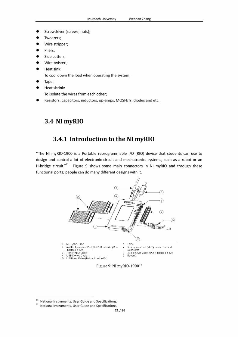
“The NI myRIO-1900 is a Portable reprogrammable I/O (RIO) device that students can use to
design and control a lot of electronic circuit and mechatronics systems, such as a robot or an
H-bridge circuit.”11 Figure 9 shows some main connectors in NI myRIO and through these
functional ports; people can do many different designs with it.
Figure 9: NI myRIO-190012
11
National Instruments. User Guide and Specifications. 12
National Instruments. User Guide and Specifications.
Murdoch University Wenhan Zhang
22 / 86
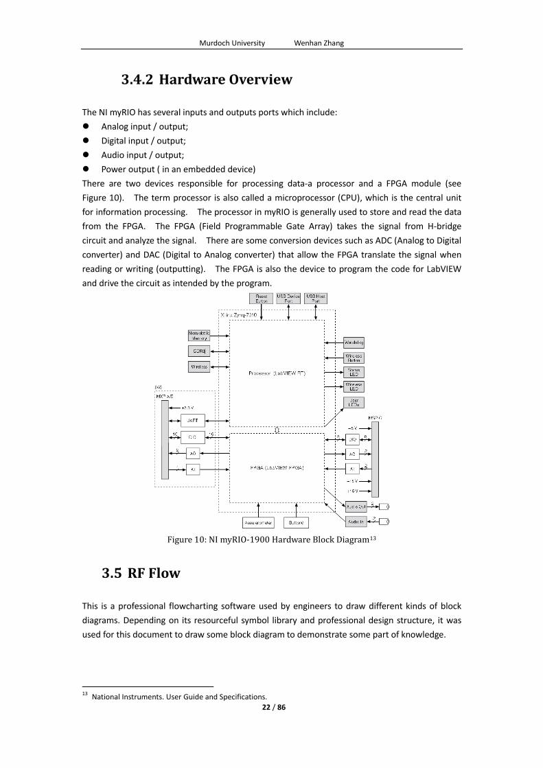
3.4.2 Hardware Overview
The NI myRIO has several inputs and outputs ports which include:
Analog input / output;
Digital input / output;
Audio input / output;
Power output ( in an embedded device)
There are two devices responsible for processing data-a processor and a FPGA module (see
Figure 10). The term processor is also called a microprocessor (CPU), which is the central unit
for information processing. The processor in myRIO is generally used to store and read the data
from the FPGA. The FPGA (Field Programmable Gate Array) takes the signal from H-bridge
circuit and analyze the signal. There are some conversion devices such as ADC (Analog to Digital
converter) and DAC (Digital to Analog converter) that allow the FPGA translate the signal when
reading or writing (outputting). The FPGA is also the device to program the code for LabVIEW
and drive the circuit as intended by the program.
Figure 10: NI myRIO-1900 Hardware Block Diagram13
3.5 RF Flow
This is a professional flowcharting software used by engineers to draw different kinds of block
diagrams. Depending on its resourceful symbol library and professional design structure, it was
used for this document to draw some block diagram to demonstrate some part of knowledge.
13
National Instruments. User Guide and Specifications.
Murdoch University Wenhan Zhang
23 / 86
4 Overview of main technology
4.1 H-bridge theory
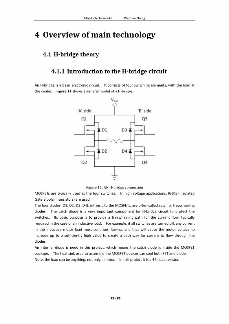
4.1.1 Introduction to the H-bridge circuit
An H-bridge is a basic electronic circuit. It consists of four switching elements, with the load at
the center. Figure 11 shows a general model of a H-bridge.
Figure 11: AN H-bridge connection
MOSFETs are typically used as the four switches. In high voltage applications, IGBTs (Insulated
Gate Bipolar Transistors) are used.
The four diodes (D1, D2, D3, D4), intrinsic to the MOSFETs, are often called catch or freewheeling
diodes. The catch diode is a very important component for H-bridge circuit to protect the
switches. Its basic purpose is to provide a freewheeling path for the current flow, typically
required in the case of an inductive load. For example, if all switches are turned off, any current
in the inductive motor load must continue flowing, and that will cause the motor voltage to
increase up to a sufficiently high value to create a path way for current to flow through the
diodes.
An internal diode is need in this project, which means the catch diode is inside the MOSFET
package. The heat sink used to assemble the MOSFET devices can cool both FET and diode.
Note, the load can be anything, not only a motor. In this project it is a 4Ωload resistor.
Murdoch University Wenhan Zhang
24 / 86
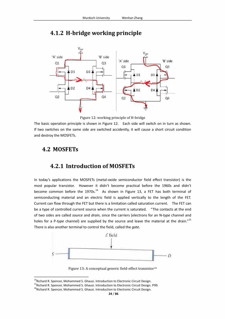
4.1.2 H-bridge working principle
Figure 12: working principle of H-bridge
The basic operation principle is shown in Figure 12. Each side will switch on in turn as shown.
If two switches on the same side are switched accidently, it will cause a short circuit condition
and destroy the MOSFETs.
4.2 MOSFETs
4.2.1 Introduction of MOSFETs
In today’s applications the MOSFETs (metal-oxide semiconductor field effect transistor) is the
most popular transistor. However it didn’t become practical before the 1960s and didn’t
become common before the 1970s.14 As shown in Figure 13, a FET has both terminal of
semiconducting material and an electric field is applied vertically to the length of the FET.
Current can flow through the FET but there is a limitation called saturation current. The FET can
be a type of controlled current source when the current is saturated. “The contacts at the end
of two sides are called source and drain, since the carriers (electrons for an N-type channel and
holes for a P-type channel) are supplied by the source and leave the material at the drain.”15
There is also another terminal to control the field, called the gate.
Figure 13: A conceptual generic field-effect transistor16
14
Richard R. Spencer, Mohammed S. Ghausi. Introduction to Electronic Circuit Design. 15
Richard R. Spencer, Mohammed S. Ghausi. Introduction to Electronic Circuit Design. P99. 16
Richard R. Spencer, Mohammed S. Ghausi. Introduction to Electronic Circuit Design.

Murdoch University Wenhan Zhang
25 / 86
4.2.2 MOSFETs theory
Figure 14 shows a simplified MOSFET construction drawing. The device is based on a p-type
silicon base and two heavily-doped n-type regions for the drain and source. The gate material is
heavily doped polysilicon and is separated from the silicon by an oxide layer.
Figure 14: A simple MOSFET structure17
The VG is a control source. When it less than zero (0), the silicon surface attracts the holes to
the surface, and there is no current flow because for both of the source-to-bulk pn junction and
the drain-to-bulk pn junction are reverse biased. In turn, if the gate voltage 0GV , then the
holes will be pushed to the gate; and mobile electrons can through the holes to be a current flow.
In this condition, the bulk material will convert from p-type to n-type, and the layer of mobile
electrons is forms an inversion layer. Another basic parameter is threshold voltage is defined
the voltage when the mobile electrons density is equal to the bulk holes density.
4.3 Introduction of Field-Programmable Gate Array
(FPGA)
In the past decades, the field-programmable gate array went through a glorious path. It
provides numerous benefits to the designer that the traditional devices such as application
specific integrated circuits cannot achieve. The FPGA perfectly blends the benefits of hardware
and the advantages of software.
17
Richard R. Spencer, Mohammed S. Ghausi. Introduction to Electronic Circuit Design. P100.

Murdoch University Wenhan Zhang
26 / 86
Figure 15: An abstract view of an FPGA18
Figure 15 shows the abstract internal structure of an FPGA, which is composed of many small
logic blocks. Each logic block consists of some logic components such as op-amps or flip-flops
for processing logic calculations. Each block is simple and generally allows only a few inputs, yet
the FPGA offers a huge number of combinations that can be built on a chip. Therefore, the
FPGA can be a powerful device for electronics. By programming the code for FPGA, it can
perform any type of analysis functions that the customer desire.
The FPGA is easy to use and can be applied in many applications. Designers use different tools
to develop FPGA code written in a hardware description language, such as VHDL or Verilog HDL.
Designing the FPGA code generally needs the following steps: “Logic synthesis converts high-level
logic constructs and behavioral code into logic gates, followed by technology mapping to
separate the gates into groupings that best match the FPGA's logic resources.”19 Software is
usually written as a sequential program for the FPGA to achieve the functional objectives. A
text-based coding is a common tool used, but in this project, the LabVIEW graphical-based tool
will be used.
18
Scott Hauck, AbdreDehon. Reconfigurable Computing - The Theory and Practice of FPGA-Based Computation. 19
Scott Hauck, AbdreDehon. Reconfigurable Computing - The Theory and Practice of FPGA-Based Computation.
Murdoch University Wenhan Zhang
27 / 86
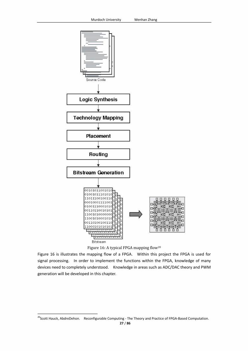
Figure 16: A typical FPGA mapping flow20
Figure 16 is illustrates the mapping flow of a FPGA. Within this project the FPGA is used for
signal processing. In order to implement the functions within the FPGA, knowledge of many
devices need to completely understood. Knowledge in areas such as ADC/DAC theory and PWM
generation will be developed in this chapter.
20
Scott Hauck, AbdreDehon. Reconfigurable Computing - The Theory and Practice of FPGA-Based Computation.
Murdoch University Wenhan Zhang
28 / 86
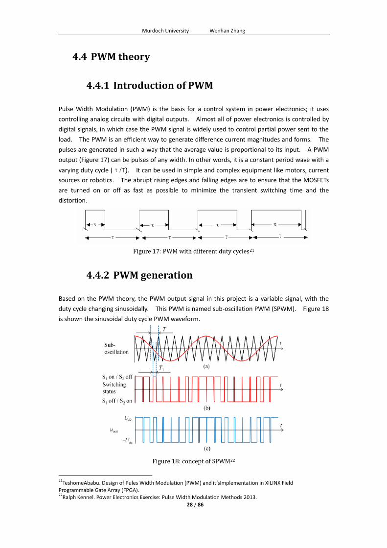
4.4 PWM theory
4.4.1 Introduction of PWM
Pulse Width Modulation (PWM) is the basis for a control system in power electronics; it uses
controlling analog circuits with digital outputs. Almost all of power electronics is controlled by
digital signals, in which case the PWM signal is widely used to control partial power sent to the
load. The PWM is an efficient way to generate difference current magnitudes and forms. The
pulses are generated in such a way that the average value is proportional to its input. A PWM
output (Figure 17) can be pulses of any width. In other words, it is a constant period wave with a
varying duty cycle (τ/T). It can be used in simple and complex equipment like motors, current
sources or robotics. The abrupt rising edges and falling edges are to ensure that the MOSFETs
are turned on or off as fast as possible to minimize the transient switching time and the
distortion.
Figure 17: PWM with different duty cycles21
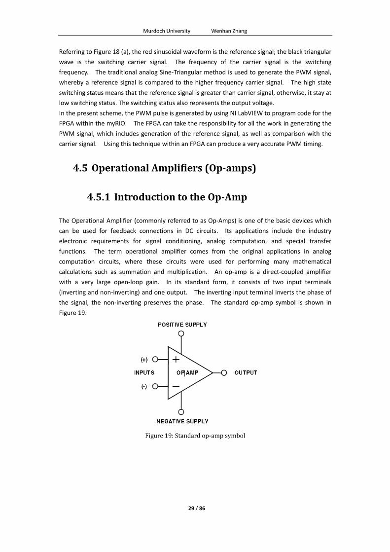
4.4.2 PWM generation
Based on the PWM theory, the PWM output signal in this project is a variable signal, with the
duty cycle changing sinusoidally. This PWM is named sub-oscillation PWM (SPWM). Figure 18
is shown the sinusoidal duty cycle PWM waveform.
Figure 18: concept of SPWM22
21
TeshomeAbabu. Design of Pules Width Modulation (PWM) and it’sImplementation in XILINX Field Programmable Gate Array (FPGA). 22
Ralph Kennel. Power Electronics Exercise: Pulse Width Modulation Methods 2013.
Murdoch University Wenhan Zhang
29 / 86
Referring to Figure 18 (a), the red sinusoidal waveform is the reference signal; the black triangular
wave is the switching carrier signal. The frequency of the carrier signal is the switching
frequency. The traditional analog Sine-Triangular method is used to generate the PWM signal,
whereby a reference signal is compared to the higher frequency carrier signal. The high state
switching status means that the reference signal is greater than carrier signal, otherwise, it stay at
low switching status. The switching status also represents the output voltage.
In the present scheme, the PWM pulse is generated by using NI LabVIEW to program code for the
FPGA within the myRIO. The FPGA can take the responsibility for all the work in generating the
PWM signal, which includes generation of the reference signal, as well as comparison with the
carrier signal. Using this technique within an FPGA can produce a very accurate PWM timing.
4.5 Operational Amplifiers (Op-amps)
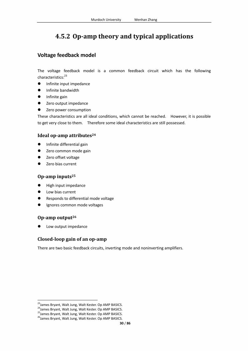
4.5.1 Introduction to the Op-Amp
The Operational Amplifier (commonly referred to as Op-Amps) is one of the basic devices which
can be used for feedback connections in DC circuits. Its applications include the industry
electronic requirements for signal conditioning, analog computation, and special transfer
functions. The term operational amplifier comes from the original applications in analog
computation circuits, where these circuits were used for performing many mathematical
calculations such as summation and multiplication. An op-amp is a direct-coupled amplifier
with a very large open-loop gain. In its standard form, it consists of two input terminals
(inverting and non-inverting) and one output. The inverting input terminal inverts the phase of
the signal, the non-inverting preserves the phase. The standard op-amp symbol is shown in
Figure 19.
Figure 19: Standard op-amp symbol
Murdoch University Wenhan Zhang
30 / 86
4.5.2 Op-amp theory and typical applications
Voltage feedback model
The voltage feedback model is a common feedback circuit which has the following
characteristics:23
Infinite input impedance
Infinite bandwidth
Infinite gain
Zero output impedance
Zero power consumption
These characteristics are all ideal conditions, which cannot be reached. However, it is possible
to get very close to them. Therefore some ideal characteristics are still possessed.
Ideal op-amp attributes24
Infinite differential gain
Zero common mode gain
Zero offset voltage
Zero bias current
Op-amp inputs25
High input impedance
Low bias current
Responds to differential mode voltage
Ignores common mode voltages
Op-amp output26
Low output impedance
Closed-loop gain of an op-amp
There are two basic feedback circuits, inverting mode and noninverting amplifiers.
23
James Bryant, Walt Jung, Walt Kester. Op AMP BASICS. 24
James Bryant, Walt Jung, Walt Kester. Op AMP BASICS. 25
James Bryant, Walt Jung, Walt Kester. Op AMP BASICS. 26
James Bryant, Walt Jung, Walt Kester. Op AMP BASICS.

Murdoch University Wenhan Zhang
31 / 86
Figure 20: inverting op-amp connection27
Precircuit for an inverting op-amp is shown in Figure 20. It has differential input and an output
terminal. The input terminals have a mark “+”as the noninverting input, and “-”which is
inverting input. The output signal has an equation
2
1
( )o a b i
ZV a V V V
Z (1)
The value of a is the open-loop gain of the amplifier. The power supply is also necessary for
the op-amp. The closed loop function can be calculated by the following equation, and by using
an intermediate parameter Va to present:
o aV aV (2)
Figure 21: Noninverting op-amp connection
The noninverting op-amp is another application where the output voltage is not modified by the
loading of the Z1-Z2. The voltage Vα in inverting connection can be calculated by equation (3)
which is shown below
2 1
1 2 1 2
a i o
Z ZV V V
Z Z Z Z
(3)
Combining equation (2) and (3), and after some manipulation, the ration of output voltage to
input voltage is given by:
27
James K. Roberge, Kent H. Lundberg. Operational Amplifiers:Theory and Practice. Second Edition,
Version 1.8.1
Murdoch University Wenhan Zhang
32 / 86
2
1 2
1
1 2
1
o
i
Za
V Z Z
ZVaZ Z
(4)
4.6 ADC/DAC theory
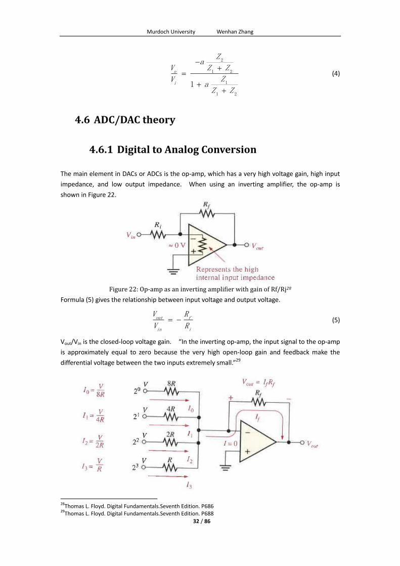
4.6.1 Digital to Analog Conversion
The main element in DACs or ADCs is the op-amp, which has a very high voltage gain, high input
impedance, and low output impedance. When using an inverting amplifier, the op-amp is
shown in Figure 22.
Figure 22: Op-amp as an inverting amplifier with gain of Rf/Rj28
Formula (5) gives the relationship between input voltage and output voltage.
out f
in i
V R
V R (5)
Vout/Vin is the closed-loop voltage gain. “In the inverting op-amp, the input signal to the op-amp
is approximately equal to zero because the very high open-loop gain and feedback make the
differential voltage between the two inputs extremely small.”29
28
Thomas L. Floyd. Digital Fundamentals.Seventh Edition. P686 29
Thomas L. Floyd. Digital Fundamentals.Seventh Edition. P688
Murdoch University Wenhan Zhang
33 / 86
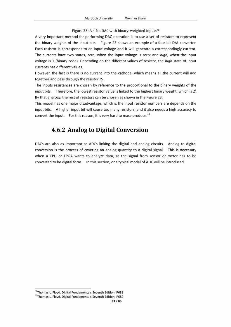
Figure 23: A 4-bit DAC with binary-weighted inputs30
A very important method for performing DAC operation is to use a set of resistors to represent
the binary weights of the input bits. Figure 23 shows an example of a four-bit D/A converter.
Each resistor is corresponds to an input voltage and it will generate a correspondingly current.
The currents have two states, zero, when the input voltage is zero; and high, when the input
voltage is 1 (binary code). Depending on the different values of resistor, the high state of input
currents has different values.
However, the fact is there is no current into the cathode, which means all the current will add
together and pass through the resistor Rf.
The inputs resistances are chosen by reference to the proportional to the binary weights of the
input bits. Therefore, the lowest resistor value is linked to the highest binary weight, which is 23.
By that analogy, the rest of resistors can be chosen as shown in the Figure 23.
This model has one major disadvantage, which is the input resistor numbers are depends on the
input bits. A higher input bit will cause too many resistors, and it also needs a high accuracy to
convert the input. For this reason, it is very hard to mass-produce.31
4.6.2 Analog to Digital Conversion
DACs are also as important as ADCs linking the digital and analog circuits. Analog to digital
conversion is the process of covering an analog quantity to a digital signal. This is necessary
when a CPU or FPGA wants to analyze data, as the signal from sensor or meter has to be
converted to be digital form. In this section, one typical model of ADC will be introduced.
30
Thomas L. Floyd. Digital Fundamentals.Seventh Edition. P688 31
Thomas L. Floyd. Digital Fundamentals.Seventh Edition. P689
Murdoch University Wenhan Zhang
34 / 86
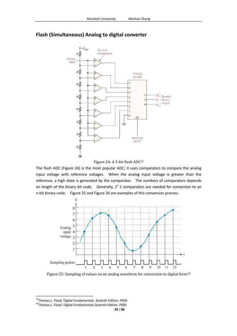
Flash (Simultaneous) Analog to digital converter
Figure 24: A 3-bit flash ADC32
The flash ADC (Figure 24) is the most popular ADC; it uses comparators to compare the analog
input voltage with reference voltages. When the analog input voltage is greater than the
reference, a high state is generated by the comparator. The numbers of comparators depends
on length of the binary bit code. Generally, 2n-1 comparators are needed for conversion to an
n-bit binary code. Figure 25 and Figure 26 are examples of this conversion process.
Figure 25: Sampling of values on an analog waveform for conversion to digital form33
32
Thomas L. Floyd. Digital Fundamentals. Seventh Edition. P695 33
Thomas L. Floyd. Digital Fundamentals.Seventh Edition. P695
Murdoch University Wenhan Zhang
35 / 86
Figure 26: resulting digital out puts for sampled values. 34
For this example, three-bit flash ADC assembling method is shown in Figure 25, VREF=+8V. The
resulting digital output is shown in Figure 26; each value is corresponding to the sample point.
Note the D0 is the LSB (least significant bit).
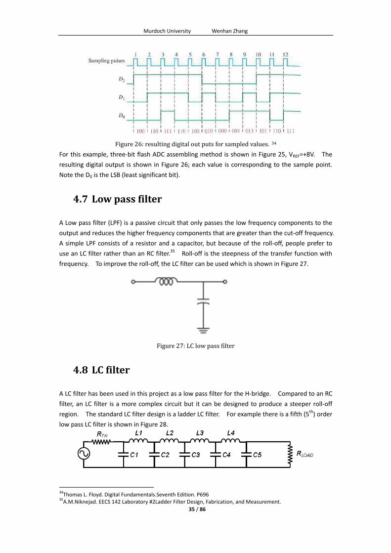
4.7 Low pass filter
A Low pass filter (LPF) is a passive circuit that only passes the low frequency components to the
output and reduces the higher frequency components that are greater than the cut-off frequency.
A simple LPF consists of a resistor and a capacitor, but because of the roll-off, people prefer to
use an LC filter rather than an RC filter.35 Roll-off is the steepness of the transfer function with
frequency. To improve the roll-off, the LC filter can be used which is shown in Figure 27.
Figure 27: LC low pass filter
4.8 LC filter
A LC filter has been used in this project as a low pass filter for the H-bridge. Compared to an RC
filter, an LC filter is a more complex circuit but it can be designed to produce a steeper roll-off
region. The standard LC filter design is a ladder LC filter. For example there is a fifth (5th) order
low pass LC filter is shown in Figure 28.
34
Thomas L. Floyd. Digital Fundamentals.Seventh Edition. P696 35
A.M.Niknejad. EECS 142 Laboratory #2Ladder Filter Design, Fabrication, and Measurement.

Murdoch University Wenhan Zhang
36 / 86
Figure 28: fifth order low pass LC filter36
Some remarks on LC filters:37
The higher order of LC filter will cause a higher cut-off frequency, while this always need a
balanced output phase.
The ideal LC filter does not consume power anymore because it does not have any resistive
element. But the load of an output can cause a significant shift of the f3dB point.
LC filter is a common device for Radio Frequency (RF) circuits which has a bandwidth to
respond the high frequency.
Note: the f3dB is the cutoff frequency for the point 3 dB point below the pass band value. Specified in
normalized frequency units.
36
Eugeniy E. Mikhailov. Physics 252 - Electronics I: Introduction to Analog Circuits.Chapter 4: Passive Analog Signal Processing 37
Eugeniy E. Mikhailov. Physics 252 - Electronics I: Introduction to Analog Circuits.Chapter 4: Passive Analog Signal Processing.
Murdoch University Wenhan Zhang
37 / 86
5 Main board design
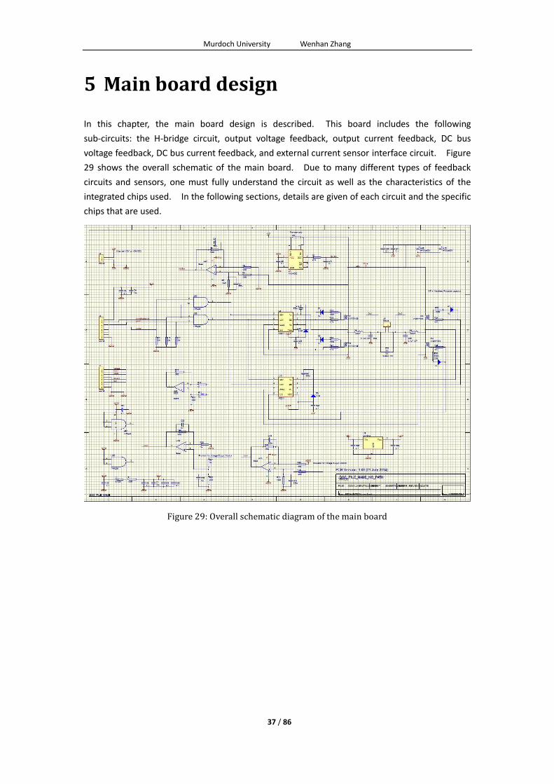
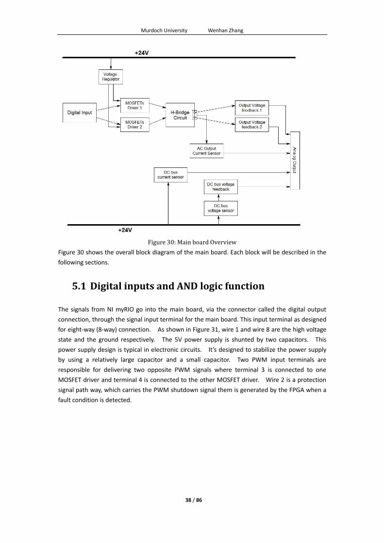
In this chapter, the main board design is described. This board includes the following
sub-circuits: the H-bridge circuit, output voltage feedback, output current feedback, DC bus
voltage feedback, DC bus current feedback, and external current sensor interface circuit. Figure
29 shows the overall schematic of the main board. Due to many different types of feedback
circuits and sensors, one must fully understand the circuit as well as the characteristics of the
integrated chips used. In the following sections, details are given of each circuit and the specific
chips that are used.
Figure 29: Overall schematic diagram of the main board
Murdoch University Wenhan Zhang
38 / 86
Figure 30: Main board Overview
Figure 30 shows the overall block diagram of the main board. Each block will be described in the
following sections.
5.1 Digital inputs and AND logic function
The signals from NI myRIO go into the main board, via the connector called the digital output
connection, through the signal input terminal for the main board. This input terminal as designed
for eight-way (8-way) connection. As shown in Figure 31, wire 1 and wire 8 are the high voltage
state and the ground respectively. The 5V power supply is shunted by two capacitors. This
power supply design is typical in electronic circuits. It’s designed to stabilize the power supply
by using a relatively large capacitor and a small capacitor. Two PWM input terminals are
responsible for delivering two opposite PWM signals where terminal 3 is connected to one
MOSFET driver and terminal 4 is connected to the other MOSFET driver. Wire 2 is a protection
signal path way, which carries the PWM shutdown signal them is generated by the FPGA when a
fault condition is detected.
Murdoch University Wenhan Zhang
39 / 86
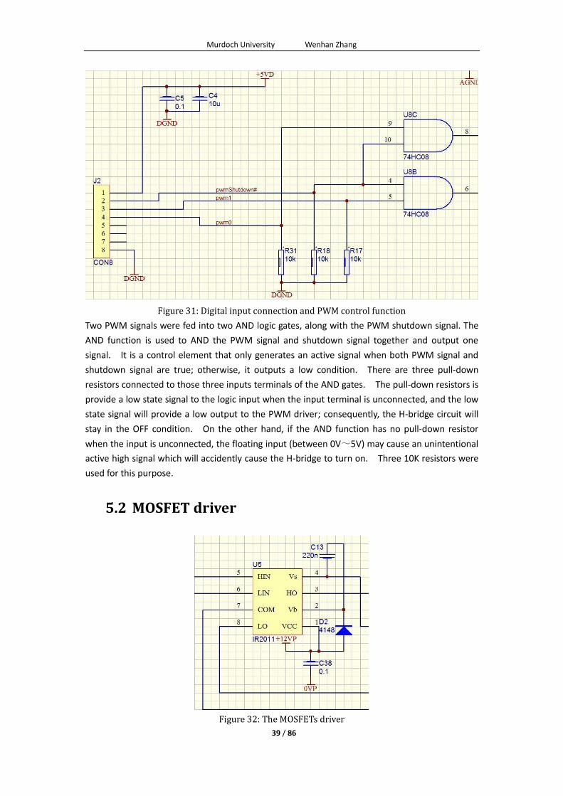
Figure 31: Digital input connection and PWM control function
Two PWM signals were fed into two AND logic gates, along with the PWM shutdown signal. The
AND function is used to AND the PWM signal and shutdown signal together and output one
signal. It is a control element that only generates an active signal when both PWM signal and
shutdown signal are true; otherwise, it outputs a low condition. There are three pull-down
resistors connected to those three inputs terminals of the AND gates. The pull-down resistors is
provide a low state signal to the logic input when the input terminal is unconnected, and the low
state signal will provide a low output to the PWM driver; consequently, the H-bridge circuit will
stay in the OFF condition. On the other hand, if the AND function has no pull-down resistor
when the input is unconnected, the floating input (between 0V~5V) may cause an unintentional
active high signal which will accidently cause the H-bridge to turn on. Three 10K resistors were
used for this purpose.
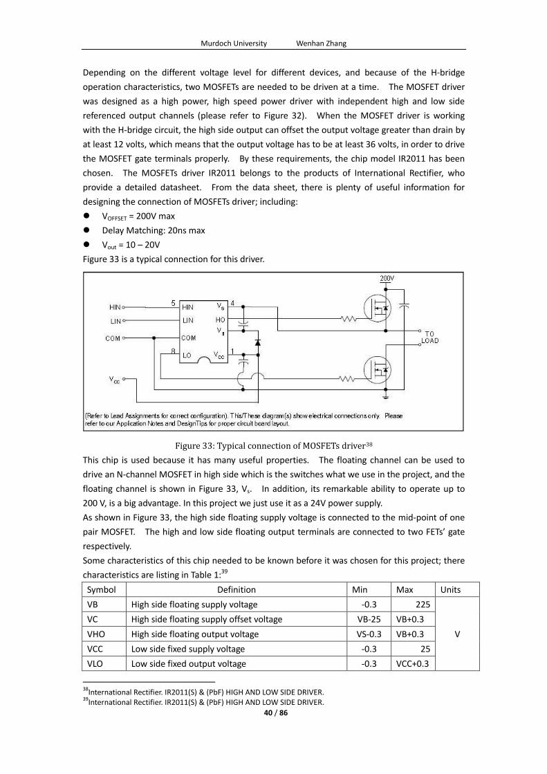
5.2 MOSFET driver
Figure 32: The MOSFETs driver
Murdoch University Wenhan Zhang
40 / 86
Depending on the different voltage level for different devices, and because of the H-bridge
operation characteristics, two MOSFETs are needed to be driven at a time. The MOSFET driver
was designed as a high power, high speed power driver with independent high and low side
referenced output channels (please refer to Figure 32). When the MOSFET driver is working
with the H-bridge circuit, the high side output can offset the output voltage greater than drain by
at least 12 volts, which means that the output voltage has to be at least 36 volts, in order to drive
the MOSFET gate terminals properly. By these requirements, the chip model IR2011 has been
chosen. The MOSFETs driver IR2011 belongs to the products of International Rectifier, who
provide a detailed datasheet. From the data sheet, there is plenty of useful information for
designing the connection of MOSFETs driver; including:
VOFFSET = 200V max
Delay Matching: 20ns max
Vout = 10 – 20V
Figure 33 is a typical connection for this driver.
Figure 33: Typical connection of MOSFETs driver38
This chip is used because it has many useful properties. The floating channel can be used to
drive an N-channel MOSFET in high side which is the switches what we use in the project, and the
floating channel is shown in Figure 33, Vs. In addition, its remarkable ability to operate up to
200 V, is a big advantage. In this project we just use it as a 24V power supply.
As shown in Figure 33, the high side floating supply voltage is connected to the mid-point of one
pair MOSFET. The high and low side floating output terminals are connected to two FETs’ gate
respectively.
Some characteristics of this chip needed to be known before it was chosen for this project; there
characteristics are listing in Table 1:39
Symbol Definition Min Max Units
VB High side floating supply voltage -0.3 225
V
VC High side floating supply offset voltage VB-25 VB+0.3
VHO High side floating output voltage VS-0.3 VB+0.3
VCC Low side fixed supply voltage -0.3 25
VLO Low side fixed output voltage -0.3 VCC+0.3
38
International Rectifier. IR2011(S) & (PbF) HIGH AND LOW SIDE DRIVER. 39
International Rectifier. IR2011(S) & (PbF) HIGH AND LOW SIDE DRIVER.
Murdoch University Wenhan Zhang
41 / 86
VIN Logic input voltage (HIN & LIN) -0.3 VCC+0.3
dVS/dt Allowable offset supply voltage transient - 50 V/ns
TJ Junction temperature - 150
℃ TS Storage temperature -55 150
TL Lead temperature (soldering, 10 seconds) - 300
Table 1: Characteristics of MOSFETs driver
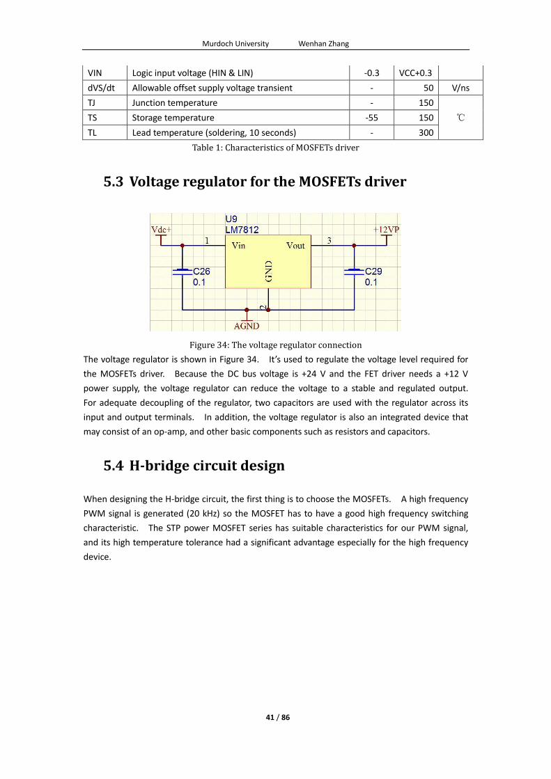
5.3 Voltage regulator for the MOSFETs driver
Figure 34: The voltage regulator connection
The voltage regulator is shown in Figure 34. It’s used to regulate the voltage level required for
the MOSFETs driver. Because the DC bus voltage is +24 V and the FET driver needs a +12 V
power supply, the voltage regulator can reduce the voltage to a stable and regulated output.
For adequate decoupling of the regulator, two capacitors are used with the regulator across its
input and output terminals. In addition, the voltage regulator is also an integrated device that
may consist of an op-amp, and other basic components such as resistors and capacitors.
5.4 H-bridge circuit design
When designing the H-bridge circuit, the first thing is to choose the MOSFETs. A high frequency
PWM signal is generated (20 kHz) so the MOSFET has to have a good high frequency switching
characteristic. The STP power MOSFET series has suitable characteristics for our PWM signal,
and its high temperature tolerance had a significant advantage especially for the high frequency
device.

Murdoch University Wenhan Zhang
42 / 86
Figure 35: H-bridge schematic diagram
Figure 35 is shows the H-bridge circuit. It basically consists of four MOSFETs, one side was
controlled by one MOSFET driver, and the other side was controlled by another driver. When
the H-bridge circuit is working, the power flow from high level to low level can be in two
directions through the load. From Q3 to Q2, or from Q1 to Q4. Two MOSFETs with high voltage
level are directly connected to the +24 V power supply, and two MOSFETs with low level are
connected to the ground. The LC filters are low pass filters; that are used to filter the high
frequency components from the H-bridge output. Therefore, the output voltage has a cleaner
signal with the variable frequency between 50 Hz to 60 Hz, with minimal switching frequency
component.
There is a design for faster turn off option for each MOSFET. It was composed of a diode and a
resistor, and parallel with the original circuit. For faster turn off, the gate terminal can discharge
via the diode path as well. However, this faster turn off feature was not required for this project.
The design was kept in the schematic diagram for future use, if required. At last, a small
capacitor was placed in parallel across the load; this capacitor has the same function as the LC
filter it is used to further attenuate the switching frequency component.
Murdoch University Wenhan Zhang
43 / 86
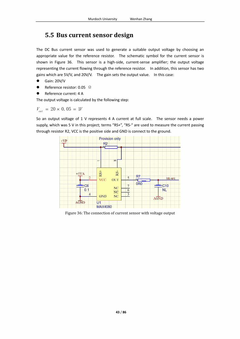
5.5 Bus current sensor design
The DC Bus current sensor was used to generate a suitable output voltage by choosing an
appropriate value for the reference resistor. The schematic symbol for the current sensor is
shown in Figure 36. This sensor is a high-side, current-sense amplifier; the output voltage
representing the current flowing through the reference resistor. In addition, this sensor has two
gains which are 5V/V, and 20V/V. The gain sets the output value. In this case:
Gain: 20V/V
Reference resistor: 0.05 Ω
Reference current: 4 A
The output voltage is calculated by the following step:
20 0.05 1outV V
So an output voltage of 1 V represents 4 A current at full scale. The sensor needs a power
supply, which was 5 V in this project; terms “RS+”, “RS-“ are used to measure the current passing
through resistor R2, VCC is the positive side and GND is connect to the ground.
Figure 36: The connection of current sensor with voltage output
Murdoch University Wenhan Zhang
44 / 86
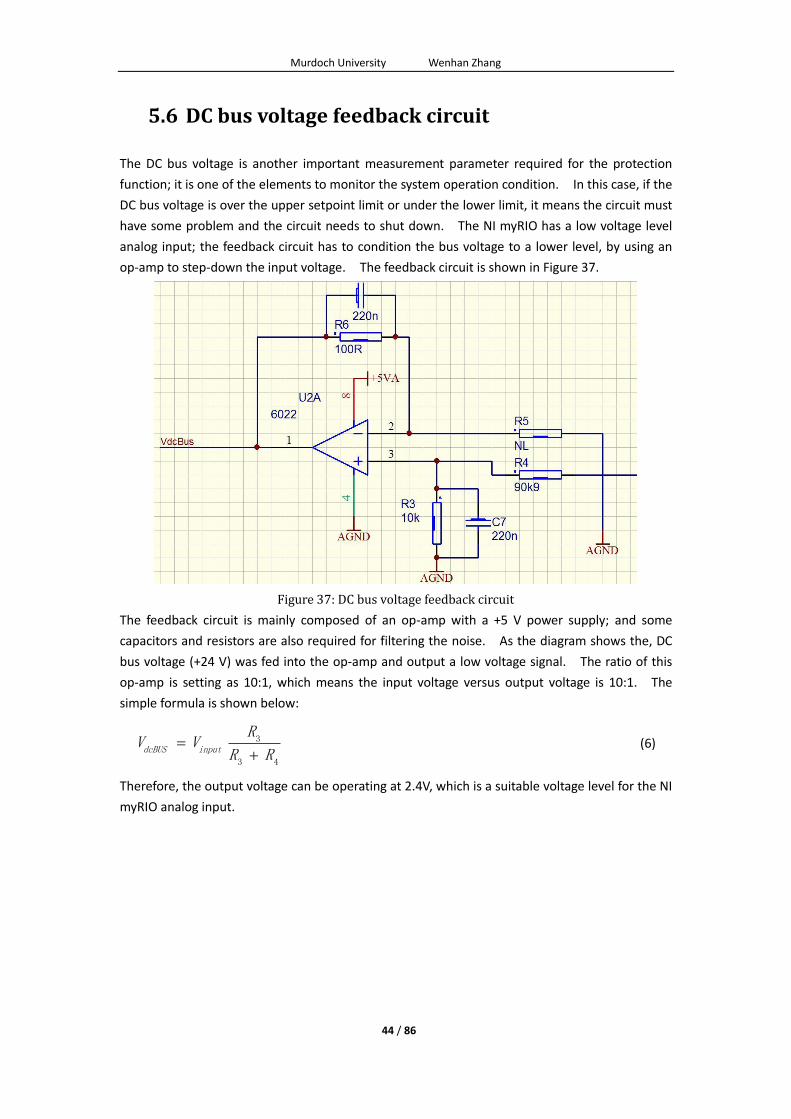
5.6 DC bus voltage feedback circuit
The DC bus voltage is another important measurement parameter required for the protection
function; it is one of the elements to monitor the system operation condition. In this case, if the
DC bus voltage is over the upper setpoint limit or under the lower limit, it means the circuit must
have some problem and the circuit needs to shut down. The NI myRIO has a low voltage level
analog input; the feedback circuit has to condition the bus voltage to a lower level, by using an
op-amp to step-down the input voltage. The feedback circuit is shown in Figure 37.
Figure 37: DC bus voltage feedback circuit
The feedback circuit is mainly composed of an op-amp with a +5 V power supply; and some
capacitors and resistors are also required for filtering the noise. As the diagram shows the, DC
bus voltage (+24 V) was fed into the op-amp and output a low voltage signal. The ratio of this
op-amp is setting as 10:1, which means the input voltage versus output voltage is 10:1. The
simple formula is shown below:
3
3 4
dcBUS input
RV V
R R
(6)
Therefore, the output voltage can be operating at 2.4V, which is a suitable voltage level for the NI
myRIO analog input.
Murdoch University Wenhan Zhang
45 / 86
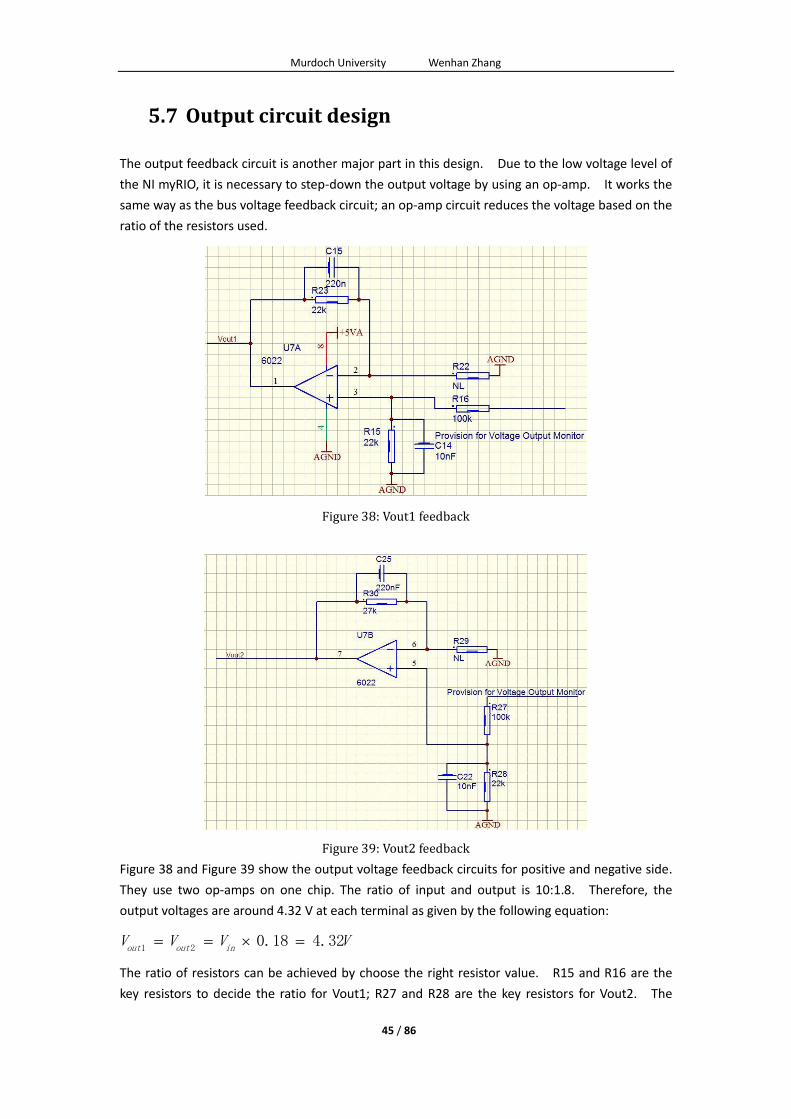
5.7 Output circuit design
The output feedback circuit is another major part in this design. Due to the low voltage level of
the NI myRIO, it is necessary to step-down the output voltage by using an op-amp. It works the
same way as the bus voltage feedback circuit; an op-amp circuit reduces the voltage based on the
ratio of the resistors used.
Figure 38: Vout1 feedback
Figure 39: Vout2 feedback
Figure 38 and Figure 39 show the output voltage feedback circuits for positive and negative side.
They use two op-amps on one chip. The ratio of input and output is 10:1.8. Therefore, the
output voltages are around 4.32 V at each terminal as given by the following equation:
1 20.18 4.32
out out inV V V V
The ratio of resistors can be achieved by choose the right resistor value. R15 and R16 are the
key resistors to decide the ratio for Vout1; R27 and R28 are the key resistors for Vout2. The
Murdoch University Wenhan Zhang
46 / 86
value of those resistors is set to 100k ohms and 22k ohms respectively. In the beginning of its
design, the values were different: R27 and R28 were equal to 0 ohm which is equal short circuit;
R15 and R16 were both equal to 100k ohms. So the op-amp ratio was one (1), which means the
input and output voltage is same. After that, it was found that the output voltage was too high
for the analog signal, and then the new resistance values were chosen.
5.8 Amid generator
The “amid” generator was required as the op-amp circuits were used in a single-supply design
(+5V) (not a dual supply design e.g. +/-5V).
The “amid” generator was a simple voltage reference that is often used in single-supply analog
designs. In this case, the voltage reference provides a fixed low level voltage reference to the
current feedback op-amp. This amid generator was composed of a precision micro-power shunt
voltage reference and some necessary resistors and capacitors. The major part is the voltage
reference, which is an optional value of voltage reference; it can have fixed output voltage of
2.048 V, 2.5 v, 3 V, 4.096 V etc. Depend on the requirements of the current feedback op-amp
and its input range, the output with a 2.048 V voltage reference has been chosen. That device
was connected to the +5 V power supply in series with a resistor; and the output was send to the
amid output terminal. In addition, one test point was created for development use: e.g. for
multimeter or other equipment to check the working condition and output signal. Figure 40
shows the circuits for the amid generator.
Figure 40: The Amid signal generator connection
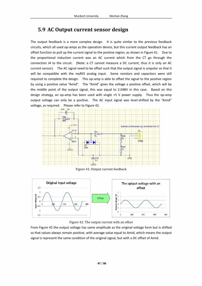
Murdoch University Wenhan Zhang
47 / 86
5.9 AC Output current sensor design
The output feedback is a more complex design. It is quite similar to the previous feedback
circuits, which all used op-amps as the operation device, but this current output feedback has an
offset function to pull up the current signal to the positive region, as shown in Figure 41. Due to
the proportional induction current was an AC current which from the CT go through the
connection J4 to the circuit. (Note: a CT cannot measure a DC current, thus it is only an AC
current sensor). The AC signal need to be offset such that the output signal is unipolar so that it
will be compatible with the myRIO analog input. Some resistors and capacitors were still
required to complete the design. This op-amp is able to offset the signal to the positive region
by using a positive value “Amid”. The “Amid” gives the voltage a positive offset, which will be
the middle point of the output signal, this was equal to 2.048V in this case. Based on this
design strategy, an op-amp has been used with single +5 V power supply. Thus the op-amp
output voltage can only be a positive. The AC input signal was level-shifted by the “Amid”
voltage, as required. Please refer to Figure 42.
Figure 41: Output current feedback
Figure 42: The output current with an offset
From Figure 42 the output voltage has same amplitude as the original voltage form but is shifted
so that values always remain positive, with average value equal to Amid, which means the output
signal is represent the same condition of the original signal, but with a DC offset of Amid.
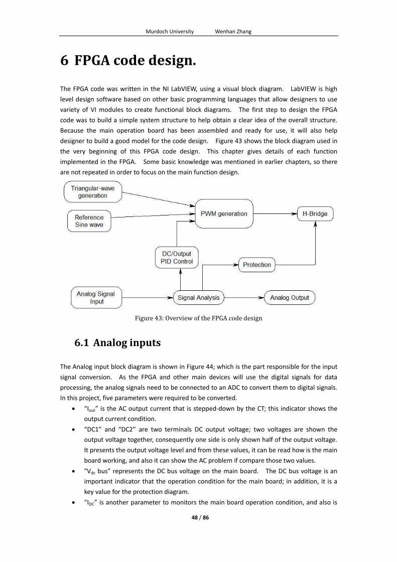
Murdoch University Wenhan Zhang
48 / 86
6 FPGA code design.
The FPGA code was written in the NI LabVIEW, using a visual block diagram. LabVIEW is high
level design software based on other basic programming languages that allow designers to use
variety of VI modules to create functional block diagrams. The first step to design the FPGA
code was to build a simple system structure to help obtain a clear idea of the overall structure.
Because the main operation board has been assembled and ready for use, it will also help
designer to build a good model for the code design. Figure 43 shows the block diagram used in
the very beginning of this FPGA code design. This chapter gives details of each function
implemented in the FPGA. Some basic knowledge was mentioned in earlier chapters, so there
are not repeated in order to focus on the main function design.
Figure 43: Overview of the FPGA code design
6.1 Analog inputs
The Analog input block diagram is shown in Figure 44; which is the part responsible for the input
signal conversion. As the FPGA and other main devices will use the digital signals for data
processing, the analog signals need to be connected to an ADC to convert them to digital signals.
In this project, five parameters were required to be converted.
“Iout” is the AC output current that is stepped-down by the CT; this indicator shows the
output current condition.
“DC1” and “DC2” are two terminals DC output voltage; two voltages are shown the
output voltage together, consequently one side is only shown half of the output voltage.
It presents the output voltage level and from these values, it can be read how is the main
board working, and also it can show the AC problem if compare those two values.
"Vdc bus” represents the DC bus voltage on the main board. The DC bus voltage is an
important indicator that the operation condition for the main board; in addition, it is a
key value for the protection diagram.
“IDC” is another parameter to monitors the main board operation condition, and also is
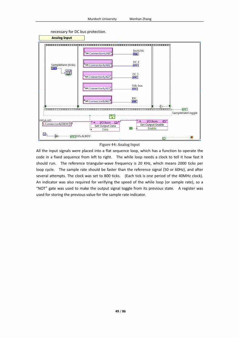
Murdoch University Wenhan Zhang
49 / 86
necessary for DC bus protection.
Figure 44: Analog Input
All the input signals were placed into a flat sequence loop, which has a function to operate the
code in a fixed sequence from left to right. The while loop needs a clock to tell it how fast it
should run. The reference triangular-wave frequency is 20 KHz, which means 2000 ticks per
loop cycle. The sample rate should be faster than the reference signal (50 or 60Hz), and after
several attempts. The clock was set to 800 ticks. (Each tick is one period of the 40MHz clock).
An indicator was also required for verifying the speed of the while loop (or sample rate), so a
“NOT” gate was used to make the output signal toggle from its previous state. A register was
used for storing the previous value for the sample rate indicator.
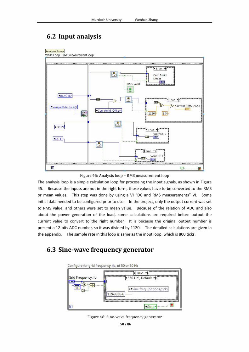
Murdoch University Wenhan Zhang
50 / 86
6.2 Input analysis
Figure 45: Analysis loop – RMS measurement loop
The analysis loop is a simple calculation loop for processing the input signals, as shown in Figure
45. Because the inputs are not in the right form, those values have to be converted to the RMS
or mean values. This step was done by using a VI “DC and RMS measurements” VI. Some
initial data needed to be configured prior to use. In the project, only the output current was set
to RMS value, and others were set to mean value. Because of the relation of ADC and also
about the power generation of the load, some calculations are required before output the
current value to convert to the right number. It is because the original output number is
present a 12-bits ADC number, so it was divided by 1120. The detailed calculations are given in
the appendix. The sample rate in this loop is same as the input loop, which is 800 ticks.
6.3 Sine-wave frequency generator
Figure 46: Sine-wave frequency generator
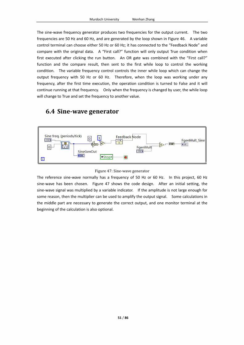
Murdoch University Wenhan Zhang
51 / 86
The sine-wave frequency generator produces two frequencies for the output current. The two
frequencies are 50 Hz and 60 Hz, and are generated by the loop shown in Figure 46. A variable
control terminal can choose either 50 Hz or 60 Hz; it has connected to the “Feedback Node” and
compare with the original data. A “First call?” function will only output True condition when
first executed after clicking the run button. An OR gate was combined with the “First call?”
function and the compare result, then sent to the first while loop to control the working
condition. The variable frequency control controls the inner while loop which can change the
output frequency with 50 Hz or 60 Hz. Therefore, when the loop was working under any
frequency, after the first time execution, the operation condition is turned to False and it will
continue running at that frequency. Only when the frequency is changed by user, the while loop
will change to True and set the frequency to another value.
6.4 Sine-wave generator
Figure 47: Sine-wave generator
The reference sine-wave normally has a frequency of 50 Hz or 60 Hz. In this project, 60 Hz
sine-wave has been chosen. Figure 47 shows the code design. After an initial setting, the
sine-wave signal was multiplied by a variable indicator. If the amplitude is not large enough for
some reason, then the multiplier can be used to amplify the output signal. Some calculations in
the middle part are necessary to generate the correct output, and one monitor terminal at the
beginning of the calculation is also optional.

Murdoch University Wenhan Zhang
52 / 86
6.5 PWM generation loop
Figure 48: The PWM generation loop
Because of many theory of the operation in this project, the PWM generation is one of the most
important parts in the FPGA code design. Figure 48 shows the PWM generation loop which was
built in a single-cycle timing loop (SCTL). The timing loop executes within 1 clock cycle (a fixed
global FPGA 40MHz clock). A select function accounts for different working conditions: when
the PID is working, then the PWM generation will take the “PID control SineOut” as the reference
signal, otherwise, it will use the original one. The triangular-wave signal was generates by a
specialized VI; the frequency was set to 20 KHz. As described in an earlier chapter, the PWM
signal is produced by a comparison function; and two outputs have a dead time control. The
unit of dead time is a tick and it was set to 5 ticks. This value was an experimental value, while
the basic theory is the same, which the value must much smaller than the PWM period.
An “AND” function control was connected to the while loop only when all three conditions are
True will the PWM signal be sent to the load.
The last part in this loop is for the protection of the H-Bridge circuit. Because the H-Bridge
circuit is responsible for the current output, which can deliver high power to the load; it is the
circuit that is most vulnerable to damage. Therefore, the H-Bridge circuit needs adequate
protection to avoid damage. The local variable is a combination signal from the protection loop
and when the fault occurs, it will shut-down the H-bridge circuit. Because the fault signal is
active-high, it needs to convert to active-low through a “NOT” gate, and then combine with the
original output by an “AND” gate.
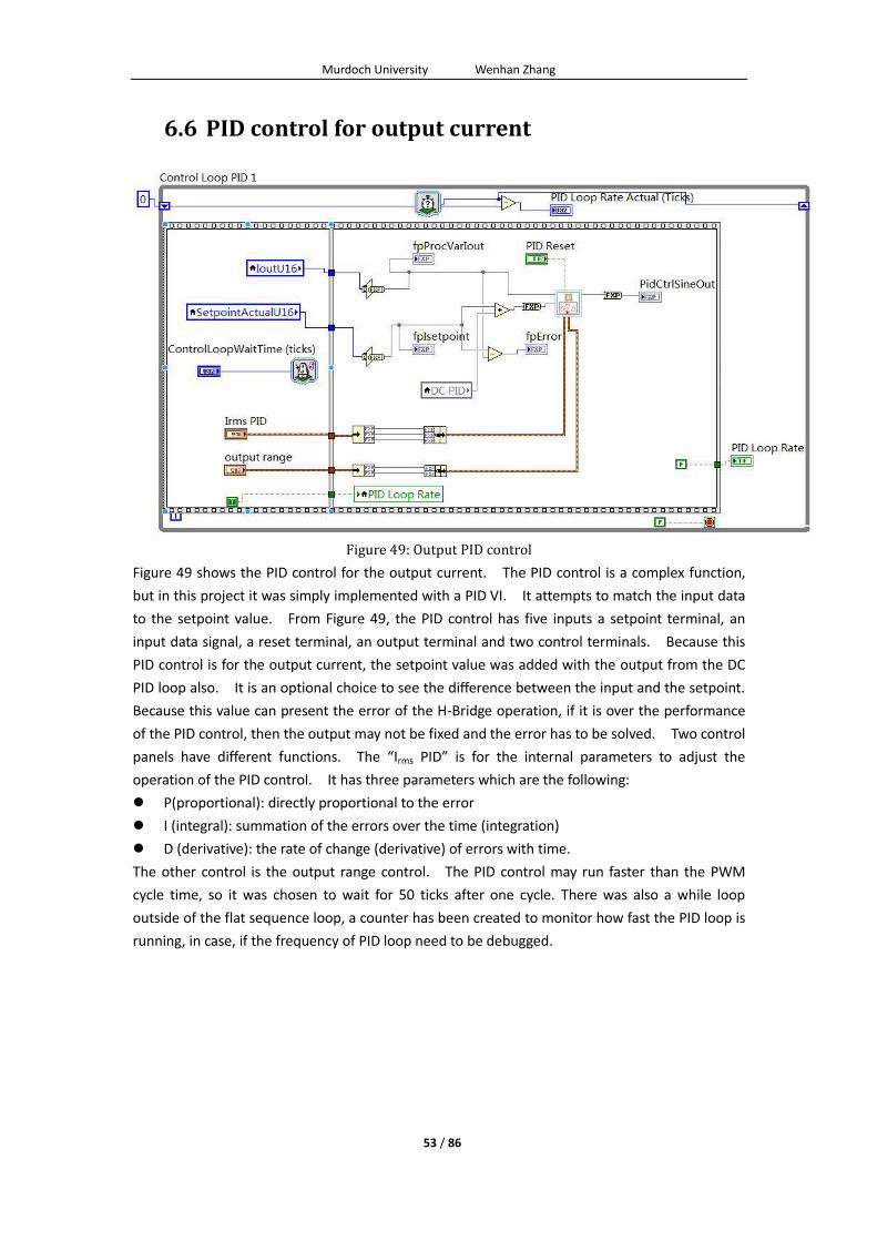
Murdoch University Wenhan Zhang
53 / 86
6.6 PID control for output current
Figure 49: Output PID control
Figure 49 shows the PID control for the output current. The PID control is a complex function,
but in this project it was simply implemented with a PID VI. It attempts to match the input data
to the setpoint value. From Figure 49, the PID control has five inputs a setpoint terminal, an
input data signal, a reset terminal, an output terminal and two control terminals. Because this
PID control is for the output current, the setpoint value was added with the output from the DC
PID loop also. It is an optional choice to see the difference between the input and the setpoint.
Because this value can present the error of the H-Bridge operation, if it is over the performance
of the PID control, then the output may not be fixed and the error has to be solved. Two control
panels have different functions. The “Irms PID” is for the internal parameters to adjust the
operation of the PID control. It has three parameters which are the following:
P(proportional): directly proportional to the error
I (integral): summation of the errors over the time (integration)
D (derivative): the rate of change (derivative) of errors with time.
The other control is the output range control. The PID control may run faster than the PWM
cycle time, so it was chosen to wait for 50 ticks after one cycle. There was also a while loop
outside of the flat sequence loop, a counter has been created to monitor how fast the PID loop is
running, in case, if the frequency of PID loop need to be debugged.
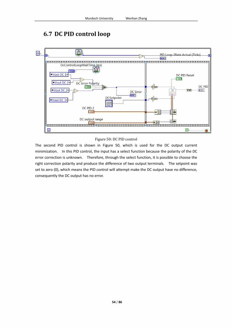
Murdoch University Wenhan Zhang
54 / 86
6.7 DC PID control loop
Figure 50: DC PID control
The second PID control is shown in Figure 50, which is used for the DC output current
minimization. In this PID control, the input has a select function because the polarity of the DC
error correction is unknown. Therefore, through the select function, it is possible to choose the
right correction polarity and produce the difference of two output terminals. The setpoint was
set to zero (0), which means the PID control will attempt make the DC output have no difference,
consequently the DC output has no error.

Murdoch University Wenhan Zhang
55 / 86
6.8 Protection loop design
Figure 51: The protection loop
The protection loop design was a higher level feature. Without this loop, the current source has
already achieved its functional objective. However, for improved reliability, this is a necessary
and important feature for most power electronic applications. In the real condition, it is
possible to get some operation error and the error may cause a serious problem in the circuit,
such as a short-circuit condition. Some of the problems can easily damage some components.
For example, the short-circuit condition may cause a huge current flow through the circuit and
damage the MOSFETs. Some faults are very difficult to fully protect against, but some
protection can extend the hardware survival rate when these conditions occur. Figure 51 shows
the protection loop designed for the current source. It is divided into three parts:
The DC bus voltage protection,
The DC bus current protection, and
The output voltage protection.
The basic method is for the FPGA to compare the inputs against the setpoints. If the input data
is greater than the maximum setpoint or lower than the minimum setpoint, then the false signal
is asserted, and then the system will shut-down. An OR function is used to OR all the
comparison results together, such that even if only one fault condition occurs, the OR gate will
assert a Fault signal to shut-down the system.

Murdoch University Wenhan Zhang
56 / 86
6.9 Output loop design
Figure 52: The analog output design
The analog output port is used for development purposes to monitor the waveforms of the
output signals (please refer to Figure 52). Due to the limited number available for pins of the
analog outputs, the designer can observe only a limited number of signals. In this project, the
output current, DC PID, actual setpoint for the output current, and the output current controlled
by the PID were chosen. The actual setpoint is the main control to adjust the output from the
current source, it has a magnitude variable to change its magnitude and the PID control can
match the new feedback to the setpoint. The output current and PID control output current are
the same, one is the feedback signal measured by CT, one is the real output current.
6.10 FPGA Front Panel
The FPGA front panel is shown in Figure 53. This panel is a designer control panel that divides
into two parts parameter indicators and user controls.
Figure 53: FPGA front panel

Murdoch University Wenhan Zhang
57 / 86
As shown in Figure 53, there are two different types of user controls:
The numeric entry which is for parameters that affect the system behavior.
Boolean control – to enable or disable a function, etc… For example, the disable/enable
control can be used to stop or start a while loop.
The indicators also have two types:
Numeric value display – e.g. show the output RMS current value.
Status indicator – e.g. the fault status.

Murdoch University Wenhan Zhang
58 / 86
7 Testing, Troubleshooting & Debugging
7.1 Testing the Current Source
The last step of the product development is to test the system's performance. This is the most
important step in the industry work because the testing will verify the quality of the finished
goods, and the testing result will confirm whether the project objective was accomplished or not.
After the FPGA code design and assembly of the main board, the next step is to test the current
source. But before the test, one more thing has to be considered, how much power it needs to
generate. It was considered to produce output power of approximately 35 watts into a 4-ohm
load. In the beginning, the resistors were selected as normal axial hole-through resistors, but
after some experiments, it was found that the power was too high for those resistors, and they
overheated the load. Because the resistors were connected to soldered wires, the very high
temperature caused the solder to melt and disconnected the wiring. Another resistor was
founded. It is called an aluminum housed axial wire-wound panel-mount resistor. As shown in
Figure 54, these resistors are connected by wires and were mounted on the heat-sink, so the
heat-sink can dissipate the power. Another advantage is that this kind of resistor is able to
dissipate more power.
Figure 54: The aluminum housed axial wire-wound panel mount resistor
7.2 Open-circuit Test
When the hardware and software were all ready to be tested, the open-circuit condition testing
was the next task. The open-circuit condition means that the H-Bridge was only connected to
the power supply, but not connected to the load. Consequently, the output voltage was not
affected by the load. This step was the initially test to check out the software and main board
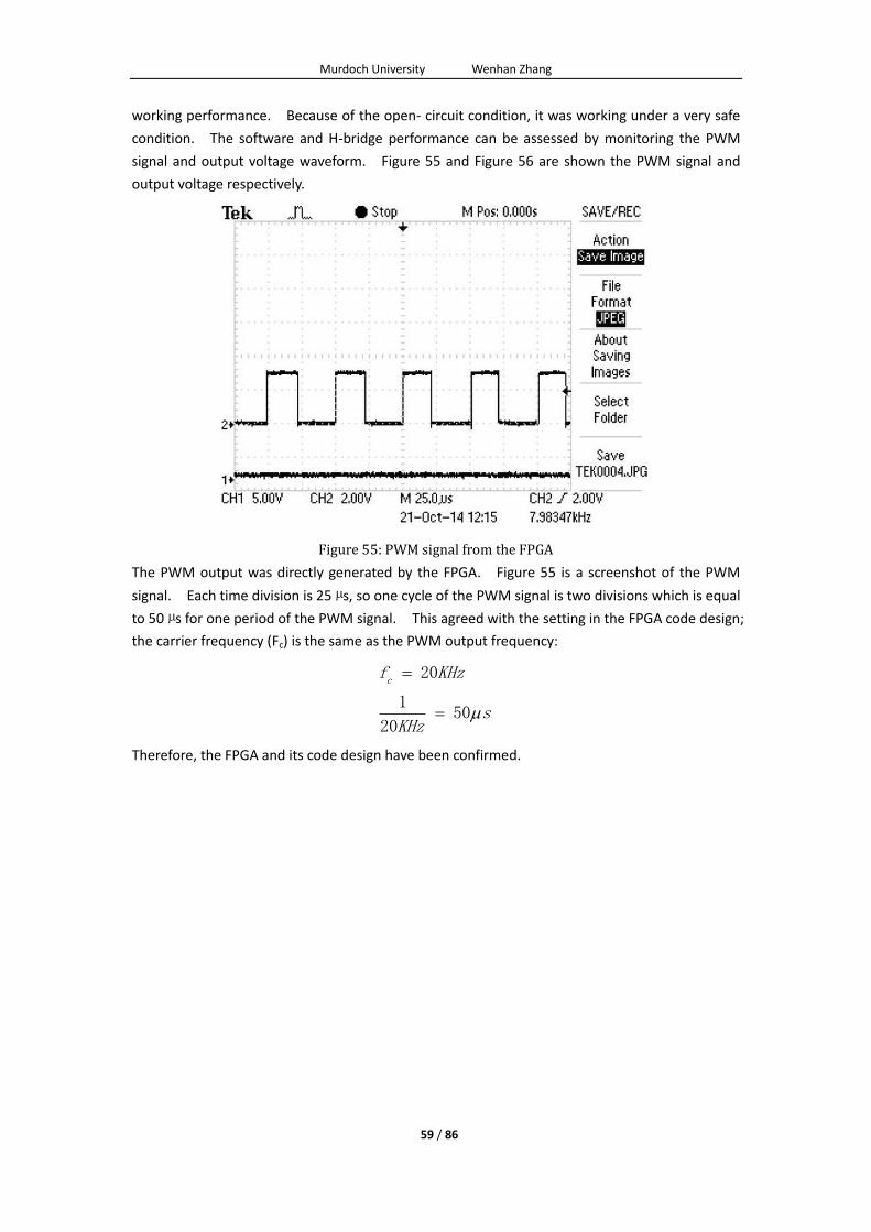
Murdoch University Wenhan Zhang
59 / 86
working performance. Because of the open- circuit condition, it was working under a very safe
condition. The software and H-bridge performance can be assessed by monitoring the PWM
signal and output voltage waveform. Figure 55 and Figure 56 are shown the PWM signal and
output voltage respectively.
Figure 55: PWM signal from the FPGA
The PWM output was directly generated by the FPGA. Figure 55 is a screenshot of the PWM
signal. Each time division is 25 µs, so one cycle of the PWM signal is two divisions which is equal
to 50 µs for one period of the PWM signal. This agreed with the setting in the FPGA code design;
the carrier frequency (Fc) is the same as the PWM output frequency:
20
150
20
cf KHz
sKHz
Therefore, the FPGA and its code design have been confirmed.
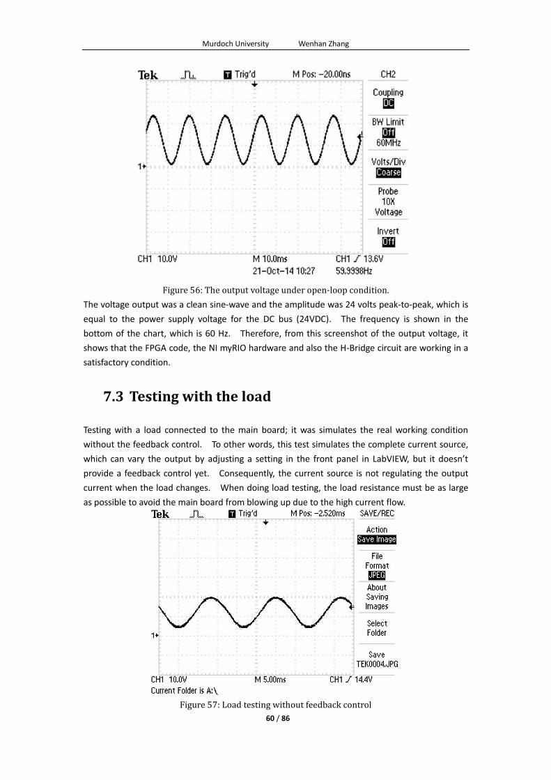
Murdoch University Wenhan Zhang
60 / 86
Figure 56: The output voltage under open-loop condition.
The voltage output was a clean sine-wave and the amplitude was 24 volts peak-to-peak, which is
equal to the power supply voltage for the DC bus (24VDC). The frequency is shown in the
bottom of the chart, which is 60 Hz. Therefore, from this screenshot of the output voltage, it
shows that the FPGA code, the NI myRIO hardware and also the H-Bridge circuit are working in a
satisfactory condition.
7.3 Testing with the load
Testing with a load connected to the main board; it was simulates the real working condition
without the feedback control. To other words, this test simulates the complete current source,
which can vary the output by adjusting a setting in the front panel in LabVIEW, but it doesn’t
provide a feedback control yet. Consequently, the current source is not regulating the output
current when the load changes. When doing load testing, the load resistance must be as large
as possible to avoid the main board from blowing up due to the high current flow.
Figure 57: Load testing without feedback control

Murdoch University Wenhan Zhang
61 / 86
Figure 57 shows the waveform of the output where the load is connected. For safety issue, the
output voltage was set roughly to 10 volts, and the load was the full load which is 4 ohms. The
output voltage can be measured by using a multimeter from the output terminal of the main
board, and it also can be calculated by using the average value in the Figure 57. The current is
also can be measured by use multimeter.
24
1.58
10.18
in
in
out
V V
I A
V V
Then, the output efficiency can be calculated:
2
24 1.58 37.92
10.1825.9
4
68.33%
in
out
out
in
P W
P W
P
P
The efficiency of 70% is generally a bit low for typical electronic devices, but it is acceptable due
to the low load. The output efficiency can be improved by increasing the power supply voltage
and the load. Additional, the quality of main board components may be improved, particularly
for the MOSFETs and filter, by choosing better parts.
On the other hand, the output efficiency can be increased by increasing the amplitude of the
reference sine-wave of the PWM generator, or decreasing the amplitude of triangular-wave both
ways was to increase the duty-cycle of the PWM signal, corresponding to increasing the output
voltage. This way can improve the output efficiency, but unfortunately, it only can improve a bit
3% is the best it can do after some experimentation. However, this method also has some
disadvantages. The major shortcoming of this idea is at increasing the PWM signal will cause a
lot current flow through to the load, and the high current flow may blow up the main board, it
also lead to the input voltage decrease. Therefore, this optimizing method was abandoned.
7.4 Testing With Feedback Control Loop
The previous tests gave reasonable and acceptable. The final testing with the feedback control
was then conducted. The feedback control was implemented in two parts: the feedback circuit
in the main board and the PID control in the FPGA code. By including the feedback control, the
current source can be a complete product in the end. The completed current source was able
to regulate the output current to match the setpoint when the load was varying.
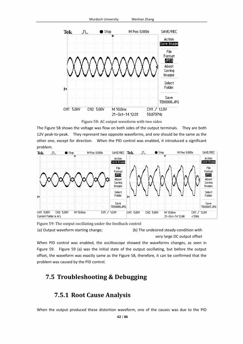
Murdoch University Wenhan Zhang
62 / 86
Figure 58: AC output waveform with two sides
The Figure 58 shows the voltage was flow on both sides of the output terminals. They are both
12V peak-to-peak. They represent two opposite waveforms, and one should be the same as the
other one, except for direction. When the PID control was enabled, it introduced a significant
problem.
Figure 59: The output oscillating under the feedback control
(a) Output waveform starting change; (b) The undesired steady-condition with
very large DC output offset
When PID control was enabled, the oscilloscope showed the waveforms changes, as seen in
Figure 59. Figure 59 (a) was the initial state of the output oscillating, but before the output
offset, the waveform was exactly same as the Figure 58, therefore, it can be confirmed that the
problem was caused by the PID control.
7.5 Troubleshooting & Debugging
7.5.1 Root Cause Analysis
When the output produced these distortion waveform, one of the causes was due to the PID

Murdoch University Wenhan Zhang
63 / 86
controller. The PID controller has three complex variables working together; one has to
understand the working principle of the PID controller, in order to solve this problem.
The three variables are Proportional controller, Integral controller, and Derivative controller.
Proportional controller
The proportional controller is influenced by the present error. The steady state error
inversely proportional to the proportional gain, which means the large proportional gain
lead to a small error. The proportional term is given by:
( )p
P K error t
Integral controller
An integral controller is proportional of the magnitude of the error and also the duration
of the error. The term integral is the summation of the transient errors over the time
and produces an accumulated offset on the output which should be cleared in the past.
The integral control has the ability to eliminate the steady state error, but it may lead to
increased transient errors. The integral term is as follows:
0
( )t
II K error t dt
Derivative controller
The term of derivative can slow the rate of change of the output, thus to optimize the
system stability, decrease the transient error and reduce overshoot. For most of the
low dynamic systems, the derivative is not necessary, but it is important for some of the
more dynamic systems, especially when the other two options are not very helpful.
The derivative term is shown below:
( )D
derror tD K
dt
Form the experience of the previous tests, some features of those three terms can be
summarizing, as given in Table 2.
Parameter Rise Time Overshoot Settling time Steady State error
KP Decrease increase No effects Decrease
KI Decrease increase increase Decrease significantly
KD Slightly Decrease Slightly Decrease Slightly Decrease No effects
Table 2: The features of PID control40
These characteristics must help to control the output current changes to those values could not
solve the DC offset problem. It was thought the problem may be something that the main
board was not able to measure. Therefore, based on the conception of the main board design
and the software design, the problem may be a faulty operation on the board and the current
design has no device to measure it.
After a discussion with the supervisor, it was considered that the problem may cause by the DC
component of the output. A CT was used for current feedback but a CT cannot measure any DC
component. Consequently there is no DC current feedback to monitor the DC output imbalance.
Because of the absence of any DC feedback, even a small DC imbalance will cause a huge
40
PID Control Theory. Kambiz Arab Tehrani and Augustin Mpanda.
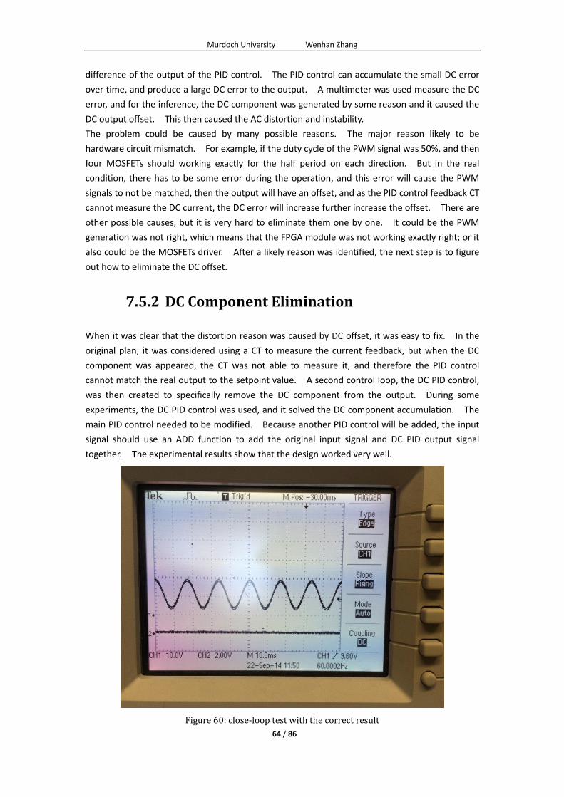
Murdoch University Wenhan Zhang
64 / 86
difference of the output of the PID control. The PID control can accumulate the small DC error
over time, and produce a large DC error to the output. A multimeter was used measure the DC
error, and for the inference, the DC component was generated by some reason and it caused the
DC output offset. This then caused the AC distortion and instability.
The problem could be caused by many possible reasons. The major reason likely to be
hardware circuit mismatch. For example, if the duty cycle of the PWM signal was 50%, and then
four MOSFETs should working exactly for the half period on each direction. But in the real
condition, there has to be some error during the operation, and this error will cause the PWM
signals to not be matched, then the output will have an offset, and as the PID control feedback CT
cannot measure the DC current, the DC error will increase further increase the offset. There are
other possible causes, but it is very hard to eliminate them one by one. It could be the PWM
generation was not right, which means that the FPGA module was not working exactly right; or it
also could be the MOSFETs driver. After a likely reason was identified, the next step is to figure
out how to eliminate the DC offset.
7.5.2 DC Component Elimination
When it was clear that the distortion reason was caused by DC offset, it was easy to fix. In the
original plan, it was considered using a CT to measure the current feedback, but when the DC
component was appeared, the CT was not able to measure it, and therefore the PID control
cannot match the real output to the setpoint value. A second control loop, the DC PID control,
was then created to specifically remove the DC component from the output. During some
experiments, the DC PID control was used, and it solved the DC component accumulation. The
main PID control needed to be modified. Because another PID control will be added, the input
signal should use an ADD function to add the original input signal and DC PID output signal
together. The experimental results show that the design worked very well.
Figure 60: close-loop test with the correct result
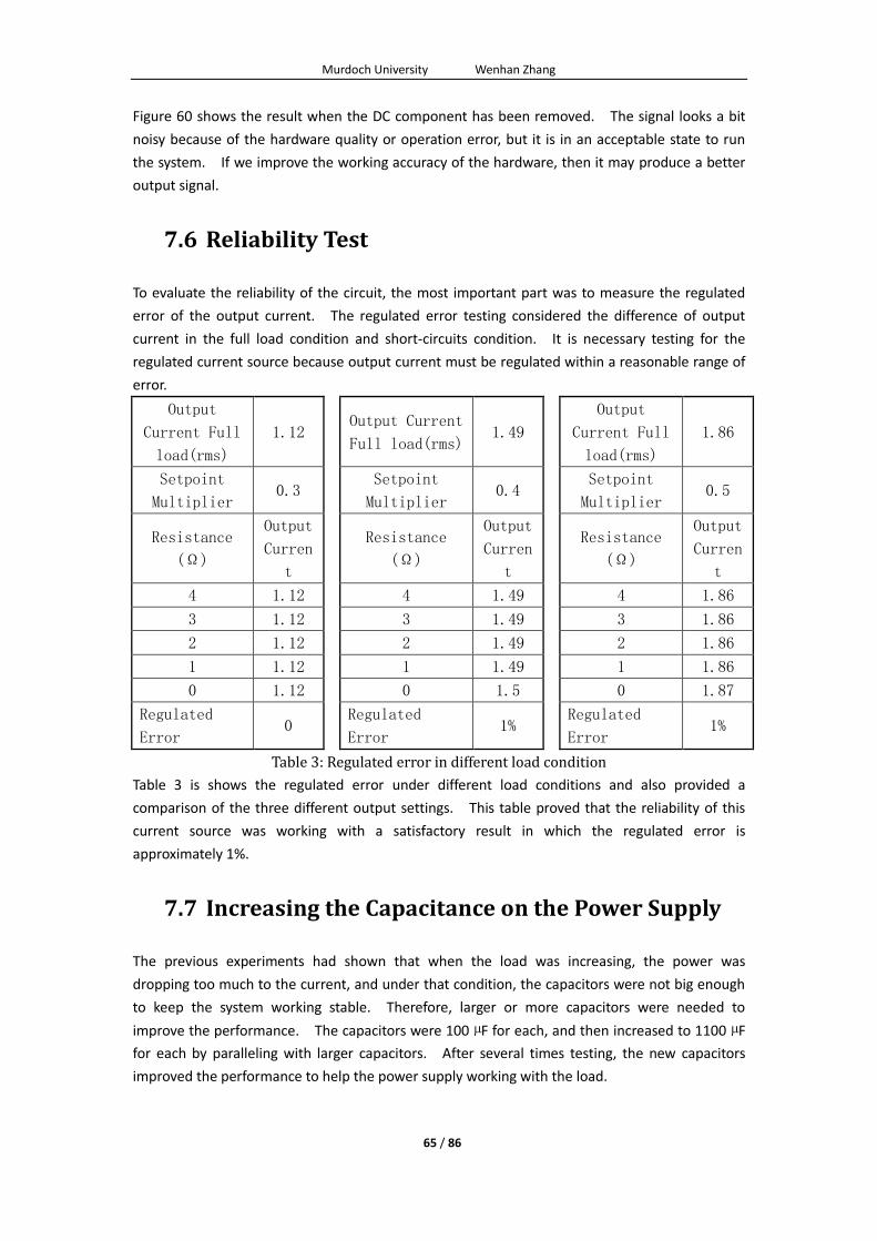
Murdoch University Wenhan Zhang
65 / 86
Figure 60 shows the result when the DC component has been removed. The signal looks a bit
noisy because of the hardware quality or operation error, but it is in an acceptable state to run
the system. If we improve the working accuracy of the hardware, then it may produce a better
output signal.
7.6 Reliability Test
To evaluate the reliability of the circuit, the most important part was to measure the regulated
error of the output current. The regulated error testing considered the difference of output
current in the full load condition and short-circuits condition. It is necessary testing for the
regulated current source because output current must be regulated within a reasonable range of
error.
Output
Current Full
load(rms)
1.12
Output Current
Full load(rms) 1.49
Output
Current Full
load(rms)
1.86
Setpoint
Multiplier 0.3
Setpoint
Multiplier 0.4
Setpoint
Multiplier 0.5
Resistance
(Ω)
Output
Curren
t
Resistance
(Ω)
Output
Curren
t
Resistance
(Ω)
Output
Curren
t
4 1.12
4 1.49
4 1.86
3 1.12
3 1.49
3 1.86
2 1.12
2 1.49
2 1.86
1 1.12
1 1.49
1 1.86
0 1.12
0 1.5
0 1.87
Regulated
Error 0
Regulated
Error 1%
Regulated
Error 1%
Table 3: Regulated error in different load condition
Table 3 is shows the regulated error under different load conditions and also provided a
comparison of the three different output settings. This table proved that the reliability of this
current source was working with a satisfactory result in which the regulated error is
approximately 1%.
7.7 Increasing the Capacitance on the Power Supply
The previous experiments had shown that when the load was increasing, the power was
dropping too much to the current, and under that condition, the capacitors were not big enough
to keep the system working stable. Therefore, larger or more capacitors were needed to
improve the performance. The capacitors were 100 µF for each, and then increased to 1100 µF
for each by paralleling with larger capacitors. After several times testing, the new capacitors
improved the performance to help the power supply working with the load.
Murdoch University Wenhan Zhang
66 / 86
7.8 Protection Design
Due to the past testing, many MOSFETs were damaged because of the DC offset and other
problems. It was decided that protection circuit is necessary for the system, and this would also
be helpful for future testing. Because the main board already has the key characteristics
feedback loop, the protection function was added to the FPGA code. The protection was
divided into three sections: the DC bus voltage protection, the DC bus current protection, and the
output voltage protection.
7.8.1 DC Bus Voltage Protection
The DC bus voltage protection was considered to limit the power supply voltage to a suitable
range. If the product used a battery for its power supply, then the battery voltage may vary, and
it may drop too much voltage or be charged too high, therefore a bus voltage protection is
needed.
The limits of the maximum and minimum setpoints were choosing to be limited +/- 4 volts from
the nominal 24V supply. The values for the setpoints in LabVIEW are all the ADC numbers, the
conversion calculations are shown in the appendix.
7.8.2 DC Bus Over-current Protection
The current protection was only created for the over-current condition. It was considered that
under short-circuit fault conditions, if the system has short-circuited problem, then too much
current will flow, and the over-current protection will shut-down the system. The bus current
protection is independent to the bus voltage protection. As mentioned before, if the power
supply was a battery, the voltage will always maintain the same no matter how the current
change, so these two protections are actually protecting the system from two different
conditions.
The bus current limit was only considered for the maximum limit, which was 4 amperes in this
project. The calculations are shown in the appendix.
7.8.3 Output Voltage Protection
The output voltage control cater for both over-voltage and under-voltage protection. This type
of fault can be caused by load open-circuit condition or by output terminal short-circuit to
ground condition.
The design of protection was simple to implement within LabVIEW. Three parts of the input
signals are selected from the analog inputs and the LabVIEW was used to compare the input
signals against the setpoints. If the applicable input is greater than the maximum setpoint or
lower than the minimum setpoint, the system will be shut down to prevent hardware damage.

Murdoch University Wenhan Zhang
67 / 86
The limit of output voltage protection is different to the previous two protection conditions.
The output range was from 0 to 24 volts and the mid-point was 12 volts. So the limit was
chosen 2 volts higher than the bottom of the range and 2 volts lower than the top of the range.
The calculation is shown in the appendix.
8 Internship evaluation
The internship at Red Phase provided a great working experience in a professional engineering
working environment. This chance gave valuable experience on product design, making and
testing, and in addition it provided a good team work experience. During the internship, it
proves that working effectively, thinking positively, and communicating freely are very important
for a member of an engineering development team. There in a lot of skill and knowledge that
can be learned from others for a new person, and this learning curve is the most precious
experience for a graduate-level engineer. To sum up, the engineering internship has been
completed and most targets have been achieved, except for optimizing a system, which can be
part of the future plan.
8.1 Achievements
The aim of the internship was to create a regulated current source, with variable frequency.
This product will be used for company development work and also will be used as a commercial
product. The achievements are given below:
A stable current source with a maximum of 4A rms output current
The frequency of output current can be chosen as 50Hz or 60Hz
The output power has a maximum value of 50W
The current source has the following protection functions:
1) Open loop protection
2) Over voltage protection
3) Over current protection
The project used some new design tools, and some basic knowledge had to be learnt understood.
As the end of the internship, the following skills and knowledge had been mastered:
LabVIEW programming skill
Solder skill/ PCB assemble skill
Protel 99SE simulating skill
Basic circuit operation theory
H-bridge
LC filter
Operational amplifier
Voltage regulator
Current sensor
MOSFETs driver
Digital fundamentals

Murdoch University Wenhan Zhang
68 / 86
logic gates
Analog to Digital Convertor
Digital to Analog Convertor
Number System (binary numbers, decimal numbers)
PWM theory and its generation
FPGA theory
PID control theory
8.2 Enhanced Areas
As previously mentioned, the main targets of the internship were all achieved. However for all
engineering design, there is always room for improvement, and this project is no different. In
the very beginning of the project plan, the Real-time module was proposed. It providing a useful
control panel those users can acquire information such as the output waveforms, setpoint
waveforms and even the FPGA triangular waveform. Consequently, the Real-time module is
able to provide for waveform monitoring, so it can be used instead of an oscilloscope in the
testing work. Some other enhancements are given below:
8.2.1 Real-time module
This method not only has advantages like operation monitoring, it also represents a higher level
control compare to the FPGA front panel.
Reasonable user interface
This high level control panel would be useful to end users, because the FPGA front panel is
linked to the FPGA block diagram, it cannot be shown to users, because the FPGA code
should be locked from the customer. However it must be made available using some user
interface.
Efficient reprogrammable function
Once the FPGA code has been locked, the user only can manage the Real-time module and it
makes the compiling much shorter than the FPGA compile. This is a significant advantage
for the user that they can save a lot of time in the compiling.
8.2.2 Remote control module
The remote another part that can be optimized. Due to technology development, NI LabVIEW
provides an option to allow for a remote control. The remote control is a human and for
engineering development, because it will enable technical support and field experts to maintain
the products from far away. It only needs an internet connection for both of the customer and
the maintenance crews, and it is convenient for both sides.

Murdoch University Wenhan Zhang
69 / 86
9 References:
1. Red Phase Instruments. (2013, Dec) Product Catalogue 2013-14. [Online]. Available:
http://www.redphase.com.au/Files/Catalogue%202013_Q4.pdf
2. B. Klaus and P. Horn, Robot Vision. Cambridge, MA: MIT Press, 1986.
3. L. Stein, “Random patterns,” in Computers and You, J. S. Brake, Ed. New York: Wiley, 1994, pp.
55-70.
4. Linden T. Harrison. “An introduction to current sources”, in Current sources & voltage
references. 2005, Chapter 2.
5. Richard R. Spencer, “Operational Amplifiers”, in Mohammed S. Ghausi. Introduction Electronic
Circuit Design. 2001, Chapter 5. 6. Thomas L. Floyd. Digital Fundamentals. Prentice Hall, 1999. Seventh Edition.
7. J. Jones. (1991, May 10). Networks (2nd ed.) [Online]. Available: http://www.atm.com
8. Sakshat Virtual Labs. (2014). PCB design & fabrication. [Online]. Available:
http://coep.vlab.co.in/?sub=34&brch=106&sim=241&cnt=1
9. National Instruments. (2014). LabVIEW Environment Basics. [Online]. Available:
http://www.ni.com/getting-started/labview-basics/environment 10/07/2014
10. Ahsan Munir, Syed Hashsham. ENE 806 Laboratory Feasibility Studies fir Environmental
Remediation Introduction to LabVIEW. [Online]. Available FTP: http://www.egr.msu.edu/~hashsham/courses/ Directory: ene806/docs/ File: LabView%20Introduction.pdf
11. ELECTRIC POWER RESEARCH INSTITUTE. DC Power Production, Delivery and Utilization- An
EPRI White Paper. Palo Alto: EPRI. June 2006. 12. Tektronix. Digital Storage Oscilloscopes TDS1000B Series Data Sheet. Beaverton: Tektronix.
25 Sep 2013.
13. National Instruments. USER GUIDE AND SPECIFICATIONS NI myRIO-1900. Austin: National
Instruments. 2013.
14. National Instruments. NI LabVIEW Environment: Detailed Explanation
15. National Instruments. LabVIEW Environment Basics.
16. Scott Hauck, AbdreDehon. Reconfigurable Computing - The Theory and Practice of
FPGA-Based Computation. MA: Morgan Kaufmann, 2008.
17. TeshomeAbabu. Design of Pules Width Modulation (PWM) and it’s Implementation in XILINX
Field Programmable Gate Array (FPGA).
18. Ralph Kennel. Power Electronics Exercise: Pulse Width Modulation Methods 2013. Technische
University Munchen.
19. James Bryant, Walt Jung, Walt Kester. “Op AMP BASICS” in Op AMP Applications Handbook.
Newnes, 2002.
20. James K. Roberge, Kent H. Lundberg. Operational Amplifiers:Theory and Practice. Second
Edition, Version 1.8.1
21. A.M.Niknejad. EECS 142 Laboratory #2Ladder Filter Design, Fabrication, and Measurement.
Berkeley Wireless Research Center, 2008.
22. Eugeniy E. Mikhailov. “Chapter 4: Passive Analog Signal Processing” in Physics 252 -
Electronics I: Introduction to Analog Circuits. [Online]. Available:
http://physics.wm.edu/~evmik/classes/Physics_252_Analog_Electronics/
23. International Rectifier. IR2011(S) & (PbF) HIGH AND LOW SIDE DRIVER. [Online]. Available:
http://www.irf.com/product-info/datasheets/data/ir2011.pdf

Murdoch University Wenhan Zhang
70 / 86
24. Japan UNIX. Laser Soldering: Pinpoint heating is perfect for ultrafine parts or high density
mounting. [Online]. Available:
http://www.fancort.com/PDFs/UNIX_White_Paper_Soldering_Fundamentals_Vol_2_09_D.p
df
25. Surface Mount Design and Land Pattern Standard, IPC-SM-782A, Oct 1996.
26. Acceptability of Printed Boards, IPC-A-600F, Nov 1999.
27. Design Guidelines for Reliable Surface Mount Technology Printed Board Assemblies, IPC-D-279,
Jul 1996.
Murdoch University Wenhan Zhang
71 / 86
Glossary & Explanation
Murdoch University Wenhan Zhang
72 / 86
Murdoch University Wenhan Zhang
73 / 86
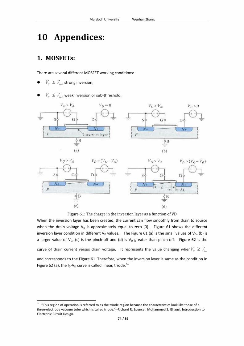
Murdoch University Wenhan Zhang
74 / 86
10 Appendices:
1. MOSFETs:
There are several different MOSFET working conditions:
G thV V , strong inversion;
G thV V , weak inversion or sub-threshold.
Figure 61: The charge in the inversion layer as a function of VD
When the inversion layer has been created, the current can flow smoothly from drain to source
when the drain voltage VD is approximately equal to zero (0). Figure 61 shows the different
inversion layer condition in different VD values. The Figure 61 (a) is the small values of VD, (b) is
a larger value of VD, (c) is the pinch-off and (d) is VD greater than pinch-off. Figure 62 is the
curve of drain current versus drain voltage. It represents the value changing whenG thV V
and corresponds to the Figure 61. Therefore, when the inversion layer is same as the condition in
Figure 62 (a), the ID-VD curve is called linear, triode.41
41
“This region of operation is referred to as the triode region because the characteristics look like those of a three-electrode vacuum tube which is called triode.”--Richard R. Spencer, Mohammed S. Ghausi. Introduction to Electronic Circuit Design.
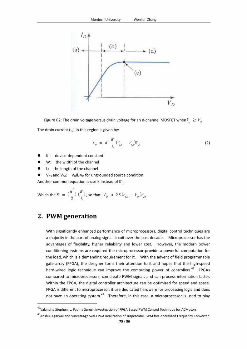
Murdoch University Wenhan Zhang
75 / 86
Figure 62: The drain voltage versus drain voltage for an n-channel MOSFET whenG thV V
The drain current (ID) in this region is given by:
' ( )D GS th DS
WI K V V V
L (2)
K’: device-dependent constant
W: the width of the channel
L: the length of the channel
VGS and VDS: VG& VD for ungrounded source condition
Another common equation is use K instead of K’:
Which the'
( )( )2
K WK
L , so that 2 ( )
D GS th DSI K V V V
2. PWM generation
With significantly enhanced performance of microprocessors, digital control techniques are
a majority in the part of analog signal circuit over the past decade. Microprocessor has the
advantages of flexibility, higher reliability and lower cost. However, the modern power
conditioning systems are required the microprocessor provide a powerful computation for
the load, which is a demanding requirement for it. With the advent of field programmable
gate array (FPGA), the designer turns their attention to it and hopes that the high-speed
hard-wired logic technique can improve the computing power of controllers.42 FPGAs
compared to microprocessors, can create PWM signals and can process information faster.
Within the FPGA, the digital controller architecture can be optimized for speed and space.
FPGA is different to microprocessor, it use dedicated hardware for processing logic and does
not have an operating system.43 Therefore, in this case, a microprocessor is used to play
42
Valantina Stephen, L. Padma Suresh.Investigation of FPGA Based PWM Control Technique for ACMotors. 43
Anshul Agarwal and VineetaAgarwal.FPGA Realization of Trapezoidal PWM forGeneralized Frequency Converter.
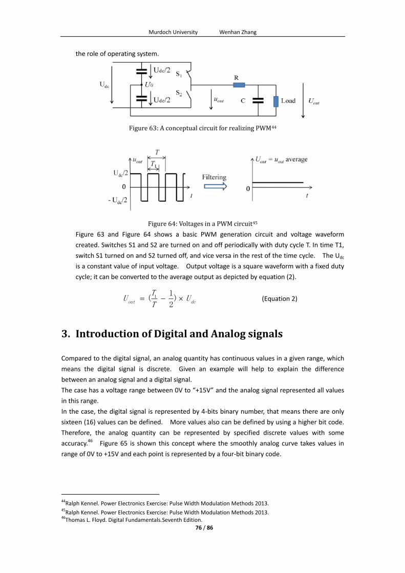
Murdoch University Wenhan Zhang
76 / 86
the role of operating system.
Figure 63: A conceptual circuit for realizing PWM44
Figure 64: Voltages in a PWM circuit45
Figure 63 and Figure 64 shows a basic PWM generation circuit and voltage waveform
created. Switches S1 and S2 are turned on and off periodically with duty cycle T. In time T1,
switch S1 turned on and S2 turned off, and vice versa in the rest of the time cycle. The Udc
is a constant value of input voltage. Output voltage is a square waveform with a fixed duty
cycle; it can be converted to the average output as depicted by equation (2).
1 1( )
2out dc
TU U
T (Equation 2)
3. Introduction of Digital and Analog signals
Compared to the digital signal, an analog quantity has continuous values in a given range, which
means the digital signal is discrete. Given an example will help to explain the difference
between an analog signal and a digital signal.
The case has a voltage range between 0V to “+15V” and the analog signal represented all values
in this range.
In the case, the digital signal is represented by 4-bits binary number, that means there are only
sixteen (16) values can be defined. More values also can be defined by using a higher bit code.
Therefore, the analog quantity can be represented by specified discrete values with some
accuracy.46 Figure 65 is shown this concept where the smoothly analog curve takes values in
range of 0V to +15V and each point is represented by a four-bit binary code.
44
Ralph Kennel. Power Electronics Exercise: Pulse Width Modulation Methods 2013. 45
Ralph Kennel. Power Electronics Exercise: Pulse Width Modulation Methods 2013. 46
Thomas L. Floyd. Digital Fundamentals.Seventh Edition.
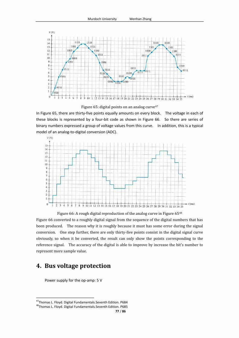
Murdoch University Wenhan Zhang
77 / 86
Figure 65: digital points on an analog curve47
In Figure 65, there are thirty-five points equally amounts on every block. The voltage in each of
these blocks is represented by a four-bit code as shown in Figure 66. So there are series of
binary numbers expressed a group of voltage values from this curve. In addition, this is a typical
model of an analog-to-digital conversion (ADC).
Figure 66: A rough digital reproduction of the analog curve in Figure 6548
Figure 66 converted to a roughly digital signal from the sequence of the digital numbers that has
been produced. The reason why it is roughly because it must has some error during the signal
conversion. One step further, there are only thirty-five points consist in the digital signal curve
obviously, so when it be converted, the result can only show the points corresponding to the
reference signal. The accuracy of the digital is able to improve by increase the bit’s number to
represent more sample value.
4. Bus voltage protection
Power supply for the op-amp: 5 V
47
Thomas L. Floyd. Digital Fundamentals.Seventh Edition. P684 48
Thomas L. Floyd. Digital Fundamentals.Seventh Edition. P685

Murdoch University Wenhan Zhang
78 / 86
,max
,min
24
28
20
bus
bus
bus
V V
V V
V V
After the operation by op-amp (ratio is 10):
,max
,min
2.4
2.8
2.0
bus
bus
bus
V V
V V
V V
Translate to the ADC number:
12
12
2.8,max( ) 2 2294
5
2.0,min( ) 2 1638
5
Vbus ADC
Vbus ADC
a) Bus over-current protection
The current sensor was used 1 volt to present 4 amperes current flow on the bus. Therefore,
the 4 amperes current is the limit of the bus current protection and it can be calculated:
1212 819
5
V
V
b) Output voltage protection
Because of the ratio in the op-amp was around 1:6, and the resistors were chosen 22 kΩ and
100 kΩ. So the limit of output voltage can be calculated by the following steps:
22,max 22 3.96
122
22,min 2 0.36
122
Vout V V
Vout V V
And the ADC numbers are calculated:
12
12
3.96,max( ) 2 3244
5
0.36,min( ) 2 295
5
VVout ADC
V
VVout ADC
V

Murdoch University Wenhan Zhang
79 / 86
c) Regulated error
Table 4: Regulated error measurement
5. Soldering tools
a) Soldering station
In this project, a soldering station (Figure 67) is combination of three soldering iron, which
include one normal soldering iron, a parallel remover, and wave tip soldering iron.
Figure 67: soldering station

Murdoch University Wenhan Zhang
80 / 86
The parallel remover (Figure 68) is specific for people remove electronic components on the PCB,
such as chip capacitors, resistors and inductors. When people want to remove any component,
two parts of the hot iron will touch both side of component and heat the solder to remove it.
Figure 68: Parallel Remover
Figure 69: Wave tip Solder iron
The wave tip soldering iron (Figure 69) is used to solder surface-mount components by hand
(manually). It has a hollow tip, which helps to create extra solder surface tension, which is
useful for soldering fine-pitch devices. It can also be used to remove excess solder, to tidy up
existing solder joints.

Murdoch University Wenhan Zhang
81 / 86
b) Desoldering tool
Figure 70: Desoldering tool
This is a very strong solder vacuum tool for people want to remove all the solder (Figure 70). Its
working principle is like a pump, when compress the spring, it makes the inner space to be
vacuum and when press the button, it will produce a very strong suction to suck up all the solder.
Therefore people can re-solder the component in the same place.
6. Hands-on Assembling Skills
After the main board was designed and fabricated, the next step was to assemble the PCB. This
step was more about hands-on work and the major part was to use the solder-station tools to
solder the components onto the PCB. It was a more interesting part in this project because this
step manufactures the actual physical objects from previous study and design work. But it was
also a part of work that needs to pay more attention to the safety issues. In contrast to past
soldering experience, the author found the soldering task requires finer control to solder the very
small and fine-pitch parts. Thus it required a lot of learning and practice to get it right. Many
industry soldering procedures adhere to various standards such as the IPC standard.
a) Soldering
Soldering is common procedure in electronic assembling processes. There are basically three
steps in the soldering process:
1) Preheat: heating both base and pin to set to the appropriate temperature.
2) Heat: provide the solder around the hole to feed in it. The solder must join the hole nicely
to make a good connection between the base and the pin. It needs to have a shiny finish
with adequate flux coverage to minimize contamination.
3) Post-heat: post heat is the last step to set the shape of the finished solder joint. This step
makes the solder shape to be the typical appearance of a fillet. The “fillet” shape is the
standard appearance for soldering anything; it has a very stable strong structure to hold the
connection.
Figure 71 shows the typical soldering heating process in the industrial manufacture.

Murdoch University Wenhan Zhang
82 / 86
Figure 71: soldering heating process49
b) Soldering & Assemble Standards
Every manufacturer has to comply with the professional industry standards. For the electronics
producer, there are some soldering and assembling standards that also need to be followed.
The Association of Connecting Electronics Industries is the authority for electronics producers,
and their many standards are widely used in this field. Some of main standards were used in
this project are shown below:
IPC-SM-782A Surface Mount Design and Land Pattern Standard: The information about land
pattern used for the surface attachments of electronic components.
IPC-A-600F Acceptability of Printed Boards: describes the acceptable and intolerable visual
on the face of printed board in both of internal and external condition.
IPC-D-279 Design Guidelines for Reliable Surface Mount Technology Printed Board
Assemblies: This document explains the detail of ‘Design for Reliability’ procedures and the
reliability of assemble the PCB.
Based on these documents, producers are able to make products that comply with the standards.
These standards apply to finished goods for the product end users. For experimentation and
development purposes, when engineers and technicians are testing work under development,
the soldering work don’t generally need to meets those standards.
For example, when designer want to test the H-bridge circuit, some extra wires or pins may
needed to be connected to some components, but once the final product is released, the extra
experimental connections, etc..., have to be removed. The final product manufacturing
procedure need to adhere to those standards to ensure acceptable yield and high reliability.
49
Japan UNIX. Laser Soldering: Pinpoint heating is perfect for ultrafine parts or high density mounting.
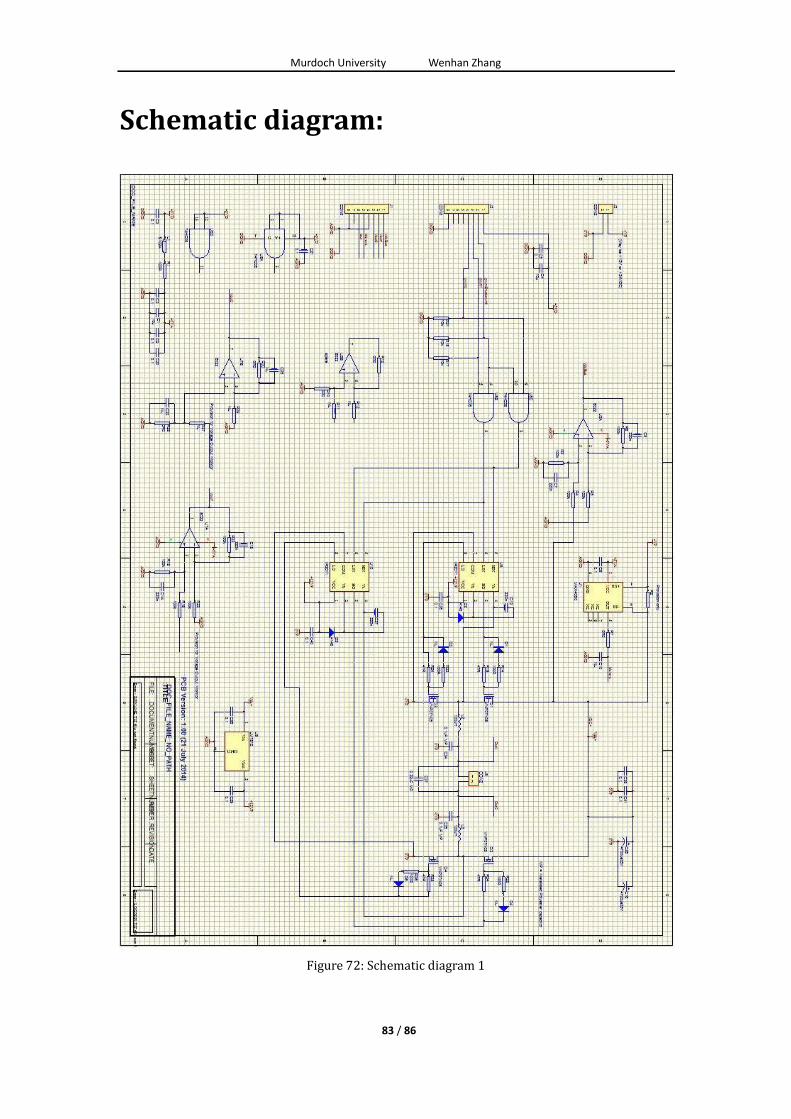
Murdoch University Wenhan Zhang
83 / 86
Schematic diagram:
Figure 72: Schematic diagram 1
t+ tt-rt-t-r:t
i=R '
*" I P,
•J
·~ p '
-j,
I ·~ =-.~ '
p ~
g
I
-
:j ·, '
. . ' 1111111111'
H-tttrH-tttt+l lliilliilliil i illiilliilll ~ lliilliilttt+-tttliilliill,•'
n -U·
.-
I:J: ., • •
-RJI p
lllllllf lr Ill'
§ _ ....... , ... •
9 •5 ' ! a
's ..
' ,_ _ 1)
•'
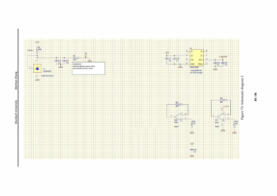
Mu
rdo
ch U
niv
ersi
ty
W
enh
an Z
han
g
8
4 /
86
F
igu
re 7
3: S
chem
atic
dia
gram
2
l\GFiq
it 101 AGND
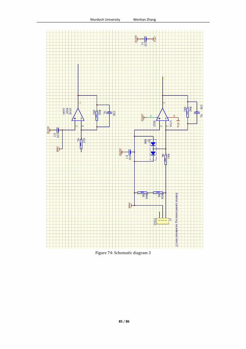
Murdoch University Wenhan Zhang
85 / 86
Figure 74: Schematic diagram 3
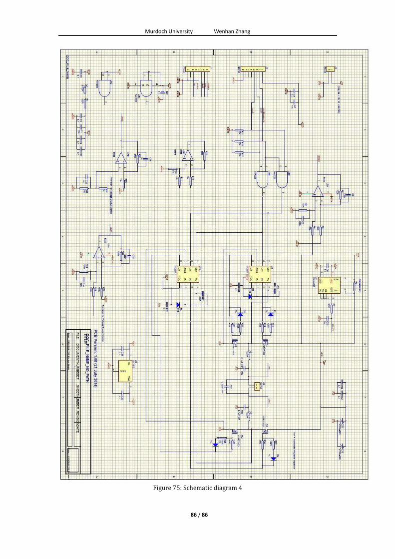
Murdoch University Wenhan Zhang
86 / 86
Figure 75: Schematic diagram 4
FRI .
'n
,H 0·
''
. -d
. ·l
I
§ •..•••.. ., .. •
~'let "iul-
•'
' ,__ 1)
·"'
' ' ' ' ' ' ' ' ' ' ' ' ' ' ' ' . ' ' ' ' ~ 1111111111111111111 11111111 l· 111111111111111111111111111 ~ 1111111111111 1111111111111•