energy efficient wireless transmitters: polar and direct...
TRANSCRIPT

Energy Efficient Wireless Transmitters: Polar andDirect-Digital Modulation Architectures
Jason Thaine StauthSeth R. Sanders
Electrical Engineering and Computer SciencesUniversity of California at Berkeley
Technical Report No. UCB/EECS-2009-22
http://www.eecs.berkeley.edu/Pubs/TechRpts/2009/EECS-2009-22.html
February 4, 2009

Copyright 2009, by the author(s).All rights reserved.
Permission to make digital or hard copies of all or part of this work forpersonal or classroom use is granted without fee provided that copies arenot made or distributed for profit or commercial advantage and that copiesbear this notice and the full citation on the first page. To copy otherwise, torepublish, to post on servers or to redistribute to lists, requires prior specificpermission.
Energy Efficient Wireless Transmitters: Polar and Direct-Digital Modulation Architectures
by
Jason Thaine Stauth
B.A. (Colby College) 1999 B.E. (Dartmouth College) 2000
M.S. (University of California, Berkeley) 2006
A dissertation submitted in partial satisfaction of the
requirements for the degree of
Doctor of Philosophy
in
Engineering – Electrical Engineering and Computer Sciences
in the
GRADUATE DIVISION
of the
UNIVERSITY OF CALIFORNIA, BERKELEY
Committee in Charge Professor Seth R. Sanders, Chair
Professor Ali M. Niknejad Professor Paul K. Wright
Fall 2008

The dissertation of Jason Thaine Stauth is approved:
Chair Date Date Date
University of California, Berkeley
Fall 2008


1
! "
#
$
%&'(
)*'
+ +
* & & &
&,&'++
-.,&
*/,&'+
+ ' ,
- & + '
+0#1*/+'+
*
,'+,+
++*

2
/+('&
& *
#+*
& & 01 *
&+,('!
' + * 2'
3 ,+ /!4 , &
+,+*
+( & , &
* , +
+( + *
& )2 3$ (
&(!*&
& (
*
# , , +!
&*&&
+,'!++
+*+,
& + 5 ,-&* !
& ! & ,
* 5 & ,

3
+*&.
&&
*
,!,!
)2 * / + '
+!* + '
+,,∆Σ6"75
! *8975* #
:"; #&+*
& ( < *=> *8975 + #
&*?".*> 4@πA8 4@
-* ( *6B )
*
;&+(&3&
+*7++(+
& ,
,*
)* Dissertation Committee Chair

Contents i
Contents
*6*6 ." ********************************************************************************** C
*6* "D ******************************************************************* :
**6 9;/ ***************************** 6
*<*6 / ***************************************************************************** 6C
*<* / ***************************************************************************** 6E
*8*6 %,, 20 21+ <
!! *=*6 +#;*********************************************************************** =
*=* D+## ************************************************************ C
*=*< ++#. ****************************************** :
*=*8 +(*********************************************************************** <<
! "
"! # <*6*6 &( ************************************************************************ <:

Contents ii
<*6* " *********************************************************** 8
$% <**6 D) ************************************************************************************** 8=
<** +?) ******************************************************************* 8C
<**< 7,?)/************************************************** =
# !$%!%
& "!$'(( )* # " '( & +, 8*<*6 !/0+!1?!# ************************************* C<
8*<* "!?# **************************************************************** C8
* -)+. ($/ #, + " #+ 8*C*6 ,))" *********************************************************** E
8*C* )+" *********************************************************** 6
8*C*< +)-)!D&# ********************** 8
# .#
&& '!( ) **
&.. /!! 0 / 1"0 / -('" 0+ 2, + 3 % ,+ # &42 . ( .
" ++ ,%$% ! -
+ ! + 2! C**6 45F ********************************************************************************* 68

Contents iii
C** ! *************************************************************************** 6=
C**< *************************************************** 6E
C**8 +!,'+35 ************************************************************************************************** 6
+ /! 2!, C*<*6 F****************************************************************************************** 6<6
C*<* )20F+,1 !#&0 #1******************************** 6<=
+ 2' %5 . C*8*6 )2 &***************************************************************** 6<:
C*8* )2 &************************************************************************ 68
C*8*< /+ ******************************************************************** 686
+ 67-%5 182% C*=*6 / ******************************************************************************************** 688
C*=* # ******************************************************************************************** 68C
C*=*< !0 "1 ************************************************************* 6=
C*=*8 *********************************************************************************************** 6=6
C*=*= ∆ΣF!*********************************************************************** 6=C
C*=*C ! # *********************************************************************************************** 6=:
C*=*E "; #/********************************************************** 6C
C*=* /************************************************************************** 6CC
C*=*: . ******************************************************************************* 6CE
. /0 .

List of Figures i
Figure 1. CMOS ft and fmax (performance analog/mixed signal devices), International
technology roadmap for semiconductors (ITRS) [1]. ................................................. 1 2''&* .......................................... 5 2<*,+,,A,* ......................... 6 Figure 4. Complex constellation diagram and trajectory for (a) constant envelope
modulation and (b) π/4DQPSK, which uses amplitude modulation for the same constellation points as (a)............................................................................................ 7
2=*&,+,&* .... 9 2C*?"* .............................. 10 Figure 7. Transmitter output spectrum showing spectral regrowth. ................................. 11 Figure 8. Direct-conversion Cartesian transmitter schematic diagram............................. 12 Figure 9. Effects of I/Q and quadrature LO gain and phase imbalance........................... 13 Figure 10. Kahn envelope elimination and restoration (EER) transmitter architecture
[19]............................................................................................................................ 14 Figure 11. General representation of the polar transmitter architecture. .........................15 Figure 12. Phase-path circuit architectures: representative techniques ........................... 17 Figure 13. Time- and frequency-domain waveform comparison: Cartesian and polar
systems. Baseband I/Q waveform with two-tone zero mean sinusoid..................... 18 Figure 14. Distortion mechanisms in polar systems: gain and phase vs supply voltage. 20 Figure 15. Common-source amplifier circuit showing mechanisms for AM-AM, AM-PM
distortion ................................................................................................................... 20 Figure 16. Representative probability distribution function (PDF) for CDMA
applications [31]........................................................................................................ 23 Figure 17. Power amplifier block diagram and schematic for a CMOS common-source
PA ............................................................................................................................. 24 Figure 18. Class-AB PA voltage and current waveforms................................................ 27 Figure 19. Switching PA schematic and time-domain waveforms.................................. 29 Figure 20. Class E PA schematic..................................................................................... 31 Figure 21. Power amplifier efficiency in power backoff overlaid with a representative
PDF ........................................................................................................................... 33 Figure 22. Efficiency versus output power: i.) conventional class B PA, ii.) class B PA
with dynamic supply regulation, iii.) class B PA, dynamic VDD with realistic loss mechanisms............................................................................................................... 38
Figure 23. Envelope tracking transmitter using traditional Cartesian architecture with a dynamic supply modulator to improve average efficiency....................................... 39
Figure 24. Time domain waveforms for VDS RF carrier waveform and power loss: fixed VDD and dynamic VDD. ............................................................................................. 40
Figure 25. Time domain envelope tracking waveforms .................................................. 40 Figure 26. Dynamic supply polar modulation system ..................................................... 42

List of Figures ii
Figure 27. Linear regulator topologies............................................................................. 45 Figure 28. Generic voltage-mode switching regulator block diagram ............................ 46 Figure 29. DC-DC conversion cells: buck, boost, and inverting buck-boost .................. 46 Figure 30. Typical battery discharge curve and power converter mode of operation ..... 46 Figure 31. Pulse-width-modulation (PWM) waveform................................................... 48 Figure 32. Fundamental and harmonics of pulse-width modulated waveform versus duty
cycle, normalized to fundamental peak. ................................................................... 48 Figure 33. Contour representation of average efficiency of the switching regulator vs
gate width.................................................................................................................. 51 Figure 34. Hybrid voltage regulator schematic: a.) Series hybrid, b.) Parallel hybrid .... 52 Figure 35. Effect of supply noise on RF amplifier output spectrum ............................... 55 Figure 36. Noise sources in RF systems .......................................................................... 59 Figure 37. Self-induced power supply noise from high supply impedance at the envelope
frequency................................................................................................................... 66 Figure 38. CMOS inductor-degenerated common source amplifier showing nonlinear
elements. ................................................................................................................... 68 Figure 39. MOSFET drain current versus gate-source and drain-source voltage.
Nonlinearities are extracted around the dc operating point highlighted in the figure.................................................................................................................................... 68
Figure 40. ! .................................................................. 77 Figure 41. D, ..................................................................................... 77 Figure 42. ,!,*
6*8G6*8*......................................................................................................... 78 Figure 43. ,
+ ........................................................................................................................ 79 Figure 44. ,,!,+
*....................................................................................................................... 80 Figure 45. Mea&+:"75 .................. 82 Figure 46. "&+*8975 .................... 83 Figure 47. ))&3'?!'+
,!&*............................................ 85 28 *!+,..................... 88 Figure 49. Model for parallel hybrid switching-linear regulator ..................................... 88 Figure 50. Two different time-domain envelope signals that share the same power
spectrum: one with peak-average power ratio (PAPR) of 10.1dB, and another with PAPR or 5.2dB.......................................................................................................... 92
2=6*,+ .................................................. 94 2=*&&#"! ...................... 97 2=<*&#"'5(
H6# ...................................................................................................... 98 2=8*&&!#"+'
+0=810=:1............................................................................................ 102 2==*&5&/!:= "#' 102

List of Figures iii
2=C*. ....................................................................................... 107 2=E*#&&+,!#"
.............................................................................................................. 108 2= *#&&&#"
*............................................................................................................. 108 2=:*+! .................. 110 2C*/!:= "#' *66D#F........................................ 110 2C6*;+05 DCSR ii /* 1&+
................................................................................................................................. 112 Figure 62. Hybrid regulator model including output capacitance ................................. 113 Figure 63. Hybrid regulator with load capacitance: efficiency versus normalized time
constant (simulation vs theory)............................................................................... 117 Figure 64. Conventional cellular phone block diagram: digital application processor,
DSP, Audio, Power management; Radio is still largely analog ............................. 119 Figure 65. Proposed digital polar architecture............................................................... 119 Figure 66. Traditional Cartesian transmitter architecture: lowpass data conversion
followed by upconversion mixers........................................................................... 121 Figure 67. π/4DQPSK and 8PSK constellation diagrams ............................................. 121 Figure 68. Input-output transfer characteristics for a 3-bit D-A converter.................... 123 Figure 69. Comparison of continuous and quantized signal levels showing error between
±½ LSB................................................................................................................... 124 Figure 70. Frequency-domain representation of discrete-time sampling process ......... 125 Figure 71. Time- and frequency-domain characteristics: zero order hold (ZOH)
reconstruction.......................................................................................................... 127 Figure 72. Signal and noise before and after sampling.................................................. 128 Figure 73. Quantization noise spectral density: a.) Nyquist-rate sampling, b.)
Oversampling.......................................................................................................... 129 Figure 74. Signal and quantization noise with noise shaping........................................ 130 Figure 75. Linear model of the noise-shaping process: quantization noise appears as a
disturbance .............................................................................................................. 131 Figure 76. Noise-shaping data conversion blocks: a.) Error-feedback structure, b.) first-
order sigma-delta modulator ................................................................................... 131 Figure 77. RF DAC: quantization of RF carrier amplitude ........................................... 135 Figure 78. Frequency-domain RF DAC with sampling images .................................... 135 Figure 79. RF DAC example implementation: binary weighted class-A amplifier stages
(current summing), as in [105]................................................................................ 136
Figure 80. Bandpass Σ∆ modulator with center frequency at 4
sf................................. 137
Figure 81. Direct digital modulation: transmitter operating as a D-A converter.......... 138 Figure 82. Cartesian RF data converter ......................................................................... 139 Figure 83. Polar RF data conversion: RF amplitude DAC with phase-modulated clock
signal ....................................................................................................................... 140 Figure 84. Upsampling to reduce spectral images, process in Pozsgay [106]............... 142

List of Figures iv
Figure 85. Digital polar modulation architecture........................................................... 144 Figure 86. Candidate polar architectures ....................................................................... 146 Figure 87. Time and frequency domain examples for full- and half-amplitude modulation
................................................................................................................................. 148 Figure 88. Pulse-density modulator block ..................................................................... 150 Figure 89. 1-Bit polarity feedforward to reduce power from rapid phase transitions... 152 Figure 90. Constellation diagram for 8DPSK with feedforward phase transition:
4
5
4
ππ → .................................................................................................................. 152
Figure 91. Polarity bit significantly reduces high frequency power in the RF clock signal waveform by smoothing phase transitions near origin ........................................... 153
Figure 92. Effect of polarity on amplitude quantization - ∆Σ process remains linear near zero.......................................................................................................................... 155
Figure 93. Error-feedback digital ∆Σ modulator ........................................................... 156 Figure 94. Example baseband 3rd order ∆Σ modulator spectrum with a notch at ±12MHz,
123 5.25.2)( −−− −+−= zzzzG ................................................................................. 157
Figure 95. ∆Σ Modulator: 1st, 2nd, 3rd order comparison, all zeros at 2.4GHz............... 158 Figure 96. Complementary class D PA schematic......................................................... 159 Figure 97. Schematic representation of class-D power amplifier with cascode output
stage ........................................................................................................................ 162 Figure 98. Current recycling scheme: excess current from PMOS drive stage used by
digital processing .................................................................................................... 163 Figure 99. Class-D PA output stage NMOS layout: gate and cascode share diffusion
region to reduce junction capacitance..................................................................... 163 Figure 100. Level shift and deadtime control ................................................................ 165 Figure 101. System-level implementation of Bluetooth transmitter.............................. 166 Figure 102. Die Photo of CMOS class D PA and RF pulse-density modulator circuits
................................................................................................................................. 166 Figure 103. Block diagram of the experimental setup................................................... 167 Figure 104. Time-domain waveforms at transmitter output .......................................... 168 Figure 105. Efficiency and output power vs supply voltage ......................................... 169 Figure 106. Efficiency and linearity&! ................................................... 169 Figure 107. Power of digital processing (pulse-density modulation, clock recovery,
sampling and synchronization) with and without current recycling scheme. Measured as power drawn from Vhalf regulator .................................................... 170
Figure 108. Measured constellation diagrams ............................................................... 172 Figure 109. Efficiency and output power vs supply voltage ......................................... 173

List of Tables i
Table I. Comparison of power amplifier performance .................................................... 32 Table II. Average efficiency calculations for the curves in Figure 21 *constant bias
current **variable bias current.................................................................................. 33 ,///*........................................................................................................................... 105 Table IV. COMPARISON OF FOMS OF VARIOUS AMPLIFIER CLASSES (DATA
FOR CLASS E, F-1, F2,3,4,5 FROM [34])............................................................ 161

1
Chapter 1 Introduction
Figure 1. CMOS ft and fmax (performance analog/mixed signal devices), International technology roadmap
for semiconductors (ITRS) [1].
# ' &
& + + + !,+ 0 1 .6975I6'J*+Figure 1'.
'.+ &
3* / "; '
, +!975 3* ,+
. ' ! !+ +

Introduction 2
,()23*,
+ )2
.*
7 3 & + , + 3
,( * 3
,,&*7
&.,+&'!
, , 3 ! I<' 8J* 7
, + &
' + ' .,
3* / , ' +
+&&
+!I8!CJ*
/ +(++ , .,
+ * +
& &!( IEJ*
& & + 0#1
.+*++
& ' , +!
++ * 2'+
+ , ! :

Introduction 3
";* )2! &+ !
+*!
)2 ! !
)2(*
*+&+.&
,,,+*
< + 3 )2 * +
& &+
&*
8+-)2
* , .&!(*
#!?!
.+)2!,+*
!&&' &,
3*
=,,+!&
*,,
& & +&* ' , !
&' + & , + & ,,
Introduction 4
& 3 *
+,&5+*
C!!)2+
# !!)2 &* &+ ,
&35!
* # &+ & &'
, !# &* C*= !
*6B ) *8975*
3+&<>&*

5
Chapter 2 Transmitter Fundamentals
"+& , ,
+&*#
++&$
, &* & , ,!
,+,.,!&'!
&'+*7'++
+ ' , ' '
*
#+2'+&
+ & * /+,
' 3 &
+& , * &
& , +! * , &
' * )2 -

Transmitter Fundamentals 6
and Q(t) baseband signals and upconverted using quadrature local
oscillators:
)cos()()sin()()( twtQtwtItv CC += ' 061
+ )(tI !&' )(tQ 3&' Cw
)23*
)2-,
)2 * ' )2
+
[ ])(cos)()( ttwtAtv C Φ+= ' 01
+ )(tΦ IEJ*
0#"1 0"1
* /' .
++*
2.1.1 Complex Modulation

Transmitter Fundamentals 7
Figure 4. Complex constellation diagram and trajectory for (a) constant envelope modulation and (b)
π/4DQPSK, which uses amplitude modulation for the same constellation points as (a).
,+,&
+3* , ,
'+. , ,* /
2<01',(0@1&&
,+ + 6 * / @' 6 , ,*7&,*
2<0,1+304#"1+8,&*
+ +, , & ,' * 2 <*
+4#"+6C,8!,,*7
6C!4#"+ &
,*'!&
&,I J*

Transmitter Fundamentals 8
/ , - ,
*Figure 401+&
, ,'+*
,,&-'
Figure 40,1* 7' - + πA8 4@
' & +,
,* /πA8 4@ '
&, 5$&
,AA75* πA8 4@
5$-&
$ )B*6 I:J* &
, , , *
,+ ,
*#+&+&Figure
40,1 & Figure 401 & , ' Figure 40,1
,
,+,*&&+
,(+I '6J*

Transmitter Fundamentals 9
2.1.2 Digital Modulation Limitations
+
,* /',&+
*F,&&
&*+2=',+,
&3&*#
,!&!0?"1*?"
!!33,,
( )
m
N
je
V
VN
EVM∑
== 1
21
* 0<1
/0<1'&,',&' ,*(&
,* ?"3&+
'+ +,+<><=>* 2
*66A=8"A'?"&6,01,,+=*C>I6J*

Transmitter Fundamentals 10
?"3*F
+ , &' +
& + ,
* / #"!#" 0!& 1
#"!" 0!&1' + 2C I66J*
#"!#",&
* # #"!#" 3 !6
)2 I6' 6J* +
*
&&&$
* #"!"
$
' , , &
& & I6<J* + ,
*

Transmitter Fundamentals 11
Figure 7. Transmitter output spectrum showing spectral regrowth.
+ , *
,3 #"!#"#"!"+
3*
*#
+Figure 7',+
( * ( +
, 2 & + - ' +
& !. "# I68J* +
, 3 ,
* / &
*&
!,&*
#& 3 ,('
, +DI6J*

Transmitter Fundamentals 12
Figure 8. Direct-conversion Cartesian transmitter schematic diagram.
+ +
$061*/
, & ,( /A4 , &' +
,,,-*+Figure 8
& * +
,,' & )2 *
+0#1'+&)2
*
2.2.1 Cartesian Transmitter: General Operation and Issues / ' . - + ,
&*&,+!
,, +
(* #!& 0 #1& &
* # 3 . /A4 +
0:1*&&

Transmitter Fundamentals 13
+
0#1*#&+'&)2+
=K&*
& , & )2 '
,,3,)2*7+&'
$ #'.'#$& '
,I68'6=J*/
#
+*=+#
+ ? &* ; #
,3'I6=J'?&'I6CJ''I66J*
Figure 9. Effects of I/Q and quadrature LO gain and phase imbalance.
; + D; (' D; '
,3D;*+Figure 901'D;(
3,
/A43D;I68J*/,3D;+

Transmitter Fundamentals 14
& / 4 * ,
&5 Figure 90,1* /Figure 90,1'D;
( & & & 0'1*
, 5 + .
3D;5*/,,,D;(,
/4,,* 3 I6EJ +
*
D;,' &*
&! 0?;1 D;
3#*#,
+,,(?;'-
(*D;&,?;3
D;?;&+&&'
&D;I6 J*
Figure 10. Kahn envelope elimination and restoration (EER) transmitter architecture [19].

Transmitter Fundamentals 15
Figure 11. General representation of the polar transmitter architecture.
*
+&
22 )()()( tQtItA += ' 081
=
)(
)(arctan)(
tI
tQtφ ' 0=1
+ )(tφ !*
#-,+
,&''&+
/A4,&)2* 0810=1
φ &*F081
0=1,&,
* $ +?"
$+,,

Transmitter Fundamentals 16
!&* +
*
2.3.1 Polar Implementations @&0)13.
+ .
)2I6:J*/@3'+Figure 10'.
5)2'&#&
+ & * .+
&*#@!&
&*
#'!' ''2IEJ'+,
* ! &
, & #' )
* # . 3+,), IJ*
@ 3 , ,
'I6<'6!=J*
Figure 11+5&+
&*/Figure 11'#+
&,! 0?9#1* / ' +
&,*
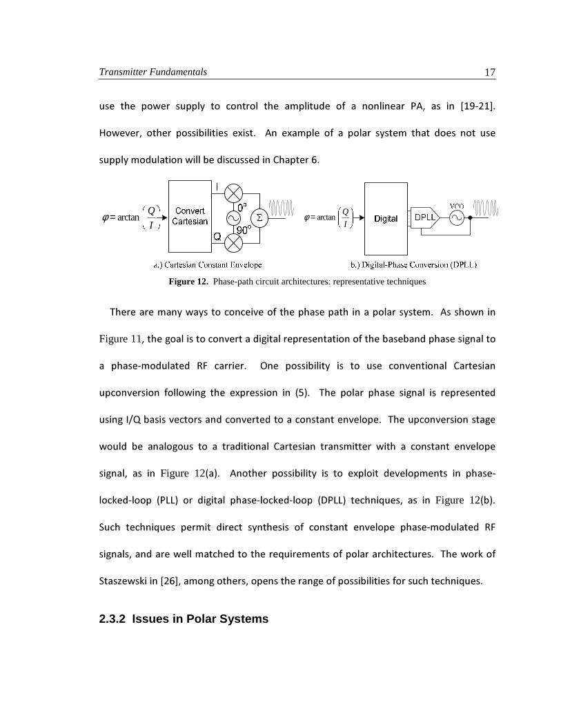
Transmitter Fundamentals 17
+ #' I6:!6J*
7+&' , .* # .
+,C*
=I
Qarctanφ =
I
Qarctanφ
Figure 12. Phase-path circuit architectures: representative techniques
+&*#+
Figure 11'&,,
! )2 * ; , &
& + . 0=1*
/A4,&&&*&
+ , + &
' Figure 1201* # , . & !
(! 0DD1 !(! 0 DD1 3' Figure 120,1*
3 & ! )2
'+3*+(
5+(ICJ'',3*
2.3.2 Issues in Polar Systems

Transmitter Fundamentals 18
Figure 13. Time- and frequency-domain waveform comparison: Cartesian and polar systems. Baseband
I/Q waveform with two-tone zero mean sinusoid.
,*+,
* + Figure 13'
+ , & +,
+3&* Figure 1301+!
+&,,
)3cos()(
)4sin(2
1)2sin(
2
1)(
tftQ
tftftI
R
RR
π
ππ
=
+= 0C1
+6*"75*+&0C1,,+ & 3.* # + Figure 130,1' +

Transmitter Fundamentals 19
,,,6"75'6*="75'
"75*
+ ' Figure 130,!1 +
+, 3 ,&* !+&
&&,&* !3
5* ! + 3
3 ' + Figure 1301*
3 3 + Figure 1301* 7'
/A4 &'
Figure 1201*,+
+-
*,6 )2 * / ' & +
5* 7+&'+
5 &'
'3+*
+,&!,+
*#+,+
'
* / ' + ( ,+
.6"75&?",+3IE' J*

Transmitter Fundamentals 20
Figure 14. Distortion mechanisms in polar systems: gain and phase vs supply voltage
Figure 15. Common-source amplifier circuit showing mechanisms for AM-AM, AM-PM distortion
#-*/'#
+ . & ,- !
I6='6CJ* / !
'#,-&*+
Figure 1401' #&&* / '
+ !";&' &
& ! * Figure 15
+ & * & Figure 1401
AV
VDD
Phase (rad)
VDD
a.) PA voltage gain vs VDD b.) Phase of RF carrier vs VDD

Transmitter Fundamentals 21
";#.,.'#"!#"
I6<J* 9 . "; ! ,
,*Figure 140,1'+&)2*"
& & & &!
-* & ,
& & * # +
&'#"!",,#
'!*
,!&$+(
',6 I6<J*(#',"' IEJ*,,+,
+ Figure 1301 # '
*
#-+,'
+ * & + &
& & + & * / ! #
' + #* '
.+)2,&)2'
)2 I:'<J* , , &

Transmitter Fundamentals 22
('?"*8,,'
3&*
2.4 Power and Energy Efficiency: Polar and Cartesian Architectures
# ?" ( ' +
+*/,
+ ,( , +
3 #* + & + ,
&,' # # , ,
#* , ,3 $ #
'+,
supply
loadavg E
E=η , 0E1
+ & +*0E1
&',,*

Transmitter Fundamentals 23
2.4.1 Typical Use Patterns: Probability Density Function (PDF) of Transmit Power
0
0.5
1
1.5
2
2.5
3
3.5
-50 -40 -30 -20 -10 0 10 20 30
Output Power (dBm)
Pro
bab
ility
(%
)Urban
Rural
Figure 16. Representative probability distribution function (PDF) for CDMA applications [31].
/ , '
. +* / ' + &
-.,*
+ & + , ' &
+ +* (+
!,!+I<6J*
Figure 16+,,&+ "#
,&*.+<'+'
, &+ =!66* '
.+,&&*
&, 2
Transmitter Fundamentals 24
∫∫
∞
∞−
∞
∞−
⋅
⋅=
LLsupplyL
LLL
avg
dPPPPg
dPPPg
)()(
)(
η , 0 1
+% +&0.!.Figure 161' )( LPg ,,
' )(sup Lply PP ++% *# &+ &,,
&(*
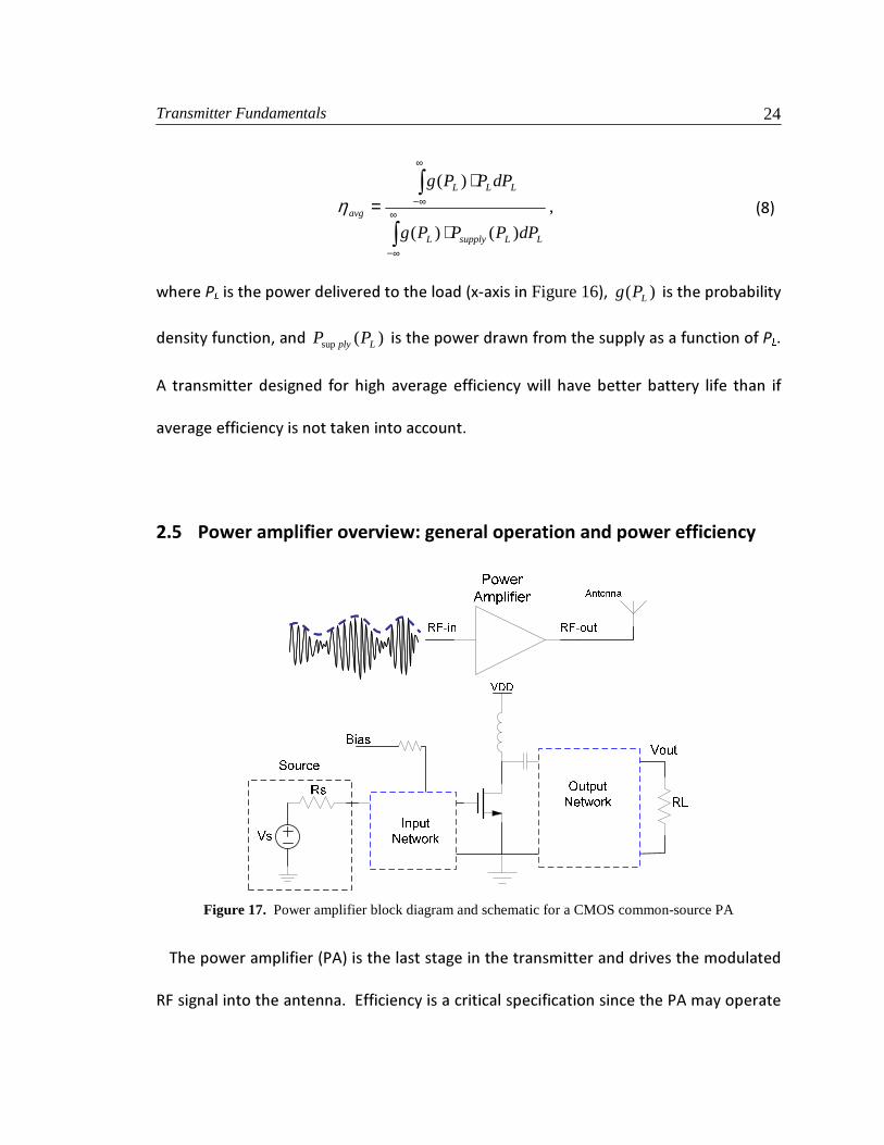
Figure 17. Power amplifier block diagram and schematic for a CMOS common-source PA
+0#1&
)2*#

Transmitter Fundamentals 25
, + ,( * ;
#'' #* +(
,+*
,- +( ),' I' <J' ' I66' <J' @'
#(''I<<'<8J')'IEJ'.I6'<=J'
L+'I<CJ*/'+&,&&+
#'&'+&
*
2.5.1 Power Amplifier Operation
Figure 17+";+*
+";&',&&
Figure 17 + , 9 ' ///!?
9#'9F'/"7&*
+ + +(
+(* +(
# & '+
3!.*/&+)2
#'&3+I<EJ*
+( '
Transmitter Fundamentals 26
'#3+.
&I6J*
/ # &
#* /''
& + * D
+( D! +(
IE'6J*)+(,
& , + & * ;
+(+,&
+&+&";*#(*I<<J
+(
,+!";#'&
*D*+#
++&'&.+&I< '
<:J*
2.5.2 Linear Power Amplifiers: Class AB

Transmitter Fundamentals 27
Imax
Vdsat
VDS
IDS
180o<Φ<360o
V
DS (V
) ; I
DS
(A)
Figure 18. Class-AB PA voltage and current waveforms
+',
&&''+(
* #' #' ' + '
*
' ''2!
' ,
*7++,#&
#*
Figure 18+&+&##* &
&',$
ML,+=>6> * ##'
' ! + I8J* #
3 &+! ' chokeL
Figure 18*+(+

Transmitter Fundamentals 28
&.*'
&',+<C0#16 0 1* & + + &' DSDSloss VIP ⋅= *#+
ply
Ldrain P
P
sup
=η , 0:1
+% +& % ++ * +3&#',
&#*
# ' Φ '
&+'5DD
odrain V
vK
ˆ=η , where
ΦΦ−ΦΦ−Φ=
2cos
22sin4
sinK
061
+Φ 26 ' ov
&&'η#I6J*###
* => # +0360=Φ DDo Vv =ˆ * . E *=> + 0180=Φ

Transmitter Fundamentals 29
DDo Vv =ˆ *061#*/'
'Φ '5'6>0'
+ 5 Φ 51* / ,
, ,
!& +& & &
*#'061'+
$+&'+
, * + & .
+*
Figure 19. Switching PA schematic and time-domain waveforms
2.5.3 Switching Power Amplifiers: Class E example
IDS
V
DS (V
) ; I
DS
(A)
VDS
VGATE VDD
a.) Switching PA schematic
b.) General VDS waveforms
c.) Class E VDS - IDS waveforms
Constrained by output network
VDS (V)
Constrained by switch
time
time

Transmitter Fundamentals 30
+ + &
,&&+*&&&
MLML
* &+&'+
&++6> * %
+#!#
&,&*
Figure 1901+";+#*&
#&'.&&
,+*+Figure 190,1'+&M'L
! & 5* & M'L !
& , +(*
+( 5 + , & & +&* /' &&+!& 5'
& 5 & + 0N?1* + ,
5+&&*

Transmitter Fundamentals 31
Figure 20. Class E PA schematic
# & , 5 & + !& $ *,
)2+' I='86'8J'+&' I86'8<J* +
Figure 1901'!&.5+&*
Figure 20+";#'I8J*&,&
, &* ! &&*
+('
+IE'6'86J*+(!
&+&-+
Figure 19 01* ! +(+ +
,&5+5&&
+*/,('I86J'
+.&+(
c
L
c
L
w
R
w
RL 1525.1
16
)4( 2
≈−= ππ, 0661
LcLc RwRwC
11836.0
1
)4(
821 ≈
+=
ππ, 061
L
DD
L
DDL R
V
R
VP
22
25768.0
4
8 ≈+
=π
, 06<1
Transmitter Fundamentals 32
+ cw 3''' Figure 20' +&*
# +,( + ! & .
&, ,* / ' DDDS VV ⋅≈ 56.3max *
, , & , !& ,(+* / ";
. ,(+ , - &
&* ( & + , +
. + & &
&*
class A class B class E
Peak Efficiency 50% 78.50% 100%
Supply constrained output power (W) (VDD=1V, RL=1Ω) 500mW 500mW 577mW
Breakdown constrained output power (W) (VDSmax=2V, RL=1Ω) 500mW 500mW 182mW
Table I. Comparison of power amplifier performance
Table I*+##* 2
&' , +
#*7+&'&,(+&&'
+ + ' +* ,(+ , + & 5!
!* &(&
5 ' + &

Transmitter Fundamentals 33
( !< & "; IEJ*
7+&' , "; ! + ( &
3,'+,-!$&
+(&*
2.5.4 Efficiency in Power Backoff #*8*6'.+',
,- + 5 , ,,
*#&,
,3&+*
0%
1%
2%
3%
4%
5%
-60 -50 -40 -30 -20 -10 0dB(Pout) - dB(Pmax)
Pro
bab
ility
.
0%
20%
40%
60%
80%
100%
Eff
icie
ncy
class E
class B
class A
Figure 21. Power amplifier efficiency in power backoff overlaid with a representative PDF
18.21%14.46%0.78%* / 9.2%**
Average Efficiency:
Class EClass BClass APA Class:
18.21%14.46%0.78%* / 9.2%**
Average Efficiency:
Class EClass BClass APA Class:
Table II. Average efficiency calculations for the curves in Figure 21
*constant bias current **variable bias current

Transmitter Fundamentals 34
Figure 21 + #' '#
+*+5.+,
&* & + &
,&+&0$
. 1* # & 2
&+&*/.'+
,+(+* # + &'+
6>*
. 0 1 &', 2*
& & Figure 21 +
Table II* #& +( *
2'&&
(*2#+,'
*Table II+
*/',(&
,+*
++(,(&
3 + , & & *
'++!+ &
& + * + + &

Transmitter Fundamentals 35
( # ' & &
,* + & +( 8 = + ,
, * C+
, & & ,
+*
36
Chapter 3 Power Management for RF Transmitters and Polar Systems
+ +
* '+,-
I6'88J* 7
& * + &
,,,'3&,
* 7' + , &,
.+&
I8=' 8CJ* +
+ ' + 0#1'+ ,
'&*
+ &
+ 3* + , +
','+,
# &* + & '
+ ! &*
+'

Power Management for RF Transmitters and Polar Systems
37
+&+-,&'
.*
3.1 Motivation: Efficiency
#'++++
, 3 ,, *
&+&,,,+(+&'
, 2*
'+#+.&+&
,&&'&
,,(*3#
*/*<+,
+# 3
@)'+ Figure 10* 7+&', +
,&*

Power Management for RF Transmitters and Polar Systems
38
0%
1%
2%
3%
4%
-60 -50 -40 -30 -20 -10 0dB(Pmax) - dB(Pout)
Eff
icie
ncy
0%
10%
20%
30%
40%50%
60%
70%
80%
90%P
rob
abili
ty
ii.)
iii.) i.)
Figure 22. Efficiency versus output power: i.) conventional class B PA, ii.) class B PA with dynamic
supply regulation, iii.) class B PA, dynamic VDD with realistic loss mechanisms.
Figure 22 #+ +
*+0.!.15(+'+
#&.πA8'E *=>* #+ '
+&)2*&
+&'?'.*&+& #+
*/!&'+,
0**
πA8 4@ Figure 4' 4#"'#@'
@1' & +
&*
& *1 ,
$+,

Power Management for RF Transmitters and Polar Systems
39
* ;&'Figure 22+&
+'++'+#
(, 2*2&'&C*=>
68*8>&*8>&*
&,3&+
&*
3.1.1 Envelope Tracking System
22 QI +
Figure 23. Envelope tracking transmitter using traditional Cartesian architecture with a dynamic supply
modulator to improve average efficiency.

Power Management for RF Transmitters and Polar Systems
40
Figure 24. Time domain waveforms for VDS RF carrier waveform and power loss: fixed VDD and dynamic VDD.
Figure 25. Time domain envelope tracking waveforms
VDD
VDS
PLOSS
time (s)
VDD
VDS
PLOSS
time (s)
a.) Fixed VDD, low amplitude class B b.) Dynamic VDD, low amplitude class B

Power Management for RF Transmitters and Polar Systems
41
&( &&&& #' (
&' & * 3
+ + Figure 23*
&+&+&&
&*/&'+,&
&&+&$+'
+Figure 24*/&+*/
+ & !
&*/&-&&'
+ & & ( * ".+ &
&-&&
+ # * / . # & +(
' &
, I ' <J* , ,,'
&)2#I6J*
Figure 25+.+&&(
* Figure 25 01+)2&+&
. *<** . ? 6*?' + .' *= 6*=O* Figure 25 01 + . ?* 7'? )2&?5+#$&";&+
Power Management for RF Transmitters and Polar Systems
42
, * Figure 25 01 + )2?+&* )2 + +?' , , & . ,& ?&*++.?',+,&*.& ( +(7* I6J'
* IJ' * I8EJ I8 !=J* ;
. # & * / I J'
*&(;2 "+&,+
"75&,+6:>! >*
3.1.2 Dynamic Supply Polar Modulation
22 QI +
Figure 26. Dynamic supply polar modulation system
, + +
* # *<*6' +#& ,+
)2+&+

Power Management for RF Transmitters and Polar Systems
43
( ))(cos ttwVv cDDRFO φα +⋅=− ' 0681
+ RFOv − )2+&' )(tφ !&)2'
α ,+ *Mα L ',
#'&'IEJ*
+2C*
,,' ( @ 3
26*&!#*
& +
& * # *<*'
*/
#"!#" #"!" '
,+?"*&
,++&*
& & , #
#0,1* "
+(3+& 5+#'
,!&*+
-&#I6<'<'8J*
&&,*

Power Management for RF Transmitters and Polar Systems
44
#,&&+&
&* %( ' & 6> *
+ & , (
+ ,(' + & *1 2 * 7+&'
+ , ,
,+ * ,+ ,+
& + 3* F +
#I<J*
*
+ + & I6J I=6J'
&#+6<"75+&*

Power Management for RF Transmitters and Polar Systems
45
-
+ Av VDDLoad
Vin Vout -
+Av VDD
LoadVin Vout
a.) Generic linear regulator b.) CMOS linear regulator
Figure 27. Linear regulator topologies# & ' ' &
,* +Figure 27' &&
& .&* / ";. Figure 27 0,1'
";&&*
/ "; & .
.&* &
,+'+''
I=!=8J*&&
,+$,
*7+&'++'
DD
outLR V
V=η ' 06=1

Power Management for RF Transmitters and Polar Systems
46
+ LRη *(
& + & *
3.2.2 Switching Voltage Regulators
Figure 28. Generic voltage-mode switching regulator block diagram
Figure 29. DC-DC conversion cells: buck, boost, and inverting buck-boost
Figure 30. Typical battery discharge curve and power converter mode of operation
2
3
4
0 1 2 3 4 5
TIME (H)
CE
LL
VO
LT
AG
E (
V)
Li-ionbuck
boost
Li-ion
Vout

Power Management for RF Transmitters and Polar Systems
47
+,,+'
, 3 . & & *
+Figure 28+'&'
&& &*#
-+&&*
, + &
&!*.+Figure
29 + 0,(1' 0,1' + 0,(!,1
&* ;0,(1'
+ ! & I==!=EJ*
*(,(!,&
,* (&
+ +' ( ' , 6>
* (!, & , & &'
, ,++ &, &* +
Figure 30',&,&3&',(!+
& +* / ,& , &' ,! *
Power Management for RF Transmitters and Polar Systems
48
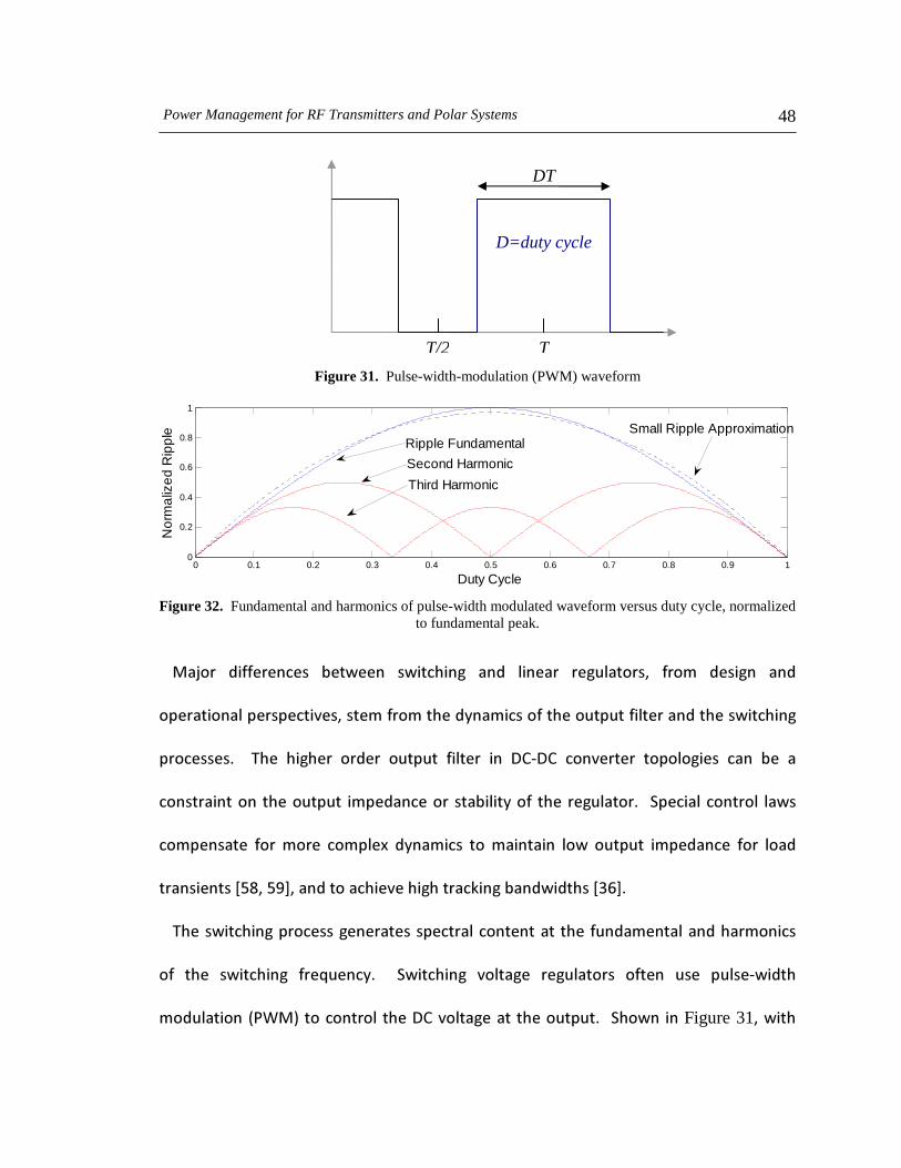
Figure 31. Pulse-width-modulation (PWM) waveform
0 0.1 0.2 0.3 0.4 0.5 0.6 0.7 0.8 0.9 10
0.2
0.4
0.6
0.8
1
Duty Cycle
No
rma
lize
d R
ipp
le
Ripple Fundamental
Second Harmonic
Third Harmonic
Small Ripple Approximation
Figure 32. Fundamental and harmonics of pulse-width modulated waveform versus duty cycle, normalized
to fundamental peak.
"- ,+ + '
&'+
* ! & ,
, * +
. +
I= '=:J'&(,+I<CJ*
+
+ 3* + & !+
0"1 &* +Figure 31'+
DT
T T/2
D=duty cycle

Power Management for RF Transmitters and Polar Systems
49
"' + +&
+&* "' + *
&+35
,& ! &* 7+&' +
+& &* 2!
"+&:
⋅⋅−⋅+= ∑∞
=1
)cos()sin()1(2)(
n
swn
in n
tnwDnDVtV
ππ
, (16)
+.&"' sww +3'
' ,*
&+2<*
,+ . , +
&* +,
,+,.+)2+
*+(+,&
0?;1'**6',I=J*
, +'+&!
$&+#*,
&.+,,8*
+
* 5

Power Management for RF Transmitters and Polar Systems
50
+ +
*9',&(,+
'+,&./A4,+I6<J*
' + 3
+* 9'+3+
+ & * ) I<CJI8=J,+
+ 5 + & 0+ .
1+
fswERIP GOrms ⋅⋅≈ 2min 2 ' 06E1
+ rmsI swf +3*7' GE
&+'O
O GR
1=
& +* 2 "; + &
3,+
)(1
minondsTDDO VVVCox
lG −−−= µ , (18)
2min DDG CoxVlE = , and (19)
swG
Ormsopt fE
RIW
⋅⋅
=2
(20)
+ minl '&' µ ,'Cox .' DDV

Power Management for RF Transmitters and Polar Systems
51
&' ondsV − &!&+*/(20)'
optW +&+*/+
' . &
&*
5455
5556
56
56
57
57
57
57
57
58
58
58
58
58
59
59
59
59
59
60
60
606061
NMOS Width (mm)
PM
OS
Wid
th (m
m)
1 2 3 4 51
2
3
4
5
Power Converter Average Efficiency Contours
Figure 33. Contour representation of average efficiency of the switching regulator vs gate width
3 06E1(20)&,5+
'+ rmsI * / '&
*/' 2,
5+*)I<CJ,+&
5 + .& *

Power Management for RF Transmitters and Polar Systems
52
5 + Figure 33 ="75 ( ,+
6* . + *6 ";* 7' & +
+&F";";+&*
2#&5&.
&* #& + +&C>&
& ++ ,+ ( +* & 5
,0";&15
(+ &* . , ,
'(*
3.2.3 Hybrid Voltage Regulators: Introduction
Figure 34. Hybrid voltage regulator schematic: a.) Series hybrid, b.) Parallel hybrid
#',&,+
* 7, &,, +
'' +'*

Power Management for RF Transmitters and Polar Systems
53
+!,
!,'+Figure 34*
, + & +! 0D ;1
'+&*+-
&+ & $
++!*"5
&&++D ;*/
' +!!-! 0))1
+*
'&&&*
,+,,(&
&,&&*#
,+'&#&*/
'#&,'
+(!!&+0#)1'ICJ*
!,&++
*/.'&+'&
&*+'
&'*
/ ' + 0& 1
+ 0 1* &

Power Management for RF Transmitters and Polar Systems
54
,-&' + * /
.'+ &
I 'C6'CJ*&,
* +
30 1*/.3
+!ICJ*/='
+,5!
,,!*)+,
! & +-,
&'&' &IC<'C8J*/
' ( = +
*;+'+++
&(*

55
Chapter 4 Power Supply Noise Analysis for RF Amplifiers
Figure 35. Effect of supply noise on RF amplifier output spectrum
/'++-)2
* & +3
,)2*#&'(
+ (+ , +
* ?! 0?;1 &
, & 3! 0&1
, & & I=J* ++
+ * 2 0681' # &
,++)2*
P(dB) P(dB)P(dB)

Power Supply Noise Analysis for RF Amplifiers 56
# ' . , + ?; # ,
+ & &!&
*
7+,-
)2* D# &&'
* 7+&'
& *
"++.+)2
*.,&(
3 * 2<= +
3.+)2$)2
,'!,')2-
,I:J*
+(I:JI<J-
+(";!'+,";
#'#'#*+(&
('(++,
&* ? +
. * . !
, ! & 3
*',

Power Supply Noise Analysis for RF Amplifiers 57
IC=J'5ICCJ',,,3I6=J*
,. /"<&<', .
*
+ , ";
+0#1*
8*<!+
* & ? &+
.!)2+* 8*8
, , 5
"; * 8*= ?
,* 8*C
. * + ! 9
:"75,+*8975*
/.&'? +
&*7,071
3 , ,' +
##& 0# 1!!01
ICEJ*,3&
+&.'&,
Power Supply Noise Analysis for RF Amplifiers 58
3 3 (+ * 7'
+ , * ( ,
,,+
- + 0#)1' + + !
+&* / ' ? 0?1 &
&
• ? , +(+ 0& +(1*
• ? ( & . 3 ,& & '+&*
• &0+,+!+&1
• ?+!,,,&' IC J' + 3 +*
Power Supply Noise Analysis for RF Amplifiers 59
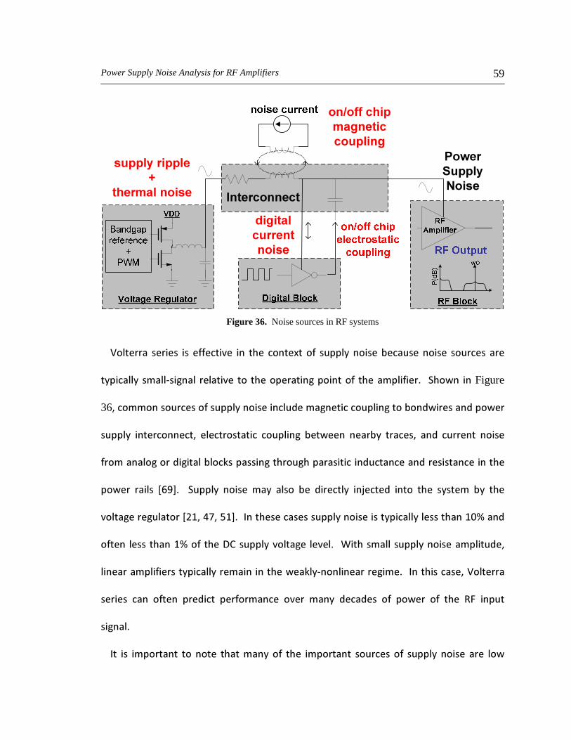
RF OutputDigital Block
on/off chip magnetic coupling
noise currentdigital current noise
RF AmplifierVDDBandgap reference+PWMVoltage Regulatorsupply ripple
+thermal noise on/off chip electrostatic coupling woP(dB)
Power Supply Noise
RF BlockInterconnect
Figure 36. Noise sources in RF systems
? & . ,
! & * + Figure
36',++
' ,+ , '
,(
+ IC:J* , - ,
&I6'8E'=6J*/6>
6> & &* '
+(!*/'?
& + )2
*
/ +
Power Supply Noise Analysis for RF Amplifiers 60
3&)2*,
+3', &* +3'
. ,, !,!,
3* /'?,
& + 0#1 +
- 0))1* , .5
+&&'+
?"#)3*
!
+.+)2,&,
* +
&
*#3,+(
,* /, +3
5 * D+ 3
, , ,
,*
# ! ,
* / )2 &'
,5+++

Power Supply Noise Analysis for RF Amplifiers 61
I6'EJ*,&
' , ,+ & &
& * , +
+,&*/'
, 5 &
+*5,
'',++'...
...
...),(
303
20201
212
22111
330
22010
++++
++++
++=
vddvddvdd
vddinvddinvddin
inininvddinout
SaSaSa
SSaSSaSSa
SaSaSaSSS
' 061
++-+ # & P ' ' *7', + ' , + ' , ,+ */+ )cos( 0tvS iin ω= '
+ )cos( tvS Ssvdd ω= '
,+, Sωω ±0 ''
.2
1)( 110 SiSout vvav =± ωω 01
/',
,!,+01* # 01'3 &,
Power Supply Noise Analysis for RF Amplifiers 62
,
* / ,
+! ' + &
+(+'.*,
+,'3
.,' ⋅=sva
adBdBcSideband
12)(
11
10 * 0<1
.' + .
',,0<1*/
, !
* ' ,
,,!!'+-0))1I8J*
/+(++)))2
=11
102)(
a
adBdBVPSRR * 081
11
102
a
a &,.0<1,,
* & 081 *
081
*/,061!081
Power Supply Noise Analysis for RF Amplifiers 63
+! * F. + + , +
+3*
? , 5 ,& +
*#+('+
* ?
' !&
' ',+
∑∞=
=0
))(()(n
n txFty ' 0=1
+
...)()...(),...,(...))(( 111 nnnnn ddtxtxhtxF ττττττ −−= ∫∫ ∞
∞−
∞
∞−
* 0C1
/0C1' ),( 1 nnh ττ L (+?(*!'+&0C1'(+? ? ICCJ* 2 & 0=1 0C1' ?
5 & *
?(,3??
I6=' C=' CC' E6J* /
? 3 ' ),...,,( 21 nn jjjH ωωω '

Power Supply Noise Analysis for RF Amplifiers 64
&
3 ICCJ* " , ?!
..!3I6='
6C'C='CC'C 'E6!ECJ*
. ! ? ! , ,
. & 0C1 *
,,+'!
,*#061'
, ,. ,+ )2 *
!?',
,' & ,
.*
∑∑∞
=
∞
=
=0 0
21 ))(),(()(m n
mnout tvtvFtv 0E1
...)-()...-()-()...-(),...,())(),(( 1212111121 nmnmmmnmmnmn ddtvtvtvtvhtvtvF +++
∞
∞−+
∞
∞−∫∫= ττττττττL 0 1
Looo Looo Looo++++
++++
+++=
221122
21212111
3203
2202201
3130
2120110
),,(),,(),(
),,(),()(
),,(),()(
SSjjjASSjjjASSjjA
SjjjASjjASjA
SjjjASjjASjAS
cbacbaba
cbabaa
cbabaaout
ωωωωωωωωωωωωωω
ωωωωωω 0:1
? +

Power Supply Noise Analysis for RF Amplifiers 65
, + 0E1' + 0 1 !
&0C1*/0 1'?(' + ' ? * / 3 ? ,+ 0:1*
7?'-*ω3&,& 3 * QR
3
3 * 0:1
,+IE8J* /0:1'01?+*,* , * / , ? 0:1 061*
0:13
+(*

Power Supply Noise Analysis for RF Amplifiers 66
Figure 37. Self-induced power supply noise from high supply impedance at the envelope frequency
#,,#*#+
2 <E' + )2
&*/'&+*
,++*
&!?+,
+! 20A ' 30A '*!,
,',&+
,&3*/+
3+#*/+(
+ *
11A * / , ,
'!,5
* / ' 11A

Power Supply Noise Analysis for RF Amplifiers 67
,,*
/+('+F!,(,.+0
*2<=<!
+&*
, '+
*/++ω'++ω'+ , ω ω' + ,ω ω ω ω*))+
),(
)(2
011
010
SjjA
jAdBPSRR
ωωω
= ' 0<1
+ , & ( .
* / , '
' ),(),( 12112111 ωωωω jjAjjA ≠ * /&' , +
' 3
,* # ?
, +3 IE6J* #
+&',
&.*

Power Supply Noise Analysis for RF Amplifiers 68
Figure 38. CMOS inductor-degenerated common source amplifier showing nonlinear elements.
DC operating point
Typical operating
region
Figure 39. MOSFET drain current versus gate-source and drain-source voltage. Nonlinearities are
extracted around the dc operating point highlighted in the figure.
/ ! - ' +
, ";+ 6 * 2 < + ,
,+)2(*!,
)2 , #' +!

Power Supply Noise Analysis for RF Amplifiers 69
* 2 < + - ";
* / .'
01' 0 !,( -
01*;,,!
'&&*
F 2< +. /"<&<
*2<:+
& ! ! &*
+
gsv dsv */' dsgs vv × *
. ,+
*2<:
& /!? * +
' , & /!? , '
& ' & * ? .
& 01,+&&&*
++
!3I6='6C'ECJ*.
& - ,

Power Supply Noise Analysis for RF Amplifiers 70
LL LLL++++
++++
++⋅+⋅+
−−−−
+++=
33221
33
221
221
21211
33
221
33
221
32vdb
dt
dCvdb
dt
dCvdb
dt
dC
vdsgovdsgovdsgo
vgsvdsgmovgsvdsgmovgsvdsgmo
vsbgmbvsbgmbvsbgmb
vgsgmvgsgmvgsgmid
*0<61
/ 0<61' + ' ,
'! - ' ' *
502< 1*.!&'I6='
CCJ'6A6A<<+*
&?0:1'3+
&3.0<61',+
*+,I6='CC'E8J*#3?
+ '
+'.',&*
! , + +
* 2 ! 2 < ' +
&'

Power Supply Noise Analysis for RF Amplifiers 71
&',(3*
%'?0:1,+
∑∑∞
=
∞
=
=0 0
21),...,(i j
jika
nijn SSjjAS oωω ' 0<1
+ nijA
*2' &+
* / ,
& * & ,
''
* ' & 3
'.,&I6='CC'E8J*
/' 1ijA +,
'+ 2ijA + , &
&*2< &
)()()(
0
1110
aaSa jK
gmjyjA
ωωω −= '+ 0<<1
)()()()( 11110 LXSLXa yyyyyyygmbgmjK ++⋅++⋅++=ω * 0<81
+ * 3 &, 3 ICC'E8J*
2 & ' ( ) 1)( −= SaaS Ljjy ωω * !

Power Supply Noise Analysis for RF Amplifiers 72
' & ω* / 0<81111 )( Cjgojy aa ωω += ! ,
'1go ' ' 1C 0<61* !
1)()( −= Caax Ljjy ωω +
( 'CL *
1)( −= LL Ry * / 0<81 )( ai jy ω ,
iy .',,
ω* 2++. 3ω.*+
0
1101
)()(
K
yygmjA LX
a
+=ω ' 0<=1
0
111210
)()(
K
ygmbygmyjA SX
a
+++=ω ' 0<C1
0
201 )(
K
yyjA LX
a =ω * 0<E1
/0<=1!0<E1'.''0<81'&3'ω'*20<=1 0<E1 3&,ω+ 3 ' ω' + 0<C1' ω 3 )2 ' ω* . 5 ,& ,+

Power Supply Noise Analysis for RF Amplifiers 73
*
? 5 . ,+
, 111A */' 1
11A ,)2
[ ])(),(),()( 00111 SSSoout VsVijjAv ωωωωωω o=± ' 0< 1
+ ω ω 3 )2 '&* # & ' 1
11A
, )2 + ,
*
111A &,?0:1*
+0<:1*7' 111A 5,
&0+ */0<:1' 222 )( Cjgoy ba ωω ++=
! ' 1))(( −+= SbaS Ljy ωω
'&ωω*'''' 3 * + 081!08<1* 7' 3 )2
,ω3,ω*0
423222111111
222),(
K
KgmbKgmKyKgmoyjjA Sba
−++=ωω ' 0<:1

Power Supply Noise Analysis for RF Amplifiers 74
+
[ ] [ ])(1)()(2)(1)(),( 210
101
210
110
2011 abaabba jAjAjAjAjAjjK ωωωωωωω −−−+= ' 081
[ ] [ ])()()()()()(),( 110
210
101
210
110
2012 aabaabba jAjAjAjAjAjAjjK ωωωωωωωω −+−= ' 0861
[ ])(1)(),( 110
2013 abba jAjAjjK ωωωω −= ' 081
)()(),( 201
2104 baba jAjAjjK ωωωω = * 08<1
#0<:1'&
& & * "- , &
' ' * & .*
7+&'&,
* , & &*'
!&*
2+&0810<1' ,+111
1102
A
AdBPSRR = '
+0<<10<:1*.

Power Supply Noise Analysis for RF Amplifiers 75
";+
423222111
1
222 KgmbKgmKyKgmo
gmdBPSRR
−++= * 0881
/0881'. 110A 1
11A *#'
* & +
&,' & ' 3* 3' ))
,,
-&*
)) 0881 +( ,
* ( * 7+
- & , & &,' +
+ * ' .5
))',&*&))'(+
• /&+• ) & 01 '+!&*
• )-01• )01,

Power Supply Noise Analysis for RF Amplifiers 76
/,&&))
& &*
&, + 3'+&' +
&-''*
#!!#A#++,6
";&+,+
* .&F";&+
+3,,- ,*
+5&.+6=+&=K*
& ( + , . 6
*8975+=K<7&
,+,*#!,+(+!
3*

Power Supply Noise Analysis for RF Amplifiers 77
Figure 40.
Lx
50Vin VoRin Vdd VripplePin
VddMatchingRF Source
Supply + Noise SourceSpectrum AnalyzerAmp
Figure 41. 2 8 + , +(*
+ ,+ !!,
* F +,(,
,&*286+,*&
,'&,)2',+&
-+'5
*5,+'+,

Power Supply Noise Analysis for RF Amplifiers 78
,* # / , , + 2 8* &
+, + 5 *
,++!,++(5*/
!+!87*/,+
+!,+!
+,<7+,*
ground
downbonds
RF-in
RF-out
BiasVdd
Figure 42.
)2+++,+!<63
*8975*+-36"75+=?
+ ! &* 2 8<
* # , ?
' ,& + +* #

Power Supply Noise Analysis for RF Amplifiers 79
+ +' ,
+ 6! * # + .
&*)),
&";&+*/
'?
*
-80
-70-60
-50-40
-30
-20-10
010
20
-30 -20 -10 0 10Pin (dBm)
Po
ut (
dB
m)
Measured
Volterra
Vo @ 2.4GHz
Vo @ 2.4GHz + 1MHz
Figure 43.

Power Supply Noise Analysis for RF Amplifiers 80
16.0
18.0
20.0
22.0
24.0
26.0
28.0
30.0
-30 -20 -10 0 10Pin (dBm)
PS
RR
(dB
)PSRR (meas)
PSRR (calc)
PSRR (Spectre-BSIM)
Figure 44.
2 88 + )) & +* 2 0<1' ))
,01
)()()( dBVeSupplyNoisdBcSidebanddBVPSRR += 08=1
/,&
&*#,8*<*'
+,0
,,+ ! 1 + !& 05!?1
* /288' 0881?
++/"<&<*,+
+6!+*2
8<' ,+
* )) ,
(Volterra)

Power Supply Noise Analysis for RF Amplifiers 81
,+* ++
++',&*
+6!<.+*&.,
& !, & &
* / 2 8< 2 88' ? ,
& < +* / . +
,+!<,+
+(*
, / 4 + !@ 9 + ,
E(75*,,+&<,&
68 !,! * % 3, IC J' ,,
+&?3
*
,' +
*++,
+IC 'EJ.*
/ 4 + & ";
,F/G/!=86A=C)2*&
3' 9+

Power Supply Noise Analysis for RF Amplifiers 82
:"75 ' *8975* +
?*
Figure 45. Mea !!"#$

Power Supply Noise Analysis for RF Amplifiers 83
Figure 46. " %&#$
28=+&+
+ ! ?! * 9 +
:"75* -6"75',
::"75:6"75* , 9&
( = ,+ ,*
+ 6!< 3 '
!?:"75*28C+
+*8975S6"75*/?'
,,*+

Power Supply Noise Analysis for RF Amplifiers 84
!: 0 G/
+&1' , ,
+6!<* !"#$%
/' ? & &!&
* , !&
,,(+'+28E*7'))+
& +
,!01'01'-01*/28E'+&
+ , &* /
,+&'))
*'))28E*
Power Supply Noise Analysis for RF Amplifiers 85
0
10
20
30
40
50
60
70
1.E+06 4.E+06 1.E+07 5.E+07 2.E+08 7.E+08 3.E+09 1.E+10Frequency (Hz)
PS
RR
(dB
V)
gmo11gmo11+go2gmo11+go2+C2
go2*
gmo11*
C2*
Total PSRR value
Figure 47. '(()*+*
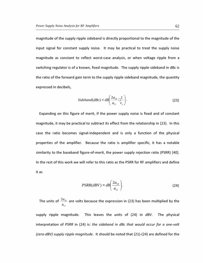
* Change in PSRR when effect of parameter is included (i.e. gmo11 is shown to reduce PSRR from infinite to the edge of the shaded region indicated in the legend).
# + 3 & ( (
01 01* '
+ , ! 0**0<611* +,!'* ' )) 3*!01, 3+ && ,
(*-0

Power Supply Noise Analysis for RF Amplifiers 86
13+
&*())&
( * # 3' )) ,
& * 7+&'
, -'* # +3')) + ( , +
*,+&*,'' .<7&*#!
*
& *2+3' , ,*0<:1!0881',,,
?*
# 2 8E' ? & + .
,+*/
! .' )) ,*
+ ' &
&?*&
'' *;&',&*

Power Supply Noise Analysis for RF Amplifiers 87
#++)2+
* & +
.!+
)2*)&,+++6!
* + 9
& :"75 *8975 + + + 6!<* "!
?+,&,&
&3 +*
' IC J' , & !
+, 3 . !3
* & )2 &
& + -' , !! 0;1
'&&(01
+*

88
Chapter 5 Optimum Operating Strategies for Hybrid Voltage Regulators
,
Figure 49. Model for parallel hybrid switching-linear regulator
#<'&&
&+&(*
&,,'++

Optimum Operating Strategies for Hybrid Voltage Regulators 89
0#1.+*7,&'
+ 2 8 ' &
* . &, ,
+&*
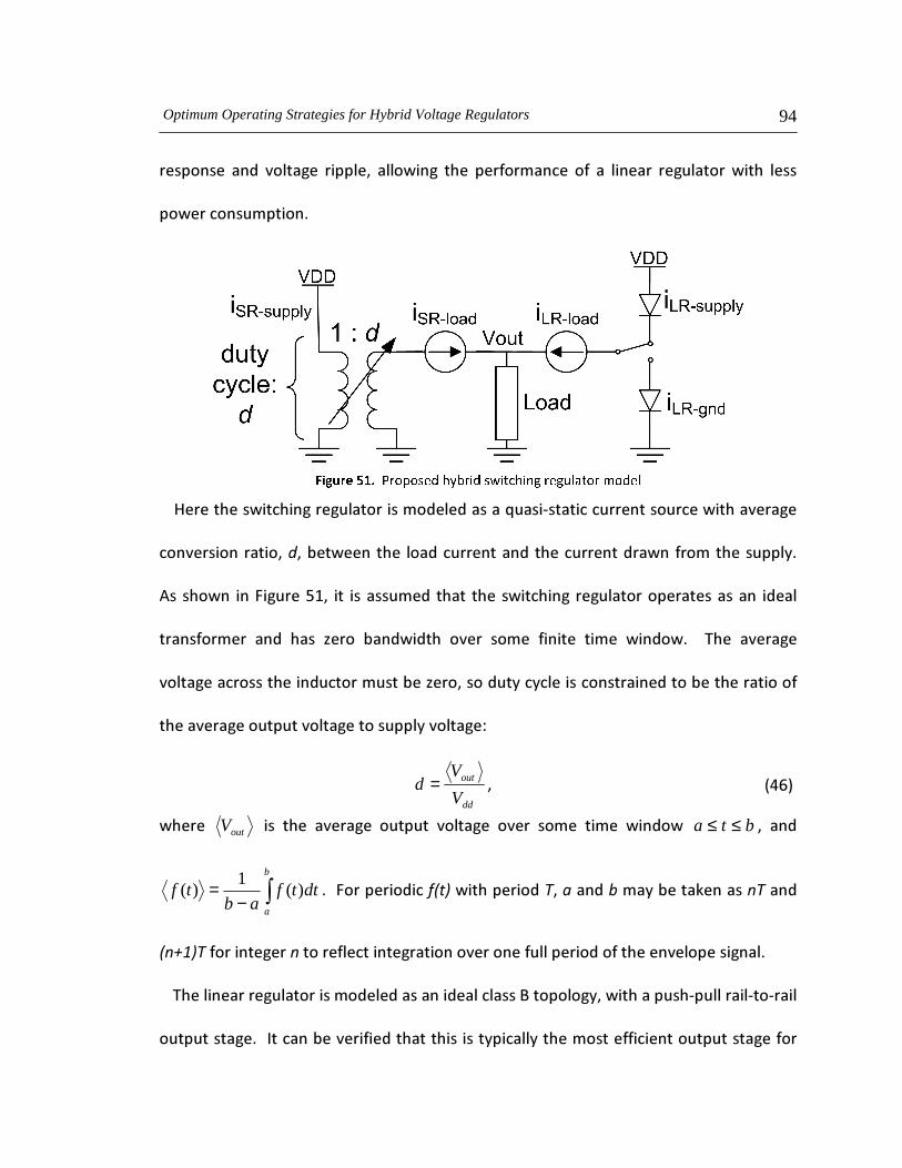
28 +,&<**<*
&+'#&*
+'
'&*#
+Figure 49*/,
' + &
IEE!E:J*
, & & ,
,&&&*
/,' ! &+&
*,(&&
+ * 7+&' +
&',*
& & + &
&0";&1*
,+ A + ! &' , 3
+ 3' +* #
Optimum Operating Strategies for Hybrid Voltage Regulators 90
, ' , + *
,+,&&
' + + +' , +
*
/ , ' !,+ &
& + I6<' =' =8J' +
+ & &
I ' 6J*,,',
&,,IC6'C' J'
! I <' 8J* / ' +
,+ ( , & +
0! 1 '+ & , + &
. I =! EJ* 7+&' ' &
,+( ! & +
+ 3 I<C' 8=' 8E' =J* / ' ,
, ' ,+'
IC6'CJ*
2 + 2 8 ' & & ,
, + ,(*
+ , &
Optimum Operating Strategies for Hybrid Voltage Regulators 91
& * D ,(
&*,+
, !,+ +,
"75 I=' =8J* /
+,+',
+ ! & I <' 8J'
+ & * ' &
'
+*/+('+
& 5 +
0!1'IC6J''I J*+
&!5,++*#
,+ +
ICJ*
Overview ,.&
)2 + * . +( IC6' C' ! 8J +
,* /+
+ 3! *
&&3

Optimum Operating Strategies for Hybrid Voltage Regulators 92
,++*+(
+ & " * / +
5,+3!*/
',++3!'+
,53*
0 1 2 30
5
10
15
Sig
na
l A (
V)
0 1 2 30
5
10
15
Sig
na
l B (
V)
time (s)0 5 10 15 20 25
-100
-80
-60
-40
-20
0
20
frequency (Hz)
Po
wer
Sp
ect
rum
(dB
/Hz)
PAPR=5.2 dB
PAPR=10.1 dB
Figure 50. Two different time-domain envelope signals that share the same power spectrum: one with
peak-average power ratio (PAPR) of 10.1dB, and another with PAPR or 5.2dB.
, 3
ICJ*23!,
& + * # . +
Figure 50* 7'+&+&+
*(!&+0#)16*6'
+#)=** / 5
,*,!

Optimum Operating Strategies for Hybrid Voltage Regulators 93
+ 5,++
!*
/'+&.+
&' & &'
& * 5 ,
* / +
' +
&++*&IC6'C' J'
,+ , &&
&,+* /'++.
'3!+,
*&+
,3!,&+
/!:= "#/ *66A*
& ' +
A , 5
+3I8='==J*D''&
!,+ ' , & + + '
+ & * ,
Optimum Operating Strategies for Hybrid Voltage Regulators 94
& ' + +
+*
7+3!+&
&'',+ +*
#+ 2=6' +
5 ,+ & ++* &
&,5',
&&&
dd
out
V
Vd = ' 08C1
+ outV & & & ++ bta ≤≤ '
∫−=
b
a
dttfab
tf )(1
)( *2+#',(#
$#&&*
'+!!!
*/,&

Optimum Operating Strategies for Hybrid Voltage Regulators 95
I8J* !'
'+ (* 2
+&'+,
+ *
,+,(
*+ &*
+ + ,+!<C
* ,&,&
'
S
L
P
P=η ' 08E1
+ LP &+ SP &+
*#2=6'&+
+
[ ]diiVP SRLRDDS ⋅+⋅= ' 08 1+ LRi ' SRi +&'
' DDV , &* &
&& ' LRi SRi * 2
&+&'#"+!)2'.
08E1 08 1 , & . ,
& , &* / , +

Optimum Operating Strategies for Hybrid Voltage Regulators 96
08 1 ' .
+*#'
=*8' ,
&* ) + , &*
&',
5* . !#" +!
. , 3!
,* 2 + ' "#' %"
*66'!
& +&* 7+&' LRi SRi , '
, , ' + , =*C*
' . & +&
+ ' & 5
&,*
& . )2 +
, .* 2
)2 ' & & +& ,
+

Optimum Operating Strategies for Hybrid Voltage Regulators 97
)cos()( wtvvtv aDCo ⋅+= '
)cos()( wtiiti aDCo ⋅+= *08:1
7'&&'&' &*/08:1'+(' , & &
,*
0
0.2
0.4
0.6
0.8
1
0 2 4 6 8angle (radians)
En
velo
pe
volta
ge
(no
rmal
ized
)
Sinusoidal AM Two-Tone
2 = + 5 & & !#"
+! * / !#"
DCa vv = * & + & '
'
.2
)()(1
0
aaDCDC
T
ooL
ivivdttitv
TP
⋅+⋅=⋅= ∫ 0=1
&.&++'08 1'
& LRi & , SRi

Optimum Operating Strategies for Hybrid Voltage Regulators 98
& ' ' T'
*
0
0.2
0.4
0.6
0.8
1
curr
ent
(A)
-Φ +Φ
iSR
iDC
<iLR>2Φ
iLoad
2=<+ +& ,* /
+ '
. 6 * + ! ' & * 7+&' .
+2=<'+
TU6 * &,+*2+&08:1'Φ ,&
−
=Φ −
a
DCSR
i
ii1cos * 0=61 0=61' & ,+

Optimum Operating Strategies for Hybrid Voltage Regulators 99
( )
[ ].cossin
)cos(2
1
ΦΦ−Φ=
−⋅+= ∫ΦΦ−
π
φφπ
a
SRaDCLR
i
diiii 0=1
7'&
+*&'
2=6',+&+&
08C1' 08 1' 0=1' + +
,&'*/,0=1
+ + * #& #"
&+
[ ]ΦΦ−Φ+⋅
⋅+⋅
=cossin
2
π
ηa
ddDCSR
aaDCDC
iVvi
iviv
* 0=<1
/ 0=<1' & + &
+&' &' ' T' *
, 0=61 0=<1'& .
,+' SRi *%',5
, + & . &
* 0=SRdi
d η ',
⋅+=
dd
DCaDCSR V
viii πcos* ' 0=81

Optimum Operating Strategies for Hybrid Voltage Regulators 100
+ *SRi 3! + * .
&' *η '& *SRi .
( )*
*
sin
2
Φ+⋅
⋅+⋅
=
π
ηa
ddDCDC
aaDCDC
iViv
iviv
' 0==1
+ *Φ ',+
dd
DC
V
vπ=Φ* * 0=C1# 0=81' , +
3 ',
&+&*
IC6' J' +
+ *
+! ' . .
, ,* 2
)2 + 3' 2w 1w ' , 3
' ' & !+& + ( &
va×2 'ICJ'
−⋅= t
wwvv aenv 2
cos2 12 * 0=E1/'+
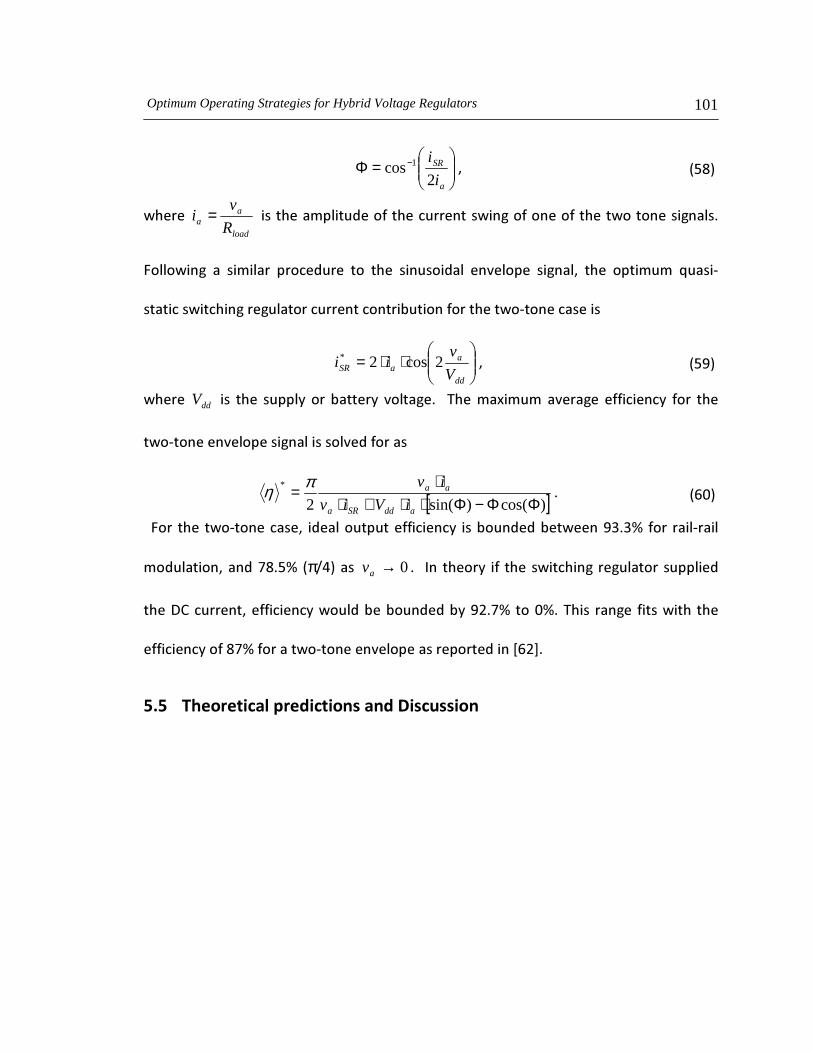
Optimum Operating Strategies for Hybrid Voltage Regulators 101
=Φ −
a
SR
i
i
2cos 1 ' 0= 1
+load
aa R
vi = ++*
2+ & ' 3!
+,+!
⋅⋅=dd
aaSR V
vii 2cos2* ' 0=:1
+ ddV , &* .&
+!&&
[ ])cos()sin(2*
ΦΦ−Φ⋅⋅+⋅⋅
=addSRa
aa
iViv
ivπη * 0C12 +!' ,,+:<*<> !
'E *=>0πA81 0→av * / +
'+,,,:*E>>* +
E>+!&ICJ*

Optimum Operating Strategies for Hybrid Voltage Regulators 102
00.10.20.30.40.50.60.70.80.9
1
0 0.1 0.2 0.3 0.4 0.5Modulation Amplitude, Normalized (V)
Effi
cien
cySin-AM isr=isr*Sin-AM isr=idc2-tone isr=isr*2-tone isr=idc
00.10.20.30.40.50.60.70.80.9
1
0.0 5.0 10.0 15.0 20.0 25.0Average Output Power (dBm)
Effi
cien
cy
isr = idcisr = isr*
! "#$%&'
2 =8 + & !#" +!
*&
5 6?' + !! +
5*2#"'
DCa vv = *+!+3+
' ' 0=E1* / + ,

Optimum Operating Strategies for Hybrid Voltage Regulators 103
' & > *
7+&'+' *SRi '&0=81
0=:1'&,('
+0==10C1*'
+& &*/&'
,.,
• #+&'+ */
' 0180 !&*&2=8&*
• #+++ '
'!#"' aDCSRia
iii +=→0
lim */+'
!+
0180 *#&'+!#'++*
+ 2 =8 ,& +
* 2 == + & + &+&
/!:= !& ! 0 "#1* /
&+& +,-
3 * ' 2 ==' & +

Optimum Operating Strategies for Hybrid Voltage Regulators 104
,& * ; *SRi &
* "# +&
&2=8*,!#"'+! "#+&
&(!!&+0#)1*#)
3 ,+
. & & & & & I6' <' J*
9'#)&++*,
& & & &
*
&,++ *SRSR ii = '
+ DCSR ii = ,++
,(* /+ DCSR ii = '&5
+ & * 7+&' ' ,
+ &'min
η * 2
2 =8'min
η ,+ E! >* & "# '
minη HC >*'+.+,('+,
& & 3, #' , , &* F. + + & + ,( I :J* / ' !,+ + & + ,+ ! ,

Optimum Operating Strategies for Hybrid Voltage Regulators 105
& I88J* + + &+ ,* (###)! !
*SRi ( )*cosΦ⋅+ aDC ii ( )*cos2 Φ⋅⋅ ai
*Φ dd
DC
V
vπ dd
a
V
v2
*η ( )*sin
2
Φ+⋅
⋅+⋅
πa
ddDCDC
aaDCDC
iViv
iviv ( )*sin2 Φdd
a
V
vπ max
η %7.9142
3 =+ππ %3.93
)1sin(4=
⋅π
minη %75
4
3 = %5.784
=π DCa vv =
!"## $
%
% *SRi % &
$'(%
%

Optimum Operating Strategies for Hybrid Voltage Regulators 106
% *SRi %)'(*
*SRSR ii =
% DCSR ii =
% +
)''* ),!*
% &
-' ... !"##

Optimum Operating Strategies for Hybrid Voltage Regulators 107
)/0#0#* 1
)&& !'!2 ''!*
%
% 3
&
4''%'-%-!5
% )''* ),!*%
%
% %)(,*%
/
%,
$',% 6
7 2 #!!&2
/
"!89 % &-' !"##:/7

Optimum Operating Strategies for Hybrid Voltage Regulators 108
6
%
; Ω10
+
0.3
0.4
0.5
0.6
0.7
0.8
0.9
0 50 100 150 200switching regulator current (ma)
Eff
icie
ncy
measuredtheorymeasuredtheory
Vdd=3V; Vo=1+1*sin(wt)
Vo=0.5+0.5*sin(wt)
Supply Voltage= 2V; Signal=va+vaSin(wt)
00.10.20.30.40.50.60.70.80.9
1
0 0.2 0.4 0.6 0.8 1Normalized Voltage Amplitude (V)
Eff
icie
ncy
theorytheorymeasuredmeasured
isr=isr*
isr=idc
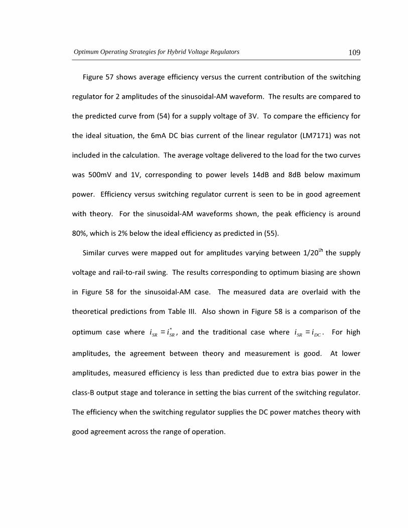
Optimum Operating Strategies for Hybrid Voltage Regulators 109
$'0
"
)'(*<=
% , )/0#0#*
'!!= #=% #( 1 1
.
$ % +
!>%"> )''*
& #2"!
$ '
$'
*SRSR ii = % DCSR ii = $
%
%
1

Optimum Operating Strategies for Hybrid Voltage Regulators 110
Supply Voltage= 2V; Signal=2*va*abs(Sin(wt/2))
00.10.20.30.40.50.60.70.80.9
1
0 0.2 0.4 0.6 0.8 1Normalized Voltage Amplitude (V)
Eff
icie
ncy
isr=isr*isr=idcisr=isr*isr=idc
isr=isr*
isr=idc
!
0.2
0.3
0.4
0.5
0.6
0.7
0.8
0.9
-5 0 5 10 15 20 25Average Output Power (dBm)
Eff
icie
ncy
isr=isr*isr=idcisr=isr*isr=idc
CDMA
802.11a
"#$%&'() **+,-$ '-
9 '( 9
%
-!,> -<<>

Optimum Operating Strategies for Hybrid Voltage Regulators 111
$,! ... !"##
)&*
/ 7'("#%
$', #!Ω
6
"! 1 !"## '(12%
#' 1+);;?*
!"## );;?@#! 1*
;;? !"##
% $ ,!
$''
<<=
#:

Optimum Operating Strategies for Hybrid Voltage Regulators 112
0
0.5
1
1.5
2
2.5
-5.00 0.00 5.00 10.00 15.00 20.00 25.00Average Output Power (dBm)
isr*
/idc
CDMAWLANSinAM
. /0 DCSR ii /* 1 $,#
DCSR ii /*
&
:/7
;;? %
*SRi DCi⋅2 % )'(*
& *SRi
DCi DCSR ii /*
?% %*SRi 9% SRi ++
+ %

Optimum Operating Strategies for Hybrid Voltage Regulators 113
*SRi $%
%63
% $ '-,#
% *SRi %
%
%
% *SRi
8% + *SRi
+ % 4 !5
9 $'-,#%
Figure 62. Hybrid regulator model including output capacitance

Optimum Operating Strategies for Hybrid Voltage Regulators 114
%
Figure 62
%
6 %
% RC=τ %+3
%
6
)cos()( twvvtv aaDCo ⋅+= % ),#* DCv % av %
aw 3
[ ]
+⋅⋅+=R
Cjwtwvvti aaaDCo
1)cos()( % ),"*
R
Cjwa
1+ is the admittance of the load network at the frequency of the AM tone.

Optimum Operating Strategies for Hybrid Voltage Regulators 115
The current supplied to the load by the linear regulator, following the development of
section 5.4 follows as
[ ] )(1
)cos()( tiR
Cjwtwvvti SRaaaDCLR −
+⋅⋅+= % ),<*
⋅+
−=Φ −
aaa
DCSR
VCjwi
ii1cos ),(*
),(*% %3
3%
+
−=Φ −
RCjwi
ii
aa
DCSR
1
1cos 1 ),'*
( ) φφπ
dRCjwViii aaSRDCLR ∫Φ
Φ−
+⋅+−= /1)cos(2
1 ),,*
),,*
[ ].cossin~
ΦΦ−Φ=πa
LR
ii %
RCjwii aaa += 1~
),0*
%
),0* A 9

Optimum Operating Strategies for Hybrid Voltage Regulators 116
% %
0=SRdi
d η
DD
DC
V
Vπ=Φ* % ), *
** cos~ Φ+= aDCSR iii % ),-*
*
*
sin~
2
Φ+
+=
π
ηa
DDDCDC
aaDCDC
iViV
iViV
)0!*
8%), *)0!*)'(*)',*%
3
3 3
8%3
%
00.10.20.30.40.50.60.70.80.9
1
0 0.1 0.2 0.3 0.4 0.5Normalized time constant (wRC)
Effi
cien
cy
Vo=0.5+0.5Cos(wt) --Calc
Vo=0.5+0.5Cos(wt) --Sim
Vo=0.25+0.25Cos(wt) --Calc
Vo=0.25+0.25Cos(wt) --Sim

Optimum Operating Strategies for Hybrid Voltage Regulators 117
Figure 63. Hybrid regulator with load capacitance: efficiency versus normalized time constant (simulation vs theory)
Figure 63 ?
% Figure 629 3
3
3 )0!*
& 8%
), *)0!*
Figure 63 3
#2#!%
8% 3
3% 3B
3%
3
$
$%
%3%

Optimum Operating Strategies for Hybrid Voltage Regulators 118
Parallel hybrid voltage regulators are highly practical for dynamic supply transmitter
applications. These topologies can provide fast dynamic regulation with low noise and
high efficiency. If the operating conditions are carefully considered, power efficiency
can be comparable to a pure switching regulator solution. The key is to consider the
time-domain operation of the switching and linear regulator portions as many waveforms
can have the same power spectrum. In many cases, the switching regulator should supply
more than the average load current, with the linear regulator sinking more current to
ground in a push-pull output stage. There are many conceivable circuit architectures that
could optimize the bias conditions of the hybrid regulator through online sensing and
slow adaptive feedback. A final practical consideration includes the dynamics of the load
network. From an efficiency perspective, it is best to have any poles at the output be
substantially higher frequency than the modulation signal to avoid reactive losses. This
implies that the linear regulator may be best optimized with internal compensation rather
than using a dominant pole at the output.

119
Chapter 6 Direct Digital Modulation: A New Approach to Polar Systems
Figure 64. Conventional cellular phone block diagram: digital application processor, DSP, Audio, Power
management; Radio is still largely analog
Figure 65. Proposed digital polar architecture
& Figure 64%
% &;%%
8%
% %
'! 4#!5

Direct Digital Modulation: A New Approach to Polar Systems 120
C& :
$
-!C& 1
"#D.? <12
Figure 65
% + ?$
%
?$
% 39 #
?$
3
Σ∆ 4-#5 . Σ∆ ?$
E4-"5 :4-<5
+ E 4-(5 1 4-'5 C
4-,- 5
+
Figure 65 ?
% Σ∆
1
%
Direct Digital Modulation: A New Approach to Polar Systems 121
3
':6+;
%
.=>"!+
6.1 Transmitter concepts revisited
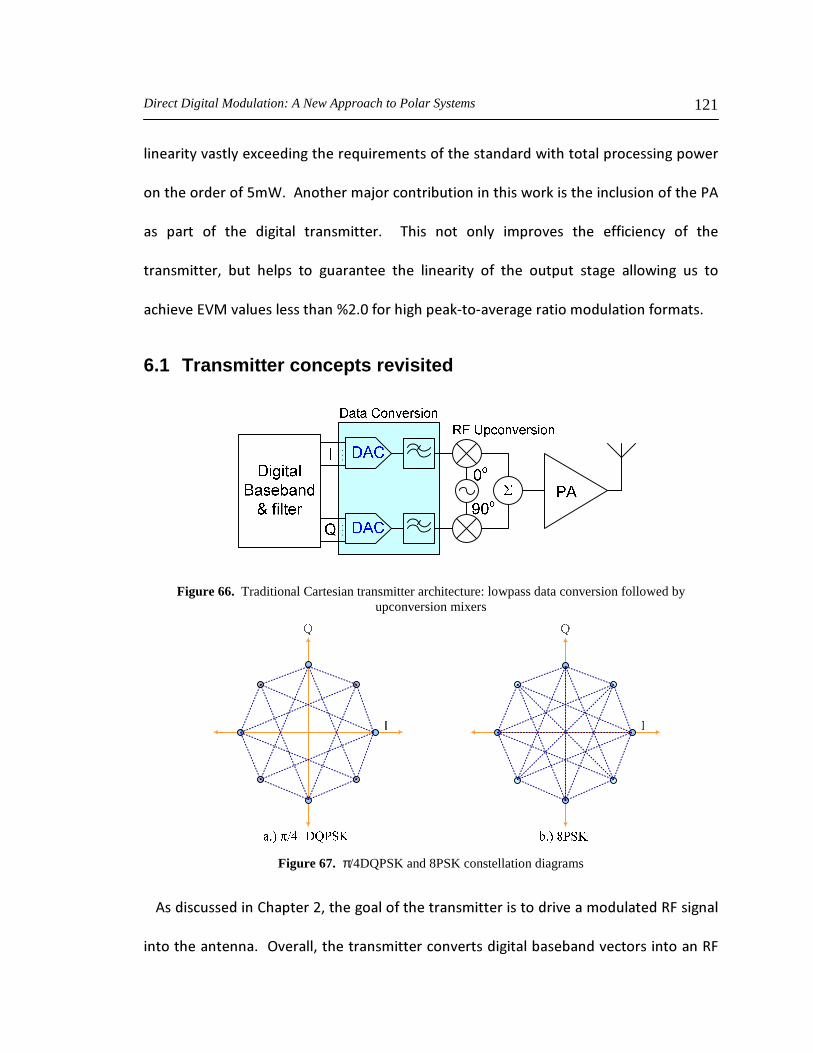
Figure 66. Traditional Cartesian transmitter architecture: lowpass data conversion followed by upconversion mixers
Figure 67. π/4DQPSK and 8PSK constellation diagrams
"% ?$
C% ?$

Direct Digital Modulation: A New Approach to Polar Systems 122
1 %
% + + % ?$
?$ 6 3
).=*% "#" &
+ 6 );?*
6 π2(F;&G ;&G )
* Figure 67
1"#D.?
"12 <12 4-5
3
%
Figure 66% ?$
?$ 6 8%
3H 3 ?$ ;
1 ;
%
/C%%

Direct Digital Modulation: A New Approach to Polar Systems 123
?$ :
%
% 39
6.2 Data conversion principles
000 001 010 011 100 101 110 11100.1250.2500.3750.5000.6250.7500.8751.00FS
out
V
V
Binary Input 1000
VFS∆=LSBV
Figure 68. Input-output transfer characteristics for a 3-bit D-A converter
3 Figure 68
<8% 9.
N
VFS % FSV
3

Direct Digital Modulation: A New Approach to Polar Systems 124
)/&1* LSBFS VV − $
4--5%% FSV % ( )N
NFSout bbbVV −−− +++= 222 22
11 L )0#*
.3)0#*
39
% 3
39
3
6.2.1 Quantization Noise
000 001 010 011 100 101 110 11100.1250.2500.3750.5000.6250.7500.8751.00FS
out
V
V
1000Quantization ErrorAnalog Input +½
-½
Figure 69. Comparison of continuous and quantized signal levels showing error between ±½ LSB

Direct Digital Modulation: A New Approach to Polar Systems 125
: 39%
Figure 69
39 %
399 39
3 $ % 39
∆± 21 % ∆ 399
/&1:%
12
22
2
22 ∆=
∆= ∫
∆+
∆−
dee
e )0"*
.3 )0"*
4#!!5 % 2e %
73
%
39
6.2.2 Discrete-time sampling
Figure 70. Frequency-domain representation of discrete-time sampling process

Direct Digital Modulation: A New Approach to Polar Systems 126
: %
6
73 73&
%
% Bf S 2< %
%
&%4#!#5%
3
&I
( )
∫∫
−
∞
∞−
=
=
B
B
iwt
iwt
dwewF
dwewFtf
π
ππ
π2
2
,)(2
1
)(2
1
)0<*
3 )$ *
B
nt
2= %
∫−
=
B
B
B
niw
dwewFB
nf
π
ππ
2
2
2 ,)(2
1
2 )0(*
B
nf
2 ( )tf )0(*
$ ( )wF & ( )wF

Direct Digital Modulation: A New Approach to Polar Systems 127
9 ( )tf % ( )tf
B
nf
28%
%
( ) ( )( )∑∞
−∞= −−=
nn nBt
nBtxtf
ππππ
2
2sin % )0'*
6.2.3 Practical sampling and reconstruction
fT
fTefH fTi
πππ )sin(
)( −=)( fH
Figure 71. Time- and frequency-domain characteristics: zero order hold (ZOH) reconstruction
: )0'*
%
; 9 )JC8*
& Figure 71%
%8%JC8
% 3%

Direct Digital Modulation: A New Approach to Polar Systems 128
Figure 71JC8
%3
3 3 $ % JC8
3
6.2.4 Sampling with non-bandlimited signals, and relationship with quantization noise
Figure 72. Signal and noise before and after sampling
%2Sf
+ 3
733 +
73 3
Figure 72
733 %
+3
Figure 72 I
% 3

Direct Digital Modulation: A New Approach to Polar Systems 129
%3
3%
3 8 3 H
H
%
39
Figure 73. Quantization noise spectral density: a.) Nyquist-rate sampling, b.) Oversampling
,"#%39
73
% &
Figure 73% 73 %
39 % % %
239 %

Direct Digital Modulation: A New Approach to Polar Systems 130
%
39
6.3 Oversampled Data Converters C
% 39
% 2
% 39
39 +
%39
7
2
Figure 74. Signal and quantization noise with noise shaping

Direct Digital Modulation: A New Approach to Polar Systems 131
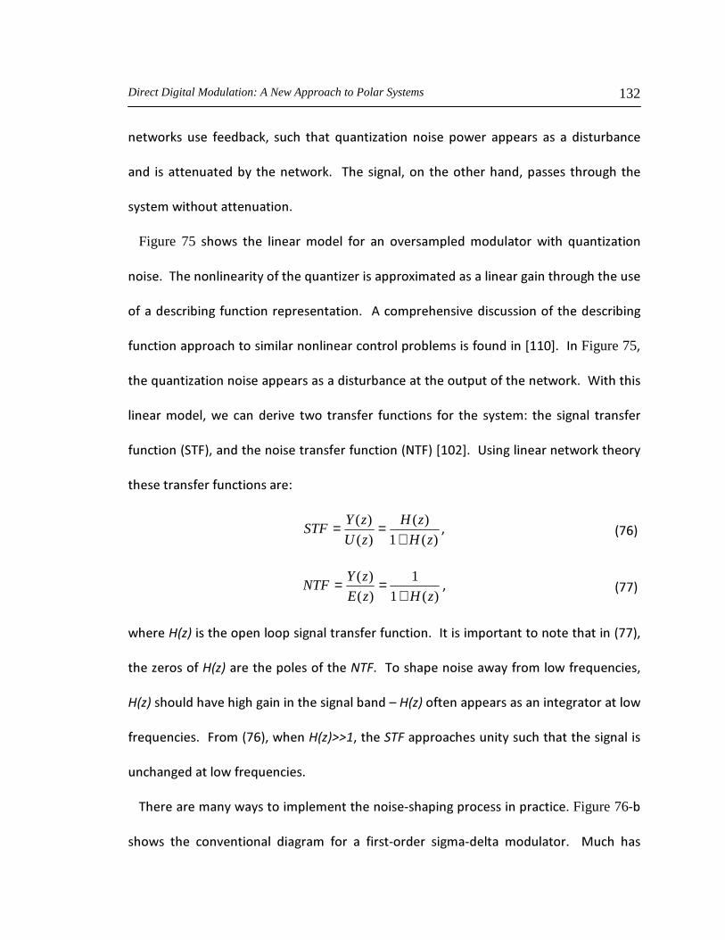
Figure 75. Linear model of the noise-shaping process: quantization noise appears as a disturbance
Quantizeru[n] y[n]
e[n] +-G(z)-1x[n] Quantizeru[n] y[n]+- z-1++
b.) Sigma-delta modulatora.) Error-feedback noise shaping Figure 76. Noise-shaping data conversion blocks: a.) Error-feedback structure, b.) first-order sigma-delta
modulator
6.3.1 Noise Shaping + 39
39 %
Figure 68% %
H 3 7
Direct Digital Modulation: A New Approach to Polar Systems 132
+ +% 39
+ % %
Figure 75 39
39
4##!5Figure 75%
39 +:
% I
)&$*% )7$*4#!"5A+
I
)(1
)(
)(
)(
zH
zH
zU
zYSTF
+== % )0,*
)(1
1
)(
)(
zHzE
zYNTF
+== % )00*
)00*%
93%
H
3$)0,*%%
3
Figure 76

Direct Digital Modulation: A New Approach to Polar Systems 133
A
4#!!%#!"%#!<5
4#!"5
+ Figure 76%
39 ) 39 *
: %
: %
1
1
1)( −
−
−=
z
zzH
( )11 −−= zNTF % )0 *
1−= zSTF )0-*
$ )0 * )0-*% 39
3% 3
Figure 74%
3
% 2

Direct Digital Modulation: A New Approach to Polar Systems 134
)log(3017.576.102.6 OSRNSNR +−+= % ) !*
39
.3) !* 2
- 1)#'*
39 &7?
+ % Figure 76 *%
39 6+
4#!(58% 1)( −zG
1)(
)()( ==
zU
zYzSTF %
% )()(
)()( zG
zE
zYzNTF == $?
$ +
[ ] 11 1)1(1)( −− =−−=− zzzG %6
+ 4--5 4#!"5

Direct Digital Modulation: A New Approach to Polar Systems 135
6.3.2 RF (Narrowband) Digital-Analog Conversion (DAC)
FS
out
V
V
Figure 77. RF DAC: quantization of RF carrier amplitude
Figure 78. Frequency-domain RF DAC with sampling images
?$
3
$ Figure 77%
3 %
%
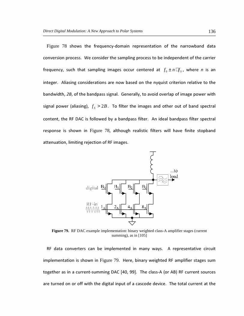
Direct Digital Modulation: A New Approach to Polar Systems 136
Figure 78 3
:
3% Sfnf ⋅±0 %
3
% % K%
)*% Bf S 2>
%?$
Figure 78%
%6?$
Figure 79. RF DAC example implementation: binary weighted class-A amplifier stages (current
summing), as in [105]
?$
Figure 79 8% ?$
4(!%--5)1*?$

Direct Digital Modulation: A New Approach to Polar Systems 137
C&; 4#!'5
C$", 1.=
Figure 80. Bandpass Σ∆ modulator with center frequency at 4
sf
C %
4-#% -"% - 5 Figure 80
Σ∆ 8% Σ∆
2
1
1)( −
−
+=
z
zzH % ) #*
jz ±= 4
sf effectively shaping
noise away from the 4
sf frequency range. The oversampling ratio in this case is
B
f s
2
where 2B is the bandwidth of the narrowband signal. For traditional bandpass Σ∆
%%% 3%

Direct Digital Modulation: A New Approach to Polar Systems 138
6.4 Direct-digital modulation for RF transmitters
Figure 81. Direct digital modulation: transmitter operating as a D-A converter
: ,# ?$
% + +
?$
.=
+Figure 81?$
I %
3 ?$
,<" ?$ %
%
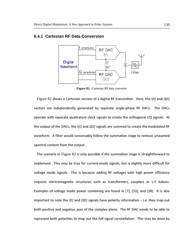
Direct Digital Modulation: A New Approach to Polar Systems 139
6.4.1 Cartesian RF Data Conversion
Figure 82. Cartesian RF data converter
Figure 82 ?$8%! "
?$
3 +!#"
%! " ?$
Figure 82
%
?$
3 % /
. 405%4<<5% 4< 5
! "H
?$

Direct Digital Modulation: A New Approach to Polar Systems 140
6 # ! and 2700 clock signals to the appropriate DAC, or phase-shifting
(inverting) the LO signal inside the DAC.
-!!89?$ 4- 5%!$"
) Figure 82* 4- 5% ?$
Figure 79 :
% &7?'< 1
6.4.2 Polar RF Data Conversion
Figure 83. Polar RF data conversion: RF amplitude DAC with phase-modulated clock signal
; %
%
?$ ;6 ?$
?$+Figure 83 ?$
&
% 6

Direct Digital Modulation: A New Approach to Polar Systems 141
,<"
%
; .=
3 ?$ +
"<#?$+
% ;//4",5 1
.=
+3: 4" 5%
+
4-'% #!'% #!,5 + 4#!'5
; Figure 79 39 ?$
?$, 39
0"> );.* #,K89 3 %
Figure 12% ?$;C", 1
.= "!89 C$ #<, 1 $
,'
6.4.3 Issues with spectral images

Direct Digital Modulation: A New Approach to Polar Systems 142
&
+&Figure 78%
sfnf ⋅±0 % ;
) *+ 9
Figure 71 8% %
3
%
4#!'5+
(
sff ±0 % 0f 3 sf
sff ±0 % sfOSR ⋅ %
Figure 84. Upsampling to reduce spectral images, process in Pozsgay [106]
&Figure 84%4#!,5

Direct Digital Modulation: A New Approach to Polar Systems 143
3:$2: "K2<K &#"
!$"% "!89% #,!89 $?
+ !$"%
20f %#"K89
20f %
6
?$ ) Figure 79*
+", 1"(>.=
+ 3
"'(:", 1)# :*

Direct Digital Modulation: A New Approach to Polar Systems 144
6.5 A 2.4GHz RF Polar Transmitter for Bluetooth 2.1+EDR
Polar Digital BasebandAmplitude Path
Phase PathDigital Phase ControlRF DAC
Class-D1-bit PARF Pulse-Density Modulator(@ 2.4GHz)Baseband Modulator(@100MHz) A Matching+BPF2 V
RFclk(Φ)BBclk
Figure 85. Digital polar modulation architecture
6.5.1 Introduction #% %
C& % 3 +
+
1"#D.?
?$
"(K89+
4-(- 5% ?$ ; %
; ?$ %
D"! 1 6 + 3

Direct Digital Modulation: A New Approach to Polar Systems 145
) 1*
9 3 %
+ " : <!>
1
&Figure 85% ;
; 7C& ;C& :
;C& (!K89 -! %
C& 8
3 )F* %
+
3 : %
F"!<!+4#!05
;
?$ + ).*
40% 0 5 : %
%
+);;?*/
%
1 %
; % ;
4"-5

Direct Digital Modulation: A New Approach to Polar Systems 146
6.5.2 Architecture
a.) Polar system with PWM supply regulation
RF Φ
Reactive BPF
Phase Path
Power Amplifier
Pulse-Density-Modulation
Amplitude Path
b.) Polar system with PDM in the PA
Figure 86. Candidate polar architectures
Figure 85
& Figure 86% ;:
% Figure 86
;
);:* & ;:

Direct Digital Modulation: A New Approach to Polar Systems 147
Figure 86% );*
?$3
%
;
;:
<""% ;:
;
3 ; %
;: ?$ %
;Figure 86%
%;
%
C
%
3&

Direct Digital Modulation: A New Approach to Polar Systems 148
Figure 87. Time and frequency domain examples for full- and half-amplitude modulation
&$ '%
%; '!>
+ F
3?$ ;
?$
# 3 ∆Σ
39 ∆Σ
,'<%
?$ 3 +
?$ ;

Direct Digital Modulation: A New Approach to Polar Systems 149
3
& $ 0%
8
4#! 5%
) * 3
$Figure 87% 3 12=loadedQ
'!> ), 1 +*% -'>
4#! 5
+$ ;%
/+ ;
%

Direct Digital Modulation: A New Approach to Polar Systems 150
6.5.3 Pulse-density modulator (PDM)
Figure 88. Pulse-density modulator block
; + Figure 88 % %
39 9
);*+∆Σ+#
∆Σ #!!89 +
9 "(K89 )&'
* ;
?C
3 #! 39
3 3 9
Direct Digital Modulation: A New Approach to Polar Systems 151
++
9 %
%
;+;
?$+?$+ ;
#
;
$% %3L9M LM
% # % 3 Figure 87;
#2- #(%",,89"(K89
∆Σ
6.5.4 Polarity Bit

Direct Digital Modulation: A New Approach to Polar Systems 152
Figure 89. 1-Bit polarity feedforward to reduce power from rapid phase transitions
Figure 90. Constellation diagram for 8DPSK with feedforward phase transition: 4
5
4
ππ →

Direct Digital Modulation: A New Approach to Polar Systems 153
Figure 91. Polarity bit significantly reduces high frequency power in the RF clock signal waveform by
smoothing phase transitions near origin
"<"%
6%
F 9
8% % %
3 Figure 90 ;&G
: ;&G%6%
# !

Direct Digital Modulation: A New Approach to Polar Systems 154
%
Figure 89
# :
% + % # ! ! # !
(3
+)!%-!%# !% "0!*%
3
: % 9
1
% ) *
A
9 + %
Figure 91 3
F Figure 91LMLFM

Direct Digital Modulation: A New Approach to Polar Systems 155
%F # ! 3 % 3
F #!89%<! 1
F 3
Figure 92. Effect of polarity on amplitude quantization - ∆Σ process remains linear near zero
:
% &
Figure 91% 3
8% ?%
3
∆Σ
∆Σ Process remains linear
Digital-in
RF-out

Direct Digital Modulation: A New Approach to Polar Systems 156
:% ∆Σ 9 %
9 6
1 9%
9
9)+*
6.5.5 ∆∆∆∆ΣΣΣΣ Noise-shaping process +% ∆Σ
39 #!
#" ?C #!
39 ( ; + :
+ 3#!!89%+
3'!89
22 QIA +=
Figure 93. Error-feedback digital ∆Σ modulator

Direct Digital Modulation: A New Approach to Polar Systems 157
∆Σ +%
$-< ,<% +39
)()(
)()( zG
zE
zYzNTF == %))*)$)+)$,*%
1)( −zG 4--5
$? Figure 93% %
( )211)( −−= zzG %9989
0 10 20 30 40 50-90
-70
-50
-30
FREQUENCY (MHz)
PO
WE
R (
dBm
)
Figure 94. Example baseband 3rd order ∆Σ modulator spectrum with a notch at ±12MHz,
123 5.25.2)( −−− −+−= zzzzG

Direct Digital Modulation: A New Approach to Polar Systems 158
Figure 95. ∆Σ Modulator: 1st, 2nd, 3rd order comparison, all zeros at 2.4GHz
$-( $-' + $
-( 9
9'89 %
#"89 7
39+3
A% +
) * 39 Sff ±0 % 0f
3 Sf 3∆Σ %
+ +%
+
Figure 95 3
<

Direct Digital Modulation: A New Approach to Polar Systems 159
3%+
+ %
6.5.6 Class-D PA
Figure 96. Complementary class D PA schematic
&
.
$ 3
4<(5 8%
+
C&
+ %
Direct Digital Modulation: A New Approach to Polar Systems 160
&Figure 96%;C&
% 3%
+ +
+
+ . $
. + % $
3+
%
4<(5%
)$C*
I
DC
pkV V
VF ≡ % ) "*
DC
rmsI I
IF ≡ . ) <*
) "* ) <*% + % ! !?&
8
8 ?&
+

Direct Digital Modulation: A New Approach to Polar Systems 161
Table IV. COMPARISON: FV-FI FIGURE OF MERIT FOR VARIOUS AMPLIFIER CLASSES
(DATA FOR CLASS E, F-1, F2,3,4,5 FROM [34])
Amplifier Class FV FI
E 3.56 1.54F-1 3.14 1.41
E/F2,3,4,5 3.20 1.45D 2.00 1.57
Table IV C
% .
+
& %
=
+ +
%
7C& 8%
% (!K894"5
3 4#5

Direct Digital Modulation: A New Approach to Polar Systems 162
$ %
+$.$%
+
=
+
; .
$ ;
6.5.7 CMOS Class D PA Implementation
Figure 97. Schematic representation of class-D power amplifier with cascode output stage

Direct Digital Modulation: A New Approach to Polar Systems 163
Figure 98. Current recycling scheme: excess current from PMOS drive stage used by digital processing
Figure 99. Class-D PA output stage NMOS layout: gate and cascode share diffusion region to reduce
junction capacitance
Figure 97 C& ;
% %
source drain source drain
G C C G G C
current
5µm

Direct Digital Modulation: A New Approach to Polar Systems 164
+ 4#!-5;
%- .% %/+&-.
#!=
& Figure 98% /+&
;C& 7C&
;C& ;C&
97C& #!=
+% 3 /+&
#!!$
3 &
/+&
9 #!!: )"! 1*
"(K89
8 %
& Figure 99%
6
'N9

Direct Digital Modulation: A New Approach to Polar Systems 165
Figure 100. Level shift and deadtime control
+%Figure 100% #!=
+;
4#!-5/
3
,!
9
,! 9
%

Direct Digital Modulation: A New Approach to Polar Systems 166
6.5.8 System Implementation
Figure 101. System-level implementation of Bluetooth transmitter
Figure 102. Die Photo of CMOS class D PA and RF pulse-density modulator circuits
-!C&
; ) !#'* ;
%9%+ ?C)!"* Figure 102 ∆Σ $;K
Amplitude (A)On-Chip FPGA
Labview Matlab
On-Board

Direct Digital Modulation: A New Approach to Polar Systems 167
/;O?$
$;K+
/ +
E"('!1;(##!!1 "('K89
#< 1
6.5.9 Experimental results
Class-D1-bit PARF Pulse-Density Modulator(@ 2.4GHz) 2 VRFclk(φ)
Figure 103. Block diagram of the experimental setup
Figure 103
O $;K ?$ +
/ /
9 $;K ?$ ?$
9

Direct Digital Modulation: A New Approach to Polar Systems 168
?$ + 6 .=
a.) PA output with 200MHz clock signal
b.) Downconverted transmitter output with 2.4GHz clock, linear ramp signal programmed into amplitude
path
Figure 104. Time-domain waveforms at transmitter output
Figure 104 Figure 104
;
; + "!!89
0.00.250.500.751.0-0.25-0.50-0.75-1.0 Time (us)0.0 25 50 75 100 125 150 175 200 225 250

Direct Digital Modulation: A New Approach to Polar Systems 169
?$ ; +
Figure 104 /
"(K893
%
9 P
15%
25%
35%
45%
1.4 1.6 1.8 2 2.2 2.4Supply Voltage (V)
Eff
icie
ncy
10
12
14
16
18
20
Ou
tpu
t Po
wer
(dB
m)
Figure 105. Efficiency and output power vs supply voltage
VHV=2.0V, Vhalf=1.0V, fo=2.4GHz, Tamb=27oC
0%
10%
20%
30%
40%
0 1 2 3 4 5 6 7 8 9Code (# pulses in 9 full RF-clock cycles)
Eff
icie
ncy
0.0
1.0
2.0
3.0
Am
plit
ud
e (V
)
Figure 106. Efficiency and linearity

Direct Digital Modulation: A New Approach to Polar Systems 170
Figure 105 ;
)+* 8% ;
+%
+ "! 1
"(=) #"=*+(!0>
"!= : % +
< '>Figure 106 #!
39 / ;
% 21
.;% %"'>#! 1
+
0
2
4
6
8
10
12
0 0.5 1 1.5 2 2.5 3
Carrier Frequency (GHz)
Pow
er (m
W)
without current recycle with current recycle
Figure 107. Power of digital processing (pulse-density modulation, clock recovery, sampling and synchronization) with and without current recycling scheme. Measured as power drawn from Vhalf
regulator

Direct Digital Modulation: A New Approach to Polar Systems 171
&Figure 98% ;#!=%
#!= ;C&
; #!= "(K89
#!= ##0<0
<!>
π2(F;&G ;&G < 1;;?
/ +
% 1 +
? 4#!,5 ∆Σ
'(K89 3 !"##2
!"#, #!!:
", 1 3 "': ;
+#"#( 1

Direct Digital Modulation: A New Approach to Polar Systems 172
a.) π/4DQPSK (2MBPS)
b.) 8DPSK (3MBPS)
Figure 108. Measured constellation diagrams
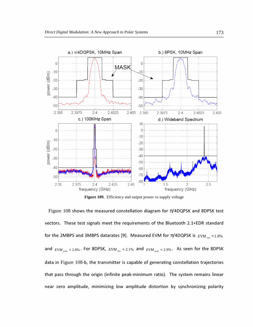
Direct Digital Modulation: A New Approach to Polar Systems 173
Figure 109. Efficiency and output power vs supply voltage
Figure 108 π2(F;&G ;&G
31"#D.?
"1;& <1;& 4-5 .=π2(F;&G %8.1=rmsEVM
%8.2=peakEVM $ ;&G% %1.2=rmsEVM %9.2=peakEVM ;&G
Figure 108%6
)+*
9 % 9 9

Direct Digital Modulation: A New Approach to Polar Systems 174
3
;;?
Quantization noise of the digital modulator is a limiting factor for spectral performance.
Figure 109 a-d.) shows that the nearband spectral requirements for Bluetooth 2.1+EDR
are satisfied for both π/4DQPSK and 8DPSK test signals. Average power levels at the
spectrum analyzer are between 11-14dBm. The wideband spectral mask is satisfied due
to the addition of the bandpass filter at the output. However, it should be noted that in
peak-hold mode, which is required for the Bluetooth standard, there is little margin for
the -40dBm power limit (100kHz RBW). Shown in Figure 109 c.), the lowest margin
occurs near peaks in the quantization noise spectrum 50MHz from the center frequency.
Low margin in the spectral mask could make the system susceptible to load pull, power
supply variation, or other scenarios which cause wideband noise levels to increase. This
can be improved by operating the ∆Σ process at higher clock frequencies, or reducing
transmitter power level. In a fully-integrated version, it may be practical to operate the
∆Σ modulator at 250MHz or more, reducing the peak noise by 3-10dB. Due to limited
margin in meeting the spectral-mask, we do not present this as a fully-functional
Bluetooth transmitter, but rather a demonstration of a new and interesting topology
worthy of further investigation. The high efficiency and excellent linearity show that this
is a promising alternative to traditional Cartesian and polar transmitters.

175
Chapter 7 Conclusion and Future Work
%
C
3
:)*<!>.=6
"> π2(F;&G ;&G 1
39 %
?$39
% :$% :
$% 1
3%39
%
3
+ + 4< 5% 4#!'5%
4#!,5 &% 3 ,
Conclusion and Future Work 176
: %
?$.
+ ; ;
4<-51
C&
? + ' %
8%+ 3
%
6
: :
%6
9
8 +
% % + :
%

177
References
[1] ITRS, "International Technology Roadmap for Semiconductors." Online Reference: www.itrs.net, 2008.
[2] C. H. Doan, S. Emami, D. A. Sobel, A. M. Niknejad, and R. W. Brodersen, "Design considerations for 60GHz radios," IEEE Communications Magazine, vol. 42, pp. 132-140, 2004.
[3] A. A. Abidi, "Direct-conversion radio transceivers for digital communications," IEEE Journal of Solid State Circuits, vol. 30, pp. 1399-1411, Dec. 1995.
[4] F. Montaudon, R. Mina, S. Le Tual, L. Joet, D. Saias, R. Hossain, F. Sibille, C. Corre, V. Carrat, E. Chataigner, J. Lajoinie, S. Dedieu, F. Paillardet, and E. Perea, "A scalable 2.4-to-2.7GHz Wi-Fi/WiMAX discrete-time receiver in 65nm CMOS," IEEE International Solid State Circuits Conference, pp. 362-363, 619, 2008.
[5] R. B. Staszewski, J. Wallberg, S. Rezeq, C.-M. Hung, O. Eliezer, S. Vemulapalli, C. Fernando, K. Maggio, R. Staszewski, N. Barton, M.-C. Lee, P. Cruise, M. Entezari, K. Muhammad, and D. Leipold, "All-digital PLL and GSM/EDGE transmitter in 90nm CMOS," IEEE International Solid State Circuits Conference, vol. 1, pp. 316-600, 2005.
[6] J. T. Stauth and S. R. Sanders, "A 2.4GHz, 20dBm Class-D PA with Single-Bit Digital Polar Modulation in 90nm CMOS," IEEE Custom Integrated Circuits Conference (CICC), 2008.
[7] P. Reynaert and M. Steyaert, RF power amplifiers for mobile communications. Dordrecht: Springer, 2006.
[8] A. J. Viterbi, CDMA : principles of spread spectrum communication. Reading, Mass.: Addison-Wesley Pub. Co., 1995.
[9] Bluetooth_Special_Interests_Group_(SIG), "Bluetooth technical specifications," in www.bluetooth.org, 2008.
[10] T. H. Lee, The design of CMOS radio-frequency integrated circuits, 2nd ed. Cambridge, UK ; New York: Cambridge University Press, 2004.
[11] S. C. Cripps, RF power amplifiers for wireless communications. Boston: Artech House, 1999.
[12] J. L. Dawson and T. H. Lee, Feedback linearization of RF power amplifiers. Boston: Kluwer, 2004.
[13] P. Reynaert and M. Steyaert, "A 1.75-GHz polar modulated CMOS RF power amplifier for GSM-EDGE," IEEE Journal of Solid State Circuits, vol. 40, pp. 2598-2608, Dec. 2005.
[14] A. A. Abidi, "Low-power radio-frequency ICs for portable communications," Proceedings of the IEEE, vol. 83, pp. 544-569, April, 1995.
[15] P. Wambacq and W. M. C. Sansen, Distortion analysis of analog integrated circuits. Boston, Mass: Kluwer Academic, 1998.

References 178
[16] J. Vuolevi and T. Rahkonen, Distortion in RF power amplifiers. Boston: Artech House, 2003.
[17] J. K. Cavers and M. W. Liao, "Adaptive Compensation for Imbalance and Offset Losses in Direct Conversion Transceivers," IEEE Transactions on Vehicular Technology, vol. 42, pp. 581-588, November 1993.
[18] J. Crols and M. Steyaert, CMOS wireless transceiver design. Boston: Kluwer Academic Publishers, 1997.
[19] L. R. Kahn, "Single Sideband Transmission by Envelope Elimination and Restoration," Proceedings IRE, vol. 40, pp. 803-806, July, 1952.
[20] F. H. Raab, S. B.E., R. G. Meyers, and R. M. Jackson, "High efficiency L-band Kahn-technique transmitter," IEEE Microwave Symposium Digest MTT-S, vol. 2, pp. 2220-2225, 1998.
[21] G. Hanington, P.-F. Chen, P. Asbeck, and L. E. Larson, "High-Efficiency Power Amplifier Using Dynamic Power-Supply Voltage for CDMA Applications," IEEE Transactions on Microwave Theory and Techniques, vol. 47, pp. 1471-1476, Aug. 1999.
[22] J. Staudinger, B. Gilsdorf, D. Newman, G. Norris, G. Sadowniczak, R. Sherman, and T. Quach, "High Efficiency CDMA RF Power Amplifier Using Dynamic Envelope Tracking Technique," IEEE Microwave Symposium Digest MTT-S, vol. 2, 2000.
[23] T. Sowlati, D. Rozenblit, R. Pullela, M. Damgaard, E. McCarthy, D. Koh, D. Ripley, F. Balteanu, and I. Gheorghe, "Quad-Band GSM/GPRS/EDGE Polar Loop Transmitter," IEEE Journal of Solid State Circuits, vol. 39 pp. 2179-2189, Dec. 2004.
[24] M. Elliott, T. Montalvo, F. Murden, B. Jeffries, J. Strange, S. Atkinson, A. Hill, S. Nadipaku, and J. Harrebek, "A Polar Modulator Transmitter for EDGE," presented at IEEE Solid States Circuits Conference, San Francisco, CA, 2004.
[25] P. Reynaert and M. Steyaert, "A 1.75GHz GSM/EDGE Polar Modulated CMOS RF Power Amplifier," presented at IEEE Solid State Circuits Conference, San Francisco, 2005.
[26] R. B. Staszewski, J. Wallberg, S. Rezeq, C.-M. Hung, O. Eliezer, S. Vemulapalli, C. Fernando, K. Maggio, R. Staszewski, N. Barton, M.-C. Lee, P. Cruise, M. Entezari, K. Muhammad, and D. Leipold, "All-digital PLL and GSM/EDGE transmitter in 90nm CMOS," IEEE International Solid State Circuits Conference, vol. 1, pp. 316-600, Feb. 2005.
[27] F. Wang, A. H. Yang, D. Kimball, L. E. Larson, and P. Asbeck, "Design of wide-bandwidth envelope tracking power amplifiers for OFDM applications," IEEE Transactions on Microwave Theory and Techniques, vol. 53, pp. 1244-1255, April 2005.
[28] F. Wang, D. Kimball, D. Y. Lie, P. Asbeck, and L. E. Larson, "A Monolithic High-Efficiency 2.4GHz 20dBm SiGe BiCMOS Envelope-Tracking OFDM Power Amplifier," IEEE Journal of Solid State Circuits, vol. 42, pp. 1271-1281, June 2007.
[29] J. T. Stauth and S. R. Sanders, "Power Supply Rejection for Radio Frequency Amplifiers: Theory and Measurements," IEEE Transactions on Microwave Theory and Techniques, vol. 55, pp. 2043-2052, Oct. 2007.
[30] J. T. Stauth and S. R. Sanders, "Power supply rejection for common-source linear RF amplifiers: theory and measurements," IEEE Radio Frequency Integrated Circuits (RFIC) Symposium, pp. 317-320, June 2006.
[31] J. B. Groe and L. E. Larson, CDMA mobile radio design. Boston: Artech House, 2000. [32] F. H. Raab, P. Asbeck, S. Cripps, P. B. Kenington, Z. B. Popovic, N. Pothecary, J. F.
Sevic, and N. O. Sokal, "Power Amplifiers and Transmitters for RF and Microwave," IEEE Transactions on Microwave Theory and Techniques, vol. 50, March 2002.

References 179
[33] I. Aoki, S. D. Kee, D. B. Rutledge, and A. Hajimiri, "Fully Integrated CMOS Power Amplifier Using the Distributed Active-Transformer Architecture," IEEE Journal of Solid State Circuits, vol. 37, 2002.
[34] S. D. Kee, I. Aoki, A. Hajimiri, and D. B. Rutledge, "The Class-E/F Family of ZVS Switching Amplifiers," IEEE Transactions on Microwave Theory and Techniques, vol. 51, 2003.
[35] B. Razavi, RF microelectronics. Upper Saddle River, NJ: Prentice Hall, 1998. [36] J. T. Stauth, "Dynamic Power Supply Design for High-Efficiency Wireless Transmitters,"
in EECS, vol. M.S. . Berkeley, CA: U.C. Berkeley, 2006, pp. 79. [37] A. M. Niknejad, Electromagnetics for high-speed analog and digital communication
circuits. Cambridge, UK ; New York: Cambridge University Press, 2007. [38] G. Liu, P. Haldi, T.-J. King, and A. M. Niknejad, "Fully Integrated CMOS Power
Amplifier With Efficiency Enhancement at Power Back-Off," IEEE Journal of Solid State Circuits, vol. 43, pp. 600-609, March 2008.
[39] P. Haldi, D. Chowdhury, P. Reynaert, G. Liu, and A. M. Niknejad, "A 5.8GHz 1V Linear Power Amplifier Using a Novel On-Chip Transformer Power Combiner in Standard 90nm CMOS," IEEE Journal of Solid State Circuits, vol. 43, pp. 1054-1063, May, 2008.
[40] P. R. Gray, P. J. Hurst, S. H. Lewis, and R. G. Meyer, Analysis and Design of Analog Integrated Circuits, Fourth Edition ed. New York: John Wiley & Sons, 2001.
[41] N. O. Sokal and A. D. Sokal, "Class E - A New Class of High-Efficiency Tuned Single-Ended Switching Power Amplifiers," IEEE Journal of Solid State Circuits, vol. sc-10, pp. 168-176, June 1975.
[42] K.-C. Tsai and P. R. Gray, "A 1.9GHz, 1-W class-E power amplifier for wireless communications," IEEE Journal of Solid State Circuits, vol. 34, pp. 962-970, July 1999.
[43] J. M. Rivas, R. S. Wahby, J. S. Shafran, and D. Perreault, "New Architectures for Radio-Frequency DC-DC Power Conversion," IEEE Transactions on Power Electronics, vol. 21, pp. 380-393, March 2006.
[44] ITRS, "International Technology Roadmap for Semiconductors: http://www.itrs.net," 2006.
[45] A. J. Stratakos, C. R. Sullivan, S. R. Sanders, and R. W. Brodersen, "High-Efficiency Low-Voltage DC-DC Conversion for Portable Applications," in Low-Voltage/Low-Power Integrated Circuits and Systems, E. Sanchez-Sinencio, Ed.: IEEE Press, 1999.
[46] A. P. Chandrakasan, S. Sheng, and R. W. Brodersen, "Low-power CMOS digital design," IEEE Journal of Solid State Circuits, vol. 27, pp. 1415-1428, April 1992.
[47] N. Schlumpf, M. Declercq, and C. Dehollain, "A Fast Modulator for Dynamic Supply Linear RF Power Amplifier," IEEE Journal of Solid State Circuits, vol. 39, July, 2004.
[48] P. Midya, K. Haddad, L. Connel, S. Bergstedt, and B. Roeckner, "Tracking Power Converter for Supply Modulation of RF Power Amplifiers," Power Electronics Specialists Conference (PESC), vol. 3, 2001.
[49] D. Anderson and W. Cantrell, "High Efficiency High Level Modulator for Use in Dynamic Envelope Tracking CDMA RF Power Amplifiers," Microwave Symposium Digest MTT-S, vol. 3, 2001.
[50] B. Sahu and G. A. Rincon-Mora, "A high Efficiency Linear RF Power Amplifier with a Power Tracking Dynamically Adaptive Buck-Boost Supply," IEEE Transactions on Microwave Theory and Techniques, vol. 52, Jan. 2004.
[51] V. Pinon, F. Hasbani, A. Giry, D. Pache, and C. Garnier, "A Single-Chip WCDMA Envelope Reconstruction LDMOS PA with 130MHz Switched-Mode Power Supply," IEEE International Solid State Circuits Conference, vol. 51, pp. 564-565, Feb. 2008.

References 180
[52] E. Alon, J. Kim, S. Pamarti, K. Chang, and M. Horowitz, "Replica compensated linear regulators for supply-regulated phase-locked loops," IEEE Journal of Solid State Circuits, vol. 41, pp. 413-424, Feb. 2006.
[53] V. Gupta and G. A. Rincon-Mora, "A low dropout, CMOS regulator with high PSR over wideband frequencies," IEEE International Symposium on Circuits and Systems (ISCAS), vol. 5, pp. 4245-4248, 2005.
[54] P. K. Hazucha, T., Bloechel, B., Parsons, C., Finan, D., Borkar, S., "Area-efficient linear regulator with ultra-fast load regulation," IEEE Journal of Solid State Circuits, vol. 40, pp. 933-940, April, 2005.
[55] P. T. Krein, Elements of power electronics. New York: Oxford University Press, 1998. [56] J. G. Kassakian, M. F. Schlecht, and G. C. Verghese, Principles of power electronics.
Reading, Mass.: Addison-Wesley, 1991. [57] M. D. seeman and S. R. Sanders, "Analysis and Optimization of Switched-Capacitor DC-
DC Converters," IEEE Transactions on Power Electronics, vol. 23, pp. 841-851, March, 2008.
[58] A. V. Peterchev, "Digital Pulse-Width Modulation Control in Power Electronic Circuits: Theory and Applications," in EECS, vol. PhD. Berkeley: University of California, Berkeley, 2005.
[59] A. V. Peterchev and S. R. Sanders, "Load-line regulation with estimated load-current feedforward: application to microprocessor voltage regulators," IEEE Transactions on Power Electronics, vol. 21, pp. 1704-1717, Nov. 2006.
[60] J. Kitchen, W.-Y. Chu, I. Deligoz, S. Kiaei, and B. Bakkaloglu, "Combined Linear and Delta-Modulated Switched-Mode PA Supply Modulator for Polar Transmitters," IEEE International Solid State Circuits Conference, pp. 82, 588, Feb. 2007.
[61] P. Midya, "Linear Switcher combination with novel feedback," Power Electronics Specialists Conference (PESC), vol. 3, pp. 1425-1429, June 18-23, 2000.
[62] V. Yousefzadeh, E. Alarcon, and D. Maksimovic, "Efficiency optimization in Linear-Assisted switching power converters for envelope tracking in RF power amplifiers," IEEE International Symposium on Circuits and Systems (ISCAS), pp. 1302-1305, May 23-26, 2005.
[63] J. T. Stauth and S. R. Sanders, "Optimum Biasing for Parallel Hybrid Switching-Linear Regulators" IEEE Transactions on Power Electronics, vol. 22, pp. 1978-1985, Sept. 2007.
[64] J. T. Stauth and S. R. Sanders, "Optimum Bias Calculation for Parallel Hybrid Switching-Linear Regulators," Applied Power Electronics Conference (APEC), pp. 569-574, Feb. 2007.
[65] L. O. Chua and N. C.-Y., "Frequency-domain analysis of nonlinear systems: formulation of transfer functions," IEE Journal on Electronic Circuits and Systems, vol. 3, pp. 257-269, 1979.
[66] M. Schetzen, The Volterra and Wiener theories of nonlinear systems. New York: Wiley, 1980.
[67] K. S. Kundert and A. Sangiovanni-Vincentelli, "Simulation of Nonlinear Circuits in the Frequency Domain," IEEE Transactions on Computer-Aided Design of Integrated Circuits and Systems, vol. 5, pp. 521-535, October 1986.
[68] B. Baytekin and R. Meyer, "Analysis and simulation of spectral regrowth in radio frequency power amplifiers," IEEE Journal of Solid State Circuits, vol. 40, pp. 370-381, 2005.

References 181
[69] E. Alon, V. Stojanovic, and M. Horowitz, "Circuits and techniques for high-resolution measurement of on-chip power supply noise," IEEE Journal of Solid State Circuits, vol. 40, pp. 820-828, April, 2005.
[70] D. O. Pederson and K. Mayaram, Analog integrated circuits for communication : principles, simulation, and design. Boston: Kluwer Academic Publishers, 1991.
[71] J. Engberg and T. Larsen, Noise Theory of Linear and Nonlinear Circuits. New Yory: John Wiley and Sons, 1995.
[72] J. Vuolevi and T. Rahkonen, "Analysis of third-order intermodulation distortion in common emitter BJT and HBT amplifiers," IEEE Transactions on Circuits and Systems, vol. 50, pp. 994-1001, 2003.
[73] T. J. Brazil and T. Wang, "Volterra-mapping-based behavioral modeling of nonlinear circuits and systems for high frequencies," IEEE Transactions on Microwave Theory and Techniques, vol. 51, pp. 1433-1440, May 2003.
[74] R. Meyer, "EECS 242 Course Notes," University of California, Berkeley, 2004. [75] J. J. Bussgang, L. Ehrman, and J. W. Graham, "Analysis of Nonlinear Systems with
Multiple Inputs," Proceedings of the IEEE, vol. 62, pp. 1088-1119, 1974. [76] P. Dobrovolny, G. Vandersteen, P. Wambaq, and S. Donnay, "Analysis and compact
behavioral modeling of nonlinear distortion in analog communications circuits," IEEE transactions on Computer-Aided design of integrated circuits and systems, vol. 22, pp. 1215-1227, Sept. 2003.
[77] P. Midya, "Linear Switcher combination with novel feedback," Power Electronics Specialists Conference (PESC), vol. 3, pp. 1425-1429, 2000.
[78] F. Wang, D. Kimball, D. Y. Lie, P. Asbeck, and L. E. Larson, "A Monolithic High-Efficiency 2.4GHz 20dBm SiGe BiCMOS Envelope-Tracking OFDM Power Amplifier," IEEE Journal of Solid State Circuits, vol. 42, pp. 1271-1281, 2007.
[79] V. Yousefzadeh, E. Alarcon, and D. Maksimovic, "Efficiency optimization in Linear-Assisted switching power converters for envelope tracking in RF power amplifiers," IEEE International Symposium on Circuits and Systems (ISCAS), pp. 1302-1305, 2005.
[80] A. V. Peterchev and S. R. Sanders, "Digital multimode buck converter control with loss-minimizing syncronous rectifier adaptation," IEEE Transactions on Power Electronics, vol. 21, pp. 1588-1599, Nov. 2006.
[81] J. Xiao, A. V. Peterchev, J. Zhang, and S. R. Sanders, "A 4-ua quiescent-current dual-mode digitally controlled buck converter IC for cellular phone applications," IEEE Journal of Solid State Circuits, vol. 39, pp. 2342-2348, Dec. 2004.
[82] F. Wang, A. Ojo, D. Kimball, P. Asbeck, and L. E. Larson, "Envelope tracking power amplifier with pre-distoriton linearization for WLAN 802.11g," Microwave Symposium Digest MTT-S, vol. 3, pp. 1543-1546, June 2004.
[83] R. A. R. van der Zee and E. A. van Tuijl, "A power-efficient audio amplifier combining switching and linear techniques," IEEE Journal of Solid State Circuits, vol. 34, pp. 985-991, July 1999.
[84] H. Ertl, J. W. Kolar, and F. C. Zach, "Basic Considerations and Topologies of Switched-Mode Assisted Linear Power Amplifiers," IEEE Transactions on Industrial Electronics, vol. 44, pp. 116-123, February 1997.
[85] T. ido, S. Ishizuka, L. Risbo, F. Aoyagi, and T. Hamasaki, "A digital input controller for audio class-d amplifiers with 100W 0.004% THD+N and 113dB DR," IEEE International Solid State Circuits Conference, vol. 49, pp. 348-349, Feb. 2006.
[86] C. Pascual, Z. Song, P. T. Krein, D. V. Sarwate, P. Midya, and B. Roeckner, "High-Fidelity PWM inverter for digital audio amplification: Spectral analysis, real-time DSP

References 182
implementation, and results," IEEE Transactions on Power Electronics, vol. 18, pp. 473-485, 2003.
[87] J. R. Wells, B. M. Nee, P. L. Chapman, and P. T. Krein, "Selective harmonic control: a general problem formulation and selected solutions," IEEE Transactions on Power Electronics, vol. 20, pp. 1337-1345, 2005.
[88] J. F. Sevic, "Statistical Characterization of RF Power Amplifier Efficiency for CDMA Wireless Communication Systems," Wireless Communications Conference, Proceedings, pp. 110-113, Aug 11-13 1997.
[89] E. McCune, "High-efficiency, multi-mode, multi-band terminal power amplifiers," in IEEE Microwave Magazine, March, 2005, pp. 44-55.
[90] R. Redl and N. O. Sokal, "Near-optimum dynamic regulation of DC-DC converters using feed-forward of output current and input voltage with current-mode control," IEEE Transactions on Power Electronics, vol. PE-1, pp. 181-192, Jul. 1986.
[91] S. Jantzi, R. Schreier, and M. Snelgrove, "Bandpass sigma-delta analog-to-digital conversion," IEEE Transactions on Circuits and Systems, vol. 38, pp. 1406-1409, 1991.
[92] A. Jayaraman, P.-F. Chen, G. Hanington, L. E. Larson, and P. Asbeck, "Linear high-efficiency microwave power amplifiers using bandpass delta-sigma modulators," Microwave and Guided Wave Letters, IEEE, vol. 8, pp. 121-123, 1998.
[93] Y. Wang, "An improved kahn transmitter architecture based on delta-sigma modulation," IEEE International microwave symposium digest, vol. 2, pp. 1327-1330, 2003.
[94] A. Jerng and C. G. Sodini, "A Wideband Delta-Sigma Digital-RF Modulator for High Data Rate Transmitters," IEEE Journal of Solid State Circuits, vol. 42, pp. 1710-1722, Aug. 2007.
[95] C. Berland, I. Hibon, J. F. Bercher, D. Villegas, D. Belot, D. Pache, and V. L. Goascoz, "A transmitter architecture for nonconstant envelope modulation," IEEE Transactions on Circuits and Systems, vol. 53, 2006.
[96] S. M. Taleie, T. Copani, B. Bakkaloglu, and S. Kiaei, "A bandpass Delta-Sigma RF-DAC with embedded FIR reconstruction filter," IEEE International Solid State Circuits Conference (ISSCC) Dig. Tech. Papers, pp. 578-579, 2006.
[97] J. Lindeberg, J. Vanakka, J. Sommarek, and K. Halonen, "A 1.5-V direct digital synthesizer with tunable delta-sigma modulator in 0.12um CMOS," IEEE Journal of Solid State Circuits, vol. 40, pp. 1978-1982, Sept. 2005.
[98] S. Luschas, R. Schreier, and H.-S. Lee, "Radio frequency digital-to-analog converter," IEEE Journal of Solid State Circuits, vol. 39, pp. 1462-1467, 2004.
[99] D. Johns and K. W. Martin, Analog integrated circuit design. New York: John Wiley & Sons, 1997.
[100] A. V. Oppenheim, R. W. Schafer, and J. R. Buck, Discrete-time signal processing, 2nd ed. Upper Saddle River, N.J.: Prentice Hall, 1999.
[101] C. E. Shannon, "Communication in the presence of noise," Proceedings of the Institute of Radio Engineers, vol. 37, pp. 10-21, 1949.
[102] S. R. Norsworthy, R. Schreier, G. C. Temes, and IEEE Circuits and Systems Society., Delta-Sigma data converters : theory, design, and simulation. New York: IEEE Press, 1996.
[103] R. Schreier and G. C. Temes, Understanding delta-sigma data converters. Piscataway, NJ, Hoboken, N.J. ; Chichester: IEEE Press ; Wiley ;, 2005.
[104] D. Anastassiou, "Error Diffusion Coding for A/D Conversion," IEEE Transactions on Circuits and Systems, vol. 36, pp. 1175-1186, 1989.

References 183
[105] A. Kavousian, D. K. Su, and B. A. Wooley, "A Digitally Modulated Polar CMOS PA with 20MHz Signal BW," IEEE International Solid State Circuits Conference (ISSCC) Dig. Tech. Papers, pp. 78-588, 2007.
[106] A. Pozsgay, T. Zounes, R. Hossain, M. Boulemnakher, V. Knopik, and S. Grange, "A Fully Digital 65nm CMOS Transmitter for the 2.4-to-2.7GHz WiFi/WiMAX Bands using 5.4GHz DS RF DACs," IEEE International Solid State Circuits Conference (ISSCC) Dig. Tech. Papers, vol. 51, pp. 360-361, Feb. 2008.
[107] Coilcraft_Inc., "Coilcraft ceramic chip inductors: http://www.coilcraft.com/0805hq.cfm," 2007.
[108] H. Calleja and J. Pacheco, "Power Distribution in Pulse-Density Modulated Waveforms," Power Electronics Specialists Conference (PESC), vol. 3, pp. 1457-1462, 18-23 June 2000.
[109] B. Serneels, T. Piessens, M. Steyaert, and W. Dehaene, "A high-voltage output driver in a 2.5V 0.25um CMOS technology," IEEE Journal of Solid State Circuits, vol. 40, pp. 576-583, March 2005.
[110] Gelb, A. and Vander Velde, W.E., “Multiple-Input Describing Functions and Non-Linear System Design,” McGraw-Hill, New York. 1968.