electrical characterization of graphene and nano-devices€¦ · electrical characterization of...
TRANSCRIPT
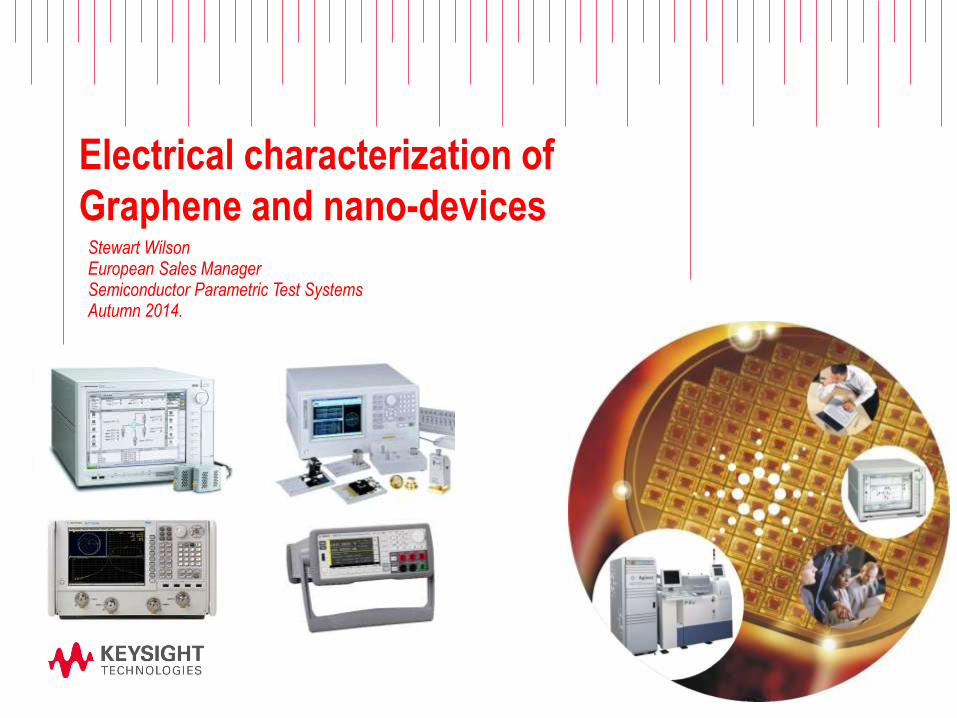
Stewart WilsonEuropean Sales Manager Semiconductor Parametric Test SystemsAutumn 2014.
Electrical characterization of
Graphene and nano-devices
Page
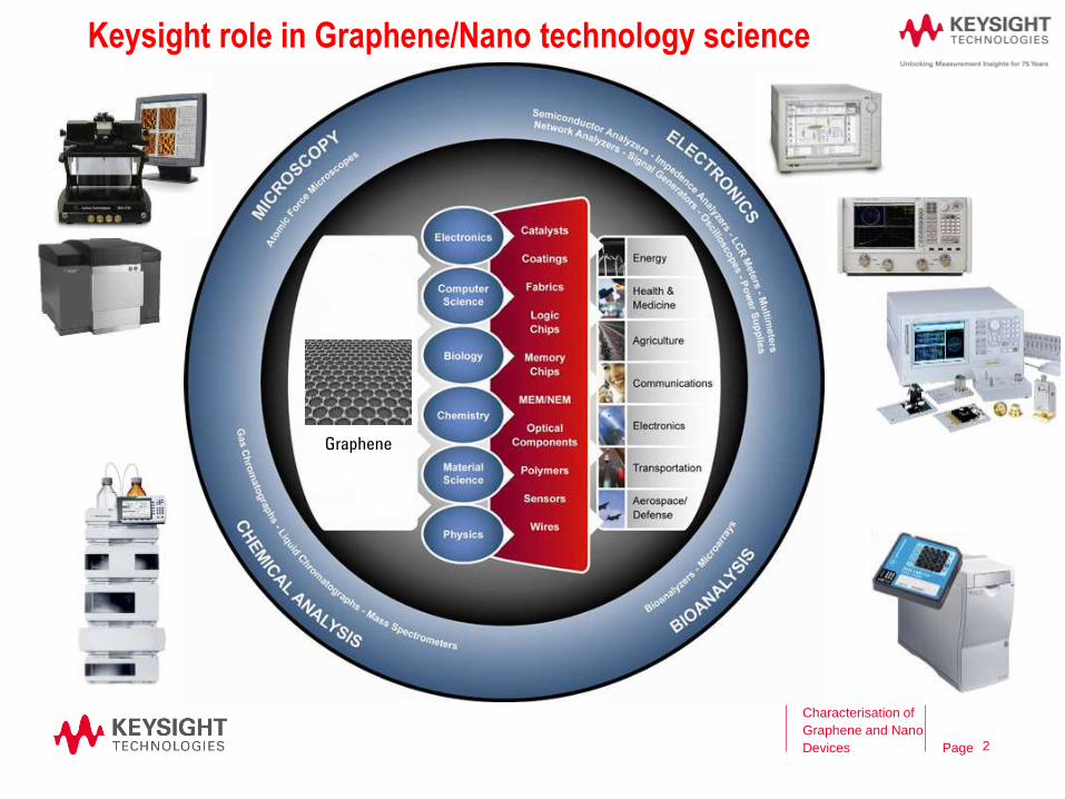
Keysight role in Graphene/Nano technology science
Characterisation of
Graphene and Nano
Devices
Keysight role in Graphene/Nano technology science
Graphene
2
Page
Graphene
Characterisation of
Graphene and Nano
Devices
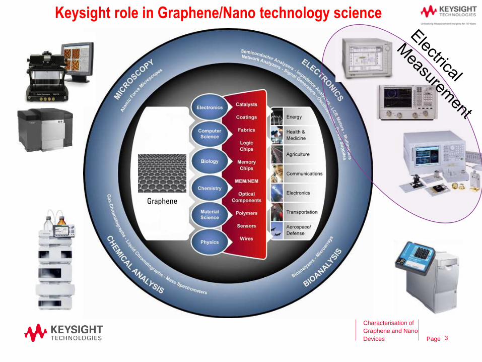
Keysight role in Graphene/Nano technology science
3
Page
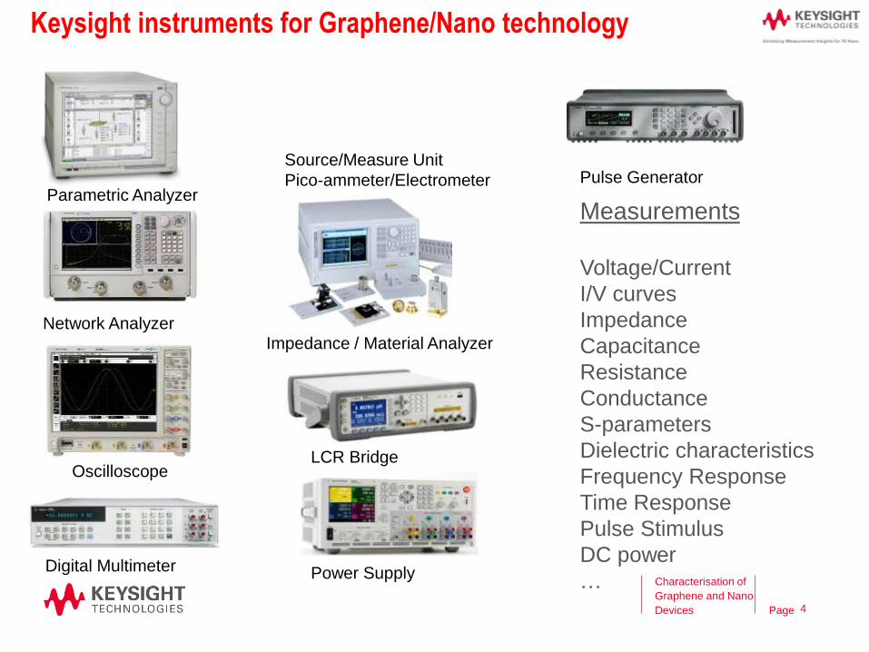
Keysight instruments for Graphene/Nano technology
Parametric Analyzer
Network Analyzer
Impedance / Material Analyzer
Pulse GeneratorSource/Measure Unit
Pico-ammeter/Electrometer
Digital Multimeter
LCR Bridge
Power Supply
Oscilloscope
Measurements
Voltage/Current
I/V curves
Impedance
Capacitance
Resistance
Conductance
S-parameters
Dielectric characteristics
Frequency Response
Time Response
Pulse Stimulus
DC power
… Characterisation of
Graphene and Nano
Devices 4
Page
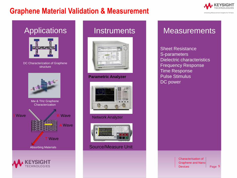
Graphene Material Validation & Measurement
Applications Instruments Measurements
Parametric Analyzer
Network Analyzer
Source/Measure Unit
Sheet Resistance
S-parameters
Dielectric characteristics
Frequency Response
Time Response
Pulse Stimulus
DC power
Absorbing Materials
Mw & THz Graphene
Characterization
DC Characterization of Graphene
structure
I Wave
T Wave
A Wave
R Wave
Characterisation of
Graphene and Nano
Devices 5
Page
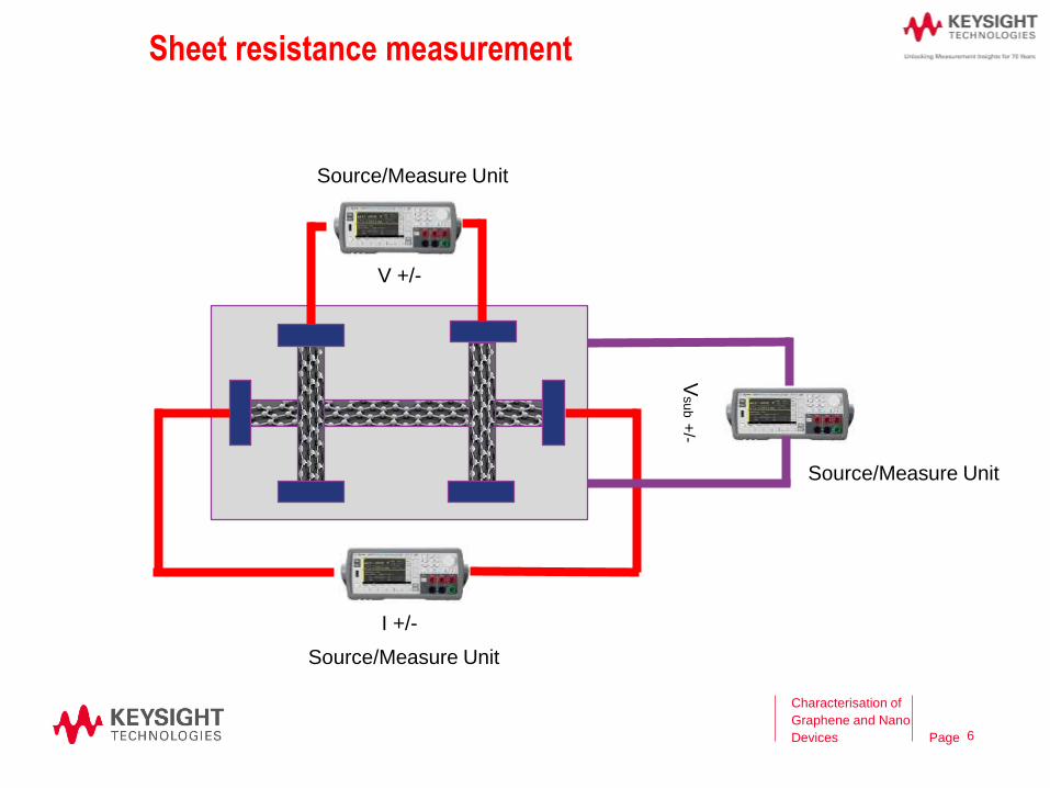
Sheet resistance measurement
V +/-
I +/-
Vsu
b+
/-
Source/Measure Unit
Source/Measure Unit
Source/Measure Unit
Characterisation of
Graphene and Nano
Devices 6
Page
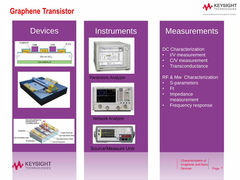
Graphene Transistor
Devices Instruments Measurements
Parametric Analyzer
Network Analyzer
Source/Measure Unit
DC Characterization
• I/V measurement
• C/V measurement
• Transconductance
RF & Mw Characterization
• S-parameters
• Ft
• Impedance
measurement
• Frequency response
Characterisation of
Graphene and Nano
Devices 7
Page
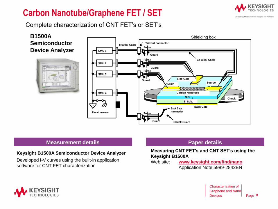
Shielding box
SourceDrain
Side Gate
Si Sub.
SiO 2
Carbon Nanotube
Back Gate
Guard
Co-axial Cable
SMU 1
SMU 2
S
SMU 3
SMU 4
Chuck
Chuck Guard
Back Gate
connectionCircuit common
Guard
Guard
Guard
Force
Force
Force
Force
Triaxial CableTriaxial connector
Carbon Nanotube/Graphene FET / SET
Characterisation of
Graphene and Nano
Devices
Page 8
B1500A
Semiconductor
Device Analyzer
Measurement details Paper details
Keysight B1500A Semiconductor Device Analyzer
Developed I-V curves using the built-in application
software for CNT FET characterization
Measuring CNT FET’s and CNT SET’s using the
Keysight B1500A
Web site: www.keysight.com/find/nano
Application Note 5989-2842EN
Complete characterization of CNT FET’s or SET’s
8

Page
Keysight Parametric Test Solutions
Characterisation of
Graphene and Nano
Devices
B290xA/B291xA Series SMU’s
B2960A Series low noise sources
B2980A Series pico-ammeter/electrometerB1500A Semiconductor
Device Analyzer
B1505A (10kV/ 1500A)
Power Device Analyzer /
Curve Tracer
E5260/70 Modular SMU
ProductsE5250, B220x Switching Matrix
4080 Parametric Tester
Analyzer series
TesterSwitch
Bench top series
Modular
Wide variety of SMU solutions for your semiconductor business
9

Page
Keysight B1500A
Semiconductor Device Analyzer
Parametric measurement solutions
spanning the range from DC to fast
pulsed measurement.
Characterisation
of Graphene and
Nano Devices10
Page
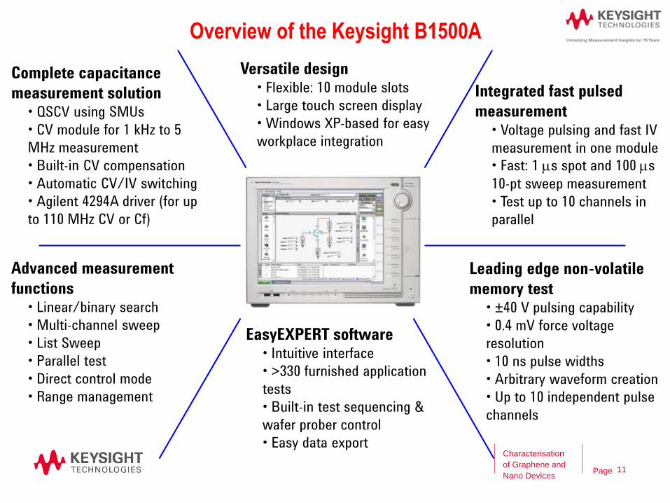
Integrated fast pulsed
measurement• Voltage pulsing and fast IV
measurement in one module
• Fast: 1 ms spot and 100 ms
10-pt sweep measurement
• Test up to 10 channels in
parallel
Overview of the Keysight B1500A
Leading edge non-volatile
memory test• ±40 V pulsing capability
• 0.4 mV force voltage
resolution
• 10 ns pulse widths
• Arbitrary waveform creation
• Up to 10 independent pulse
channels
Complete capacitance
measurement solution• QSCV using SMUs
• CV module for 1 kHz to 5
MHz measurement
• Built-in CV compensation
• Automatic CV/IV switching
• Agilent 4294A driver (for up
to 110 MHz CV or Cf)
Versatile design• Flexible: 10 module slots
• Large touch screen display
• Windows XP-based for easy
workplace integration
EasyEXPERT software• Intuitive interface
• >330 furnished application
tests
• Built-in test sequencing &
wafer prober control
• Easy data export
Advanced measurement
functions• Linear/binary search
• Multi-channel sweep
• List Sweep
• Parallel test
• Direct control mode
• Range management
Characterisation
of Graphene and
Nano Devices11
Page
Characterisation
of Graphene and
Nano Devices
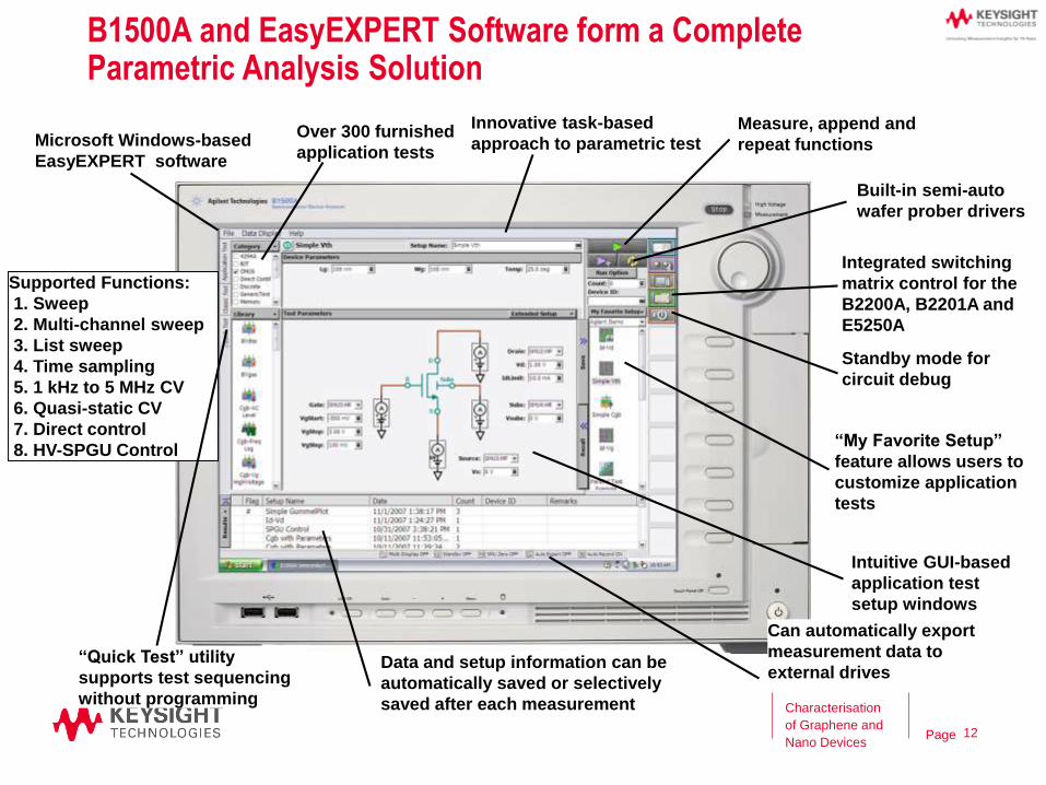
B1500A and EasyEXPERT Software form a CompleteParametric Analysis Solution
Microsoft Windows-based
EasyEXPERT software
Over 300 furnished
application tests
“My Favorite Setup”
feature allows users to
customize application
tests
Data and setup information can be
automatically saved or selectively
saved after each measurement
Intuitive GUI-based
application test
setup windows
Can automatically export
measurement data to
external drives
Measure, append and
repeat functions
Integrated switching
matrix control for the
B2200A, B2201A and
E5250A
Built-in semi-auto
wafer prober drivers
“Quick Test” utility
supports test sequencing
without programming
Innovative task-based
approach to parametric test
Standby mode for
circuit debug
Supported Functions:
1. Sweep
2. Multi-channel sweep
3. List sweep
4. Time sampling
5. 1 kHz to 5 MHz CV
6. Quasi-static CV
7. Direct control
8. HV-SPGU Control
12
Page
Ten slot modular
mainframe
4.2 Amp ground unit
(GNDU)
High power SMU
(HPSMU)
High resolution SMU
(HRSMU)
Medium power SMU
(New MPSMU)
Multi-frequency capacitance
measurement unit (MFCMU)
All SMU types are Kelvin
(separate force and sense inputs)
High-Voltage Semiconductor
Pulse Generator Unit
(HVSPGU)
Waveform Generator/
Fast Measurement Unit
(WGFMU)
Medium Current SMU
(50 µs Pulse MCSMU)
Characterisation
of Graphene and
Nano Devices
B1500A’s Hardware allows both DC and Fast Pulsed Measurements
13

Page
Complete Capacitance
Measurement Solution
Characterisation
of Graphene and
Nano Devices14

Page
B1500A Capacitance Measurement Coverage
5 MHz 110 MHz1 kHz
QSCV
B1500A
(MFCMU)
4294A / E4990A(?)B1500A
(SMU)
HFCV Ultra-HFCV
EasyEXPERT 5.50
• Thin-gate (<2nm)
dielectrics
• Standard (>2nm)
dielectrics
Characterisation
of Graphene and
Nano Devices15
Page
Characterisation
of Graphene and
Nano Devices
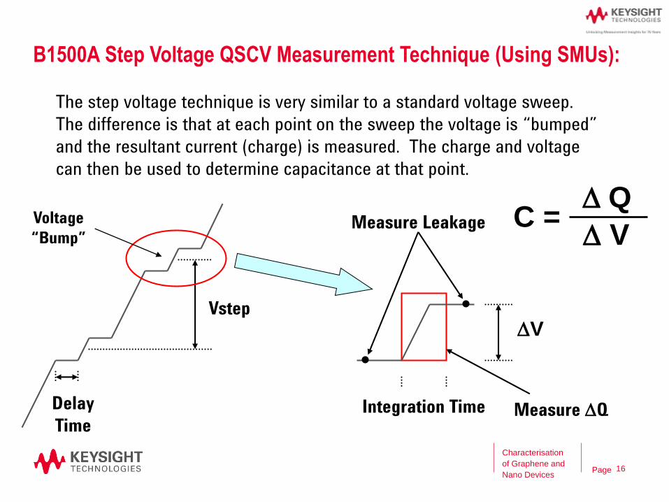
B1500A Step Voltage QSCV Measurement Technique (Using SMUs):
Vstep
Measure Leakage
Delay
Time
DV
Measure DQIntegration Time
C =D V
D Q
The step voltage technique is very similar to a standard voltage sweep.
The difference is that at each point on the sweep the voltage is “bumped”
and the resultant current (charge) is measured. The charge and voltage
can then be used to determine capacitance at that point.
Voltage
“Bump”
16
Page
Characterisation
of Graphene and
Nano Devices
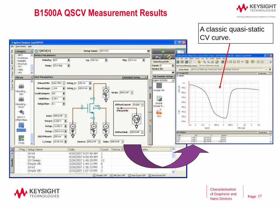
B1500A QSCV Measurement Results
A classic quasi-static
CV curve.
17
Page
Characterisation
of Graphene and
Nano Devices
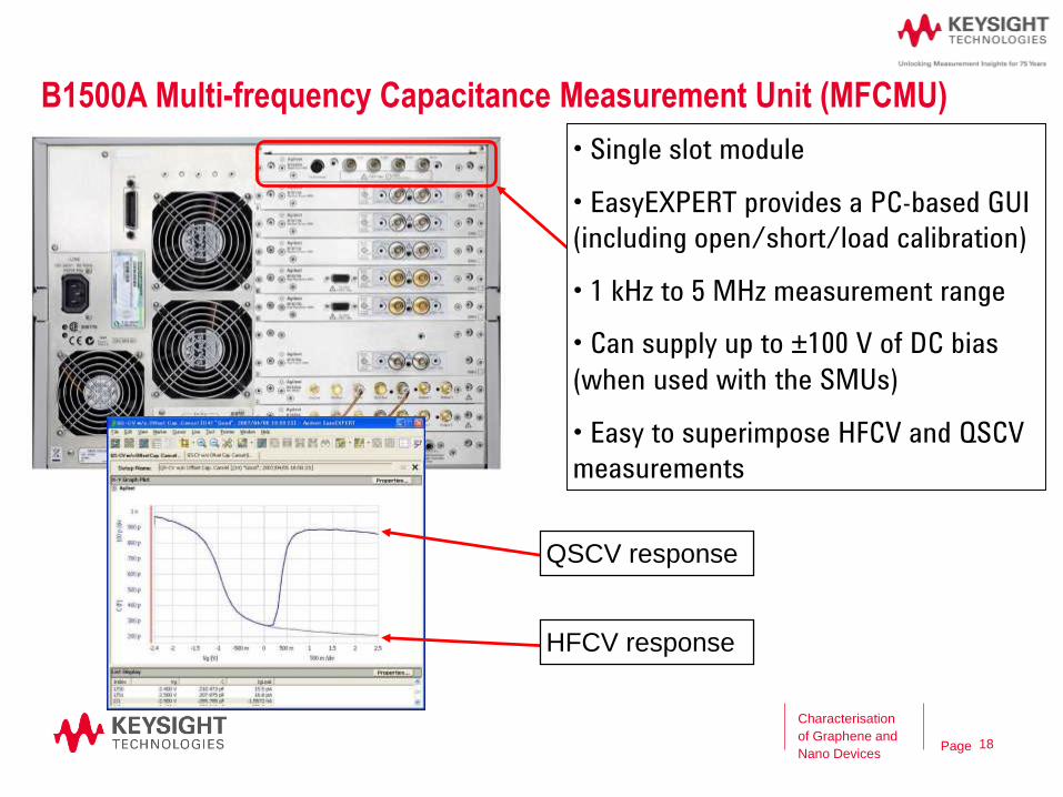
B1500A Multi-frequency Capacitance Measurement Unit (MFCMU)
QSCV response
HFCV response
• Single slot module
• EasyEXPERT provides a PC-based GUI
(including open/short/load calibration)
• 1 kHz to 5 MHz measurement range
• Can supply up to ±100 V of DC bias
(when used with the SMUs)
• Easy to superimpose HFCV and QSCV
measurements
18
Page
Characterisation
of Graphene and
Nano Devices
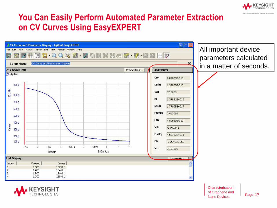
You Can Easily Perform Automated Parameter Extractionon CV Curves Using EasyEXPERT
All important device
parameters calculated
in a matter of seconds.
19

Page
SMU CMU Unify Unit (SCUU) Provides CV-IV Switching and Supports IV Measurements to 1 fA
Outputs converted to
two pairs of triaxial
outputs (Force & Sense)
SMUs
MFCMU
Note: When using the SCUU with the SCUU cable capacitance compensation is
automatic. The cable length is detected at boot-up and built-in compensation
routines compensate to the output of the SCUU.
Characterisation
of Graphene and
Nano Devices20

Page
The B1500A Offers Complete Measurement Coverage –From DC to Ultra-fast Pulsed IV
Measurement Range
Minimum Pulsing capability
1 A
0.1 fA
100us1ms 1us10us 10ns100ns
SMU/MCSMU:
• Technology
development
• Process integration
• Incoming inspection
• Failure analysis
• Reliability test
• Device modeling
• NVM cell test
• Nano device and
material research
• Quasi-static CV
• Timing on-the-fly NBTI
WGFMU:
• Ultra-fast NBTI
• General pulsed IV
• RTS measurement
• Advanced NVM
(PRAM, ReRAM)
• MEMS capacitor
characterization
• All fast time-domain
measurement
B1542A pulsed IV:
• SOI transistor test
• High-k gate
transistor test
Characterisation
of Graphene and
Nano Devices21

Page
What is Driving the Need for Fast Pulsed Measurement?
• New reliability tests (NBTI/PBTI) require spot and sweep
measurements to be made in a few microseconds
• The transient current consumed by memory arrays can be quite
large, and characterizing these current spikes requires current
measurements to be made in one microsecond or less.
• Characterization of SOI MOSFETs requires pulsed measurement
in the nanosecond range to prevent device self-heating effects from
distorting the measurement results
• Characterization of high-k gate dielectric MOSFETs requires
pulsed measurement in the nanosecond range to remove the effects
of electron trapping in the gate oxide due to electron tunneling
•.R&D for novel devices or materials (MEMS, Organic Transistor,
etc.) and many other newly discovered phenomena (such as
random telegraph signal noise) require very fast current and voltage
Characterisation
of Graphene and
Nano Devices22
Page
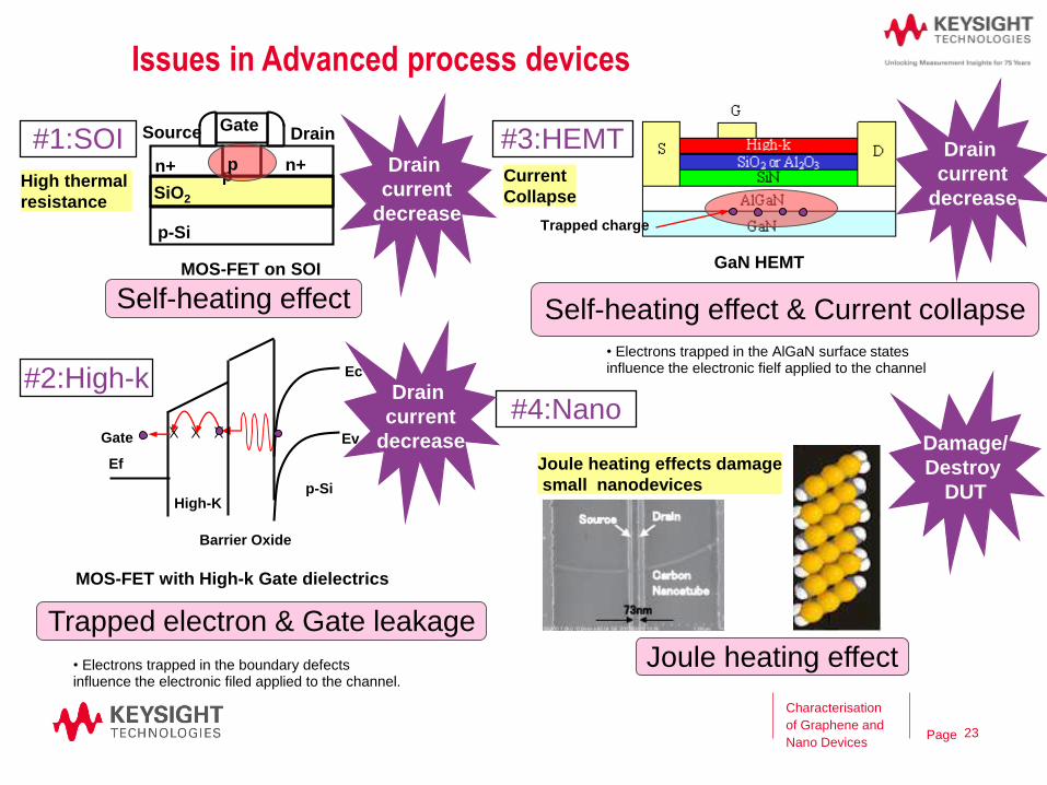
Issues in Advanced process devices
MOS-FET on SOI
n+
p-Si
GateSource Drain
p
Ef
Ev
Ec
Gate
p-Si
Barrier Oxide
High-K
SiO2
n+p
MOS-FET with High-k Gate dielectrics
Self-heating effect
Trapped electron & Gate leakage
#1:SOI
#2:High-k
• Electrons trapped in the boundary defects influence the electronic filed applied to the channel.
High thermal
resistance
#3:HEMT
Self-heating effect & Current collapse
#4:Nano
GaN HEMT
Joule heating effect
Joule heating effects damage
small nanodevices
Trapped charge
Drain
current
decrease
Drain
current
decrease
Drain
current
decrease
Damage/
Destroy
DUT
Current
Collapse
• Electrons trapped in the AlGaN surface states influence the electronic fielf applied to the channel
Characterisation
of Graphene and
Nano Devices23
Page
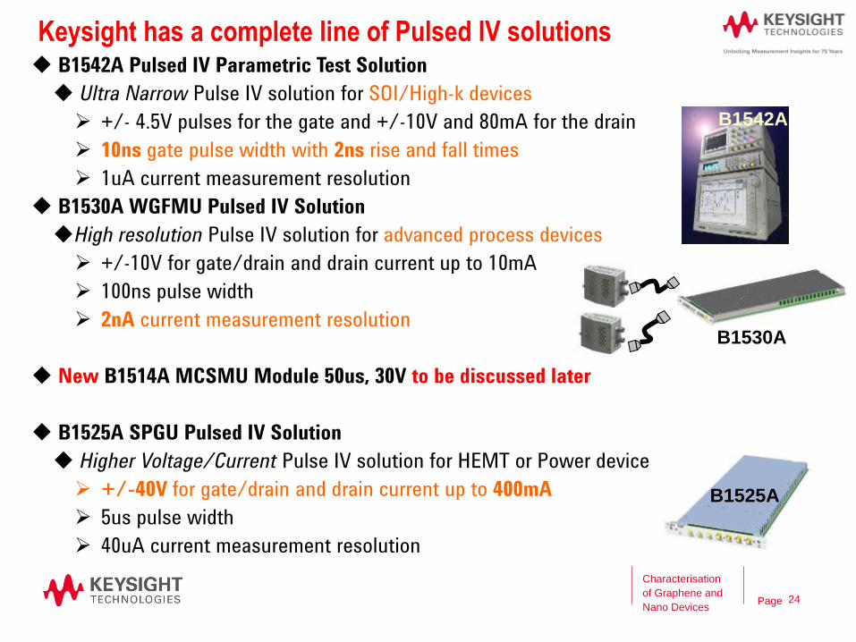
Agilent Pulsed IV solutionsKeysight has a complete line of Pulsed IV solutions B1542A Pulsed IV Parametric Test Solution
Ultra Narrow Pulse IV solution for SOI/High-k devices
+/- 4.5V pulses for the gate and +/-10V and 80mA for the drain
10ns gate pulse width with 2ns rise and fall times
1uA current measurement resolution
B1530A WGFMU Pulsed IV Solution
High resolution Pulse IV solution for advanced process devices
+/-10V for gate/drain and drain current up to 10mA
100ns pulse width
2nA current measurement resolution
New B1514A MCSMU Module 50us, 30V to be discussed later
B1525A SPGU Pulsed IV Solution
Higher Voltage/Current Pulse IV solution for HEMT or Power device
+/-40V for gate/drain and drain current up to 400mA
5us pulse width
40uA current measurement resolution
B1525A
B1530A
B1542A
Characterisation
of Graphene and
Nano Devices24

Page
B1542A Pulsed IV Parametric Test Solution
Target Application
Id-Vd and Id-Vg measurement with pulse “gate” bias for the SOI or high-
k gate dielectrics MOSFET.
Benefits
Ultra narrow pulses reduces the self-heating effects and the
incidence of electron trapping for SOI transistors and high-k gate
dielectric transistors respectively
Capability to apply 10ns gate pulse width with 2ns rise and fall times
Complete package contains all instruments, cables, connectors
and software needed for PIV
System cabling to keep impedance matching for uncluttered pulse shape
down to 10ns pulse width with 2ns rise/fall time
Specially designed Bias-T to make pulse top flat
Feedback loop enables accurate Id-Vd and Id-Vg measurement
Characterisation
of Graphene and
Nano Devices25
Page
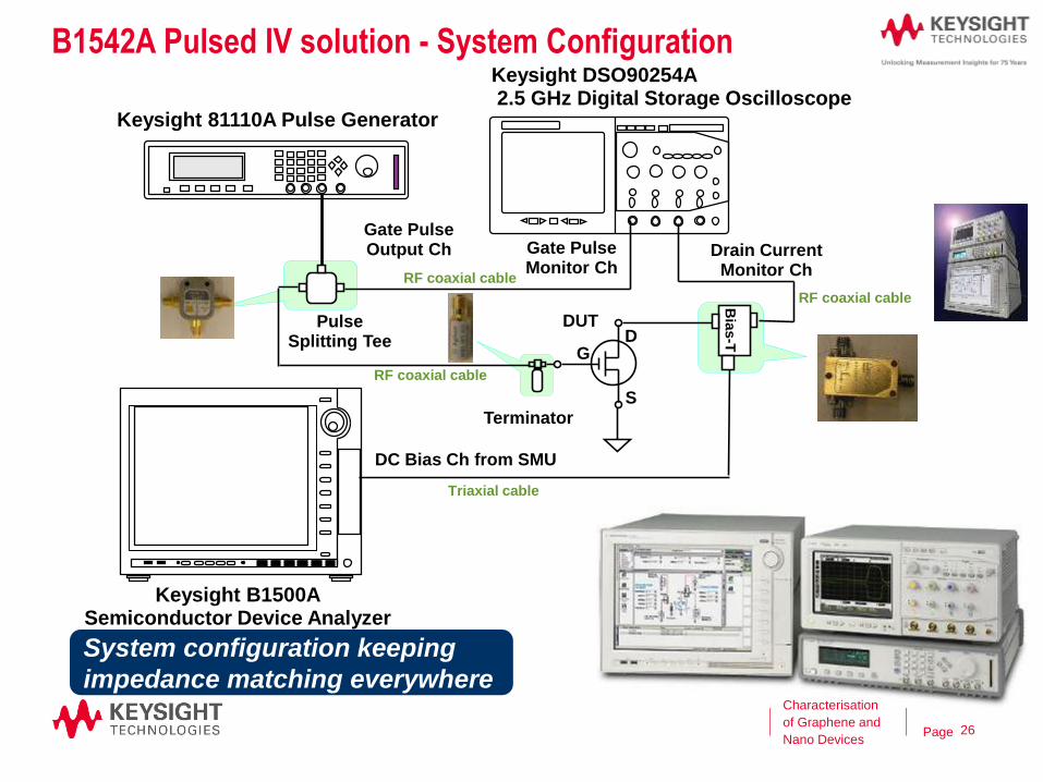
B1542A Pulsed IV solution - System Configuration
Keysight 81110A Pulse Generator
Gate Pulse Monitor Ch
Keysight B1500ASemiconductor Device Analyzer
DC Bias Ch from SMU
Gate Pulse Output Ch
Keysight DSO90254A 2.5 GHz Digital Storage Oscilloscope
D
S
G
Drain Current Monitor Ch
Pulse Splitting Tee
Terminator
Bia
s-T
DUT
Triaxial cable
RF coaxial cable
RF coaxial cable
RF coaxial cable
System configuration keeping
impedance matching everywhereCharacterisation
of Graphene and
Nano Devices26
Page
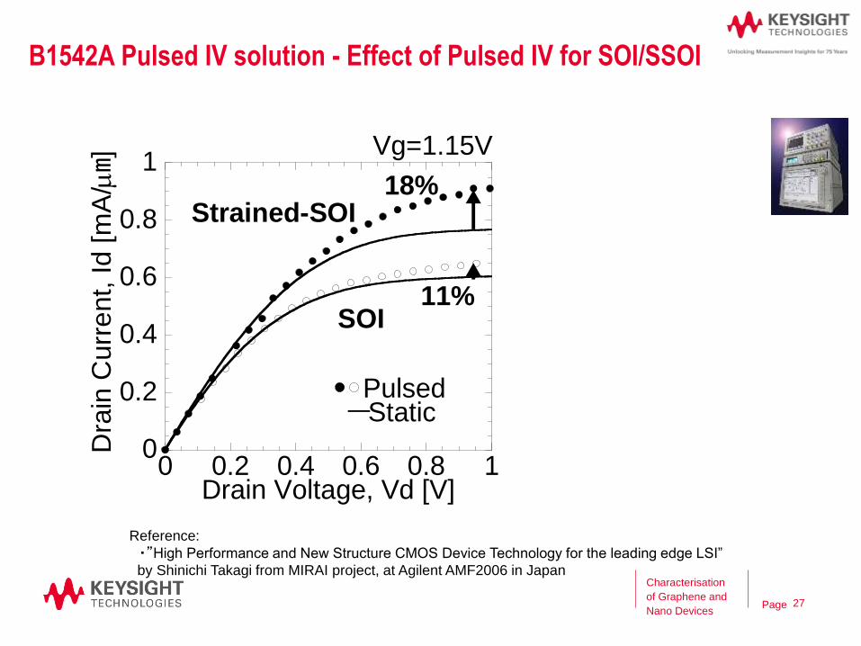
B1542A Pulsed IV solution - Effect of Pulsed IV for SOI/SSOI
0
0.2
0.4
0.6
0.8
1
0 0.2 0.4 0.6 0.8 1
Dra
in C
urr
ent,
Id
[m
A/mm]
Drain Voltage, Vd [V]
Vg=1.15V
StaticPulsed
Strained-SOI18%
11%SOI
Reference:
・”High Performance and New Structure CMOS Device Technology for the leading edge LSI”
by Shinichi Takagi from MIRAI project, at Agilent AMF2006 in Japan Characterisation
of Graphene and
Nano Devices27
Page
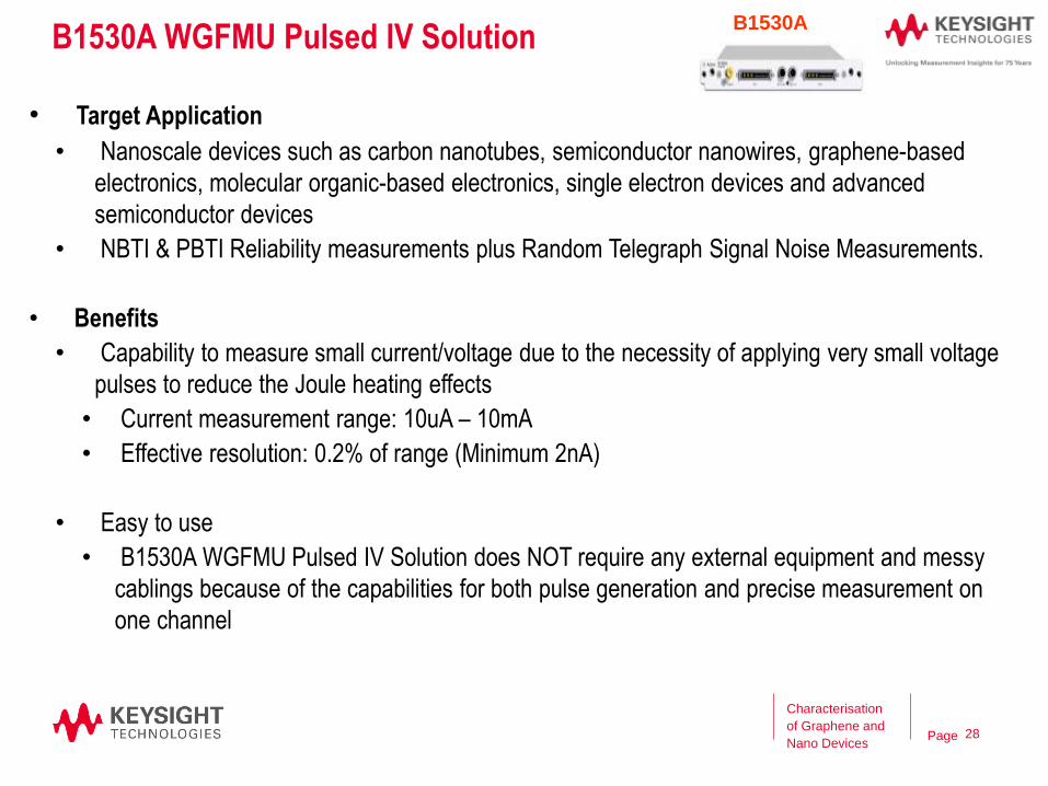
B1530A WGFMU Pulsed IV Solution
• Target Application
• Nanoscale devices such as carbon nanotubes, semiconductor nanowires, graphene-based
electronics, molecular organic-based electronics, single electron devices and advanced
semiconductor devices
• NBTI & PBTI Reliability measurements plus Random Telegraph Signal Noise Measurements.
• Benefits
• Capability to measure small current/voltage due to the necessity of applying very small voltage
pulses to reduce the Joule heating effects
• Current measurement range: 10uA – 10mA
• Effective resolution: 0.2% of range (Minimum 2nA)
• Easy to use
• B1530A WGFMU Pulsed IV Solution does NOT require any external equipment and messy
cablings because of the capabilities for both pulse generation and precise measurement on
one channel
B1530A
Characterisation
of Graphene and
Nano Devices28
Page
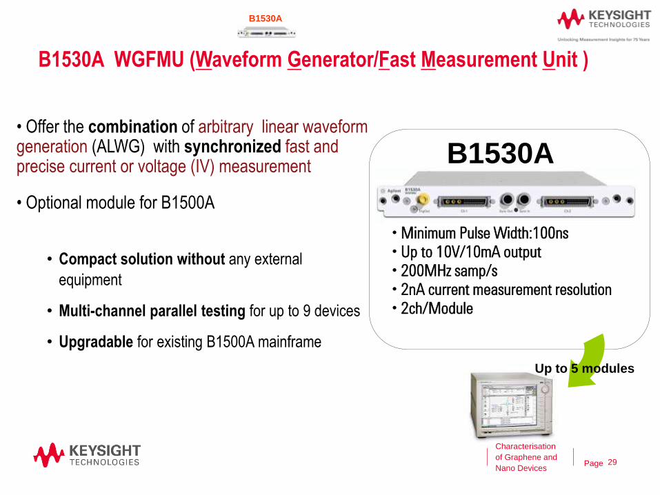
B1530A WGFMU (Waveform Generator/Fast Measurement Unit )
• Offer the combination of arbitrary linear waveform generation (ALWG) with synchronized fast and precise current or voltage (IV) measurement
• Optional module for B1500A
• Compact solution without any external
equipment
• Multi-channel parallel testing for up to 9 devices
• Upgradable for existing B1500A mainframe
B1530A
• Minimum Pulse Width:100ns
• Up to 10V/10mA output
• 200MHz samp/s
• 2nA current measurement resolution
• 2ch/Module
Up to 5 modules
B1530A
Characterisation
of Graphene and
Nano Devices29
Page
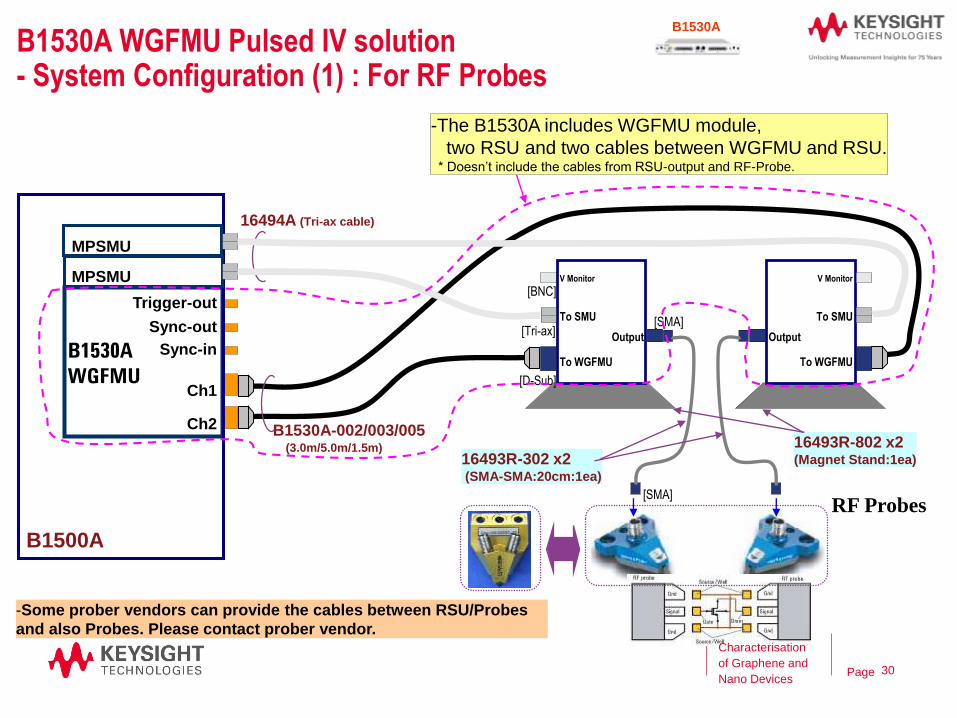
B1530A WGFMU Pulsed IV solution- System Configuration (1) : For RF Probes
B1530A
WGFMU
Trigger-out
Sync-out
Sync-in
Ch1
Ch2
B1500A
B1530A-002/003/005
16493R-302 x2(SMA-SMA:20cm:1ea)
MPSMU
MPSMU
To WGFMU
To SMU
V Monitor
Output
[D-Sub]
[Tri-ax]
[BNC]
To WGFMU
To SMU
V Monitor
Output
[SMA]
[SMA]RF Probes
-The B1530A includes WGFMU module,
two RSU and two cables between WGFMU and RSU.* Doesn’t include the cables from RSU-output and RF-Probe.
16494A (Tri-ax cable)
-Some prober vendors can provide the cables between RSU/Probes
and also Probes. Please contact prober vendor.
16493R-802 x2(Magnet Stand:1ea)
(3.0m/5.0m/1.5m)
B1530A
Characterisation
of Graphene and
Nano Devices30
Page
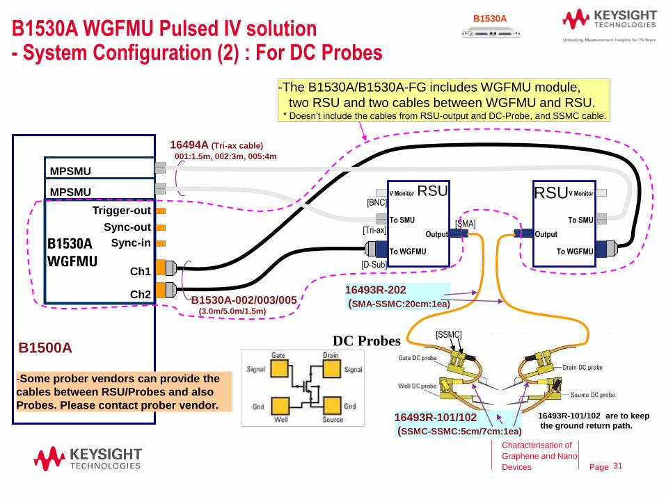
B1530A WGFMU Pulsed IV solution- System Configuration (2) : For DC Probes
B1530A
WGFMU
Trigger-out
Sync-out
Sync-in
Ch1
Ch2
B1500A
B1530A-002/003/00516493R-202
(SMA-SSMC:20cm:1ea)
MPSMU
MPSMU
[D-Sub]
[Tri-ax]
[BNC]
To WGFMU
To SMU
V Monitor
Output
[SMA]
-The B1530A/B1530A-FG includes WGFMU module,
two RSU and two cables between WGFMU and RSU.* Doesn’t include the cables from RSU-output and DC-Probe, and SSMC cable.
16494A (Tri-ax cable)
001:1.5m, 002:3m, 005:4m
[SSMC]
16493R-101/102
(SSMC-SSMC:5cm/7cm:1ea)
To WGFMU
To SMU
V Monitor
Output
RSU RSU
16493R-101/102 are to keep
the ground return path.
-Some prober vendors can provide the
cables between RSU/Probes and also
Probes. Please contact prober vendor.
DC Probes
(3.0m/5.0m/1.5m)
B1530A
Characterisation of
Graphene and Nano
Devices 31
Page
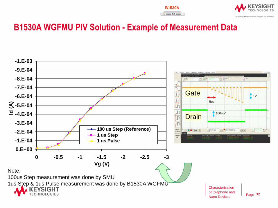
B1530A WGFMU PIV Solution - Example of Measurement Data
-1.E-03
-9.E-04
-8.E-04
-7.E-04
-6.E-04
-5.E-04
-4.E-04
-3.E-04
-2.E-04
-1.E-04
0.E+00
-3-2.5-2-1.5-1-0.50
Vg (V)
Id (
A)
100 us Step (Reference)
1 us Step
1 us Pulse
B1530A
Gate
Drain
Note:
100us Step measurement was done by SMU
1us Step & 1us Pulse measurement was done by B1530A WGFMU
5us
100mV
1V
Characterisation
of Graphene and
Nano Devices32
Page
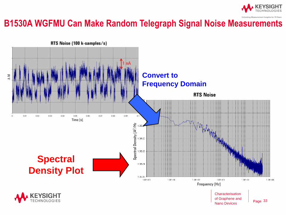
B1530A WGFMU Can Make Random Telegraph Signal Noise Measurements
Convert to
Frequency Domain
Spectral
Density Plot
Characterisation
of Graphene and
Nano Devices33
Page
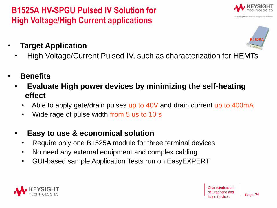
B1525A HV-SPGU Pulsed IV Solution forHigh Voltage/High Current applications
• Target Application
• High Voltage/Current Pulsed IV, such as characterization for HEMTs
• Benefits
• Evaluate High power devices by minimizing the self-heating
effect
• Able to apply gate/drain pulses up to 40V and drain current up to 400mA
• Wide rage of pulse width from 5 us to 10 s
• Easy to use & economical solution
• Require only one B1525A module for three terminal devices
• No need any external equipment and complex cabling
• GUI-based sample Application Tests run on EasyEXPERT
B1525A
Characterisation
of Graphene and
Nano Devices34
Page
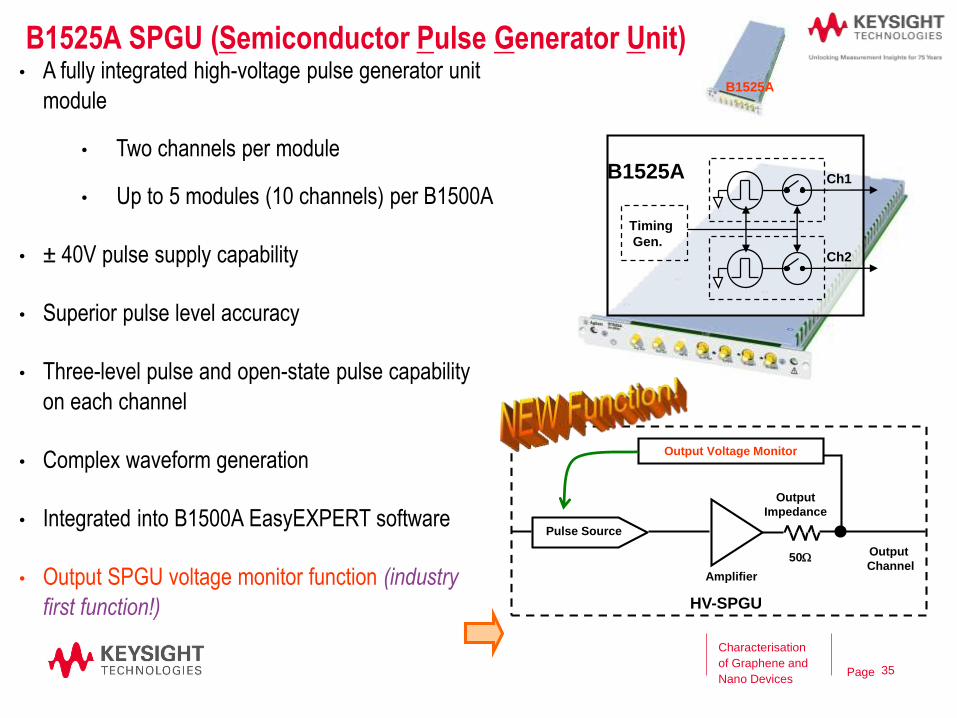
B1525A SPGU (Semiconductor Pulse Generator Unit)• A fully integrated high-voltage pulse generator unit
module
• Two channels per module
• Up to 5 modules (10 channels) per B1500A
• ± 40V pulse supply capability
• Superior pulse level accuracy
• Three-level pulse and open-state pulse capability
on each channel
• Complex waveform generation
• Integrated into B1500A EasyEXPERT software
• Output SPGU voltage monitor function (industry
first function!)
Timing
Gen.
Ch1
Ch2
B1525A
Amplifier
Output
Channel50W
Output
Impedance
Pulse Source
HV-SPGU
Output Voltage Monitor
B1525A
Characterisation
of Graphene and
Nano Devices35

Page
A One Million Cycle Write/Erase Endurance Test Can be Completed in Hours Rather Than Days!
Written Vth
Erased Vth
Written/Erased
Vth Separation
Over Time
% of Write/ Erase
Cycles Completed
is Displayed
Characterisation
of Graphene and
Nano Devices36

Page
All the parameters for Pulsed IV parametric test can be easily set and changed.
B1500A 50 µsec Pulse MCSMU Expands your choice ofPulsed IV up to 30V/1A
• Tracer test mode/OSC view • Application test mode
Oscilloscope view gives you more
confidence for the pulse measurement
of MCSMU by optimizing timing
parameters with monitoring actual V/I
waveform that has been impossible
before
User can optimize the timing
parameters such as integ
time and delay for the best
measurement.
GUI-based dedicated Application test
for pulsed Id-Vd or Id -Vg makes task-
oriented approach also to fast pulsed
IV measurement as easy as 1-2-3.
Characterisation
of Graphene and
Nano Devices37
Page
Parametric Measurement Handbook &Impedance Measurement Handbook Available
You can request it online:
http://www.keysight.com/find/parametrichandbook
http://cp.literature.keysight.com/litweb/pdf/5950-3000.pdf
You can also request a copy by completing the evaluation form.
200+ pages of invaluable
information on parametric test
Characterisation
of Graphene and
Nano Devices38
Page
Characterisation
of Graphene and
Nano Devices
Questions?
39

Page
Thank you for your kind attention
Characterisation
of Graphene and
Nano Devices40