eindhoven university of technology master plasma-deposited
TRANSCRIPT
Eindhoven University of Technology
MASTER
Plasma-deposited polycrystalline siliconfilm growth and characterization
Macco, B.
Award date:2012
Link to publication
DisclaimerThis document contains a student thesis (bachelor's or master's), as authored by a student at Eindhoven University of Technology. Studenttheses are made available in the TU/e repository upon obtaining the required degree. The grade received is not published on the documentas presented in the repository. The required complexity or quality of research of student theses may vary by program, and the requiredminimum study period may vary in duration.
General rightsCopyright and moral rights for the publications made accessible in the public portal are retained by the authors and/or other copyright ownersand it is a condition of accessing publications that users recognise and abide by the legal requirements associated with these rights.
• Users may download and print one copy of any publication from the public portal for the purpose of private study or research. • You may not further distribute the material or use it for any profit-making activity or commercial gain
Plasma-deposited polycrystalline siliconFilm growth and characterization
B. Macco BSc
September 2011 - July 2012PMP 12-07
Department of Applied PhysicsPlasma & Materials Processing (PMP)
Advisors:
dr. K. Sharmadr. M. Creatore
prof.dr.ir. W.M.M. Kessels
deze tekst is alleen zodat het niet lijkt alsof pagina leeg is
Abstract
Polycrystalline silicon thin-film solar cells are considered to be a recognized routefor low-cost photovoltaics. Absorber layers consisting of polycrystalline silicon aim tocombine the high efficiency of wafer-based silicon solar cells with the low-cost manufac-turing typical of thin-film technology. However, polycrystalline silicon solar cells requirea relatively thick absorber layer of typically ∼2 µm, while on the other hand conven-tional deposition techniques like PECVD and HWCVD exhibit a low deposition rate onthe order of 1 nm/s. Therefore, an alternative deposition technique capable of attaininghigh polycrystalline silicon deposition rates, while maintaining a high film quality, ishighly desirable. To this end, the feasibility of depositing polycrystalline silicon by anexpanding thermal plasma (ETP), which has proven to be able to deposit various otherfunctional thin films at high deposition rates (1-60 nm/s), is investigated in this thesis.
The work in this thesis has been guided by three main research topics. First, since thedeposition of polycrystalline silicon was never achieved in ETP, feasibility studies werecarried out. Two approaches for poly-Si deposition were undertaken, i.e. an alternativemethod in which film deposition is alternated with an atomic hydrogen treatment and,secondly, a high-temperature route. The high-temperature route (>600 oC) proved tolead to poly-Si deposition at a deposition rate up to 18 nm/s. Additionally, from thesestudies, the role of growth radicals present in the plasma in poly-Si film deposition hasbeen elucidated.
The second part of the thesis focuses on a fundamental understanding of the devel-opment of crystal grains in poly-Si films. With the use of in-situ and ex-situ charac-terization techniques, various phases of film growth have been identified. It was foundthat the initial film growth consists of an amorphous incubation layer, typically 100-400nm thick. After this thickness, a structural relaxation of the amorphous silicon surfacetakes place due to a build-up of stress, which leads to the formation of crystalline nuclei.From these nuclei, crystalline film growth proceeds in a columnar fashion, with a strongpreferential (220) crystal orientation. Since depositions are carried out at an elevatedtemperature, there is ample thermal energy for the amorphous network in the incubationlayer to relax to the crystalline state, leading to the formation of small randomly-orientedgrains within this incubation layer.
Thirdly, the possibility of applying ETP-deposited poly-Si films in a p-i-n solar cellconfiguration was initiated. For the determination of the optimal poly-Si film proper-ties for solar cell applications, the absorbance of these layers was characterized. Moreprecisely, the role of film thickness and surface roughness in spectral absorbance washighlighted. Additionally, since film roughness is crucial for light trapping purposes,the interplay between deposition conditions and roughness was elucidated. Based onthe developed understanding, a few deposition conditions have been selected for theproduction of p-i-n solar cells in collaboration with the Helmholtz institute in Berlin.
Contents
1 Introduction 41.1 The terawatt challenge . . . . . . . . . . . . . . . . . . . . . . . . . . . . . 41.2 The current status of photovoltaics . . . . . . . . . . . . . . . . . . . . . . 51.3 Thin film crystalline silicon solar cells . . . . . . . . . . . . . . . . . . . . 7
1.3.1 Pathways to poly-Si thin-films . . . . . . . . . . . . . . . . . . . . 81.3.2 Overview of polycrystalline silicon solar cells . . . . . . . . . . . . 121.3.3 Towards higher efficiencies . . . . . . . . . . . . . . . . . . . . . . . 131.3.4 Insights in poly-Si deposition . . . . . . . . . . . . . . . . . . . . . 15
1.4 Research goals and thesis outline . . . . . . . . . . . . . . . . . . . . . . . 17
2 Experimental Setup 192.1 The Expanding Thermal Plasma . . . . . . . . . . . . . . . . . . . . . . . 19
2.1.1 Controlling growth radicals in an Ar-H2-SiH4 plasma . . . . . . . . 212.2 Characterization techniques . . . . . . . . . . . . . . . . . . . . . . . . . . 23
2.2.1 Fourier Transform Infrared Spectroscopy . . . . . . . . . . . . . . . 232.2.2 Raman Spectroscopy . . . . . . . . . . . . . . . . . . . . . . . . . . 272.2.3 Spectroscopic ellipsometry . . . . . . . . . . . . . . . . . . . . . . . 302.2.4 X-ray Diffraction . . . . . . . . . . . . . . . . . . . . . . . . . . . . 312.2.5 UV-VIS Absorbance measurement . . . . . . . . . . . . . . . . . . 36
3 Towards polycrystalline silicon deposition by ETP-CVD 383.1 Introduction . . . . . . . . . . . . . . . . . . . . . . . . . . . . . . . . . . . 383.2 Pulsed deposition for low-temperature crystal growth . . . . . . . . . . . . 393.3 High temperature deposition of polycrystalline silicon . . . . . . . . . . . 42
3.3.1 The role of growth radicals in poly-Si deposition . . . . . . . . . . 453.4 Conclusions . . . . . . . . . . . . . . . . . . . . . . . . . . . . . . . . . . . 47
4 On the growth mechanism of poly-Si deposited by ETP 484.1 Introduction . . . . . . . . . . . . . . . . . . . . . . . . . . . . . . . . . . . 484.2 Experimental details . . . . . . . . . . . . . . . . . . . . . . . . . . . . . . 494.3 Results and discussion . . . . . . . . . . . . . . . . . . . . . . . . . . . . . 49
4.3.1 X-ray diffraction on a poly-Si thickness series . . . . . . . . . . . . 494.3.2 Monitoring poly-Si growth by in-situ SE . . . . . . . . . . . . . . . 50
2
CONTENTS
4.3.3 Proposed growth mechanism . . . . . . . . . . . . . . . . . . . . . 594.4 Conclusions . . . . . . . . . . . . . . . . . . . . . . . . . . . . . . . . . . . 62
5 Optical properties of poly-Si and solar cell performance 635.1 Introduction . . . . . . . . . . . . . . . . . . . . . . . . . . . . . . . . . . . 635.2 Influence of poly-Si thickness and roughness on absorbance . . . . . . . . 645.3 Absorbance of SPC poly-Si films of varying roughness . . . . . . . . . . . 685.4 Effect of deposition conditions on poly-Si roughness . . . . . . . . . . . . 725.5 Solar cell application . . . . . . . . . . . . . . . . . . . . . . . . . . . . . . 745.6 Conclusions . . . . . . . . . . . . . . . . . . . . . . . . . . . . . . . . . . . 75
6 Conclusion and Outlook 776.1 The feasibility of depositing poly-Si by ETP . . . . . . . . . . . . . . . . . 776.2 Crystal growth in ETP-deposited poly-Si . . . . . . . . . . . . . . . . . . 786.3 Optical properties of poly-Si and its application in solar cells . . . . . . . 79
Acknowledgments 80
A Determination of radical fluxes 82A.1 Calculation of silyl flux . . . . . . . . . . . . . . . . . . . . . . . . . . . . 82A.2 Approximating the flux ratio . . . . . . . . . . . . . . . . . . . . . . . . . 82
Bibliography 85
3
Chapter 1
Introduction
1.1 The terawatt challenge
The current world energy consumption, which is at a staggering 15 TW, is dominantlybased on fossil fuels.[1] Over the past decades there has been a growing consensus onthe need to switch to alternative sources of energy, motivated by various factors; Theworld energy consumption is increasing rapidly, which can be attributed in particularto the enormous economic and population growth in India and China. This trend isopposite to the depletion of fossil fuels, particularly oil and natural gas. Additionally,the dependence of (mostly) the Western countries on foreign energy sources poses apolitical risk. And finally, there is the worldwide problem of climate change, whichis induced by the CO2 released during the combustion of fossil fuels. The tragedy ofclimate change is that it mostly affects the developing countries, whereas the rich areresponsible for most of the CO2 production.
The considerations shown above clearly indicate that there is an urgent need foran increased contribution of non-fossil, renewable energy sources to the world energyproduction. In order for renewables to make a significant contribution in the foreseenfuture, their power output will have to increase to the order of terawatts in the next fewdecades: the terawatt challenge.[2]
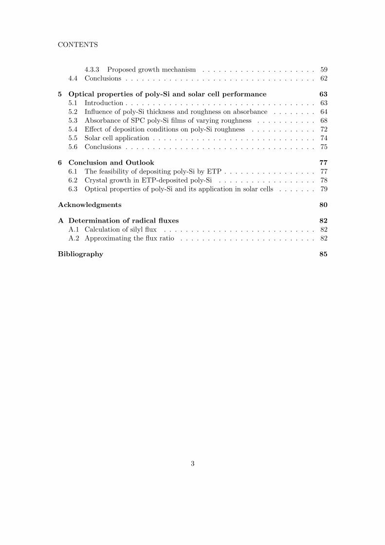
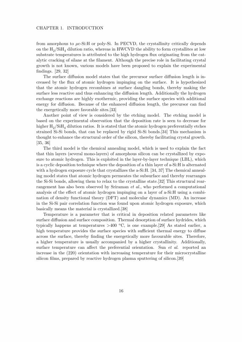
As it can be seen in figure 1.1, the current contribution of renewables to the energymix is minor. Although hydroelectric power is a very cheap and reliable energy source,there has been little increase in its production over the last decade. The simple reasonfor this is that most places where hydroelectric power generation is feasible have alreadybeen exploited. The combustion of biofuels and waste has the largest contribution of therenewables, but it should be noted that this mostly stems from rural cooking activitiesin third-world countries.
Although the contribution of other renewables like geothermal, wind and solar energyis currently negligible, their share will increase in the near future. It has been estimatedthat biomass, wind and geothermal energy can only practically contribute up to 10TW.[3] On the other hand, more than 105 TW of solar power strikes the Earth, of whichit is estimated that 600 TW can technically be harvested.[1] Therefore photovoltaics (PV)
4
CHAPTER 1. INTRODUCTION
8 000
10 000
12 000
14 000
Energy production
IEA Energy Statistics
World
Statistics on the Web: http://www.iea.org/stats/index.asp
0
2 000
4 000
6 000
8 000
1971 1973 1975 1977 1979 1981 1983 1985 1987 1989 1991 1993 1995 1997 1999 2001 2003 2005 2007 2009
Mto
e
Coal/peat Oil Natural gas Nuclear Hydro Biofuels & waste Geothermal/solar/wind
For more detailed data, please consult our on-line data service at http://data.iea.org.© OECD/IEA 2011
Figure 1.1: The global energy production as obtained from the International EnergyAgency website. Mtoe denotes million tonnes of oil equivalent, which is a unit of energy.1 Mtoe ≈ 42 GJ.
is an eligible candidate to meet the terawatt challenge.
1.2 The current status of photovoltaics
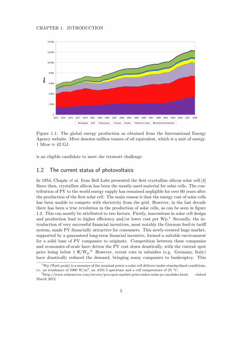
In 1954, Chapin et al. from Bell Labs presented the first crystalline silicon solar cell.[4]Since then, crystalline silicon has been the mostly-used material for solar cells. The con-tribution of PV to the world energy supply has remained negligible for over 60 years afterthe production of the first solar cell. The main reason is that the energy cost of solar cellshas been unable to compete with electricity from the grid. However, in the last decadethere has been a true revolution in the production of solar cells, as can be seen in figure1.2. This can mostly be attributed to two factors. Firstly, innovations in solar cell designand production lead to higher efficiency and/or lower cost per Wp.1 Secondly, the in-troduction of very successful financial incentives, most notably the German feed-in tariffsystem, made PV financially attractive for consumers. This newly-created huge market,supported by a guaranteed long-term financial incentive, formed a suitable environmentfor a solid base of PV companies to originate. Competition between these companiesand economies-of-scale have driven the PV cost down drastically, with the current spotprice being below 1 e/Wp.2 However, recent cuts in subsidies (e.g. Germany, Italy)have drastically reduced the demand, bringing many companies to bankruptcy. This
1Wp (Watt-peak) is a measure of the nominal power a solar cell delivers under standardized conditions,i.e. an irradiance of 1000 W/m2, an AM1.5 spectrum and a cell temperature of 25 oC.
2http://www.solarserver.com/service/pvx-spot-market-price-index-solar-pv-modules.html, visitedMarch 2012
5
CHAPTER 1. INTRODUCTION
demonstrates that PV will need to become cost-competitive (i.e. to achieve grid-parity)without financial incentives.[5]
2 0 0 0 2 0 0 1 2 0 0 2 2 0 0 3 2 0 0 4 2 0 0 5 2 0 0 6 2 0 0 7 2 0 0 8 2 0 0 9 2 0 1 0 2 0 1 1
1 0
2 0
3 0
4 0
5 0
6 0
7 0
Cu
mulat
ive PV
capa
city (G
Wp)
Y e a rFigure 1.2: The global installed PV capacity, as reproduced from the 2011 Market Reportof the EPIA.[6] The figure for 2011 is an estimate.
The major cost of mono- and multicrystalline solar cells resides in the silicon materialuse. The production of crystalline silicon is an energy-intensive process and up to 50% ofthe material is lost during wafer sawing, known as kerf loss. Moreover, wire-sawing cancurrently only obtain thicknesses down to a minimum of 180 µm, whereas only 40 µmis needed for sufficient light absorption. Green et al. calculated that even for a c-Si filmof only 1 µm an efficiency of ∼20% can be obtained when advanced surface passivationand light trapping schemes are employed.[7] This indicates that major advances in theprice/Wp ratio can be made for silicon solar cells by going to thinner films.
Several thin film techniques strive to reduce the cost per Wp by decreasing thematerial consumption. Also, most thin films can be applied on low-cost substrates likepolymer foils, glass and stainless steel. The versatility in substrate material and even theavailability of flexible substrates greatly enhances the applicability of PV, for examplethe integration in buildings and even clothing.
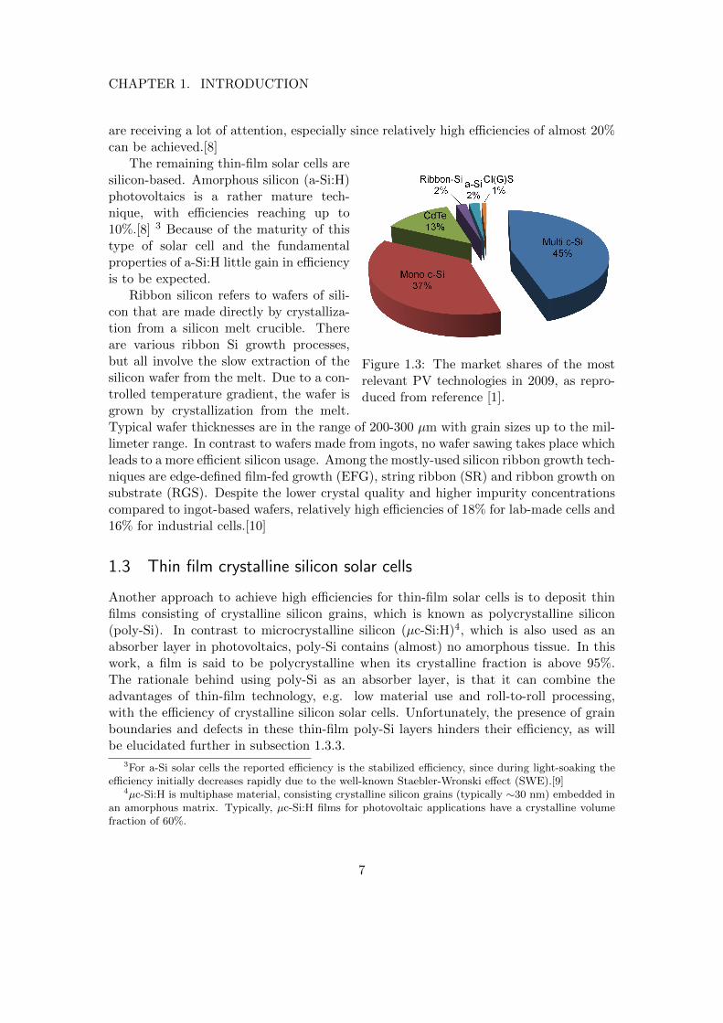
Figure 1.3 shows the market shares of the dominant solar cell types as of 2009.Although the crystalline silicon technologies still have the major market share, thin filmsolar cells have gained momentum in the past decade. Especially CdTe solar cells havea considerable share, although there are environmental concerns because of the use ofthe heavily-toxic cadmium. Also CI(G)S (Copper Indium (Gallium) Sulfide) solar cells
6
CHAPTER 1. INTRODUCTION
are receiving a lot of attention, especially since relatively high efficiencies of almost 20%can be achieved.[8]
Figure 1.3: The market shares of the mostrelevant PV technologies in 2009, as repro-duced from reference [1].
The remaining thin-film solar cells aresilicon-based. Amorphous silicon (a-Si:H)photovoltaics is a rather mature tech-nique, with efficiencies reaching up to10%.[8] 3 Because of the maturity of thistype of solar cell and the fundamentalproperties of a-Si:H little gain in efficiencyis to be expected.
Ribbon silicon refers to wafers of sili-con that are made directly by crystalliza-tion from a silicon melt crucible. Thereare various ribbon Si growth processes,but all involve the slow extraction of thesilicon wafer from the melt. Due to a con-trolled temperature gradient, the wafer isgrown by crystallization from the melt.Typical wafer thicknesses are in the range of 200-300 µm with grain sizes up to the mil-limeter range. In contrast to wafers made from ingots, no wafer sawing takes place whichleads to a more efficient silicon usage. Among the mostly-used silicon ribbon growth tech-niques are edge-defined film-fed growth (EFG), string ribbon (SR) and ribbon growth onsubstrate (RGS). Despite the lower crystal quality and higher impurity concentrationscompared to ingot-based wafers, relatively high efficiencies of 18% for lab-made cells and16% for industrial cells.[10]
1.3 Thin film crystalline silicon solar cells
Another approach to achieve high efficiencies for thin-film solar cells is to deposit thinfilms consisting of crystalline silicon grains, which is known as polycrystalline silicon(poly-Si). In contrast to microcrystalline silicon (µc-Si:H)4, which is also used as anabsorber layer in photovoltaics, poly-Si contains (almost) no amorphous tissue. In thiswork, a film is said to be polycrystalline when its crystalline fraction is above 95%.The rationale behind using poly-Si as an absorber layer, is that it can combine theadvantages of thin-film technology, e.g. low material use and roll-to-roll processing,with the efficiency of crystalline silicon solar cells. Unfortunately, the presence of grainboundaries and defects in these thin-film poly-Si layers hinders their efficiency, as willbe elucidated further in subsection 1.3.3.
3For a-Si solar cells the reported efficiency is the stabilized efficiency, since during light-soaking theefficiency initially decreases rapidly due to the well-known Staebler-Wronski effect (SWE).[9]
4µc-Si:H is multiphase material, consisting crystalline silicon grains (typically ∼30 nm) embedded inan amorphous matrix. Typically, µc-Si:H films for photovoltaic applications have a crystalline volumefraction of 60%.
7

CHAPTER 1. INTRODUCTION
1.3.1 Pathways to poly-Si thin-films
Polycrystalline thin films for solar cells are mainly obtained by three distinct routes:
• Solid phase crystallization (SPC) of a-Si:H
• Direct deposition
• Epitaxial thickening of seed layers
Solid phase crystallization refers to the crystallization of amorphous silicon, a processwhich is activated by thermal energy. Using SPC, poly-Si thin films can be produced ina two-step process, which consists of the deposition of (hydrogenated) amorphous siliconfollowed by thermal annealing at elevated temperatures of typically 600 oC. The crystal-lization process has been schematically drawn in figure 1.4. During the annealing step,the thermal energy allows the amorphous silicon network to relax from its metastablestate to the global minimum of free energy, which corresponds to the crystalline state.
Silicon network configuration
Fre
e e
ne
rgy
crystalline amorphous
Thermal energy
Ga
G
c
Figure 1.4: Schematic of the free energy of the silicon network as a function of itsconfiguration.
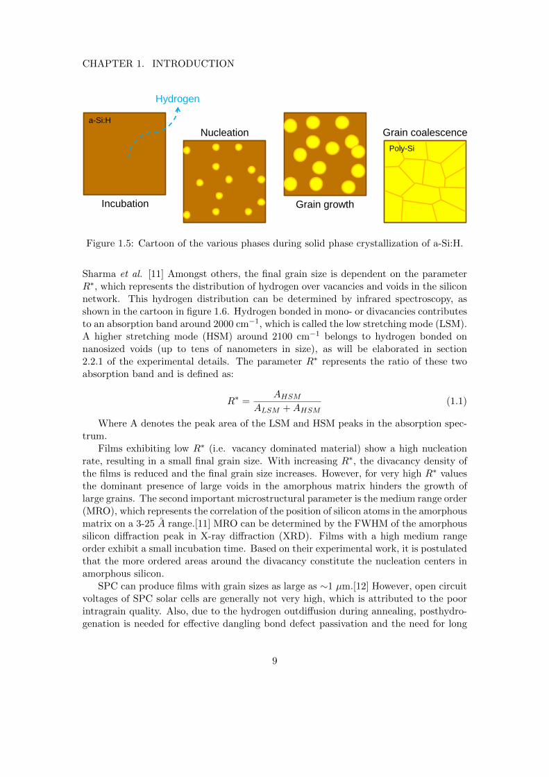
More specifically, the SPC process can be described by various phases, as schemat-ically depicted in figure 1.5. In the incubation phase, hydrogen effuses from the bulkamorphous silicon upon annealing and structural relaxation of the silicon network takesplace. After the so-called incubation time, small randomly oriented nuclei of crystallinesilicon appear homogeneously in the bulk of the matrix, that subsequently grow in thegrain growth phase until the grains coalesce and the film is entirely crystalline.
The SPC process has already been studied in great detail, and a clear correlationbetween the film microstructure, incubation time and final grain size has been found by
8
CHAPTER 1. INTRODUCTION
Hydrogen
Incubation
Nucleation
Grain growth
Grain coalescence
a-Si:H
Poly-Si
Figure 1.5: Cartoon of the various phases during solid phase crystallization of a-Si:H.
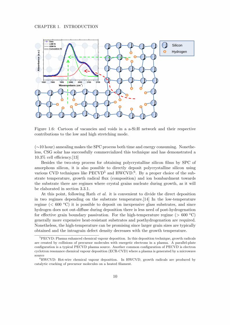
Sharma et al. [11] Amongst others, the final grain size is dependent on the parameterR∗, which represents the distribution of hydrogen over vacancies and voids in the siliconnetwork. This hydrogen distribution can be determined by infrared spectroscopy, asshown in the cartoon in figure 1.6. Hydrogen bonded in mono- or divacancies contributesto an absorption band around 2000 cm−1, which is called the low stretching mode (LSM).A higher stretching mode (HSM) around 2100 cm−1 belongs to hydrogen bonded onnanosized voids (up to tens of nanometers in size), as will be elaborated in section2.2.1 of the experimental details. The parameter R∗ represents the ratio of these twoabsorption band and is defined as:
R∗ =AHSM
ALSM +AHSM(1.1)
Where A denotes the peak area of the LSM and HSM peaks in the absorption spec-trum.
Films exhibiting low R∗ (i.e. vacancy dominated material) show a high nucleationrate, resulting in a small final grain size. With increasing R∗, the divacancy density ofthe films is reduced and the final grain size increases. However, for very high R∗ valuesthe dominant presence of large voids in the amorphous matrix hinders the growth oflarge grains. The second important microstructural parameter is the medium range order(MRO), which represents the correlation of the position of silicon atoms in the amorphousmatrix on a 3-25 A range.[11] MRO can be determined by the FWHM of the amorphoussilicon diffraction peak in X-ray diffraction (XRD). Films with a high medium rangeorder exhibit a small incubation time. Based on their experimental work, it is postulatedthat the more ordered areas around the divacancy constitute the nucleation centers inamorphous silicon.
SPC can produce films with grain sizes as large as ∼1 µm.[12] However, open circuitvoltages of SPC solar cells are generally not very high, which is attributed to the poorintragrain quality. Also, due to the hydrogen outdiffusion during annealing, posthydro-genation is needed for effective dangling bond defect passivation and the need for long
9
CHAPTER 1. INTRODUCTION
Silicon
Hydrogen
1850 1900 1950 2000 2050 2100 2150
A
bs
orb
an
ce
(a
.u.)
Wavenumbers (cm-1)
Data
LSM fit
HSM fit
Cumulative fit
Figure 1.6: Cartoon of vacancies and voids in a a-Si:H network and their respectivecontributions to the low and high stretching mode.
(∼10 hour) annealing makes the SPC process both time and energy consuming. Nonethe-less, CSG solar has successfully commercialized this technique and has demonstrated a10.3% cell efficiency.[13]
Besides the two-step process for obtaining polycrystalline silicon films by SPC ofamorphous silicon, it is also possible to directly deposit polycrystalline silicon usingvarious CVD techniques like PECVD5 and HWCVD.6. By a proper choice of the sub-strate temperature, growth radical flux (composition) and ion bombardment towardsthe substrate there are regimes where crystal grains nucleate during growth, as it willbe elaborated in section 3.3.1.
At this point, following Rath et al. it is convenient to divide the direct depositionin two regimes depending on the substrate temperature.[14] In the low-temperatureregime (< 600 oC) it is possible to deposit on inexpensive glass substrates, and sincehydrogen does not out-diffuse during deposition there is less need of post-hydrogenationfor effective grain boundary passivation. For the high-temperature regime (> 600 oC)generally more expensive heat-resistant substrates and posthydrogenation are required.Nonetheless, the high-temperature can be promising since larger grain sizes are typicallyobtained and the intragrain defect density decreases with the growth temperature.
5PECVD: Plasma enhanced chemical vapour deposition. In this deposition technique, growth radicalsare created by collisions of precursor molecules with energetic electrons in a plasma. A parallel-plateconfiguration is a typical PECVD plasma source. Another common configuration of PECVD is electroncyclotron resonance chemical vapour deposition (ECR-CVD) where a plasma is generated by a microwavesource
6HWCVD: Hot-wire chemical vapour deposition. In HWCVD, growth radicals are produced bycatalytic cracking of precursor molecules on a heated filament.
10
CHAPTER 1. INTRODUCTION
substrate
Crystal growth
Crystal nucleation Amorphous incubation layer
Grain coalescence
Figure 1.7: Schematic of the various phases of film growth typically associated withpoly-Si film growth.
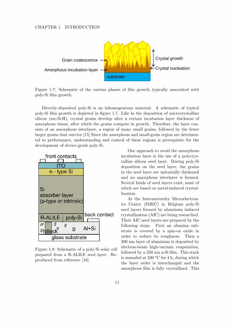
Directly-deposited poly-Si is an inhomogeneous material. A schematic of typicalpoly-Si film growth is depicted in figure 1.7. Like in the deposition of microcrystallinesilicon (mc-Si:H), crystal grains develop after a certain incubation layer thickness ofamorphous tissue, after which the grains compete in growth. Therefore, the layer con-sists of an amorphous interlayer, a region of many small grains, followed by the fewerlarger grains that survive.[15] Since the amorphous and small-grain region are detrimen-tal to performance, understanding and control of these regions is prerequisite for thedevelopment of device-grade poly-Si.
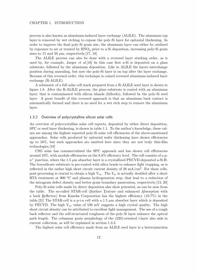
Figure 1.8: Schematic of a poly-Si solar cellprepared from a R-ALILE seed layer. Re-produced from reference [16].
One approach to avoid the amorphousincubation layer is the use of a polycrys-talline silicon seed layer. During poly-Sideposition on the seed layer, the grainsin the seed layer are epitaxially thickenedand no amorphous interlayer is formed.Several kinds of seed layers exist, most ofwhich are based on metal-induced crystal-lization.
At the Interuniversity Microelectron-ics Centre (IMEC) in Belgium poly-Siseed layers formed by aluminum inducedcrystallization (AIC) are being researched.Their AIC seed layers are prepared by thefollowing steps. First an alumina sub-strate is covered by a spin-on oxide inorder to reduce its roughness. Then a200 nm layer of aluminum is deposited byelectron-beam high-vacuum evaporation,followed by a 250 nm a-Si film. This stackis annealed at 500 oC for 4 h, during whichthe layer order is interchanged and theamorphous film is fully crystallized. This
11
CHAPTER 1. INTRODUCTION
process is also known as aluminum-induced layer exchange (ALILE). The aluminum toplayer is removed by wet etching to expose the poly-Si layer for epitaxial thickening. Inorder to improve the final poly-Si grain size, the aluminum layer can either be oxidizedby exposure to air or treated by HNO3 prior to a-Si deposition, increasing poly-Si grainsizes to 15 and 50 µm, respectively.[17, 18]
The ALILE process can also be done with a reversed layer stacking order, as isused by, for example, Jaeger et al.[16] In this case first a-Si is deposited on a glasssubstrate, followed by the aluminum deposition. Like in ALILE the layers interchangeposition during annealing, but now the poly-Si layer is on top after the layer exchange.Because of this reversed order, this technique is coined reversed aluminum-induced layerexchange (R-ALILE).
A schematic of a full solar cell stack prepared from a R-ALILE seed layer is shown infigure 1.8. After the R-ALILE process, the glass substrate is coated with an aluminumlayer, that is contaminated with silicon islands (hillocks), followed by the poly-Si seedlayer. A great benefit of this reversed approach is that an aluminum back contact isautomatically formed and there is no need for a wet etch step to remove the aluminumlayer.
1.3.2 Overview of polycrystalline silicon solar cells
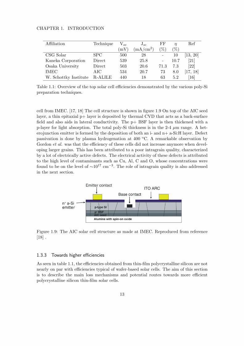
An overview of polycrystalline solar cell reports, deposited by either direct deposition,SPC or seed layer thickening, is shown in table 1.1. To the author’s knowledge, these val-ues are among the highest reported poly-Si solar cell efficiencies of the above-mentionedapproaches. Solar cells produced by epitaxial wafer thickening have shown efficienciesup to 16%, but such approaches are omitted here since they are not truly thin-filmtechnologies.[19]
CSG solar has commercialized the SPC approach and has shown cell efficienciesaround 10%, with module efficiencies on the 8.8% efficiency level. The cell consists of a p-n+ junction, where the 1.5 µm absorber layer is a crystallized PECVD-deposited a-Si:H.The borosilicate substrate is pre-coated with silica beads to enhance light trapping, as isreflected in the rather high short circuit current density of 28 mA/cm2. For these cells,post-processing is crucial to obtain a high Voc. The Voc is actually doubled after a shortRTA treatment at 900 oC and plasma hydrogenation step, that lead to a reduction ofthe intragrain defect density and better grain boundary passivation, respectively.[13, 20]
Poly-Si solar cells made by direct deposition also show potential, as can be seen fromthe table. The so-called STAR-cell (Surface Texture and enhanced Absorption witha back Reflector) from Kaneka Corporation has the highest efficiency (10.7%) in thetable.[21] The STAR-cell is a p-i-n cell with a 1.5 µm absorber layer which is depositedby PECVD. The high Voc value of 539 mV suggests a high crystal quality. The highshort circuit density can be attributed to excellent light management. The use of a roughback reflector and the self-structured roughness of the poly-Si layer enhance the opticalpath length. The columnar grain morphology of the (220)-oriented i-layer also aids incurrent collection, as will be explained in section 1.3.3.
The highest solar cell efficiency made from an ALILE seed layer is a heterojunction
12
CHAPTER 1. INTRODUCTION
Affiliation Technique Voc Jsc FF η Ref(mV) (mA/cm2) (%) (%)
CSG Solar SPC 500 28 - 10 [13, 20]Kaneka Corporation Direct 539 25.8 - 10.7 [21]Osaka University Direct 503 20.6 71.3 7.3 [22]IMEC AIC 534 20.7 73 8.0 [17, 18]W. Schottky Institute R-ALILE 440 18 63 5.2 [16]
Table 1.1: Overview of the top solar cell efficiencies demonstrated by the various poly-Sipreparation techniques.
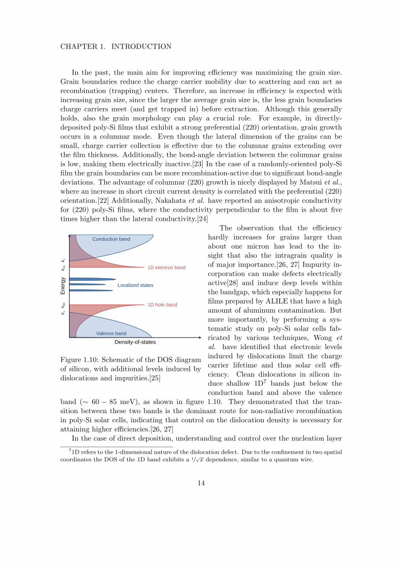
cell from IMEC. [17, 18] The cell structure is shown in figure 1.9 On top of the AIC seedlayer, a thin epitaxial p+ layer is deposited by thermal CVD that acts as a back-surfacefield and also aids in lateral conductivity. The p+ BSF layer is then thickened with ap-layer for light absorption. The total poly-Si thickness is in the 2-4 µm range. A het-erojunction emitter is formed by the deposition of both an i- and n+ a-Si:H layer. Defectpassivation is done by plasma hydrogenation at 400 oC. A remarkable observation byGordon et al. was that the efficiency of these cells did not increase anymore when devel-oping larger grains. This has been attributed to a poor intragrain quality, characterizedby a lot of electrically active defects. The electrical activity of these defects is attributedto the high level of contaminants such as Cu, Al, C and O, whose concentrations werefound to be on the level of ∼1017 cm−3. The role of intragrain quality is also addressedin the next section.
Figure 1.9: The AIC solar cell structure as made at IMEC. Reproduced from reference[18] .
1.3.3 Towards higher efficiencies
As seen in table 1.1, the efficiencies obtained from thin-film polycrystalline silicon are notnearly on par with efficiencies typical of wafer-based solar cells. The aim of this sectionis to describe the main loss mechanisms and potential routes towards more efficientpolycrystalline silicon thin-film solar cells.
13
CHAPTER 1. INTRODUCTION
In the past, the main aim for improving efficiency was maximizing the grain size.Grain boundaries reduce the charge carrier mobility due to scattering and can act asrecombination (trapping) centers. Therefore, an increase in efficiency is expected withincreasing grain size, since the larger the average grain size is, the less grain boundariescharge carriers meet (and get trapped in) before extraction. Although this generallyholds, also the grain morphology can play a crucial role. For example, in directly-deposited poly-Si films that exhibit a strong preferential (220) orientation, grain growthoccurs in a columnar mode. Even though the lateral dimension of the grains can besmall, charge carrier collection is effective due to the columnar grains extending overthe film thickness. Additionally, the bond-angle deviation between the columnar grainsis low, making them electrically inactive.[23] In the case of a randomly-oriented poly-Sifilm the grain boundaries can be more recombination-active due to significant bond-angledeviations. The advantage of columnar (220) growth is nicely displayed by Matsui et al.,where an increase in short circuit current density is correlated with the preferential (220)orientation.[22] Additionally, Nakahata et al. have reported an anisotropic conductivityfor (220) poly-Si films, where the conductivity perpendicular to the film is about fivetimes higher than the lateral conductivity.[24]
En
erg
y
Density-of-states
Conduction band
Valence band
1D electron band
1D hole band
Localized states
Ec
ED
e
Ev
ED
h
Figure 1.10: Schematic of the DOS diagramof silicon, with additional levels induced bydislocations and impurities.[25]
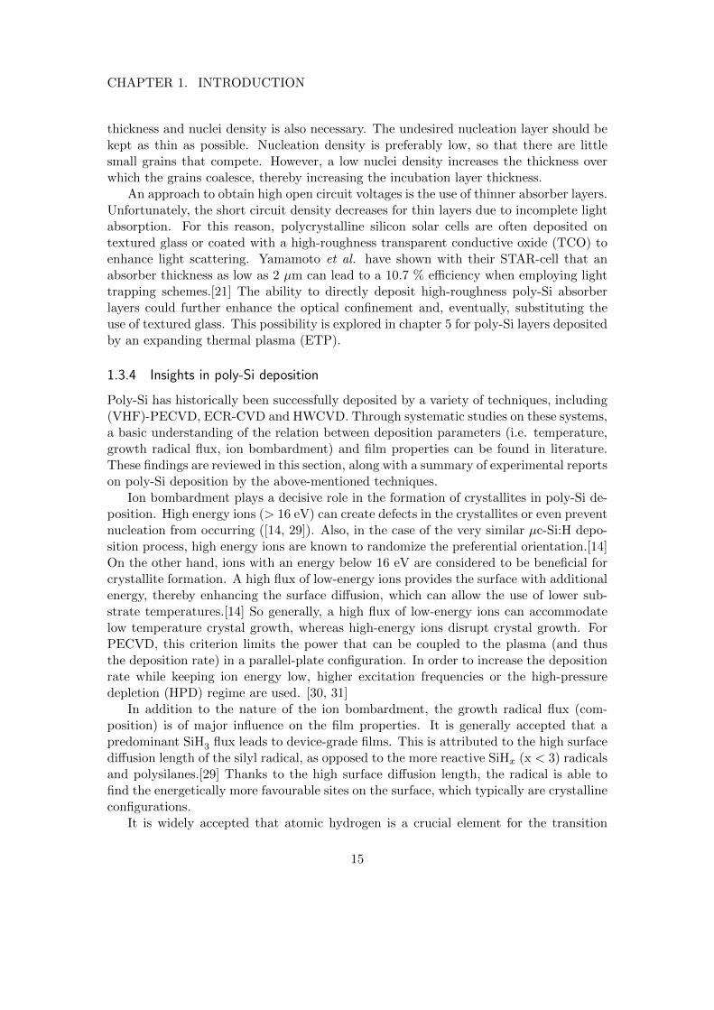
The observation that the efficiencyhardly increases for grains larger thanabout one micron has lead to the in-sight that also the intragrain quality isof major importance.[26, 27] Impurity in-corporation can make defects electricallyactive[28] and induce deep levels withinthe bandgap, which especially happens forfilms prepared by ALILE that have a highamount of aluminum contamination. Butmore importantly, by performing a sys-tematic study on poly-Si solar cells fab-ricated by various techniques, Wong etal. have identified that electronic levelsinduced by dislocations limit the chargecarrier lifetime and thus solar cell effi-ciency. Clean dislocations in silicon in-duce shallow 1D7 bands just below theconduction band and above the valence
band (∼ 60 − 85 meV), as shown in figure 1.10. They demonstrated that the tran-sition between these two bands is the dominant route for non-radiative recombinationin poly-Si solar cells, indicating that control on the dislocation density is necessary forattaining higher efficiencies.[26, 27]
In the case of direct deposition, understanding and control over the nucleation layer
71D refers to the 1-dimensional nature of the dislocation defect. Due to the confinement in two spatialcoordinates the DOS of the 1D band exhibits a 1/
√E dependence, similar to a quantum wire.
14
CHAPTER 1. INTRODUCTION
thickness and nuclei density is also necessary. The undesired nucleation layer should bekept as thin as possible. Nucleation density is preferably low, so that there are littlesmall grains that compete. However, a low nuclei density increases the thickness overwhich the grains coalesce, thereby increasing the incubation layer thickness.
An approach to obtain high open circuit voltages is the use of thinner absorber layers.Unfortunately, the short circuit density decreases for thin layers due to incomplete lightabsorption. For this reason, polycrystalline silicon solar cells are often deposited ontextured glass or coated with a high-roughness transparent conductive oxide (TCO) toenhance light scattering. Yamamoto et al. have shown with their STAR-cell that anabsorber thickness as low as 2 µm can lead to a 10.7 % efficiency when employing lighttrapping schemes.[21] The ability to directly deposit high-roughness poly-Si absorberlayers could further enhance the optical confinement and, eventually, substituting theuse of textured glass. This possibility is explored in chapter 5 for poly-Si layers depositedby an expanding thermal plasma (ETP).
1.3.4 Insights in poly-Si deposition
Poly-Si has historically been successfully deposited by a variety of techniques, including(VHF)-PECVD, ECR-CVD and HWCVD. Through systematic studies on these systems,a basic understanding of the relation between deposition parameters (i.e. temperature,growth radical flux, ion bombardment) and film properties can be found in literature.These findings are reviewed in this section, along with a summary of experimental reportson poly-Si deposition by the above-mentioned techniques.
Ion bombardment plays a decisive role in the formation of crystallites in poly-Si de-position. High energy ions (> 16 eV) can create defects in the crystallites or even preventnucleation from occurring ([14, 29]). Also, in the case of the very similar µc-Si:H depo-sition process, high energy ions are known to randomize the preferential orientation.[14]On the other hand, ions with an energy below 16 eV are considered to be beneficial forcrystallite formation. A high flux of low-energy ions provides the surface with additionalenergy, thereby enhancing the surface diffusion, which can allow the use of lower sub-strate temperatures.[14] So generally, a high flux of low-energy ions can accommodatelow temperature crystal growth, whereas high-energy ions disrupt crystal growth. ForPECVD, this criterion limits the power that can be coupled to the plasma (and thusthe deposition rate) in a parallel-plate configuration. In order to increase the depositionrate while keeping ion energy low, higher excitation frequencies or the high-pressuredepletion (HPD) regime are used. [30, 31]
In addition to the nature of the ion bombardment, the growth radical flux (com-position) is of major influence on the film properties. It is generally accepted that apredominant SiH3 flux leads to device-grade films. This is attributed to the high surfacediffusion length of the silyl radical, as opposed to the more reactive SiHx (x < 3) radicalsand polysilanes.[29] Thanks to the high surface diffusion length, the radical is able tofind the energetically more favourable sites on the surface, which typically are crystallineconfigurations.
It is widely accepted that atomic hydrogen is a crucial element for the transition
15
CHAPTER 1. INTRODUCTION
from amorphous to µc-Si:H or poly-Si. In PECVD, the crystallinity critically dependson the H2/SiH4 dilution ratio, whereas in HWCVD the ability to form crystallites at lowsubstrate temperatures is attributed to the high hydrogen flux originating from the cat-alytic cracking of silane at the filament. Although the precise role in facilitating crystalgrowth is not known, various models have been proposed to explain the experimentalfindings. [29, 32]
The surface diffusion model states that the precursor surface diffusion length is in-creased by the flux of atomic hydrogen impinging on the surface. It is hypothesizedthat the atomic hydrogen recombines at surface dangling bonds, thereby making thesurface less reactive and thus enhancing the diffusion length. Additionally the hydrogenexchange reactions are highly exothermic, providing the surface species with additionalenergy for diffusion. Because of the enhanced diffusion length, the precursor can findthe energetically more favorable sites.[33]
Another point of view is considered by the etching model. The etching model isbased on the experimental observation that the deposition rate is seen to decrease forhigher H2/SiH4 dilution ratios. It is stated that the atomic hydrogen preferentially etchesstrained Si-Si bonds, that can be replaced by rigid Si-Si bonds.[34] This mechanism isthought to enhance the structural order of the silicon, thereby facilitating crystal growth.[35, 36]
The third model is the chemical annealing model, which is used to explain the factthat thin layers (several mono-layers) of amorphous silicon can be crystallized by expo-sure to atomic hydrogen. This is exploited in the layer-by-layer technique (LBL), whichis a cyclic deposition technique where the deposition of a thin layer of a-Si:H is alternatedwith a hydrogen exposure cycle that crystallizes the a-Si:H. [34, 37] The chemical anneal-ing model states that atomic hydrogen permeates the subsurface and thereby rearrangesthe Si-Si bonds, allowing them to relax to the crystalline state.[32] This structural rear-rangement has also been observed by Sriraman et al., who performed a computationalanalysis of the effect of atomic hydrogen impinging on a layer of a-Si:H using a combi-nation of density functional theory (DFT) and molecular dynamics (MD). An increasein the Si-Si pair correlation function was found upon atomic hydrogen exposure, whichbasically means the material is crystallized.[38]
Temperature is a parameter that is critical in deposition related parameters likesurface diffusion and surface composition. Thermal desorption of surface hydrides, whichtypically happens at temperatures >400 oC, is one example.[29] As stated earlier, ahigh temperature provides the surface species with sufficient thermal energy to diffuseacross the surface, thereby finding the energetically more favourable sites. Therefore,a higher temperature is usually accompanied by a higher crystallinity. Additionally,surface temperature can affect the preferential orientation. Sun et al. reported anincrease in the (220) orientation with increasing temperature for their microcrystallinesilicon films, prepared by reactive hydrogen plasma sputtering of silicon.[39]
16
CHAPTER 1. INTRODUCTION
1.4 Research goals and thesis outline
In this thesis, the possibility of using an ETP for polycrystalline silicon deposition is ex-plored. The expanding thermal plasma has been extensively investigated in our group,both in terms of the Ar-SiH4-H2 plasma chemistry and in terms of the deposition ofhydrogenated amorphous silicon (a-Si:H) and µc-Si:H. But despite being a well-studieddeposition system, no experimental conditions resulting in the deposition of polycrys-talline silicon are known to date.
Nonetheless, the expanding thermal plasma may prove to be a promising tool forpoly-Si deposition. Compared to other deposition techniques, the ETP generally hasa higher deposition rate (e.g. several tens of nm/s for a-Si:H). Given the relativelylow poly-Si deposition rate of typically a few nm/s or less for conventional depositiontechniques, along with the required absorber thickness of several microns for photovoltaicapplications, the advantages of achieving a high deposition rate by ETP are evident.
On the other hand, the deposition of poly-Si at high deposition rates with an ETPwill probably prove to be challenging. The ETP is known to deliver a very little amountof ion bombardment (i.e. ion energies <2-3 eV), especially when molecular hydrogen isadmixed in the arc (as will be explained in section 2.1). The absence of ion bombardmentfor providing additional energy to the surface for surface diffusion, along with a highdeposition rate will make it hard to achieve crystal growth.
The feasibility of depositing poly-Si with an ETP is the topic of chapter 3. The mainresearch questions that are addressed are:
• Is it possible to deposit poly-Si with an expanding thermal plasma?
• How do growth radicals affect the film phase?
• Can a high deposition rate be achieved?
To this end, two approaches for poly-Si deposition have been explored. The firstone consists of depositing using a pulsed silane flow in order to alternate depositionwith hydrogen treatment. The effect of the hydrogen treatment, which is thought toincrease film crystallinity, is investigated. The second approach consists of depositionsin the high-temperature regime (> 600 oC). For these depositions, the dependence offilm properties like crystallinity and resistance to oxidation on the growth radicals issystematically studied.
Chapter 4 focuses on the growth mechanism of crystal grains in our poly-Si films.The main research topics in this chapter are:
• How do crystal grains develop during deposition? Do the poly-Si films have anincubation layer like in µc-Si:H and if so, how is it controlled by the depositionparameters?
• How does the preferential crystal orientation depend on deposition parameters?Can films with the beneficial (220) orientation be deposited? Does the preferential
17
CHAPTER 1. INTRODUCTION
orientation prevail from the start of crystalline film growth or does it develop overthe film thickness?
To answer these questions films have been analyzed both by ex-situ and in-situ char-acterization techniques. Ex-situ XRD analysis on a series of films of different thicknesseshas been used to investigate the evolution of the crystallite properties during deposition.In-situ spectroscopic ellipsometry (SE) has been used for real-time monitoring of thefilm thickness and roughness. Additionally, in-situ SE allows for the investigation of thepresence of an amorphous incubation layer. By combining the results of these studies,a growth model for poly-Si growth in our setup is presented, which has been verified byTEM imaging.
Since it is planned to produce p-i-n solar cells from our poly-Si films, their opticalabsorbance should be considered as well. Therefore, the following topics are addressedin chapter 5:
• How does the film absorbance depend on the film thickness? What thickness wouldbe needed for the application in a p-i-n solar cell?
• Can poly-Si films with a native texture be deposited? And if so, what is the effectof the film roughness on light trapping?
• Which deposition parameters influence the film roughness? Can we understandwhy?
• Is it possible to produce p-i-n solar cells from the deposited poly-Si films? How dosolar cell parameters (η, Voc, Jsc and FF) depend on the properties of the intrinsicpoly-Si absorber layer?
These questions are addressed in three parts of the chapter. In the first part, theabsorbance of a thickness series of poly-Si films is measured to determine the effect offilm thickness and roughness on absorbance. The effect of roughness on absorbance hasbeen further clarified by comparison of the absorbance of a series of 1 µm SPC poly-Siof variable surface roughness. In the second part, the role of deposition parameters onsurface roughness has been investigated by performing a detailed AFM analysis andand the rationale behind the observed trends is presented. The last part is on theproduction of p-i-n solar cells using an intrinsic poly-Si absorber layer deposited byETP, in a collaboration with the Helmholtz institute in Berlin. Unfortunately, theseexperiments are still underway. Therefore, an overview of the planned depositions ispresented, along with a motivation for the chosen deposition conditions.
In the following chapter the experimental setup is described. A detailed descriptionof the expanding thermal plasma deposition setup is given, along with the accompanyingAr-H2-SiH4 plasma chemistry. Additionally, the experimental techniques adopted duringthese studies are explained.
18
Chapter 2
Experimental Setup
In this chapter the experimental setup used for deposition will be discussed, along withthe most used analysis techniques. First the ETP setup is described, including theAr-H2-SiH4 plasma chemistry in the ETP. In subsequent sections fourier transform in-frared spectroscopy (FTIR), Raman spectroscopy, XRD, SE and the UV-VIS absorbancesetup are treated in detail, since these analysis techniques have been extensively usedthroughout the project.
2.1 The Expanding Thermal Plasma
The ETP is a plasma enhanced chemical vapor deposition (PECVD) technique that hasbeen developed at the Eindhoven University of Technology. It has been shown thatthe ETP setup is a very viable tool for the deposition of various functional thin films,especially for solar cell applications. Among these are a-Si:H[40] and mc-Si:H[41] filmsas solar cell absorber layers, silicon nitride (a-SiNx:H) films as antireflection coating[42],silicon oxide (SiO2) as a surface passivation layer[43] and aluminum-doped zinc oxide(ZnO:Al) acting as a transparent conductive oxide.[44]
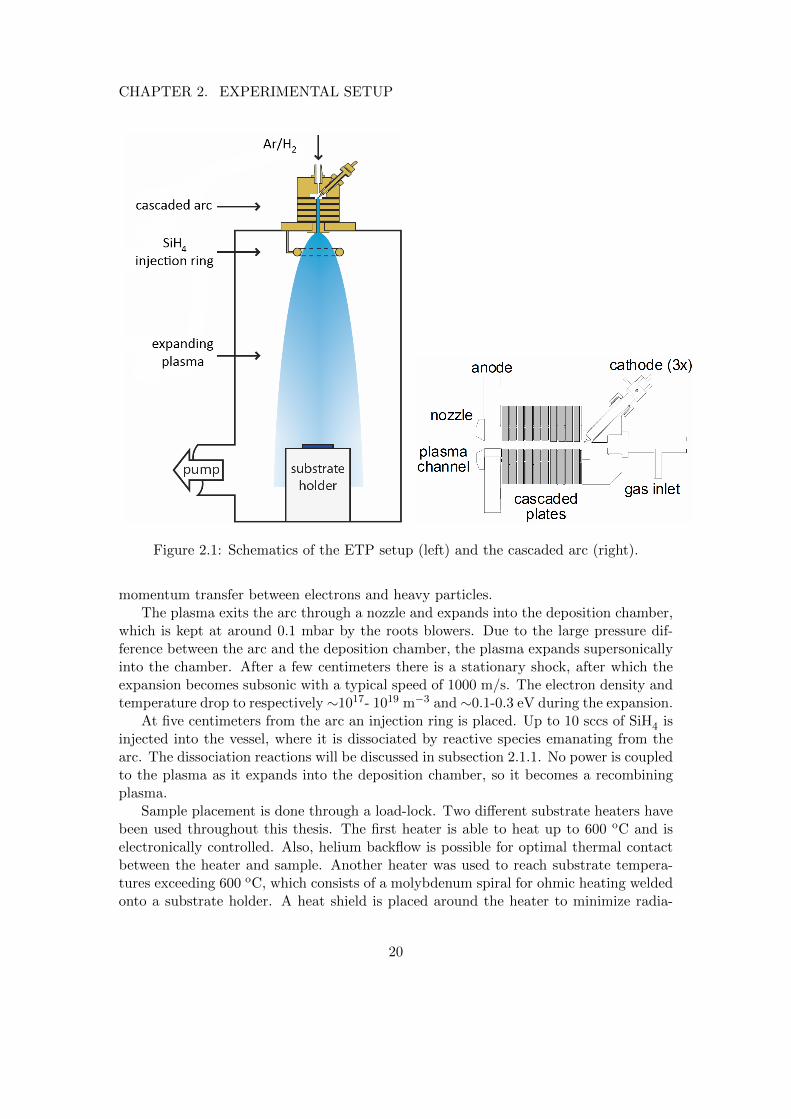
A schematic of the ETP setup is depicted in figure 2.1. The deposition chamberconsists of a cylindrical stainless steel vessel, 80 centimeters long and 50 centimeters indiameter. During depositions the chamber is evacuated by roots blowers, otherwise it ispumped down by a turbo pump, reaching a base pressure of 10−6 mbar.
The plasma is struck in a cascaded arc, which is a dc plasma source (see figure 2.1,right). The discharge is created by a potential drop between three cathode tips anda grounded anode plate, which are separated by alternating cascaded plates of copperand boronnitride. The source gas is argon, often mixed with hydrogen, which is flownthrough the plasma channel. During a typical deposition 15 A of current is driventhrough each cathode tip and, depending on the plasma composition, this results in apower dissipation of a few kilowatts, .
The plasma in the arc has an electron density of ∼1022 m−3 and both the electronand heavy particle temperature are ∼1 eV.[45] This thermal nature of the discharge isdue to the relatively high pressure of a few hundred mbar in the arc, leading to efficient
19
CHAPTER 2. EXPERIMENTAL SETUP
Figure 2.1: Schematics of the ETP setup (left) and the cascaded arc (right).
momentum transfer between electrons and heavy particles.The plasma exits the arc through a nozzle and expands into the deposition chamber,
which is kept at around 0.1 mbar by the roots blowers. Due to the large pressure dif-ference between the arc and the deposition chamber, the plasma expands supersonicallyinto the chamber. After a few centimeters there is a stationary shock, after which theexpansion becomes subsonic with a typical speed of 1000 m/s. The electron density andtemperature drop to respectively ∼1017- 1019 m−3 and ∼0.1-0.3 eV during the expansion.
At five centimeters from the arc an injection ring is placed. Up to 10 sccs of SiH4 isinjected into the vessel, where it is dissociated by reactive species emanating from thearc. The dissociation reactions will be discussed in subsection 2.1.1. No power is coupledto the plasma as it expands into the deposition chamber, so it becomes a recombiningplasma.
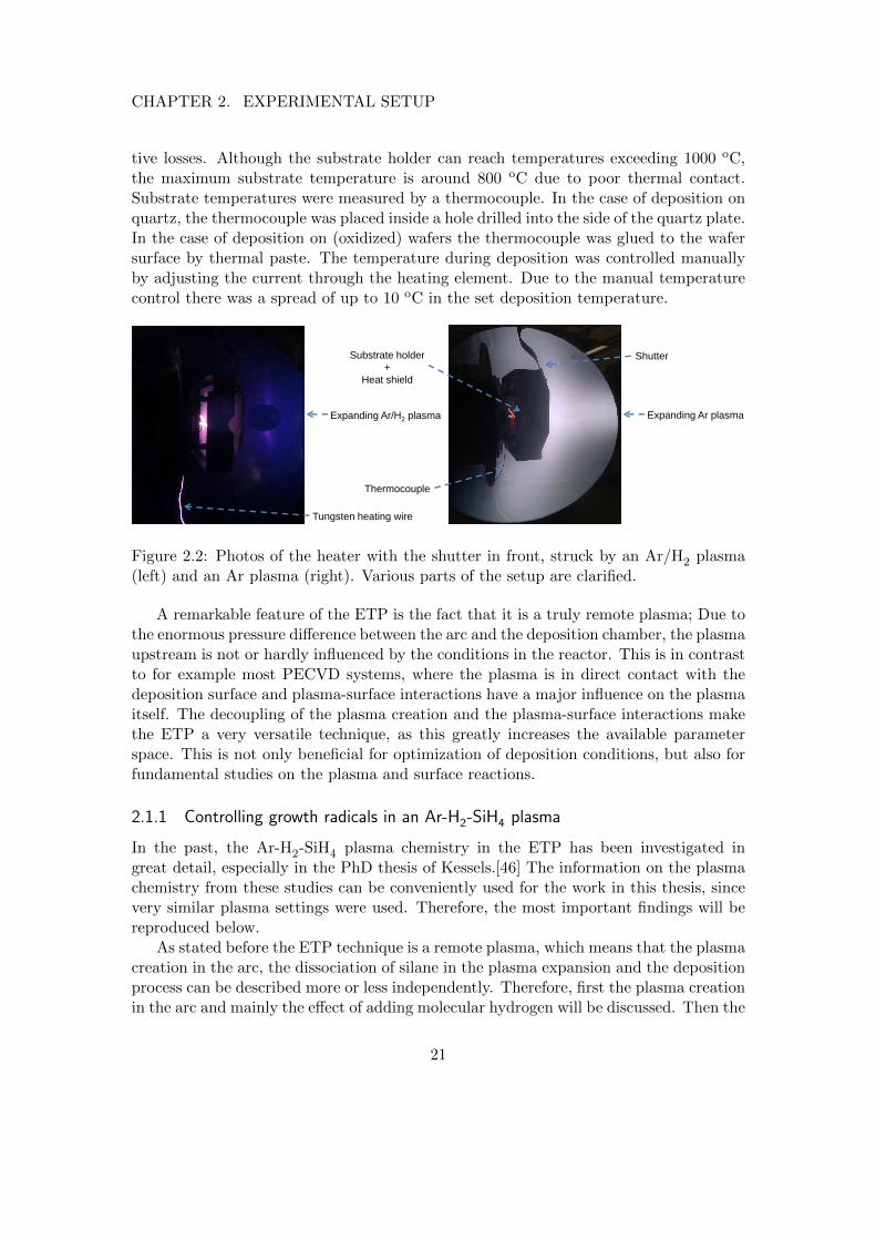
Sample placement is done through a load-lock. Two different substrate heaters havebeen used throughout this thesis. The first heater is able to heat up to 600 oC and iselectronically controlled. Also, helium backflow is possible for optimal thermal contactbetween the heater and sample. Another heater was used to reach substrate tempera-tures exceeding 600 oC, which consists of a molybdenum spiral for ohmic heating weldedonto a substrate holder. A heat shield is placed around the heater to minimize radia-
20
CHAPTER 2. EXPERIMENTAL SETUP
tive losses. Although the substrate holder can reach temperatures exceeding 1000 oC,the maximum substrate temperature is around 800 oC due to poor thermal contact.Substrate temperatures were measured by a thermocouple. In the case of deposition onquartz, the thermocouple was placed inside a hole drilled into the side of the quartz plate.In the case of deposition on (oxidized) wafers the thermocouple was glued to the wafersurface by thermal paste. The temperature during deposition was controlled manuallyby adjusting the current through the heating element. Due to the manual temperaturecontrol there was a spread of up to 10 oC in the set deposition temperature.
Expanding Ar/H2 plasma Expanding Ar plasma
Thermocouple
Substrate holder
+
Heat shield
Shutter
Tungsten heating wire
Figure 2.2: Photos of the heater with the shutter in front, struck by an Ar/H2 plasma(left) and an Ar plasma (right). Various parts of the setup are clarified.
A remarkable feature of the ETP is the fact that it is a truly remote plasma; Due tothe enormous pressure difference between the arc and the deposition chamber, the plasmaupstream is not or hardly influenced by the conditions in the reactor. This is in contrastto for example most PECVD systems, where the plasma is in direct contact with thedeposition surface and plasma-surface interactions have a major influence on the plasmaitself. The decoupling of the plasma creation and the plasma-surface interactions makethe ETP a very versatile technique, as this greatly increases the available parameterspace. This is not only beneficial for optimization of deposition conditions, but also forfundamental studies on the plasma and surface reactions.
2.1.1 Controlling growth radicals in an Ar-H2-SiH4 plasma
In the past, the Ar-H2-SiH4 plasma chemistry in the ETP has been investigated ingreat detail, especially in the PhD thesis of Kessels.[46] The information on the plasmachemistry from these studies can be conveniently used for the work in this thesis, sincevery similar plasma settings were used. Therefore, the most important findings will bereproduced below.
As stated before the ETP technique is a remote plasma, which means that the plasmacreation in the arc, the dissociation of silane in the plasma expansion and the depositionprocess can be described more or less independently. Therefore, first the plasma creationin the arc and mainly the effect of adding molecular hydrogen will be discussed. Then the
21
CHAPTER 2. EXPERIMENTAL SETUP
dissociation mechanism of silane in the deposition chamber due to the reactive speciesemanating from the arc is treated for various hydrogen flows. Finally the effect of plasmaparameters on the growth flux of the various silyl radicals will be made clear.
The discharge is created in the arc, through which (for most experiments) 55 sccsof argon is flown. If no hydrogen is added, the arc is a source of argon ions which areproduced in the breakdown. At the typical setting of 45 A the ion fluence from the arcis about 3 sccs, corresponding to an electron/ion density of ∼1019 m−3 at a position of 6centimeter from the arc outlet. The electron temperature at this position is around 0.3eV. The addition of hydrogen to the flow drastically changes the reactive species comingfrom the arc. Adding hydrogen changes the dominant specie from Ar+ to ArH+ for lowH2 flows and to H for high H2 flows of up to 10 sccs. More importantly, the molecularhydrogen leads to a strong reduction in the electron temperature and the ion flow fromthe arc, which drop to respectively ∼0.15 eV and 0.08 sccs for a H2 flow of 10 sccs. Also,the flux of atomic hydrogen greatly exceeds the ion flux, effectively rendering the arc asource of reactive H instead of an ion source.
The dissociation pathway of silane greatly depends on the type of reactive speciesemanating from the arc, and thus on the hydrogen flow. In the thesis of Kessels, areaction scheme for the dissociation process is presented for the two limiting cases of alow H2 flow (. 2 sccs) and high H2 flow (& 5 sccs).
In the case of no or low H2 flow, the main reactive species from the arc is Ar+,which is accompanied by a high electron density. The first step in silane dissociation isdissociative charge transfer from Ar+ to SiH4.
Ar+ + SiH4 → Ar + SiH+n ..(n ≤ 3) (2.1)
This reaction is followed by dissociative recombination with electrons, due to thehigh electron density at this condition.
SiH+n + e→ SiHm + ..(m ≤ 2) (2.2)
These lower radicals are very reactive with SiH4 and can therefore create polysilanesby sequential addition of silane molecules, especially at higher SiH4 partial pressures.
SiHm + SiH4 → Si2Hp + ..etc (2.3)
The electron density in the expansion is reduced through reaction 2.2. When the elec-tron to silane density ratio becomes .10−3 the dissociative recombination in reaction 2.2is no longer dominant and ion-molecule polymerization reactions lead to the formationof cationic clusters with up to 10 Si atoms, as determined by mass spectrometry.[47]
SipH+q + SiH4 → Sip+1H
+r + ..etc (2.4)
For H2 flows & 5 sccs the arc becomes a source of mainly H atoms, rendering thehydrogen abstraction of silane the most prominent reaction.
SiH4 + H→ SiH3 + H2 (2.5)
22
CHAPTER 2. EXPERIMENTAL SETUP
There is also still a small flux of hydrogen ions coming from the arc, which undergodissociative charge transfer reactions with silane
H+ + SiH4 → H + SiH+n ..(n ≤ 3) (2.6)
Because of the low electron density at high H2 flow, the main reaction of these silylions is the polymerization reaction in equation 2.4.
The precise deposition conditions used in this thesis are mentioned in the correspond-ing chapters.
2.2 Characterization techniques
2.2.1 Fourier Transform Infrared Spectroscopy
FTIR is an analysis technique that provides information on the chemical bonding in amaterial. It is based on the absorption of infrared light by a material, which leads toexcitation of vibrational modes (or even rotational modes for gas-phase spectroscopy)specific to certain bond configurations.
Since the various vibrational modes each have a specific eigenenergy, the part of theinfrared light passing a sample that matches that eigenenergy is strongly absorbed andappears as an absorption band in a FTIR spectrum. However, the bond must have anet dipole moment for light absorption to occur, since otherwise the transition dipolemoment is zero. For this reason the linear symmetric molecule N2 does not absorb IRlight, whereas CO2 does show strong absorption features.
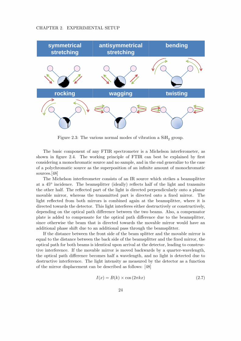
The vibrational energy levels of film species all belong to a specific normal modeof vibration. In the case of for example a SiH2 group, there are six normal modes ofvibration, which are schematically drawn in figure 2.3. Note that for each normal modein the figure, the two green arrows represent the movement direction during the first halfof the oscillation period, whereas the red arrows represent the movement in the secondhalf of the period.
In the figure the atoms are drawn as free-standing, which makes their normal modeswell-defined. However, in reality the vibrational modes are influenced by their bondingenvironment, which can both shift the resonance energy and lead to absorption bandbroadening. This will be made clear by a few examples. An FTIR spectrum of gas-phasespecies shows very sharp peaks, since the gas-phase molecules have little interaction andtherefore the vibrational modes are well-defined. Peaks of species adsorbed on a surfacedo show broadening, since there will be a distribution of their vibrational energy levelsdue to influences of for example the local surface geometry and the nature of surfacespecies that are adsorbed on neighbouring surface sites. In bulk species, the peak shiftand broadening effects are even more pronounced. For example, the energy of the bulkSi-H stretching mode is dependent on whether the H-atom is located at a vacancy orat the surface of a nanosized void, as will be elucidated below. So an FTIR spectrumcan not only provide information on the kind of bonds in the material, but also on themicrostructure in which these bonds reside.
23
CHAPTER 2. EXPERIMENTAL SETUP
symmetrical
stretching
antisymmetrical
stretching
bending
rocking wagging twisting
Figure 2.3: The various normal modes of vibration a SiH2 group.
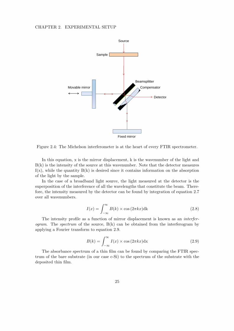
The basic component of any FTIR spectrometer is a Michelson interferometer, asshown in figure 2.4. The working principle of FTIR can best be explained by firstconsidering a monochromatic source and no sample, and in the end generalize to the caseof a polychromatic source as the superposition of an infinite amount of monochromaticsources.[48]
The Michelson interferometer consists of an IR source which strikes a beamsplitterat a 45o incidence. The beamsplitter (ideally) reflects half of the light and transmitsthe other half. The reflected part of the light is directed perpendicularly onto a planarmovable mirror, whereas the transmitted part is directed onto a fixed mirror. Thelight reflected from both mirrors is combined again at the beamsplitter, where it isdirected towards the detector. This light interferes either destructively or constructively,depending on the optical path difference between the two beams. Also, a compensatorplate is added to compensate for the optical path difference due to the beamsplitter,since otherwise the beam that is directed towards the movable mirror would have anadditional phase shift due to an additional pass through the beamsplitter.
If the distance between the front side of the beam splitter and the movable mirror isequal to the distance between the back side of the beamsplitter and the fixed mirror, theoptical path for both beams is identical upon arrival at the detector, leading to construc-tive interference. If the movable mirror is moved backwards by a quarter-wavelength,the optical path difference becomes half a wavelength, and no light is detected due todestructive interference. The light intensity as measured by the detector as a functionof the mirror displacement can be described as follows: [48]
I(x) = B(k)× cos (2πkx) (2.7)
24
CHAPTER 2. EXPERIMENTAL SETUP
Fixed mirror
Movable mirror
Source
Sample
Beamsplitter
Compensator
Detector
Figure 2.4: The Michelson interferometer is at the heart of every FTIR spectrometer.
In this equation, x is the mirror displacement, k is the wavenumber of the light andB(k) is the intensity of the source at this wavenumber. Note that the detector measuresI(x), while the quantity B(k) is desired since it contains information on the absorptionof the light by the sample.
In the case of a broadband light source, the light measured at the detector is thesuperposition of the interference of all the wavelengths that constitute the beam. There-fore, the intensity measured by the detector can be found by integration of equation 2.7over all wavenumbers.
I(x) =
∫ ∞−∞
B(k)× cos (2πkx)dk (2.8)
The intensity profile as a function of mirror displacement is known as an interfer-ogram. The spectrum of the source, B(k) can be obtained from the interferogram byapplying a Fourier transform to equation 2.9.
B(k) =
∫ ∞−∞
I(x)× cos (2πkx)dx (2.9)
The absorbance spectrum of a thin film can be found by comparing the FTIR spec-trum of the bare substrate (in our case c-Si) to the spectrum of the substrate with thedeposited thin film.
25
CHAPTER 2. EXPERIMENTAL SETUP
In this subsection, the most important silicon-hydride and oxidation modes that arisein the spectra of amorphous, microcrystalline and polycrystalline silicon thin films arediscussed.
In a-Si:H hydrogen can reside in either vacancies or on the surface of nanosized voids.It has been shown by Smets et al. that the hydrogen stretching mode in a-Si:H is differentfor these two configurations.[49] Hydrogen in a vacancy has a so-called low stretchingmode (LSM) around 1980-2010 cm−1, while hydrogen on the surface of nanosized voidshas a high stretching mode (HSM), around 2070-2100 cm−1. The hydrogen distributionin a-Si:H (or mc-Si:H) can thus be determined from the LSM and HSM peaks in an FTIRspectrum. This is quantified by the microstructure parameter R∗, which is defined asthe HSM integrated absorbance over the total hydrogen stretching mode absorbance:
R∗ =AHSM
ALSM +AHSM(2.10)
Therefore, a high R∗ represents a high fraction of voids in the film.In the case of µc-Si:H and poly-Si:H, hydrogen bonded to crystal grain surface gives
rise to three additional narrow high stretching modes (NHSM) at 2083, 2103, and 2137cm−1, which correspond to mono-, di- and trihydride configurations, respectively.[50, 51]The presence of NHSM modes typically indicates that the crystal grains are bound byvoids instead of amorphous silicon, rendering the film prone to oxidation.[51, 52]
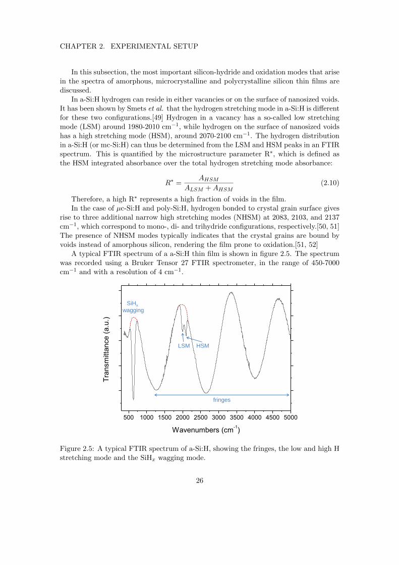
A typical FTIR spectrum of a a-Si:H thin film is shown in figure 2.5. The spectrumwas recorded using a Bruker Tensor 27 FTIR spectrometer, in the range of 450-7000cm−1 and with a resolution of 4 cm−1.
500 1000 1500 2000 2500 3000 3500 4000 4500 5000
Tra
nsm
itta
nce (
a.u
.)
Wavenumbers (cm-1)
fringes
SiHx
wagging
LSM HSM
Figure 2.5: A typical FTIR spectrum of a-Si:H, showing the fringes, the low and high Hstretching mode and the SiHx wagging mode.
26
CHAPTER 2. EXPERIMENTAL SETUP
The most prominent feature in the spectrum are the fringes, which arise due tointernal reflections of the beam in the a-Si:H thin film. These fringes can be used todetermine the thickness and refractive index of the film, using a simple three-layer modelas described in reference [53]. The LSM and HSM modes show up as absorption bands,as well as the SiHx wagging modes around 600-680 cm−1.[52] Additionally, the totalhydrogen content of the film can be determined by integration of the wagging mode, asdescribed in reference [54]. This specific mode is used, since every hydrogen bonded inthe bulk contributes to this mode.
Oxidation of a silicon film can be seen in an FTIR spectrum by the presence of a Si-O-Si antisymmetric stretching mode around 1050 cm−1 and by the shift of the hydrogenstretching mode to 2200-2250 cm−1 due to oxygen bonded to the Si-Si backbond. Inthe 700-900 cm−1 region, various oxidation peaks are convoluted, which are the Si-O-Sisymmetric stretching, O-Si-H deformation, Si-O stretching and O-H bending of SiOHmodes.[55, 56]
2.2.2 Raman Spectroscopy
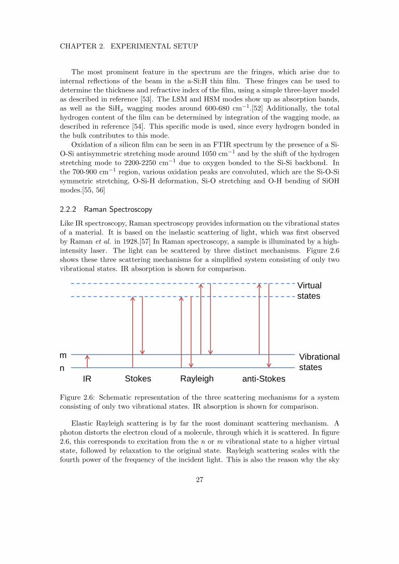
Like IR spectroscopy, Raman spectroscopy provides information on the vibrational statesof a material. It is based on the inelastic scattering of light, which was first observedby Raman et al. in 1928.[57] In Raman spectroscopy, a sample is illuminated by a high-intensity laser. The light can be scattered by three distinct mechanisms. Figure 2.6shows these three scattering mechanisms for a simplified system consisting of only twovibrational states. IR absorption is shown for comparison.
n
m
IR Stokes Rayleigh anti-Stokes
Virtual
states
Vibrational
states
Figure 2.6: Schematic representation of the three scattering mechanisms for a systemconsisting of only two vibrational states. IR absorption is shown for comparison.
Elastic Rayleigh scattering is by far the most dominant scattering mechanism. Aphoton distorts the electron cloud of a molecule, through which it is scattered. In figure2.6, this corresponds to excitation from the n or m vibrational state to a higher virtualstate, followed by relaxation to the original state. Rayleigh scattering scales with thefourth power of the frequency of the incident light. This is also the reason why the sky
27
CHAPTER 2. EXPERIMENTAL SETUP
is blue; The blue part of the solar spectrum is scattered more efficiently by molecules inthe atmosphere than the red part. Note that unlike (IR) absorption, there is no needfor the incident light to match a certain electronic transition for the scattering to occur.
Inelastic Stokes (or Raman) scattering is a far less efficient process, by a factor of∼ 106 − 108.[58] In Stokes scattering, nuclear motion is induced. The scattered photonhas an energy which is its energy prior to scattering minus the energy of the inducedvibrational motion. This shift in energy is the Stokes or Raman shift. In figure 2.6 this isvisualized as excitation from the lower energy state n to a virtual energy state, followedby relaxation to the higher energy level m.
Inelastic anti-Stokes scattering is very similar to Stokes scattering. Anti-Stokes scat-tering is the scattering of a photon from a molecule which is already vibrationally ex-cited. The molecule is demoted to a lower vibrational energy level, transferring thisenergy to the scattered photon. This also leads to a Raman shift, but towards a higherenergy. Since at room temperature most systems are typically dominantly in their vibra-tional ground-state, anti-Stokes scattering is even more inefficient than Stokes scattering.However, by comparing the intensity of Stokes and anti-Stokes shifts, information on thepopulation of the vibrational system, and thus its temperature, can be obtained.
One might wonder what the advantage of Raman is over for example FTIR, sinceboth techniques provide information on the vibrational states of a system. In fact thetechniques are complementary since a vibrational mode that is Raman-active is notnecessarily IR-active, and vice versa. This is due to different selection rules for bothprocesses. Whereas a bond must have a net dipole in order to be IR-active, it appearsthat a vibrational mode is only Raman-active if the electric field of an incident photoninduces a change in the polarizability tensor. Most antisymmetric modes change thenet dipole moment, whereas changes in the polarizability occur most frequently forsymmetric modes. Nonetheless, modes can certainly be both IR and Raman-active.Only for centrosymmetric systems a mode can not be both IR and Raman active, whichis known as the mutual exclusion rule.[58]
The discussion above described the Raman effect by molecular vibrations. In thecase of a solid, these vibrations are represented by phonon modes.
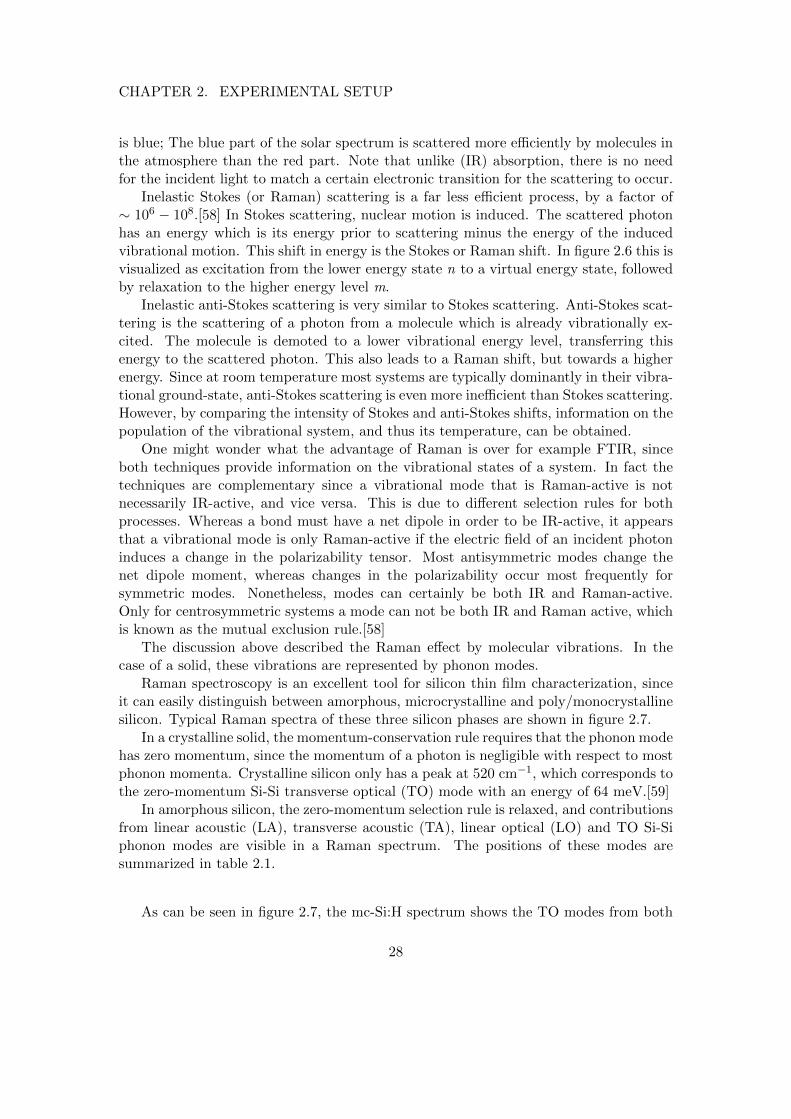
Raman spectroscopy is an excellent tool for silicon thin film characterization, sinceit can easily distinguish between amorphous, microcrystalline and poly/monocrystallinesilicon. Typical Raman spectra of these three silicon phases are shown in figure 2.7.
In a crystalline solid, the momentum-conservation rule requires that the phonon modehas zero momentum, since the momentum of a photon is negligible with respect to mostphonon momenta. Crystalline silicon only has a peak at 520 cm−1, which corresponds tothe zero-momentum Si-Si transverse optical (TO) mode with an energy of 64 meV.[59]
In amorphous silicon, the zero-momentum selection rule is relaxed, and contributionsfrom linear acoustic (LA), transverse acoustic (TA), linear optical (LO) and TO Si-Siphonon modes are visible in a Raman spectrum. The positions of these modes aresummarized in table 2.1.
As can be seen in figure 2.7, the mc-Si:H spectrum shows the TO modes from both
28
CHAPTER 2. EXPERIMENTAL SETUP
1 0 0 1 5 0 2 0 0 2 5 0 3 0 0 3 5 0 4 0 0 4 5 0 5 0 0 5 5 0
Norm
alized
Inten
sity (a
.u.)
R a m a n s h i f t ( c m - 1 )
a - S i : H µc - S i : H p o l y - S i
Figure 2.7: Typical normalized Raman spectra of a-Si:H, µc-Si:H and poly-Si.
Material phase Phonon mode Peak position (cm−1)
c-Si TO 520a-Si:H TO 475 ± 10
LO 380 ± 10TA 300 ± 10LA 140 ± 5
Table 2.1: The various Raman-active phonon modes in c-Si and a-Si:H [59, 60]
a-Si:H and c-Si. As proposed by Tsu et al., the crystalline fraction Xc can be determinedfrom the integrated areas of these two TO modes.[61]
Xc =Ic
Ic + γIa(2.11)
In this, Ic and Ia denote the integrated areas of the crystalline and amorphous TOmodes, respectively. The factor γ accounts for the difference in Raman scattering crosssection between amorphous and crystalline silicon. Most authors take γ to be around0.8 for mc-Si:H. However, it appears that the Raman cross section for crystallites inmc-Si:H is strongly dependent on the crystallite size. Bustarret et al. have found anempirical formula for γ as a function of crystallite size d (d in nanometers).[62]
γ(d) = 0.1 + exp (−d/25) (2.12)
Therefore, care must be taken in the determination of Xc, especially for films with
29
CHAPTER 2. EXPERIMENTAL SETUP
large crystallites where the deviation from the commonly-used γ value of 0.8 can besignificant.
Raman spectra were taken with a Renishaw Invia Raman spectroscope. The laserexcitation wavelength was 514 nm. Scans were made in the 20-1000 cm−1 Raman shiftregion with a resolution of 1.6 cm−1. The laser power was set to 5 mW and the acquisitiontime was fixed at ten seconds.
2.2.3 Spectroscopic ellipsometry
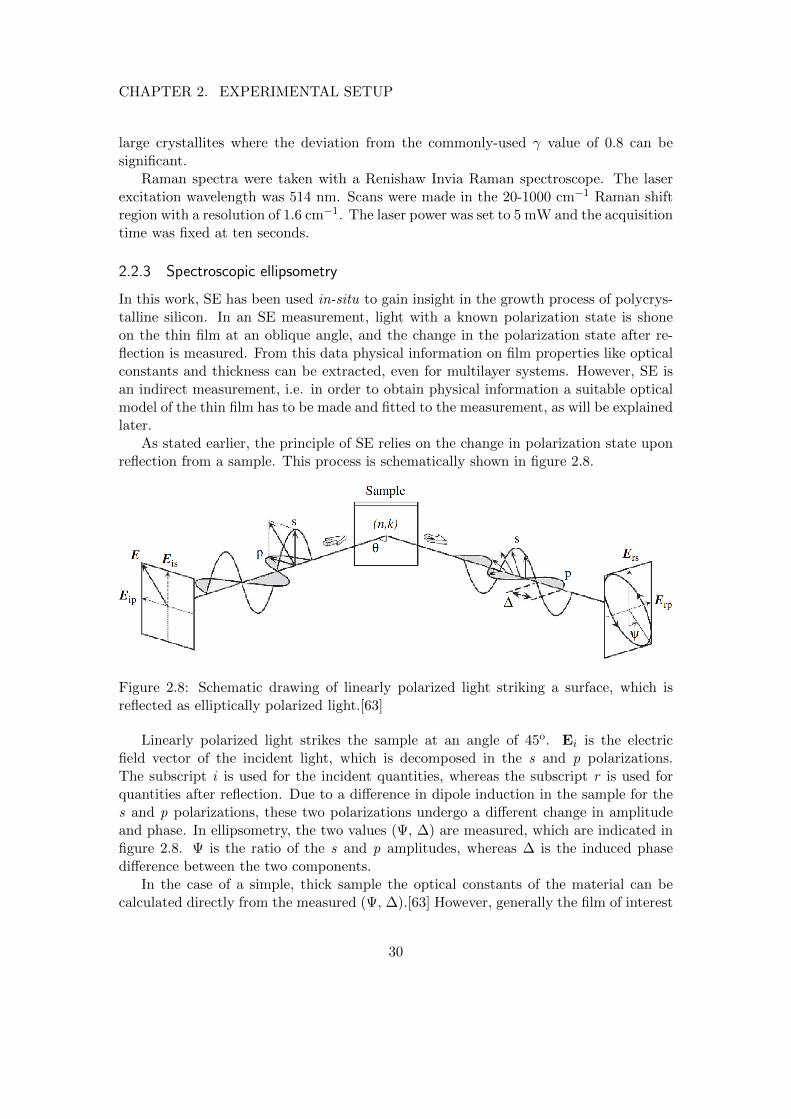
In this work, SE has been used in-situ to gain insight in the growth process of polycrys-talline silicon. In an SE measurement, light with a known polarization state is shoneon the thin film at an oblique angle, and the change in the polarization state after re-flection is measured. From this data physical information on film properties like opticalconstants and thickness can be extracted, even for multilayer systems. However, SE isan indirect measurement, i.e. in order to obtain physical information a suitable opticalmodel of the thin film has to be made and fitted to the measurement, as will be explainedlater.
As stated earlier, the principle of SE relies on the change in polarization state uponreflection from a sample. This process is schematically shown in figure 2.8.
Figure 2.8: Schematic drawing of linearly polarized light striking a surface, which isreflected as elliptically polarized light.[63]
Linearly polarized light strikes the sample at an angle of 45o. Ei is the electricfield vector of the incident light, which is decomposed in the s and p polarizations.The subscript i is used for the incident quantities, whereas the subscript r is used forquantities after reflection. Due to a difference in dipole induction in the sample for thes and p polarizations, these two polarizations undergo a different change in amplitudeand phase. In ellipsometry, the two values (Ψ, ∆) are measured, which are indicated infigure 2.8. Ψ is the ratio of the s and p amplitudes, whereas ∆ is the induced phasedifference between the two components.
In the case of a simple, thick sample the optical constants of the material can becalculated directly from the measured (Ψ, ∆).[63] However, generally the film of interest
30
CHAPTER 2. EXPERIMENTAL SETUP
can be comprised out of different layers, with even for example thin oxide layers inbetween. The various reflections from these interfaces make the interpretation of (Ψ, ∆)much less trivial. Other complicating factors are for example surface roughness, voidincorporation in the film or even mixed-phase films.
Fortunately, modeling of the thin-film of interest makes it possible to extract aplethora of physical film properties from the spectroscopically measured (Ψ, ∆). Typ-ically, modeling of a multilayer system is done using a software package (in our caseCompleteEASE) as follows. A model comprised of a stack of layers with correspondinglayer thicknesses is defined in the software, which is thought to be representative of thephysical system. Since the dielectric functions of the materials are known, the expected(Ψ, ∆) response of this model can be calculated. The result is compared to the measured(Ψ, ∆), and model parameters (e.g. layer thicknesses, void content, roughness and sub-strate temperature) are varied iteratively to fit the calculated (Ψ, ∆) to the measured(Ψ, ∆).
If the dielectric function of a layer is not known, this dielectric function can also beobtained from the spectroscopically measured (Ψ, ∆) by fitting. The dielectric functionof the layer is in this case represented by a B-spline, which is forced to be Kramers-Kronig consistent. In this work, a B-spline is used to discriminate between amorphousand crystalline silicon growth, as will be elaborated in chapter 4.
For our in-situ measurements, a Woollam rotating compensator ellipsometer wasused. Scan times were set to 1 second, as this was found to be a good compromisebetween temporal resolution and signal-to-noise ratio. The SE source and detector weremounted to two viewports of the chamber, which have an 75o angle with the substrate.Prior to deposition, the substrate (mostly a Si (100) wafer with 450 nm of oxide) wasbrought to the deposition temperature and was scanned for a longer time. This allowedfor a precise determination of the starting layer. The film model used for modeling ispresented in chapter 4.
2.2.4 X-ray Diffraction
XRD is an analysis technique that can provide information on the crystal structure of amaterial. Its working principle is based on destructive and constructive interference ofcoherent X-ray radiation that is diffracted on a periodic structure, like a crystal of atoms.The working principle can most easily be demonstrated by considering the simple caseof diffraction from a two dimensional square lattice with spacing d, as shown in figure2.9.
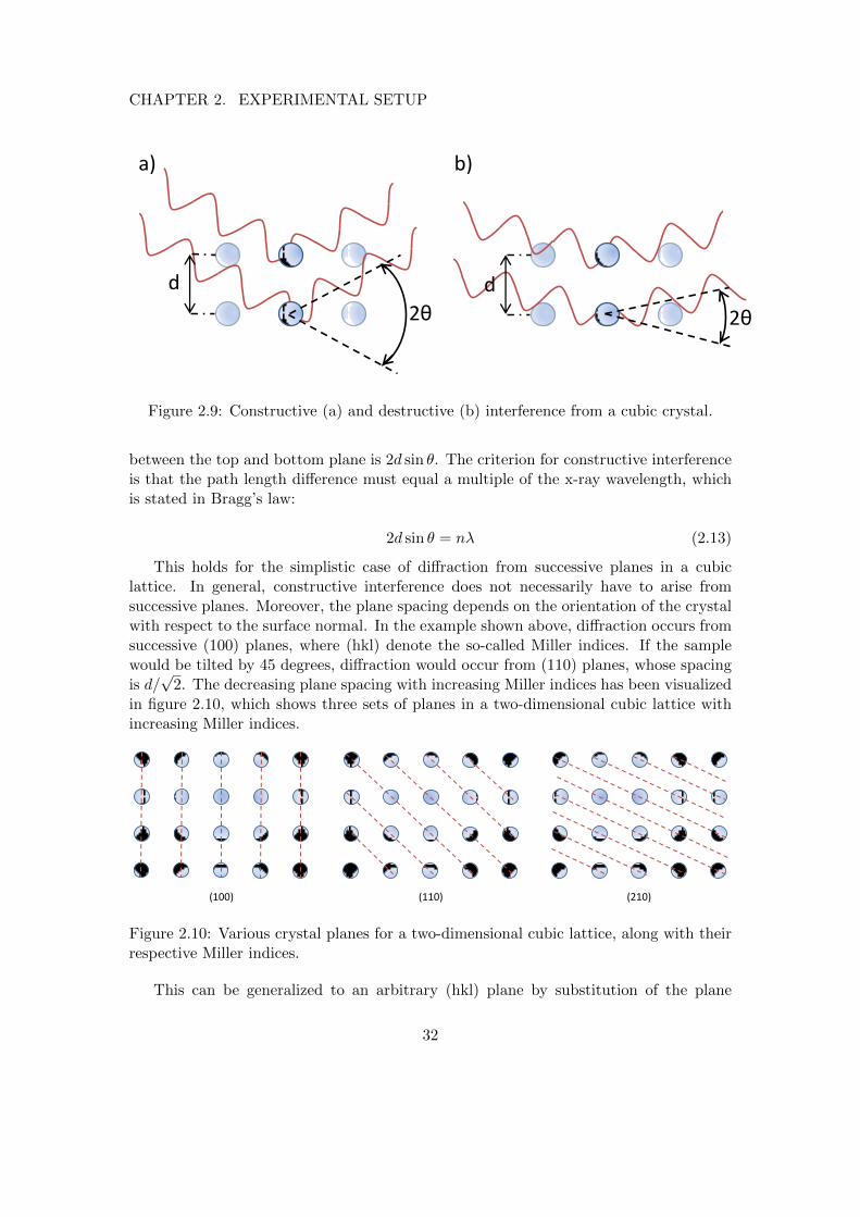
Two cases are shown: Constructive (a) and destructive (b) interference. A coherentX-ray beam is incident on the crystal with an angle θ with respect to the surface. Thebeam is diffracted isotropically by the periodic atoms. Depending on the angle θ, photonsfrom successive crystal planes will either interfere constructively or destructively. In thecase of figure 2.9a, the path length difference between the top and bottom plane is exactlyone wavelength, thus leading to constructive interference. In 2.9b, the path lengthdifference is only half a wavelength, so the two photons cancel out due to destructiveinterference. With some basic geometry, it can be shown that the path length difference
31
CHAPTER 2. EXPERIMENTAL SETUP
d
2θ
a)
d
2θ
b)
Figure 2.9: Constructive (a) and destructive (b) interference from a cubic crystal.
between the top and bottom plane is 2d sin θ. The criterion for constructive interferenceis that the path length difference must equal a multiple of the x-ray wavelength, whichis stated in Bragg’s law:
2d sin θ = nλ (2.13)
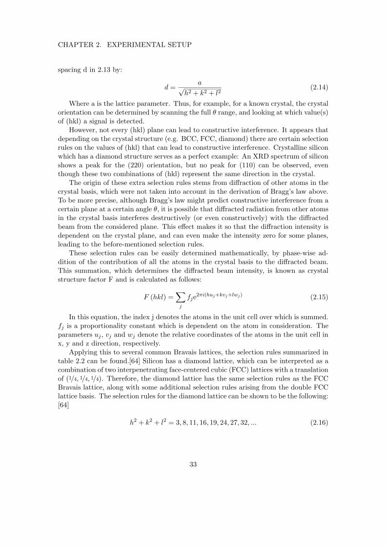
This holds for the simplistic case of diffraction from successive planes in a cubiclattice. In general, constructive interference does not necessarily have to arise fromsuccessive planes. Moreover, the plane spacing depends on the orientation of the crystalwith respect to the surface normal. In the example shown above, diffraction occurs fromsuccessive (100) planes, where (hkl) denote the so-called Miller indices. If the samplewould be tilted by 45 degrees, diffraction would occur from (110) planes, whose spacingis d/√
2. The decreasing plane spacing with increasing Miller indices has been visualizedin figure 2.10, which shows three sets of planes in a two-dimensional cubic lattice withincreasing Miller indices.
(100) (110) (210)
Figure 2.10: Various crystal planes for a two-dimensional cubic lattice, along with theirrespective Miller indices.
This can be generalized to an arbitrary (hkl) plane by substitution of the plane
32
CHAPTER 2. EXPERIMENTAL SETUP
spacing d in 2.13 by:
d =a√
h2 + k2 + l2(2.14)
Where a is the lattice parameter. Thus, for example, for a known crystal, the crystalorientation can be determined by scanning the full θ range, and looking at which value(s)of (hkl) a signal is detected.
However, not every (hkl) plane can lead to constructive interference. It appears thatdepending on the crystal structure (e.g. BCC, FCC, diamond) there are certain selectionrules on the values of (hkl) that can lead to constructive interference. Crystalline siliconwhich has a diamond structure serves as a perfect example: An XRD spectrum of siliconshows a peak for the (220) orientation, but no peak for (110) can be observed, eventhough these two combinations of (hkl) represent the same direction in the crystal.
The origin of these extra selection rules stems from diffraction of other atoms in thecrystal basis, which were not taken into account in the derivation of Bragg’s law above.To be more precise, although Bragg’s law might predict constructive interference from acertain plane at a certain angle θ, it is possible that diffracted radiation from other atomsin the crystal basis interferes destructively (or even constructively) with the diffractedbeam from the considered plane. This effect makes it so that the diffraction intensity isdependent on the crystal plane, and can even make the intensity zero for some planes,leading to the before-mentioned selection rules.
These selection rules can be easily determined mathematically, by phase-wise ad-dition of the contribution of all the atoms in the crystal basis to the diffracted beam.This summation, which determines the diffracted beam intensity, is known as crystalstructure factor F and is calculated as follows:
F (hkl) =∑j
fje2πi(huj+kvj+lwj) (2.15)
In this equation, the index j denotes the atoms in the unit cell over which is summed.fj is a proportionality constant which is dependent on the atom in consideration. Theparameters uj , vj and wj denote the relative coordinates of the atoms in the unit cell inx, y and z direction, respectively.
Applying this to several common Bravais lattices, the selection rules summarized intable 2.2 can be found.[64] Silicon has a diamond lattice, which can be interpreted as acombination of two interpenetrating face-centered cubic (FCC) lattices with a translationof (1/4, 1/4, 1/4). Therefore, the diamond lattice has the same selection rules as the FCCBravais lattice, along with some additional selection rules arising from the double FCClattice basis. The selection rules for the diamond lattice can be shown to be the following:[64]
h2 + k2 + l2 = 3, 8, 11, 16, 19, 24, 27, 32, ... (2.16)
33
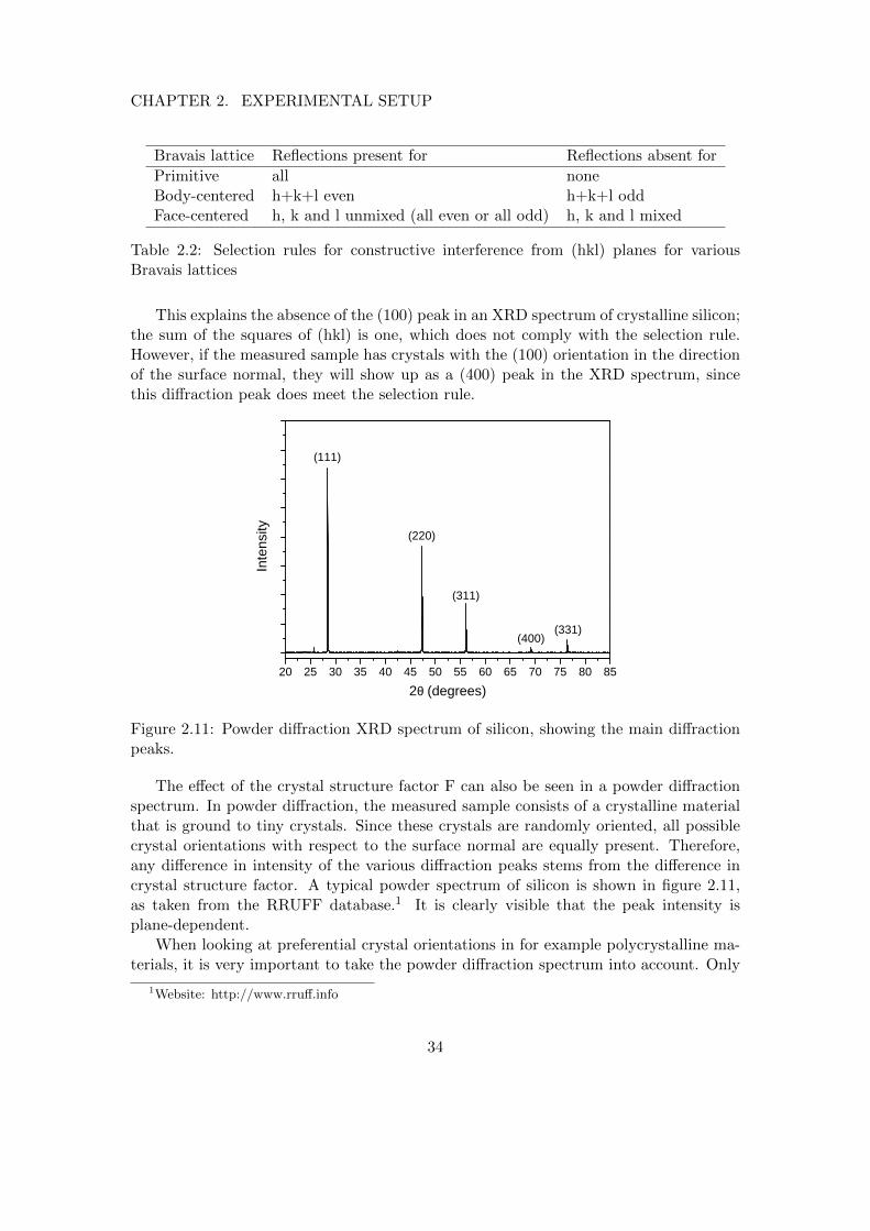
CHAPTER 2. EXPERIMENTAL SETUP
Bravais lattice Reflections present for Reflections absent for
Primitive all noneBody-centered h+k+l even h+k+l oddFace-centered h, k and l unmixed (all even or all odd) h, k and l mixed
Table 2.2: Selection rules for constructive interference from (hkl) planes for variousBravais lattices
This explains the absence of the (100) peak in an XRD spectrum of crystalline silicon;the sum of the squares of (hkl) is one, which does not comply with the selection rule.However, if the measured sample has crystals with the (100) orientation in the directionof the surface normal, they will show up as a (400) peak in the XRD spectrum, sincethis diffraction peak does meet the selection rule.
2 0 2 5 3 0 3 5 4 0 4 5 5 0 5 5 6 0 6 5 7 0 7 5 8 0 8 5
( 3 3 1 )( 4 0 0 )
( 3 1 1 )
( 2 2 0 )
Inten
sity
2 θ ( d e g r e e s )
( 1 1 1 )
Figure 2.11: Powder diffraction XRD spectrum of silicon, showing the main diffractionpeaks.
The effect of the crystal structure factor F can also be seen in a powder diffractionspectrum. In powder diffraction, the measured sample consists of a crystalline materialthat is ground to tiny crystals. Since these crystals are randomly oriented, all possiblecrystal orientations with respect to the surface normal are equally present. Therefore,any difference in intensity of the various diffraction peaks stems from the difference incrystal structure factor. A typical powder spectrum of silicon is shown in figure 2.11,as taken from the RRUFF database.1 It is clearly visible that the peak intensity isplane-dependent.
When looking at preferential crystal orientations in for example polycrystalline ma-terials, it is very important to take the powder diffraction spectrum into account. Only
1Website: http://www.rruff.info
34
CHAPTER 2. EXPERIMENTAL SETUP
after dividing the peaks in an XRD spectrum of a polycrystalline material by their re-spective powder diffraction peak heights, it is possible to reveal a preferential orientation;In the case of a randomly oriented polycrystalline film, all the peaks will have the sameheight after division. If a certain crystal orientation prevails preferentially, it will showup as the highest peak after division.
As a final note on XRD, it is also possible to deduce information on crystallite sizefrom a spectrum. As the crystallite size decreases, the width of the diffraction peakincreases. The reason for this can be made clear using a very simple argument andby looking at two limiting cases: Diffraction from only two successive planes, like infigure 2.9, and the case of diffraction from an infinite crystal. When diffraction occursfrom only two successive planes, there will still be some constructive interference whenslightly deviating from the Bragg angle. To be more precise, the diffracted beam intensitywill only drop to zero when going from the Bragg angle to the angle for destructiveinterference, so from (a) to (b) in figure 2.9. Therefore, the diffraction peak in an XRDspectrum would be very broad in this case. On the other hand, in the case of an infinitecrystal there will only be a diffraction peak exactly at the Bragg angle, and consequentlythe diffraction peak is a Dirac delta peak (ignoring instrumental broadening). To seewhy, consider the case of diffraction from an infinite crystal, at such an angle that thediffracted beams from the first two planes are out of phase by for example 1/10 of thewavelength. If there were only two planes, there would still be constructive interference.However, diffraction from the fifth plane will have a 1/2 wavelength difference, leadingexactly to destructive interference with the beam diffracted from the first plane. For aninfinite crystal, this will hold for any wavelength difference between successive planes,since there will always be diffraction from a plane that exactly cancels with diffractionfrom another plane. The only exception is diffraction at the Bragg angle at whichdiffraction from all planes is exactly in phase, which explains the Dirac delta peak foran infinite crystal.
The average crystallite size can be estimated from an XRD spectrum by applyingScherrer’s formula:
τ =Kλ
β cos θ(2.17)
In this equation, τ is the average crystallite size, λ the wavelength of the used x-ray(Cu K-α), β the full width at half maximum of the diffraction peak, and θ the diffractionangle. K is a dimensionless constant, known as the shape factor. It is dependent on theshape of the crystallite, and is usually taken as 0.89 for spherical crystals. Note that theScherrer formula provides a lower limit on the crystal size, since additional broadeningarises due to instrumental imperfections. An extensive review on the Scherrer formulaand the various shape factors can be found in reference [65].
XRD measurements have been performed on a Panalytical X’pert Pro MRD. Sollerslits were placed on both the incident and diffracted side to reduce the influence ofscattered signals. A nickel filter was used to attenuate radiation of the copper X-raysource other than the K-α radiation. Scans were taken in the 20-60o 2θ range.
35
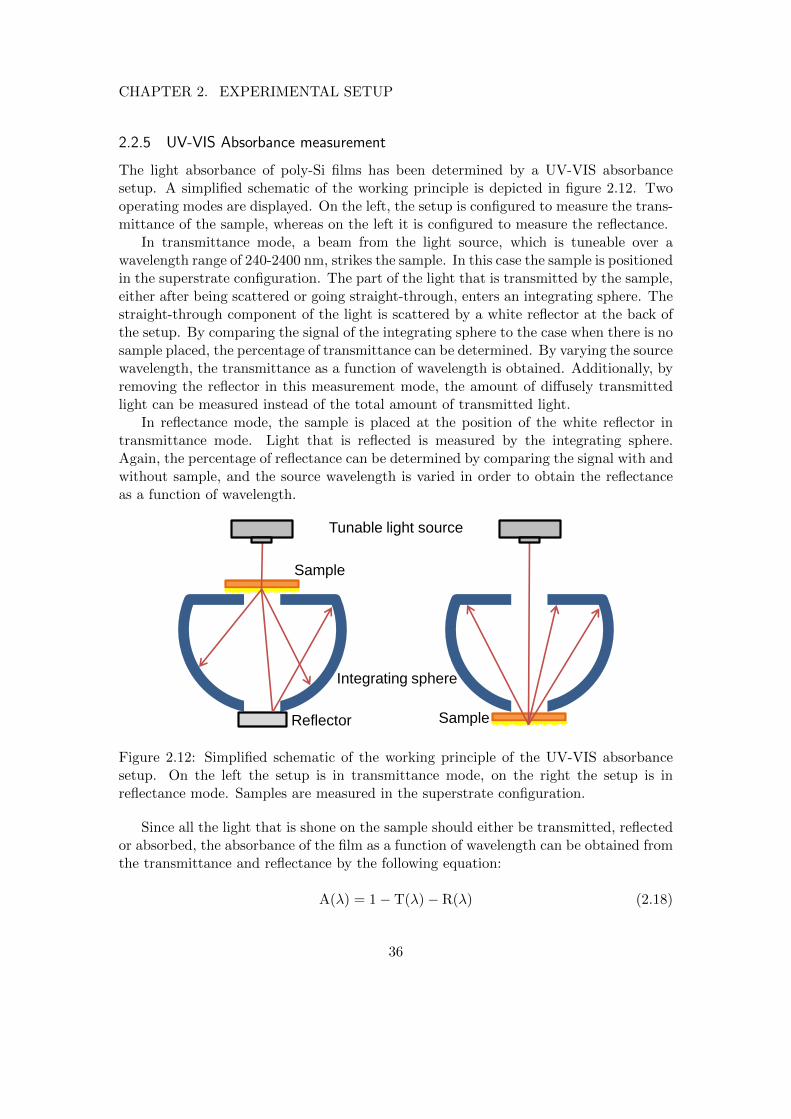
CHAPTER 2. EXPERIMENTAL SETUP
2.2.5 UV-VIS Absorbance measurement
The light absorbance of poly-Si films has been determined by a UV-VIS absorbancesetup. A simplified schematic of the working principle is depicted in figure 2.12. Twooperating modes are displayed. On the left, the setup is configured to measure the trans-mittance of the sample, whereas on the left it is configured to measure the reflectance.
In transmittance mode, a beam from the light source, which is tuneable over awavelength range of 240-2400 nm, strikes the sample. In this case the sample is positionedin the superstrate configuration. The part of the light that is transmitted by the sample,either after being scattered or going straight-through, enters an integrating sphere. Thestraight-through component of the light is scattered by a white reflector at the back ofthe setup. By comparing the signal of the integrating sphere to the case when there is nosample placed, the percentage of transmittance can be determined. By varying the sourcewavelength, the transmittance as a function of wavelength is obtained. Additionally, byremoving the reflector in this measurement mode, the amount of diffusely transmittedlight can be measured instead of the total amount of transmitted light.
In reflectance mode, the sample is placed at the position of the white reflector intransmittance mode. Light that is reflected is measured by the integrating sphere.Again, the percentage of reflectance can be determined by comparing the signal with andwithout sample, and the source wavelength is varied in order to obtain the reflectanceas a function of wavelength.
Integrating sphere
Reflector
Sample
Tunable light source
Sample
Figure 2.12: Simplified schematic of the working principle of the UV-VIS absorbancesetup. On the left the setup is in transmittance mode, on the right the setup is inreflectance mode. Samples are measured in the superstrate configuration.
Since all the light that is shone on the sample should either be transmitted, reflectedor absorbed, the absorbance of the film as a function of wavelength can be obtained fromthe transmittance and reflectance by the following equation:
A(λ) = 1− T(λ)− R(λ) (2.18)
36
CHAPTER 2. EXPERIMENTAL SETUP
In this equation, A, T and R are the film absorbance, transmittance and reflectance,respectively.
Measurements were performed with a Shimadzu UV-3600 spectrophotometer. Mea-surements were taken in the 450-1100 nm wavelength region. 450 nm was taken as thelower bound, since this was the cut-off wavelength of the used glass and quartz sub-strates. The upper bound of 1100 nm was taken since this approximately matches thebandgap of c-Si (1.12 eV).
37
Chapter 3
Towards polycrystalline silicon depositionby ETP-CVD
3.1 Introduction
In this chapter the feasibility of depositing poly-Si by an expanding thermal plasma isexplored. Although the expanding thermal plasma is a technique capable of depositingdevice-grade a-Si:H at high deposition rates, poly-Si deposition was never attempted byETP. As stated in the outline, the expanding thermal plasma may have some specificadvantages with respect conventional techniques such as a high deposition rate and theabsence of high-energy ion bombardment.
Two approaches to explore the feasibilty of poly-Si deposition have been followed.The first approach is a low-temperature route (<600 oC) in which the SiH4 in an Ar-H2-SiH4 plasma is pulsed to allow for low-temperature crystal growth. This approach isinspired by the LBL technique, where short depositions of a-Si:H are alternated by anatomic hydrogen treatment that leads to crystallization of the film.[34, 37] The effectof the hydrogen treatment on the film crystallinity in our system was investigated anda tentative explanation for the observed results is given. The reason for taking thepulsed-deposition approach was because for the ETP setup no experimental conditionfor poly-Si deposition at substrate temperatures <600 oC is known, despite the extensiveinvestigation of parameter space in the past.
The second approach is a high-temperature route (>600 oC). As mentioned before,this high deposition temperature has specific disadvantages like the incompatibility withinexpensive glass substrates, diffusion of impurities across films and the need for post-hydrogenation of the poly-Si for dangling bond passivation. Nonetheless, in order toachieve full crystal growth the high substrate temperature may be necessary to compen-sate for the lack of ion bombardment-enhanced surface diffusion in ETP at the substrate.For this approach, the role of growth radicals and temperature on the film properties isinvestigated.
38
CHAPTER 3. TOWARDS POLYCRYSTALLINE SILICON DEPOSITION BYETP-CVD
3.2 Pulsed deposition for low-temperature crystal growth
For the pulsed silane deposition experiments a fast-acting ALD valve was connected tothe silane line, which has an open shutter time of ten milliseconds and a variable ’offtime’. In order to see if this approach can enhance film crystallinity, the optimizeddeposition condition for µc-Si:H was taken as the starting point. In this condition, thearc current is set to 45 A and gas flows are set to 55 sccs of Ar, 30 sccs of H2 and 0.33sccs of SiH4. The substrate temperature was set at 250 oC or 580 oC. The depositiontemperatures and off-times used for depositions are summarized in table 3.1.
Temperature Off-time(oC) (s)
250 0250 0.67250 1250 1.2250 1.5250 2580 0580 10580 20
Table 3.1: Deposition temper-atures and off-times used forthe pulsed depositions.
For depositions at 250 oC, the ’off-time’ has beenvaried between zero (continuous deposition) and twoseconds. It has to be noted that although the ALDvalve only opens for ten milliseconds during a deposi-tion cycle, the chamber residence time is approximately1.2 s, as inferred from QMS measurements. Therefore,for off-times lower than 1.2 s, there is no effective sepa-ration between the deposition and hydrogen treatmentcycles and the deposition is more or less continuous.For these low off-times the deposition is effectively car-ried out at a higher hydrogen/silane dilution ratio, andtherefore a higher crystallinity is expected. Only foroff-times above the chamber residence time there is aneffective hydrogen treatment that can affect film prop-erties.
The Raman spectra for the various off-times areshown in figure 3.1(a). For these films, the total de-position time was kept constant at 400 seconds. Thecorresponding film crystallinity is displayed in figure3.1(b).
For off-times well below the chamber residence time an increase in film crystallinitywith respect to the continuous deposition is observed, as expected. For off-times abovethe chamber residence time, the crystalline fraction decreases rapidly, as seen by thedecrease in the 520 cm−1 TO peak of c-Si, indicating that the hydrogen treatmentinduces an amorphization of the film.
FTIR spectroscopy indicates a microstructural change for increasing off-time, asshown in figure 3.2. In the case of continuous deposition the film is dominated byNHSM (hydrogen bonded on crystal grain surfaces) and hardly any LSM is detected(i.e. low density of hydrogen in vacancies). The hydrogen treatment increases boththe LSM and HSM contribution, while decreasing the NHSM peaks. It is tempting tosuggest that because of the observed decrease in NHSM the pulsed deposition results infilms where the grain boundaries are better passivated by amorphous tissue. However,care must be taken since also the crystalline content is decreased when increasing theoff-time. The presence of the convoluted oxidation peaks in the 800 - 1200 cm−1 region
39
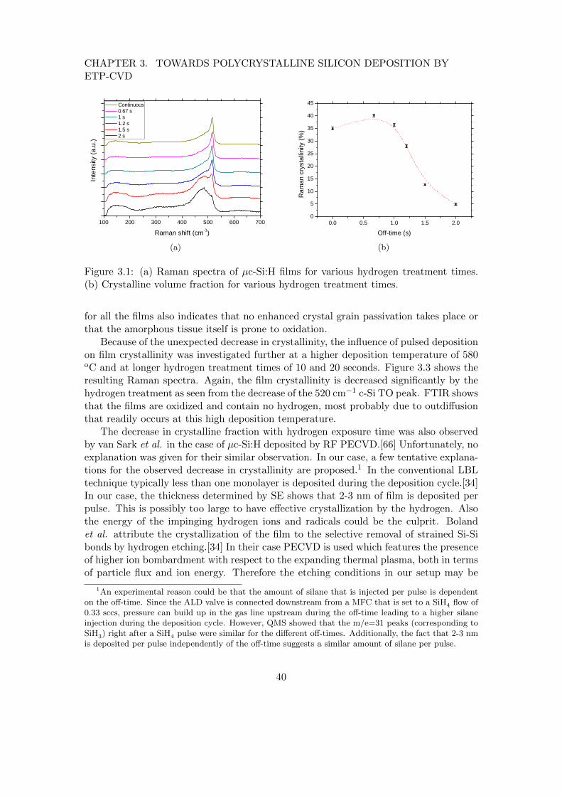
CHAPTER 3. TOWARDS POLYCRYSTALLINE SILICON DEPOSITION BYETP-CVD
1 0 0 2 0 0 3 0 0 4 0 0 5 0 0 6 0 0 7 0 0
Inten
sity (a
.u.)
R a m a n s h i f t ( c m - 1 )
C o n t i n u o u s 0 . 6 7 s 1 s 1 . 2 s 1 . 5 s 2 s
(a)
0 . 0 0 . 5 1 . 0 1 . 5 2 . 005
1 01 52 02 53 03 54 04 5
Rama
n crys
tallini
ty (%
)
O f f - t i m e ( s )(b)
Figure 3.1: (a) Raman spectra of µc-Si:H films for various hydrogen treatment times.(b) Crystalline volume fraction for various hydrogen treatment times.
for all the films also indicates that no enhanced crystal grain passivation takes place orthat the amorphous tissue itself is prone to oxidation.
Because of the unexpected decrease in crystallinity, the influence of pulsed depositionon film crystallinity was investigated further at a higher deposition temperature of 580oC and at longer hydrogen treatment times of 10 and 20 seconds. Figure 3.3 shows theresulting Raman spectra. Again, the film crystallinity is decreased significantly by thehydrogen treatment as seen from the decrease of the 520 cm−1 c-Si TO peak. FTIR showsthat the films are oxidized and contain no hydrogen, most probably due to outdiffusionthat readily occurs at this high deposition temperature.
The decrease in crystalline fraction with hydrogen exposure time was also observedby van Sark et al. in the case of µc-Si:H deposited by RF PECVD.[66] Unfortunately, noexplanation was given for their similar observation. In our case, a few tentative explana-tions for the observed decrease in crystallinity are proposed.1 In the conventional LBLtechnique typically less than one monolayer is deposited during the deposition cycle.[34]In our case, the thickness determined by SE shows that 2-3 nm of film is deposited perpulse. This is possibly too large to have effective crystallization by the hydrogen. Alsothe energy of the impinging hydrogen ions and radicals could be the culprit. Bolandet al. attribute the crystallization of the film to the selective removal of strained Si-Sibonds by hydrogen etching.[34] In their case PECVD is used which features the presenceof higher ion bombardment with respect to the expanding thermal plasma, both in termsof particle flux and ion energy. Therefore the etching conditions in our setup may be
1An experimental reason could be that the amount of silane that is injected per pulse is dependenton the off-time. Since the ALD valve is connected downstream from a MFC that is set to a SiH4 flow of0.33 sccs, pressure can build up in the gas line upstream during the off-time leading to a higher silaneinjection during the deposition cycle. However, QMS showed that the m/e=31 peaks (corresponding toSiH3) right after a SiH4 pulse were similar for the different off-times. Additionally, the fact that 2-3 nmis deposited per pulse independently of the off-time suggests a similar amount of silane per pulse.
40
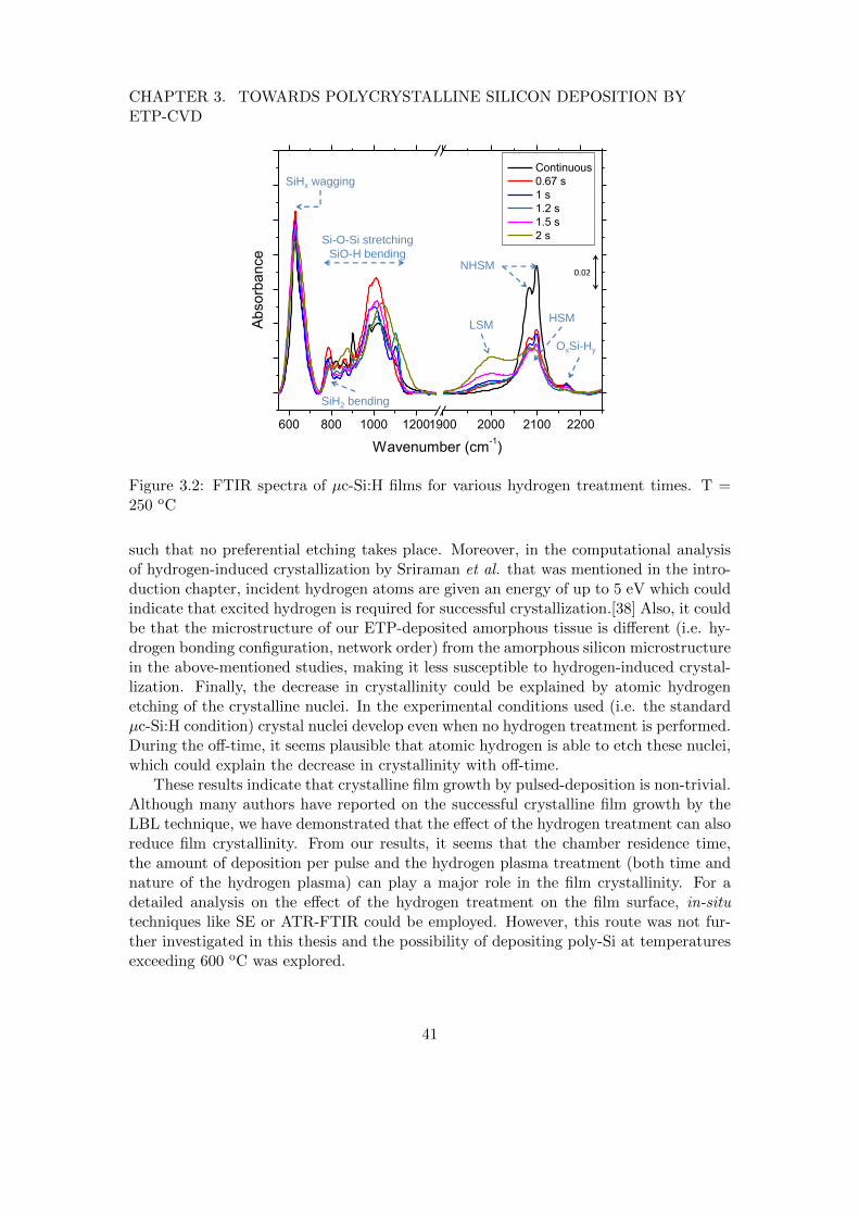
CHAPTER 3. TOWARDS POLYCRYSTALLINE SILICON DEPOSITION BYETP-CVD
600 800 1000 12001900 2000 2100 2200
Absorb
ance
Wavenumber (cm-1)
Continuous
0.67 s
1 s
1.2 s
1.5 s
2 s
SiHx wagging
Si-O-Si stretching
SiO-H bending
LSM
NHSM
HSM
OxSi-Hy
SiH2 bending
0.02
Figure 3.2: FTIR spectra of µc-Si:H films for various hydrogen treatment times. T =250 oC
such that no preferential etching takes place. Moreover, in the computational analysisof hydrogen-induced crystallization by Sriraman et al. that was mentioned in the intro-duction chapter, incident hydrogen atoms are given an energy of up to 5 eV which couldindicate that excited hydrogen is required for successful crystallization.[38] Also, it couldbe that the microstructure of our ETP-deposited amorphous tissue is different (i.e. hy-drogen bonding configuration, network order) from the amorphous silicon microstructurein the above-mentioned studies, making it less susceptible to hydrogen-induced crystal-lization. Finally, the decrease in crystallinity could be explained by atomic hydrogenetching of the crystalline nuclei. In the experimental conditions used (i.e. the standardµc-Si:H condition) crystal nuclei develop even when no hydrogen treatment is performed.During the off-time, it seems plausible that atomic hydrogen is able to etch these nuclei,which could explain the decrease in crystallinity with off-time.
These results indicate that crystalline film growth by pulsed-deposition is non-trivial.Although many authors have reported on the successful crystalline film growth by theLBL technique, we have demonstrated that the effect of the hydrogen treatment can alsoreduce film crystallinity. From our results, it seems that the chamber residence time,the amount of deposition per pulse and the hydrogen plasma treatment (both time andnature of the hydrogen plasma) can play a major role in the film crystallinity. For adetailed analysis on the effect of the hydrogen treatment on the film surface, in-situtechniques like SE or ATR-FTIR could be employed. However, this route was not fur-ther investigated in this thesis and the possibility of depositing poly-Si at temperaturesexceeding 600 oC was explored.
41
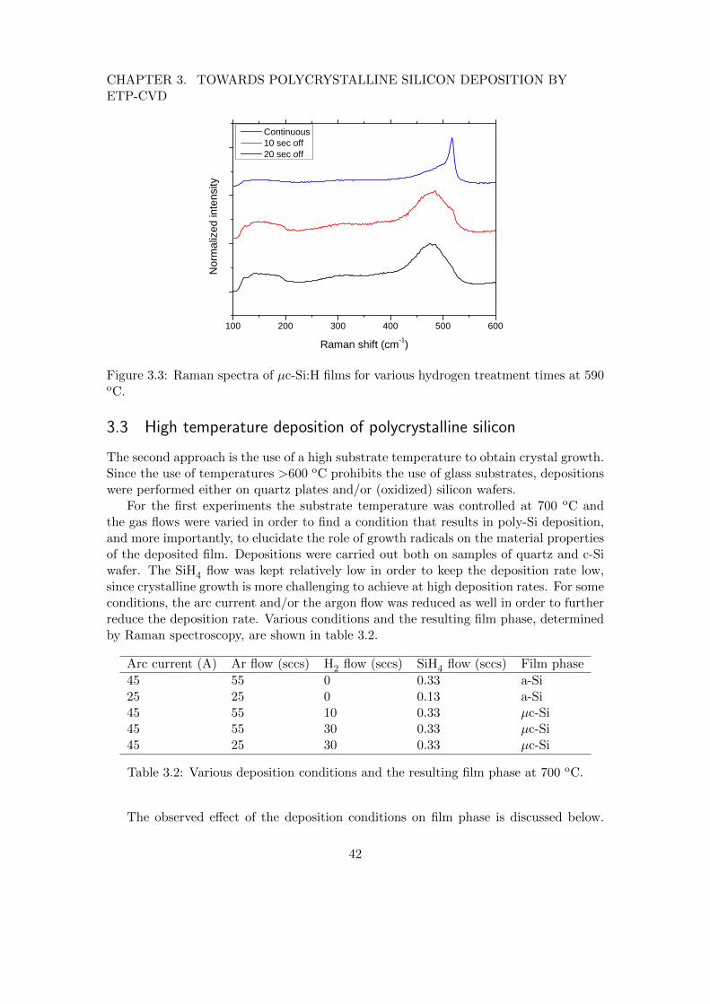
CHAPTER 3. TOWARDS POLYCRYSTALLINE SILICON DEPOSITION BYETP-CVD
1 0 0 2 0 0 3 0 0 4 0 0 5 0 0 6 0 0
Norm
alized
inten
sity
R a m a n s h i f t ( c m - 1 )
C o n t i n u o u s 1 0 s e c o f f 2 0 s e c o f f
Figure 3.3: Raman spectra of µc-Si:H films for various hydrogen treatment times at 590oC.
3.3 High temperature deposition of polycrystalline silicon
The second approach is the use of a high substrate temperature to obtain crystal growth.Since the use of temperatures >600 oC prohibits the use of glass substrates, depositionswere performed either on quartz plates and/or (oxidized) silicon wafers.
For the first experiments the substrate temperature was controlled at 700 oC andthe gas flows were varied in order to find a condition that results in poly-Si deposition,and more importantly, to elucidate the role of growth radicals on the material propertiesof the deposited film. Depositions were carried out both on samples of quartz and c-Siwafer. The SiH4 flow was kept relatively low in order to keep the deposition rate low,since crystalline growth is more challenging to achieve at high deposition rates. For someconditions, the arc current and/or the argon flow was reduced as well in order to furtherreduce the deposition rate. Various conditions and the resulting film phase, determinedby Raman spectroscopy, are shown in table 3.2.
Arc current (A) Ar flow (sccs) H2 flow (sccs) SiH4 flow (sccs) Film phase
45 55 0 0.33 a-Si25 25 0 0.13 a-Si45 55 10 0.33 µc-Si45 55 30 0.33 µc-Si45 25 30 0.33 µc-Si
Table 3.2: Various deposition conditions and the resulting film phase at 700 oC.
The observed effect of the deposition conditions on film phase is discussed below.
42
CHAPTER 3. TOWARDS POLYCRYSTALLINE SILICON DEPOSITION BYETP-CVD
From these experimental results, the role of growth radicals on the film phase is deduced,as will be discussed in the next section (3.3.1).
As seen from the table, for both conditions where no hydrogen is admixed in thearc the film phase is amorphous, even when using a very low arc current and low argonand silane flows. Adding high amounts of hydrogen (10 and 30 sccs) leads to a micro-crystalline phase, indicating once again the importance of hydrogen in achieving crystalgrowth.
Since these initial experiments at 700 oC did not result in the deposition of a poly-Sifilm, the substrate temperature was raised to 800 oC for further experiments. Table 3.3shows the resulting film phases at 800 oC for a different set of conditions.
Arc current (A) Ar flow (sccs) H2 flow (sccs) SiH4 flow (sccs) Film phase
45 55 0 0.1 a-Si45 55 5 0.33 µc-Si/poly-Si45 55 10 2.5 poly-Si45 55 10 10 a-Si
Table 3.3: Various deposition conditions and the resulting film phase at 800 oC.
Again, for the first condition with no hydrogen admixed in the arc, the film is amor-phous. However, two conditions that lead to a crystalline film were identified. For ahydrogen flow of 5 sccs and a silane flow of 0.33 sccs FTIR shows that the film is highlyoxidized. Also, Raman shows a very limited remaining amorphous content. However,the film produced using 10 sccs of hydrogen and 2.5 sccs shows no sign of amorphoustissue and is stable to oxidation, indicating a dense film.
The poly-Si film deposited by this initial unoptimized deposition condition has beenanalyzed by Raman spectroscopy, X-ray diffraction, AFM and scanning electron mi-croscopy (SEM). In the Raman spectrum (figure 3.4(a)) only the c-Si TO peak is visible,indicating full crystallinity. However, the TO peak is slightly shifted to 519 cm−1, whichcould indicate stress in the film.[67]
X-ray diffraction (figure 3.4(b)) reveals a very strong preferential orientation. The(220) peak at 47.4o 2θ is much higher than the (111) and (311) peak. The FWHM of the(220) peak is only 0.14o 2θ, whereas the (111) and (311) peaks are much broader, witha FWHM of 0.27 and 0.30o 2θ, respectively. This suggests a much larger perpendiculargrain size for (220)-oriented grains, which is a strong indication of the desirable columnargrowth, typical of (220) oriented films.
Cross-sectional SEM shows a film thickness of 2.5 µm (figure 3.5). Since the depo-sition time was 300 seconds, an unoptimized deposition rate in excess of 8 nm/s wasachieved, which is considerable for poly-Si deposition. It is noteworthy that when usingthe same plasma conditions but a lower substrate temperature of 400 oC, Kessels et al.obtained an amorphous silicon film at a deposition rate ∼3 nm/s.
Under these conditions, they found from aperture-well experiments that the overallsurface reaction probability was ∼0.3-0.4.[68] At 800 oC, the deposition rate is nearly
43
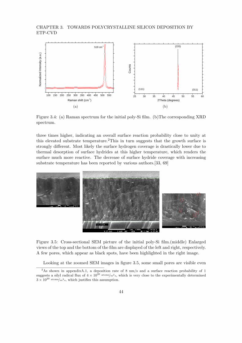
CHAPTER 3. TOWARDS POLYCRYSTALLINE SILICON DEPOSITION BYETP-CVD
1 0 0 1 5 0 2 0 0 2 5 0 3 0 0 3 5 0 4 0 0 4 5 0 5 0 0 5 5 0
No
rmaliz
ed In
tensity
(a.u.
)
R a m a n s h i f t ( c m - 1 )
5 1 9 c m - 1
(a)
2 5 3 0 3 5 4 0 4 5 5 0 5 5 6 0
( 3 1 1 )
( 2 2 0 )
Coun
ts
2 T h e t a ( d e g r e e s )
( 1 1 1 )
(b)
Figure 3.4: (a) Raman spectrum for the initial poly-Si film. (b)The corresponding XRDspectrum.
three times higher, indicating an overall surface reaction probability close to unity atthis elevated substrate temperature.2This in turn suggests that the growth surface isstrongly different. Most likely the surface hydrogen coverage is drastically lower due tothermal desorption of surface hydrides at this higher temperature, which renders thesurface much more reactive. The decrease of surface hydride coverage with increasingsubstrate temperature has been reported by various authors.[33, 69]
Figure 3.5: Cross-sectional SEM picture of the initial poly-Si film.(middle) Enlargedviews of the top and the bottom of the film are displayed of the left and right, respectively.A few pores, which appear as black spots, have been highlighted in the right image.
Looking at the zoomed SEM images in figure 3.5, some small pores are visible even
2As shown in appendixA.1, a deposition rate of 8 nm/s and a surface reaction probability of 1suggests a silyl radical flux of 4 × 10²⁰ atoms/m2s, which is very close to the experimentally determined3 × 1020 atoms/m2s, which justifies this assumption.
44
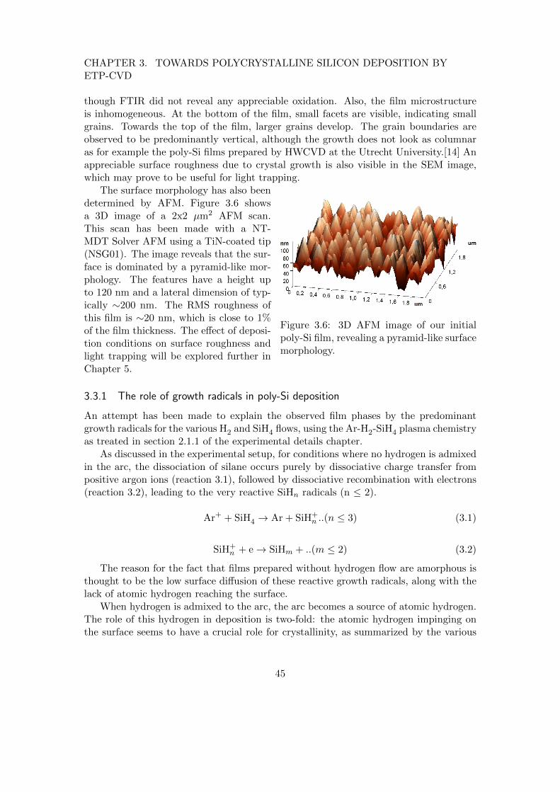
CHAPTER 3. TOWARDS POLYCRYSTALLINE SILICON DEPOSITION BYETP-CVD
though FTIR did not reveal any appreciable oxidation. Also, the film microstructureis inhomogeneous. At the bottom of the film, small facets are visible, indicating smallgrains. Towards the top of the film, larger grains develop. The grain boundaries areobserved to be predominantly vertical, although the growth does not look as columnaras for example the poly-Si films prepared by HWCVD at the Utrecht University.[14] Anappreciable surface roughness due to crystal growth is also visible in the SEM image,which may prove to be useful for light trapping.
Figure 3.6: 3D AFM image of our initialpoly-Si film, revealing a pyramid-like surfacemorphology.
The surface morphology has also beendetermined by AFM. Figure 3.6 showsa 3D image of a 2x2 µm2 AFM scan.This scan has been made with a NT-MDT Solver AFM using a TiN-coated tip(NSG01). The image reveals that the sur-face is dominated by a pyramid-like mor-phology. The features have a height upto 120 nm and a lateral dimension of typ-ically ∼200 nm. The RMS roughness ofthis film is ∼20 nm, which is close to 1%of the film thickness. The effect of deposi-tion conditions on surface roughness andlight trapping will be explored further inChapter 5.
3.3.1 The role of growth radicals in poly-Si deposition
An attempt has been made to explain the observed film phases by the predominantgrowth radicals for the various H2 and SiH4 flows, using the Ar-H2-SiH4 plasma chemistryas treated in section 2.1.1 of the experimental details chapter.
As discussed in the experimental setup, for conditions where no hydrogen is admixedin the arc, the dissociation of silane occurs purely by dissociative charge transfer frompositive argon ions (reaction 3.1), followed by dissociative recombination with electrons(reaction 3.2), leading to the very reactive SiHn radicals (n ≤ 2).
Ar+ + SiH4 → Ar + SiH+n ..(n ≤ 3) (3.1)
SiH+n + e→ SiHm + ..(m ≤ 2) (3.2)
The reason for the fact that films prepared without hydrogen flow are amorphous isthought to be the low surface diffusion of these reactive growth radicals, along with thelack of atomic hydrogen reaching the surface.
When hydrogen is admixed to the arc, the arc becomes a source of atomic hydrogen.The role of this hydrogen in deposition is two-fold: the atomic hydrogen impinging onthe surface seems to have a crucial role for crystallinity, as summarized by the various
45
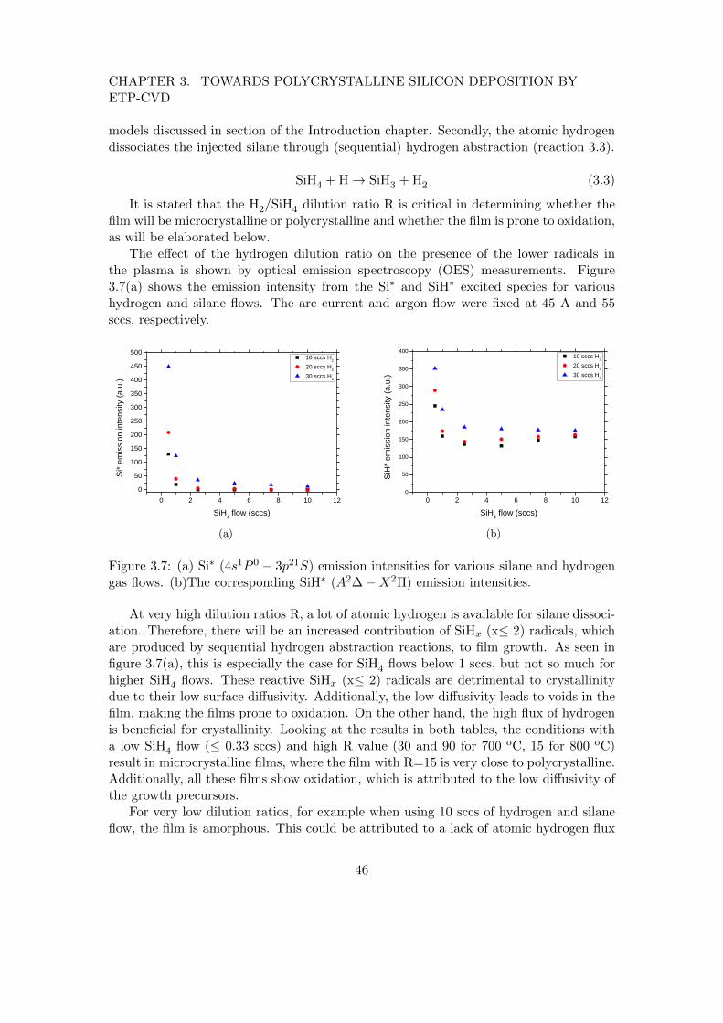
CHAPTER 3. TOWARDS POLYCRYSTALLINE SILICON DEPOSITION BYETP-CVD
models discussed in section of the Introduction chapter. Secondly, the atomic hydrogendissociates the injected silane through (sequential) hydrogen abstraction (reaction 3.3).
SiH4 + H→ SiH3 + H2 (3.3)
It is stated that the H2/SiH4 dilution ratio R is critical in determining whether thefilm will be microcrystalline or polycrystalline and whether the film is prone to oxidation,as will be elaborated below.
The effect of the hydrogen dilution ratio on the presence of the lower radicals inthe plasma is shown by optical emission spectroscopy (OES) measurements. Figure3.7(a) shows the emission intensity from the Si∗ and SiH∗ excited species for varioushydrogen and silane flows. The arc current and argon flow were fixed at 45 A and 55sccs, respectively.
0 2 4 6 8 1 0 1 20
5 01 0 01 5 02 0 02 5 03 0 03 5 04 0 04 5 05 0 0 1 0 s c c s H 2
2 0 s c c s H 2 3 0 s c c s H 2
Si* em
ission
inten
sity (a
.u.)
S i H 4 f l o w ( s c c s )
(a)
0 2 4 6 8 1 0 1 20
5 0
1 0 0
1 5 0
2 0 0
2 5 0
3 0 0
3 5 0
4 0 0 1 0 s c c s H 2 2 0 s c c s H 2 3 0 s c c s H 2
SiH* e
missi
on in
tensity
(a.u.
)
S i H 4 f l o w ( s c c s )
(b)
Figure 3.7: (a) Si∗ (4s1P 0 − 3p21S) emission intensities for various silane and hydrogengas flows. (b)The corresponding SiH∗ (A2∆−X2Π) emission intensities.
At very high dilution ratios R, a lot of atomic hydrogen is available for silane dissoci-ation. Therefore, there will be an increased contribution of SiHx (x≤ 2) radicals, whichare produced by sequential hydrogen abstraction reactions, to film growth. As seen infigure 3.7(a), this is especially the case for SiH4 flows below 1 sccs, but not so much forhigher SiH4 flows. These reactive SiHx (x≤ 2) radicals are detrimental to crystallinitydue to their low surface diffusivity. Additionally, the low diffusivity leads to voids in thefilm, making the films prone to oxidation. On the other hand, the high flux of hydrogenis beneficial for crystallinity. Looking at the results in both tables, the conditions witha low SiH4 flow (≤ 0.33 sccs) and high R value (30 and 90 for 700 oC, 15 for 800 oC)result in microcrystalline films, where the film with R=15 is very close to polycrystalline.Additionally, all these films show oxidation, which is attributed to the low diffusivity ofthe growth precursors.
For very low dilution ratios, for example when using 10 sccs of hydrogen and silaneflow, the film is amorphous. This could be attributed to a lack of atomic hydrogen flux
46
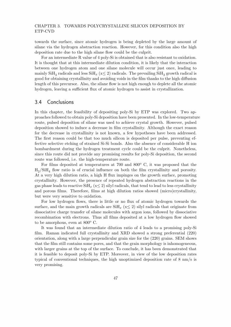
CHAPTER 3. TOWARDS POLYCRYSTALLINE SILICON DEPOSITION BYETP-CVD
towards the surface, since atomic hydrogen is being depleted by the large amount ofsilane via the hydrogen abstraction reaction. However, for this condition also the highdeposition rate due to the high silane flow could be the culprit.
For an intermediate R value of 4 poly-Si is obtained that is also resistant to oxidation.It is thought that at this intermediate dilution condition, it is likely that the interactionbetween one hydrogen atom and one silane molecule will occur just once, leading tomainly SiH3 radicals and less SiHx (x≤ 2) radicals. The prevailing SiH3 growth radical isgood for obtaining crystallinity and avoiding voids in the film thanks to the high diffusionlength of this precursor. Also, the silane flow is not high enough to deplete all the atomichydrogen, leaving a sufficient flux of atomic hydrogen to assist in crystallization.
3.4 Conclusions
In this chapter, the feasibility of depositing poly-Si by ETP was explored. Two ap-proaches followed to obtain poly-Si deposition have been presented. In the low-temperatureroute, pulsed deposition of silane was used to achieve crystal growth. However, pulseddeposition showed to induce a decrease in film crystallinity. Although the exact reasonfor the decrease in crystallinity is not known, a few hypotheses have been addressed.The first reason could be that too much silicon is deposited per pulse, preventing ef-fective selective etching of strained Si-Si bonds. Also the absence of considerable H ionbombardment during the hydrogen treatment cycle could be the culprit. Nonetheless,since this route did not provide any promising results for poly-Si deposition, the secondroute was followed, i.e. the high-temperature route.
For films deposited at temperatures at 700 and 800o C, it was proposed that theH2/SiH4 flow ratio is of crucial influence on both the film crystallinity and porosity.At a very high dilution ratio, a high H flux impinges on the growth surface, promotingcrystallinity. However, the presence of repeated hydrogen abstraction reactions in thegas phase leads to reactive SiHx (x≤ 2) silyl radicals, that tend to lead to less crystallinityand porous films. Therefore, films at high dilution ratios showed (micro)crystallinity,but were very sensitive to oxidation.
For low hydrogen flows, there is little or no flux of atomic hydrogen towards thesurface, and the main growth radicals are SiHx (x≤ 2) silyl radicals that originate fromdissociative charge transfer of silane molecules with argon ions, followed by dissociativerecombination with electrons. Thus all films deposited at a low hydrogen flow showedto be amorphous, even at 800o C.
It was found that an intermediate dilution ratio of 4 leads to a promising poly-Sifilm. Raman indicated full crystallinity and XRD showed a strong preferential (220)orientation, along with a large perpendicular grain size for the (220) grains. SEM showsthat the film still contains some pores, and that the grain morphology is inhomogeneous,with larger grains at the top of the surface. To conclude, it has been demonstrated thatit is feasible to deposit poly-Si by ETP. Moreover, in view of the low deposition ratestypical of conventional techniques, the high unoptimized deposition rate of 8 nm/s isvery promising.
47
Chapter 4
On the growth mechanism of poly-Sideposited by ETP
4.1 Introduction
In the previous chapter, initial results on the direct deposition of poly-Si were presented.XRD showed a strong preferential (220) growth, and a strongly inhomogeneous grainmorphology was observed in the SEM image, with small grains at the bottom of the filmgrowing to larger grains towards the top of the film. The aim of this chapter is to gaininsight in the evolution of the grain morphology and orientation during deposition.
The dependence of the preferential orientation on the film thickness has been investi-gated. In literature it is common to report preferential orientations of poly-Si films, butvery limited studies are dedicated to the evolution of the preferential orientation withfilm thickness. Since SEM revealed an evolution of the grain morphology from smallcrystals to more columnar growth, it is speculated that a change in preferential orien-tation may occur. XRD has been performed on a thickness series to determine whetherthe preferential (220) orientation is present from the onset of crystal growth or whetherit develops during film deposition.
Furthermore, in-situ SE has been employed for the characterization of film growth.Spectroscopic ellipsometry is able to distinguish between amorphous and crystallinegrowth, and is therefore an excellent tool to check for the presence of incubation amor-phous layer in our films, as already observed in µc-Si:H growth. The growth of poly-Siunder various deposition conditions has been monitored by in-situ SE in order to inves-tigate the presence of an incubation layer (and its thickness), and its dependence on thedeposition conditions.
This chapter is concluded by a proposed model able to explain the observed inho-mogeneous grain morphology as seen in the SEM image, and also the different phases offilm growth that were found from XRD measurements on the thickness series and thein-situ SE measurements. Furthermore, this model has been verified by TEM imaging.
48
CHAPTER 4. ON THE GROWTH MECHANISM OF POLY-SI DEPOSITED BYETP
4.2 Experimental details
A thickness series for the ex-situ XRD analysis has been deposited using the initialdeposition conditions defined in the previous chapter. Depositions were carried out onquartz substrates. Deposition times were varied between 10 and 1200 seconds in orderto have a large range in thickness (∼80-9600 nm).
For in-situ SE analysis, oxidized (∼ 450 nm) silicon wafers were used for deposition.The reason for using oxidized wafers instead of bare silicon wafers is that the SiO2 layergenerates a better contrast between the silicon wafer and the poly-Si film, essential forthe SE modeling. Also, the surface of an oxidized wafer is comparable to that of quartz,which can be of importance for crystal growth. A scan time of one second was used,as this was found to be a good compromise between temporal resolution and signal-to-noise ratio. Note that since deposition rates in the order of 10 nm/s are achieved,the film thickness increases on the order of 10 nm during an SE measurement with ascan time of 1 s. Therefore these measurements represent the ’effective’ film duringan acquisition. For the in-situ SE analysis, the initial poly-Si deposition condition wastaken as the starting point. From this starting condition, the silane flow has been variedbetween 1 and 7.5 sccs and the substrate temperature was set to either 690 or 740 oC.Additionally, two depositions have been carried out at a higher hydrogen flow of 30 sccs.The deposition time was kept constant at 200 s.
4.3 Results and discussion
4.3.1 X-ray diffraction on a poly-Si thickness series
The thickness series that was deposited for the ex-situ XRD analysis has first beencharacterized by Raman spectroscopy, which showed full crystallinity for all the films.Even the film with a deposition time of just 10 s shows no amorphous signature. Sincethis film has a thickness of ∼80 nm, which is much less than the penetration depth ofthe Raman laser, this suggests that there is no (or a very thin) amorphous incubationlayer.
XRD gonio measurements in the 20-60 o 2θ range have been carried out on thisthickness series. The resulting peak intensities of the (111), (220) and (311) diffractionplanes for these films are shown in figure 4.1. The peak intensities have been obtainedby integration of the area under the peak (after baseline subtraction) and subsequentnormalization to the corresponding powder diffraction peak intensity.
Two regimes in the film growth can be observed. For deposition times t < 50 s, thethree peak intensities overlap (see inset in figure 4.1), indicating a completely randomgrain orientation. For larger deposition times the (220) intensity increases, whereas the(111) and (311) intensities remain constant.
Since Raman shows no sign of an amorphous incubation layer, these results suggesta nucleation of randomly oriented crystal grains at the onset of film growth. After acertain thickness, preferential growth of (220) grains takes over, resulting in a linearincrease of (220) intensity with thickness.
49
CHAPTER 4. ON THE GROWTH MECHANISM OF POLY-SI DEPOSITED BYETP
0 200 400 600 800 1000 1200
(111)
(220)
(311)
Pe
ak in
ten
sity/p
ow
de
r d
iffr
actio
n (
a.u
.)
Deposition time (sec)
0 20 40 60 80 100 120
Pe
ak in
ten
sity/p
ow
de
r d
iffr
actio
n (
a.u
.)
Deposition time (sec)
Figure 4.1: Peak intensities of the (111), (220) and (311) diffraction peaks for variousdeposition times. An enlarged view for short deposition times is shown in the inset. Forthis condition, the deposition rate was ∼8 nm/s.
4.3.2 Monitoring poly-Si growth by in-situ SE
The poly-Si growth has been investigated further with in-situ SE. From the XRD resultsit is known that there is a transition from a random crystal growth to a preferential (220)growth. It is hypothesized that the preferential (220) growth could originate from a largercrystal growth rate for this orientation with respect to the other orientations. If this istrue, it may be possible to see an increase in deposition rate when going from randomgrowth to preferential (220) growth. In-situ SE was used to investigate this, as it is anexcellent tool to monitor film thickness during growth. Additionally, it can be used todiscriminate between amorphous and crystalline growth, allowing for an investigationof an amorphous incubation layer, if present. The model used for SE modeling in theCompleteEASE software is presented in the in-set on page 51.
50
CHAPTER 4. ON THE GROWTH MECHANISM OF POLY-SI DEPOSITED BYETP
SE model for poly-Si
Silicon substrate
Poly-Si (B-spline)
Surface roughness
(graded, coupled to poly-Si)
Oxide (Sellmeier)
For SE modeling of the film, the following layers have been implemented in theCompleteEASE software.
• Silicon substrate
A temperature-dependent silicon substrate dielectric function was appliedto take into account the changes in the substrate at high deposition tem-peratures.
• Oxide layer
The wafer oxide layer was modeled by the Sellmeier equation. A Sellmeieris used to fit the dispersion of light in an optically transparent medium.
• Poly-Si layer
The optical response of the deposited layer is fitted by a B-spline. Inthis way, the effective dielectric function of the deposited film can bedetermined, making it possible to distinguish between amorphous andcrystalline growth.
• Surface roughness
The surface roughness has been modeled by a 5-layer graded EMA layer.The two EMA constituents are voids and a medium of which the dielec-tric function is coupled to the bulk layer. This approach, instead of thestandard roughness model (50% voids, 50% material), was required for ob-taining satisfactory fit results. This is expected to originate from the factthat the surface morphology is pyramid-like, as seen in the AFM image offigure 3.6. This is confirmed by the fact that during fitting, the gradingresults in an increase of void content as a function of the roughness layerthickness.
51
CHAPTER 4. ON THE GROWTH MECHANISM OF POLY-SI DEPOSITED BYETP
Since in-situ SE is used to discriminate between amorphous and crystalline growth,it is instructive to look at the dielectric functions of these silicon phases. To this end,simulated ε2 curves have been generated with the CompleteEASE software, as shown infigure 4.2(a).
1.5 2.0 2.5 3.0 3.5 4.0 4.5 5.0
0
5
10
15
20
25
30
35
40
45
50
2
Energy (eV)
c-Si, 25 oC
c-Si, 25 oC, 10 nm roughness
c-Si, 800 oC
a-Si E1
E2
(a)
1 2 3 4 5 6 7
10
100
1000
Pe
ne
tra
tio
n d
ep
th (
nm
)
Photon energy (eV)
E1 E2
(b)
Figure 4.2: (a) Simulated ε2 curves of c-Si at room temperature, c-Si at 800 oC, c-Siwith 10 nm roughness and of amorphous silicon.(b) Spectral penetration depth of lightin crystalline silicon.
The black spectrum corresponds to the dielectric function of crystalline silicon atroom temperature. Two absorption peaks are observed. As can be seen in figure 4.3,these correspond to the direct E1 and E2 transitions at the Λ and X points in the banddiagram of c-Si, respectively.[63, 70]
Figure 4.3: Band diagram of crys-talline silicon.[70]
The red curve represents the dielectric functionof a silicon wafer with 10 nm of surface roughness(50% c-Si, 50% voids). The roughness has a cleareffect on the dielectric response. The E1 and E2peaks are seen to decrease and there is an apparentshift to lower energies. This decrease is ascribed tothe void content of the roughness layer. Since thepenetration depth of the light is ≤20 nm at theenergies of the E1 and E2 peaks (see figure 4.2(b)),the voids (ε2=0) in the roughness layer constitutea large part of the effective ε2. Also, since thepenetration depth at the energy of the E2 peak islower than at the E1 peak, the effect of roughnesson the E2 peak is more prominent, explaining whythe E1 peak is higher than the E2 peak for therough silicon surface. The dielectric function of c-Si also has a clear dependence on the temperature,as can be seen from the blue curve. At higher temperatures, there is an overall shift
52
CHAPTER 4. ON THE GROWTH MECHANISM OF POLY-SI DEPOSITED BYETP
to lower energies. Amorphous silicon (teal line) has a broad feature in its ε2 spectrum,represented by a Tauc-Lorentz oscillator.
1 . 5 2 . 0 2 . 5 3 . 0 3 . 5 4 . 0 4 . 5 5 . 0
0
5
1 0
1 5
2 0
2 5
3 0
ε 2
E n e r g y ( e V )
8 s e c o n d s 1 8 s e c o n d s 4 5 s e c o n d s 1 2 3 s e c o n d s
Figure 4.4: Evolution of the effective dielectric function of the bulk layer, as obtainedfrom a B-spline fit.
In-situ SE was performed by deposition on an oxidized wafer using our initial poly-Sicondition. From the b-spline fit in the model, it is possible to see the evolution of thefilm dielectric function during deposition, as shown in figure 4.4. It is observed that thefilm phase during the first 17 s of deposition (corresponding to a thickness of 160 nm) isamorphous, as can be seen by comparison with the teal line in figure 4.2(a). After thisthickness, the film dielectric function gradually develops towards the one correspondingto poly-Si, as observed by the development of the two distinct E1 and E2 absorptionpeaks. Note that these peaks only reveal information on the first ∼20 nm of film due tothe low penetration depth at this photon energy. With increasing deposition time, theE1 and E2 peaks decrease and the E1 peak becomes more prominent than the E2 peak,indicating the development of an appreciable surface roughness.
The fact that SE shows an amorphous growth for the first ∼160 nm of film is remark-able, since films with a deposition time of 10 and 20 seconds (corresponding to a filmthickness of ∼80 and ∼160 nm, respectively) for the XRD thickness series are completelycrystalline, as inferred from Raman measurements.
The film thickness and roughness during deposition have been determined by fit-ting of the SE data. The result is shown in figure 4.5. The film thickness is seen toincrease linearly, without a clear variation of deposition rate at the transition from arandomly-oriented to a (220)-oriented film. However, the film roughness evolution showsa remarkable feature. A prominent dip is visible, which has a minimum occurring atabout 17 s of deposition. This dip in roughness occurs precisely where the transitionfrom amorphous to crystalline growth is seen in the b-spline fit, indicating a correlationbetween the two phenomena.
53
CHAPTER 4. ON THE GROWTH MECHANISM OF POLY-SI DEPOSITED BYETP
0 5 0 1 0 0 1 5 0- 2 0 0
02 0 04 0 06 0 08 0 0
1 0 0 01 2 0 01 4 0 0
T h i c k n e s s ( n m ) R o u g h n e s s ( n m )
D e p o s i t i o n t i m e ( s )
Thick
ness
(nm)
0
2
4
6
8
1 0
1 2
SE roughness (nm)
Figure 4.5: Evolution of the film thickness and roughness during deposition, as deter-mined from in-situ SE.
Fujiwara et al. reported on a very similar observation in the deposition of µc-Si:Hby PECVD in several papers.[63, 71, 72, 73] They investigated crystal nucleation intheir (220)-oriented µc-Si:H by a combination of in-situ SE, in-situ attenuated totalreflection Fourier transform infrared spectroscopy (ATR-FTIR), stress measurementsand TEM. Just like in our case, they observed a dip in roughness in the SE data andoccurrence of this dip corresponds to the onset of crystal growth, as verified by TEM.
Si
DB
Si
H
Sid-complex
Figure 4.6: Schematic ofhydrogen incorporated in astrained Si-Si surface bond,forming a Sid-complex.[71]
Also, they found a decrease in this transition thick-ness with an increasing hydrogen dilution, suggesting aprominent role of hydrogen in nucleation. In the ATR-FTIR data an increase of a Si-H mode at ∼1937 cm−1
corresponding to a so-called Sid-complex is observedduring deposition up to the amorphous-crystalline tran-sition, followed by a sharp decrease right after the tran-sition. The Sid-complex corresponds to hydrogen in-serted into strained Si-Si bonds, as shown in figure 4.6.A linear correlation between the Sid-complex mode in-tensity with film stress was found. Also, it was observedthat for varying deposition conditions crystal nucleationalways occurred at a film stress of ∼750-800 MPa.
From these experimental observations, they pro-posed the following nucleation mechanism for their µc-Si:H films. During deposition, atomic hydrogen inserts into strained Si-Si bonds to formSid-complexes, thereby increasing film stress. Due to the increased film stress, the subse-quent deposited layers will have more strained Si-Si bonds, facilitating the formation ofmore Sid-complexes. This positive feedback loop leads to an increase of film stress dur-ing deposition. At a critical film stress, the film surface rearranges and relaxes, leading
54
CHAPTER 4. ON THE GROWTH MECHANISM OF POLY-SI DEPOSITED BYETP
to a minimum in roughness and is accompanied by the formation of crystal nuclei.Their proposed nucleation mechanism can shed some light on the question why the
pulsed deposition of the previous chapter did not result in an enhanced crystallinity.In conventional LBL deposition a sub-monolayer of deposited silicon is treated withhydrogen, resulting in the formation of Sid-complexes and a corresponding increase infilm stress. However, in our depositions typically 2-3 nm of a-Si:H per pulse was rapidlydeposited on top of a a-Si:H surface that is treated with a hydrogen plasma. It isspeculated therefore, that under our experimental pulsing conditions there is no buildup of stress, leading to nucleation.
It is thought that also in our case the dip in roughness corresponds to a nucleationevent. The main reasons are the similarities in roughness evolution between our exper-iments and those of Fujiwara et al. and also the simultaneity of the transition fromamorphous to crystalline growth and the roughness dip. To investigate this claim fur-ther, the experimental window has been further extended. At a hydrogen flow of 10sccs, two substrate temperatures of 690 and 740 oC were considered, and the silane flowwas varied between 1 and 7.5 sccs. The resulting deposition rates, as determined fromin-situ SE, are shown in figure 4.7.
0 1 2 3 4 5 6 7 8
0
2
4
6
8
10
12
14
16
18
20
Depositio
n r
ate
(nm
/s)
SiH4 flow (sccs)
690 oC
740 oC
Amorphous
Figure 4.7: Deposition rate as a function of silane flow at a H2 flow of 10 sccs.
The deposition rate is seen to increase with increasing silane flow, which is attributedto an increased growth precursor flux. The deposition rate also increases with tempera-ture, indicating that growth is thermally activated. For a silane flow of 7.5 sccs at 690 oCthe film is amorphous, which could indicate a too high deposition rate for crystal growthand/or a depletion of atomic hydrogen by silane. Note that a deposition rate of morethan 18 nm/s is achieved at 740 oC and a SiH4 flow of 7.5 sccs, which is considerable.
Figure 4.8 shows the evolution of film roughness as function of the film thicknessfor these samples. At 690 oC, the film with 1 sccs of silane flow seems to have twodips in roughness. However, the amorphous-crystalline transition in the B-spline fit isobserved for the second dip at 275 nm of film thickness, indicating that the first dip is
55
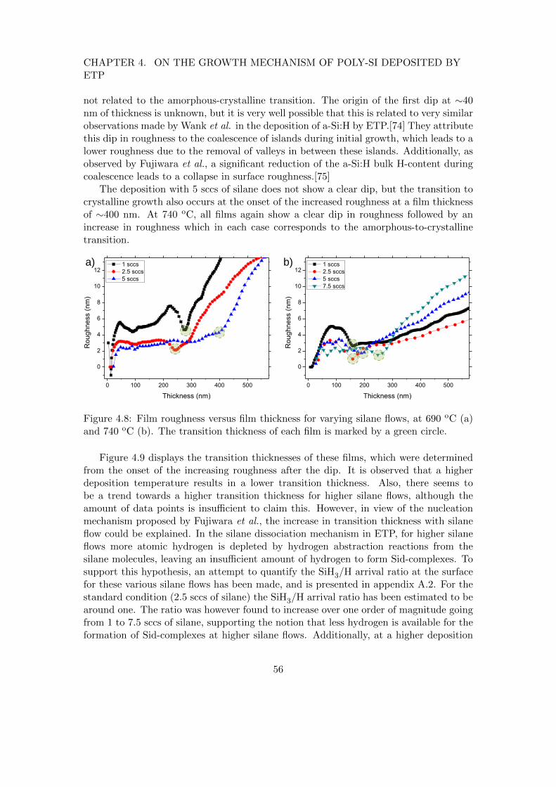
CHAPTER 4. ON THE GROWTH MECHANISM OF POLY-SI DEPOSITED BYETP
not related to the amorphous-crystalline transition. The origin of the first dip at ∼40nm of thickness is unknown, but it is very well possible that this is related to very similarobservations made by Wank et al. in the deposition of a-Si:H by ETP.[74] They attributethis dip in roughness to the coalescence of islands during initial growth, which leads to alower roughness due to the removal of valleys in between these islands. Additionally, asobserved by Fujiwara et al., a significant reduction of the a-Si:H bulk H-content duringcoalescence leads to a collapse in surface roughness.[75]
The deposition with 5 sccs of silane does not show a clear dip, but the transition tocrystalline growth also occurs at the onset of the increased roughness at a film thicknessof ∼400 nm. At 740 oC, all films again show a clear dip in roughness followed by anincrease in roughness which in each case corresponds to the amorphous-to-crystallinetransition.
0 100 200 300 400 500
0
2
4
6
8
10
12
SE Roughness vs Thickness (690 oC)
Ro
ug
hn
ess (
nm
)
Thickness (nm)
1 sccs
2.5 sccs
5 sccs
0 100 200 300 400 500
0
2
4
6
8
10
12
SE Roughness vs Thickness (740 oC)
Ro
ug
hn
ess (
nm
)
Thickness (nm)
1 sccs
2.5 sccs
5 sccs
7.5 sccs
a) b)
Figure 4.8: Film roughness versus film thickness for varying silane flows, at 690 oC (a)and 740 oC (b). The transition thickness of each film is marked by a green circle.
Figure 4.9 displays the transition thicknesses of these films, which were determinedfrom the onset of the increasing roughness after the dip. It is observed that a higherdeposition temperature results in a lower transition thickness. Also, there seems tobe a trend towards a higher transition thickness for higher silane flows, although theamount of data points is insufficient to claim this. However, in view of the nucleationmechanism proposed by Fujiwara et al., the increase in transition thickness with silaneflow could be explained. In the silane dissociation mechanism in ETP, for higher silaneflows more atomic hydrogen is depleted by hydrogen abstraction reactions from thesilane molecules, leaving an insufficient amount of hydrogen to form Sid-complexes. Tosupport this hypothesis, an attempt to quantify the SiH3/H arrival ratio at the surfacefor these various silane flows has been made, and is presented in appendix A.2. For thestandard condition (2.5 sccs of silane) the SiH3/H arrival ratio has been estimated to bearound one. The ratio was however found to increase over one order of magnitude goingfrom 1 to 7.5 sccs of silane, supporting the notion that less hydrogen is available for theformation of Sid-complexes at higher silane flows. Additionally, at a higher deposition
56
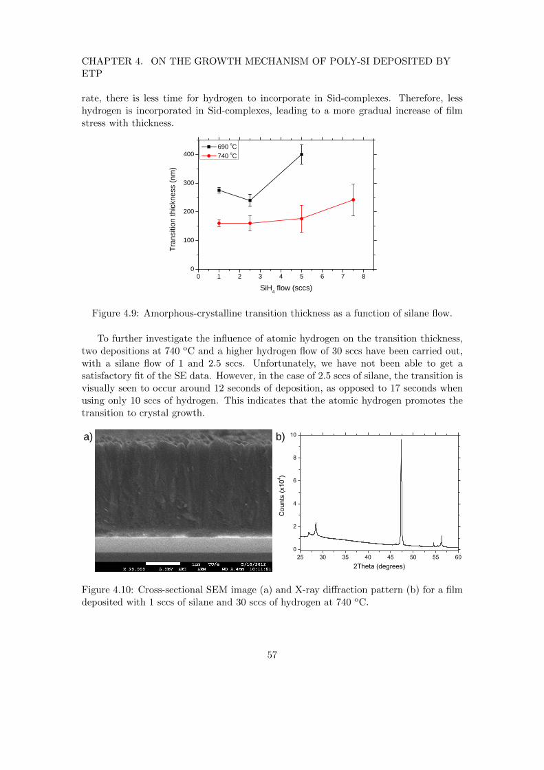
CHAPTER 4. ON THE GROWTH MECHANISM OF POLY-SI DEPOSITED BYETP
rate, there is less time for hydrogen to incorporate in Sid-complexes. Therefore, lesshydrogen is incorporated in Sid-complexes, leading to a more gradual increase of filmstress with thickness.
0 1 2 3 4 5 6 7 80
1 0 0
2 0 0
3 0 0
4 0 0
Trans
ition t
hickn
ess (
nm)
S i H 4 f l o w ( s c c s )
6 9 0 o C 7 4 0 o C
Figure 4.9: Amorphous-crystalline transition thickness as a function of silane flow.
To further investigate the influence of atomic hydrogen on the transition thickness,two depositions at 740 oC and a higher hydrogen flow of 30 sccs have been carried out,with a silane flow of 1 and 2.5 sccs. Unfortunately, we have not been able to get asatisfactory fit of the SE data. However, in the case of 2.5 sccs of silane, the transition isvisually seen to occur around 12 seconds of deposition, as opposed to 17 seconds whenusing only 10 sccs of hydrogen. This indicates that the atomic hydrogen promotes thetransition to crystal growth.
25 30 35 40 45 50 55 60
0
2
4
6
8
10
Counts
(x10
4)
2Theta (degrees)
a) b)
Figure 4.10: Cross-sectional SEM image (a) and X-ray diffraction pattern (b) for a filmdeposited with 1 sccs of silane and 30 sccs of hydrogen at 740 oC.
57
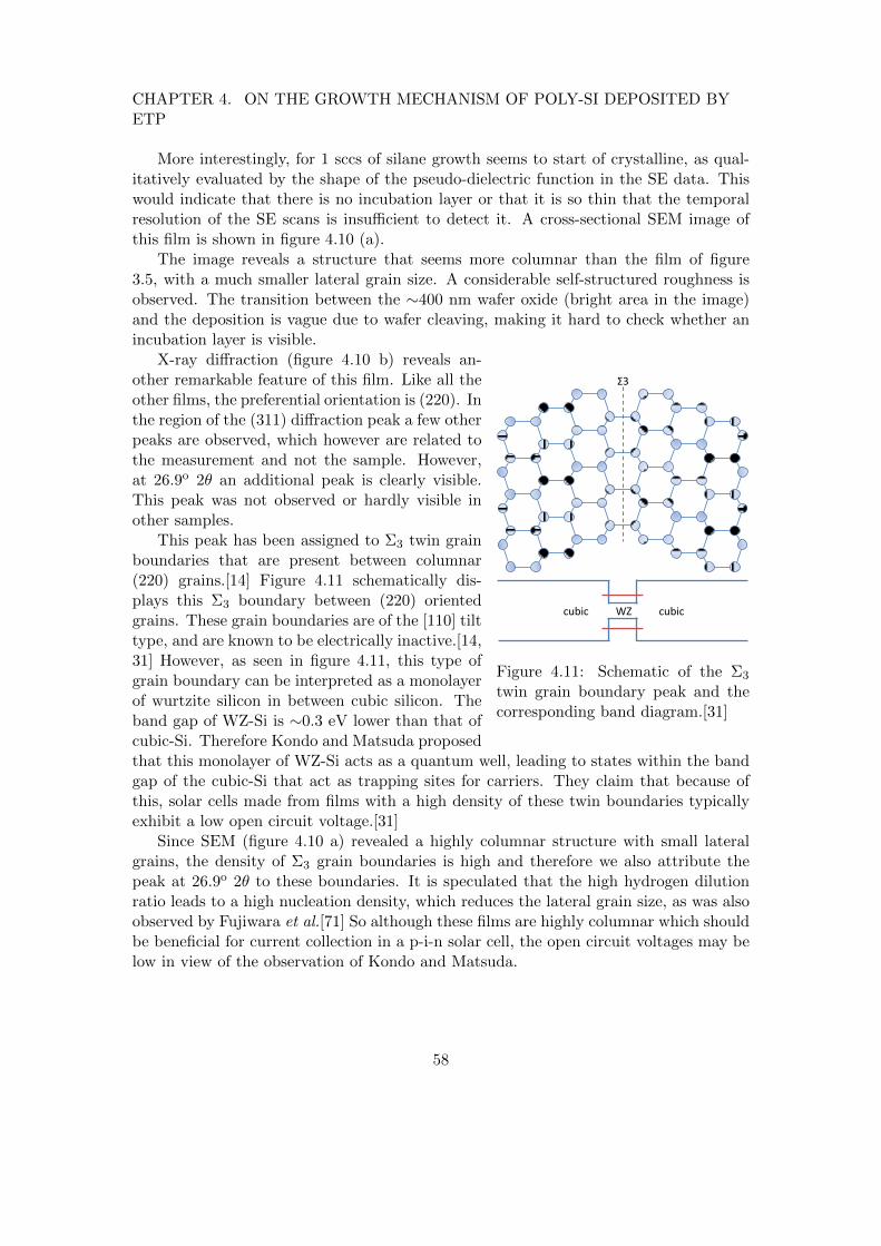
CHAPTER 4. ON THE GROWTH MECHANISM OF POLY-SI DEPOSITED BYETP
More interestingly, for 1 sccs of silane growth seems to start of crystalline, as qual-itatively evaluated by the shape of the pseudo-dielectric function in the SE data. Thiswould indicate that there is no incubation layer or that it is so thin that the temporalresolution of the SE scans is insufficient to detect it. A cross-sectional SEM image ofthis film is shown in figure 4.10 (a).
The image reveals a structure that seems more columnar than the film of figure3.5, with a much smaller lateral grain size. A considerable self-structured roughness isobserved. The transition between the ∼400 nm wafer oxide (bright area in the image)and the deposition is vague due to wafer cleaving, making it hard to check whether anincubation layer is visible.
Σ3
cubic WZ cubic
Figure 4.11: Schematic of the Σ3
twin grain boundary peak and thecorresponding band diagram.[31]
X-ray diffraction (figure 4.10 b) reveals an-other remarkable feature of this film. Like all theother films, the preferential orientation is (220). Inthe region of the (311) diffraction peak a few otherpeaks are observed, which however are related tothe measurement and not the sample. However,at 26.9o 2θ an additional peak is clearly visible.This peak was not observed or hardly visible inother samples.
This peak has been assigned to Σ3 twin grainboundaries that are present between columnar(220) grains.[14] Figure 4.11 schematically dis-plays this Σ3 boundary between (220) orientedgrains. These grain boundaries are of the [110] tilttype, and are known to be electrically inactive.[14,31] However, as seen in figure 4.11, this type ofgrain boundary can be interpreted as a monolayerof wurtzite silicon in between cubic silicon. Theband gap of WZ-Si is ∼0.3 eV lower than that ofcubic-Si. Therefore Kondo and Matsuda proposedthat this monolayer of WZ-Si acts as a quantum well, leading to states within the bandgap of the cubic-Si that act as trapping sites for carriers. They claim that because ofthis, solar cells made from films with a high density of these twin boundaries typicallyexhibit a low open circuit voltage.[31]
Since SEM (figure 4.10 a) revealed a highly columnar structure with small lateralgrains, the density of Σ3 grain boundaries is high and therefore we also attribute thepeak at 26.9o 2θ to these boundaries. It is speculated that the high hydrogen dilutionratio leads to a high nucleation density, which reduces the lateral grain size, as was alsoobserved by Fujiwara et al.[71] So although these films are highly columnar which shouldbe beneficial for current collection in a p-i-n solar cell, the open circuit voltages may below in view of the observation of Kondo and Matsuda.
58
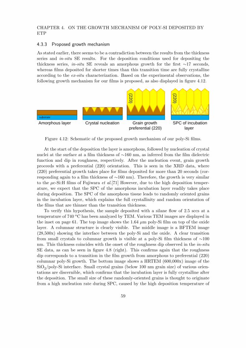
CHAPTER 4. ON THE GROWTH MECHANISM OF POLY-SI DEPOSITED BYETP
4.3.3 Proposed growth mechanism
As stated earlier, there seems to be a contradiction between the results from the thicknessseries and in-situ SE results. For the deposition conditions used for depositing thethickness series, in-situ SE reveals an amorphous growth for the first ∼17 seconds,whereas films deposited for shorter times than this transition time are fully crystallineaccording to the ex-situ characterization. Based on the experimental observations, thefollowing growth mechanism for our films is proposed, as also displayed in figure 4.12.
substrate
Amorphous layer Crystal nucleation Grain growth SPC of incubation
preferential (220) layer
(22
0)
(22
0)
Figure 4.12: Schematic of the proposed growth mechanism of our poly-Si films.
At the start of the deposition the layer is amorphous, followed by nucleation of crystalnuclei at the surface at a film thickness of ∼160 nm, as inferred from the film dielectricfunction and dip in roughness, respectively. After the nucleation event, grain growthproceeds with a preferential (220) orientation. This is seen in the XRD data, where(220) preferential growth takes place for films deposited for more than 20 seconds (cor-responding again to a film thickness of ∼160 nm). Therefore, the growth is very similarto the µc-Si:H films of Fujiwara et al.[71] However, due to the high deposition temper-ature, we expect that the SPC of the amorphous incubation layer readily takes placeduring deposition. The SPC of the amorphous tissue leads to randomly oriented grainsin the incubation layer, which explains the full crystallinity and random orientation ofthe films that are thinner than the transition thickness.
To verify this hypothesis, the sample deposited with a silane flow of 2.5 sccs at atemperature of 740 oC has been analyzed by TEM. Various TEM images are displayed inthe inset on page 61. The top image shows the 1.64 µm poly-Si film on top of the oxidelayer. A columnar structure is clearly visible. The middle image is a BFTEM image(28,500x) showing the interface between the poly-Si and the oxide. A clear transitionfrom small crystals to columnar growth is visible at a poly-Si film thickness of ∼100nm. This thickness coincides with the onset of the roughness dip observed in the in-situSE data, as can be seen in figure 4.8 (right). This confirms again that the roughnessdip corresponds to a transition in the film growth from amorphous to preferential (220)columnar poly-Si growth. The bottom image shows a HRTEM (600,000x) image of theSiO2/poly-Si interface. Small crystal grains (below 100 nm grain size) of various orien-tations are discernible, which confirms that the incubation layer is fully crystalline afterthe deposition. The small size of these randomly-oriented grains is thought to originatefrom a high nucleation rate during SPC, caused by the high deposition temperature of
59

CHAPTER 4. ON THE GROWTH MECHANISM OF POLY-SI DEPOSITED BYETP
740 o which is well above the crystallization temperature of amorphous silicon (∼ 600oC).
An experiment that could further support this growth model would be the depositionof a very thin amorphous layer (thinner than the amorphous-crystalline transition thick-ness) at the standard poly-Si condition and monitoring the film phase by in-situ SE.The model predicts that SPC of this thin amorphous layer should take place within 200seconds (which was our standard deposition time) at the high deposition temperature.
60
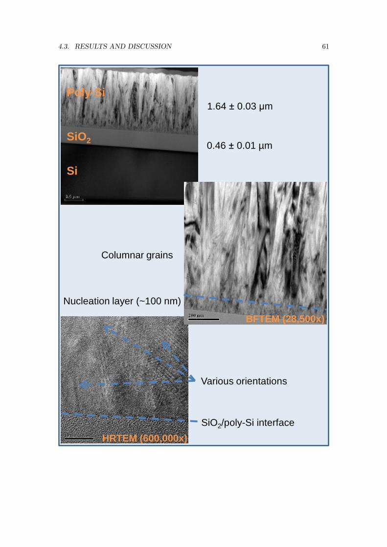
4.3. RESULTS AND DISCUSSION 61
1.64
Poly-Si
SiO2
Si
1.64 ± 0.03 μm
0.46 ± 0.01 µm
BFTEM (28,500x)
HRTEM (600,000x)
Nucleation layer (~100 nm)
Columnar grains
SiO2/poly-Si interface
Various orientations
CHAPTER 4. ON THE GROWTH MECHANISM OF POLY-SI DEPOSITED BYETP
4.4 Conclusions
In this chapter, poly-Si film growth has been investigated further by X-ray diffractionand in-situ SE. XRD revealed a change in crystal orientation with increasing film thick-ness. Thin films (.200 nm) exhibit a random orientation, whereas thicker films arepreferentially (220) oriented. In-situ SE showed that for the same deposition condi-tions, the first ∼160 nm of film growth is amorphous, which seems to contradict thefact that thinner films are observed to be fully crystalline. Based on these experimentalobservations, a growth model has been proposed. At the transition from amorphous tocrystalline growth, a dip in roughness is observed which is attributed to a structuralrelaxation that leads to crystal nucleation. From this thickness growth is preferentially(220) oriented. The full crystallinity and random orientation of films with a thicknessbelow the transition thickness is attributed to solid phase crystallization of the amor-phous incubation layer during deposition. This hypothesis has been verified by TEMimages.
Additionally, it was found that temperature, silane and hydrogen flow play a majorrole in determining the film properties. The transition thickness was found to decreasestrongly with an increasing deposition temperature. Also, there seems to be a trendof a higher transition thickness with a higher deposition rate. Finally, increasing thehydrogen flow to 30 sccs was found to promote the transition. At this higher hydrogenflow, the transition time was seen to decrease from 17 to 13 seconds when using 2.5 sccsof SiH4 and no transition was visible when using 1 sccs of SiH4.
For this last sample, SEM revealed a highly columnar structure with a small lateralgrain size. The presence of a satellite peak at 26.9o 2θ in the XRD spectrum confirmsthat the film features a high density of grain boundaries between columnar (220) grains.It is hypothesized that the small lateral grain size is due to a high nucleation density atthis high hydrogen dilution, as was also observed by Fujiwara et al. [71]
62
Chapter 5
Optical properties of poly-Si and solar cellperformance
5.1 Introduction
In the previous chapters it has been shown that the ETP is capable of depositing poly-crystalline silicon at very high deposition rates (up to 18 nm/s). Additionally, a thoroughunderstanding of the crystal grain growth has been obtained. Due to these promisingresults, it was decided to investigate the performance of ETP-deposited polycrystallinesilicon as an intrinsic absorber layer in a p-i-n solar cell on quartz. However, for success-ful solar cell application, not only the crystal properties are of importance, but also theoptical performance. Therefore, this chapter focuses on the optical absorbance of ourpoly-Si films. More precisely, the effect of film thickness and roughness on the absorbanceis investigated.
To this end, the absorbance of two different series of poly-Si films has been deter-mined. Firstly, the absorbance of the thickness series of directly-deposited poly-Si fromchapter 4 has been measured. The SEM and AFM images in the previous chapters re-veal a self-structured surface roughness due to crystal growth for our directly-depositedpoly-Si films, which is thought to favour light trapping. Therefore, the absorbance ofthis series is affected by both the film thickness and the surface roughness.
In order to separately elucidate the effect of poly-Si film roughness on light trapping,a second poly-Si series has been deposited. This series consists of a-Si:H films of constantthickness (1 µm) but varying surface roughness, which have been crystallized by SPC.Due to the equal film thickness and mass density, absorbance differences in this seriesoriginate from differences in surface morphology, allowing for a precise determination ofthe role of the film surface morphology on light trapping.
Additionally, since film roughness is desired for optimal light trapping in photovoltaicapplications, the effect of deposition conditions on the surface roughness of directly-deposited poly-Si films is explored in this chapter. For this purpose, the films depositedfor the in-situ SE series have been investigated by AFM. The observed dependence ofroughness on the deposition parameters has been explained by a difference in crystal
63
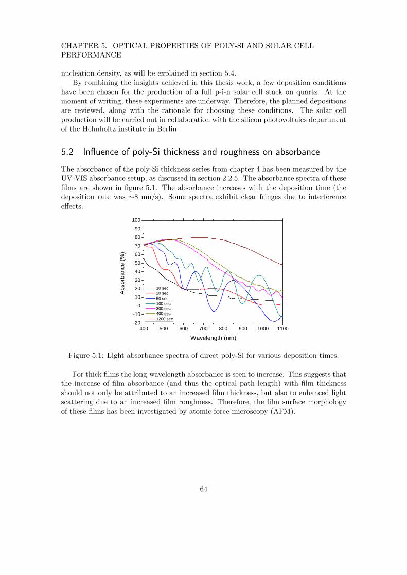
CHAPTER 5. OPTICAL PROPERTIES OF POLY-SI AND SOLAR CELLPERFORMANCE
nucleation density, as will be explained in section 5.4.By combining the insights achieved in this thesis work, a few deposition conditions
have been chosen for the production of a full p-i-n solar cell stack on quartz. At themoment of writing, these experiments are underway. Therefore, the planned depositionsare reviewed, along with the rationale for choosing these conditions. The solar cellproduction will be carried out in collaboration with the silicon photovoltaics departmentof the Helmholtz institute in Berlin.
5.2 Influence of poly-Si thickness and roughness on absorbance
The absorbance of the poly-Si thickness series from chapter 4 has been measured by theUV-VIS absorbance setup, as discussed in section 2.2.5. The absorbance spectra of thesefilms are shown in figure 5.1. The absorbance increases with the deposition time (thedeposition rate was ∼8 nm/s). Some spectra exhibit clear fringes due to interferenceeffects.
4 0 0 5 0 0 6 0 0 7 0 0 8 0 0 9 0 0 1 0 0 0 1 1 0 0- 2 0- 1 0
01 02 03 04 05 06 07 08 09 0
1 0 0
Abso
rbanc
e (%)
W a v e l e n g t h ( n m )
1 0 s e c 2 0 s e c 5 0 s e c 1 0 0 s e c 3 0 0 s e c 4 0 0 s e c 1 2 0 0 s e c
Figure 5.1: Light absorbance spectra of direct poly-Si for various deposition times.
For thick films the long-wavelength absorbance is seen to increase. This suggests thatthe increase of film absorbance (and thus the optical path length) with film thicknessshould not only be attributed to an increased film thickness, but also to enhanced lightscattering due to an increased film roughness. Therefore, the film surface morphologyof these films has been investigated by atomic force microscopy (AFM).
64
10 seconds 20 seconds
50 seconds 100 seconds
300 seconds 1200 seconds
Table 5.1: 10x10 µm2 AFM scans, showing the evolution of surface morphology fordifferent deposition times.
CHAPTER 5. OPTICAL PROPERTIES OF POLY-SI AND SOLAR CELLPERFORMANCE
AFM images of the film surface morphology for various deposition times are shownin table 5.1. With increasing deposition time the film morphology is seen to evolve froma smooth surface to a surface with a clearly visible crystal grain structure. The decreasein grain density with film thickness suggests a competition in grain growth. Also, forten seconds of deposition the film is very smooth and no surface grains are observed,even though the film is fully crystalline. After twenty seconds of deposition the scandoes show grains, which indicates that surface crystal nucleation takes place in betweenthese two deposition times. This is in line with the in-situ SE results of the previouschapter, where nucleation was observed after 17 seconds of deposition.
This decrease in grain density with film thickness has been quantified by determiningthe grain density from the AFM data. The resulting grain densities of this thickness seriesare shown in figure 5.2. After an initial jump in grain density due to the nucleation event,the grain density reduces drastically due to competitive growth. This also demonstratesthat the growth is not purely columnar, since in that case no decrease in grain densitywith film thickness would be observed. The effective average surface grain size of thesefilms is also displayed, as was calculated by taking the square root of the reciprocal graindensity.
- 1 0 1 2 3 4 5 6 7 8 9 1 0
0
2 0
4 0
6 0
8 0
1 0 0
F i l m t h i c k n e s s ( µm )
Grain
dens
ity (10
12 m
-2 )
1 0 0
2 0 0
3 0 0
4 0 0
5 0 0
6 0 0
Average grain size (nm)
Figure 5.2: The crystal grain density as a function of film thickness as obtained fromAFM measurements. The average grain size is also displayed.
The RMS surface roughness of these films is reported in figure 5.3. The film roughnessis seen to increase near-linearly with deposition time. Between ten and twenty seconds,the nucleation event is visible as the slope of the surface roughness changes.
To facilitate an easier comparison of the absorbance of these films, their absorbancehas been quantified by calculating the theoretical maximum short circuit current density(Jsc) upon AM1.5 illumination1. This has been done under the assumption that eachphoton in the wavelength range of 450-1100 nm leads to one extracted charge carrier
1A datasheet containing the AM1.5 spectrum has been obtained from the NREL website(http://rredc.nrel.gov/solar/spectra/am1.5/).
66
CHAPTER 5. OPTICAL PROPERTIES OF POLY-SI AND SOLAR CELLPERFORMANCE
0 200 400 600 800 1000 1200
0
10
20
30
40
50
60
RM
S R
ou
gh
ne
ss (
nm
)
Deposition time (s)
Figure 5.3: RMS roughness of a poly-Si thickness series as determined by AFM. The reddotted line is a guide to the eye.
(i.e. an internal quantum efficiency of 1). The wavelength of 450 nm was taken as thelower limit since this is the cut-off for the quartz substrate, and 1100 nm was taken asthe upper limit as this corresponds to the bandgap energy of c-Si. The mathematicalprocedure used for the calculation of Jsc is shown in the inset.
Mathematical procedure for determining Jsc
For the determination of Jsc it is desired to count the photons that are absorbedper second. The AM1.5 spectrum is in the form of a spectral intensity, havingthe dimension [W/m2nm]. This has been converted to a spectral photon flux bydividing by the photon energy:
Φ(λ) =I(λ)
E(λ)=I(λ)× λ
hc
[#photons
m2 × s× nm
](5.1)
The total Jsc originating from photons in the 450-1100 nm range is obtained byintegration of the product of spectral photon flux, absorbance and the elemen-tary charge e:
Jsc =
∫ 1100
450Φ(λ)×A(λ)× e dλ
[I
m2
](5.2)
In our case, this integral has been replaced by a numerical sum.
67
CHAPTER 5. OPTICAL PROPERTIES OF POLY-SI AND SOLAR CELLPERFORMANCE
The calculated Jsc values versus the film thickness, accompanied by the RMS rough-ness are displayed in figure 5.4.
100 1000 10000
0
5
10
15
20
25
30
57.6 nm
23.5 nm
19.6 nm
8.7 nm
6.0 nm4.9 nmM
axim
um
Jsc (
mA
/cm
2)
Film thickness (nm)
1.9 nm
CSG Solar (SPC)
Kaneka corporation (direct)
Osaka university (direct)
W. Schottky institute (R-ALILE)
IMEC (AIC)
Figure 5.4: Maximum short circuit current density as calculated from the measuredabsorbance curves, along with the RMS roughness of these films. For comparison, thebest-performing poly-Si solar cells mentioned in the introduction are indicated in thegraph.
The maximum short circuit current density is seen to increase with film thickness, incorrespondence with the observed increase of spectral absorbance with increasing filmthickness in figure 5.1. As indicated by the blue dotted line in figure 5.4, the maximumJsc increases logarithmically with the film thickness for the three thinnest films. This isin line with Lambert-Beer’s law, which states that light intensity shows an exponentialdecay in an absorbing medium. However, the thicker and rougher films deviate fromthis trend, as shown by the red dotted line. It is thought that the additional absorbance(and thus higher Jsc) of these films originates from the increased optical light path dueto scattering at the rough surface.
The best-performing poly-Si solar cells, as mentioned in the introduction, are indi-cated in the graph. As can be seen, the theoretical maximum Jsc of the ETP-depositedpoly-Si is in all cases lower than the experimentally reported values, even though aninternal quantum efficiency of 1 was assumed. However, it should be noted that theabsorbance measurements are done on bare poly-Si on quartz, whereas the processed so-lar cells make use of additional light trapping techniques like a backreflector and roughsubstrates.
5.3 Absorbance of SPC poly-Si films of varying roughness
Unfortunately, although the results shown above indicate a beneficial effect of surfaceroughness on the absorbance for our films, the effect of film roughness and thickness
68
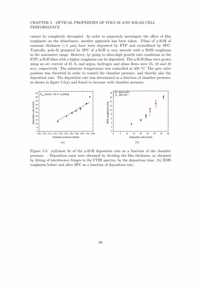
CHAPTER 5. OPTICAL PROPERTIES OF POLY-SI AND SOLAR CELLPERFORMANCE
cannot be completely decoupled. In order to separately investigate the effect of filmroughness on the absorbance, another approach has been taken. Films of a-Si:H ofconstant thickness (∼1 µm) have been deposited by ETP and crystallized by SPC.Typically, poly-Si prepared by SPC of a-Si:H is very smooth with a RMS roughnessin the nanometer range. However, by going to ultra-high growth rate conditions in theETP, a-Si:H films with a higher roughness can be deposited. The a-Si:H films were grownusing an arc current of 45 A, and argon, hydrogen and silane flows were 55, 10 and 10sccs, respectively. The substrate temperature was controlled at 450 oC. The gate valveposition was throttled in order to control the chamber pressure, and thereby also thedeposition rate. The deposition rate was determined as a function of chamber pressure,as shown in figure 5.5(a) and found to increase with chamber pressure.
0 . 0 0 0 . 0 5 0 . 1 0 0 . 1 5 0 . 2 0 0 . 2 5 0 . 3 0 0 . 3 5 0 . 4 0 0 . 4 5 0 . 5 005
1 01 52 02 53 03 54 04 55 0
Depo
sition
rate
(nm/s)
C h a m b e r p r e s s u r e ( m b a r )
R d e p [ n m / s ] = 8 1 . 3 * p [ m b a r ]
(a)
0 5 1 0 1 5 2 0 2 5 3 0 3 5 4 002468
1 01 21 41 61 8
B e f o r e S P C A f t e r S P C
RMS r
ough
ness
(nm)
D e p o s i t i o n r a t e ( n m / s )(b)
Figure 5.5: (a)Linear fit of the a-Si:H deposition rate as a function of the chamberpressure. . Deposition rates were obtained by dividing the film thickness, as obtainedby fitting of interference fringes in the FTIR spectra, by the deposition time. (b) RMSroughness before and after SPC as a function of deposition rate.
69
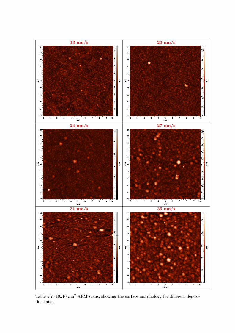
13 nm/s 20 nm/s
24 nm/s 27 nm/s
31 nm/s 36 nm/s
Table 5.2: 10x10 µm2 AFM scans, showing the surface morphology for different deposi-tion rates.
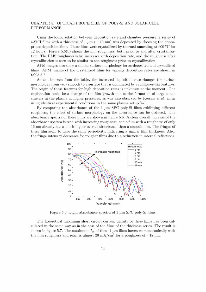
CHAPTER 5. OPTICAL PROPERTIES OF POLY-SI AND SOLAR CELLPERFORMANCE
Using the found relation between deposition rate and chamber pressure, a series ofa-Si:H films with a thickness of 1 µm (± 10 nm) was deposited by choosing the appro-priate deposition time. These films were crystallized by thermal annealing at 600 oC for12 hours. Figure 5.5(b) shows the film roughness, both prior to and after crystalliza-tion. The RMS roughness value increases with deposition rate, and the roughness aftercrystallization is seen to be similar to the roughness prior to crystallization.
AFM images also show a similar surface morphology for as-deposited and crystallizedfilms. AFM images of the crystallized films for varying deposition rates are shown intable 5.2.
As can be seen from the table, the increased deposition rate changes the surfacemorphology from very smooth to a surface that is dominated by cauliflower-like features.The origin of these features for high deposition rates is unknown at the moment. Oneexplanation could be a change of the film growth due to the formation of large silaneclusters in the plasma at higher pressures, as was also observed by Kessels et al. whenusing identical experimental conditions in the same plasma setup.[47]
By comparing the absorbance of the 1 µm SPC poly-Si films exhibiting differentroughness, the effect of surface morphology on the absorbance can be deduced. Theabsorbance spectra of these films are shown in figure 5.6. A clear overall increase of theabsorbance spectra is seen with increasing roughness, and a film with a roughness of only16 nm already has a much higher overall absorbance than a smooth film. The fringes ofthese film seem to have the same periodicity, indicating a similar film thickness. Also,the fringe intensity decreases for rougher films due to a reduction in internal reflections.
5 0 0 6 0 0 7 0 0 8 0 0 9 0 0 1 0 0 0 1 1 0 00
1 02 03 04 05 06 07 08 09 0
1 0 0
Abso
rbanc
e (%)
W a v e l e n g t h ( n m )
R o u g h n e s s : 3 n m 5 n m 7 n m 9 n m 1 3 n m 1 6 n m
I n c r e a s i n g r o u g h n e s s
Figure 5.6: Light absorbance spectra of 1 µm SPC poly-Si films.
The theoretical maximum short circuit current density of these films has been cal-culated in the same way as in the case of the films of the thickness series. The result isshown in figure 5.7. The maximum Jsc of these 1 µm films increases monotonically withthe film roughness and reaches almost 20 mA/cm2 for a roughness of ∼18 nm.
71
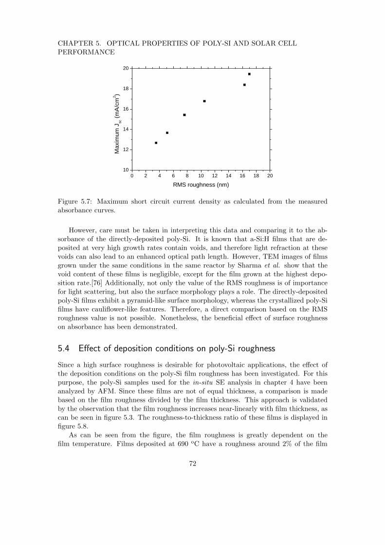
CHAPTER 5. OPTICAL PROPERTIES OF POLY-SI AND SOLAR CELLPERFORMANCE
0 2 4 6 8 1 0 1 2 1 4 1 6 1 8 2 01 0
1 2
1 4
1 6
1 8
2 0
Maxim
um J sc (m
A/cm2 )
R M S r o u g h n e s s ( n m )
Figure 5.7: Maximum short circuit current density as calculated from the measuredabsorbance curves.
However, care must be taken in interpreting this data and comparing it to the ab-sorbance of the directly-deposited poly-Si. It is known that a-Si:H films that are de-posited at very high growth rates contain voids, and therefore light refraction at thesevoids can also lead to an enhanced optical path length. However, TEM images of filmsgrown under the same conditions in the same reactor by Sharma et al. show that thevoid content of these films is negligible, except for the film grown at the highest depo-sition rate.[76] Additionally, not only the value of the RMS roughness is of importancefor light scattering, but also the surface morphology plays a role. The directly-depositedpoly-Si films exhibit a pyramid-like surface morphology, whereas the crystallized poly-Sifilms have cauliflower-like features. Therefore, a direct comparison based on the RMSroughness value is not possible. Nonetheless, the beneficial effect of surface roughnesson absorbance has been demonstrated.
5.4 Effect of deposition conditions on poly-Si roughness
Since a high surface roughness is desirable for photovoltaic applications, the effect ofthe deposition conditions on the poly-Si film roughness has been investigated. For thispurpose, the poly-Si samples used for the in-situ SE analysis in chapter 4 have beenanalyzed by AFM. Since these films are not of equal thickness, a comparison is madebased on the film roughness divided by the film thickness. This approach is validatedby the observation that the film roughness increases near-linearly with film thickness, ascan be seen in figure 5.3. The roughness-to-thickness ratio of these films is displayed infigure 5.8.
As can be seen from the figure, the film roughness is greatly dependent on thefilm temperature. Films deposited at 690 oC have a roughness around 2% of the film
72
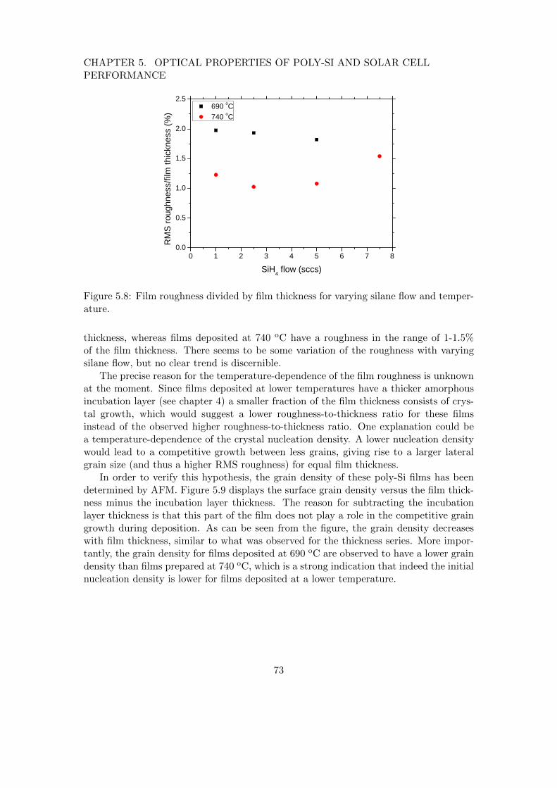
CHAPTER 5. OPTICAL PROPERTIES OF POLY-SI AND SOLAR CELLPERFORMANCE
0 1 2 3 4 5 6 7 80 . 0
0 . 5
1 . 0
1 . 5
2 . 0
2 . 5 6 9 0 o C 7 4 0 o C
RMS r
ough
ness/
film th
ickne
ss (%
)
S i H 4 f l o w ( s c c s )
Figure 5.8: Film roughness divided by film thickness for varying silane flow and temper-ature.
thickness, whereas films deposited at 740 oC have a roughness in the range of 1-1.5%of the film thickness. There seems to be some variation of the roughness with varyingsilane flow, but no clear trend is discernible.
The precise reason for the temperature-dependence of the film roughness is unknownat the moment. Since films deposited at lower temperatures have a thicker amorphousincubation layer (see chapter 4) a smaller fraction of the film thickness consists of crys-tal growth, which would suggest a lower roughness-to-thickness ratio for these filmsinstead of the observed higher roughness-to-thickness ratio. One explanation could bea temperature-dependence of the crystal nucleation density. A lower nucleation densitywould lead to a competitive growth between less grains, giving rise to a larger lateralgrain size (and thus a higher RMS roughness) for equal film thickness.
In order to verify this hypothesis, the grain density of these poly-Si films has beendetermined by AFM. Figure 5.9 displays the surface grain density versus the film thick-ness minus the incubation layer thickness. The reason for subtracting the incubationlayer thickness is that this part of the film does not play a role in the competitive graingrowth during deposition. As can be seen from the figure, the grain density decreaseswith film thickness, similar to what was observed for the thickness series. More impor-tantly, the grain density for films deposited at 690 oC are observed to have a lower graindensity than films prepared at 740 oC, which is a strong indication that indeed the initialnucleation density is lower for films deposited at a lower temperature.
73
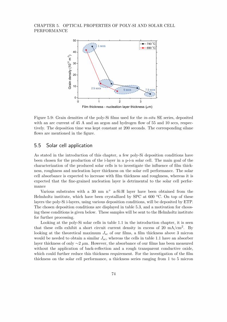
CHAPTER 5. OPTICAL PROPERTIES OF POLY-SI AND SOLAR CELLPERFORMANCE
0 1 2 3
0
10
20
30
40
50
Gra
in d
en
sity (
10
12 m
-2)
Film thickness - nucleation layer thickness (m)
740 oC
690 oC
1 sccs
2.5 sccs 5 sccs 7.5 sccs
Figure 5.9: Grain densities of the poly-Si films used for the in-situ SE series, depositedwith an arc current of 45 A and an argon and hydrogen flow of 55 and 10 sccs, respec-tively. The deposition time was kept constant at 200 seconds. The corresponding silaneflows are mentioned in the figure.
5.5 Solar cell application
As stated in the introduction of this chapter, a few poly-Si deposition conditions havebeen chosen for the production of the i-layer in a p-i-n solar cell. The main goal of thecharacterization of the produced solar cells is to investigate the influence of film thick-ness, roughness and nucleation layer thickness on the solar cell performance. The solarcell absorbance is expected to increase with film thickness and roughness, whereas it isexpected that the fine-grained nucleation layer is detrimental to the solar cell perfor-mance
Various substrates with a 30 nm n+ a-Si:H layer have been obtained from theHelmholtz institute, which have been crystallized by SPC at 600 oC. On top of theselayers the poly-Si i-layers, using various deposition conditions, will be deposited by ETP.The chosen deposition conditions are displayed in table 5.3, and a motivation for choos-ing these conditions is given below. These samples will be sent to the Helmholtz institutefor further processing.
Looking at the poly-Si solar cells in table 1.1 in the introduction chapter, it is seenthat these cells exhibit a short circuit current density in excess of 20 mA/cm2. Bylooking at the theoretical maximum Jsc of our films, a film thickness above 3 micronwould be needed to obtain a similar Jsc, whereas the cells in table 1.1 have an absorberlayer thickness of only ∼2 µm. However, the absorbance of our films has been measuredwithout the application of back-reflection and a rough transparent conductive oxide,which could further reduce this thickness requirement. For the investigation of the filmthickness on the solar cell performance, a thickness series ranging from 1 to 5 micron
74

CHAPTER 5. OPTICAL PROPERTIES OF POLY-SI AND SOLAR CELLPERFORMANCE
Sample H2 flow SiH4 flow Temperature Thickness(sccs) (sccs) (oC (nm)
Berlin01 10 2.5 740 1000Berlin02 10 2.5 740 2500Berlin03 10 2.5 740 5000Berlin04 10 2.5 690 1000Berlin05 10 2.5 690 2500Berlin06 30 2.5 740 2500Berlin07 10 7.5 740 2500
Table 5.3: Overview of the deposition conditions for the poly-Si i-layer for applicationin a p-i-n solar cell stack.
will be deposited at our standard condition (samples Berlin01-Berlin03).Two samples (Berlin04 and Berlin05) of 1 and 2.5 micron will be deposited at a
lower temperature of 690 oC. The lower temperature will lead to a higher roughness andthicker nucleation layer. By comparing these two samples to Berlin01 and Berlin02, theeffect of deposition temperature on solar cell performance can be deduced.
Sample Berlin06 has the same deposition conditions as sample Berlin02, except forthe higher hydrogen flow of 30 sccs. It is known from the in-situ SE study that theamorphous-crystalline transition occurs earlier for this higher hydrogen flow. Since thesetwo conditions also have a similar roughness-to-thickness ratio, it is thought that acomparison between these two samples can elucidate the effect of the nucleation layeron the solar cell performance.
Finally, one sample will be deposited at a higher silane flow of 7.5 sccs. This conditionhas been chosen to see whether an acceptable solar cell performance can be obtained ata high deposition rate close to 20 nm/s.
5.6 Conclusions
In this chapter, the correlation between film thickness, surface morphology and ab-sorbance has been investigated. UV-VIS absorbance measurements on a thickness seriesof directly-deposited poly-Si revealed an increase in absorbance for thicker films, es-pecially in the long-wavelength region. AFM showed a near-linear increase of RMSroughness with film thickness, which has been attributed to crystal growth. The theo-retical maximum Jsc of these films under AM1.5 illumination has been calculated fromthe measured absorbance curves. For thin films (≤400 nm) with a low roughness, thefilm absorbance increases logarithmically with the film thickness, which is in line withLambert-Beer’s law. However, for thicker films a steeper increase of absorbance withthickness was observed. Scattering at the rough interface has been assigned as the reasonfor this increased absorbance.
To decouple the effect of surface roughness on the film absorbance from the film
75

CHAPTER 5. OPTICAL PROPERTIES OF POLY-SI AND SOLAR CELLPERFORMANCE
thickness, a series of 1 µm SPC poly-Si samples with a roughness varying between 3 and16 nm was deposited. A clear increase of film absorbance with roughness was observed.Unfortunately, a direct comparison with the directly-deposited poly-Si films could notbe made due to the different surface morphology.
Since a high surface roughness is beneficial for current generation in a solar cell, theeffect of deposition parameters on roughness was determined. It was found that thesurface temperature plays a decisive role in the roughness, with films deposited at 690oChaving a roughness around 2% of the film thickness, whereas films deposited at 740 oChave a roughness in the range of 1-1.5% of the film thickness.
By combining the knowledge on the dependence of the film grain morphology andabsorbance characteristics gained in this and the previous chapters, a few deposition con-ditions were chosen to deposit a poly-Si i-layer for a p-i-n solar cell stack. Unfortunately,results on solar cell performance are still underway.
76
Chapter 6
Conclusion and Outlook
In this thesis, the deposition of poly-Si thin films by an expanding thermal plasma hasbeen investigated. More specifically, three main research topics have been addressed, asstated in the introduction:
• Is it possible to deposit poly-Si with an expanding thermal plasma?
• How do crystal grains develop during deposition?
• In view of solar cell applications, what are the optical properties of ETP-depositedpoly-Si films?
These topics have been treated in chapters 3-5. The main conclusions drawn in thesechapters are summarized in the sections below.
6.1 The feasibility of depositing poly-Si by ETP
In order to investigate the feasibility of depositing poly-Si by an expanding thermalplasma, two routes have been taken. The first route consisted of a pulsed deposition,where the silane gas flow in an Ar-H2-SiH4 plasma is pulsed. This was carried out inorder to alternate deposition with a hydrogen plasma treatment, which is thought toaid in film crystallization. However, it was found that for silane ’off-times’ above thechamber residence time the film crystallinity decreased due to the hydrogen treatment.
Although the precise reason for this unexpected trend is not known, various possiblereasons have been proposed. Among these are a too high deposition thickness per pulse,which prevents hydrogen induced crystallization, a varying amount of SiH4 per pulsefor different off-times, which changes the plasma chemistry and finally the possibilitythat the hydrogen radical and ion fluxes/energies in the ETP setup are not suitable forcrystallization. The use of in-situ techniques to monitor the film properties like SE andATR-FTIR could be of great help to gain further understanding in this respect.
The second approach was a high-temperature route, as it was found that a substratetemperature of∼800 oC is needed for direct poly-Si deposition. By varying the deposition
77
CHAPTER 6. CONCLUSION AND OUTLOOK
conditions and monitoring the plasma by OES, it was found that the film phase iscritically dependent on the growth precursors.
In short, it was found that SiH3 dominated growth, in combination with a sufficientatomic hydrogen flux results in the deposition of good quality poly-Si. Depositionswithout hydrogen admixed in the arc result in amorphous films, which is thought tooriginate from a lack of H flux towards the surface and from the very sticky SiHx (x≤2)growth radicals. Films deposited at high H2/SiH4 dilution ratios were found to becrystalline but porous, which is attributed to the low surface diffusivity of sticky SiHx
(x≤2) growth radicals. At very low dilution ratios films are found to be amorphous,which is attributed to a depletion of the atomic hydrogen by the silane. A good qualitypoly-Si film was deposited at an intermediate dilution ratio (R=4).
This film initial poly-Si film was found to have an inhomogeneous grain morphology,with small grains at the bottom of the film, evolving into a columnar grain morphology.The film exhibits a self-structured pyramid-like surface morphology and has a preferential(220) orientation. A high unoptimized deposition rate of 8 nm/s was achieved.
6.2 Crystal growth in ETP-deposited poly-Si
In chapter 4, the crystal growth was investigated more in detail by a combination of in-situ SE and ex-situ XRD on a thickness series. Based on the observations, the followinggrowth model was proposed. Film growth is initially amorphous, as observed by in-situSE. After a certain incubation layer thickness, structural relaxation of the surface takesplace, which has a corresponding dip in the surface roughness and a transition fromamorphous to crystalline growth. From this thickness, crystals grow in a preferential(220) direction, as observed by XRD. Due to the high deposition temperature, solid phasecrystallization of the amorphous incubation layer takes place, leading to the formationof small (≤100 nm) randomly oriented grains in the incubation layer. This growthmodel has been verified by TEM, which shows a clear transition between randomlyoriented small grains in the incubation layer to columnar (220) growth. Therefore, novelinsights in the evolution of crystal growth in ETP-deposited poly-Si have been gained.Additionally, these insights might not only be applicable to ETP, but also to otherhigh-temperature poly-Si deposition techniques where SPC of the amorphous incubationlayer can play a role. It is also important to stress that these novel insights were onlyobtainable thanks to the use of in-situ techniques, which revealed a dynamic behaviour(i.e. SPC of the incubation layer), a process which could have never been observed byex-situ techniques.
Furthermore, it was found that the incubation layer thickness is highly dependenton the substrate temperature and growth precursors. A high substrate temperatureand hydrogen flow promote the transition, whereas a high SiH4 flow (and thus a highdeposition rate) leads to a thicker incubation layer. To conclude, despite the presence ofan incubation layer, it has been demonstrated that the ETP is capable of depositing poly-Si at a high deposition rate (up to 20 nm/s) and with the beneficial (220) orientation.An interesting follow-up research topic would be to investigate the effect of substrate
78
CHAPTER 6. CONCLUSION AND OUTLOOK
biasing, which could potentially reduce the required deposition temperature.
6.3 Optical properties of poly-Si and its application in solar cells
In the final chapter, the effect of film thickness and surface morphology on absorbancewas investigated. By comparing the absorbance of a thickness series of direct poly-Si, itwas found that the film absorbance increases super-logarithmically with thickness, whichis attributed to the rough pyramid-like surface morphology for thicker films.
The absorbance of a series of 1 µm SPC poly-Si films of varying roughness was mea-sured in order to decouple the effect of film roughness from the thickness on absorbance.The overall absorbance was found to almost double when going from a film with 3 nmroughness to a film with 18 nm of roughness, demonstrating the beneficial effect of sur-face roughness on light trapping. Unfortunately, a one-to-one comparison with directpoly-Si cannot be made, due to a different surface morphology.
For directly-deposited poly-Si, it was found that the substrate temperature has amajor influence of the film roughness. For a deposition temperature of 740 oC, the filmroughness/thickness ratio is ∼1-1.5%, whereas it is ∼ 2% for films deposited at 690 oC.An increase in nucleation density with increasing substrate temperature was put forwardas a possible explanation for this observation.
Some deposition conditions have been chosen for processing in a full p-i-n solar cellstack in collaboration with the Helmholtz institute in Berlin, but no results are availableat the time of writing.
79
Acknowledgments
In this section, I would like to thank the people that have been important to me duringthis graduation project, both scientifically and personally.
To start with, I would like to deeply express my gratitude to the technicians of theP&MP group: Joris Meulendijks, Cristian van Helvoirt, Janneke Zeebregts and Ries vande Sande. Without their expertise and enthusiasm, I could not have achieved the resultspresented in this thesis. Especially Ries is thanked for his extensive help on the heater,even though it broke down so many times. I wish you all the best for your retirement,which will be a great loss to the P&MP group.
Secondly, I would like to thank Jan-Willem Weber for his great contribution in settingup the spectroscopic ellipsometry measurements (together with Gianfranco Aresta). Notonly did you encourage me to do in-situ SE, your deep understanding of the SE techniquealso proved of great value for the data analysis!
Great thanks go to Wytze Keuning and Marcel Verheijen for making lamella’s forthe TEM scan and performing the TEM scan, respectively. Marcel, you are thankedfor the fruitful discussion of the TEM result. Wytze, you are also deeply thanked forfruitful discussions on XRD results, making SEM images and for performing HF-dips.Your expertise on all the instruments of P&MP makes you invaluable to the group.
Kashish, special thanks go to you. Not only for being my daily supervisor, but alsofor being a good friend. We have worked together for a few years now, and I think it issafe to say we make a mean team!
Adriana, I think most of my thanks should go to you. We met three years ago for anOGO project, and since then I stayed at P&MP as an AFM operator, did my bachelorproject, my internship in Colorado and my graduation project, all under your guidance.You arranged our internship in Colorado, where I had the time of my life, and for thatI am very grateful.
I would also like to thank the students in the student room for making the studentroom not only a place to work, but also for the occasional laugh! Especially Bas, Nickand Rene, with whom I’ve spent my time in Colorado, you have proven to be greatfriends and we share many great memories.
Erwin, you are thanked for providing me with the bible of depo II, which is yourPhD thesis. It has provided me with the knowledge of the system I needed to performthe research in this thesis. Additionally, I am very grateful for the PhD position onheterojunction solar cells you have offered me.
80

CHAPTER 6. CONCLUSION AND OUTLOOK
I would of course also like to thank my family and my girlfriend Cherelle. Youprovided me with a warm home and everything I needed to work on my graduationproject, for which I’m very grateful. This year hasn’t been the easiest, especially withmy father fighting cancer. Dad, I’m very happy you recovered!
To end with, I would like to say that I’ve really enjoyed my years at P&MP! Thegroup spirit is great, and I’ve made many friends over the years. Fortunately, I will stayfor another four years in this group for a PhD position, working on a new challenge. Soluckily I will not have to miss out on the almost daily ’vlaai’, the weekly Borrel, theyearly football tournament and the great PhD graduation parties!
81
Appendix A
Determination of radical fluxes
A.1 Calculation of silyl flux
As stated in section 3.3, it is plausible that during high-temperature poly-Si depositionthe silyl radicals have a sticking coefficient close to unity, most likely due to a veryreactive hydrogen-deficient surface. Using this notion, together with the experimentallydetermined deposition rate of 8 nm/s, it is possible to make an estimate for the flux ofsilyl radicals (which is mostly SiH3) at our standard condition (55 sccs argon, 10 sccshydrogen, 2.5 sccs silane).
Since every impinging silyl radical contributes to growth, the growth flux is equal tothe silicon atomic density times the deposition rate:
Φ = nSi ×Rdep (A.1)
The atomic density of silicon can be calculated from the lattice constant a, which is5.431 A and the fact that in the diamond lattice of c-Si there are 8 atoms per unit cell
nSi =8 atoms
a3= 5× 1028 m−3 (A.2)
The growth flux is then:
Φ = nSi ×Rdep = 5× 1028 × 8× 10−9 = 4× 10²⁰atoms
m2s(A.3)
Kessels et al. have experimentally determined this growth flux to be 3× 10²⁰ atomsm2s
under identical conditions on the same plasma setup.[47] The fact that a very similarvalue is obtained by assuming a sticking coefficient of unity justifies this approach.
A.2 Approximating the flux ratio
In this section, it is attempted to get an estimate on the SiH3/H arrival ratio at thesubstrate holder. This will be done using a number of assumptions and simplifications.
82
APPENDIX A. DETERMINATION OF RADICAL FLUXES
Therefore, the resulting ratio should be considered as a indication for the order of mag-nitude of the SiH3/H arrival ratio and not as the exact value.
The SiH3/H arrival ratio will be calculated for the conditions used for the in-situ SEseries. (55 sccs of argon, 10 sccs of hydrogen and 1-7.5 sccs of SiH4). Fortunately, theSiH3 densities for these conditions have been determined experimentally by Kessels etal. and are used as an input for the calculations.[47]
However, the atomic hydrogen flux towards the substrate holder under these condi-tions should also be known for the calculation of the SiH3/H arrival ratio. The atomichydrogen density in front of the substrate holder under these conditions is only knownfor a silane flow of 0 and 10 sccs. For no silane flow, the hydrogen density is ∼ 5× 10¹⁷
m−3.[46] For a silane flow of 10 sccs, the hydrogen density has been estimated frommodeling work by Kessels at al. to be ∼ 4× 10¹⁶ m−3.[77]
The atomic hydrogen density as a function of silane flow has been estimated using theassumption that an increase in SiH3 density with silane flow corresponds to a decreasein atomic H density due to the hydrogen abstraction reaction:
SiH4 +H → SiH3 +H2 (A.4)
With this assumption, the atomic H density as a function of SiH3 density has beencalculated by:
nH(nSiH3) = nH (SiH4=0) −nSiH3
nSiH3 (SiH4=10)
× (nH (SiH4=0) − nH (SiH4=10)) (A.5)
In this equation, the known input parameters are:
• nH (SiH4=0), the atomic hydrogen density when no silane is injected (5×10¹⁷ m−3)
• nSiH3 (SiH4=10), the SiH3 density for a silane flow of 10 sccs (3× 10¹⁸ m−3)
• nH (SiH4=10), the atomic hydrogen density for a silane flow of 10 sccs ( ∼ 4× 10¹⁶
m−3)
The experimentally determined SiH3 densities, along with the calculated hydrogendensities are shown in figure A.1
From these densities, the SiH3/H arrival ratio can be calculated. It is assumed thatthe fluxes can be obtained from the simple relation:
Φ =nv
4(A.6)
Which is only valid for a Maxwellian distribution and completely neglects the pres-ence of any flow fields. The SiH3/H arrival ratio is the ratio of the fluxes, i.e.:
Ratio =nSiH3
nH× vHvSiH3
=nSiH3
nH× 1√
(31)(A.7)
83
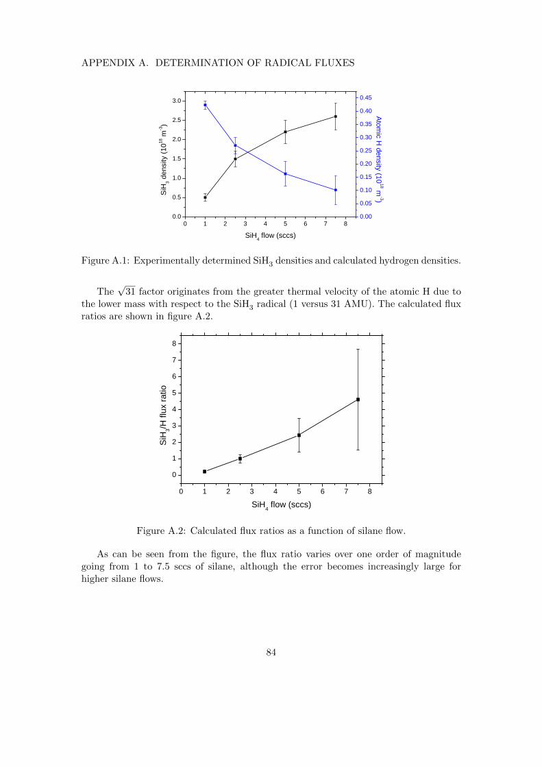
APPENDIX A. DETERMINATION OF RADICAL FLUXES
0 1 2 3 4 5 6 7 80 . 0
0 . 5
1 . 0
1 . 5
2 . 0
2 . 5
3 . 0
S i H 4 f l o w ( s c c s )
SiH3 de
nsity
(1018
m-3 )
0 . 0 00 . 0 50 . 1 00 . 1 50 . 2 00 . 2 50 . 3 00 . 3 50 . 4 00 . 4 5
Atomic H density (10 18 m-3)
Figure A.1: Experimentally determined SiH3 densities and calculated hydrogen densities.
The√
31 factor originates from the greater thermal velocity of the atomic H due tothe lower mass with respect to the SiH3 radical (1 versus 31 AMU). The calculated fluxratios are shown in figure A.2.
0 1 2 3 4 5 6 7 8012345678
SiH3/H
flux r
atio
S i H 4 f l o w ( s c c s )
Figure A.2: Calculated flux ratios as a function of silane flow.
As can be seen from the figure, the flux ratio varies over one order of magnitudegoing from 1 to 7.5 sccs of silane, although the error becomes increasingly large forhigher silane flows.
84
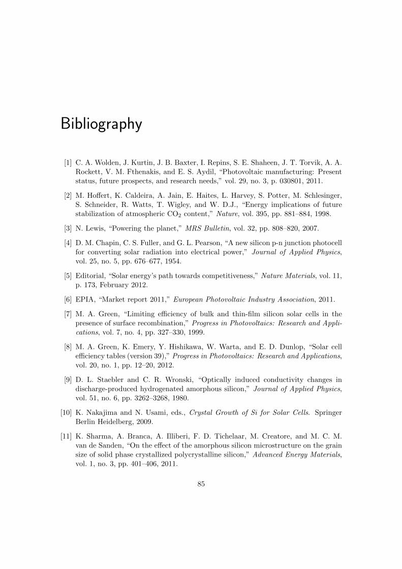
Bibliography
[1] C. A. Wolden, J. Kurtin, J. B. Baxter, I. Repins, S. E. Shaheen, J. T. Torvik, A. A.Rockett, V. M. Fthenakis, and E. S. Aydil, “Photovoltaic manufacturing: Presentstatus, future prospects, and research needs,” vol. 29, no. 3, p. 030801, 2011.
[2] M. Hoffert, K. Caldeira, A. Jain, E. Haites, L. Harvey, S. Potter, M. Schlesinger,S. Schneider, R. Watts, T. Wigley, and W. D.J., “Energy implications of futurestabilization of atmospheric CO2 content,” Nature, vol. 395, pp. 881–884, 1998.
[3] N. Lewis, “Powering the planet,” MRS Bulletin, vol. 32, pp. 808–820, 2007.
[4] D. M. Chapin, C. S. Fuller, and G. L. Pearson, “A new silicon p-n junction photocellfor converting solar radiation into electrical power,” Journal of Applied Physics,vol. 25, no. 5, pp. 676–677, 1954.
[5] Editorial, “Solar energy’s path towards competitiveness,” Nature Materials, vol. 11,p. 173, February 2012.
[6] EPIA, “Market report 2011,” European Photovoltaic Industry Association, 2011.
[7] M. A. Green, “Limiting efficiency of bulk and thin-film silicon solar cells in thepresence of surface recombination,” Progress in Photovoltaics: Research and Appli-cations, vol. 7, no. 4, pp. 327–330, 1999.
[8] M. A. Green, K. Emery, Y. Hishikawa, W. Warta, and E. D. Dunlop, “Solar cellefficiency tables (version 39),” Progress in Photovoltaics: Research and Applications,vol. 20, no. 1, pp. 12–20, 2012.
[9] D. L. Staebler and C. R. Wronski, “Optically induced conductivity changes indischarge-produced hydrogenated amorphous silicon,” Journal of Applied Physics,vol. 51, no. 6, pp. 3262–3268, 1980.
[10] K. Nakajima and N. Usami, eds., Crystal Growth of Si for Solar Cells. SpringerBerlin Heidelberg, 2009.
[11] K. Sharma, A. Branca, A. Illiberi, F. D. Tichelaar, M. Creatore, and M. C. M.van de Sanden, “On the effect of the amorphous silicon microstructure on the grainsize of solid phase crystallized polycrystalline silicon,” Advanced Energy Materials,vol. 1, no. 3, pp. 401–406, 2011.
85
BIBLIOGRAPHY
[12] A. Illiberi, K. Sharma, M. Creatore, and M. van de Sanden, “Novel approach tothin film polycrystalline silicon on glass,” Materials Letters, vol. 63, no. 21, pp. 1817– 1819, 2009.
[13] M. Green, P. Basore, N. Chang, D. Clugston, R. Egan, R. Evans, D. Hogg, S. Jar-nason, M. Keevers, P. Lasswell, J. O. Sullivan, U. Schubert, A. Turner, S. Wenham,and T. Young, “Crystalline silicon on glass (CSG) thin-film solar cell modules,”Solar Energy, vol. 77, no. 6, pp. 857 – 863, 2004.
[14] J. Rath, “Low temperature polycrystalline silicon: a review on deposition, physicalproperties and solar cell applications,” Solar energy materials and solar cells, vol. 76,no. 4, pp. 431–487, 2003.
[15] S.-Y. Lien, H.-Y. Mao, B.-R. Wu, R.-H. Horng, and D.-S. Wuu, “Incubation effectsupon polycrystalline silicon on glass deposited by hot-wire cvd,” Chemical VaporDeposition, vol. 13, no. 5, pp. 247–252, 2007.
[16] C. Jaeger, T. Matsui, M. Takeuchi, M. Karasawa, M. Kondo, and M. Stutzmann,“Thin film solar cells prepared on low thermal budget polycrystalline silicon seedlayers,” Japanese Journal of Applied Physics, vol. 49, no. 11, p. 112301, 2010.
[17] I. Gordon, L. Carnel, D. Van Gestel, G. Beaucarne, and J. Poortmans, “8% efficientthin-film polycrystalline-silicon solar cells based on aluminum-induced crystalliza-tion and thermal CVD,” Progress in Photovoltaics: Research and Applications,vol. 15, no. 7, pp. 575–586, 2007.
[18] I. Gordon, L. Carnel, D. Van Gestel, G. Beaucarne, and J. Poortmans, “Fabricationand characterization of highly efficient thin-film polycrystalline-silicon solar cellsbased on aluminium-induced crystallization,” Thin Solid Films, vol. 516, no. 20,pp. 6984–6988, 2008.
[19] I. Kuzma-Filipek, F. Dross, K. Baert, J. L. Hernandez, S. Singh, K. Van Nieuwen-huysen, and J. Poortmans, “16% thin-film epitaxial silicon solar cells on 70-cm2 areawith 30-µm active layer, porous silicon back reflector, and Cu-based top-contactmetallization,” Progress in Photovoltaics: Research and Applications, 2011.
[20] J. Poortmans and V. Arkhipov, Thin Film Solar Cells: Fabrication, Characteriza-tion and Applications. Wiley Series in Materials for Electronic and OptoelectronicApplications, Wiley, 2006.
[21] K. Yamamoto, “Very thin film crystalline silicon solar cells on glass substrate fab-ricated at low temperature,” Electron Devices, IEEE Transactions on, vol. 46,pp. 2041 –2047, oct 1999.
[22] T. Matsui, M. Tsukiji, H. Saika, T. Toyama, and H. Okamoto, “Correlation be-tween microstructure and photovoltaic performance of polycrystalline silicon thinfilm solar cells,” Japanese Journal of Applied Physics, vol. 41, no. Part 1, No. 1,pp. 20–27, 2002.
86
BIBLIOGRAPHY
[23] J. Rath, R. Schropp, and W. Beyer, “Hydrogen diffusion through deformed Si-Si bonds at grain boundaries in hot-wire CVD polycrystalline silicon films,” inPolycrystalline semiconductors IV materials, technologies and large area electronics(O. Bonnaud, T. Mohammed Brahim, H. Strunk, and J. Werner, eds.), vol. 80-81of Solid State Phenomena Series, pp. 109–114, 2001. 6th International Conferenceon Polycrystalline Semiconductors, St Malo, France, Sep 03-07, 2000.
[24] K. Nakahata, T. Kamiya, C. Fortmann, I. Shimizu, H. Stuchl Kova, A. Fejfar, andJ. Ko, “Anisotropic carrier transport in preferentially oriented polycrystalline siliconfilms fabricated by very-high-frequency plasma enhanced chemical vapor depositionusing fluorinated source gas,” Journal of non-crystalline solids, vol. 266, pp. 341–346, 2000.
[25] S. Pizzini, Advanced Silicon Materials for Photovoltaic Applications. John Wiley &Sons, 2012.
[26] J. Wong, J. L. Huang, B. Eggleston, M. A. Green, O. Kunz, R. Evans, M. Keevers,and R. J. Egan, “Lifetime limiting recombination pathway in thin-film polycrys-talline silicon on glass solar cells,” vol. 107, no. 12, p. 123705, 2010.
[27] J. Wong, J. Huang, S. Varlamov, M. A. Green, and M. Keevers, “The roles ofshallow and deep levels in the recombination behavior of polycrystalline silicon onglass solar cells,” Progress in Photovoltaics: Research and Applications, 2011.
[28] J. Wong, J. L. Huang, S. Varlamov, M. A. Green, R. Evans, M. Keevers, and R. J.Egan, “Structural inhomogeneities in polycrystalline silicon on glass solar cells andtheir effects on device characteristics,” Progress in Photovoltaics: Research andApplications, vol. 19, no. 6, pp. 695–705, 2011.
[29] S. Kasap and P. Capper, Springer Handbook of Electronic And Photonic Materials.Springer Handbook of, Springer, 2006.
[30] L. Guo, M. Kondo, M. Fukawa, K. Saitoh, and A. Matsuda, “High rate deposi-tion of microcrystalline silicon using conventional plasma-enhanced chemical vapordeposition,” Japanese journal of applied physics, vol. 37, pp. L1116–L1118, 1998.
[31] M. Kondo and A. Matsuda, “Low temperature growth of microcrystalline siliconand its application to solar cells,” Thin Solid Films, vol. 383, no. 1, pp. 1–6, 2001.
[32] A. Matsuda, “Microcrystalline silicon.: Growth and device application,” Journal ofNon-Crystalline Solids, vol. 338, no. 0, pp. 1 – 12, 2004. Proceedings of the 20thInternational Conference on Amorphous and Microcrystalline Semiconductors.
[33] A. Matsuda, “Formation kinetics and control of microcrystallite in µc-Si:H fromglow discharge plasma,” Journal of Non-Crystalline Solids, no. 0, pp. 767 – 774,1983. Proceedings of the Tenth International Conference on Amorphous and LiquidSemiconductors.
87
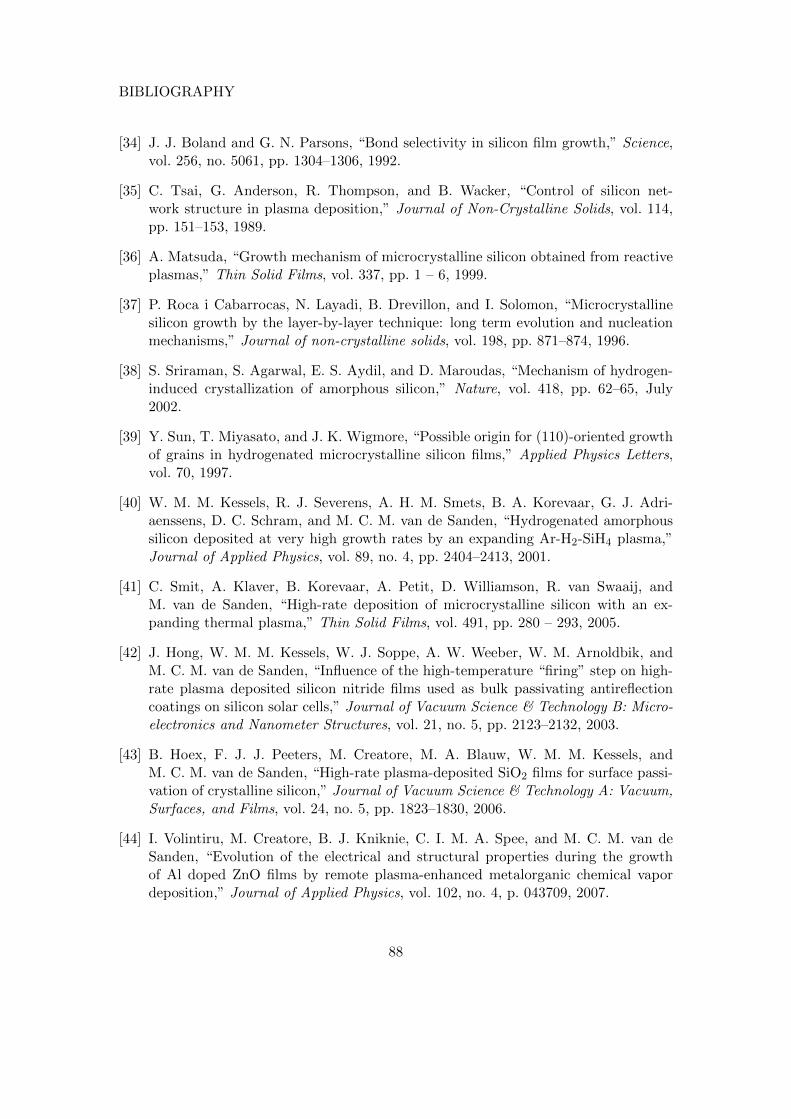
BIBLIOGRAPHY
[34] J. J. Boland and G. N. Parsons, “Bond selectivity in silicon film growth,” Science,vol. 256, no. 5061, pp. 1304–1306, 1992.
[35] C. Tsai, G. Anderson, R. Thompson, and B. Wacker, “Control of silicon net-work structure in plasma deposition,” Journal of Non-Crystalline Solids, vol. 114,pp. 151–153, 1989.
[36] A. Matsuda, “Growth mechanism of microcrystalline silicon obtained from reactiveplasmas,” Thin Solid Films, vol. 337, pp. 1 – 6, 1999.
[37] P. Roca i Cabarrocas, N. Layadi, B. Drevillon, and I. Solomon, “Microcrystallinesilicon growth by the layer-by-layer technique: long term evolution and nucleationmechanisms,” Journal of non-crystalline solids, vol. 198, pp. 871–874, 1996.
[38] S. Sriraman, S. Agarwal, E. S. Aydil, and D. Maroudas, “Mechanism of hydrogen-induced crystallization of amorphous silicon,” Nature, vol. 418, pp. 62–65, July2002.
[39] Y. Sun, T. Miyasato, and J. K. Wigmore, “Possible origin for (110)-oriented growthof grains in hydrogenated microcrystalline silicon films,” Applied Physics Letters,vol. 70, 1997.
[40] W. M. M. Kessels, R. J. Severens, A. H. M. Smets, B. A. Korevaar, G. J. Adri-aenssens, D. C. Schram, and M. C. M. van de Sanden, “Hydrogenated amorphoussilicon deposited at very high growth rates by an expanding Ar-H2-SiH4 plasma,”Journal of Applied Physics, vol. 89, no. 4, pp. 2404–2413, 2001.
[41] C. Smit, A. Klaver, B. Korevaar, A. Petit, D. Williamson, R. van Swaaij, andM. van de Sanden, “High-rate deposition of microcrystalline silicon with an ex-panding thermal plasma,” Thin Solid Films, vol. 491, pp. 280 – 293, 2005.
[42] J. Hong, W. M. M. Kessels, W. J. Soppe, A. W. Weeber, W. M. Arnoldbik, andM. C. M. van de Sanden, “Influence of the high-temperature “firing” step on high-rate plasma deposited silicon nitride films used as bulk passivating antireflectioncoatings on silicon solar cells,” Journal of Vacuum Science & Technology B: Micro-electronics and Nanometer Structures, vol. 21, no. 5, pp. 2123–2132, 2003.
[43] B. Hoex, F. J. J. Peeters, M. Creatore, M. A. Blauw, W. M. M. Kessels, andM. C. M. van de Sanden, “High-rate plasma-deposited SiO2 films for surface passi-vation of crystalline silicon,” Journal of Vacuum Science & Technology A: Vacuum,Surfaces, and Films, vol. 24, no. 5, pp. 1823–1830, 2006.
[44] I. Volintiru, M. Creatore, B. J. Kniknie, C. I. M. A. Spee, and M. C. M. van deSanden, “Evolution of the electrical and structural properties during the growthof Al doped ZnO films by remote plasma-enhanced metalorganic chemical vapordeposition,” Journal of Applied Physics, vol. 102, no. 4, p. 043709, 2007.
88
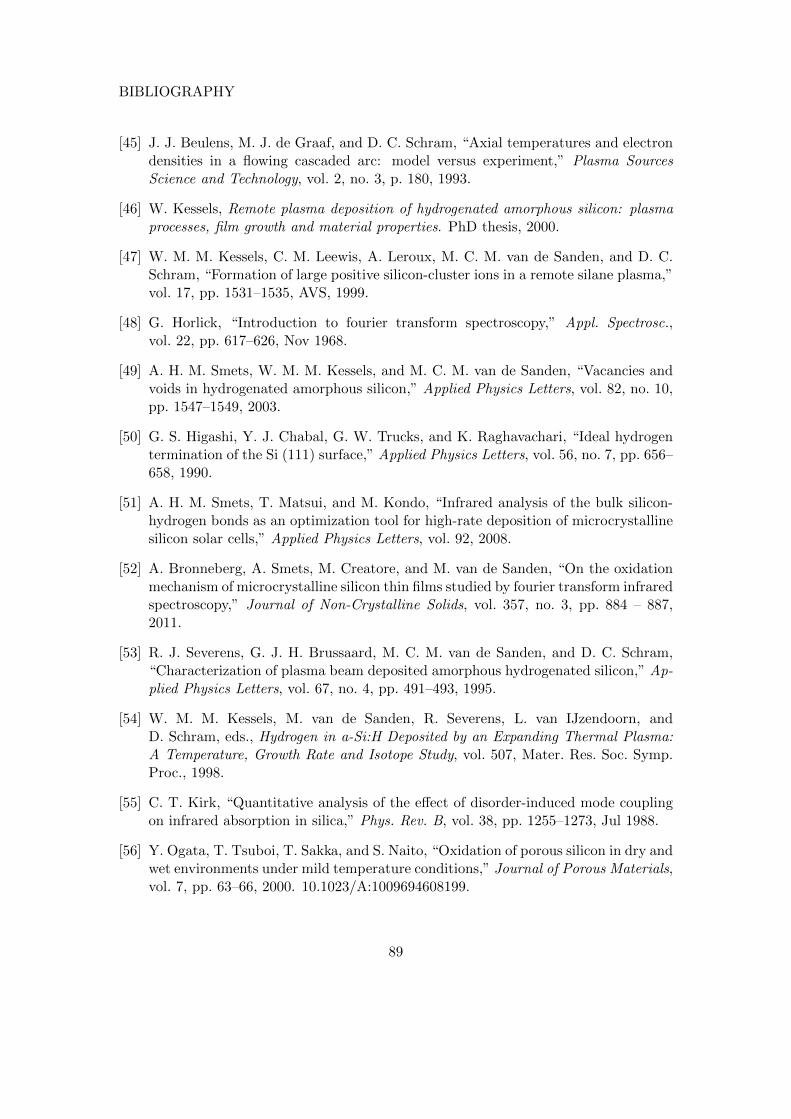
BIBLIOGRAPHY
[45] J. J. Beulens, M. J. de Graaf, and D. C. Schram, “Axial temperatures and electrondensities in a flowing cascaded arc: model versus experiment,” Plasma SourcesScience and Technology, vol. 2, no. 3, p. 180, 1993.
[46] W. Kessels, Remote plasma deposition of hydrogenated amorphous silicon: plasmaprocesses, film growth and material properties. PhD thesis, 2000.
[47] W. M. M. Kessels, C. M. Leewis, A. Leroux, M. C. M. van de Sanden, and D. C.Schram, “Formation of large positive silicon-cluster ions in a remote silane plasma,”vol. 17, pp. 1531–1535, AVS, 1999.
[48] G. Horlick, “Introduction to fourier transform spectroscopy,” Appl. Spectrosc.,vol. 22, pp. 617–626, Nov 1968.
[49] A. H. M. Smets, W. M. M. Kessels, and M. C. M. van de Sanden, “Vacancies andvoids in hydrogenated amorphous silicon,” Applied Physics Letters, vol. 82, no. 10,pp. 1547–1549, 2003.
[50] G. S. Higashi, Y. J. Chabal, G. W. Trucks, and K. Raghavachari, “Ideal hydrogentermination of the Si (111) surface,” Applied Physics Letters, vol. 56, no. 7, pp. 656–658, 1990.
[51] A. H. M. Smets, T. Matsui, and M. Kondo, “Infrared analysis of the bulk silicon-hydrogen bonds as an optimization tool for high-rate deposition of microcrystallinesilicon solar cells,” Applied Physics Letters, vol. 92, 2008.
[52] A. Bronneberg, A. Smets, M. Creatore, and M. van de Sanden, “On the oxidationmechanism of microcrystalline silicon thin films studied by fourier transform infraredspectroscopy,” Journal of Non-Crystalline Solids, vol. 357, no. 3, pp. 884 – 887,2011.
[53] R. J. Severens, G. J. H. Brussaard, M. C. M. van de Sanden, and D. C. Schram,“Characterization of plasma beam deposited amorphous hydrogenated silicon,” Ap-plied Physics Letters, vol. 67, no. 4, pp. 491–493, 1995.
[54] W. M. M. Kessels, M. van de Sanden, R. Severens, L. van IJzendoorn, andD. Schram, eds., Hydrogen in a-Si:H Deposited by an Expanding Thermal Plasma:A Temperature, Growth Rate and Isotope Study, vol. 507, Mater. Res. Soc. Symp.Proc., 1998.
[55] C. T. Kirk, “Quantitative analysis of the effect of disorder-induced mode couplingon infrared absorption in silica,” Phys. Rev. B, vol. 38, pp. 1255–1273, Jul 1988.
[56] Y. Ogata, T. Tsuboi, T. Sakka, and S. Naito, “Oxidation of porous silicon in dry andwet environments under mild temperature conditions,” Journal of Porous Materials,vol. 7, pp. 63–66, 2000. 10.1023/A:1009694608199.
89
BIBLIOGRAPHY
[57] C. V. Raman and K. S. Krishnan, “A new type of secondary radiation,” Nature,vol. 121, no. 3048, pp. 501–502, 1928.
[58] E. Smith and G. Dent, Modern Raman Spectroscopy: A Practical Approach. JohnWiley & Sons, 2005.
[59] C. Smit, R. A. C. M. M. van Swaaij, H. Donker, A. M. H. N. Petit, W. M. M.Kessels, and M. C. M. van de Sanden, “Determining the material structure ofmicrocrystalline silicon from Raman spectra,” Journal of Applied Physics, vol. 94,no. 5, pp. 3582–3588, 2003.
[60] A. T. Voutsas, M. K. Hatalis, J. Boyce, and A. Chiang, “Raman spectroscopy ofamorphous and microcrystalline silicon films deposited by low-pressure chemicalvapor deposition,” Journal of Applied Physics, vol. 78, no. 12, pp. 6999–7006, 1995.
[61] R. Tsu, J. Gonzalez-Hernandez, S. S. Chao, S. C. Lee, and K. Tanaka, “Criticalvolume fraction of crystallinity for conductivity percolation in phosphorus-dopedSi:F:H alloys,” Applied Physics Letters, vol. 40, no. 6, pp. 534–535, 1982.
[62] E. Bustarret, M. A. Hachicha, and M. Brunel, “Experimental determination of thenanocrystalline volume fraction in silicon thin films from Raman spectroscopy,”Applied Physics Letters, vol. 52, no. 20, pp. 1675–1677, 1988.
[63] H. Fujiwara, Spectroscopic ellipsometry: Principles and Applications. John Wiley& Sons, 2007.
[64] M. G. N. C. Suryanarayana, X-Ray diffraction: a practical approach. SpringerScience, 1998.
[65] J. I. Langford and A. J. C. Wilson, “Scherrer after sixty years: A survey and somenew results in the determination of crystallite size,” Journal of Applied Crystallog-raphy, vol. 11, pp. 102–113, Apr 1978.
[66] W. van Sark, J. Bezemer, and W. van der Weg, “Role of ions in PECVD of amor-phous silicon,” Surface and Coatings Technology, vol. 74, pp. 63–66, 1995.
[67] X.-Z. Bo, N. Yao, S. R. Shieh, T. S. Duffy, and J. C. Sturm, “Large-grain poly-crystalline silicon films with low intragranular defect density by low-temperaturesolid-phase crystallization without underlying oxide,” Journal of Applied Physics,vol. 91, no. 5, pp. 2910–2915, 2002.
[68] W. M. M. Kessels, M. C. M. van de Sanden, and D. C. Schram, “Film growthprecursors in a remote SiH4 plasma used for high-rate deposition of hydrogenatedamorphous silicon,” Journal of Vacuum Science & Technology A: Vacuum, Surfaces,and Films, vol. 18, no. 5, pp. 2153–2163, 2000.
[69] W. Kessels, A. Smets, D. Marra, E. Aydil, D. Schram, and M. van de Sanden, “Onthe growth mechanism of a-Si:H,” Thin Solid Films, vol. 383, pp. 154 – 160, 2001.
90
BIBLIOGRAPHY
[70] P. K. Giri, S. Tripurasundari, G. Raghavan, B. K. Panigrahi, P. Magudapathy,K. G. M. Nair, and A. K. Tyagi, “Crystalline to amorphous transition and bandstructure evolution in ion-damaged silicon studied by spectroscopic ellipsometry,”Journal of Applied Physics, vol. 90, no. 2, pp. 659–669, 2001.
[71] H. Fujiwara, M. Kondo, and A. Matsuda, “Nucleation mechanism of microcrys-talline silicon from the amorphous phase,” Journal of non-crystalline solids, vol. 338,pp. 97–9101, 2004.
[72] H. Fujiwara, Y. Toyoshima, M. Kondo, and A. Matsuda, “Nucleation mechanism ofmicrocrystalline silicon studied by real time spectroscopic ellipsometry and infraredspectroscopy,” MRS Proceedings, vol. 609, no. 1, 2000.
[73] H. Fujiwara, M. Kondo, and A. Matsuda, “Real-time spectroscopic ellipsometrystudies of the nucleation and grain growth processes in microcrystalline silicon thinfilms,” Physical Review B, vol. 63, no. 11, 2001.
[74] M. A. Wank, R. A. C. M. M. van Swaaij, and M. C. M. van de Sanden, “On thesurface roughness development of hydrogenated amorphous silicon deposited at lowgrowth rates,” Applied Physics Letters, vol. 95, no. 2, p. 021503, 2009.
[75] H. Fujiwara, Y. Toyoshima, M. Kondo, and A. Matsuda, “Interface-layer formationmechanism in a − Si : H thin-film growth studied by real-time spectroscopic ellip-sometry and infrared spectroscopy,” Phys. Rev. B, vol. 60, pp. 13598–13604, Nov1999.
[76] K. Sharma, M. V. Ponomarev, M. A. Verheijen, O. Kunz, F. D. Tichelaar, M. C. M.van de Sanden, and M. Creatore, “Solid-phase crystallization of ultra high growthrate amorphous silicon films,” Journal of Applied Physics, vol. 111, no. 10, p. 103510,2012.
[77] W. M. M. Kessels, A. Leroux, M. G. H. Boogaarts, J. P. M. Hoefnagels, M. C. M.van de Sanden, and D. C. Schram, “Cavity ring down detection of SiH3 in a re-mote SiH4 plasma and comparison with model calculations and mass spectrometry,”Journal of Vacuum Science & Technology A: Vacuum, Surfaces, and Films, vol. 19,no. 2, pp. 467–476, 2001.
91