efficiency and throughput advances in continuous roll … · november 1999 • nrel/sr-520-27535...
TRANSCRIPT

November 1999 • NREL/SR-520-27535
M. IzuEnergy Conversion Devices, Inc.Troy, Michigan
Efficiency and ThroughputAdvances in ContinuousRoll-to-Roll a-Si Alloy PVManufacturing Technology
Annual Technical Progress Report22 June 1998 21 June 1999
National Renewable Energy Laboratory1617 Cole BoulevardGolden, Colorado 80401-3393NREL is a U.S. Department of Energy LaboratoryOperated by Midwest Research Institute •••• Battelle •••• Bechtel
Contract No. DE-AC36-98-GO10337

November 1999 • NREL/SR-520-27535
Efficiency and ThroughputAdvances in ContinuousRoll-to-Roll a-Si Alloy PVManufacturing Technology
Annual Technical Progress Report22 June 1998 21 June 1999
M. IzuEnergy Conversion Devices, Inc.Troy, Michigan
NREL Technical Monitor: R.L. MitchellPrepared under Subcontract No. ZAX-8-17647-09
National Renewable Energy Laboratory1617 Cole BoulevardGolden, Colorado 80401-3393NREL is a U.S. Department of Energy LaboratoryOperated by Midwest Research Institute •••• Battelle •••• Bechtel
Contract No. DE-AC36-98-GO10337

NOTICE
This report was prepared as an account of work sponsored by an agency of the United Statesgovernment. Neither the United States government nor any agency thereof, nor any of their employees,makes any warranty, express or implied, or assumes any legal liability or responsibility for the accuracy,completeness, or usefulness of any information, apparatus, product, or process disclosed, or representsthat its use would not infringe privately owned rights. Reference herein to any specific commercialproduct, process, or service by trade name, trademark, manufacturer, or otherwise does not necessarilyconstitute or imply its endorsement, recommendation, or favoring by the United States government or anyagency thereof. The views and opinions of authors expressed herein do not necessarily state or reflectthose of the United States government or any agency thereof.
Available electronically at http://www.doe.gov/bridge
Available for a processing fee to U.S. Department of Energyand its contractors, in paper, from:
U.S. Department of EnergyOffice of Scientific and Technical InformationP.O. Box 62Oak Ridge, TN 37831-0062phone: 865.576.8401fax: 865.576.5728email: [email protected]
Available for sale to the public, in paper, from:U.S. Department of CommerceNational Technical Information Service5285 Port Royal RoadSpringfield, VA 22161phone: 800.553.6847fax: 703.605.6900email: [email protected] ordering: http://www.ntis.gov/ordering.htm
Printed on paper containing at least 50% wastepaper, including 20% postconsumer waste

2
PREFACE
This Phase I annual technical progress report covers the work performed by Energy Conversion Devices, Inc.(ECD) for the period of June 22, 1998 through June 21, 1999 under DOE/NREL Subcontract No. ZAX-8-17647-09 entitled “Efficiency and Throughput Advances in Continuous Roll-to-Roll a-Si Alloy PV ManufacturingTechnology.” This is the first Annual Technical Progress Report for this subcontract. The subcontract isscheduled to be performed from June 22, 1998 through June 21, 2001. The following personnel at ECD haveparticipated in this program:
Hank BianchiGennady BondarenkoRay CrucetJoe DoehlerTim EllisonEric HaggardMasat IzuScott JonesRob KopfArun KumarArt MyattHerb Ovshinsky
This program has been supported by the following United Solar personnel:
Eric AkkashianArindam BanerjeeJon CallSubhendu GuhaKevin HoffmanMark LycetteGerard PietkaMike WaltersJeff Yang
This program has also been supported by our subcontractor Scientific Applications International Corp. (SAIC).SAIC staff that worked on this program include:
Ellis HymanBarton Lane

3
EXECUTIVE SUMMARY
The objective of this program over the three-year period is to continue to advance ECD’s amorphous silicon (a-Si)solar cell PV manufacturing technology to improve the stable module efficiency to increase the throughput, toreduce the manufacturing costs, and to pave the way for production expansion. The three-year goal is to achieve a25-30% reduction in module cost ($/W) and a 60% increase in manufacturing capacity (MW/Year) over theUnited Solar’s 1997 4th Quarter annual manufacturing capacity.
To achieve this objective, ECD shall perform the following tasks:
1. Development, design and installation of improved heating system for United Solar’s continuous roll-to-roll a-Si deposition machine,
2. Development of new in-line hardware and software cell diagnostic systems that can be used for in-lineQA/QC and on-line continuous process optimization,
3. Advance the new backreflector deposition process in order to reduce the cost and to obtain higher depositionrates,
4. Development of a new cathode hardware design which will demonstrate and improve solar cell performanceand deposition uniformity.
During the first-year Phase I program, ECD proposed to perform the following four tasks:
Task 1: Process Control Improvements: Substrate Heating and Temperature Monitoring SystemsTask 2: Process Control Improvements: In-Line Characterization SensorsTask 3: Improvements to Backreflector Deposition ProcessTask 4: Improvements in the a-Si Deposition Cathode Configuration
Major Accomplishments in this Phase I Program:
1. Completed design and construction of new, improved substrate heater.2. Tested and verified improved performance of the new substrate heater in the pilot machine.3. Verified improved performance of the new substrate heater in the production machine.4. Designed and bench-tested a new infrared temperature sensor.5. Installed a prototype new infrared temperature sensor in the production machine for evaluation.6. Designed a new rolling thermocouple temperature sensor.7. Designed and bench-tested a reflectometer for the backreflector deposition machine.8. Designed and bench-tested in-line non-contacting cell diagnostic sensor; PV capacitive diagnostic (PVCD)
system.9. Installed the in-line cell diagnostic sensor in the 5 MW a-Si deposition machine for evaluation.10. Demonstrated a new low-cost zinc metal process in the pilot backreflector machine.11. Fully tested a new cathode design for improved uniformity.

4
TABLE OF CONTENTSPage
Preface 2Executive Summary 3Table of Contents 4List of Figures 6List of Tables 8Background 9 Overview of ECD/United Solar’s PV Manufacturing Technology 9 Current Manufacturing Procedures 10 Advantages of the Present Manufacturing Process 12 Problems with the Present Manufacturing Process 12Task 1 - Process Control Improvements: New Substrate Heating and Temperature Monitoring Systems 14 The New Substrate Heating System 14 Introduction 14 System Design 14 Work Performed 15 Summary Evaluation: Improved Substrate Heaters 17 New Temperature Monitoring Systems 19 Introduction 19 IR Temperature Sensor 19 Description of IR Temperature Sensors 21 Rolling Thermocouple Concept 23 Testing the New Temperature Monitoring Systems 23Task 2 - Process Control Improvements: Development of In-Line Sensors and Diagnostic Systems 25 Introduction 25 Backreflector Characterization Sensors 26 Objectives 26 Benchtop System Descriptions 26 Backreflector ZnO Film Thickness Measurement System 26 Backreflector Scatterometer 26 Data Analysis: Backreflector Scatterometer 28 Laser Diode Stability 28 Sample Measurements 28 Light I-V Correlation Studies 30 Correlation vs. Scattering Angle 30 Dependence of Diffuse Reflectance on Incident Angle 32 Data Analysis: ZnO Thickness Measurement 33 2nd Generation Sensor Development 33 Backreflector Scatterometer 33 Backreflector ZnO Film Thickness Measurement System 33 PV Capacitive Diagnostic (PVCD) System 34 Introduction 34 Principle Of Operation 34

5
TABLE OF CONTENTS (continued)
Page
Bench-Top System Design 35 Establish Basic Operation 36 Compensation for Finite Time Constant 37 Measurement Reproducibility 38 Summary of Selected Preliminary Measurements 38 Design of the Second Generation Device for Installation in the 5 MW 40Task 3 – Development of Reactive Sputtering Process Using Inexpensive Zn Metal Targets for Back Reflector Preparation 42 Background 42 Objective of Backreflector Studies 43 Experimental 43 Results of Work Completed During Phase I of the Program 44 Web Handling Procedures 44 Reactive Sputtering Optimization 46 Preparation for Tests in 5MW Production Machine 48 Plans for Phase II of the Program 49Task 4 - Cathode Hardware Studies for a-Si(Ge):H i-layer Depositions 50 Background 50 Objective of Cathode Hardware Studies 51 Experimental 52 Results of Work Completed During Phase I of the Program 54 The 5MW Style Cathode in the Single R&D Chamber 54 Testing Similarity to Cathodes Used in Production 54 Attempts to Improve Uniformity Using 5 MW Style Cathode 56 Testing of New Cathode Design in the Single R&D Chamber 57 Establishment of Baseline “5MW-like” Cathode in Pilot Roll-to-Roll Machine 60 Plans for Phase II of the Program 60 Modeling for Amorphous Silicon Deposition 61 Introduction 61 Simulation Strategy 61 One-Point Simulations 62 RF-Global Simulation 62 The Boltzmann Code 63

6
LIST OF FIGURES Page
Figure A. Structure of a triple-junction spectrum-splitting solar cell producedin the ECD/United Solar continuous roll-to-roll manufacturing process. 9
Figure B. Schematic drawing of ECD’s roll-to-roll solar cell deposition process. 10Figure 1 Photograph of a quartz IR heating lamp from the 5 MW production machine. 14Figure 2 Photograph of the new low temperature ribbon heater element. 15Figure 3 Mechanical schematic of the experimental housing for the ribbon heaters. 16Figure 4 Temperature profile at the two extreme shapes possible with the housing
shown in the previous figure. 16Figure 5 Ribbon-type heaters installed in the production machine. 18Figure 6 Ribbon heater assembly detail. 18Figure 7 Polar radiation pattern from heated surfaces. 19Figure 8 Infrared sensor installed on production machine. 21Figure 9 Copy of blueprint showing installed temperature sensor. 22Figure10 Layout of the new cathode test system being designed for installation in the
pilot amorphous Si machine showing the two new rolling thermocouple assemblies. 24Figure 11 Schematic of the benchtop backreflector ZnO film thickness measurement system. 27Figure 12 Schematic of the benchtop backreflector scatterometer. 27Figure 13 Diffuse reflection comparison of various samples. 29Figure 14 Plot of correlation coefficients for each cell parameter calculated at single scattering
angles (17 R&D samples). 31Figure 15 Plot of correlation coefficients for each cell parameter calculated at single scattering
angles (12 5BR production samples). 31Figure 16 Schematic of the modified scatterometer configuration. 32Figure 17 Comparison of light scatter for 5BR 531 using 2 different angles of incidence.
“Angle” is with respect to the specularly reflected beam. 32Figure 18 Electrical schematic of the PVCD. 34Figure 19 Light (laser) and voltage waveforms from the PVCD. 35Figure 20 Photograph of the PVCD bench-test system. The oscilloscope is displaying
the waveforms of the laser pulse (the step function) and the output of the PVCD.Notice the similarity between the stored traces on the oscilloscope and thewaveforms in Figure 18. 36
Figure 21 Oscilloscope traces of a PV cell using both the bench-top PVCD (upper trace) anda probe in direct contact with the ITO. (10 ms/div). The laser is pulsed on after
10 ms, and switched of after 20 ms. 37Figure 22 Measurement of PVCD time constant. A simple single pole filter with a time constant of 1.3686, fits the data over 3 seconds with less than a 0.01% relative error. 37Figure 23 Oscilloscope traces of the laser diode module current monitor (top) and output of a photodetector (bottom). The oscilloscope recorded the peak voltages for each of these signals. 38Figure 24 PVCD waveforms and fitted curves resulting from a 4-parameter fit. 39Figure 25 Parameter resulting from fit of PVCD waveform plotted vs. measured open
circuit voltage for cell with a different number of layers. 39Figure 26 Mechanical schematic showing the mounting of the PVCD in the take-up chamber of the 5 MW. 41Figure 27 United Solar’s roll-to-roll backreflector machine. This machine is also part of
United Solar’s decommissioned 2 MW plant and will be used for the bulk ofTask 2, and for part of Task 1. 44

7
List of Figures (continued) Page
Figure 28 Dependence of Jsc for a-SiGe:H cells on oxygen flow. 46Figure 29 Variation of Ge content and deposition rate across cathode. 51Figure 30 Double-junction roll-to-roll plasma-CVD processor, previously used as
United Solar’s production machine. This machine will be used as an experimental machine for much of the work proposed in Tasks 1 and 3. 52
Figure 31 Single chamber system used for cathode development. 53Figure 32 a-Si:H single-junction cell structure. 53Figure 33 Thickness profiles for films made at different applied rf powers. 55Figure 34 Orientation of film thickness measurements. 55Figure 35 Variation of deposition uniformity over length of cathode as a function
of deposition rate. 56Figure 36 Uniformity across width of web (cathode) from deposits made using
different gas flows from outside cathode and gas manifold hardware. 57Figure 37 Deposition rate profiles across new cathode at different deposition rates. 58Figure 38 Plot of fill factor versus short circuit current for cells made using the
new and 5MW style cathodes. 59Figure 39 Plot of efficiency versus short circuit current for cells made using the new
and 5MW style cathodes. 59Figure 40 Electron Impact Cross Sections (cm2):(a-f) a. H2 momentum transfer; 66
b. Lowest threshold H optical excitation; 67c. SiH4 optical excitation; 68d. H2 ionization; 69e. lowest threshold H2 vibrational excitation; 70f. lowest threshold SiH4 vibrational excitation; 71g. dissociative attachment from the v=1 and v=2 vibrational states of H2. 72
Figure 41 Modeled RF Reactor Subchamber Design. 73Figure 42 Electron Energy Distribution Functions at Various Times after Turn-on:(a-d) a. 1.75x10⁻⁸ s; 75
b. 1.34x10⁻⁶ s; 76c. 9.77x10⁻⁵ s; 77d. 9.90x10⁻³ s. 78
Figure 43 Evolution of Neutral Species (cm-3):(a-e) a. H2, SiH4, H, SiH3, Si2H6: 79
b. H2, H2(v=1), H2(v=2); 80c. Si2H5, SiH2, SiH, Si; 81d. Si2H4, Si2H2, Si2H, Si2; 82e. Si2H3, Si3H8, Si3H5, Si3H4. 83
Figure 44 Evolution of Positive Ions (cm-3): (a-c) a. SiH3
+, SiH2+, SiH+, Si2H7
+, Si2H5+; 84
b. Si2H4+, Si2H3
+, Si2H2+, Si2H+, Si3H7
+; 85c. Si3H6
+, Si3H5+, Si3H4
+, H3+, H2
+, H+. 86Figure 45 Evolution of Negative Ions (cm-3) : H-, SiH3
-, Si2H5-, Si3H7
-. 87Figure 46 Evolution of Positive and Negative Ions and Electrons (cm-3): total
positive ions, total negative ions, electrons. 89Figure 47 Evolution of Average Electron Energy (ev). 90Figure 48 Measured Thickness of Amorphous Silicon Deposition (nm) in Reactor. 91

8
List of Tables
Page
Table 1 Ribbon Heater Engineering Details. 17Table 2 Influence of Various Stray Objects. 20Table 3 Correlation Coefficients for 5BR# 534 Samples. 30Table 4 Measured Reflection Minima for 15 R&D Backreflector Samples. 33Table 5 Comparison of Data for a-Si:H Cells Co-Deposited on Al/ZnO
Backreflectors. Cell Measurements Completed Using AM1.5 Light. 42Table 6 Data for Cells Prepared Using the Different Backreflectors after
Different Exposure Environments and Exposure Times. 45Table 7 Data for a-SiGe:H Cells Prepared with Backreflectors Made Using
Reactive Sputtering Technique Under a Variety of Deposition Conditions. 47Table 8 Data for a-SiGe:H Cells Whose Backreflectors were Made Using Targets
With Different Al Contents. 47Table 9 Data for a-SiGe:H Cells Whose Backreflectors were Made with the Reactive
Sputtering Process Using Zn Metal Targets and the Standard Process UsingZnO Targets. 48
Table 10 Data for 44.5 cm2 Modules Made With Different Backreflectors. 48Table 11 Data for a-SiGe:H Cells Made at Different Applied Powers but Similar i-layer
Deposition Rates. 56Table 12 Data for a-SiGe:H Cells Made Using the New and the 5 MW Style Cathodes. 59

9
BACKGROUND
Overview of ECD/United Solar’s PV Manufacturing Technology
Key features of ECD/United Solar’s photovoltaic manufacturing technology are summarized below.
Spectrum Splitting, Triple-Junction Cell DesignHigh conversion efficiencies are obtained by using a triple-junction triple-bandgap cell that has high-qualitybandgap profiled a-SiGe alloy for the middle and bottom intrinsic layers. The cell structure is shown in Figure A.
S t a i n l e s s S t e e l S u b s t r a t e
T e x t u r e d B a c k R e f l e c t o r A g / Z n On - t y p e a - S i : H a l l o y
i - t y p e a - S i G e : H a l l o y
n - t y p e a - S i : H a l l o yp - t y p e m i c r o c r y s t a l l i n e S i a l l o y
i - t y p e a - S i G e : H a l l o y
p - t y p e m i c r o c r y s t a l l i n e S i a l l o yn - t y p e a - S i : H a l l o y
i - t y p e a - S i : H a l l o yp - t y p e m i c r o c r y s t a l l i n e S i a l l o y
T r a n s p a r e n t C o n d u c t i v e O x i d eG r i d P a t t e r n
Figure A. Structure of a triple-junction spectrum-splitting solar cell produced in the ECD/United Solar continuous roll-to-roll manufacturing process.
United Solar has recently demonstrated 14.6% initial and 13% stable, small-area energy conversion efficiency a-Si alloy solar cell devices with an a-Si//a-SiGe//a-SiGe triple-junction design. United Solar has also demonstratedstable 10.2% efficiency for a 1 ft2 panel using this triple junction solar cell design.
Low-cost, large-scale continuous roll-to-roll operationThe nine layers of a-Si alloy material used in the solar cell are deposited sequentially in a single pass onto a 2500ft. long substrate in a roll-to-roll process, as is shown in Figure B. This stable steady-state process has proven tobe reliable and capable of producing cells with a high degree of uniformity. The operating cost, which includesmaterials, maintenance and labor, is low.
Flexible thin stainless steel substrateThe substrate, a 5 mil thick, 14 in. wide, 2500 ft long stainless steel roll has many advantages over glasssubstrates: (1) it is lightweight, flexible, and will not shatter or be damaged during manufacture, handling, andsubsequent operation in the field; (2) the thin stainless steel substrate has a thermal time constant of less than 10ms and, consequently, can be quickly heated and cooled, thus eliminating any waiting time for temperaturestabilization; and (3) the substrate transport mechanism in the deposition chambers is simple and reliable withnegligible component wear, resulting in very low machine maintenance costs.
Lightweight polymer encapsulated PV moduleEVA and Tefzel are used for module encapsulation. These modules are flexible, lightweight, and shatterproof.

10
G rid
S ta in less S tee l
A g /Z nON 1I1
N 2P 1
I2P 2N 3I3
P 3T C O
R o ll-to -R o ll M ach in e
N 1 I1 P 1 N 2 I2 P 2 N 3 I3 P 3
M o v in gS ta in le ss
S teelW eb
Figure B. Schematic drawing of ECD’s roll-to-roll solar cell deposition process.
Current Manufacturing Procedures
The present manufacturing plant in Troy, Michigan at United Solar, ECD’s manufacturing joint venture withCanon Inc., produces amorphous silicon alloy based solar cells and photovoltaic modules with a triple-junction,triple-bandgap configuration. ECD/United Solar’s proprietary roll-to-roll continuous substrate process isemployed to produce complete solar cell structures on stainless steel rolls. These rolls, typically 2500 ft. long, 14in. wide, and 5 mil thick, are processed at 2 ft. per minute.
The stainless steel rolls are coated consecutively, in roll-to-roll deposition machines, with a back reflectorconsisting of a metal and metal oxide layer, nine layers of amorphous silicon alloy, and a transparent conductingoxide top contact layer. The rolls are then cut into appropriate sizes for assembly into photovoltaic modules.
ECD/United Solar’s proprietary solar cell manufacturing process is divided into two distinct sequences: (1) roll-to-roll solar cell deposition (front-end), and (2) module assembly (back-end). The ability to divide manufacturinginto these two sequences which can be located in quite different locations, is a unique advantage of our process.The output of the front end feeds the semi-automated back-end assembly lines in place for producing 17 differentproducts: 7 types of framed rigid modules; 3 types of flexible modules; 2 types of folding modules and 5 types ofbuilding integrated roofing modules.
Specifically, our current solar cell production involves the following process steps and equipment:
I. Current Front-End Roll-to-Roll Deposition Plant for Solar Cell Production
I.1 Substrate Washing MachineThe stainless steel roll, purchased from a supplier, is first washed to produce clean, dry, particle-free substratematerial suitable for a-Si alloy deposition. The washing machine is a continuous roll-to-roll processing systemwhich transports the stainless steel web though a detergent cleaning station, multiple de-ionized water rinsingbaths, and an infrared drying oven.

11
I.2 Back-Reflector MachineThe roll is then transferred to the back-reflector (BR) machine, also a continuous roll-to-roll processing system.The BR machine sequentially deposits a reflective metal alloy layer and a metal oxide “buffer” layer onto thecleaned stainless steel web by magnetron sputtering. The proprietary metal alloy and metal oxide buffer layersprovide ohmic contact to the solar cell and an improved infrared response. The metal alloy layer adheres to thestainless steel and texturizes the surface to provide a diffuse optically-reflective layer. This texturing enhancesabsorption of the infrared portion of the solar spectrum by providing an increased optical length for reflected lightin the thin film solar cell structure.
I.3 Amorphous Silicon Alloy Deposition MachineAfter the back-reflector deposition, the roll is loaded into the amorphous silicon alloy deposition machine. Thismachine is a continuous roll-to-roll rf plasma-enhanced CVD processing system which sequentially deposits, in asingle pass, nine thin films of doped and undoped amorphous silicon alloy semiconductors.
Mixtures of feedstock gases are decomposed at a pressure of approximately 1 Torr in a series of rf PECVDplasma chambers to continuously deposit amorphous thin film layers onto the substrate which is heated toapproximately 250°C. The multi-section amorphous silicon alloy deposition machine consists of a pay-offchamber section, nine process chamber sections for deposition of the triple (graded) junction, triple bandgap solarcells, and a take-up section. The process gas mixture in each deposition chamber is dynamically isolated fromadjacent chambers by proprietary “gas gates” that isolate the gas mixtures in adjacent chambers even though noactual physical impediment is present.
The substrate transport system, which controls the web speed, tension, and steering accurately positions thesubstrate in the various process chambers and ensures that the substrate is properly wound. The deposition takesplace on the underside of the substrate, thus minimizing film defects due to particulates.
I.4 Transparent Conducting Oxide (TCO) Deposition Machine
The substrate roll, now coated with back reflector and semiconductor layers, is finally transferred to anothercontinuous roll-to-roll machine which deposits a transparent electrically-conducting oxide (TCO) layer on top ofthe solar cell structure. The substrate is heated to approximately 200°C and the film is deposited by reactivesputtering of an indium-tin alloy in an oxygen atmosphere. The TCO layer has two functions: first, it provides anelectrical top contact between the current-generating photovoltaic layers and the current collection grid; second,its thickness is chosen so that it acts as an anti-reflective coating for the amorphous silicon alloy, thus increasingthe utilization of incident light.
II Current Semi-Automated Back-End Module Assembly Plant
II.I SlabbingA finished roll of TCO coated a-Si alloy solar cell material is cut by a semi-automatic press into 35.2 cm x 35.6cm “slabs”. The press also punches various geometric shapes at the edges of the slabs to facilitate laterinterconnect attachments.
II.2 QA/QCThe die press also cuts 10.2 cm x 35.6 cm samples at preset intervals throughout the deposition roll. Thesesamples are processed into test solar cells for QC qualification. In this manner, the entire deposited roll of solarcell material is characterized.II.3 TCO ScribingThe slabs are then processed through an automated machine that etches the ITO from the borders of the cells; thecell size is electronically selectable.

12
II.4 Short PassivationDefects in the solar cell that could give rise to electrical shorts on the coated web are electrically isolated byelectrolytically converting the transparent top conductor into an insulator at the defect sites through a proprietaryprocess. This automatic short passivation operation involves treating the web with electrolyte solution andsubjecting the cell to reverse electrical bias. After short passivation, the residual electrolyte is rinsed off with de-ionized water, and the web is dried with hot air. This process is also performed by an automated machine.
II.5 Screen Print Grid PatternAnother automated machine is used to apply the collection grid wires to the cells, and then coat the cells with aclear lacquer.
II.6 Final AssemblyThe final assembly process includes the following steps:• Cell Interconnect - Cells are interconnected to make the cell block assembly. Suitable fixtures are provided to
ease the assembly process.• Laminating - The finished cell block is laminated in a vacuum laminator. Tefzel and EVA are used for the
front cover.• Module Finishing - The laminated cell block is trimmed to size and a junction box is attached. Other framing
and connector details are added for specific products.• Testing and Packaging - The module is finally tested in a solar simulator which measures the I-V curve of the
finished modules under simulated AM 1.5 conditions and provides a printout of the I-V characteristics.Modules are then packaged, ready for shipment.
Advantages of the Present Manufacturing Process
The ECD/United Solar a-Si alloy based thin film PV cell design and manufacturing technology offers severalfundamental advantages:1. Low semiconductor material cost; the device thickness is < 1 µm,2. Low-process cost; the continuous roll-to-roll process offers significant economies of scale as the process is
scaled up,3. Thin stainless steel substrate; the ECD/United Solar PV modules are lightweight, rugged, and flexible. This
reduces the installed cost of PV systems. In addition, there is a significant cost advantage in handling andprocessing the flexible stainless steel substrate, as compared with other substrates,
4. The modules are composed entirely of environmentally safe materials.
Problems with the Present Manufacturing Process
During the start-up and optimization of the new United Solar 5 MW plant, which was designed and constructedby ECD, a number of manufacturing processing and hardware problems that limit stable module efficiency, yield,and throughput have been identified. With the expanded back-end facilities, including the addition of automatedprocessing equipment, improvements in the throughput of the new front-end equipment will provide substantialeconomy of scale module cost reductions. In addition the stable efficiency of the PV modules, which arecurrently being manufactured at United Solar, is approximately 30% lower than that which can be expected fromdata obtained in the batch processes. The purpose of this program is to solve and implement solutions for the keyproblems that are limiting the module throughput of the 5 MW plant and the conversion efficiency of themodules. Below we review the major factors that are limiting the throughput of the equipment and the stableconversion efficiency of the modules.

13
1. Breakage of the quartz IR lamps that are used in the deposition machines to heat the substrate leads toconsiderable downtime, and expense. The IR lamp’s quartz envelope becomes coated over time by straydepositing species diffusing out of the reaction zones. This coating absorbs the lamp’s IR radiation andthermally stresses the glass envelope, which cracks after time.
2. The process consistency of the machine can be further improved. Typically, the efficiency of solar cells
produced on a 2500 ft. long stainless steel roll substrate varies by as much as 10% within one roll. Thisproblem, and uncontrolled run-to-run variations in material quality, also make it extremely difficult toadiabatically fine tune to processes to maximize the cell efficiency. Furthermore, data from QA/QCanalysis is available until after final deposition of the TCO onto the roll of solar cells and the roll isslabbed. This delay in feedback limits the effectiveness of ongoing optimization and may result in largeyield losses when a machine malfunctions. These shortcomings can be traced to the lack of on-linesensing devices which can monitor the quality of the material produced in the machines and correlatethese data with other processing variables and the results of QA/QC measurements.
3. The performance of the back-reflector material produced in the 5 MW line at production line speed results
in PV cell efficiency that is approximately 10% lower than that which can be obtained with thicker back-reflector produced at slower line speeds. We have made engineering compromises to sacrifice materialquality in order to maintain the required line speed. The present processing speed is limited by thesputtering of zinc-oxide; this processing step is also dominates the front-end material costs of the PVmaterial.
4. Another reason for lower stable efficiency results from the fact that the materials produced in large-scale
machines, including this 5 MW manufacturing line have significantly lower quality than the intrinsicmaterials produced in small-scale R&D machines.

14
Task 1 - Process Control Improvements:New Substrate Heating and Temperature Monitoring Systems
The New Substrate Heating System
Introduction
A new heating system has been designed and tested. The lifetime of the heater elements used in this new systemis at least an order of magnitude higher than the lifetime of the heaters used in the previous system. This newsystem will eliminate the cost of replacement heaters, unscheduled downtime due to heater breakage, andscheduled downtime for replacing heaters.
The new substrate heating system was of high priority due to the unreliability of the present quartz IR heatersinstalled when the new 5 MW production machine was built. The quartz IR heaters needed replacement at aboutan 8 – 10 week interval. The hardware cost alone for this replacement is on the order of 10 k$ per set. Also, therewere substantial additional costs associated with the downtime needed to change the lamps and lamp breakageleading to unscheduled downtime towards the end of the lamp lifetime. Consequently it was decided to acceleratethis program as much as possible. A prototype heater, using the new lower temperature metal ribbon heaters wasassembled and installed initially in the pilot machine and then in the production machine where we couldimmediately obtain reliability data in a production environment. The heater was installed in the I-1 chamberwhere the quartz IR heaters had the shortest lifetime. The system was monitored to determine if this new designwould be more reliable than the quartz IR heaters, and to determine what design changes would be needed toincrease their reliability.
System Design
Quartz IR lamp heaters have been used in our production machine to maintain the substrate temperature. Asshown in Figure 1, these lamps, because they run hot, accumulate thermally decomposed material on the envelopeof the lamp.
Figure 1. Photograph of a quartz IR heating lamp from the 5 MW production machine.

15
The accumulation of material, in combination with the unavoidable temperature cycles, eventually results insevere flaking and in physical stresses large enough to break the quartz envelopes. Even though the depositiontakes place on the underside of the substrate, the growing film is not protected from physical damage from theflakes and from the glass debris. Breakage of the quartz IR lamps that are used in the deposition machines to heatthe substrate further leads to considerable downtime, and expense.
We proposed to replace the quartz heaters in the roll-to-roll deposition machine with low-temperature, long-lasting NiChrome (a Nickel Chrome alloy) resistance heaters. These heaters operate at lower, more stable,temperatures. More importantly, they were thought to require little, if any, maintenance. They further offerconsiderable freedom in their design. We proposed to design, prototype, test, and retrofit the deposition machineswith a new substrate heating system using flat ribbon-shaped elements held in place over the web with ceramicinsulators, in a basic “flat sheet” configuration shown in Figure 2.
Figure 2. Photograph of the new low temperature ribbon heater element.
Work Performed
Ribbon heaters were initially installed in the pilot machine, using a housing that allowed the shape of the “flatsheet” to be adjusted to a large degree (see Figure 3).

16
Figure 3. Mechanical schematic of the experimental housing for the ribbon heaters.
The idea behind the adjustment is to be able to compensate for the generally higher temperatures the centerline ofthe web experiences with uniform heating. However, the temperature profile was found to be very insensitive tochanges in the shape of the heating surface (see Figure 4) and very similar in nature to the profile obtained withthe infrared lamps.
Figure 4. Temperature profile at the two extreme shapes possible with the housing shown in the previous figure.
Web Temperature Profile
305
310
315
320
325
330
335
340
345
0 2 4 6 8 10 12
Position across Web (in.)
Tem
pera
ture
(C)
Flat Prof ile
Arc

17
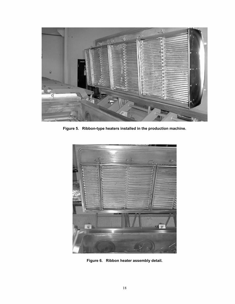
It soon became evident that the reliability of the ribbon heaters was vastly superior to that of the infrared lamps.So we decided, well ahead of schedule, to construct and install ribbon-type heaters in a portion of the productionmachine. The engineering details are listed in Table 1, while Figures 5 and 6 show their installation.
As of June 25, 1999, the ribbon heaters have been tested in many production runs without any failure nor any signof degradation. In contrast, the old style infrared lamps would have had to be replaced at least two times for asimilar production quantity, at a total material cost of at least $20,000.
Summary Evaluation: Improved Substrate Heaters
The improved substrate heaters have been installed in a portion of the roll-to-roll amorphous silicon productionmachine. They have operated without failure for over 100 production runs, without requiring maintenance otherthan visual inspection. The cost savings we anticipated in our proposal have been achieved well ahead ofschedule. We are currently working on improving the temperature uniformity across the web.
Table 1. Ribbon Heater Engineering Details.
Electrical Design Mechanical Design
Description Value Unit Description Value UnitWidth 0.375 Inches Elements per phase 2
Thickness 0.0285 Inches Rows per element 2Primary Voltage 480 V Spacing 0.125 inDesign Voltage 80 V Pitch 0.5 in
Connection Type Single Number of Strands 72Voltage per phase 80 V Loops / element 18
Power per phase 2.128 kW Wire per strand 10 inCurrent 26.6 A Straight Length 9.75 in
Cold Resistance 2.8643 Ohm Overall Loop Height 9.75 inMaterial "A" Wire per element 60.02 ft
Resistivity 510 Ohm/sq.mil
Loop Centers 1 in
Unit Resistance 0.04772 Ohm/ft O.A. length cc loops 17 inWire Core Temp. 900 F (Max) O.A. Length 17 7/8 in
Resistivity Change 1.05 xPower Density 3.66 W/sq.in
Length 60.02 ft/phaseUnit Weight 0.039 lb/ft
Length/lb 25.66 ft/lbTotal Weight /EL. 2.34 lb/ft
Elements/phase 1Phases 1
Total Power 2.13 kW/circuit
Total Ribbon 60.02 ftTotal Weight /EL. 2.34 lb
18
Figure 5. Ribbon-type heaters installed in the production machine.
Figure 6. Ribbon heater assembly detail.

19
New Temperature Monitoring Systems
Introduction
Accurate temperature sensing is essential in all of the deposition machines. The present sensor system used in ourproduction machines are thermocouples which are placed in close proximity of the back side of the substrate. Theaccuracy of the temperature measurement is based upon conductive heat transfer from the web to thethermocouple. As a result, while the temperature sensor system in the amorphous silicon machine is accurate dueto higher conductive heat transfer in the machine, the present sensors in the backreflector (BR) and top conductiveoxide (TCO) sputtering machines are not. The combination of an order of magnitude less conductive gas(Ar vs. H) and three orders of magnitude lower pressure, all but eliminate the thermal coupling between the weband the thermocouples in the BR and TCO machines. To solve this problem we are testing two new temperaturemonitoring systems: an IR temperature sensor system, and a rolling thermocouple design.
IR Temperature Sensor
The remote temperature sensor, based on the analysis of the blackbody radiation emitted by the heated stainlesssteel web, must have the following features:
• It should operate in a wavelength range at which the glass windows used on the vacuum vessels at theproduction machines are transparent. This constrains the wavelength range to less than 1.8um, approximately.
• Because the radiation emitted at those wavelengths, at the typical temperatures of interest, is small, efficientradiation detectors, operating near the room-temperature thermal detection limit are required. This constrainsthe detector types to Silicon-based semiconductor detectors, or to S1-type phototubes, both of which furtherlimit the possible wavelength range to near 1um.
• The sensor must further be capable of detecting the radiation from a specular surface, which reduces thealready-low emissivity of stainless steel.
• Objects with specular surfaces radiate blackbody energy at angles that differ from that emitted by diffuseobjects; the detector must therefore be configured to detect from specific angles. Figure 7 compares theblackbody emission from a diffuse surface ("A", on the left) with that of a specular one ("B", on the right):
Figure 7. Polar radiation pattern from heated surfaces.
As a result, the infrared blackbody radiation from a heated stainless steel web has initially been found to be ratherweak and difficult to detect. The infrared sensor we used is built around a Model M77LS infrared detector,manufactured by Mikron Instruments Company. Although adequate for the detection of the blackbody radiationfrom ordinary objects at elevated temperatures, it did not have, as received, sufficient sensitivity to detect the

20
signal from specular objects such as polished stainless steel, which forms the substrate onto which the solar cellswe produce are deposited. Only after positioning to detect radiation from a grazing angle was a signal detected.
Bench top measurements revealed:
• When comparing the temperature deduced from the infrared emission of polished stainless steel with thatfrom a piece of black, diffuse, graphite, both heated to 200C, differences in excess of 50C were observed.
• The temperature deduced from the infrared emission depends strongly on observation angle. Variations inobservation angles of +/-5 degrees introduce errors of the order of +/-40 C.
• Because the reflectivity of any specular surface unavoidably approaches 100% as the observation angle nearsgrazing incidence, the reflected images of stray objects come into any infrared sensor's field of view. If thetemperature of that stray object varies, its parasitic radiation affects the deduced temperature of the section ofweb of interest. Table 2 summarizes the errors introduced by various stray objects.
Table 2. Influence of Various Stray Objects.
Stray ∆∆∆∆T(Stray object) ∆∆∆∆T (Deduced)Object (C) (C)
Diffuse graphite 20 5
Stainless steeloblique to optical 20 2PathStainless steelnormal to optical 20 1Path
Consequently, an infrared-based remote sensor must be used with the following constraints:
• The observation angle must be large and constant. In our production machines, the web is held up and flatover the deposition areas with magnetic rollers. In between these rollers, the web can warp in a randomfashion, and present randomly varying angles to the sensor. Thus, only observation areas near magneticrollers are usable.
• The deduced temperature depends upon the emissivity of the web's surface, which depends upon the natureand diffusivity of its coating. If the diffusivity of the coating depends upon the deposition temperature, as itdoes for the backreflector layers we produce, then a temperature feedback loop based upon this technique can"run-away."
• The remote sensor must be calibrated for each step in a multilayer process.• Care must be applied in designing the optical path.The sensor was installed in the roll-to-roll rf plasma-enhanced CVD processing system, which operates at apressure of approximately 1 Torr; this machine was selected instead of the backreflector machine because of itshigher operating pressure that will allow for a more accurate calibration. Figure 8 shows the installed sensor.
Description of IR Temperature Sensors
The infrared sensor is built around a Model M77LS infrared detector, manufactured by Mikron InstrumentsCompany. The unit's internal gain was increased to compensate for the lower emissivity of specular stainlesssteel. It is configured to detect the blackbody radiation emitted at grazing angles. Thanks to its operating

21
wavelength in the near infrared spectral region, it views the web through a standard quartz vacuum window, andtherefore does not operate in the hostile environment inside the deposition chambers.
To minimize the influence of stray objects on the temperature measurements, a piece of specular stainless steel isplaced in the reflected field of view of the infrared detector.
At present, the sensor, as shown in Figure 9, views the bottom side of the web, the side that is not illuminated bythe heaters.
Figure 8. Infrared sensor installed on production machine.

22
Figure 9. Copy of blueprint show
ing installed temperature sensor.

23
Rolling Thermocouple Concept
The rolling thermocouple concept is quite simple: the thermal time constant of the 5 mil thick stainless steelsubstrate is very short – about 10 ms. Consequently, as soon as the web makes contact with one of the magneticrollers, the web assumes the temperature of the roller. Therefore, in principle, one can measure the temperature ofthe web just after any of the magnetic rollers by measuring the magnetic roller temperature. To do so we havedesigned a rolling thermocouple system that has the following features:
• A thermocouple is mounted inside of roller that makes contact with the magnetic roller. In this way weobtain a strong thermal coupling without need to directly contact the web, which leads to scratching.
• The thermocouple roller spans the full width of the web. Consequently, if this roller affects thetemperature of the roller, it will affect the temperature uniformly across the width of the web so that thetemperature control circuits can compensate for its effect.
• The thermocouple is mounted inside of a non-rolling tube mounted inside the roller to prevent thethermocouple from hanging up on a moving surface.
• The bearings have been designed so that as the roller heats up, it expands in a way to prevent binding ofthe bearings.
• Two types have been designed and are being built – one is built of magnetic materials to increase contactwith the magnetic roller, and the other of non-magnetic materials
The low thermal coupling of the present thermocouple system to the web, which prevents accurate measurementof the web temperature, is still present in this new system. However, this low coupling should lead to longthermal time constant rather than inaccurate measurement of the web temperature.
This new system has been designed into the new cathode assembly that is being engineered for the amorphoussilicon pilot machine and will be tested in about 1 month. These rollers are depicted in Figure 10.
This new system will be compared against the present system which works well in the pressure/gas regimes usedin the amorphous silicon machine. We shall measure both the system accuracy and time constant and extrapolatethe time constant for operation in the TCO and BR machines where the gas has a much lower conductivity.
Testing the New Temperature Monitoring Systems
While we believe that the two new systems being developed will be effective in the TCO and BR machines,testing them becomes an interesting problem since we do not have an accurate system to compare them with. Thesolution we have devised is to test them in the amorphous silicon machine where we have accurate temperaturemonitoring systems. The IR sensor will be tested using existing windows in the 5 MW production machine,where we have the most accurate temperature monitoring system. Since this sensor is completely external to themachine, it will not affect operations. The rolling thermocouple, however, would require modifications ofinternal components in the production machine; consequently, it is being tested in the pilot amorphous silicondeposition machine where we are testing the new cathode designs, thus eliminating any risk to production.

24
Figure 10. Layout of the new cathode test system being designed for installation in the pilot amorphous Si machine showing two new rolling thermocouple assemblies.

25
Task 2 - Process Control Improvements:Development of In-Line Sensors and Diagnostic Systems
Introduction
United Solar manufactures its PV material using 2500 ft. long substrates that are processed sequentiallythrough a series of roll-to-roll deposition machines: the backreflector (BR), amorphous silicon (a-Si), andtop conductive oxide (TCO) machines. The QA/QC process takes place after deposition in final roll-to-roll machine, after the long substrate has been slabbed. This is a highly efficient manufacturing process,but can be improved with in-line diagnostic systems:
1. In-line diagnostics will immediately notify operators of any significant problems, consequentlyreducing the probability that equipment malfunctions or operator errors go unrecognized until thelater QA/QC process.
2. The feedback rate for continual optimizing the machines using incremental variations in the standardprocessing conditions the feedback rate could potentially be reduced by several orders of magnitudeto less than 1/hr from the present 1/few days.
3. The operators would be able to identify and track fluctuations in process parameters that lead tovariations in the quality of cells produced, consequently increasing the material quality.
We already have highly-instrumented and automated production machines with hardware and softwarefeedback systems. These machines, however, are operated open-loop in that sensors monitor processparameters (e.g. temperature, rf power, pressure, etc.) rather than characteristics of the deposited coatings(e.g. Voc, efficiency, Jsc, diffusivity of the backreflector, conductance and thickness of the ITO, etc.). Inthis program, ECD and United Solar are developing a system of in-line, real-time diagnostic systems tomeasure the characteristics of material produced in the 3 deposition machines: the backreflector (BR),amorphous silicon (a-Si), and top conductive oxide (TCO) machines. At a minimum, these devices havethe potential of alerting operators to production problems in a timely fashion; the potential also exists toeventually use these systems for online optimization of material during the production process. By usingin-line sensors and diagnostic systems which will be developed under this program in our productionmachines, we expect to improve PV module efficiency, yield, and throughput.
In the first year of this program, the hardware systems were developed and tested on the bench, and newsecond generation systems designed for installation in the deposition equipment vacuum systems. In thesecond year, these systems will be used in a production environment and we will begin developingsoftware for data acquisition, analysis, and interfaces to the operator. During the third year, we will beginto develop a data base to connect results of online measurements with data from the complete offlineQA/QC measurements of the final product.
During this program period, we are working on the following systems:• BR Machine: Most work for the backreflector is concentrated on developing a new device, a
Scatterometer, to characterize the absolute and diffuse/specular reflectance of the backreflector.The backreflector consists of a layer of reflective metal (either Aluminum or Silver) covered by alayer of transparent, conducting ZnO. Both the metal and the oxide have textured surfaces, suchthat at least part of the light that did not get absorbed in the a-Si on the first pass is reflected at anangle. Such a backreflector increases the probability of absorption, along with the solar cellefficiency, by about 20%. In addition, we are also developing a spectrometer to measure thethickness of the ZnO.
• a-Si Machine: We are developing a new system, the PV Capacitive Diagnostic (PVCD) tomeasure the properties of the a-Si material as it is being deposited in the a-Si machine.

26
• TCO machine: This machine already uses an optical spectrometer to measure thickness and nand k of the TCO. Our goal is to be able to be able to eventually use this diagnostic as part of aclosed loop system to control the thickness and composition of the oxide in the later part of thisprogram.
Below we describe the work that has taken place during the first year of this program in developing thenew Scatterometer and PVCD.
Backreflector Characterization Sensors
Objectives
The objectives include the development of prototype backreflector characterization sensors for measuringZnO film thickness and backreflector light scatter (texture).
• design and construction of the benchtop measurement systems• software programming for system control and data acquisition• measurement system characterization (i.e. stability, repeatability, etc.)• backreflector sample measurements• data analysis and correlation studies• evaluation of various system configurations• development of the 2nd generation deposition machine sensors
The overall objective is to develop real-time, in-line sensors for monitoring and/or controllingbackreflector properties which will provide for continuous process improvement and contribute to ouroverall PVMat 5A goals of 5% increase in PV efficiency, 3% increase in yield and 10% increase inthroughput.
Benchtop System Descriptions
Backreflector ZnO Film Thickness Measurement System
The ZnO film thickness system measures the normal specular reflectance vs. wavelength (360-1000 nm)and from the reflection minima wavelengths, estimates ZnO film thickness. The system consists of a PC-interfaced, 2048 element spectrometer, a quartz-tungsten-halogen light source, a bifurcated fiber opticcable with reflection probe, and probe and sample mounting hardware as shown in Figure 11. A VisualBasic 4.0 program controls the spectrometer, acquires the data, and performs the spectral analysis.
Backreflector Scatterometer
The backreflector scatterometer, or diffuse reflectance system measures diffuse (scattered) reflectance vs.scattering angle of laser light. The resulting data is an indirect measurement of backreflector film textureand can be correlated with final solar cell device parameters such as Isc, Voc, FF, and Pmax. A basicschematic of the backreflector scatterometer is shown in Figure 12.

27
Figure 11. Schematic of the benchtop backreflector ZnO film thickness measurement system.
Figure 12. Schematic of the benchtop backreflector scatterometer.
BR sample
Fiber opticspectrometer
Interface
Light source
Fiber optic cableassembly
12-bit A/D
PC 233 MHz
VB 4.0
Reflection probe (6illuminate, 1 read)
enclosure
sample holder
635nm laserdiode
photodiode/
stepper motor shaftarmature
6 VDC
+/- 15 VDC
HP 34401ADMM
IMS motorcontroller
RS-232C
RS-422
233 MHz CPU
VB 4.0
12” W x 12” L x 6” D ENCLOSURE TOP VIEW
home limit switch
specularlight trap
interlock TTL relay

28
This benchtop system consists of a 4 mW, 635 nm laser diode light source which illuminates abackreflector sample at some off-normal angle. A 5 mm2 silicon photodiode is mounted to a stepper-motor armature and is coplanar with the incident laser beam. The armature is rotated under computercontrol to detect reflected light from the sample over 180 degrees. The photodiode has an integratedamplifier which provides current-to-voltage conversion for input to a voltmeter or A/D board. The steppermotor is controlled by sending commands to its controller over the RS-422 port which is installed in thecomputer. A limit switch is installed to provide a reference “home” position. Laser operation is controlledby a digital relay connected to a digital output on the stepper motor controller. A Visual Basic 4.0program was written to control the instrumentation and acquire data. The program displays a real-timegraph and saves data to an ASCII file for further analysis. The laser diode, photodiode, and sample areenclosed in a 12” x 12” x 6” enclosure to eliminate ambient light effects. The interior of the enclosure andmounting hardware have been painted with ultra-flat black paint a specular light trap is used to minimizemultiple reflections. Diffuse reflectance scans are automatic while specular measurements require moreprecise positioning of the detector and the use of a neutral density filter to attenuate the signal (to avoiddetector saturation). Some of the system characteristics are listed below:
• laser diode output stability: <1% (after 1 minute warm-up)• laser diode lifetime: 50,000 hrs. typical (dependent on operating temp, current spiking)• optical axis: 75 mm from inside bottom surface of the enclosure• distance from detector to sample: 112 mm• distance from laser to sample: 160 mm (inside laser face)• detector area: 5 mm2 diameter = 2.52 mm• signal noise level: ~ 0.05 mV• dynamic range: ~ 2.8 E+5 (0.05 mV - 14 V)• repeatability: <1% difference per data point over +70° to -70°• scan time: ~0.9 sec/reading, ~2 minutes for complete scan at 1.3° resolution
Data Analysis: Backreflector Scatterometer
Laser Diode Stability
The stability of the laser output has been measured over short periods of time after power up. Thesemeasurements were performed because having the laser turned off between production deposition scansin order to increase laser diode lifetime would be desirable. Various cycling routines were tested and thereproduciblity of laser output was found to be about 1% even when cycling the laser diode off and on andallowing as little as 1 minute warm up.
Sample Measurements
Scans have been performed on various types of samples such as:1. silver mirror2. labsphere spectralon sample (near ideal diffuse sample)3. 5 mil stainless steel substrates4. 5BR production samples with specular aluminum and thick ZnO layer5. 5BR production samples with textured aluminum and thin ZnO layer6. R&D experimental samples with varying silver texture and varying ZnO layer
thicknesses

29
As one would expect, each type listed above exhibits a different diffuse reflectance characteristic. A plotcomparing the six different samples is shown in Figure 13. The spectralon sample has the highest andmost lambertian scattered signal with no specular component, while the silver mirror has the lowestscattered signal with the highest specular component. The stainless steel substrate has a slightly morediffuse signal when compared to the silver mirror. All of the backreflector samples, production and R&D,have diffuse signals ranging between that of the stainless steel substrate and spectralon sample.
Significant differences in the measured scattered reflection are also observed for the 2 types of production5BR samples, namely, specular aluminum with thick ZnO (5BR 79) and textured aluminum with thinZnO (5BR 494). However, the Jsc of devices deposited on these types of backreflectors are not sodifferent. The scattered component beyond 15-18 degrees of the specular aluminum backreflector is muchlower than that of the textured aluminum backreflector. Also note that the textured aluminumbackreflector shows higher scattered reflection between 27-45 degrees than around 20 degrees fromincident. This is a very distinct characteristic not seen in any other types of backreflector. Also note thatthe specular peaks vary and are clipped in the graph.
Another observation is that the stainless steel substrate has a grating-like, or grooved, characteristic in onedirection (along the length of the web). This striation results in an increase in the diffuse signal within 30degrees of specular. It was decided to orientate all samples with the striation parallel to the measurementplane thus eliminating this effect from the measurement.
0.1
1
10
100
-90 -80 -70 -60 -50 -40 -30 -20 -10 0 10 20 30 40 50 60 70 80 90
Angle (degrees)
Sign
al (m
V)
Ag mirrorSS substrate5BR 795BR 494R&D BRspectralon
Figure 13. Diffuse reflection comparison of various samples.

30
Light I-V Correlation Studies
A correlation study was performed in order to determine the relationship between diffuse and specularreflectance and cell I-V data. Seventeen backreflector samples from 5BR run number 534 were used forthe study. The samples were part of an R&D experimental run which varied Ag texture and ZnOthickness. The diffusivity curves were similar in shape with slight differences in the scattered reflectioncomponent.
The application software, Statistica 5, was used to generate Pearson correlation coefficients, r, and p-levels (probability of error) which are listed in Table 3. In Table 3, larger r values (positive or negative)indicate stronger correlations. P-values less than 0.05 indicate correlations that are significant or“reliable”. Although the sample size is relatively small, it appears that a correlation does exist betweendiffuse reflectance and the 4 measured cell parameters (Q>610, Pmax, Voc, and FF). Q>610 is thequantum efficiency for wavelengths > 610 nm. Thus, Q>610 is a measure of the amount of currentcollected from red light. There is also a correlation between specular reflectance and Pmax and FF.
Table 3. Correlation Coefficients for 5BR# 534 Samples.
Parameter specular DiffuseR p r P
Q>610 -0.443 0.098 0.559 0.030Pmax -0.796 0.000 0.869 0.000Voc -0.557 0.031 0.590 0.021FF -0.881 0.000 0.883 0.000
In Table 3, larger r values (positive or negative) indicate stronger correlations. P-values less than 0.05indicate correlations that are significant or “reliable”.
Correlation vs. Scattering Angle
Additional correlation studies were conducted on the diffuse reflectance data for the 17 experimentalsamples discussed in the previous section. The relationship between cell parameters (Q>610, Pmax, Voc,FF) and the following diffuse reflectance data were investigated:
• diffuse reflectance at single angles• diffuse reflectance integrated over 5° sections• diffuse reflectance integrated over 10° sections
The study was conducted in an attempt to determine whether stronger correlations exist for particularscattering angles, or smaller integrated sections versus the larger integration which has been studied prior.The result of this study may be related to the 2nd generation sensor design where constraints imposed bythe deposition machine geometry may limit detection angles.
Figure 14 plots the correlation coefficient (Pearson r-value) for each cell parameter calculated at singlescattering angles. Although correlations were calculated for angles from 4 to 73 degrees in 3 degree steps,only those which are “statistically significant” are plotted (i.e. those with p-value < 0.05). As shown inFigure 14, Pmax and FF exhibit stronger correlation than total Q>610 and Voc. It appears that the r-valuefor Pmax and FF is relatively independent of scattering angle for angles greater than 28 degrees, whilethere is a weak dependence for Q>610 and Voc. Next, the diffuse reflectance signal from 25 to 70 degrees

31
was integrated over small sections, 5 and 10 degrees, and the correlations recalculated. No significantchange in the coefficients was observed.
Correlation Coefficient vs. Angle
0
0.1
0.2
0.3
0.4
0.5
0.6
0.7
0.8
0.9
1
10 20 30 40 50 60 70 80
Angle (degrees)
Pear
son
Cor
rela
tion
(r)
Q>610PmaxVocFF
Figure 14. Plot of correlation coefficients for each cell parameter calculated at single scattering angles (17 R&D samples).
The study was repeated for 12 production 5BR samples (runs in 517-542 range). The structure is thinZnO on textured aluminum on stainless steel substrate. The correlations between the cell parameters andsingle angle diffuse reflectance were calculated and are plotted in Figure 15. Again, only “statisticallysignificant” correlation coefficients are plotted. No correlation is observed for Voc and FF. However,correlation is also observed for total Q>610 and Jsc near specular angles.
Correlation Coefficient vs. Angle
-1
-0.8
-0.6
-0.4
-0.2
0
0.2
0.4
0.6
0.8
1
10 20 30 40 50 60 70 80
Angle (degrees)
Pear
son
Cor
rela
tion
(r)
Q>610PmaxJsc
Figure 15. Plot of correlation coefficients for each cell parameter calculated at single scattering angles (12 5BR production samples).

32
Dependence of Diffuse Reflectance on Incident Angle
The configuration of the scatterometer was slightly modified in order to observe differences in diffusereflectance between near-normal incidence (6°) and off-normal incidence (22.5°). The incident angle ofthe laser light onto the sample was set to 22.5° by rotating the sample stage as shown in Figure 16.
Figure 16. Schematic of the modified scatterometer configuration.
Measurements were repeated on one sample previously scanned with the near-normal incidence setup (6°incidence). Figure 17 compares the two scans for back-reflector sample 5BR 531. As is shown by theplot, the measurements for the two configurations are slightly different. With the modified setup, lightscatter is slightly decreased at the oblique angles, 0 to 45 degrees. It remains nearly the same over theacute angles, 0 to -40 degrees.
1
10
100
1000
10000
-45 -35 -25 -15 -5 5 15 25 35 45
ANGLE (degrees)
SIG
NA
L (m
V)
22.5 DEGREE INCIDENCE6 DEGREE INCIDENCE
Figure 17. Comparison of light scatter for 5BR 531 using 2 different angles of incidence. “Angle” is with respect to the specularly reflected beam.
samplestage
laser diode
armature
photodiode
22.5°
45°
0°
-45°

33
Data Analysis: ZnO Thickness Measurement
Reflection minima were measured for several 5BR samples from an R&D experiment, 5BR 534. Table 4below shows the measured values together with the corresponding ZnO deposition current. A softwareroutine is currently being developed to determine ZnO thickness using the measured reflection minima /maxima.
Table 4. Measured Reflection Minima for 15 R&D Backreflector Samples.
SAMPLE MIN1 (nm) MIN2 (nm) MIN3 (nm) MIN4 (nm) ZnO Current (A)
534-2 887 449 377 3534-3 858 625 499 427 9534-4 930 582 440 384 6534-6 894 462 376 3534-7 956 608 456 387 6534-8 957 617 463 389 6534-9 953 609 457 388 6534-10 805 458 372 3534-11 752 551 447 391 9534-12 931 585 442 368 6534-13 828 607 487 420 9534-14 886 440 370 3534-15 880 435 3534-16 895 558 426 350 6534-17 833 607 485 419 9
2nd Generation Sensor Development
Backreflector Scatterometer
The overall phase 1 objective thus far, with regard to the backreflector scatterometer, has been todetermine what measurement configuration and scattering angles are necessary and whether a correlationexists between light scatter data and cell performance. These issues are related to 2nd generation sensordesign which will be incorporated into the production backreflector deposition machine. Initial designissues include the geometry and space limitations of the gas-gate ports and the required detection anglesnecessary for meaningful data. Advantages of sensing at the gas-gate ports are:
• the possibility for multiple sensors one after Al deposition and one after ZnO deposition• the gas-gate ports already exist and no additional machining of the back reflector chambers is required (which would be cost and time prohibitive)
The disadvantage is that design space becomes limited and sensing angles may be restricted.
Backreflector ZnO Film Thickness Measurement System
Incorporation of the ZnO thickness sensor into the backreflector machine should be straightforward.Access will be provided by the gas-gate port located just beyond the ZnO cathode.

34
PV Capacitive Diagnostic (PVCD) System
Introduction
The PVCD is a non-contacting device that is being developed to measure parameters of the photovoltaiccells during the manufacturing process. We expect, at a minimum, to be able to measure the open circuitvoltage (VOC); other parameters that we may be able measure include quantum efficiency (Q), fill factor(FF), shunt impedance (RSHUNT), and capacity (C). Since this is a non-contacting device, it is notnecessary to have a TCO coating on the PV material in order to make these measurements; consequently,these parameters can be measured in the machine as the material is made. By placing one of thesedevices in the gas gates following each of the p-chambers, each of nip layer can be separately analyzed.These devices will provide the operator with nearly instant feedback of problems and potentially increasethe bandwidth for optimizing machine parameters by a couple of orders of magnitude.
Principle Of Operation
Figure 18 is a schematic of the PV Capacitive Diagnostic (PVCD) device.
Pulsed LightSource
Light
Sensor Grid
PVSubstrate
CIN RIN
C1
VO
Electric Field
VPV
Figure 18. Electrical schematic of the PVCD.

35
In the regime where CINRIN is much greater than the time width of the pulse of light,
where C1 is the capacity of the sensor grid to the PV substrate, and CIN is the capacity between the sensorgrid and the grounded grid. CIN is typically much greater than C1 due to the additional input capacity ofthe amplifier and the capacity of the cable connecting the amplifier to the sensor grid.
The simplest application of this device is to merely turn on and off the light with a square wave pulse; theoutput of the PVCD will then be a square wave proportional to the open circuit voltage of the PV materialas shown in Figure 19.
We conjecture that the peak voltage will be proportional to Voc. In the time period shortly after the light isfirst turned on, where VPV << Voc, the rate of change of VPV should be proportional to the ratio of thedevice short circuit current to the device capacity, C. At the end of the light pulse, the capacitancecharging current is 0, and the cell is at Voc. When the light is turned off, the rate of change of VPV shouldbe inversely proportional to the product of C and the device shunt resistance, Rs. By measuring thecharging current and open circuit voltage as a function of light intensity, we should also be able to derivethe FF.
Bench-Top System DesignA benchtop test system was designed and built. This system is shown in Figure 20. The blackrectangular object just left of center in the figure is a 20 mW 680 nm diode laser with an attachedexpander on the front to expand the 6 mm diameter beam by a factor of 3 in diameter. We have alsoprocured an 80 mW 790 nm IR laser with a times expander. The laser power module is in the aluminumbox to the left of the oscilloscope.
( ) C C CC V
C + C
C V = V
1ININ
1PV
IN1
1PVO
>>•≈
•
,
Vo ~ Voc
-0.1
0.1
0.3
0.5
0.7
0.9
1.1Laser PowerGrid Voltage
Figure 19. Light (laser) and voltage waveforms from the PVCD.

36
The high input impedance buffer amplifier is in the blue box behind the laser. The PVCD test device islocated just to the left of the laser. The device has been designed to easily accept the standard5 cm × 5 cm test cells produced at ECD and United Solar. On the front face of the device can be seen analuminum screen corresponding to the top grounded grid in Figure 18. We have successfully used metalgrids as well as ITO coated glass for the grids. On the oscilloscope to the right, one can observe the laserwaveform (square wave) as well as the signal from the PVCD to be very similar in character with thoseshown in Figure 19.
Figure 20. Photograph of the PVCD bench-test system. The oscilloscope is displaying the waveforms of the laser pulse (the step function) and the output of the PVCD. Notice the similarity between the stored traces on the oscilloscope and the waveforms in Figure 18.
Below we summarize some of the measurements made with this system and the design of the secondgeneration system that is being installed in the 5 MW a-Si deposition machine.
Establish Basic OperationWe began tests using cells with a top ITO coating that allowed simultaneous measurements of the cellusing a direct contact and the PVCD. These two measurements allowed the determination of whether theoutput of the PVCD accurately reproduced the voltage of the solar cell material. The agreement was nearperfect as shown in Figure 21.
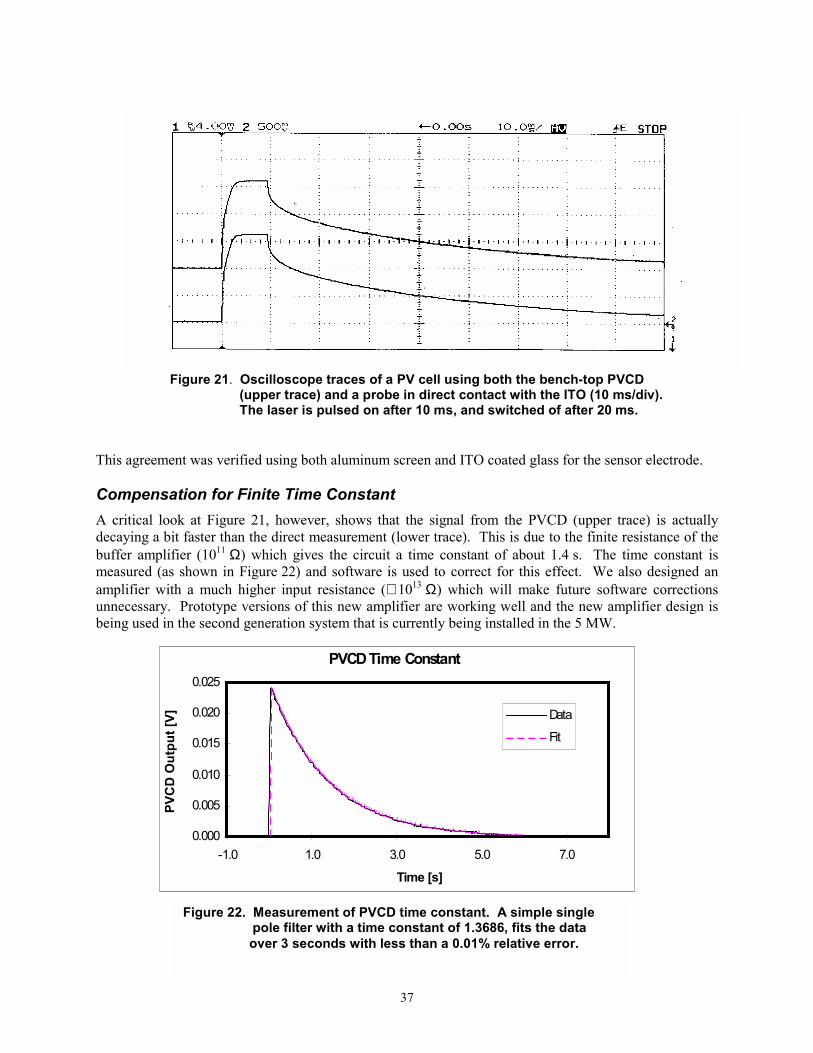
37
Figure 21. Oscilloscope traces of a PV cell using both the bench-top PVCD (upper trace) and a probe in direct contact with the ITO (10 ms/div). The laser is pulsed on after 10 ms, and switched of after 20 ms.
This agreement was verified using both aluminum screen and ITO coated glass for the sensor electrode.
Compensation for Finite Time ConstantA critical look at Figure 21, however, shows that the signal from the PVCD (upper trace) is actuallydecaying a bit faster than the direct measurement (lower trace). This is due to the finite resistance of thebuffer amplifier (1011 Ω) which gives the circuit a time constant of about 1.4 s. The time constant ismeasured (as shown in Figure 22) and software is used to correct for this effect. We also designed anamplifier with a much higher input resistance (≅ 1013 Ω) which will make future software correctionsunnecessary. Prototype versions of this new amplifier are working well and the new amplifier design isbeing used in the second generation system that is currently being installed in the 5 MW.
PVCD Time Constant
0.000
0.005
0.010
0.015
0.020
0.025
-1.0 1.0 3.0 5.0 7.0
Time [s]
PVC
D O
utpu
t [V] Data
Fit
Figure 22. Measurement of PVCD time constant. A simple single pole filter with a time constant of 1.3686, fits the data
over 3 seconds with less than a 0.01% relative error.

38
Measurement Reproducibility
In order for this system to be useful as a diagnostic system, a high degree of reproducibility is needed.Variations come from different sources, such as:
• Changes in the distance, and consequently capacity, between the pick-up grid and the substrate;• Changes in the shunt capacity of the line connecting the grid to the buffer amplifier. A very
significant change can result from a minor perturbation such as bending the coaxial cable betweenthe pick-up grid and the buffer amplifier; and
• Changes in the amplitude of the laser pulse.
All of the above, and other, sources of “signal non-reproducibility” have been and are being investigated.Some of them have been corrected, and other are still being studied and will need software correctionsand active feedback systems. In particular, we measured the stability of the laser and found a largedifference in stability in different lasers. Whereas the IR laser and corresponding PVCD output are stableto within our measurement precision (1 LSB on the digital oscilloscope as shown in Figure 23), we foundthat the red laser, which we are installing in the 5 MW in the second generation device, has amplitudevariations of the order of 5%. A software system will need to be developed in the second year of theprogram to provide active feedback for this system.
Summary of Selected Preliminary MeasurementsFigure 24 shows the output of the PVCD device for cells with the following structures:
• n1, i1, p1, n2• n1, i1, p1, n2, i2• n1, i1, p1, n2, i2, p2
One can clearly see the increase in the PVCD output as more layers are added. One can also observe theprecision to which these PVCD waveforms can be fit to models using only a few parameters. We are nowbeginning the work of correlating these fitting parameter with cell properties measured usingconventional techniques as shown in Figure 25.
Figure 23. Oscilloscope traces of the laser diode moduleCurrent monitor (top) and output of a photodetector(bottom). The oscilloscope recorded the peakvoltages for each of these signals.

39
5 MW 619 A -- From Gas Gates790 nm IR 80 mW 45 mm Laser Beam
0.0
0.1
0.2
0.3
0.4
0.5
-4.0E-04 0.0E+00 4.0E-04 8.0E-04 1.2E-03 1.6E-03 2.0E-03
Time [s]
Lase
r I-M
on [V
]
0.00
0.01
0.02
0.03
0.04
0.05
PVC
D O
utpu
t [V]
Laser N2Laser I2Laser P2PVCD N2- Off Corr'dPVCD N2 - FitPVCD I2- Off Corr'dPVCD I2 - FitPVCD P2 - Off Corr'dPVCD P2 - Fit
Figure 24. PVCD waveforms and fitted curves resulting from a 4-parameter fit.
PVCD Parameters (A1 + A2) vs. VocAmplitude vs Voc IR Laser -- 2 ms scans
R2 = 0.97
0E+00
5E-03
1E-02
2E-02
2E-02
3E-02
0.4 0.5 0.6 0.7 0.8 0.9 1 1.1 1.2 1.3Voc
PVC
D: (
A1 +
A2)
Figure 25. Parameter resulting from fit of PVCD waveform plotted vs.measured open circuit voltage for cell with a differentnumber of layers.
PVCD Amplitude vs. Voc – IR Laser
PVC
D A
mpl
itude
[arb
]
Voc [V]

40
Design of the Second Generation Device for Installation in the 5 MW
Two second generation devices have been designed:
• The first system was designed such that it could be mounted using windows in the gas gates of theproduction equipment. This system has several advantages: (1) there is no worry of contamination;(2) the system can be accessible at all times, even during operations, for modification; and (3)systems can be installed in the gas gates following each of the 3 p-layers to analyze separately eachcell in the triple junction device.
• We designed the second system to be mounted in the vacuum system of the take-up chamberfollowing deposition of all the layers of the triple-junction device. Because this system is separatedfrom the deposition chambers by a gas gate, again the worries of vacuum compatibility areeliminated.
Windows were not initially installed in the gas gates of the 5 MW machine; consequently it would benecessary to remove and re-machine these chambers of this machine to implement the first design; thesecond design, however, could be installed without needed to disassemble the machine, and consequentlyoffered a much lower risk approach.
Although we originally envisioned installing the second generation device in the pilot machine, we haveinstead decided to immediately install it in the production equipment for the following reasons:
1. We believe that this new system may be able to be immediately useful, for example, in alertingthe operator to a serious problem in the system.
2. The production equipment is in operation nearly all the time, whereas the pilot machine is onlyintermittently operated and is frequently off-line for extensive modifications.
3. Consequently, we shall be able to obtain much more data by installing the system in theproduction equipment. Furthermore, all the production material goes through extensive off-lineQA/QC electrical testing that will automatically provide us with data for comparison to the onlinemeasurement.
The hardware for this second generation system has already been installed in the 5 MW take-up chamber,as shown in Figure 26. The electrical hook-up will be completed in the near future.

41
Figure 26. Mechanical schematic showing the mounting of the PVCD in thetake-up chamber of the 5 MW.

42
Task 3 – Development of Reactive Sputtering Process UsingInexpensive Zn Metal Targets for Back Reflector Preparation
Background
An integral part of ECD’s triple-junction solar cell design is the textured metal/ZnO back reflector whichenhances the probability for multiple light passes through the semiconductor absorbing material. Theincreased number of passes increases the chances for light absorption which in turn leads to higher shortcircuit currents and higher cell efficiencies. While the back reflectors are needed in order to achievecertain efficiency goals, the cost of making these materials on the production level is significant. Inparticular, the materials costs exceed those for the semiconductor layer deposition process.
A significant expense in the magnetron sputtering process used to make the back reflectors is the cost ofthe ZnO targets. The cost of these targets alone accounts for over 40% of the total material cost forproducing all of the thin films for the solar modules. Thus, if the ZnO targets could be eliminated fromthe process with a less expensive target, a significant cost savings would result.
Prior to this program, the ECD research team tested a reactive sputtering process which uses a Zn metaltarget in an Ar/O2 atmosphere to create ZnO films for back reflectors. Since the price of Zn metal targetsare 1/5th the price of ZnO targets, and conceivably could be made in-house at an even lower cost, reducedcost was a major incentive to test the feasibility of this process. However, there were other motivations.With the present process, high quality back reflectors are obtainable at production level web speeds.However, at slower speeds (2/3 of the production level speed) back reflectors of even a higher quality canbe obtained due to thicker ZnO layers obtainable at these slower speeds. Thus if higher sputtering ratescould be obtained, the thick ZnO layers and higher quality back reflectors could be obtained at productionlevel speeds. Since higher deposition rates are likely obtainable with the Zn metal target, improvedefficiencies as well as reduced costs may be had with this new process.
Table 5 compares data from this initial feasibility study for single-junction a-Si:H cells prepared withback reflectors (Zn 29 and Zn 33) made using this new deposition process and cells made with backreflector from the 5MW production machine (5MWBR78 and 5MWBR82). The semiconductor layers forall of these cells were co-deposited in the same deposition chamber under deposition conditions whichwere not optimized. ITO and Ag contacts for the cells were also co-deposited in order to minimize anydifferences in the cells other than the back reflector materials. The data for samples Zn 29, 5MWBR78and 5MWBR82 are all the same within experimental error. The Jsc for sample Zn 33 is higher than theother values, however the FF is lower with an overall slight improvement in efficiency. Thus, with littleoptimization it can be concluded from this data that back reflectors can be made using the new reactivesputtering process, having similar quality to those made using the present 5 MW process.
Table 5. Comparison of Data for a-Si:H Cells Co-Deposited on Al/ZnO Backreflectors. Cell Measurements Completed Using AM1.5 Light (Rs is the series resistance).
Sample Voc(V)
Jsc(mA/cm2)
FF Pmax(mW/cm2)
Rs
(ΩΩΩΩcm2)Zn 29 0.952 14.54 0.644 8.91 10.7Zn 33 0.955 15.06 0.638 9.19 11.5
5MWBR78 0.953 14.45 0.647 8.92 11.95MWBR82 0.953 14.30 0.646 8.80 12.5

43
Objective of Backreflector Studies
While the data from the initial studies are encouraging, there are several issues which need to beaddressed before this new process can be incorporated into the 5MW production line. Although some ofthese issues can be addressed using small-scale machines, the process needs to be qualified on ECD’spilot roll-to-roll machine before implementing it in the production facilities.
In this program, we are testing the feasibility of using this reactive sputtering process in a roll-to-rollprocess to verify that it can indeed be used to make long rolls of back reflector coated stainless steel websin production. A pilot roll-to-roll machine is being used to prepare and optimize ZnO layers preparedusing the Zn metal targets. During initial optimization of the deposition conditions, small area cells arebeing fabricated using the new ZnO materials to judge the back reflector quality. Once the quality of theZnO materials using the reactive sputtering process are judged to be similar or better than those madeusing the ZnO targets, 100M lengths of back reflector material will be made to demonstrate that theprocess can be reproducibly used over a long production level length. In the later stages of the program,the processing speed will be increased to a level 1.5 times faster than what is obtained in the 5MWproduction line.
Experimental
In the first year of the program, the reactive sputtering process was optimized in the pilot machine locatedat United Solar (see Figure 27). This roll-to-roll machine is part of United Solar’s decommissioned 2 MWplant and is designed to deposit BR material over a 14 in. wide web. It can be equipped with two Altargets and four ZnO or Zn targets of size 4” x 20”. To optimize the backreflector deposition conditions,the pilot machine was used to deposit thick ZnO layers onto a stainless steel web previously coated with astandard Al layer and a thin ZnO layer using the 5MW production equipment. Depending on thedeposition conditions, Al thin films can have different degrees of texturing which strongly affect thereflection and solar cell properties. In using the Al/thin ZnO coated web made using the 5MW productionline, we were assured that the degree of texturing was similar to that obtained in production and couldthus optimize the thickness and quality of the ZnO layer accordingly to that amount of texturing. The thinlayer of ZnO was used to prevent oxidation of the Al surface during transportation of the web from theproduction machine to the pilot test machine.
To optimize the properties of the ZnO layer, a number of deposition parameters were systematicallyvaried including the substrate temperature, the oxygen and argon flows, web speed and the applied rfpower. Also compared films were made using an Al doped Zn metal target to those made using anundoped target. As a reference, ZnO layers were also made using the standard ZnO targets and the pilotmachine.
To test the quality of the back reflectors, a-SiGe:H nip structures were deposited on 2” x 2” experimentalback reflector coated substrates using the 13.56 MHz PECVD technique and an R&D deposition system.This system has been used to prepare 1 sq. ft. modules with world record efficiencies (>10% stableefficiencies). For each PECVD deposition, nip structures could be deposited on nine different backreflectors. In many of these depositions, high quality back reflectors with the thick ZnO layers made inUnited Solar’s small scale R&D RADLAS system were included for comparison. The back reflectors formost of their world record solar cells and modules were made using this system. The nip structures werethen coated with separate 0.25 cm2 ITO layers for collection. The top contact was completed bydepositing Al grids on top of the ITO layers.

44
Figure 27. United Solar’s roll-to-roll backreflector machine. This machine isalso part of United Solar's decommissioned 2 MW plant and willbe used for the bulk of Task 3, and for part of Task 2.
Cells were characterized using standard IV tests and quantum efficiency measurements. The IVmeasurements were made using AM1.5 light or AM1.5 light filtered using a 610nm low bandpass filter.The filter simulates absorption due to the top and middle cells allowing only red light which reaches thebottom cell in the triple-junction structure. It is important to compare data obtained using the filter due tothe fact that in the high efficiency triple-junction structure, the bottom cell current is the parameter mosteffected by the use of the back reflector. Also using the filter eliminates any fluctuations in the blue/greenlight collection which is affected by a number of conditions unrelated to the back reflector including thequality of the p-layer and the ITO layer.
Results of Work Completed During Phase I of the Program
Web Handling Procedures
Initial experiments were done to determine the effect that air exposure between deposition on the Al/thinZnO structure in the 5MW machine and placement of the coated web into the pilot machine had on thecell properties. Also the thickness of the thin ZnO layer used to eliminate Al oxide formation wasdetermined. Three types of samples were made using the 5MW back reflector (BR) machine: 1) Alcoated stainless steel, 2) same as 1) except with a thin layer of ZnO, and 3) same as 2) except the ZnOlayer is twice as thick. After the 5MW deposition, samples from each of the three types were stored forone month in air or a nitrogen atmosphere. The one month exposure was to simulate the maximum timebetween a 5MW Al/thin ZnO deposition and our experimental ZnO depositions made using the TA2equipment. Using United Solar’s Radlus machine, we have deposited thick ZnO layers on each of thesetypes of samples after the one month of storage to complete the back reflectors. Finally, a-SiGe:H nipcells were deposited on each of the samples to test the quality of the back reflectors and to see which typeof sample we might use to complete our experiments with Zn metal targets.

45
Table 6 compares data for the different cells prepared using the different back reflectors. From this data,it was concluded that:
1) Use of the Al coated stainless steel without any thin ZnO coating led to poor small area cellyields and, for the most part, lower efficiencies.
2) The substrates with 40 and 80 nm ZnO stored in N2 have the best performance in terms of theQuantum Efficiency data (Q.E.) for both the 2 day and 1 month exposure experiments.
3) The 80 nm ZnO substrate stored in N2 has the highest Q.E. current for both the 2 day and 1month exposure experiments.
4) The Q for both the 40 and 80 nm ZnO substrates stored in N2 are similar for both the 2 dayand 1 month exposures showing that the substrates are not changing as a function of time.For all of the other substrates, the Q is lower for the substrates left for 1 month comparedwith those left for 2 days demonstrating that the substrates are deteriorating as a function oftime.
Considering these results, it was concluded that we would use Al/80 nm ZnO substrates and store them inan N2 atmosphere prior to depositing the experimental ZnO layers prepared using the Zn metal reactivesputtering process.
Table 6. Data for Cells Prepared Using the Different Backreflectors After Different Exposure Environments and Exposure Times.
Sample StorageTime BeforeRadlus ZnO
StorageAtmosphere
Before Radlus ZnO
Efficiency(mW/cm2)
Voc(V)
FF IntegratedQ.E. Current
(mA/cm2)Std 5MW
BackReflector
- - 2.62.52.5
0.5980.5990.601
0.5830.5870.585
7.747.517.62
5MWAl only
2 days Air 2.2 0.572 0.472 8.10
1 month Air All Devices Shorted
5MWAl/ 40nm
2 days Air 2.5 0.588 0.506 8.82
ZnO 1 month Air 2.6 0.598 0.600 7.45
5MWAl/80nm
2 days Air 2.5 0.575 0.526 8.79
ZnO 1 month Air 2.6 0.611 0.559 8.01
5MWAl only
2 days N2 All Devices Shorted
1 month N2 2.5 0.570 0.546 8.28
5MWAl/ 40nm
2 days N2 2.7 0.585 0.531 8.76
ZnO 1 month N2 2.9 0.577 0.572 8.89
5MWAl/80nm
2 days N2 2.8 0.574 0.533 9.67
ZnO 1 month N2 2.8 0.579 0.562 9.44

46
Reactive Sputtering Optimization
During optimization of the cells made using the ZnAl(5%) metal targets and the reactive sputteringprocess, a number of different deposition conditions were tested. Of the deposition parameters varied, theoxygen flow had the greatest effect on the cell properties, as one might expect. In particular, the oxygenflow strongly affected the short circuit current (Jsc) of the cells as is shown in Figure 28. Between oxygenflows of 40 and 70 sccm, the Jsc value increases by around 0.5 mA/cm2. Further increases in the oxygenflow leads to no increase in Jsc. Also demonstrated in the figure is the fact that the substrate temperaturehas little effect on the Jsc. As can be seen from the data in Table 7, the average fill factors are slightlylower fill factors are obtained when the oxygen flow exceeds 90 sccm.
6.5 6.7 6.9 7.1 7.3 7.5 7.7 7.9 8.1
30 50 70 90 110 130 150 170 190 Oxygen Flow (sccm)
Jsc
(mA
/cm
2)
Jsc(Ts=100) Jsc(Ts=250) Jsc(Ts=320)
Figure 28. Dependence of Jsc for a-SiGe:H cells on oxygen flow. (Ts=substrate temperature)
Table 7 lists cell data for a number of cells whose ZnO layers were prepared under a variety of conditions.Parameters such as the Ar flow, the target current and the substrate temperature had little effect on the cellproperties as can be seen from the data listed in the table. Also in the table are data for a cell made usingjust the Al/thin ZnO as the back reflector adding no additional ZnO layer using the reactive sputteringprocess. It is clear that the properties for this cell are inferior to those for the cells made with theadditional ZnO layers demonstrating that properties for the cells are affected by the added ZnO layer.
Besides using the 5% Al doped Zn target, we also fabricated cells using a 3% doped target and anundoped target in the pilot machine. Table 8 compares cells made in the same nip deposition with backreflectors made using these three different sputtering targets. In terms of both cell properties and plasmastability, it does not matter whether the 3% or 5% Al target is used. In contrast, use of the undoped targetled to poorer cell performance with the fill factors being significantly lower. In addition, opticalmeasurements of the plasma demonstrated that the plasma with the pure metal target varied as a functionof time. Specifically, the Zn plasma signal increases as does the sputtering target voltage with increaseddeposition time. Use of higher oxygen flows improves the plasma stability, however the plasma can notmaintain the stability achieved with the doped targets. It is not yet known whether the lower FF are

47
associated with these plasma instabilities, however it is clear that use of the doped targets does lead to amore manageable process.
Table 7. Data for a-SiGe:H Cells Prepared with Backreflectors Made Using Reactive Sputtering Technique Under a Variety of Deposition Conditions.
Substr.Temp.(°C)
O2Flow
(sccm)
ArFlow
(sccm)
TargetCurrent(amps)
Voc(V)
Jsc(mA/cm2)
FF Rs
(Ωcm2)Pmax
(mW/cm2)
250 40 30 8 0.723 7.11 0.684 11.9 3.5250 40 30 8 0.725 7.31 0.685 11.9 3.6250 45 30 8 0.723 7.34 0.684 11.6 3.6250 50 30 8 0.726 7.12 0.676 11.6 3.5250 70 30 8 0.726 7.54 0.675 12.0 3.7250 90 30 8 0.730 7.78 0.681 12.7 3.9250 100 30 8 0.728 7.78 0.664 12.9 3.8250 120 30 8 0.723 7.69 0.669 11.2 3.7100 70 30 8 0.726 7.61 0.679 11.5 3.7250 70 30 8 0.729 7.69 0.676 10.9 3.8320 70 30 8 0.734 7.77 0.671 12.1 3.8320 70 30 6 0.724 7.79 0.671 13.9 3.8320 70 30 8 0.734 7.77 0.671 12.1 3.8320 70 30 10 0.728 7.65 0.674 14.0 3.8250 90 10 8 0.726 7.78 0.674 12.7 3.8250 90 30 8 0.729 7.78 0.681 12.7 3.9250 90 50 8 0.732 7.69 0.678 11.2 3.8No
AddedZnOlayer
- Only Al/thinZnO
0.701 6.86 0.683 11.5 3.3
Table 8. Data for a-SiGe:H Cells Whose Backreflectors were Made Using Targetswith Different Al Contents.
TargetMaterial
Voc(V)
Jsc(mA/cm2)
FF Rs
(Ωcm2)Pmax
(mW/cm2)ZnAl (5%) 0.715 7.83 0.667 11.5 3.7ZnAl (3%) 0.718 7.76 0.676 12.1 3.8
Zn 0.712 7.81 0.643 16.2 3.6
To truly judge the quality of the back reflectors made using the new reactive sputtering process, single-junction a-SiGe:H cells were made using three different types of back reflector listed below:
1) back reflectors made in the pilot machine under the optimized conditions using theexperimental reactive sputtering process and the ZnAl(5%) sputtering targets,
2) back reflectors made in the pilot machine under the optimized conditions using the standardsputtering process and ZnO targets,
3) back reflectors made in the 5MW production machine using the standard sputtering processand ZnO targets.

48
Again, the nip structures for all three types of back reflectors were made in the same deposition run usingUnited Solar’s 1 sq. ft. R&D deposition system. The data for the three types of cells are listed in Table 9.Comparing data for the cells made using the back reflectors from the pilot machine, the cell properties forthe cells made using the ZnAl (5%) targets are similar to those for the cells made using the ZnO targetsdemonstrating that the new reactive sputtering process can be used to prepare high quality back reflectormaterial.
Table 9. Data for a-SiGe:H Cells Whose Backreflectors were Made with the Reactive Sputtering Process Using Zn Metal Targets and the Standard Process Using ZnO Targets.
TargetMaterial
BR Machine Voc(V)
Jsc(mA/cm2)
FF Rs Pmax(mW/cm2)
ZnAl(5%) Pilot Machine 0.731 7.57 0.668 10.7 3.7ZnO Pilot Machine 0.731 7.49 0.665 12.0 3.6ZnO 5MWProduction 0.730 7.42 0.662 13.2 3.6
As a final comparison of the back reflectors made with the Zn metal and ZnO targets, we have fabricatedlarger area (44.5 cm2) single-junction a-SiGe:H cells using the two types of back reflectors. The nipstructures for the two cells were prepared in the same deposition run in order minimize the differencesfrom layers other than the ZnO materials. Table 10 displays data for these two types of cells. The slightdifferences in the properties for the two cells are within experimental error again demonstrating that theinexpensive ZnAl(5%) targets can be used to prepare high quality back reflector material. These cellsfulfill the required deliverable D-1.4.9.
Table 10. Data for 44.5 cm2 Modules Made with Different Backreflectors.
TargetMaterial
BR Machine Jsc(QE)(mA/cm2)
Voc(V)
FF Rs
(Ω/cm2)Efficiency
(%)ZnAl(5%) 2 MW
Pilot18.9 0.77 0.631 0.20 9.18
ZnO 5MWProduction
18.5 0.77 0.649 0.18 9.24
Preparation for Tests in 5MW Production Machine
Having established that the reactive sputtering process can be used in the roll-to-roll design to make highquality ZnO layers, we are now making arrangements to fabricate a 100m long back reflector coated webto demonstrate that the process can be used to make the high quality material consistently over a longperiod of time, a requirement for production. At the beginning of this program, it was thought that thefabrication of the back reflector for this 100m long section of web would be done using the pilot machine.However, in order to expedite the implementation of the new sputtering process into production, we havedecided to complete this test using the 5MW production equipment. In order to do this, we have madeseveral preparation steps during this phase of the program including the purchase of six production sizeZnAl (5%) targets, the changing of cathode shielding in the production machine and the purchase, atECD’s expense, a mechanical pump and blower capable of handling oxygen. We are presently waitingfor the delivery of the pump and blower that is scheduled to occur in mid July. Shortly after delivery(August), we will begin depositions in the 5MW facility using the reactive sputtering process.

49
Plans for Phase II of the Program
In the next year, we plan to optimize the reactive sputtering process in the 5MW production plant to allowfor the fabrication of a 100M long section of solar module material using the new process to prepare theZnO layer. Since the optimized conditions in the production machine may differ from those for the pilotmachine, this optimization process will include systematic variation of the Ar and O2 flows, the webtemperature and the applied power. We will also test the use of the new process to prepare the Znmaterial at the Al surface. Thus far, we have only used the new process after a thin ZnO layer has beendeposited on the Al using the standard sputtering process and ZnO targets. Once small area cells havebeen fabricated using the small area equipment and the expected high efficiencies are achieved, a fullscale 600M production run will be completed using the new sputtering process and all of the productionequipment. This will include the deposition of triple-junction nip structures using the 5MW depositionmachine. Using this material, standard QA/QC coupons will be fabricated and the sub-cells qualitycompared with that for the standard production sub-cells made using the standard sputtering process.

50
Task 4 - Cathode Hardware Studies for a-Si(Ge):H i-layer Depositions
Background
Efficiencies for small area a-Si:H based devices are being steadily increased; the present world record is13% stable efficiency for a small area triple-junction cell (0.25 cm2 active area) produced in a small scalereactor (4” x 4” maximum deposition area) by United Solar. This accelerating improvement suggests thateven higher efficiencies should be obtainable. However, the efficiencies obtained for large area solarmodules are still significantly lower than the 13% values being near 8-9%. The lower module efficienciesare due in part to back end processes such as lamination and module designs. However, even the smallarea cells fabricated in the large area, continuous roll-to-roll machines (in particular the 5 MW machine)have yet to demonstrate efficiencies that match the world record values even though thoroughoptimization studies have been carried out. This suggests that there are inherent problems with thepresent large area process and/or hardware designs that limit the efficiencies to their present day values.
One problem which is more difficult to achieve in the present large area production machines ascompared with the smaller R&D machines is the ability to prepare reasonably uniform film depositionsacross the entire cathode area during PECVD depositions. This problem was of major concern during ouroptimization program for the 5 MW production machine. For example, a-SiGe:H i-layer depositions, inorder to obtain relatively uniform film depositions across the length of the cathodes for each vacuumchamber, we were limited to work in a small area of deposition parameter space. If parameters outsidethis space were used, gradients across the length of the cathode were obtained for the Ge content as wellas for the deposition rate as is shown in Figure 29 It was found that these non-uniformities were notrelated to unequal power distributions across the cathode or gas depletion, as one might expect. With amoving web substrate, this affect lead to cells and modules which had significant variations in the Gecontent through the depth profile of the a-SiGe:H i-layers. Variations in the bandgap of the materialsobviously accompanied the Ge content fluctuations that likely formed shallow carrier traps in the i-layerslimiting the carrier collection and cell efficiencies. Also, since the quality of a-Si:H based materialsprepared by the PECVD method depend strongly on the film deposition rates, the variations in thedeposition rates led to the formation of high quality material in the region of the cathode where thedeposition rates were low and poorer quality material in the region where the deposition rates were high.Under these conditions, the overall film and device performance was limited by the poor materialproduced in the high deposition rate region. If the overall deposition rate were lowered in order toimprove the material produced in the high deposition rate region, the machine throughput wasunacceptably low.
We should note that similar variations in the deposition rates across the lengths of the cathode were alsoobserved for a-Si:H layers. Thus the non-uniformity problem was not related to differences in thedecomposition rates of Si and Ge source gases but instead is inherent to the existing vacuum hardwaredesign.
When limited to a small region of parameter space, the efficiencies are likely limited to low values. Witha different internal hardware design that allows for uniform depositions across a large area of parameterspace, the maximum efficiency would likely be outside the small area of parameter space we are presentlyrestricted to. Thus, if such a deposition hardware design could be devised, higher cell and moduleefficiencies would likely be obtained.

51
Moving Web
Cathode
Ge content 17% 20% 32%
Relative 18% lower Std. 42% higherDep. Rate than Std than Std
Figure 29. Variation of Ge content and deposition rate across cathode.
In attempting to achieve the record high efficiencies using the large machines, one must be assured thatthe film growth conditions used to prepare the large modules are similar to those obtained using the smallarea machines. In particular, the plasma chemistry, electrical potentials and film surface growthconditions must be duplicated in order to prepare the proper film quality and film microstructure.Specifically, a deposition system which comes close to replicating the plasma densities for all of the Sibased radicals and H atoms in the plasma, the substrate self bias and the plasma potential, and the electronand ion bombardment of the growth surface must be designed. Only when this is done will one have thepotential of achieving the high efficiencies with the large area systems. While the present internalhardware design for the 5MW chambers is not dramatically different from the design for the small scalesystems used to prepare the high efficiency cells, a design for the large area chamber internal hardwarewhich more accurately reproduces the small scale geometry might lead to higher large area cellefficiencies.
Objective of Cathode Hardware Studies
In this program, we will develop new internal hardware for the i-layer deposition chambers used inUnited Solar’s 5MW production line in order to improve the quality and uniformity of these materials toincrease the overall solar cell and machine efficiencies. Three newly designed cathodes will be built,tested and compared with the 5MW design during this three year program. To judge the usefulness ofeach design, single-layers are being made to test the ability to obtain uniform deposits over large areasand large regions of deposition parameter space while single-junction a-Si:H cells are being fabricated totest the quality of the deposited layers. Each design is first tested in a single chamber system with a staticsubstrate.
Once final designs for the internal hardware are completed, the hardware is to be incorporated into anexisting chamber on the 2 MW pilot semiconductor line at United Solar (see Figure 30). To test this newinternal hardware, single-junction nip a-Si:H cells will be prepared using the new hardware on a movingweb substrate. The i-layer conditions will be optimized for the highest FF for cells with similar Jsc values.Improvements in the hardware will be judged by increased FF for the cells and improved depositionuniformity over those obtained with the 5MW style cathodes. If necessary, alterations to the systemhardware will be made so that the plasma and growth conditions more closely match those for the smallarea R&D system. Also, temperature, gas flow and pressure distributions throughout the chamber will beclosely monitored. If it is demonstrated that this new design is an improvement over the presently useddesign, we will incorporate the new chamber design into the 5MW production line.

52
Figure 30. Double-junction roll-to-roll plasma-CVD processor, previously used as United Solar’s production machine. This machine will be used as an experimental machine for much of the work proposed in Tasks 1 and 4.
This roll-to-roll PECVD processor was used as a solar cell production machine when United Solar’sproduction plant had a capacity of 2 MW. It is capable of making nipnip tandem solar cell structures on a14” web. The i-layer cathode lengths vary from 17” to 56” long.
Experimental
Thus far, we have developed three new cathode designs and have tested one design with the testing oftwo others in the later stages of the program. The new designs will incorporate several ideas that weredevised during the 5MW machine optimization program, during which a great deal of knowledge wasobtained. Further studies of the 5MW cathode design in this program has also proved beneficial towardsthe development of this new hardware. Incorporation of several improvements should lead to bettercontrol of the gas flow, temperature distribution and film uniformity across the cathode and depositionarea.
Initial tests of the cathodes are being completed using a single test deposition chamber (see Figure 31) inwhich two different styles of cathodes can simultaneously be compared in the same environment. Duringthis first year, we designed, built and compared one new cathode design with a cathode that mimics thedesign used in 5MW production machine. In the same system pump-down, single layer films to testdeposition uniformity and/or i-layers for nip solar cells to test i-layer quality were made from both typesof cathodes.

53
Typically, the same deposition conditions were used for both deposits including the same rf powerdensity. For the single layer deposits on bare stainless steel substrates, film thickness across thedeposition area was measured using standard optical techniques. The 13.56 MHz Plasma EnhancedChemical Vapor Deposition (PECVD) technique is being used to deposit all of the materials.
Cathode Design #1 Cathode Design #2Viewport
Figure 31. Single chamber system used for cathode development.
To fabricate 0.25 cm2 a-Si:H single-junction test cells, the cathode hardware to be tested is only beingused to prepare the i-layer materials. Preparation of both the intrinsic layer and the doped layers in asingle chamber system is not desirable because of the cross contamination effects which hinder electronand hole collection in the cell. Therefore to make the cells for this study using the single chamber system,we are making the n- and p-layers by the PECVD method in a separate, proven load lock R&D system.This system has prepared high efficiency triple-junction devices in the past and is presently used to makehigh efficiency single junction cells. The steps we will use to prepare each of the devices are as follows:
1) deposit an a-Si:H:P n-layer using the load lock system,2) quickly transport the n-layer coated substrates to the single chamber system attempting to minimize air exposure,3) deposit i-layers using the two different cathode designs,4) quickly transport the n/i coated substrates from the single chamber system to the load lock system again attempting to minimize air exposure,5) deposit an a-Si:H:B p-layer using the load lock system,6) deposit ITO/Al contacts using standard evaporation techniques.
Such a device is depicted in Figure 32. For these studies, we will focus on cells made without currentenhancing Ag/ZnO backreflectors to minimize the complexity of the cells.
ITOp-layer (13.56 MHz )
i-layer (13.56MHz)
n-layer (13.56 MHz)stainless steel substrate
Al contacts
Figure 32. a-Si:H single-junction cell structure.

54
In the pilot machine, all three semiconductor layers (n-, i- and p-layers) are being deposited in the roll-to-roll process. Again, these layer are being deposited on bare stainless steel substrates. ITO contacts aredeposited using a dc sputtering technique and a 1 sq. ft. R&D machine while Al contacts are evaporatedonto the ITO using a small scale reactor.
To characterize the devices, current vs. voltage (IV) measurements are made to obtain standard solar celldevice parameters (short circuit current (Jsc), Fill Factor (FF), Open Circuit Voltage (Voc), etc.). Also,quantum efficiency measurements are also used to obtain integrated currents and determine collectionlosses in cell.
After initial cell measurements, the devices are being subjected to light soaking periods. We are first lightsoaking the samples for 10 and 30 hrs. under AM1.5 light at 50ºC, after each of these periods measuringthe cell properties. To measure the stable efficiencies, one must light soak them for 600 hrs. But to getpreliminary data on how the deposition parameters are affecting the amount of degradation, we aremaking these limited light exposure measurements to optimize the deposition conditions for minimumdegradation and optimum stable cell efficiencies. After initial screen testing, we are selecting certaincells for long term light exposures to obtain accurate values for the stable efficiencies.
Results of Work Completed During Phase I of the Program
The 5MW Style Cathode in the Single R&D Chamber
Testing Similarity to Cathodes Used in Production
Initially, several depositions were completed to verify that the 5MW style cathode in the single R&Dcathode testing chamber behaved similar to the cathodes in the 5MW production machine. In particular,we were testing to see if the non-uniform deposits across the length of the cathode would be obtained atthe production level deposition rates. Figure 33 compares deposition rate profiles across the length of thecathode obtained using different deposition conditions and the 5MW style cathode. These profiles weretaken near the center of the deposit and the cathode as is shown in Figure 34. In Figure 33, we compareprofiles taken at different applied power levels that led to different deposition rates while all otherdeposition parameters were nominally fixed. The average deposition rates in Å/s for each profile is listedin the figure legend in brackets. As is the case for the production line cathodes, as the power level isincreased, the film thickness, and thus the deposition rate, near the gas inlet becomes much larger than thethicknesses obtained near the pump out port. This variation in deposition rate across the cathode length ispartially due to a gas depletion effect but can not be the only cause due to the fact that there is not a dropin deposition rate near the pump out side of the cathode as the power is increased. This trend of pooreruniformity with increased power was the same effect observed during the optimization of the 5MWproduction line.

55
0
1
2
3
4
5
0 10 20 30 Distance From Cathode Edge
Near Gas Inlet (in.)
Dep
ositi
on R
ate
(A/s
)
Low Power Mid Power High Power
Figure 33. Thickness profiles for films made at different applied rf powers.
Top View
Stainless SteelSubstrate
Cathode UnderneathSubstrate
Line along which film thicknesses were measured
Cathode
Side View
GasInlet
Stainless SteelSubstrate Pump
Out
Figure 34. Orientation of film thickness measurements.
In these studies, it became obvious that the uniformity of the deposit across the cathode length wasprimarily dictated by the applied power level as it was for the cathodes in the production line. Figure 35displays the degree of uniformity across the length of the cathode as a function of deposition rate. As afigure of merit for the film uniformity, the y axis in this figure denotes the difference between themaximum and minimum deposition rates obtained across the length across the cathode divided theaverage deposition rate for the deposit. The differences in applied power are denoted by the differenticons. As can be seen from the figure, at each fixed power level, the degree on uniformity remainsrelatively unchanged while other deposition parameters including the hydrogen flow, the active gas flow(silane), and the substrate temperature were altered changing the deposition rate. In contrast, theuniformity becomes poorer with increased the power.

56
20 40 60 80 100 120 140 160
0 1 2 3
Avg. Deposition Rate (A/s)
100
*(M
ax -
Min
)
Avg
Dep
Rat
e
Low Power Mid Power High Power
Figure 35. Variation of deposition uniformity over length of cathode as a function of deposition rate.
From the data in Figure 35, one can observe that fairly uniform deposits and relatively high depositionrates (greater than 2 Å/s) can be obtained at low power levels (80-120W). However to achieve theserates, low hydrogen dilution levels and high silane flows had to be used which led to polysilicon powderformation on the cathode leading to poor cell performance. This is shown in Table 11 where data for a-Si:H cells whose i-layers were made at the same rates but different applied powers are compared. Thecell whose i-layer was made using the low power and less hydrogen dilution has significantly poorer FFand solar cell efficiency (Pmax). Thus the poor cell performance eliminates the possibility of using the lowpower/low dilution conditions to obtain good deposition uniformity.
Table 11. Data for a-Si:H cells made at different applied powers but similar i-layer deposition rates.
Power(W)
i-layerDep. Rate
(Å/s)
Voc(V)
Jsc(mA/cm2)
FF Rs
(ΩΩΩΩcm2)Pmax
(mW/cm2)
120 1.80 0.949 10.93 0.577 16.7 5.99180 1.85 0.928 10.61 0.659 9.9 6.49
From the these results, it was clear us that in terms of deposition uniformity across the length of thecathode, this cathode behaves similarly to the cathodes in production in that at increased deposition rates,the deposits are either non-uniform or of poor quality.
Attempts to Improve Uniformity Using 5 MW Style Cathode
In an attempt to better understand the causes for the non-uniform deposits at high rates, slight alterationsto the 5MW cathode design were studied. In one case, we altered the pumping manifold to see if thepumping geometry would strongly affect the deposition uniformity. In particular, it was thought that theuniformity across the width of the substrate (cathode) could be improved through an alteration of the gasflow pattern. After four alterations to the pumping manifold, no significant change in the uniformity wasobserved.

57
In terms of the uniformity across the width, it was also discovered in these studies that excess hydrogengas from a source outside the cathode hardware and gas manifold, such as from our proprietary gate gates,does significantly affect the deposition uniformity. This is demonstrated by the data shown in Figure 36where the deposition rate profiles across the width of the cathode is shown for different outside gas flows.Comparing the profile when hydrogen gas flowed with the profile when no outside gas flowed, there is asignificant drop off in the deposition rate and thus the film thickness when hydrogen gas flowed. Thethinner films lead to lower efficiencies for the subcells on the edges of the film and for the 12” widemodules. However, by adding a small amount of silane to the outside hydrogen gas flow, one can onceagain obtain the desired uniformity across the web as is shown in the figure. This result can immediatelybe applied to the 5MW production line, in particular to the gas gate flows, to improve the depositionuniformity across the width of the web.
1
1.2
1.4
1.6
1.8
2
0 5 10 15Distance across width of substrate (in)
Dep
ositi
on R
ate
(A/s
)
no gas flowH2 gas flowSiH4+H2 gas flow
Figure 36. Uniformity across width of web (cathode) from deposits made using different gas flows from outside cathode and gas manifold hardware.
Use of pulsed rf plasmas was also tested as a method to improve the deposition uniformity across thelength of the cathode. It was thought that by using short, high decomposition rate pulses, one wouldminimize radical interaction that may be a chief cause for the non-uniform deposits at high rates. Severalexperiments were completed using different duty cycles, pulse widths, and no-pulse power levels. In eachcase, more uniform deposits but lower deposition rates were obtained when the pulsed plasma was usedinstead of the continuous constant power conditions. Also, powder formed on the cathode each time apulsed plasma was used leading to lower cell efficiencies. The source of this powder is not yetunderstood. Alteration of the gas flows and applied powers to match the deposition rates obtained usingthe continuous power conditions led to increased powder formation. Thus, use of pulsed power is not theanswer to obtaining uniform deposits and we have still yet to find a method to obtain uniform depositsacross the length of the cathode using the 5MW production hardware.
Testing of New Cathode Design in the Single R&D Chamber
One new cathode design has been thoroughly tested in the single chamber cathode testing system alongwith the 5MW style cathode. For each system pump down, separate deposits were made using bothcathodes under similar gas flow conditions, substrate and cathode temperatures, power densities andchamber pressures. This new cathode has several features which mimic those for cathodes used in R&Dwhich produce cells of high efficiencies. In particular, this new cathode differs from the 5MW style

58
cathode in terms of gas flow pattern and electrical potentials obtained during deposition, including thesubstrate self bias.
A number of deposits were made using both types of cathodes with the following deposition conditionsvaried; the substrate temperature, the cathode temperature, the applied rf power, and the silane andhydrogen gas flows. For each deposit, a large substrate was used for characterization of the depositionuniformity while 2”x2” n-layer coated substrates were also included for cell preparation and judgement ofthe i-layer quality.
It was found that with this new design, one could obtain uniform deposits (±8%) over the entire cathodearea at a wide range of deposition rates (1-5 Å/s) using a number of different deposition conditions.Figure 37 displays uniformity profiles across the center of the cathode hardware for typical low rate andhigh rate deposition condition. One should note that the new cathode is roughly half as long as the 5MWcathode design. However, our engineers and scientists have determined prior to the construction of thiscathode that because of the cathode’s unique design, expansion of the cathode to twice it’s present sizewill not cause a significant alteration of the deposition profile. The ability to obtain good uniformity overthis relatively wide range of deposition rates is likely associated with the different gas distribution systemfrom the 5MW cathode design. This is a significant improvement over the production style cathode.
0123456
0 2 4 6 8 10 12Distance across cathode length (in.)
Dep
ositi
on R
ate
(A/s
)
Low Rate (1.7A/s)High Rate (5.1A/s)
Figure 37. Deposition rate profiles across new cathode at different deposition rates.
In terms of i-layer quality, a number of cells were made as can be seen from the data shown in Figures 38and 39. In the figures, the fill factor (FF) and maximum power (Pmax), or cell efficiency, are plotted as afunction of short circuit current. Both the fill factor and the cell efficiency depend strongly on the i-layerthickness. For these a-Si:H cells, the short circuit current depends almost linearly with film thickness inthe range of Jsc studied. Thus, the figures roughly contain the trends of FF and Pmax with i-layer thickness.To compare cells in this case i-layer quality, one should compare cells with the same i-layer quality andthus the same Jsc value. Of course during optimization of the deposition conditions, most of the cells werenot made under the optimal conditions (the solid circles in the figures). For both types of cathodes, it wasdetermined that i-layers made with high hydrogen dilution of the plasma and a substrate temperature of225 ºC had, on average, the best cell properties. In the figures, the data for these cells are denoted byopen triangles and open circles for the new and 5MW style cathodes, respectively. Under theseconditions, the cells made using the new cathode had significantly poorer performance than the cellsmade using the standard 5MW cathode due to lower FF. This can be seen more clearly from the datashown in Table 12 where values for cells with similar i-layer thicknesses made under the optimal
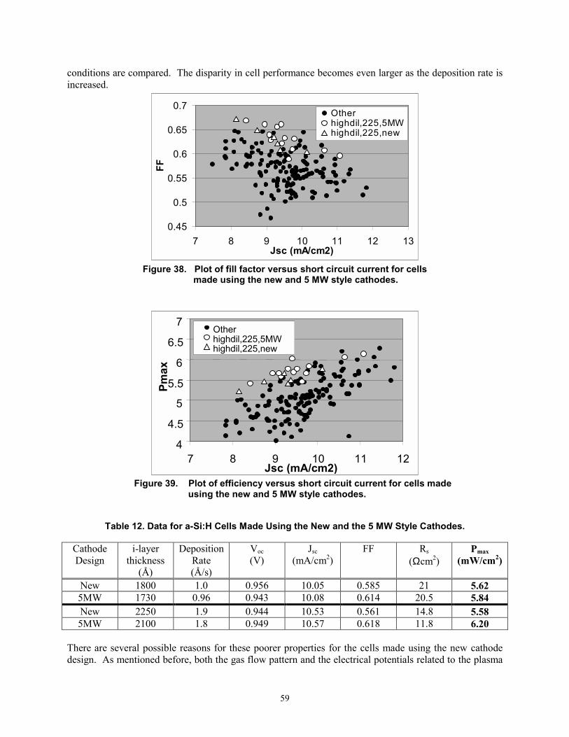
59
conditions are compared. The disparity in cell performance becomes even larger as the deposition rate isincreased.
0.45
0.5
0.55
0.6
0.65
0.7
7 8 9 10 11 12 13Jsc (mA/cm2)
FF
Otherhighdil,225,5MWhighdil,225,new
Figure 38. Plot of fill factor versus short circuit current for cells made using the new and 5 MW style cathodes.
4
4.5
5
5.5
6
6.5
7
7 8 9 10 11 12 Jsc (mA/cm2)
Pmax
Other highdil,225,5MW highdil,225,new
Figure 39. Plot of efficiency versus short circuit current for cells made using the new and 5 MW style cathodes.
Table 12. Data for a-Si:H Cells Made Using the New and the 5 MW Style Cathodes.
CathodeDesign
i-layerthickness
(Å)
DepositionRate(Å/s)
Voc(V)
Jsc(mA/cm2)
FF Rs
(Ωcm2)Pmax
(mW/cm2)
New 1800 1.0 0.956 10.05 0.585 21 5.625MW 1730 0.96 0.943 10.08 0.614 20.5 5.84New 2250 1.9 0.944 10.53 0.561 14.8 5.585MW 2100 1.8 0.949 10.57 0.618 11.8 6.20
There are several possible reasons for these poorer properties for the cells made using the new cathodedesign. As mentioned before, both the gas flow pattern and the electrical potentials related to the plasma

60
are different in this new design. While the flow pattern and the potentials set up by the plasma can affectthe i-layer quality, previous experience with different deposition reactors suggests that in this case, thedifferent gas flow pattern in not likely the cause. Instead, we believe the electrical configuration is moresuspect. It was also observed that powder formation occurred more easily in this cathode configurationthan with the 5MW style. Build-up of this porous powder material can lead to absorption of water vaporduring venting and air exposure of the deposition system. This water vapor can later lead to oxygenincorporation in the i-layers and poor cell performance. This increased powder formation could be aresult of the gas flow pattern or the electrical configuration. If this is the case, this may be a signal thatthe plasma associated with the new design contains more complicated Si based radicals which lead to theformation of polysilicon chains. However, we believe that it is for the most part related to complicateddesign which leads to the exposure of colder surfaces to depositing species.
The experience gained during the study of this first new cathode design has led to the engineering of asecond configuration. This design has a similar gas flow pattern to the first new design and thus weexpect the deposition uniformity will be as equally good. Electrically and geometrically, this seconddesign is more similar to the 5MW design and, thus, the cell properties and the i-layer quality should beimproved over the first new design. This design has recently been built and will be installed into thecathode testing system during the early part of phase 2 of the program.
Establishment of Baseline “5MW-like” Cathode in Roll-to-Roll Pilot Machine
During this period of the program, we have also begun work for testing of the new cathode designs in theroll-to-roll pilot system for the moving web testing. This machine is equipped with cathodes similar tothose used in the 5MW production machine and initially these cathodes will be used to set a baseline forthe machine. This machine has not been in use for over three years and was thus in need of severalrepairs. A list of some of the repairs completed during this reporting period are listed below:
• Servicing and repair of five rf power supplies• Installation of a complete new pressure monitoring system• Full repair of the web drive system• Repair of eight heating controls• Reconfiguration of the gas handling system• Extensive repair of the gas scrubber system• Extensive repair of three of the five mechanical pumps• Installation of a new nitrogen purge system for the exhaust gases• Repair of a number of safety interlocks• Complete replacement of the exhaust manifold for the mechanical pumps• Complete replacement of Ar o-ring purge lines
The list was much more extensive then we initially thought when the program started. However,completion of the repairs was done at the end of this first phase of the program. Setting the baseline forthe machine will begin at the beginning of phase 2 of the program.
Plans for Phase II of the Program
In the next year, we will focus on developing a second new style of cathode. This style has a gas flowpattern similar to the cathode first tested, but electrostatically similar to the 5MW style cathode.Eliminating the difference in electronic potentials between the new style cathode and the 5MW stylecathode should lead to cell efficiencies similar to those obtained with the 5MW cathode. The improveddeposition uniformity should come with the use of a different gas flow pattern from the 5MW style

61
cathode. The hardware for this cathode has been made and installation into the cathode testing singlechamber should begin shortly. Thorough testing will be made of the deposition uniformity and i-layermaterial quality through systematic variation of a number of deposition parameters.
Final preparations of the roll-to-roll pilot machine have just recently been completed and plans fordeposition runs in the month of July are now being made. The first set of runs will be made using the5MW style cathode to set a baseline with a new cathode design tested soon after.
Modeling for Amorphous Silicon Deposition
Introduction
In the first year of this program the major accomplishment was to convert a Boltzmann code, previouslydeveloped for simulating diamond deposition, chlorine etching, and oxygen ashing in plasma reactors, toa code appropriate for modeling the plasma assisted deposition of amorphous silicon. An importantcomponent of this involved determining which neutral and ion gas species are needed to accuratelysimulate the gas chemistry. In addition, a crude model, appropriate for a one-point code, wasincorporated to model diffusion to the walls and silicon deposition. The code was then debugged and runusing conditions appropriate to a specific reactor run and the predictions of the code were compared todata. Comparisons with the thickness of the deposition at the center of the substrate showed goodagreement. As a one-point code this simulation is incapable of showing either the effects of sheaths, andhence ions, at the walls or the effects of non-uniformity in the electric field, which can lead to non-uniformity in the deposition. To begin to address these issues we also adapted a 1D RF code to thisproblem and this code has been tested. Now that the Boltzmann code has been validated against data itwill be run for a variety of electric field parametric values to generate a table of electron energydistributions and neutral densities appropriate to each value of the local electric field. These tabularvalues will be inserted in the RF code to generate predictions of sheath structure and ion dynamics. Whenthis code is validated a 2D version will be constructed to more accurately account for neutral diffusioneffects. These tools will provide a reliable means of simulating the major physical effects in the reactor.
Simulation Strategy
Simulating an RF system involves an analysis of local and global phenomena. In the pressure regimeappropriate for the ECD reactor, these phenomena de-couple. On the global level we can write continuityequations for electron, ion, and neutral species particles and momentum. These equations treat eachspecies as a fluid and do not solve for the velocity space distribution functions of the species. Thecontinuity and momentum equations for each species would be an exact description of the system if weknew the pressure tensor. This however involves solving an unending chain of higher order momentequations. Fortunately, for the case at hand we are able to make simple and accurate assumptions as tothe form of the pressure tensor for each species in terms of the species density.
The continuity equation for the electron and ion momenta requires a knowledge of the electric fielddistribution, which for this frequency range can be derived from the electrostatic potential. The potentialis obtained by solving Poisson’s equation given the electron and ion densities. Thus far all of thequantities required are global quantities, which involve solving equations on the scale of the reactor.However, the solution of the various continuity equations depends on local processes as well. Some ofthese involve neutral kinetics: neutral species A and B interact to form neutral species C and D. Othersinvolve electron mediated processes: an electron impacts molecule A and produces molecules B and C, oran electron impacts species A and knocks off an electron producing an electron- ion pair.

62
While the neutral-neutral interactions can be obtained from kinetic rate information, calculating theelectron rates for electron-neutral processes involves solving for the electron distribution function. Thesolution depends on the value of the electric field during the entire history of the particle. In low pressuresystems this requires a global solution since electrons at one point may have been heated by electric fieldsat another spatial point at and earlier time. At the higher pressure of the ECD reactor, electrons moveonly a short distance in space during a typical heating time due to the short mean free path. Therefore theelectron energy distribution function depends only on the local value of the RF electric field: an enormoussimplification. This permits us to solve for the electron rates as a function of the local electric field ateach point in space and then to use these rates in the various continuity equations. These continuityequations then advance the electron and ion densities, which produce a new global electric field that canthen be used to recalculate the electron rates. Thus the simulation strategy is now complete. We discussbelow further details of the solution method for the electron distribution function and describe how thislocal analysis can be used to approximate the entire reactor.
Solution of the electron energy distribution function - As described above the short mean free pathpermits a local solution of the electron energy distribution function. It also produces to lowest order anisotropic velocity distribution function with a higher order distortion in the direction of the electric field.This is the physical basis behind the ``two term expansion’’ model of the Boltzmann equation, which isused to obtain the isotropic portion of the electron energy distribution function. The numerical solution tothis model is referred to below as the Boltzmann code. However, the numerical solution of even thishighly simplified model Boltzmann equation is time consuming and it is computationally tedious to solvethis equation at every spatial point in the simulation. We therefore use the Boltzmann equation to fit theelectron rates to an analytic function of the local electric field and then use this analytic function in theglobal solution for the fields.
One-Point Simulations
Although the Boltzmann code calculates the electron distribution function at a single point in space wecan use it to investigate the chemistry of the entire reactor by simplifying the global continuity equations.In this model we write equations for the time dependence of globally averaged number densities ofelectrons, ions and neutrals. The local production and loss terms for each species are calculated as in afull global model, but the spatial loss rates such as convection or diffusion to the reactor walls areincluded parametrically as decay times for each specie. The electron-neutral rates however require aknowledge of the local electric field, which we do not know since we are only solving a one pointproblem. We obtain an estimate of the local electric field by requiring that the local power depositionhave a particular value. At any moment we know the average electron density and we can compute theenergy loss rate by electrons to neutrals for a given electric field. We adjust the local electric field to givethe desired local power deposition. This approximation assumes that most of the RF power deposited islost by electron-neutral inelastic collisions rather than into accelerating ions. In order to obtain a betterestimate of this energy a 1D or 2D global solution is required to estimate the average RF sheath. Thiswill be done in the coming weeks.
RF-Global Simulation
The field distribution within the reactor is the result of the applied potentials to the various metal surfaceswithin the reactor and the charged particle space charge densities. These charged particle densities in turnare affected by the electric fields. Specifically, electrons move rapidly in such a way as to screen out theelectric field within the core of the plasma. Thus a combined solution of the electron and ion continuityequations together with Poisson’s equation is required. There is a wide discrepancy in the time scales forthe various processes, however. Electrons respond to an applied electric field on the plasma time scale,the fastest time scale in the process, typically much faster than an RF period. Ions however respond on a

63
much slower time scale, typically comparable to the RF frequency. They move through the core of theplasma on a time scale given by the inverse of the ion sound speed divided by the reactor plateseparation. This time scale is typically several RF periods. The ion dynamics in the RF sheath can becomplex since the ion sheath crossing time can either be fast or slow compared to the RF frequency. Forapplications in which the ion distribution function striking the powered electrode is crucial, this needs tobe resolved accurately. For our purposes we can approximate the ions as falling through an RF averagedpotential.
The solution of the electron dynamics can be approached at various levels of the approximation. In theRF code being used for this project the primitive electron momentum equation is solved. It is alsopossible to use a drift-diffusion approximation in which the inertial term in the electron momentumequation is neglected. Each solution method has its advantages and disadvantages.
It is useful at this point to review some of the main physical processes in an RF plasma since they help toset in context the one-point Boltzmann calculations that have been done thus far. If the ion mass issufficiently heavy, ions that are created in the plasma core fall towards the powered and groundedelectrodes. This outward motion to the walls is sped up by an electrostatic field that hinders electronsfrom escaping at the much faster rate that would be determined by their diffusion to the walls in theabsence of electric fields. The ion and electron loss rates must be very closely matched or a large chargeimbalance will occur in the calculation leading to large electric fields that inhibit the escape of the fasterspecies. Thus within the plasma core there is a potential structure set up by the requirement ofequilibrating electron and ion losses. This potential structure, which is concave downward would existeven if there is no RF voltage applied to the electrodes.
In an RF plasma one of the electrodes is driven sinusoidally. As this electrode goes negative it pusheselectrons back into the plasma core producing an RF sheath. These electrons move through the core ofthe plasma and are deposited in the sheaths at the grounded surfaces reducing the width of these sheathsand hence their potential height. The movement of the electrons from the driven electrode sheath throughthe plasma core to the ground sheath is driven by an electric field that is superimposed on the ambipolarfield structure, and which is hindered by collisions between the electrons and neutrals. This combinationof an electric field that pushes electrons and collisions with neutrals, which randomize the directedvelocity given to the electrons by the field, is what produces electron heating. It is in fact this electricfield which will be used in the Boltzmann equation and which will return the electron rates and theaverage electron energy.
In the pressure regime of interest this is the primary heating mechanism for electrons. At lower pressureswhere the electron mean free path is larger than the plate separation, the interactions between theelectrons and the moving sheaths must be taken into account. This is not yet a solved problem and we arefortunately able to neglect heating due to the sheath movement in this pressure regime.
In the RF code that will be used for this project, the primitive electron momentum balance equation isadvanced in time. The short time step requirement that this introduces is relaxed by using an implicitsolution for the fields. The RF code will generate the local electric field at every spatial point and also theelectron currents. The electron currents will then be used to deduce the residual electric field; this is thenused to calculate the electron rates using analytic fits to solutions of the Boltzmann code.
The Boltzmann Code
The primary purpose of the Boltzmann code is to calculate the electron energy distribution function fordifferent spatial locations in the reactor, associated with different values of the electric field strength. Thedistribution will be determined by the electric field strength and the electron cross sections of the

64
dominant gas species. The input gas species are hydrogen (H2) and silane (SiH4). The electron energydistribution determines the rate of all electron processes including ionization, dissociation, vibrationalheating, etc. To calculate the rates requires knowledge of these basic cross sections. Once the rates areestablished and applied, chemical radicals and ions are generated and neutral and ion chemistry ensues,usually coming to steady state equilibrium in times of the order of milliseconds to tens of milliseconds.The species also diffuse to the walls and substrate. In particular, in the reactor it is the radical SiH3 thatdiffuses to the substrate and is deposited, leading to the amorphous silicon deposition.
A. Chemistry Model – The chemical species consist of neutrals, positive ions, negative ions, andelectrons. We use a fairly large set, among which there are many that will exhibit very smallconcentrations. It might be thought that these could be disposed of to simplify the chemistry. This isnot always the case, however. A species may have a small concentration resulting from a highproduction rate balanced by a high loss rate. The loss rate may be producing a more stable specie thatcould not be formed without the precursor specie. In other cases, in retrospect, some perhaps couldbe omitted. The model species are as follows:
Neutrals – H2, SiH4, H, SiH3, Si2H6, SiH2, SiH, Si, Si2H5, Si2H4, Si2H3, Si2H2, Si2H, Si2,Si3H5, and Si3H8. Also, integrated are the first and second vibrational levels ofhydrogen, H2(v=1) and H2(v=2).
Positive Ions - H+, H2+, H3
+, SiH3+, SiH2
+, SiH+, Si2H7+, Si2H5
+, Si2H4+, Si2H3
+, Si2H2+, Si2H+,
Si3H7+, Si3H6
+, Si3H5+, and Si3H4
+.Negative Ions - H-, SiH3
-, Si2H5-, and Si3H7
-.Electrons - e-.
As we have stated, electron cross sections are needed to calculate the electron distribution functionand the electron rates. The code carries 37 cross sections for this purpose, including those for H2,SiH4, H, SiH3, and Si2H6. Figures 40a., b., c., d., e., f., and g. exhibit a selection of these crosssections.
B. Boltzmann Simulation – As outlined above, we are performing a one-point calculation. This requiresus to approximate the diffusion of species to the wall and the effect at the wall, whether reflection orsticking. Fortunately, there is a fairly complete experimental measurement set for the stickingcoefficients of the various radicals. Incorporating these coefficients generates a gradient in eachspecie density approaching the wall, which is used to estimate the diffusion rate through hydrogen ofthat specie to the wall. This is then used in the code to decrease (or increase) each specie densityappropriately to approximately account for diffusion effects.
In addition, if we need to run the chemistry for perhaps as long as a few hundredths of a second to reachequilibrium we need to determine if a molecule of hydrogen or silane will remain within the plasma longenough for the radicals to reach equilibrium. Therefore, we calculate the residence time of molecules inthe reactor. Figure 41 is a schematic of the reactor we are modeling. The reactor parameters are:
pressure = 1 Torr,gas temperature, Tg, = 250 C = 523 K,gas flow rate, F, is 1050 sccm of H2 and 50 sccm of SiH4, which implies a total of 1100 sccm.
From the figure, the cross sectional area for the flow is 17.16 in. x 1.5 in., which in centimeters gives anarea, A, of 166.1 cm2. Then the flow velocity, u, in cm/s is
u = (0.046)F(sccm)Tg/(A(cm2)/p(Torr)

65
The constant 0.046 = 760/273/60 is needed to reconcile the units. Putting in the numbers gives avelocity of 159.3 cm/s. Thus if y is the length of the reactor (17.16 in.), the residence time, R, is
R = y/u = 0.27 s.
Therefore, the molecules will be in the plasma long enough for the chemistry to come to steady stateequilibrium.
The conditions for the simulation include a power source of 85 watts. For this one-point calculationwe assume the plasma is uniformly distributed, so we divide by the volume to get the power per unitvolume at any point in the reactor. We take the H2 fraction to be 95.45% and the SiH4 to be 4.55%,which gives initial densities of H2 = 1.76x1016 cm-3 and SiH4 = 8.40x1014 cm-3.
Simulation Results – The simulation was run initially to 0.01 s. Upon plotting the results it was unclear ifthe critical radical, SiH3, had reached equilibrium. Therefore, we reran the code, this time to 0.03 s, andreplotted SiH3. Thus, all the plots we show are out to 0.01 s except the one that includes the SiH3, whichis plotted to 0.03 s. We show, first, plots of the electron distribution function as a function of energy atdifferent times after plasma turn-on, then plots of the neutral species, positive ions, negative ions, andelectrons. Finally, we calculate, based on these results, the depth of the amorphous silicon deposition.
A. Electron Energy Distribution Function – Despite the fact that silane is present at less than 5% ofthe gas concentration, it does impact the distribution function. This is because the thresholds forionization, dissociation, and vibrational excitation all are lower in silane than they are inhydrogen. Because the electron number density tends to fall off exponentially with increasingenergy, the lower thresholds for the electron impact processes for silane overcomes to somedegree the effect of the low fractional concentration of the silane. To illustrate the evolution ofthe electron energy distribution function we show in Figures 42a., b., c., and d. the distributionfunction respectively very soon after turn-on (1.75x10⁻⁸s), at near 1 µs after turn-on, atapproximately 0.1 ms, and finally at the end of the run, ~ 0.01 s. At the earliest time (42a.) theelectron density is still low (~105 cm-3) and the available energy is shared fairly evenly among theelectrons. Thus, we have a flat energy profile with a very high average electron energy, ~29 ev.This high energy rapidly ionizes the gas further and by a microsecond (42b.) the electron numberdensity has increased above 108 cm-3 and the average electron energy has dropped to about 4 ev.By about a tenth of a millisecond (42c.) the electron density has risen to ~109 cm-3 and theaverage energy is 2.3 ev. These values are nearly the equilibrium values that we see at 42d.,electron number density ~ 1.8x109 cm-3 and average energy = 2.15 ev.
B. Neutral Specie Evolution – The major neutral species are shown in plots 43a., b., c., d., and e. Thecritical radical, for our purposes is SiH3 and in plot 43a. it is shown as it evolves out to 0.03 s,where it has essentially reached steady state equilibrium. Its concentration is a few percent of thesilane concentration. Other major species critical to the chemical evolution are atomic hydrogen,H, and disilane (Si2H6). In plot 43b., we show the first two vibrational states of hydrogen.H2(v=1), in particular, builds up to a density higher than that of any of the radicals and does havean impact on the chemistry. Several radicals are produced in appreciable quantities, such as Si2H5(43c.) and Si3H5 (43e.).

66

67

68

69

70

71

72

73

74
C. Positive Ion Evolution – Figures 44a., b., and c. show the generation of the positive ions.Initially, H2
+, H3+, SiH3
+, and SiH2+ are the major positive ions as a direct result of ionization of
H2 and SiH4 but there is a rapid evolution toward the heavier ions, including Si2H7+, Si3H7
+,Si3H6
+, and Si3H5+. These dominate by a millisecond or earlier.
C. Negative Ion Evolution – Figure 45 shows the negative ion evolution. As with the positive ionswe start with SiH3
-, a result of dissociative attachment of an electron reacting with silane, as thedominant ion. Again there is the conversion to heavier ions and by 0.01 s Si3H7
- dominates.

75

76

77

78

79

80

81

82

83

84

85

86
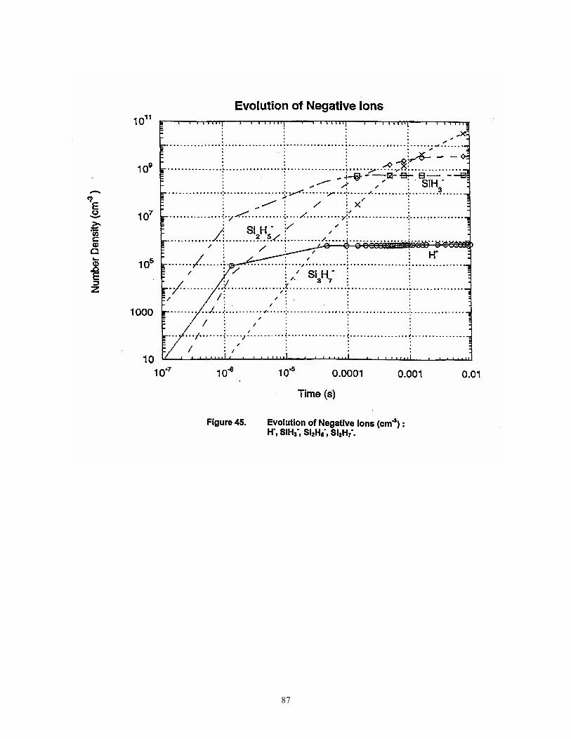
87
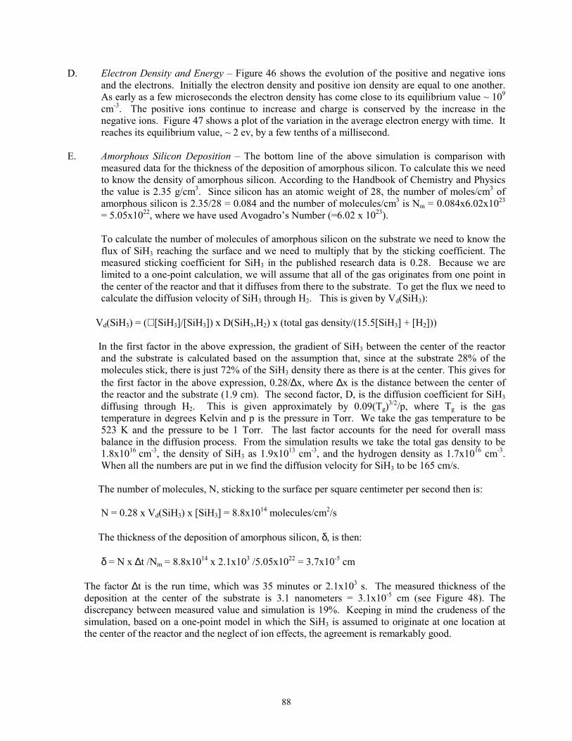
88
D. Electron Density and Energy – Figure 46 shows the evolution of the positive and negative ionsand the electrons. Initially the electron density and positive ion density are equal to one another.As early as a few microseconds the electron density has come close to its equilibrium value ~ 109
cm-3. The positive ions continue to increase and charge is conserved by the increase in thenegative ions. Figure 47 shows a plot of the variation in the average electron energy with time. Itreaches its equilibrium value, ~ 2 ev, by a few tenths of a millisecond.
E. Amorphous Silicon Deposition – The bottom line of the above simulation is comparison withmeasured data for the thickness of the deposition of amorphous silicon. To calculate this we needto know the density of amorphous silicon. According to the Handbook of Chemistry and Physicsthe value is 2.35 g/cm3. Since silicon has an atomic weight of 28, the number of moles/cm3 ofamorphous silicon is 2.35/28 = 0.084 and the number of molecules/cm3 is Nm = 0.084x6.02x1023
= 5.05x10²², where we have used Avogadro’s Number (=6.02 x 10²³).
To calculate the number of molecules of amorphous silicon on the substrate we need to know theflux of SiH3 reaching the surface and we need to multiply that by the sticking coefficient. Themeasured sticking coefficient for SiH3 in the published research data is 0.28. Because we arelimited to a one-point calculation, we will assume that all of the gas originates from one point inthe center of the reactor and that it diffuses from there to the substrate. To get the flux we need tocalculate the diffusion velocity of SiH3 through H2. This is given by Vd(SiH3):
Vd(SiH3) = (∇ [SiH3]/[SiH3]) x D(SiH3,H2) x (total gas density/(15.5[SiH3] + [H2]))
In the first factor in the above expression, the gradient of SiH3 between the center of the reactorand the substrate is calculated based on the assumption that, since at the substrate 28% of themolecules stick, there is just 72% of the SiH3 density there as there is at the center. This gives forthe first factor in the above expression, 0.28/∆x, where ∆x is the distance between the center ofthe reactor and the substrate (1.9 cm). The second factor, D, is the diffusion coefficient for SiH3diffusing through H2. This is given approximately by 0.09(Tg)3/2/p, where Tg is the gastemperature in degrees Kelvin and p is the pressure in Torr. We take the gas temperature to be523 K and the pressure to be 1 Torr. The last factor accounts for the need for overall massbalance in the diffusion process. From the simulation results we take the total gas density to be1.8x1016
cm-3, the density of SiH3 as 1.9x1013 cm-3, and the hydrogen density as 1.7x1016 cm-3.When all the numbers are put in we find the diffusion velocity for SiH3 to be 165 cm/s.
The number of molecules, N, sticking to the surface per square centimeter per second then is:
N = 0.28 x Vd(SiH3) x [SiH3] = 8.8x10¹⁴ molecules/cm2/s
The thickness of the deposition of amorphous silicon, δ, is then:
δ = N x ∆t /Nm = 8.8x1014 x 2.1x103 /5.05x1022 = 3.7x10⁻⁵ cm
The factor ∆t is the run time, which was 35 minutes or 2.1x10³ s. The measured thickness of thedeposition at the center of the substrate is 3.1 nanometers = 3.1x10⁻⁵ cm (see Figure 48). Thediscrepancy between measured value and simulation is 19%. Keeping in mind the crudeness of thesimulation, based on a one-point model in which the SiH3 is assumed to originate at one location atthe center of the reactor and the neglect of ion effects, the agreement is remarkably good.

89

90

91

REPORT DOCUMENTATION PAGE Form ApprovedOMB NO. 0704-0188
Public reporting burden for this collection of information is estimated to average 1 hour per response, including the time for reviewing instructions, searching existingdata sources, gathering and maintaining the data needed, and completing and reviewing the collection of information. Send comments regarding this burdenestimate or any other aspect of this collection of information, including suggestions for reducing this burden, to Washington Headquarters Services, Directorate forInformation Operations and Reports, 1215 Jefferson Davis Highway, Suite 1204, Arlington, VA 22202-4302, and to the Office of Management and Budget, PaperworkReduction Project (0704-0188), Washington, DC 20503.
1. AGENCY USE ONLY (Leave blank) 2. REPORT DATENovember 1999
3. REPORT TYPE AND DATES COVEREDAnnual Technical Progress Report, 22 June 1998 – 21 June 1999
4. TITLE AND SUBTITLEEfficiency and Throughput Advances in Continuous Roll-to-Roll a-Si Alloy PV ManufacturingTechnology; Annual Technical Progress Report, 22 June 1998 – 21 June 19996. AUTHOR(S)M. Izu
5. FUNDING NUMBERS
C: ZAX-8-17647-09TA: PV006101
7. PERFORMING ORGANIZATION NAME(S) AND ADDRESS(ES)Energy Conversion Devices, Inc.1675 W. Maple RoadTroy, MI 48084
8. PERFORMING ORGANIZATIONREPORT NUMBER
9. SPONSORING/MONITORING AGENCY NAME(S) AND ADDRESS(ES)National Renewable Energy Laboratory1617 Cole Blvd.Golden, CO 80401-3393
10. SPONSORING/MONITORINGAGENCY REPORT NUMBER
SR-520-27535
11. SUPPLEMENTARY NOTESNREL Technical Monitor: R.L. Mitchell
12a. DISTRIBUTION/AVAILABILITY STATEMENTNational Technical Information ServiceU.S. Department of Commerce5285 Port Royal RoadSpringfield, VA 22161
12b. DISTRIBUTION CODE
13. ABSTRACT (Maximum 200 words)This document reports on work performed by Energy Conversion Devices, Inc. (ECD) during Phase I of this subcontract. During this period,ECD researchers:1. Completed design and construction of new, improved substrate heater.2. Tested and verified improved performance of the new substrate heater in the pilot machine.3. Verified improved performance of the new substrate heater in the production machine.4. Designed and bench-tested a new infrared temperature sensor.5. Installed a prototype new infrared temperature sensor in the production machine for evaluation.6. Designed a new rolling thermocouple temperature sensor.7. Designed and bench-tested a reflectometer for the backreflector deposition machine.8. Designed and bench-tested in-line non-contacting cell diagnostic sensor; PV capacitive diagnostic system.9. Installed the in-line cell diagnostic sensor in the 5-MW a-Si deposition machine for evaluation.10. Demonstrated a new low-cost zinc metal process in the pilot backreflector machine.11. Fully tested a new cathode design for improved uniformity.
15. NUMBER OF PAGES 14. SUBJECT TERMSphotovoltaics ; Photovoltaic Manufacturing and Technology ; PVMaT ; process control ;reactive sputtering process ; substrate heaters ; temperature sensors ; reflectometers ;backreflector deposition
16. PRICE CODE
17. SECURITY CLASSIFICATIONOF REPORTUnclassified
18. SECURITYCLASSIFICATIONOF THIS PAGEUnclassified
19. SECURITY CLASSIFICATIONOF ABSTRACTUnclassified
20. LIMITATION OF ABSTRACT
UL
NSN 7540-01-280-5500 Standard Form 298 (Rev. 2-89)Prescribed by ANSI Std. Z39-18
298-102