eee-445 review: major components of a computer processor control datapath memory devices input...
TRANSCRIPT
EEE-445
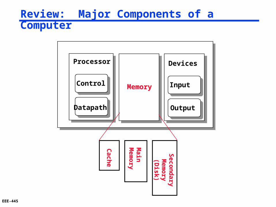
Review: Major Components of a Computer
Processor
Control
Datapath
Memory
Devices
Input
Output
Cach
e
Main
M
emo
ry
Seco
nd
ary M
emo
ry(D
isk)
EEE-445
SecondLevelCache
(SRAM)
A Typical Memory Hierarchy
Control
Datapath
SecondaryMemory(Disk)
On-Chip Components
RegF
ile
MainMemory(DRAM)
Data
Cache
InstrC
ache
ITLB
DT
LB
Speed (ns): .1’s 1’s 10’s 100’s 1,000’s
Size (bytes): 100’s K’s 10K’s M’s T’s
Cost: highest lowest
By taking advantage of the principle of locality: Present the user with as much memory as is available in the
cheapest technology. Provide access at the speed offered by the fastest technology.
EEE-445
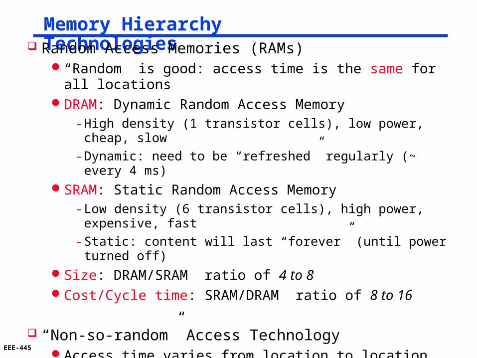
Memory Hierarchy Technologies Random Access Memories (RAMs)
“Random” is good: access time is the same for all locations DRAM: Dynamic Random Access Memory
- High density (1 transistor cells), low power, cheap, slow
- Dynamic: need to be “refreshed” regularly (~ every 4 ms) SRAM: Static Random Access Memory
- Low density (6 transistor cells), high power, expensive, fast
- Static: content will last “forever” (until power turned off) Size: DRAM/SRAM ratio of 4 to 8 Cost/Cycle time: SRAM/DRAM ratio of 8 to 16
“Non-so-random” Access Technology Access time varies from location to location and from time to
time (e.g., disk, CDROM)
EEE-445
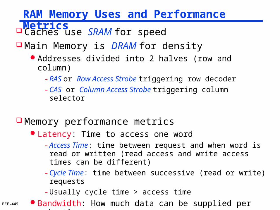
RAM Memory Uses and Performance Metrics
Caches use SRAM for speed Main Memory is DRAM for density
Addresses divided into 2 halves (row and column)- RAS or Row Access Strobe triggering row decoder
- CAS or Column Access Strobe triggering column selector
Memory performance metrics Latency: Time to access one word
- Access Time: time between request and when word is read or written (read access and write access times can be different)
- Cycle Time: time between successive (read or write) requests
- Usually cycle time > access time Bandwidth: How much data can be supplied per unit time
- width of the data channel * the rate at which it can be used
EEE-445
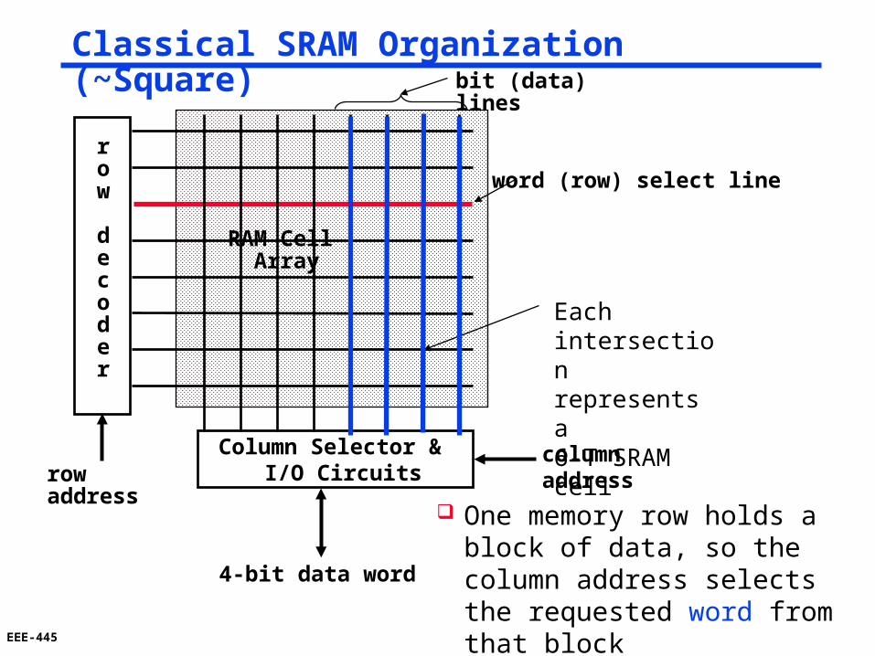
Classical SRAM Organization (~Square)
row
decoder
rowaddress
4-bit data word
RAM Cell Array
word (row) select line
bit (data) lines
Each intersection represents a 6-T SRAM cell
Column Selector & I/O Circuits
columnaddress
One memory row holds a block of data, so the column address selects the requested word from that block
EEE-445
data bitdata bit
Classical DRAM Organization (~Square Planes)
row
decoder
rowaddress
Column Selector & I/O Circuits
columnaddress
data bit
bit (data) lines
Each intersection represents a 1-T DRAM cell
The column address selects the requested bit from the row in each planedata word
. . .
. . .
RAM Cell Array
word (row) select line
n planes (where n is the # of bits in the word)
EEE-445
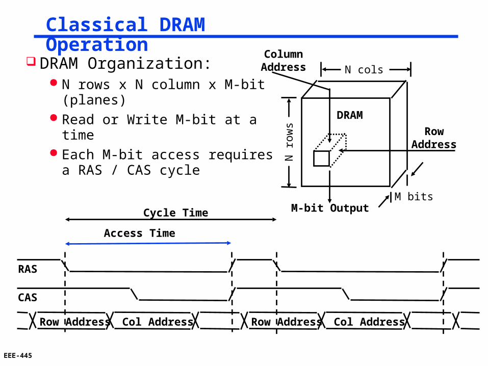
Classical DRAM Operation
DRAM Organization: N rows x N column x M-bit
(planes) Read or Write M-bit at a time Each M-bit access requires
a RAS / CAS cycle
Row Address
CAS
RAS
Col Address Row Address Col Address
Access Time
N r
ows
N cols
DRAM
M bits
RowAddress
ColumnAddress
M-bit OutputCycle Time
EEE-445
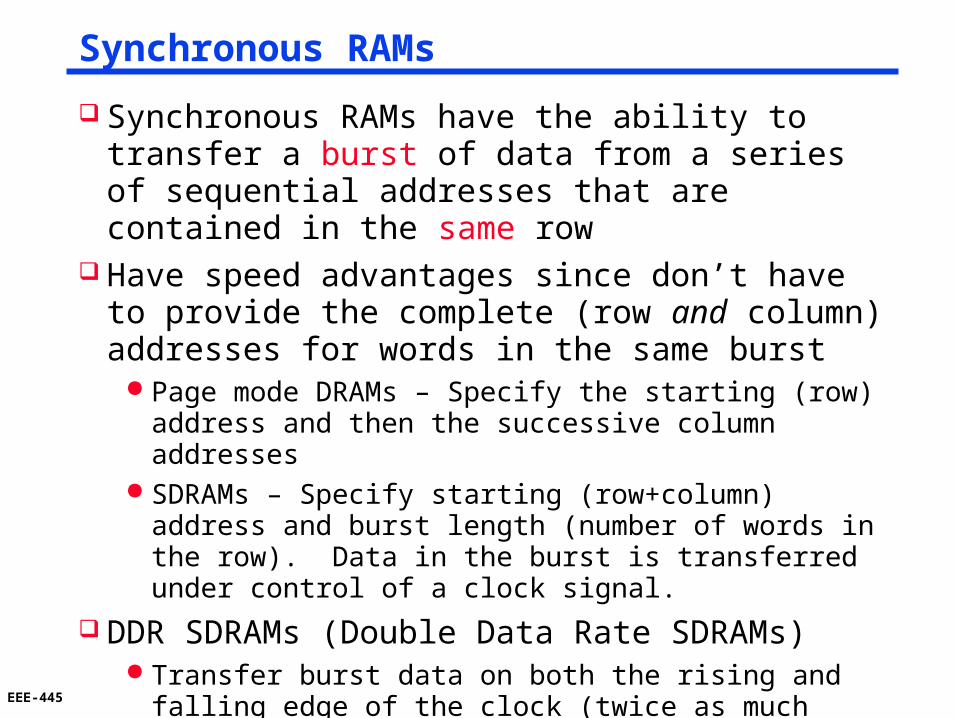
Synchronous RAMs
Synchronous RAMs have the ability to transfer a burst of data from a series of sequential addresses that are contained in the same row
Have speed advantages since don’t have to provide the complete (row and column) addresses for words in the same burst
Page mode DRAMs – Specify the starting (row) address and then the successive column addresses
SDRAMs – Specify starting (row+column) address and burst length (number of words in the row). Data in the burst is transferred under control of a clock signal.
DDR SDRAMs (Double Data Rate SDRAMs) Transfer burst data on both the rising and falling edge of
the clock (twice as much bandwidth)
EEE-445
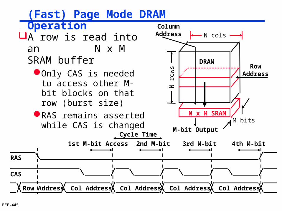
N r
ows
N cols
DRAM
ColumnAddress
M-bit Output
M bits N x M SRAM
RowAddress
(Fast) Page Mode DRAM Operation
Row Address
CAS
RAS
Col Address Col Address
1st M-bit Access
Col Address Col Address
2nd M-bit 3rd M-bit 4th M-bit
A row is read into an N x M SRAM buffer
Only CAS is needed to access other M-bit blocks on that row (burst size)
RAS remains asserted while CAS is changed
Cycle Time
EEE-445
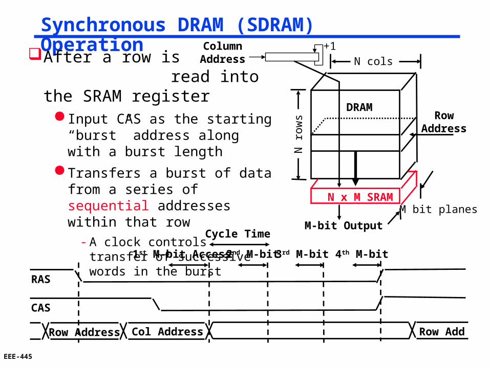
N r
ows
N cols
DRAM
ColumnAddress
M-bit Output
M bit planes N x M SRAM
RowAddress
Synchronous DRAM (SDRAM) OperationAfter a row is read into the SRAM register
Input CAS as the starting “burst” address along with a burst length
Transfers a burst of data from a series of sequential addresses within that row
- A clock controls transfer of successive words in the burst
+1
Row Address
CAS
RAS
Col Address
1st M-bit Access 2nd M-bit 3rd M-bit 4th M-bit
Cycle Time
Row Add
EEE-445
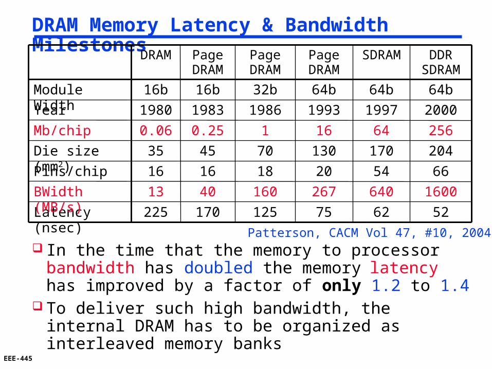
DRAM Memory Latency & Bandwidth Milestones
In the time that the memory to processor bandwidth has doubled the memory latency has improved by a factor of only 1.2 to 1.4
To deliver such high bandwidth, the internal DRAM has to be organized as interleaved memory banks
526275125170225Latency (nsec)
16006402671604013BWidth (MB/s)
665420181616Pins/chip
204170130704535Die size (mm2)
256641610.250.06Mb/chip
200019971993198619831980Year
64b64b64b32b16b16bModule Width
DDR SDRAM
SDRAMPage DRAM
Page DRAM
Page DRAM
DRAM
Patterson, CACM Vol 47, #10, 2004
EEE-445
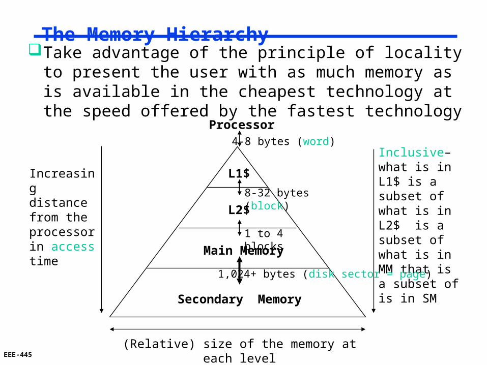
The Memory Hierarchy
L1$
L2$
Main Memory
Secondary Memory
Increasing distance from the processor in access time
Processor
(Relative) size of the memory at each level
Inclusive– what is in L1$ is a subset of what is in L2$ is a subset of what is in MM that is a subset of is in SM
4-8 bytes (word)
1 to 4 blocks
1,024+ bytes (disk sector = page)
8-32 bytes (block)
Take advantage of the principle of locality to present the user with as much memory as is available in the cheapest technology at the speed offered by the fastest technology
EEE-445
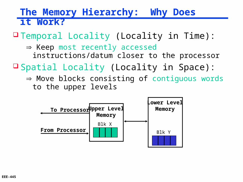
The Memory Hierarchy: Why Does it Work?
Temporal Locality (Locality in Time): Keep most recently accessed instructions/datum closer to
the processor
Spatial Locality (Locality in Space): Move blocks consisting of contiguous words to the upper
levels
Lower LevelMemoryUpper Level
MemoryTo Processor
From ProcessorBlk X
Blk Y
EEE-445
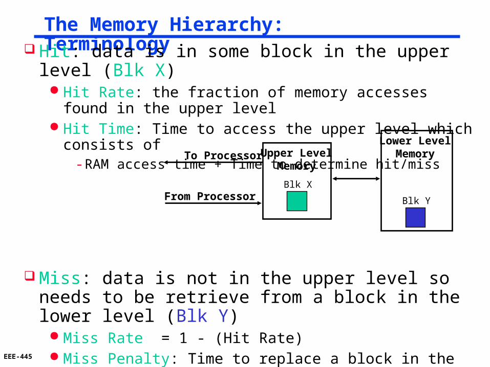
The Memory Hierarchy: Terminology Hit: data is in some block in the upper level (Blk X) Hit Rate: the fraction of memory accesses found in the upper
level Hit Time: Time to access the upper level which consists of
- RAM access time + Time to determine hit/miss
Miss: data is not in the upper level so needs to be retrieve from a block in the lower level (Blk Y)
Miss Rate = 1 - (Hit Rate) Miss Penalty: Time to replace a block in the upper level
+ Time to deliver the block the processor Hit Time << Miss Penalty
Lower LevelMemoryUpper Level
MemoryTo Processor
From ProcessorBlk X
Blk Y
EEE-445
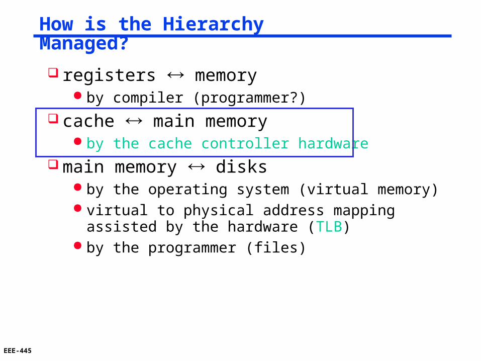
How is the Hierarchy Managed?
registers memory by compiler (programmer?)
cache main memory by the cache controller hardware
main memory disks by the operating system (virtual memory) virtual to physical address mapping assisted by the
hardware (TLB) by the programmer (files)
EEE-445
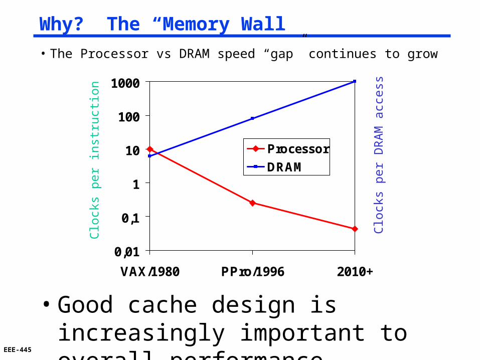
Why? The “Memory Wall”
• The Processor vs DRAM speed “gap” continues to grow
0,01
0,1
1
10
100
1000
VAX/1980 PPro/1996 2010+
Processor
DRAM
Clo
cks
per
inst
ruct
ion
Clo
cks
per
DR
AM
acc
ess
• Good cache design is increasingly important to overall performance
EEE-445
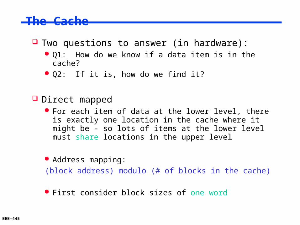
Two questions to answer (in hardware): Q1: How do we know if a data item is in the cache? Q2: If it is, how do we find it?
Direct mapped For each item of data at the lower level, there is exactly
one location in the cache where it might be - so lots of items at the lower level must share locations in the upper level
Address mapping:
(block address) modulo (# of blocks in the cache)
First consider block sizes of one word
The Cache
EEE-445
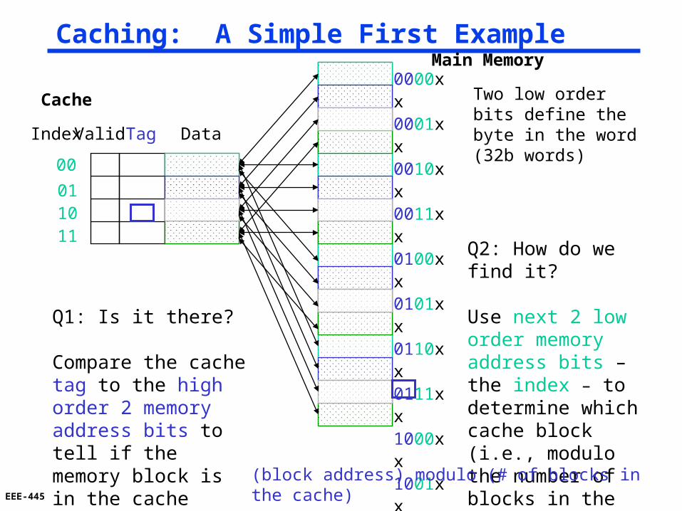
Caching: A Simple First Example
00
011011
Cache
Main Memory
Q2: How do we find it?
Use next 2 low order memory address bits – the index – to determine which cache block (i.e., modulo the number of blocks in the cache)
Tag Data
Q1: Is it there?
Compare the cache tag to the high order 2 memory address bits to tell if the memory block is in the cache
Valid
0000xx0001xx0010xx0011xx0100xx0101xx0110xx0111xx1000xx1001xx1010xx1011xx1100xx1101xx1110xx1111xx
Two low order bits define the byte in the word (32b words)
(block address) modulo (# of blocks in the cache)
Index
EEE-445
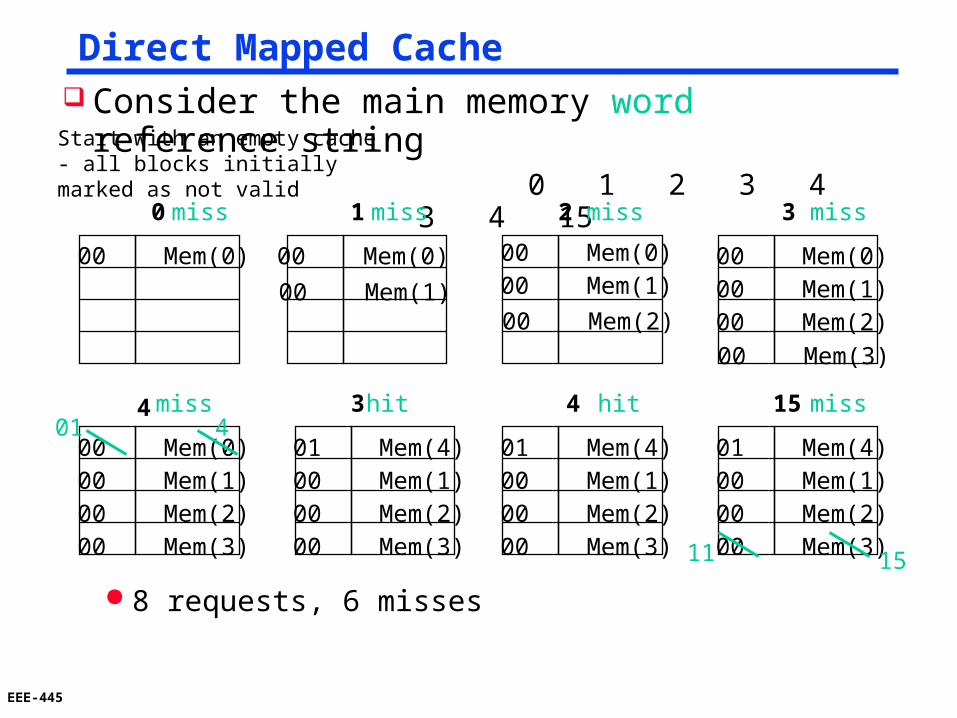
Direct Mapped Cache
0 1 2 3
4 3 4 15
Consider the main memory word reference string 0 1 2 3 4 3 4 15
00 Mem(0) 00 Mem(0)00 Mem(1)
00 Mem(0) 00 Mem(0)00 Mem(1)00 Mem(2)
miss miss miss miss
miss misshit hit
00 Mem(0)00 Mem(1)00 Mem(2)00 Mem(3)
01 Mem(4)00 Mem(1)00 Mem(2)00 Mem(3)
01 Mem(4)00 Mem(1)00 Mem(2)00 Mem(3)
01 Mem(4)00 Mem(1)00 Mem(2)00 Mem(3)
01 4
11 15
00 Mem(1)00 Mem(2)
00 Mem(3)
Start with an empty cache - all blocks initially marked as not valid
8 requests, 6 misses
EEE-445
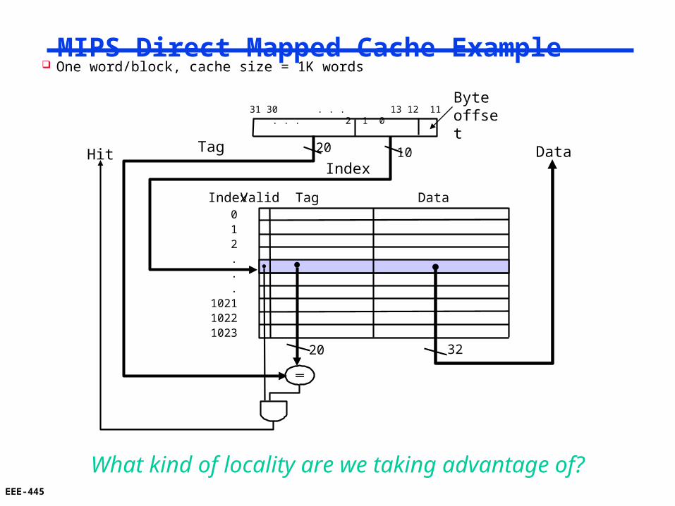
One word/block, cache size = 1K wordsMIPS Direct Mapped Cache Example
20Tag 10Index
Data Index TagValid012...
102110221023
31 30 . . . 13 12 11 . . . 2 1 0Byte offset
What kind of locality are we taking advantage of?
20
Data
32
Hit