ece 331 – digital system designece.gmu.edu/~clorie/spring11/ece-331/lectures/lecture_16.pdf ·...
TRANSCRIPT
ECE 331 – Digital System Design
Multiplexers, Decoders and Encoders
(Lecture #16)
The slides included herein were taken from the materials accompanying
Fundamentals of Logic Design, 6th Edition, by Roth and Kinney,
and were used with permission from Cengage Learning.
Spring 2011 ECE 331 - Digital System Design 2
Multiplexers
Spring 2011 ECE 331 - Digital System Design 3
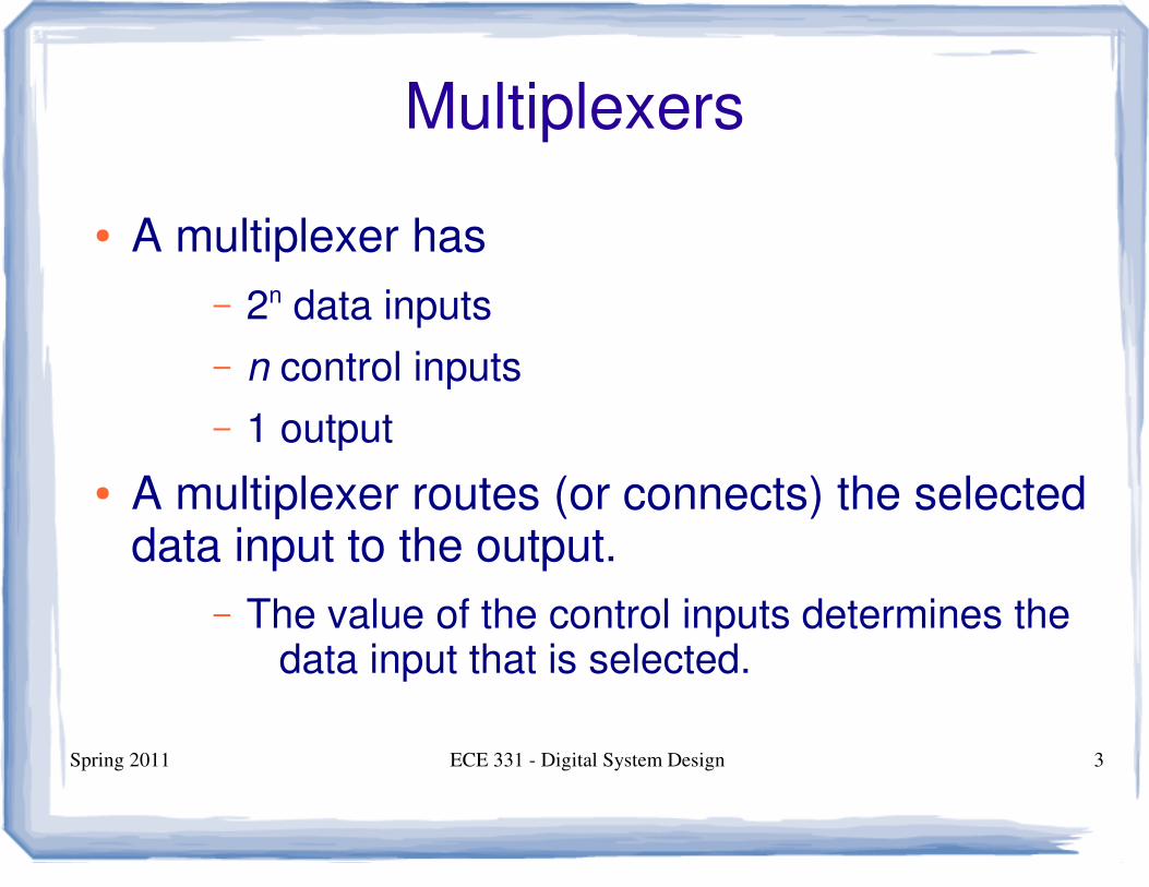
Multiplexers
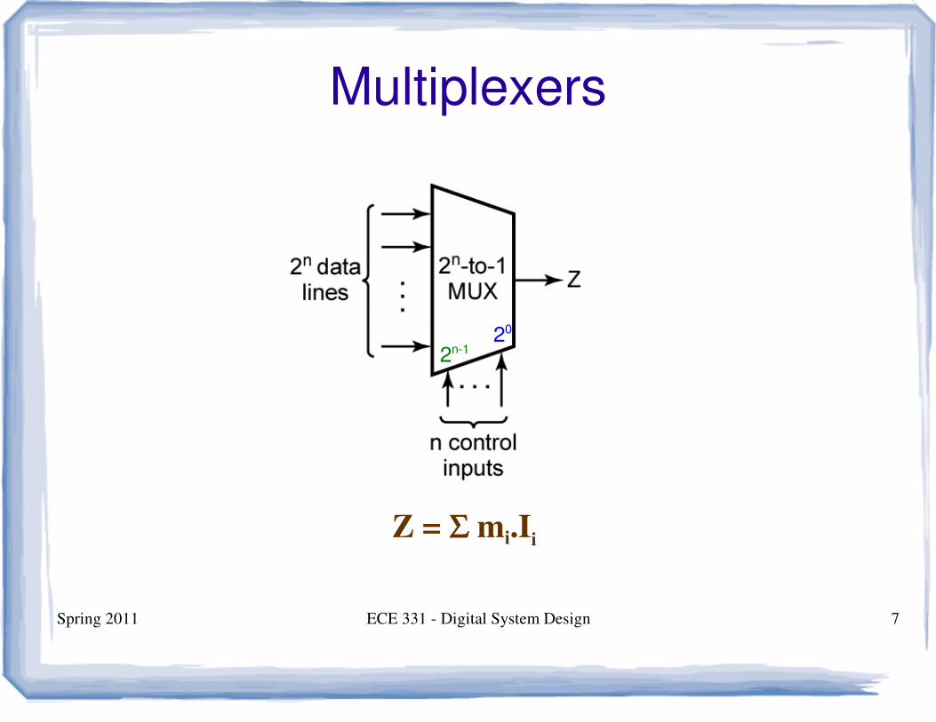
● A multiplexer has
– 2n data inputs
– n control inputs
– 1 output
● A multiplexer routes (or connects) the selected data input to the output.
– The value of the control inputs determines the data input that is selected.
Spring 2011 ECE 331 - Digital System Design 4
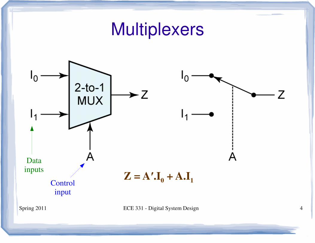
Multiplexers
Z = A′.I0 + A.I
1
Datainputs
Controlinput
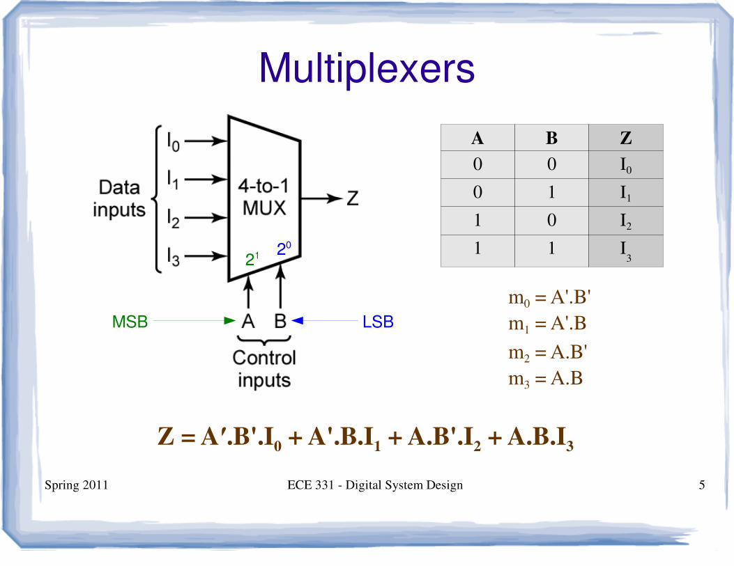
Spring 2011 ECE 331 - Digital System Design 5
Multiplexers
Z = A′.B'.I0 + A'.B.I
1 + A.B'.I
2 + A.B.I
3
MSB LSB
A B Z
0 0 I0
0 1 I1
1 0 I2
1 1 I321 20
m0 = A'.B'
m1 = A'.B
m2 = A.B'
m3 = A.B
Spring 2011 ECE 331 - Digital System Design 6
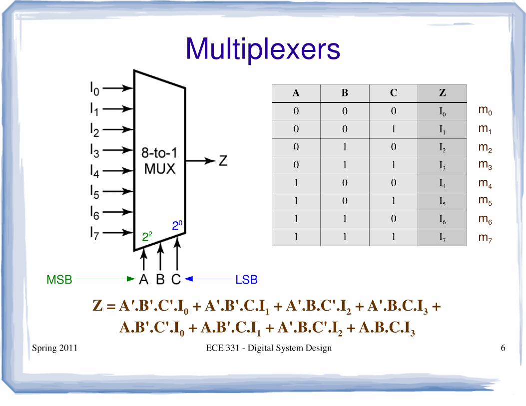
Multiplexers
Z = A′.B'.C'.I0 + A'.B'.C.I
1 + A'.B.C'.I
2 + A'.B.C.I
3 +
A.B'.C'.I0 + A.B'.C.I
1 + A'.B.C'.I
2 + A.B.C.I
3
MSB LSB
A B C Z
0 0 0 I0
0 0 1 I1
0 1 0 I2
0 1 1 I3
1 0 0 I4
1 0 1 I5
1 1 0 I6
1 1 1 I72220
m0
m1
m2
m3
m4
m5
m6
m7
Spring 2011 ECE 331 - Digital System Design 7
Multiplexers
2n-120
Z = ΣΣΣΣ mi.Ii
Spring 2011 ECE 331 - Digital System Design 8
Multiplexers in VHDL
Spring 2011 ECE 331 - Digital System Design 9
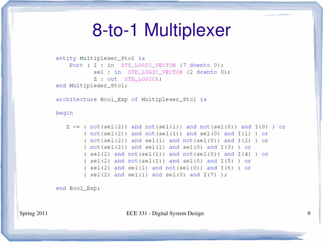
8-to-1 Multiplexer
Spring 2011 ECE 331 - Digital System Design 10
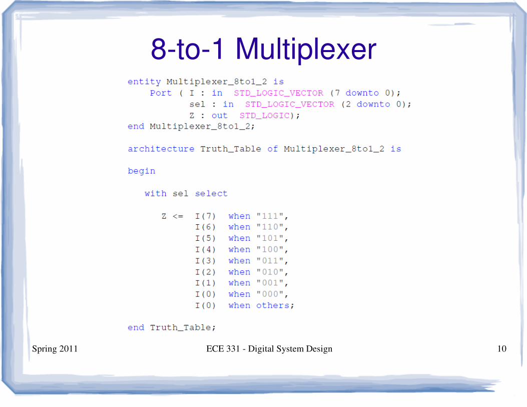
8-to-1 Multiplexer

Spring 2011 ECE 331 - Digital System Design 11
Decoders
Spring 2011 ECE 331 - Digital System Design 12
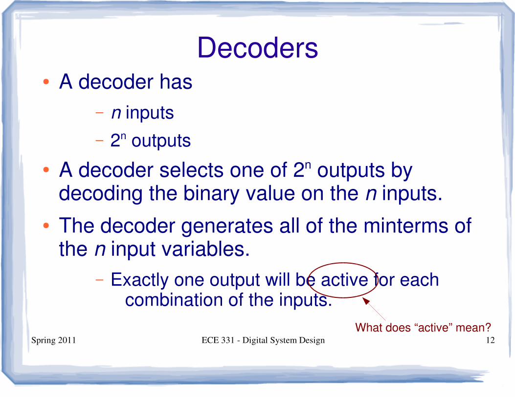
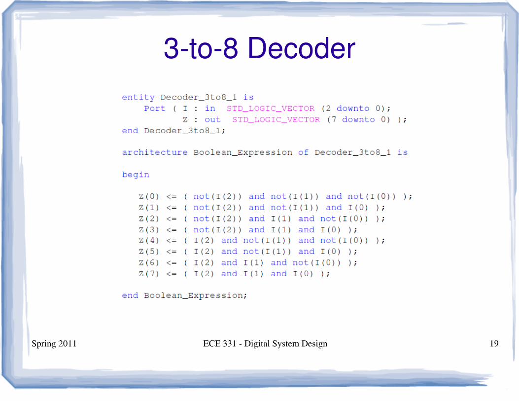
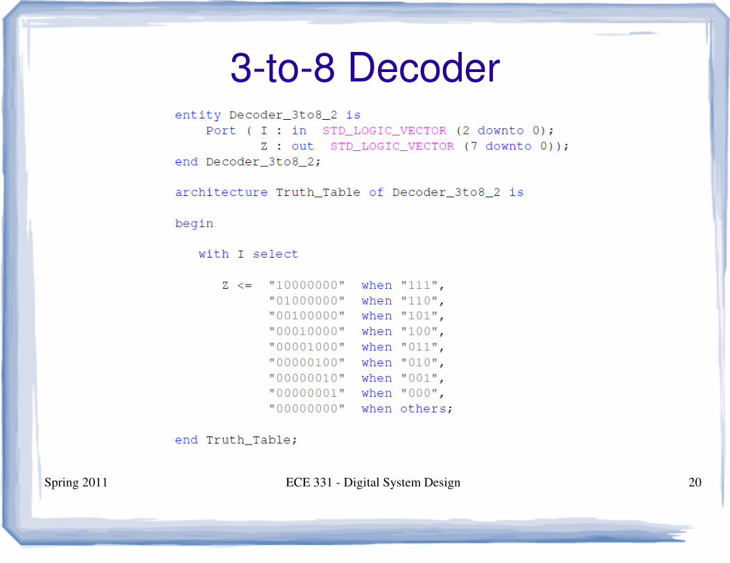
Decoders● A decoder has
– n inputs
– 2n outputs
● A decoder selects one of 2n outputs by decoding the binary value on the n inputs.
● The decoder generates all of the minterms of the n input variables.
– Exactly one output will be active for each combination of the inputs.
What does “active” mean?
Spring 2011 ECE 331 - Digital System Design 13
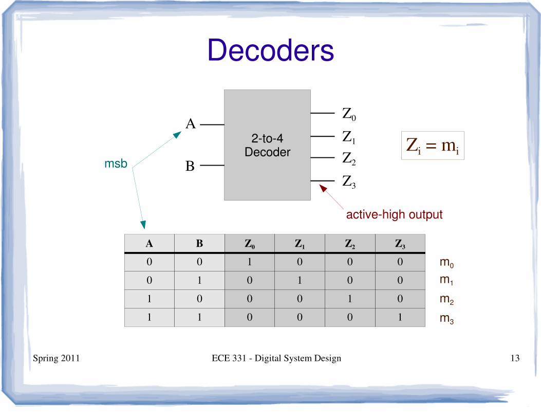
Decoders
A B Z0 Z1 Z2 Z3
0 0 1 0 0 0
0 1 0 1 0 0
1 0 0 0 1 0
1 1 0 0 0 1
msb
2-to-4Decoder
A
B
Z0
Z1
Z2
Z3
active-high output
Zi = mi
m0
m1
m2
m3
Spring 2011 ECE 331 - Digital System Design 14
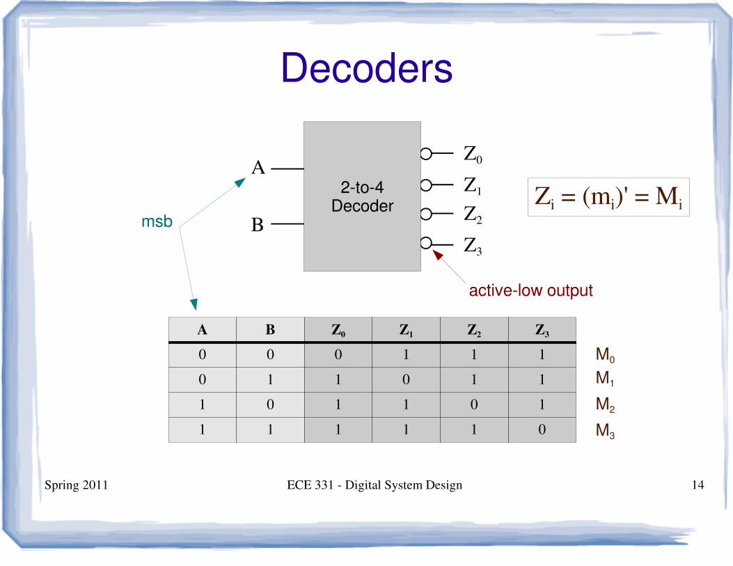
Decoders
A B Z0 Z1 Z2 Z3
0 0 0 1 1 1
0 1 1 0 1 1
1 0 1 1 0 1
1 1 1 1 1 0
msb
active-low output
Zi = (mi)' = Mi
M0
M1
M2
M3
A
B
Z0
Z1
Z2
Z3
2-to-4Decoder
Spring 2011 ECE 331 - Digital System Design 15
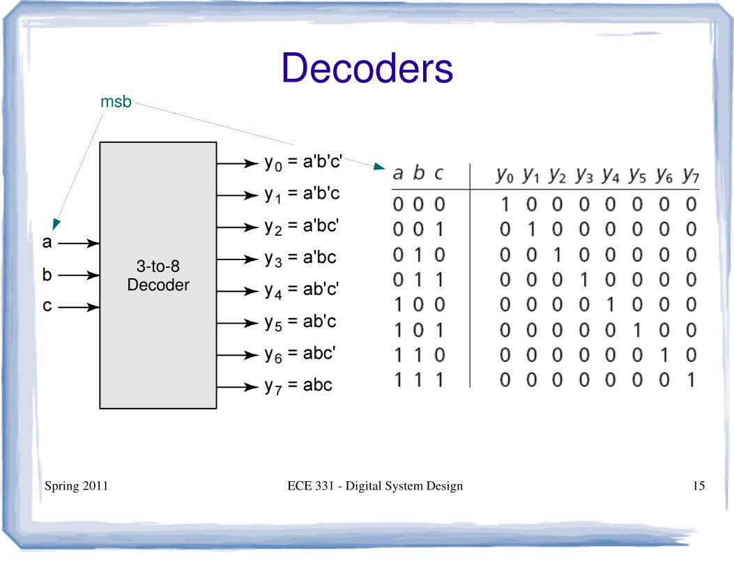
Decodersmsb
3-to-8Decoder
Spring 2011 ECE 331 - Digital System Design 16
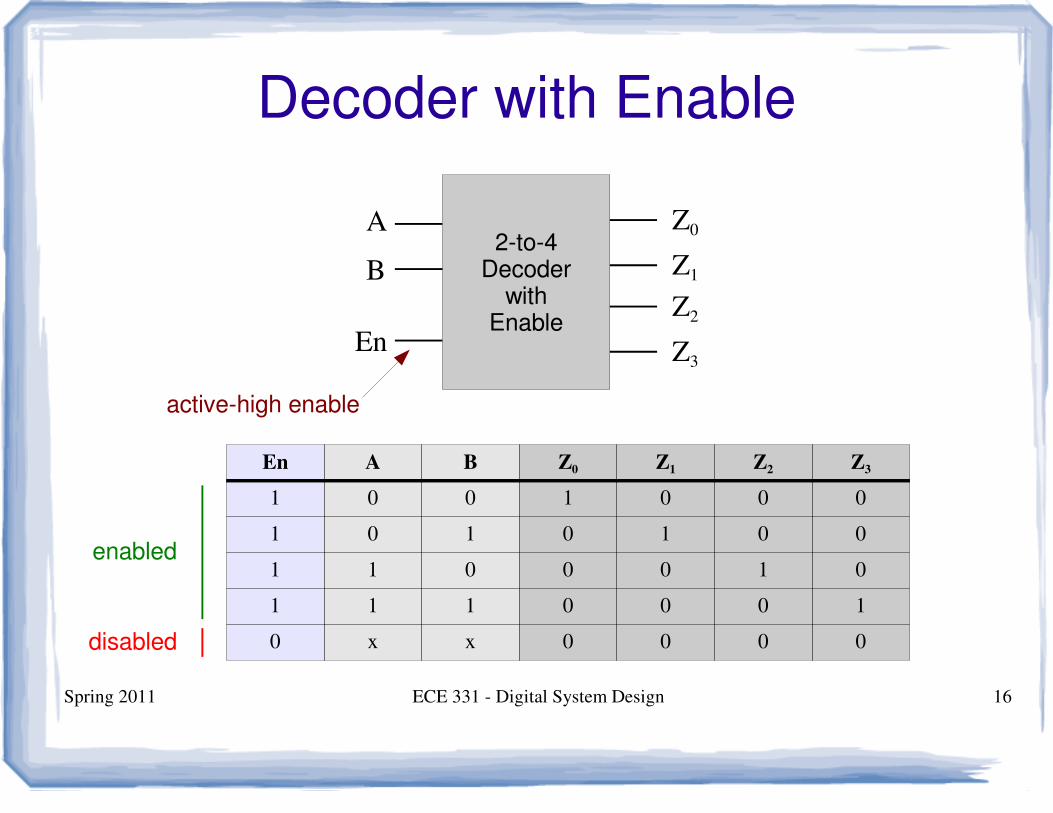
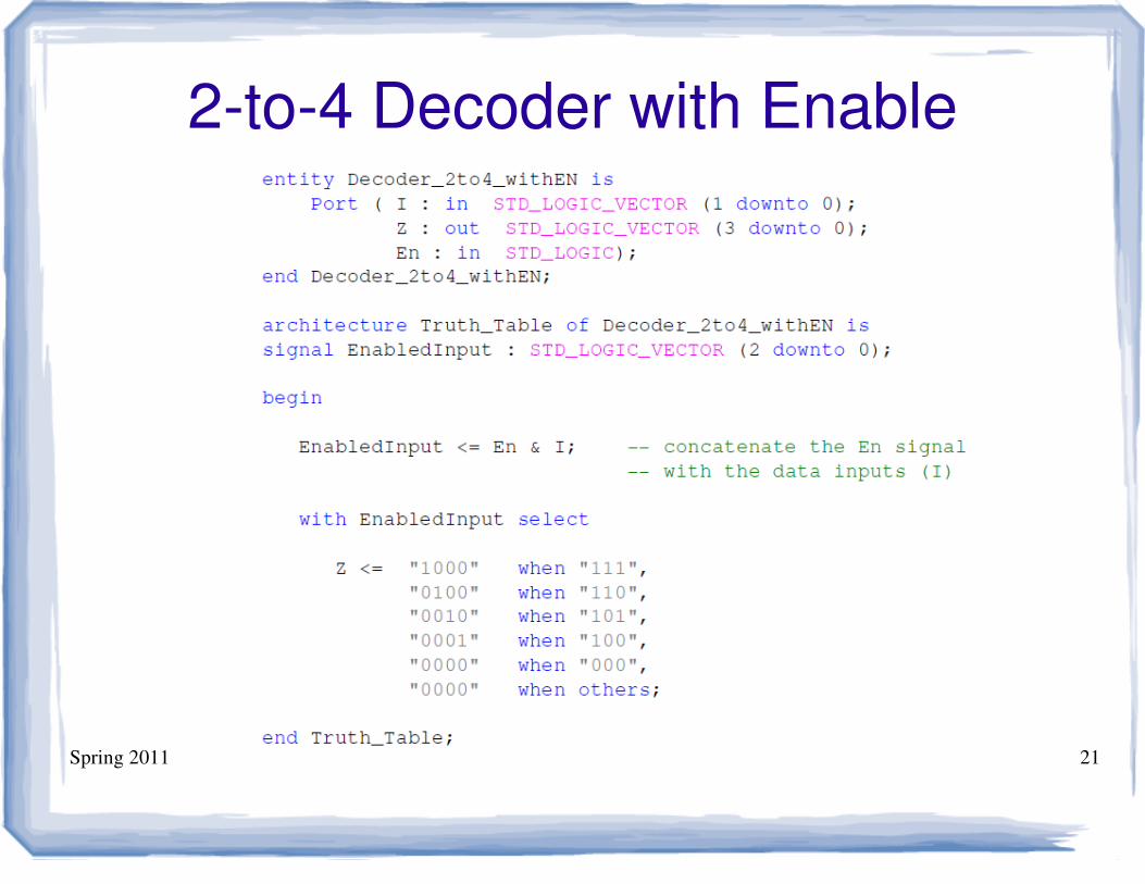
Decoder with Enable
En A B Z0 Z1 Z2 Z3
1 0 0 1 0 0 0
1 0 1 0 1 0 0
1 1 0 0 0 1 0
1 1 1 0 0 0 1
0 x x 0 0 0 0
enabled
disabled
active-high enable
En
2-to-4Decoder
withEnable
A Z0
Z1
Z2
Z3
B
Spring 2011 ECE 331 - Digital System Design 17
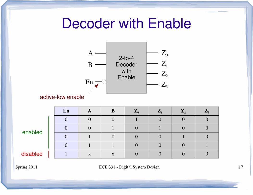
Decoder with Enable
En A B Z0 Z1 Z2 Z3
0 0 0 1 0 0 0
0 0 1 0 1 0 0
0 1 0 0 0 1 0
0 1 1 0 0 0 1
1 x x 0 0 0 0
enabled
disabled
active-low enable
En
2-to-4Decoder
withEnable
A Z0
Z1
Z2
Z3
B
Spring 2011 ECE 331 - Digital System Design 18
Decoders in VHDL
Spring 2011 ECE 331 - Digital System Design 19
3-to-8 Decoder
Spring 2011 ECE 331 - Digital System Design 20
3-to-8 Decoder
Spring 2011 ECE 331 - Digital System Design 21
2-to-4 Decoder with Enable
Spring 2011 ECE 331 - Digital System Design 22
Encoders
Spring 2011 ECE 331 - Digital System Design 23
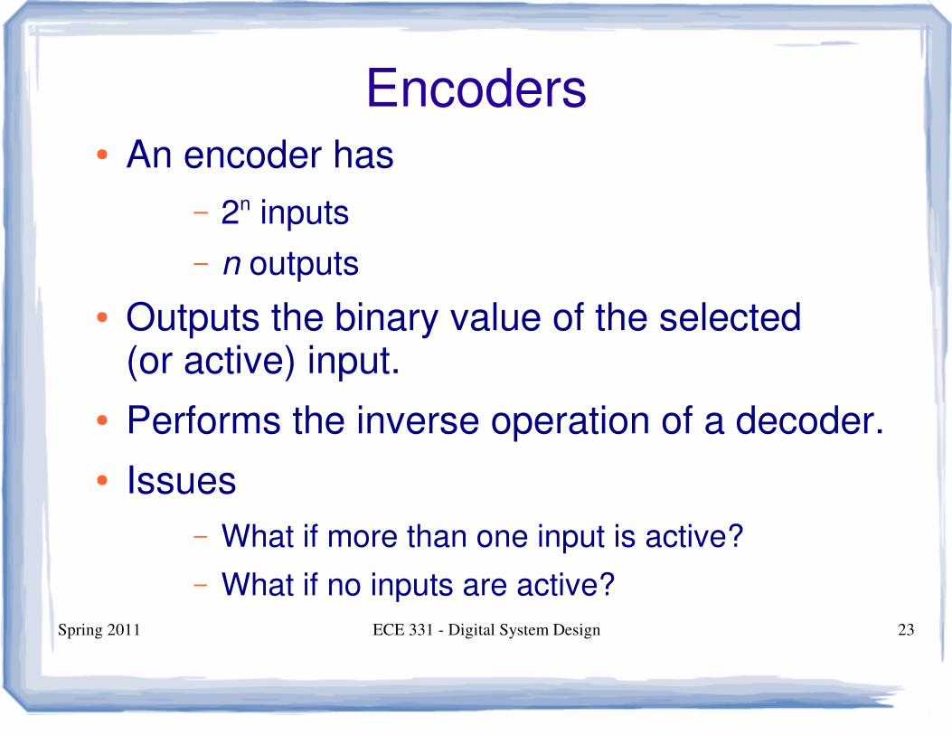
Encoders● An encoder has
– 2n inputs
– n outputs
● Outputs the binary value of the selected (or active) input.
● Performs the inverse operation of a decoder.
● Issues
– What if more than one input is active?
– What if no inputs are active?
Spring 2011 ECE 331 - Digital System Design 24
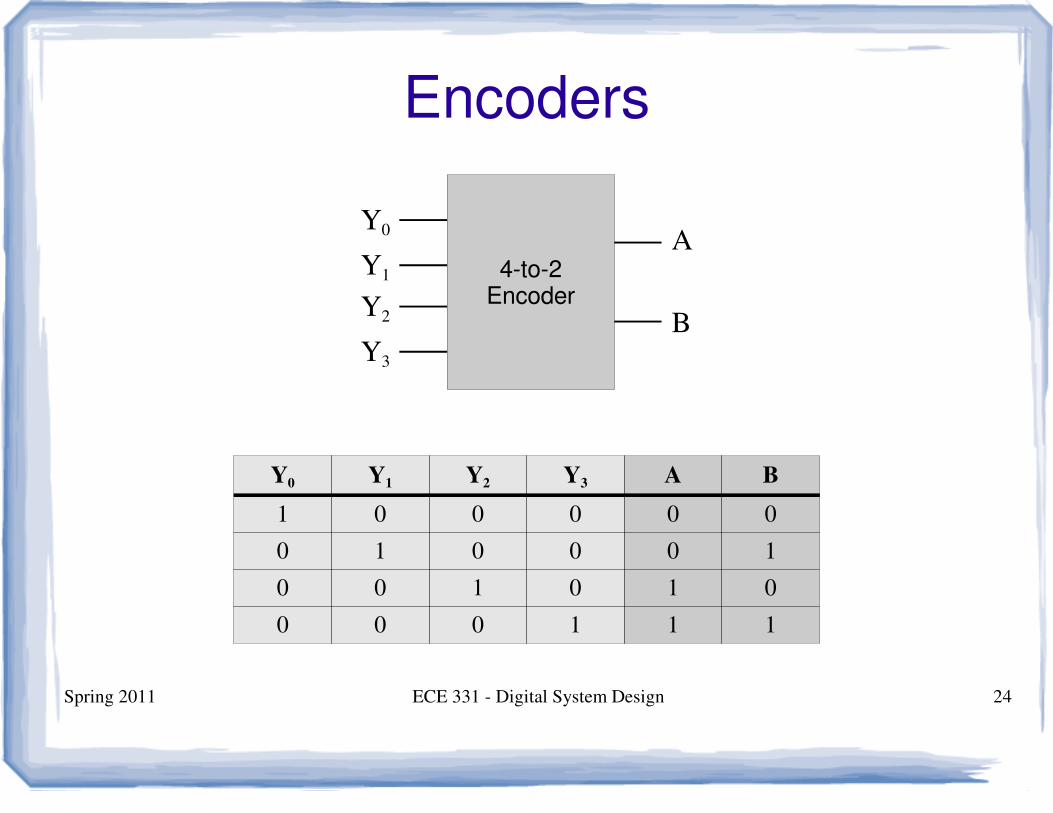
Encoders
Y0 Y1 Y2 Y3 A B
1 0 0 0 0 0
0 1 0 0 0 1
0 0 1 0 1 0
0 0 0 1 1 1
4-to-2Encoder
A
B
Y0
Y1
Y2
Y3
Spring 2011 ECE 331 - Digital System Design 25
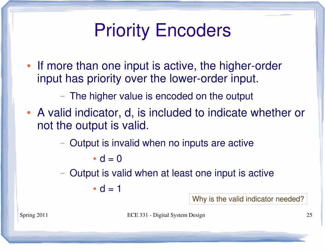
Priority Encoders
● If more than one input is active, the higher-order input has priority over the lower-order input.
– The higher value is encoded on the output
● A valid indicator, d, is included to indicate whether or not the output is valid.
– Output is invalid when no inputs are active
● d = 0
– Output is valid when at least one input is active
● d = 1Why is the valid indicator needed?
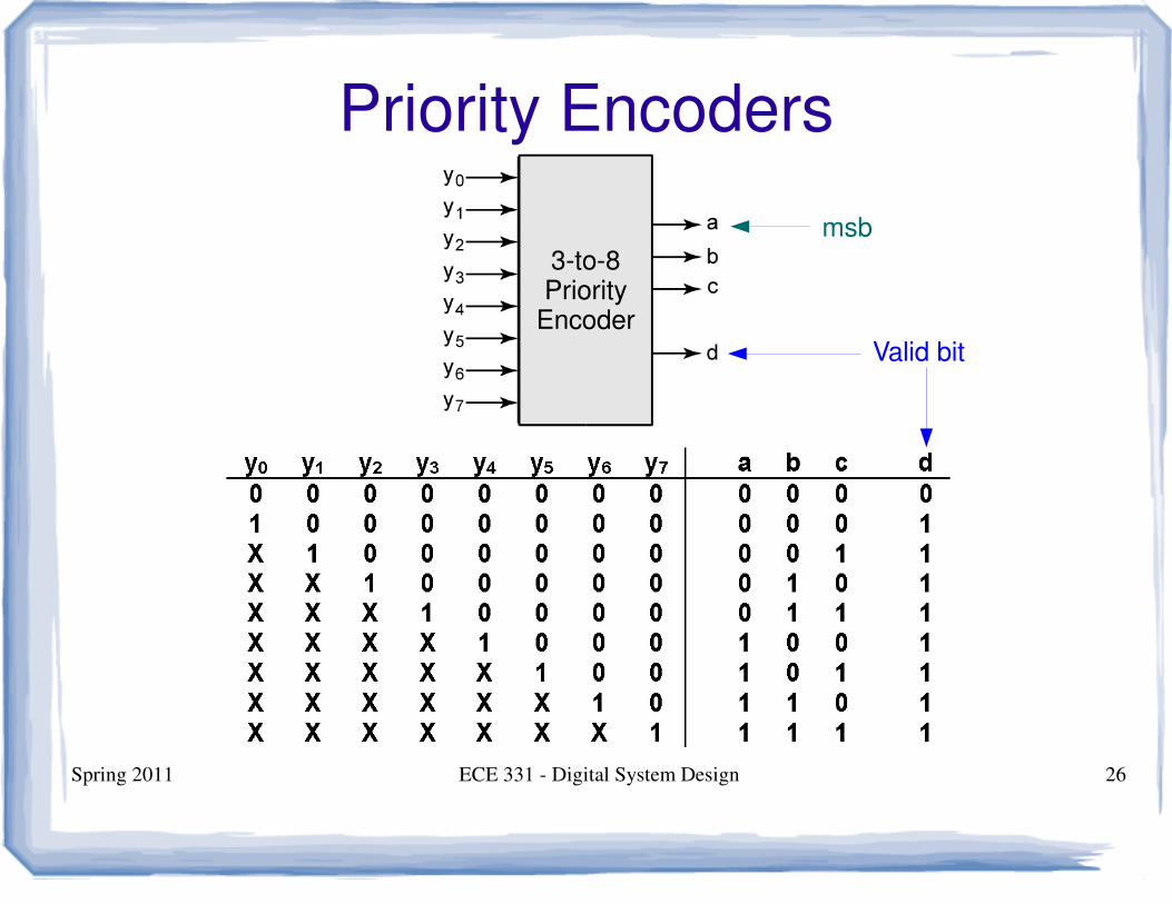
Spring 2011 ECE 331 - Digital System Design 26
Priority Encoders
Valid bit
msb
3-to-8Priority
Encoder
Spring 2011 ECE 331 - Digital System Design 27
Encoders in VHDL
Spring 2011 ECE 331 - Digital System Design 28
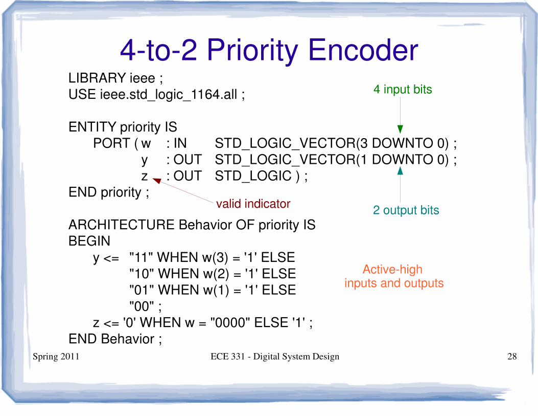
LIBRARY ieee ;
USE ieee.std_logic_1164.all ;
ENTITY priority IS
PORT ( w : IN STD_LOGIC_VECTOR(3 DOWNTO 0) ;
y : OUT STD_LOGIC_VECTOR(1 DOWNTO 0) ;
z : OUT STD_LOGIC ) ;
END priority ;
ARCHITECTURE Behavior OF priority IS
BEGIN
y <= "11" WHEN w(3) = '1' ELSE
"10" WHEN w(2) = '1' ELSE
"01" WHEN w(1) = '1' ELSE
"00" ;
z <= '0' WHEN w = "0000" ELSE '1' ;
END Behavior ;
4-to-2 Priority Encoder4 input bits
2 output bitsvalid indicator
Active-high inputs and outputs
Spring 2011 ECE 331 - Digital System Design 29
Circuit Design using Multiplexers
Spring 2011 ECE 331 - Digital System Design 30
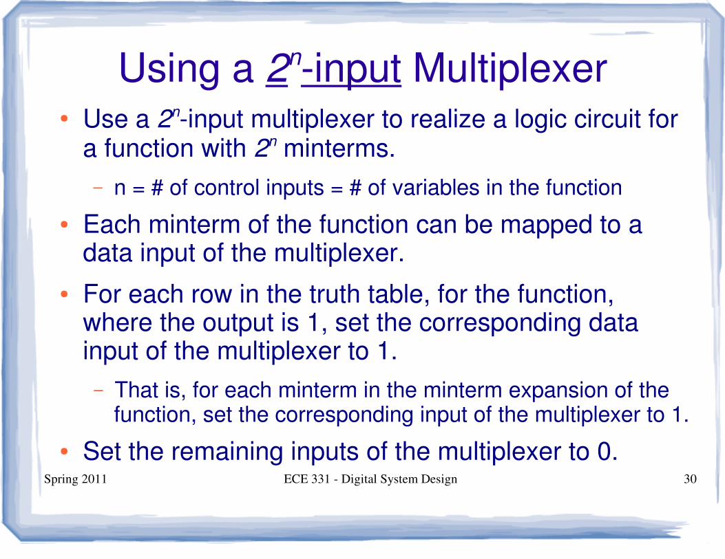
Using a 2n-input Multiplexer● Use a 2n-input multiplexer to realize a logic circuit for
a function with 2n minterms.
– n = # of control inputs = # of variables in the function
● Each minterm of the function can be mapped to a data input of the multiplexer.
● For each row in the truth table, for the function, where the output is 1, set the corresponding data input of the multiplexer to 1.
– That is, for each minterm in the minterm expansion of the function, set the corresponding input of the multiplexer to 1.
● Set the remaining inputs of the multiplexer to 0.
Spring 2011 ECE 331 - Digital System Design 31
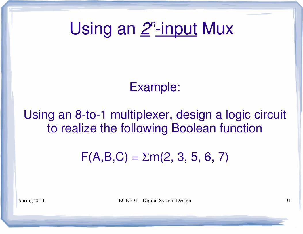
Using an 2n-input Mux
Example:
Using an 8-to-1 multiplexer, design a logic circuit to realize the following Boolean function
F(A,B,C) = Σm(2, 3, 5, 6, 7)
Spring 2011 ECE 331 - Digital System Design 32
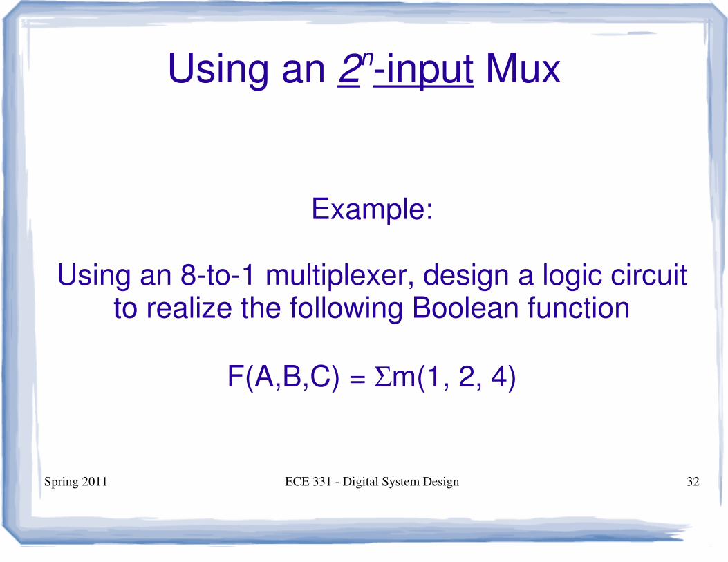
Using an 2n-input Mux
Example:
Using an 8-to-1 multiplexer, design a logic circuit to realize the following Boolean function
F(A,B,C) = Σm(1, 2, 4)
Spring 2011 33
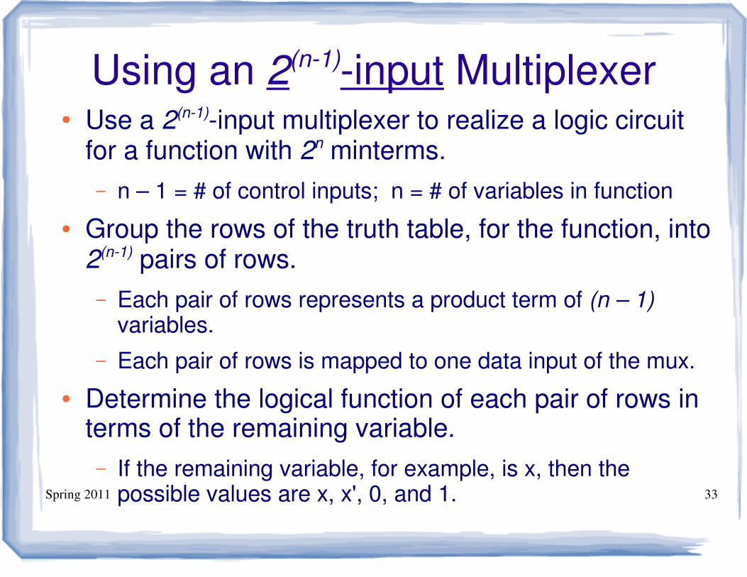
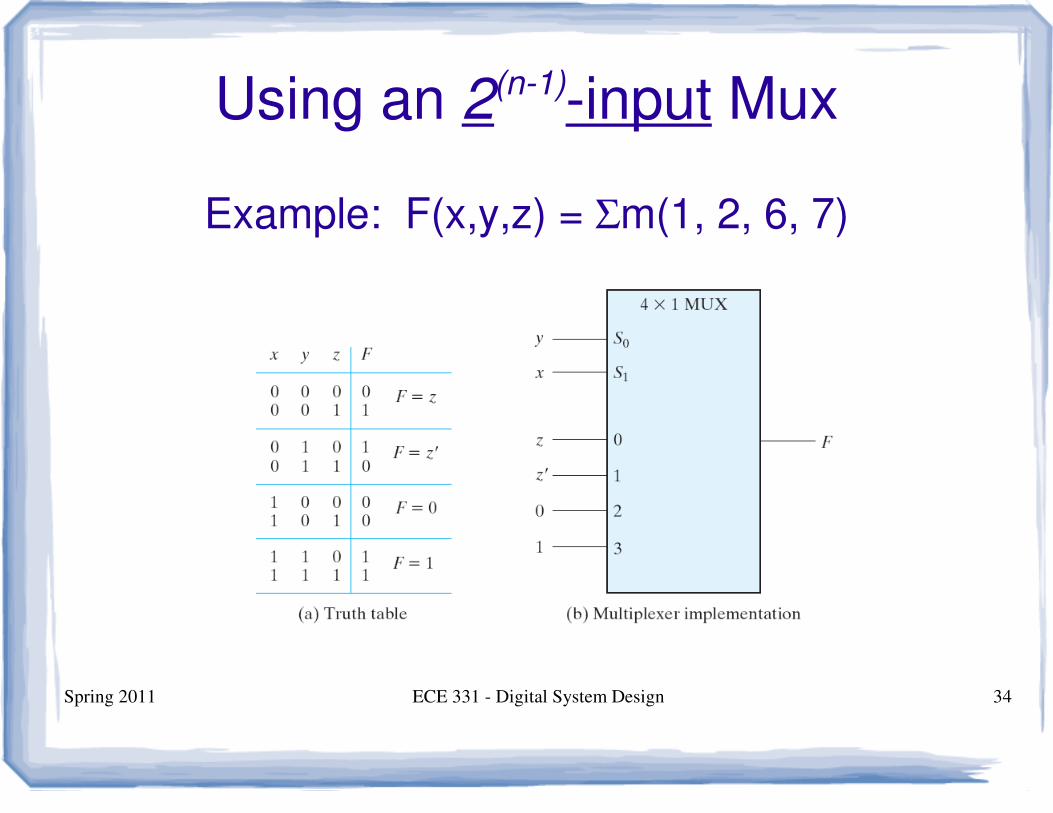
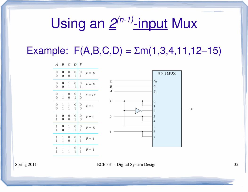
Using an 2(n-1)-input Multiplexer● Use a 2(n-1)-input multiplexer to realize a logic circuit
for a function with 2n minterms.
– n – 1 = # of control inputs; n = # of variables in function
● Group the rows of the truth table, for the function, into 2(n-1) pairs of rows.
– Each pair of rows represents a product term of (n – 1) variables.
– Each pair of rows is mapped to one data input of the mux.
● Determine the logical function of each pair of rows in terms of the remaining variable.
– If the remaining variable, for example, is x, then the possible values are x, x', 0, and 1.
Spring 2011 ECE 331 - Digital System Design 34
Using an 2(n-1)-input Mux
Example: F(x,y,z) = Σm(1, 2, 6, 7)
Spring 2011 ECE 331 - Digital System Design 35
Using an 2(n-1)-input Mux
Example: F(A,B,C,D) = Σm(1,3,4,11,12–15)
Spring 2011 ECE 331 - Digital System Design 36
Using a 2(n-2)-input Mux
A similar design approach can be implemented using a 2(n-2)-input multiplexer.
Spring 2011 ECE 331 - Digital System Design 37
Circuit Design using Decoders
Spring 2011 ECE 331 - Digital System Design 38
Using an n-output Decoder
● Use an n-output decoder to realize a logic circuit for a function with n minterms.
● Each minterm of the function can be mapped to an output of the decoder.
● For each row in the truth table, for the function, where the output is 1, sum (or “OR”) the corresponding outputs of the decoder.
– That is, for each minterm in the minterm expansion of the function, OR the corresponding outputs of the decoder.
● Leave remaining outputs of the decoder unconnected.
Spring 2011 ECE 331 - Digital System Design 39
Using an n-output Decoder
Example:
Using a 3-to-8 decoder, design a logic circuit to realize the following Boolean function
F(A,B,C) = Σm(2, 3, 5, 6, 7)
Spring 2011 ECE 331 - Digital System Design 40
Using an n-output Decoder
Example:
Using two 2-to-4 decoders, design a logic circuit to realize the following Boolean function
F(A,B,C) = Σm(0, 1, 4, 6, 7)
Spring 2011 ECE 331 - Digital System Design 41
Hierarchical Design
Spring 2011 ECE 331 - Digital System Design 42
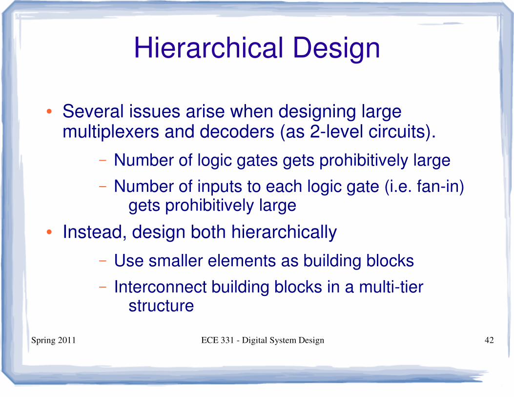
Hierarchical Design
● Several issues arise when designing large multiplexers and decoders (as 2-level circuits).
– Number of logic gates gets prohibitively large
– Number of inputs to each logic gate (i.e. fan-in) gets prohibitively large
● Instead, design both hierarchically
– Use smaller elements as building blocks
– Interconnect building blocks in a multi-tier structure
Spring 2011 ECE 331 - Digital System Design 43
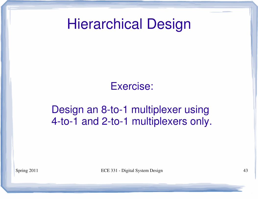
Hierarchical Design
Exercise:
Design an 8-to-1 multiplexer using 4-to-1 and 2-to-1 multiplexers only.
Spring 2011 ECE 331 - Digital System Design 44
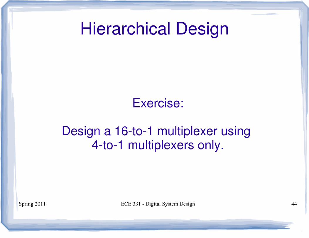
Hierarchical Design
Exercise:
Design a 16-to-1 multiplexer using 4-to-1 multiplexers only.
Spring 2011 ECE 331 - Digital System Design 45
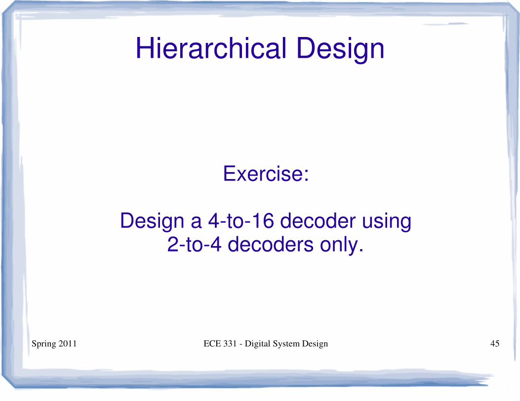
Hierarchical Design
Exercise:
Design a 4-to-16 decoder using2-to-4 decoders only.
Spring 2011 ECE 331 - Digital System Design 46
Questions?