e-space 20 final project review report 1 magnetic resonant coils offer a mid range, yet still...
TRANSCRIPT
Team 20 Final Project Review Report
1
Abstract—The current implementation of wireless power
transfer uses inductive power transfer, involving strongly coupled
coils and high efficiency, close range transfer. This technology
only works with ranges less than a few centimeters, and the coils
must be orientated correctly to affect efficient power transfer. A
different technology known as Magnetic Resonant Power
Transfer has emerged that promises mid range, yet still high
efficiency power transfer. The transmitting and receiving coils
are loosely coupled, meaning the distance between them and their
relative orientation is much more flexible, but resonate at a fixed
frequency that still facilitates efficient transfer between them.
Using this technology we are implementing a wireless power
transfer system to charge a wireless phone at farther ranges than
is possible with inductive technology.
I. INTRODUCTION
Since the 1970’s, transistor count and computing speed has
followed Moore’s law, doubling every 18 months. However in
that time, battery technology has lagged far behind, with
energy density only doubling between 1980 and 2010 [1]. This
and the proliferation of devices including smartphones, tablets,
and laptops, has led to a major problem in keeping devices
charged while living an increasingly mobile life. Public
locations like airports, parks, and college campuses include
built-in charging stations for mobile devices or banks of
outlets in their designs. The need for charging cables and ports
is also an inherent weakness in electronics design. The internal
electronics must be open and exposed to allow charging cables
to connect. These ports put a limitation of how shock, dust,
and waterproof devices can be.
However, what if devices could charge automatically
without a need for ports or charging cables? This possibility
has been explored with inductive charging pads. Inductive
chargers offer high efficiency, but the transmitting and
receiving coils need to be equally sized and oriented such that
all the magnetic flux transmitted must be received. Such pads
solve the problem of relying on cables and connectors, but the
limited range of only a few centimeters and stringent
orientation requirements mean that this technology can only be
used while the device is stationary and thus batteries still need
to be large and abundant.
J. D. Scharf from Plainview, NY (e-mail: [email protected]).
S. Pietryka from Sandwich, MA (e-mail: [email protected]).
S. Bevacqua from Falmouth, MA (e-mail: [email protected]).
Magnetic Resonant Coils offer a mid range, yet still efficient
solution to this problem. The transmitting and receiving coils
resonate at a fixed frequency, resulting in a high quality factor.
This quality factor makes up for the fact that the coils have a
lower coupling factor due to increased ranges and non-ideal
relative coil orientations. The resonant fields can also charge
multiple devices at once without requiring direct line of sight
to the receiving devices. Ranges of two meters have been
successfully demonstrated, meaning this technology could in
the future be used to directly power devices or charge devices
as one moves around, resulting in a diminished need for
batteries [2].
This technology has important applications other than
consumer electronics. This technology could revolutionize
medical implants since the devices could be charged wirelessly
from outside the body, instead of requiring invasive surgeries
to replace batteries. It also has applications in the
transportation industry as electric vehicles become more
popular. Charging coils can be embedded in parking lots, bus
stops, and even the road to charge vehicles at all times,
effectively increasing the range and up-time of these vehicles.
Since this technology is still primarily a research topic, the
modest application of charging a mobile phone was chosen.
The solution will involve a transmitter that will be mounted to
the bottom of a desk and will be able to supply power to the
receiving coil, located in a phone case, 1 cm above the desk
and 1cm below the desk. The iPhone 4 will be utilized, placing
a limit on the size of the receiving coil to a maximum of 10.5
cm by 5.86 cm. The transmitting coil has no size restrictions.
The input power will be limited by the standard wall output of
120 VAC at 60 Hz. The maximum allowed electric and
magnetic fields are determined by the IEEE [3]. The
specifications are listed in Table 1.
II. DESIGN
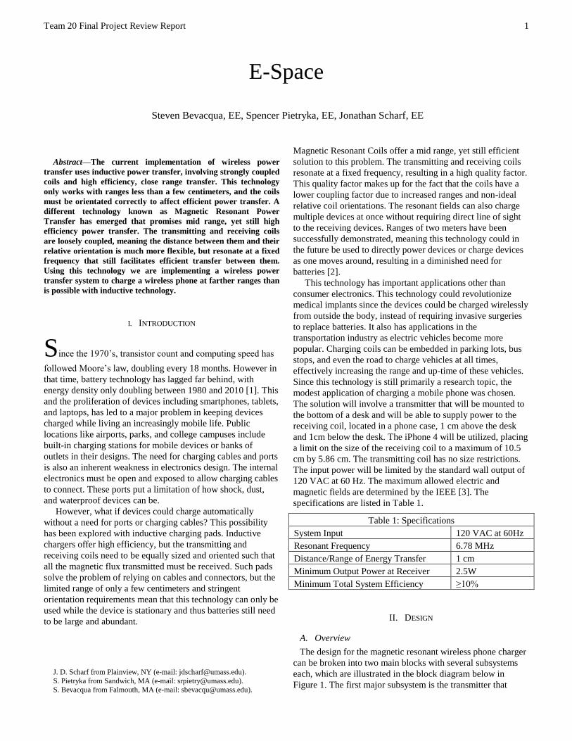
A. Overview
The design for the magnetic resonant wireless phone charger
can be broken into two main blocks with several subsystems
each, which are illustrated in the block diagram below in
Figure 1. The first major subsystem is the transmitter that
E-Space
Steven Bevacqua, EE, Spencer Pietryka, EE, Jonathan Scharf, EE
Table 1: Specifications
System Input 120 VAC at 60Hz
Resonant Frequency 6.78 MHz
Distance/Range of Energy Transfer 1 cm
Minimum Output Power at Receiver 2.5W
Minimum Total System Efficiency ≥10%
Team 20 Final Project Review Report
2
consists of a power supply, an oscillator, an amplifier,
impedance matching network, and a resonant coil. The
transmitter coil and circuitry are enclosed within a plastic case
that can be attached underneath a desk or any other location
desired by the user. The receiver consists of a resonant coil, an
impedance matching network, a rectifier, and voltage
regulator. A phone case will be 3D printed and the receiver
coil and circuitry will be placed inside. A small USB cable
will then connect the phone to the output of the voltage
regulator to charge the phone. Additionally, there is also the
option to include a repeater located at some point between the
transmitter and receiver. A repeater is another coil that is tuned
to the same resonant frequency as the transmitter and receiver
coils, which can help to improve distance and efficiency of the
power transfer [4]. However, we did not use a repeater in the
final design.
Figure 1. Block Diagram
The block diagram shows the subsections of the two major
blocks used for the phone charger as well as division of labor
among the team. The following descriptions outline each
subsection as well as the technology used to create and test
them before implementation.
B. Power Supply
A power supply or AC/DC converter is the first step in the
block diagram because it is used to power the oscillator,
voltage buffer, and power amplifier on the transmitter. AC
power directly from the wall operates around 50-60 Hz, which
is much lower than the resonant frequency of the coils. Instead
of directly converting the frequency from 60 Hz to 6.78 MHz,
the AC wall power will be converted to DC with the power
supply and then used to power the oscillator at the resonant
frequency of the coils. To meet the 10 percent efficiency
specification at the maximum distance while supplying 2.5 W
to the phone, the required power supply will need to be able to
source at least ten times the output power. Therefore, we
selected a 60W computer power supply, CUI Inc. ETSA 60W
UD [5]. The power supply converts the 120VAC input to a
12V output at 5A maximum. The supply output was selected
based on the operating voltage of the power amplifier at about
12V. The oscillator and voltage buffer use lower voltages,
which were achieved using a switching voltage regulator.
C. Switching Voltage Regulators
On the transmitter, the oscillator and voltage buffer require a
supply voltage that is less than the output of the wall power
supply. The two ICs have an overlapping supply voltage of
3.3V, so a voltage regulator was used to convert the 12V
power supply output to 3.3V. The voltage regulator on the
transmitter is Texas Instruments’ LM2594N-3.3, which can
take a 4.5V-40V input and produce an output of 3.3V at
500mA maximum [6].
Another voltage regulator was used on the receiver to
convert the unregulated DC signal from the rectifier to the
proper voltage for USB charging. We used a Texas
Instruments’ LM2575T-5.0 that accepts a 4V-40V input and
has a 5V output at up to 1A [7]. The wide input voltage range
is important because the rectified signal on the receiver varies
as the distance between the transmitter and receiver coils
changes. Additionally, both voltage regulators used are
switching regulators because they have improved efficiency
over linear regulators.
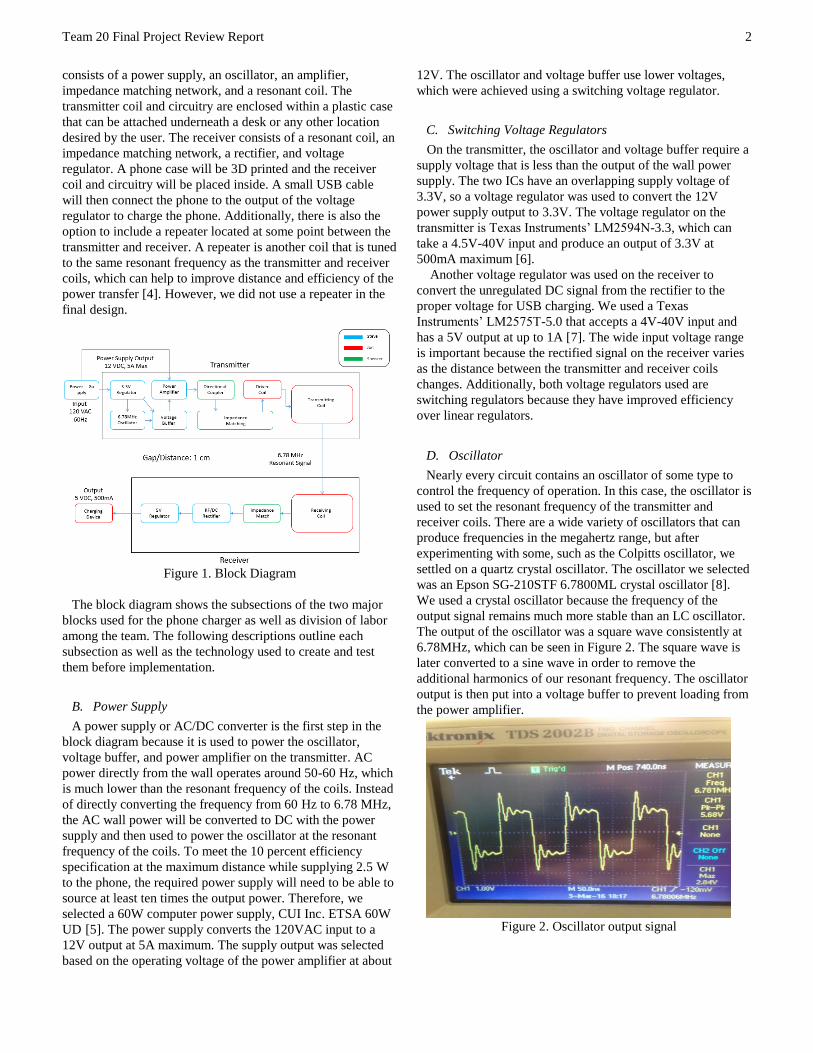
D. Oscillator
Nearly every circuit contains an oscillator of some type to
control the frequency of operation. In this case, the oscillator is
used to set the resonant frequency of the transmitter and
receiver coils. There are a wide variety of oscillators that can
produce frequencies in the megahertz range, but after
experimenting with some, such as the Colpitts oscillator, we
settled on a quartz crystal oscillator. The oscillator we selected
was an Epson SG-210STF 6.7800ML crystal oscillator [8].
We used a crystal oscillator because the frequency of the
output signal remains much more stable than an LC oscillator.
The output of the oscillator was a square wave consistently at
6.78MHz, which can be seen in Figure 2. The square wave is
later converted to a sine wave in order to remove the
additional harmonics of our resonant frequency. The oscillator
output is then put into a voltage buffer to prevent loading from
the power amplifier.
Figure 2. Oscillator output signal
Team 20 Final Project Review Report
3
E. Voltage Buffer
As mentioned above in the oscillator section, operating at the
resonant frequency is crucial for the technology to work
optimally. By loading the output of the oscillator, the
frequency can shift away from resonance or even attenuate the
oscillating signal. To prevent this from happening, a voltage
buffer is placed at the output of the oscillator before the power
amplifier. Typical op amp ICs can be configured to a buffer
where the gain is close to 1, however because we are operating
at a high frequency, a buffer amplifier with a higher bandwidth
was chosen. The selected buffer is the Texas Instruments
BUF634P, which has an option for up to 180MHz 3dB
bandwidth [9]. Additionally, the slew rate limit of the buffer
changes the square wave from the oscillator to a triangular
waveform. Although a slew rate limit is usually yields poor
results, it seems to have been a benefit for our application.
Finally, before the output signal is fed to the power amplifier,
it is passed through a resistive voltage divider to change the
input power to the amplifier.
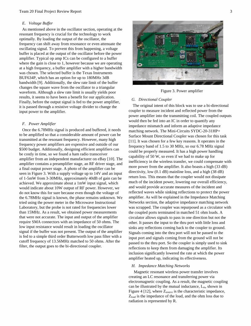
F. Power Amplifier
Once the 6.78MHz signal is produced and buffered, it needs
to be amplified so that a considerable amount of power can be
transmitted at the resonant frequency. However, many high
frequency power amplifiers are expensive and outside of our
$500 budget. Additionally, designing efficient amplifiers can
be costly in time, so we found a ham radio transceiver
amplifier from an independent manufacturer on eBay [10]. The
amplifier contains a preamplifier stage, an RF driver stage, and
a final output power stage. A photo of the amplifier can be
seen in Figure 3. With a supply voltage up to 14V and an input
of 1-5mW from 3-30MHz, approximately 40dB of gain can be
achieved. We approximate about a 1mW input signal, which
would indicate about 10W output of RF power. However, we
do not know this for sure because even though the voltage of
the 6.78MHz signal is known, the phase remains unknown. We
tried using the power meter in the Microwave Instructional
Laboratory, but the probe is not rated for frequencies lower
than 15MHz. As a result, we obtained power measurements
that were not accurate. The input and output of the amplifier
require SMA connectors with an impedance of 50 ohms. The
low input resistance would result in loading the oscillator
signal if the buffer was not present. The output of the amplifier
is fed to a simple third order Butterworth low pass filter with a
cutoff frequency of 13.56MHz matched to 50 ohms. After the
filter, the output goes to the bi-directional coupler.
Figure 3. Power amplifier
G. Directional Coupler
The original intent of this block was to use a bi-directional
coupler to measure incident and reflected power from the
power amplifier into the transmitting coil. The coupled outputs
would then be fed into an IC in order to quantify any
impedance mismatch and inform an adaptive impedance
matching network. The Mini-Circuits SYDC-20-31HP+
Surface Mount Directional Coupler was chosen for this task
[11]. It was chosen for a few key reasons. It operates in the
frequency band of 1.5 to 30 MHz, so our 6.78 MHz signal
could be properly measured. It has a high power handling
capability of 50 W, so even if we had to make up for
inefficiency in the wireless transfer, we could compensate with
more power from the amplifier. It also boasts a high (33 dB)
directivity, low (0.1 dB) mainline loss, and a high (38 dB)
return loss. This means that the coupler would not dissipate
much of the incident power, lowering our overall efficiency,
and would provide accurate measures of the incident and
reflected waves while sinking reflections to protect the power
amplifier. As will be explained in the Impedance Matching
Networks section, the adaptive impedance matching network
was scrapped. The coupler was repurposed as a circulator with
the coupled ports terminated in matched 51 ohm loads. A
circulator allows signals to pass in one direction but not the
other. It passes the input to the thru port with little loss and
sinks any reflections coming back to the coupler to ground.
Signals coming into the thru port will not be passed to the
input port and signals coming from the ground will not be
passed to the thru port. So the coupler is simply used to sink
reflections to keep them from damaging the amplifier. Its
inclusion significantly lowered the rate at which the power
amplifier heated up, indicating its effectiveness.
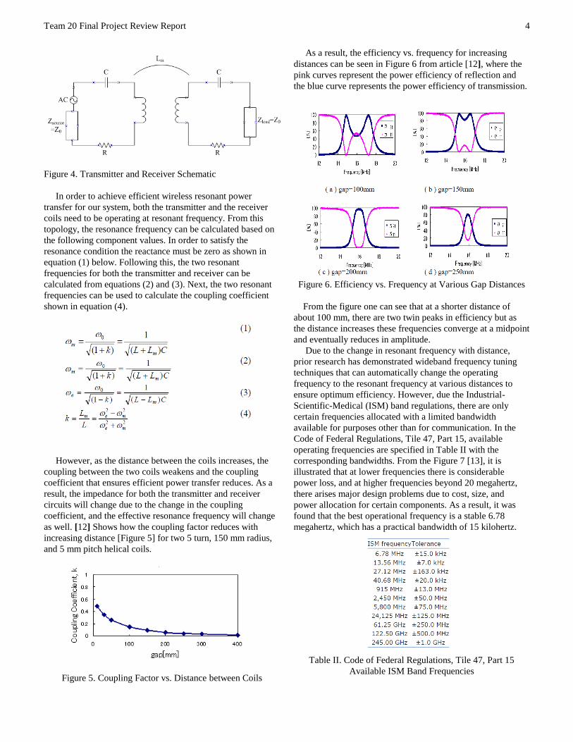
H. Impedance Matching Networks
Magnetic resonant wireless power transfer involves
creating an LC resonance and transferring power via
electromagnetic coupling. As a result, the magnetic coupling
can be illustrated by the mutual inductance, Lm, shown in
Figure 4 [12], where Zsource is the characteristic impedance,
Zload is the impedance of the load, and the ohm loss due to
radiation is represented by R.
Team 20 Final Project Review Report
4
Figure 4. Transmitter and Receiver Schematic
In order to achieve efficient wireless resonant power
transfer for our system, both the transmitter and the receiver
coils need to be operating at resonant frequency. From this
topology, the resonance frequency can be calculated based on
the following component values. In order to satisfy the
resonance condition the reactance must be zero as shown in
equation (1) below. Following this, the two resonant
frequencies for both the transmitter and receiver can be
calculated from equations (2) and (3). Next, the two resonant
frequencies can be used to calculate the coupling coefficient
shown in equation (4).
However, as the distance between the coils increases, the
coupling between the two coils weakens and the coupling
coefficient that ensures efficient power transfer reduces. As a
result, the impedance for both the transmitter and receiver
circuits will change due to the change in the coupling
coefficient, and the effective resonance frequency will change
as well. [12] Shows how the coupling factor reduces with
increasing distance [Figure 5] for two 5 turn, 150 mm radius,
and 5 mm pitch helical coils.
Figure 5. Coupling Factor vs. Distance between Coils
As a result, the efficiency vs. frequency for increasing
distances can be seen in Figure 6 from article [12], where the
pink curves represent the power efficiency of reflection and
the blue curve represents the power efficiency of transmission.
Figure 6. Efficiency vs. Frequency at Various Gap Distances
From the figure one can see that at a shorter distance of
about 100 mm, there are two twin peaks in efficiency but as
the distance increases these frequencies converge at a midpoint
and eventually reduces in amplitude.
Due to the change in resonant frequency with distance,
prior research has demonstrated wideband frequency tuning
techniques that can automatically change the operating
frequency to the resonant frequency at various distances to
ensure optimum efficiency. However, due the Industrial-
Scientific-Medical (ISM) band regulations, there are only
certain frequencies allocated with a limited bandwidth
available for purposes other than for communication. In the
Code of Federal Regulations, Tile 47, Part 15, available
operating frequencies are specified in Table II with the
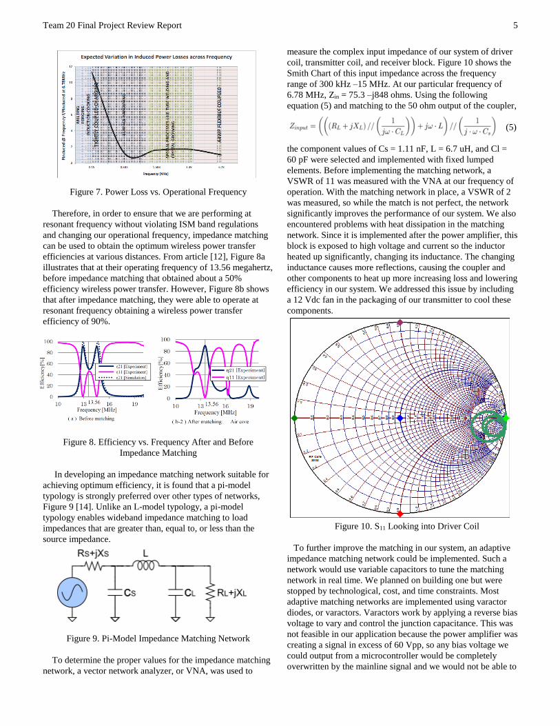
corresponding bandwidths. From the Figure 7 [13], it is
illustrated that at lower frequencies there is considerable
power loss, and at higher frequencies beyond 20 megahertz,
there arises major design problems due to cost, size, and
power allocation for certain components. As a result, it was
found that the best operational frequency is a stable 6.78
megahertz, which has a practical bandwidth of 15 kilohertz.
Table II. Code of Federal Regulations, Tile 47, Part 15
Available ISM Band Frequencies
Team 20 Final Project Review Report
5
Figure 7. Power Loss vs. Operational Frequency
Therefore, in order to ensure that we are performing at
resonant frequency without violating ISM band regulations
and changing our operational frequency, impedance matching
can be used to obtain the optimum wireless power transfer
efficiencies at various distances. From article [12], Figure 8a
illustrates that at their operating frequency of 13.56 megahertz,
before impedance matching that obtained about a 50%
efficiency wireless power transfer. However, Figure 8b shows
that after impedance matching, they were able to operate at
resonant frequency obtaining a wireless power transfer
efficiency of 90%.
Figure 8. Efficiency vs. Frequency After and Before
Impedance Matching
In developing an impedance matching network suitable for
achieving optimum efficiency, it is found that a pi-model
typology is strongly preferred over other types of networks,
Figure 9 [14]. Unlike an L-model typology, a pi-model
typology enables wideband impedance matching to load
impedances that are greater than, equal to, or less than the
source impedance.
Figure 9. Pi-Model Impedance Matching Network
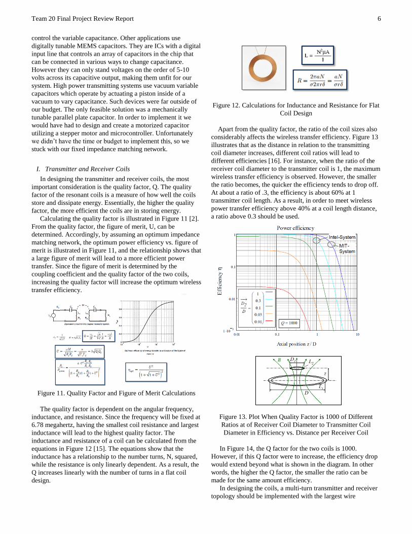
To determine the proper values for the impedance matching
network, a vector network analyzer, or VNA, was used to
measure the complex input impedance of our system of driver
coil, transmitter coil, and receiver block. Figure 10 shows the
Smith Chart of this input impedance across the frequency
range of 300 kHz –15 MHz. At our particular frequency of
6.78 MHz, Zin = 75.3 –j848 ohms. Using the following
equation (5) and matching to the 50 ohm output of the coupler,
(5)
the component values of Cs = 1.11 nF, L = 6.7 uH, and Cl =
60 pF were selected and implemented with fixed lumped
elements. Before implementing the matching network, a
VSWR of 11 was measured with the VNA at our frequency of
operation. With the matching network in place, a VSWR of 2
was measured, so while the match is not perfect, the network
significantly improves the performance of our system. We also
encountered problems with heat dissipation in the matching
network. Since it is implemented after the power amplifier, this
block is exposed to high voltage and current so the inductor
heated up significantly, changing its inductance. The changing
inductance causes more reflections, causing the coupler and
other components to heat up more increasing loss and lowering
efficiency in our system. We addressed this issue by including
a 12 Vdc fan in the packaging of our transmitter to cool these
components.
Figure 10. S11 Looking into Driver Coil
To further improve the matching in our system, an adaptive
impedance matching network could be implemented. Such a
network would use variable capacitors to tune the matching
network in real time. We planned on building one but were
stopped by technological, cost, and time constraints. Most
adaptive matching networks are implemented using varactor
diodes, or varactors. Varactors work by applying a reverse bias
voltage to vary and control the junction capacitance. This was
not feasible in our application because the power amplifier was
creating a signal in excess of 60 Vpp, so any bias voltage we
could output from a microcontroller would be completely
overwritten by the mainline signal and we would not be able to
Team 20 Final Project Review Report
6
control the variable capacitance. Other applications use
digitally tunable MEMS capacitors. They are ICs with a digital
input line that controls an array of capacitors in the chip that
can be connected in various ways to change capacitance.
However they can only stand voltages on the order of 5-10
volts across its capacitive output, making them unfit for our
system. High power transmitting systems use vacuum variable
capacitors which operate by actuating a piston inside of a
vacuum to vary capacitance. Such devices were far outside of
our budget. The only feasible solution was a mechanically
tunable parallel plate capacitor. In order to implement it we
would have had to design and create a motorized capacitor
utilizing a stepper motor and microcontroller. Unfortunately
we didn’t have the time or budget to implement this, so we
stuck with our fixed impedance matching network.
I. Transmitter and Receiver Coils
In designing the transmitter and receiver coils, the most
important consideration is the quality factor, Q. The quality
factor of the resonant coils is a measure of how well the coils
store and dissipate energy. Essentially, the higher the quality
factor, the more efficient the coils are in storing energy.
Calculating the quality factor is illustrated in Figure 11 [2].
From the quality factor, the figure of merit, U, can be
determined. Accordingly, by assuming an optimum impedance
matching network, the optimum power efficiency vs. figure of
merit is illustrated in Figure 11, and the relationship shows that
a large figure of merit will lead to a more efficient power
transfer. Since the figure of merit is determined by the
coupling coefficient and the quality factor of the two coils,
increasing the quality factor will increase the optimum wireless
transfer efficiency.
Figure 11. Quality Factor and Figure of Merit Calculations
The quality factor is dependent on the angular frequency,
inductance, and resistance. Since the frequency will be fixed at
6.78 megahertz, having the smallest coil resistance and largest
inductance will lead to the highest quality factor. The
inductance and resistance of a coil can be calculated from the
equations in Figure 12 [15]. The equations show that the
inductance has a relationship to the number turns, N, squared,
while the resistance is only linearly dependent. As a result, the
Q increases linearly with the number of turns in a flat coil
design.
Figure 12. Calculations for Inductance and Resistance for Flat
Coil Design
Apart from the quality factor, the ratio of the coil sizes also
considerably affects the wireless transfer efficiency. Figure 13
illustrates that as the distance in relation to the transmitting
coil diameter increases, different coil ratios will lead to
different efficiencies [16]. For instance, when the ratio of the
receiver coil diameter to the transmitter coil is 1, the maximum
wireless transfer efficiency is observed. However, the smaller
the ratio becomes, the quicker the efficiency tends to drop off.
At about a ratio of .3, the efficiency is about 60% at 1
transmitter coil length. As a result, in order to meet wireless
power transfer efficiency above 40% at a coil length distance,
a ratio above 0.3 should be used.
Figure 13. Plot When Quality Factor is 1000 of Different
Ratios at of Receiver Coil Diameter to Transmitter Coil
Diameter in Efficiency vs. Distance per Receiver Coil
In Figure 14, the Q factor for the two coils is 1000.
However, if this Q factor were to increase, the efficiency drop
would extend beyond what is shown in the diagram. In other
words, the higher the Q factor, the smaller the ratio can be
made for the same amount efficiency.
In designing the coils, a multi-turn transmitter and receiver
topology should be implemented with the largest wire
Team 20 Final Project Review Report
7
thickness possible for the fitted area to obtain a smaller
resistance. Additionally, a receiver to transmitter diameter coil
ratio should be greater than 0.3 to ensure that the efficiency
doesn’t drop off considerably at shorter distances. To test the
quality factor of the coils, an LCR parameter analyzer is used.
The receiver coil diameter and size is limited to the area of
the phone or the phone case (Figure 14). As a result, the
transmitter coil diameter is limited to approximately 175 mm
or approximately three times the width of the phone when
taking into account the efficiency drop off from the ratio of
receiver sizes mentioned in [16] and shown in Figure 12.
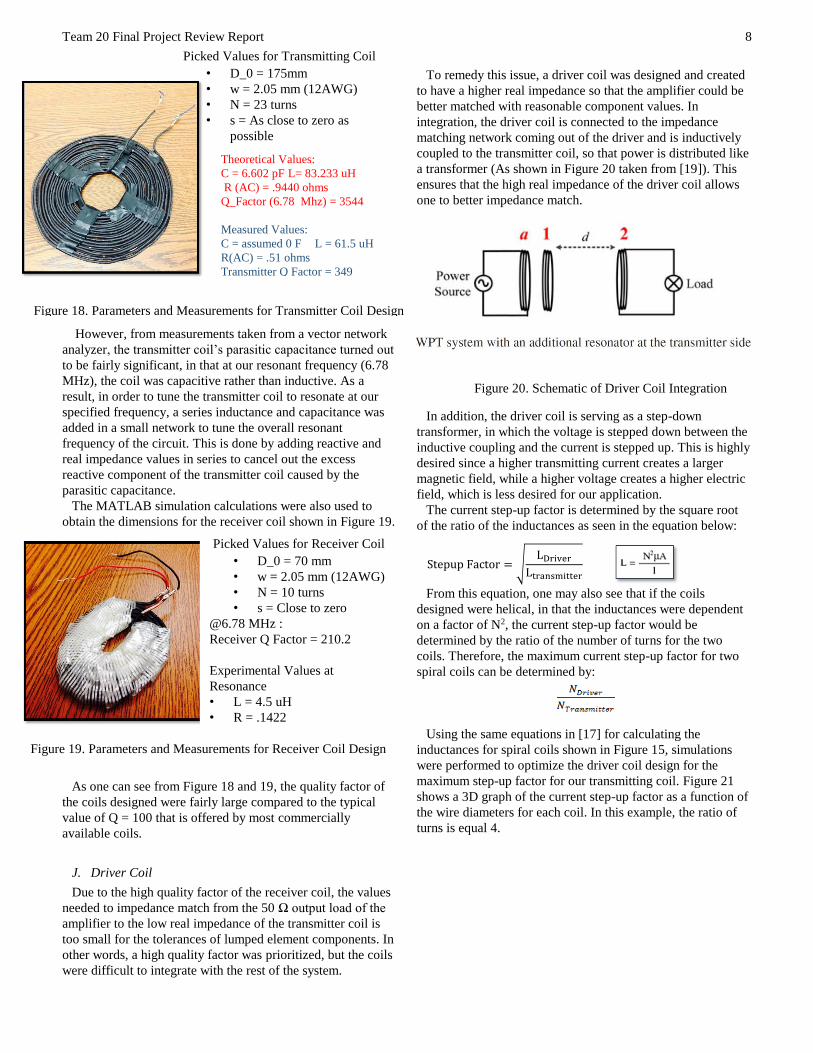
In order to maximize the Q-factor for both the transmitter
and receiver coils for their respective sizes, simulations were
performed for the optimal number of turns, wire diameter, and
diameter length for the design. Using the equations given from
[17] shown in Figure 15, a simulation was performed on the
quality factor’s dependence on the key parameters mentioned
previously.
After simulation, it was found that for the frequency and turn
spacing, the effects on the quality factor are fairly linear, in
that in order to get the highest quality factor, one would want a
higher frequency and a smaller spacing between the wires.
Therefore, the following three 3D graphs in Figure 16 were
created to optimize the number of turns, outer diameter size,
and wire diameter for the transmitter coil.
In addition to the quality factor, a simulation was also
performed for the coupling coefficient from [18]. From the
resulting MATLAB plot from Figure 17, it can be see that the
coupling coefficient with respect to distance matches well with
the theory of drop off in coupling over distance.
From these plots, the transmitting coil was designed, such
that the maximum quality factor was achieved. From Figure
18, it can be seen the values predicted matched closely with
the values calculated, although the Q-factor was over
estimated since the equations did not take into account the
parabolic nature of the quality factor with frequency. However,
the parameters, L and R, were optimized, which is what results
in a high magnitude quality factor.
Figure 14. Dimensions for standard IPhone 4
Figure 15. Computational model and equations of spiral coil
based on various parameters, where: N is the number of turns, D_0 is the outer diameter, p is the spacing between
turns, w is the wire diameter, D_i is the inner diameter, l is the total wire length,
α is the winding radius, c is the radial depth, and f is the resonant frequency
Figure 16. MATLAB Simulation plots
Figure 16. Equations and MATLAB Simulation
for Calculating Coupling Coefficient
Team 20 Final Project Review Report
8
Picked Values for Transmitting Coil
• D_0 = 175mm
• w = 2.05 mm (12AWG)
• N = 23 turns
• s = As close to zero as
possible
However, from measurements taken from a vector network
analyzer, the transmitter coil’s parasitic capacitance turned out
to be fairly significant, in that at our resonant frequency (6.78
MHz), the coil was capacitive rather than inductive. As a
result, in order to tune the transmitter coil to resonate at our
specified frequency, a series inductance and capacitance was
added in a small network to tune the overall resonant
frequency of the circuit. This is done by adding reactive and
real impedance values in series to cancel out the excess
reactive component of the transmitter coil caused by the
parasitic capacitance.
The MATLAB simulation calculations were also used to
obtain the dimensions for the receiver coil shown in Figure 19.
As one can see from Figure 18 and 19, the quality factor of
the coils designed were fairly large compared to the typical
value of Q = 100 that is offered by most commercially
available coils.
J. Driver Coil
Due to the high quality factor of the receiver coil, the values
needed to impedance match from the 50 Ω output load of the
amplifier to the low real impedance of the transmitter coil is
too small for the tolerances of lumped element components. In
other words, a high quality factor was prioritized, but the coils
were difficult to integrate with the rest of the system.
To remedy this issue, a driver coil was designed and created
to have a higher real impedance so that the amplifier could be
better matched with reasonable component values. In
integration, the driver coil is connected to the impedance
matching network coming out of the driver and is inductively
coupled to the transmitter coil, so that power is distributed like
a transformer (As shown in Figure 20 taken from [19]). This
ensures that the high real impedance of the driver coil allows
one to better impedance match.
In addition, the driver coil is serving as a step-down
transformer, in which the voltage is stepped down between the
inductive coupling and the current is stepped up. This is highly
desired since a higher transmitting current creates a larger
magnetic field, while a higher voltage creates a higher electric
field, which is less desired for our application.
The current step-up factor is determined by the square root
of the ratio of the inductances as seen in the equation below:
From this equation, one may also see that if the coils
designed were helical, in that the inductances were dependent
on a factor of N2, the current step-up factor would be
determined by the ratio of the number of turns for the two
coils. Therefore, the maximum current step-up factor for two
spiral coils can be determined by:
Using the same equations in [17] for calculating the
inductances for spiral coils shown in Figure 15, simulations
were performed to optimize the driver coil design for the
maximum step-up factor for our transmitting coil. Figure 21
shows a 3D graph of the current step-up factor as a function of
the wire diameters for each coil. In this example, the ratio of
turns is equal 4.
Theoretical Values:
C = 6.602 pF L= 83.233 uH
R (AC) = .9440 ohms
Q_Factor (6.78 Mhz) = 3544
Measured Values:
C = assumed 0 F L = 61.5 uH
R(AC) = .51 ohms
Transmitter Q Factor = 349
Figure 18. Parameters and Measurements for Transmitter Coil Design
Figure 19. Parameters and Measurements for Receiver Coil Design
Picked Values for Receiver Coil
• D_0 = 70 mm
• w = 2.05 mm (12AWG)
• N = 10 turns
• s = Close to zero
@6.78 MHz :
Receiver Q Factor = 210.2
Experimental Values at
Resonance
• L = 4.5 uH
• R = .1422
Figure 20. Schematic of Driver Coil Integration
Team 20 Final Project Review Report
9
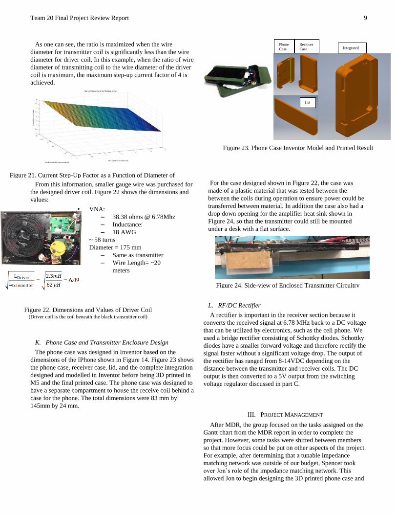
As one can see, the ratio is maximized when the wire
diameter for transmitter coil is significantly less than the wire
diameter for driver coil. In this example, when the ratio of wire
diameter of transmitting coil to the wire diameter of the driver
coil is maximum, the maximum step-up current factor of 4 is
achieved.
From this information, smaller gauge wire was purchased for
the designed driver coil. Figure 22 shows the dimensions and
values:
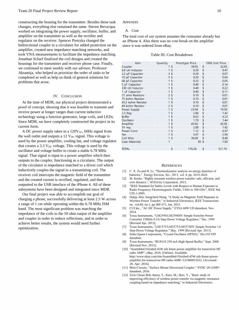
K. Phone Case and Transmitter Enclosure Design
The phone case was designed in Inventor based on the
dimensions of the IPhone shown in Figure 14. Figure 23 shows
the phone case, receiver case, lid, and the complete integration
designed and modelled in Inventor before being 3D printed in
M5 and the final printed case. The phone case was designed to
have a separate compartment to house the receive coil behind a
case for the phone. The total dimensions were 83 mm by
145mm by 24 mm.
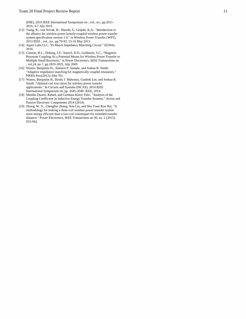
For the case designed shown in Figure 22, the case was
made of a plastic material that was tested between the
between the coils during operation to ensure power could be
transferred between material. In addition the case also had a
drop down opening for the amplifier heat sink shown in
Figure 24, so that the transmitter could still be mounted
under a desk with a flat surface.
L. RF/DC Rectifier
A rectifier is important in the receiver section because it
converts the received signal at 6.78 MHz back to a DC voltage
that can be utilized by electronics, such as the cell phone. We
used a bridge rectifier consisting of Schottky diodes. Schottky
diodes have a smaller forward voltage and therefore rectify the
signal faster without a significant voltage drop. The output of
the rectifier has ranged from 8-14VDC depending on the
distance between the transmitter and receiver coils. The DC
output is then converted to a 5V output from the switching
voltage regulator discussed in part C.
III. PROJECT MANAGEMENT
After MDR, the group focused on the tasks assigned on the
Gantt chart from the MDR report in order to complete the
project. However, some tasks were shifted between members
so that more focus could be put on other aspects of the project.
For example, after determining that a tunable impedance
matching network was outside of our budget, Spencer took
over Jon’s role of the impedance matching network. This
allowed Jon to begin designing the 3D printed phone case and
Figure 21. Current Step-Up Factor as a Function of Diameter of
Coils
• VNA:
– 38.38 ohms @ 6.78Mhz
– Inductance:
– 18 AWG
• ~ 58 turns
• Diameter = 175 mm
– Same as transmitter
– Wire Length= ~20
meters
Receiver
Case
Phone
Case
Lid
Integrated
Figure 23. Phone Case Inventor Model and Printed Result
Figure 24. Side-view of Enclosed Transmitter Circuitry
Figure 22. Dimensions and Values of Driver Coil (Driver coil is the coil beneath the black transmitter coil)
Team 20 Final Project Review Report
10
constructing the housing for the transmitter. Besides these task
changes, everything else remained the same. Steven Bevacqua
worked on integrating the power supply, oscillator, buffer, and
amplifier on the transmitter as well as the rectifier and
regulator on the receiver. Spencer Pietryka changed the
bidirectional coupler to a circulator for added protection on the
amplifier, created new impedance matching networks, and
took VNA measurements to facilitate the impedance matching.
Jonathan Scharf finalized the coil designs and created the
housings for the transmitter and receiver phone case. Finally,
we continued to meet weekly with our advisor, Professor
Aksamija, who helped us prioritize the order of tasks to be
completed as well as help us think of general solutions for
problems that arose.
IV. CONCLUSION
At the time of MDR, our physical project demonstrated a
proof of concept, showing that it was feasible to transmit and
receive power at longer ranges than current inductive
technology using a function generator, large coils, and LEDs.
Since MDR, we have completely constructed the project in its
current form.
A DC power supply takes in a 120VAC, 60Hz signal from
the wall outlet and outputs a 12 VDC signal. This voltage is
used by the power amplifier, cooling fan, and voltage regulator
that creates a 3.3 VDC voltage. This voltage is used by the
oscillator and voltage buffer to create a stable 6.78 MHz
signal. That signal is input to a power amplifier which then
outputs to the coupler, functioning as a circulator. The output
of the circulator is impedance matched to a driver coil which
inductively couples the signal to a transmitting coil. The
receiver coil intercepts the magnetic field of the transmitter
and the created current is rectified, regulated, and then
outputted to the USB interface of the iPhone 4. All of these
subsystems have been designed and integrated since MDR.
Our final project was able to accomplish our goal of
charging a phone, successfully delivering at least 2.5 W across
a range of 1 cm while operating within the 6.78 MHz ISM
band. The most significant problem was matching the
impedance of the coils to the 50 ohm output of the amplifier
and coupler in order to reduce reflections, and in order to
achieve better results, the system would need further
optimization.
APPENDIX
A. Cost
The total cost of our system assumes the consumer already has
an iPhone 4. Also there was no cost break on the amplifier
since it was ordered from eBay.
Table III. Cost Breakdown
REFERENCES
[1] C. X. Zu and H. Li, “Thermodynamic analysis on energy densities of
batteries,” Energy Environ. Sci., 2011, vol. 4, pp. 2614-2624
[2] M. Kesler, "Highly resonant wireless power transfer: safe, efficient, and
over distance.", WiTricity Corporation. 2013.
[3] “IEEE Standard for Safety Levels with Respect to Human Exposure to
Radio Frequency Electromagnetic Fields, 3 kHz to 300 GHz”, IEEE Std.
C95.1-2005.
[4] Dukju Ahn; Songcheol Hong, "A Study on Magnetic Field Repeater in
Wireless Power Transfer," in Industrial Electronics, IEEE Transactions
on , vol.60, no.1, pp.360-371, Jan. 2013
[5] CUI Inc., “AC-DC Power Supply,” ETSA 60W UD datasheet, Nov.
2014.
[6] Texas Instruments, “LM2594/LM2594HV Simple Switcher Power
Converter 150kHz 0.5A Step-Down Voltage Regulator,” Dec. 1999
[Revised Apr. 2013].
[7] Texas Instruments, “LM1575/LM2575/LM3575HV Simple Switcher 1A
Step-Down Voltage Regulator,” May. 1999 [Revised Apr. 2013].
[8] Seiko Epson Corporation, “Crystal Oscillator (SPXO),” SG-210 STF
datasheet.
[9] Texas Instruments, “BUF634 250-mA High-Speed Buffer,” Sept. 2000
[Revised Nov. 2015].
[10] "Assembled Finished 45W ssb linear power amplifier for transceiver HF
radio AMP", eBay, 2016. [Online]. Available:
http://www.ebay.com/itm/Assembled-Finished-45W-ssb-linear-power-
amplifier-for-transceiver-HF-radio-AMP-/121960051022. [Accessed:
28- Apr- 2016].
[11] Mini-Circuits, “Surface Mount Directional Coupler,” SYDC-20-31HP+
datasheet, 2016
[12] Teck Chuan Beh; Imura, T.; Kato, M.; Hori, Y., "Basic study of
improving efficiency of wireless power transfer via magnetic resonance
coupling based on impedance matching," in Industrial Electronics
Team 20 Final Project Review Report
11
(ISIE), 2010 IEEE International Symposium on , vol., no., pp.2011-
2016, 4-7 July 2010
[13] Tseng, R.; von Novak, B.; Shevde, S.; Grajski, K.A., "Introduction to
the alliance for wireless power loosely-coupled wireless power transfer
system specification version 1.0," in Wireless Power Transfer (WPT),
2013 IEEE , vol., no., pp.79-83, 15-16 May 2013
[14] Aspen Labs LLC, "Pi-Match Impedance Matching Circuit." EEWeb,
2016.
[15] Cannon, B.L.; Hoburg, J.F.; Stancil, D.D.; Goldstein, S.C., "Magnetic
Resonant Coupling As a Potential Means for Wireless Power Transfer to
Multiple Small Receivers," in Power Electronics, IEEE Transactions on
, vol.24, no.7, pp.1819-1825, July 2009
[16] Waters, Benjamin H., Alanson P. Sample, and Joshua R. Smith.
"Adaptive impedance matching for magnetically coupled resonators."
PIERS Proc(2012): 694-701.
[17] Waters, Benjamin H., Brody J. Mahoney, Gunbok Lee, and Joshua R.
Smith. "Optimal coil size ratios for wireless power transfer
applications." In Circuits and Systems (ISCAS), 2014 IEEE
International Symposium on, pp. 2045-2048. IEEE, 2014.
[18] Mendes Duarte, Rafael, and Gordana Klaric Felic. "Analysis of the
Coupling Coefficient in Inductive Energy Transfer Systems." Active and
Passive Electronic Components 2014 (2014).
[19] Zhong, W. X., Chenghui Zhang, Xun Liu, and Shu Yuen Ron Hui. "A
methodology for making a three-coil wireless power transfer system
more energy efficient than a two-coil counterpart for extended transfer
distance." Power Electronics, IEEE Transactions on 30, no. 2 (2015):
933-942.