dynamics and control of recombination process at semiconductor surfaces, interfaces and...
TRANSCRIPT

Solar Energy 80 (2006) 629–644
www.elsevier.com/locate/solener
Dynamics and control of recombination processat semiconductor surfaces, interfaces and nano-structures
Hideki Hasegawa a,*, Taketomo Sato a, Seiya Kasai a,Boguslawa Adamowicz b, Tamotsu Hashizume a
a Research Center for Integrated Quantum Electronics (RCIQE), Graduate School of Information Science and Technology,
Hokkaido University, N13, W8, Sapporo 060-8628, Japanb Department of Applied Physics, Silesian University of Technology, Krzywoustego 2, 44-100 Gliwice, Poland
Received 16 June 2005; received in revised form 22 September 2005; accepted 18 October 2005Available online 30 January 2006
Communicated by: Associate Editor Arturo Morales-Acevedo
Abstract
Characterization methods and fundamental aspects of surface/interface states and recombination process in Si and III–V materials are reviewed. Various measurement considerations are pointed out for the conventional metal–insulator–semi-conductor (MIS) capacitance–voltage (C–V) method, a contactless C–V method, and the microscopic scanning tunnelingspectroscopy (STS) method, and general features of surface states are discussed. Surface states are shown to have U-shapeddistributions of donor–acceptor continuum with a characteristic charge neutrality level, EHO. Rigorous simulation ofdynamics of surface recombination process has shown that the effective surface recombination velocity, Seff, is not a con-stant of the surface, but its value changes by many orders of magnitude with the incident light intensity and the polarityand amount of fixed charge. From this, new methods of surface state characterization based on photoluminescence andcathodoluminescence are derived. Attempts to control surface states and Fermi level pinning at metal semiconductor inter-face and free surfaces of nano-structures are presented as efforts toward ‘‘nano-photovoltaics’’.� 2006 Elsevier Ltd. All rights reserved.
Keywords: Surface states; Surface recombination; Fermi level pinning; Capacitance voltage method; Tunneling spectroscopy; Nano-structures
1. Introduction
Rapid progress continues in the research of solarcells for a viable, clean and renewable energy
0038-092X/$ - see front matter � 2006 Elsevier Ltd. All rights reserve
doi:10.1016/j.solener.2005.10.014
* Corresponding author. Tel.: +81 11 706 7170; fax: +81 11 7571165.
E-mail address: [email protected] (H. Hasega-wa).
source. Trends are toward use of new materials,toward use of thinner films and new structures,and even toward exploitation of nano-structures(Corkish et al., 2002). It is well known that surfacerecombination through surface/interface states is amajor loss mechanism for photo-generated carriers.Obviously, its importance increases as the geometri-cal feature sizes of the solar cell structures arereduced.
d.
Nomenclature
Nss surface state density (cm�2 eV�1)Eoj surface state distribution parameter (eV)EHO sp3 hybrid orbital energy (eV)Ec conduction band minimum (eV)Ev valence and maximum (eV)Eg energy band gap (eV)S surface recombination velocity (cm s�1)Seff effective surface recombination velocity
(cm s�1)vth thermal velocity of carrier (cm s�1)
Us surface recombination rate (cm�2 s�1)r capture cross-section of the surface state
(cm2)n density of electron (cm�3)p density of hole (cm�3)/ photon flux intensity (cm�2 s�1)a adsorption coefficient (cm�1)/B Schottky barrier height (eV)v electron affinity (eV)
630 H. Hasegawa et al. / Solar Energy 80 (2006) 629–644
The purpose of this paper is to review a series ofwork done by authors’ group on the fundamentalaspects of surface/interface states and recombina-tion process, including their characterization meth-ods as well as the method to control the surfacerecombination process and Fermi level pinning.Although the data is mostly presented on Si andIII–V materials, underlying physics, analysis meth-ods and control technologies seem to be applicableto other new materials and new structures.
We start from the electrical characterizationmethods of the properties of surface/interface stateslying at the passivated semiconductor surfaces. Inaddition to the conventional metal–insulator–semi-conductor (MIS) capacitance–voltage (C–V)method, a contactless C–V method (Takahashiet al., 1999), and the microscopic scanning tunnelingspectroscopy (STS) method (Hasegawa et al., 2000)are discussed. Various measurement considerationsare pointed out.
Then, general features of energy distribution ofsurface state density (NSS) are discussed. It is shownthat surface states have U-shaped distributions witha characteristic charge neutrality level EHO in accor-dance with the disorder induced gap state (DIGS)model for Fermi level pinning (Hasegawa andOhno, 1986). Subsequently, dynamics of surfacerecombination process is discussed, using a rigorouscomputer simulation program (Adamowicz andHasegawa, 1998). It is shown that the effective sur-face recombination velocity, Seff, is not a constantof the surface with a given NSS distribution as usu-ally assumed. Its value changes by many orders ofmagnitude with the incident light intensity and thepolarity and amount of fixed charge. This analysishas led to two novel contactless analysis methodsfor unknown NSS distributions, i.e., the photolumi-
nescence surface state spectroscopy (PLS3) method(Adamowicz et al., 2002) and the cathodolumines-cence in-depth spectroscopy (CLIS) method (Ishik-awa and Hasegawa, 2002a,b).
Finally, efforts toward ‘‘nano-photovoltaics’’ atauthors’ group are briefly presented. It is shown thatFermi level pinning at metal–semiconductor inter-faces is greatly reduced at electrochemically pre-pared nanometer-sized contacts (Hasegawa andSato, 2005), opening up hopes for forming elec-tron-collecting and hole-collecting nano-contactsfor semiconductor nano-structures without p–njunction. It is shown that the Si interface controllayer (ICL)-based passivation is effective to arraysof MBE-grown quantum wires (QWRs) (Shiozakiet al., 2005). These efforts may lead toward the real-ization of new high efficiency solar cells based onQWR arrays to be utilized as power supply for intel-ligent quantum (IQ) chips (Hasegawa et al., 2004)for coming ubiquitous network society as well asin conventional photovoltaic applications.
2. Characterization methods of surface/interface
states
2.1. Conventional capacitance–voltage (C–V)
method for macroscopic characterization
Surface passivation by a suitable dielectric film isan important step for fabrication of solar cells, sinceminimization of surface recombination is a criticalissue for maximization of the conversion efficiency.The most frequently used method to evaluate energydistributions of surface states (interface states) lyingat passivated semiconductor surfaces is to constructmetal–insulator–semiconductor (MIS) capacitorsand carry out either high frequency or quasi-static
H. Hasegawa et al. / Solar Energy 80 (2006) 629–644 631
capacitance voltage (C–V) measurements whoseprinciples are described in the standard textbooks(for example, Sze, 1981b). The methods are straight-forward and well applicable to high quality Si–SiO2
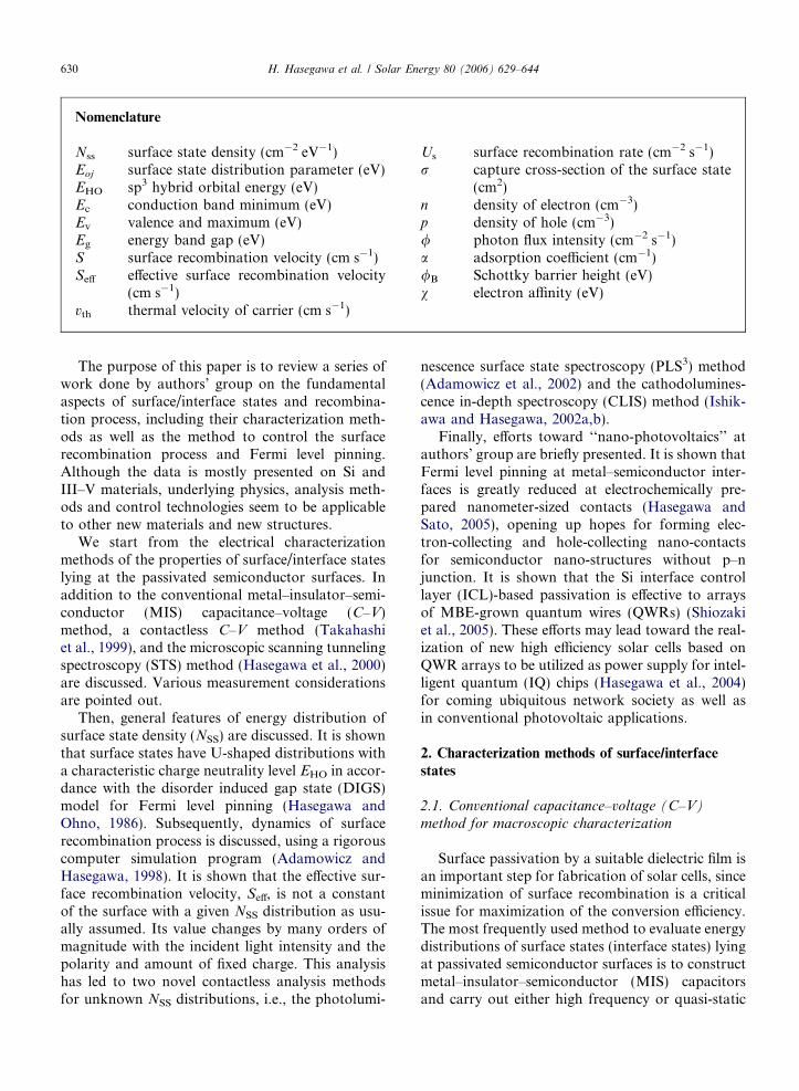
systems. However, difficulties can arise in other MISsystems which exhibit unexpected C–V behavior.An example is given in Fig. 1(a) where anomalousfrequency dispersion behavior of C–V curves gener-ally seen in n-type GaAs MIS capacitors is shownfor a SiN passivated GaAs capacitor. Dependingon how to interpret this dispersion, i.e., whether thisis due to dispersion of permittivity of dielectric ordue to semiconductor surface states, the result ofMIS C–V analysis becomes very different as shownin Fig. 1(b) which is taken from an old paper of ourgroup (Hasegawa and Sawada, 1983). This clearlyillustrates that very careful interpretation and anal-ysis are necessary, when C–V methods are appliedto combinations of new semiconductors and newdielectrics, and some anomalous C–V behavior notdescribed in the textbooks is observed. Anotherpoint is the measurement frequency. In the high fre-quency method, 1 MHz is usually high enough forSi MOS capacitors to obtain their high frequencylimits. However, this may not be the case in otherMIS systems. For example, some III-V MIS capac-itors reached their high frequency limit at GHz fre-quencies (Iizuka et al., 1997) due to very short timeconstants of some parts of surface state continuum.For the quasi static method involving integration ofcharging currents, utmost care has to be made forthe leakage current through the dielectric film.
Gate bias (V)0 10 20
1kHz
10kHz
100kHz
1MHz
GaAs SiNx MIS capacitor
(a)
Fig. 1. (a) Capacitance–voltage anomaly observed in GaAs MIS capacMIS capacitors by various workers.
By a detailed careful C–V study on various GaAsMIS systems, we came to the conclusion that theanomalous frequency dispersion shown inFig. 1(a) is due to high density surface states thathave a specific U-shaped continuous density distri-bution. Namely, the state density has a minimumat about 0.9 eV below the conduction band edgeand sharply increases from near midgap towardsthe conduction band edge.
2.2. Contactless capacitance–voltage (C–V)
method
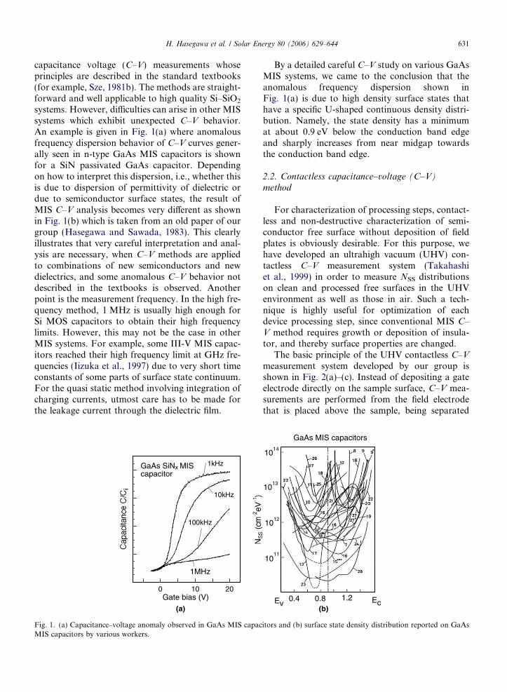
For characterization of processing steps, contact-less and non-destructive characterization of semi-conductor free surface without deposition of fieldplates is obviously desirable. For this purpose, wehave developed an ultrahigh vacuum (UHV) con-tactless C–V measurement system (Takahashiet al., 1999) in order to measure NSS distributionson clean and processed free surfaces in the UHVenvironment as well as those in air. Such a tech-nique is highly useful for optimization of eachdevice processing step, since conventional MIS C–V method requires growth or deposition of insula-tor, and thereby surface properties are changed.
The basic principle of the UHV contactless C–V
measurement system developed by our group isshown in Fig. 2(a)–(c). Instead of depositing a gateelectrode directly on the sample surface, C–V mea-surements are performed from the field electrodethat is placed above the sample, being separated
Ev Ec0.4 0.8 1.2
GaAs MIS capacitors
1014
1013
1012
1011
(b)
itors and (b) surface state density distribution reported on GaAs
sensor head
UHV chamber
connection toother UHVchambers
to vacuum pumps
piezo-unit
sample
anti-vibration mechanism
bottom view of sensor head
parallelismelectrodes
field electrode
UHV gap (Lg)(100-300nm)
side view of sensor head
electrodes evanescent wave
laser diode photo diode
sample
(a)
(b) (c)
Fig. 2. Ultrahigh-vacuum contactless C–V measurement system. (a) Schematic diagram of the system, (b) bottom view of the sensor headand (c) side view of the sensor head.
-0.8-1.2 -0.4 0Ev Ec
Energy (eV)
Nss
(cm
-2eV
-1)
(4x6) (4x6)+1ML Si
(2x4) & c(4x4) (2x4)+1ML Si
c(4x4)+1ML Si
1010
1011
1012
1013
1014
1015
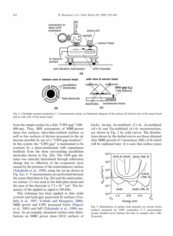
Fig. 3. Distribution of surface state densities on various GaAssurfaces measured by UHV contactless C–V measurementsystem. Dashed curves indicate the data on samples after 1 MLSi growth.
632 H. Hasegawa et al. / Solar Energy 80 (2006) 629–644
from the sample surface by a thin ‘‘UHV-gap’’ (300–400 nm). Thus, MIS assessments of MBE-grownclean free surfaces, ultra-thin-oxidized surfaces aswell as free surfaces of devices processed in the airbecome possible by use of a ‘‘UHV-gap insulator’’.In this system, the ‘‘UHV-gap’’ is maintained to beconstant by a piezo-mechanism with capacitancefeedback from the three surrounding parallelismelectrodes shown in Fig. 2(b). The UHV-gap dis-tance was optically determined through reflectancechange due to reflection of the evanescent wavecaused by the presence of the semiconductor surface(Takahashi et al., 1999), using the set-up shown inFig. 2(c). C–V measurements are performed betweenthe center filed plate in Fig. 2(b) and the semiconduc-tor surface. Cr was used as the field plate metal andthe area of the electrode is 7.5 · 10�3 cm2. The fre-quency of the applied ac signal is 500 kHz.
This technique has been applied to thin oxidecovered and hydrogen passivated Si surfaces (Yos-hida et al., 1997; Yoshida and Hasegawa, 2000),MBE grown and UHV processed GaAs (Negoroet al., 2003) and InP (Takahashi et al., 1999) sur-faces. As an example, measured surface state distri-butions on MBE grown clean (001) surfaces of
GaAs, having As-stabilized (2 · 4), As-stabilizedc(4 · 4) and Ga-stabilized (4 · 6) reconstructions,are shown in Fig. 3 by solid curves. The distribu-tions shown by the dashed curves are those obtainedafter MBE growth of 1 monolayer (ML) of Si whichwill be explained later. It is seen that surface states
H. Hasegawa et al. / Solar Energy 80 (2006) 629–644 633
have roughly U-shaped continuous distributions inboth cases rather than showing well defined discretepeaks. Particularly, surface states on the As-stabi-lized GaAs (2 · 4) surface has a narrow U-shapeddistribution with high densities which will stronglypin the Fermi level at around 0.9 eV below the con-duction band edge. Separate band bending measure-ments by X-ray photoelectron spectroscopy (XPS)technique clearly indicated a very strong Fermi levelpinning. The Ga-stabilized (4 · 6) surface shows awider U-shape, but the distribution sharply risesup at around 0.5 eV below the conduction bandedge. It is interesting to note that the technologicallymost important As-stabilized GaAs (2 · 4) surface,which is usually used as the initial surface for GaAsdevice processing, has the largest surface state den-sity, although the surface shows a well defined andregular (2 · 4) missing dimmer structure under theUHV in situ scanning tunneling microscope. Pres-ence of large band bending on this surface was alsodetected by X-ray photoelectron spectroscopy(XPS) measurements (Ishikawa et al., 1998).
2.3. Scanning tunneling spectroscopy
for microscopic characterization
Recent progress of scanning tunneling micros-copy (STM) has provided very powerful means of
V
gap stateDOS
dIdV
(a)EV EC E
surfacestate
EF(tip)
chaneu
char
(c)
Fig. 4. (a) Usually expected STS spectrum, (b) actually observed STS spgap.
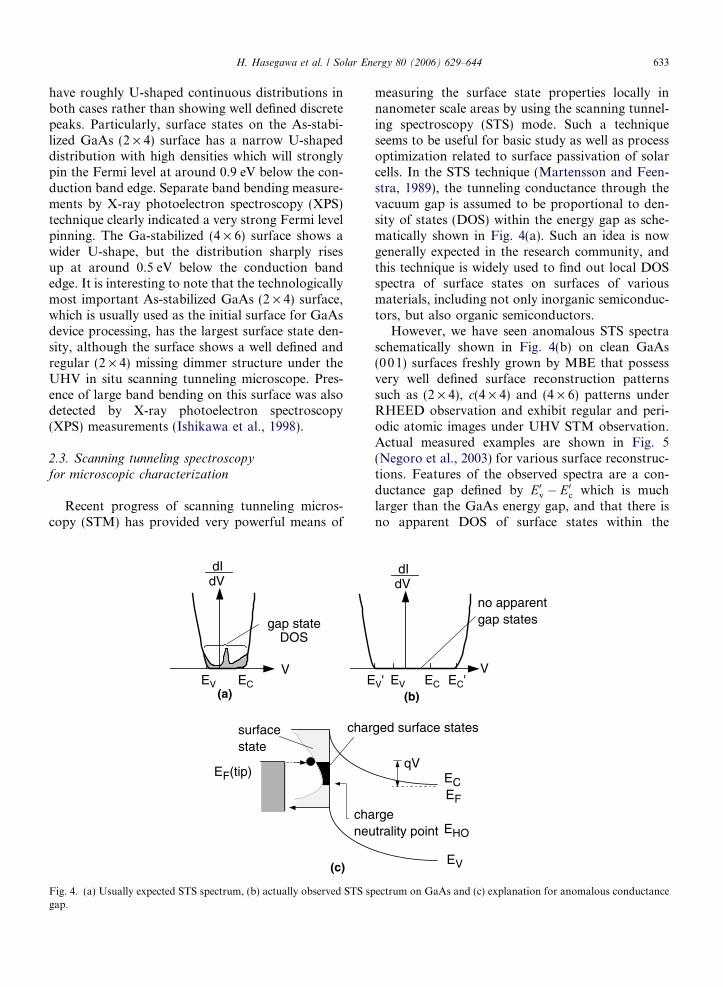
measuring the surface state properties locally innanometer scale areas by using the scanning tunnel-ing spectroscopy (STS) mode. Such a techniqueseems to be useful for basic study as well as processoptimization related to surface passivation of solarcells. In the STS technique (Martensson and Feen-stra, 1989), the tunneling conductance through thevacuum gap is assumed to be proportional to den-sity of states (DOS) within the energy gap as sche-matically shown in Fig. 4(a). Such an idea is nowgenerally expected in the research community, andthis technique is widely used to find out local DOSspectra of surface states on surfaces of variousmaterials, including not only inorganic semiconduc-tors, but also organic semiconductors.
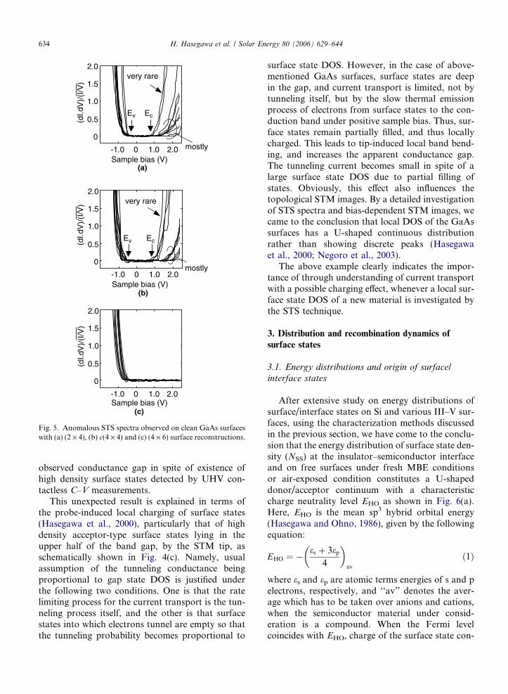
However, we have seen anomalous STS spectraschematically shown in Fig. 4(b) on clean GaAs(001) surfaces freshly grown by MBE that possessvery well defined surface reconstruction patternssuch as (2 · 4), c(4 · 4) and (4 · 6) patterns underRHEED observation and exhibit regular and peri-odic atomic images under UHV STM observation.Actual measured examples are shown in Fig. 5(Negoro et al., 2003) for various surface reconstruc-tions. Features of the observed spectra are a con-ductance gap defined by E0v � E0c which is muchlarger than the GaAs energy gap, and that there isno apparent DOS of surface states within the
V
no apparentgap states
dIdV
EV ECV' EC'(b)
EV
qVECEF
rgetrality point
ged surface states
EHO
ectrum on GaAs and (c) explanation for anomalous conductance
Sample bias (V)0-1.0 1.0 2.0
2.0
1.0
0
1.5
0.5
Sample bias (V)
(dI.d
V)/
(I/V
)
2.0
1.0
0
0-1.0 1.0 2.0
(dI.d
V)/
(I/V
)(d
I.dV
)/(I
/V)
1.5
0.5Ev Ec
very rare
mostly
Sample bias (V)0-1.0 1.0 2.0
2.0
1.0
0
1.5
0.5EcEv
very rare
mostly
(a)
(b)
(c)
Fig. 5. Anomalous STS spectra observed on clean GaAs surfaceswith (a) (2 · 4), (b) c(4 · 4) and (c) (4 · 6) surface reconstructions.
634 H. Hasegawa et al. / Solar Energy 80 (2006) 629–644
observed conductance gap in spite of existence ofhigh density surface states detected by UHV con-tactless C–V measurements.
This unexpected result is explained in terms ofthe probe-induced local charging of surface states(Hasegawa et al., 2000), particularly that of highdensity acceptor-type surface states lying in theupper half of the band gap, by the STM tip, asschematically shown in Fig. 4(c). Namely, usualassumption of the tunneling conductance beingproportional to gap state DOS is justified underthe following two conditions. One is that the ratelimiting process for the current transport is the tun-neling process itself, and the other is that surfacestates into which electrons tunnel are empty so thatthe tunneling probability becomes proportional to
surface state DOS. However, in the case of above-mentioned GaAs surfaces, surface states are deepin the gap, and current transport is limited, not bytunneling itself, but by the slow thermal emissionprocess of electrons from surface states to the con-duction band under positive sample bias. Thus, sur-face states remain partially filled, and thus locallycharged. This leads to tip-induced local band bend-ing, and increases the apparent conductance gap.The tunneling current becomes small in spite of alarge surface state DOS due to partial filling ofstates. Obviously, this effect also influences thetopological STM images. By a detailed investigationof STS spectra and bias-dependent STM images, wecame to the conclusion that local DOS of the GaAssurfaces has a U-shaped continuous distributionrather than showing discrete peaks (Hasegawaet al., 2000; Negoro et al., 2003).
The above example clearly indicates the impor-tance of through understanding of current transportwith a possible charging effect, whenever a local sur-face state DOS of a new material is investigated bythe STS technique.
3. Distribution and recombination dynamics of
surface states
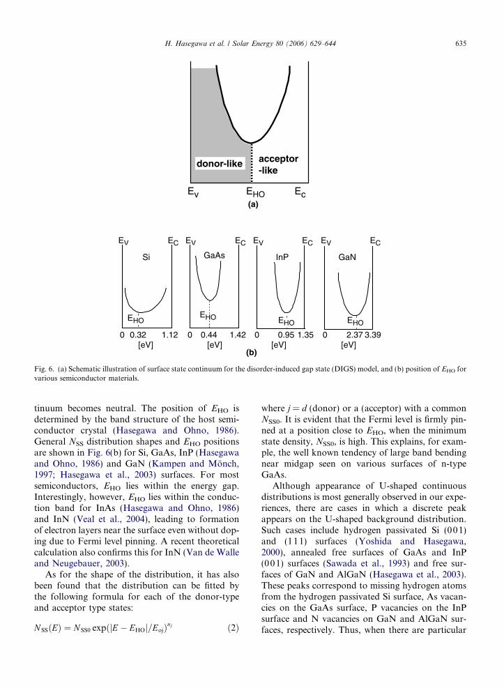
3.1. Energy distributions and origin of surface/interface states
After extensive study on energy distributions ofsurface/interface states on Si and various III–V sur-faces, using the characterization methods discussedin the previous section, we have come to the conclu-sion that the energy distribution of surface state den-sity (NSS) at the insulator–semiconductor interfaceand on free surfaces under fresh MBE conditionsor air-exposed condition constitutes a U-shapeddonor/acceptor continuum with a characteristiccharge neutrality level EHO as shown in Fig. 6(a).Here, EHO is the mean sp3 hybrid orbital energy(Hasegawa and Ohno, 1986), given by the followingequation:
EHO ¼ �es þ 3ep
4
� �av
ð1Þ
where es and ep are atomic terms energies of s and pelectrons, respectively, and ‘‘av’’ denotes the aver-age which has to be taken over anions and cations,when the semiconductor material under consid-eration is a compound. When the Fermi levelcoincides with EHO, charge of the surface state con-
Ev EcEHO
donor-like acceptor-like
(a)
(b)
EV EC
Si
0 0.32
EHO
1.12[eV]
EV EC
0 0.44
EHO
1.42[eV]
EV EC
InP
0 0.95
EHO
1.35[eV]
EV EC
GaN
0 2.37
EHO
[eV]3.39
GaAs
Fig. 6. (a) Schematic illustration of surface state continuum for the disorder-induced gap state (DIGS) model, and (b) position of EHO forvarious semiconductor materials.
H. Hasegawa et al. / Solar Energy 80 (2006) 629–644 635
tinuum becomes neutral. The position of EHO isdetermined by the band structure of the host semi-conductor crystal (Hasegawa and Ohno, 1986).General NSS distribution shapes and EHO positionsare shown in Fig. 6(b) for Si, GaAs, InP (Hasegawaand Ohno, 1986) and GaN (Kampen and Monch,1997; Hasegawa et al., 2003) surfaces. For mostsemiconductors, EHO lies within the energy gap.Interestingly, however, EHO lies within the conduc-tion band for InAs (Hasegawa and Ohno, 1986)and InN (Veal et al., 2004), leading to formationof electron layers near the surface even without dop-ing due to Fermi level pinning. A recent theoreticalcalculation also confirms this for InN (Van de Walleand Neugebauer, 2003).
As for the shape of the distribution, it has alsobeen found that the distribution can be fitted bythe following formula for each of the donor-typeand acceptor type states:
NSSðEÞ ¼ N SS0 expðjE � EHOj=EojÞnj ð2Þ
where j = d (donor) or a (acceptor) with a commonNSS0. It is evident that the Fermi level is firmly pin-ned at a position close to EHO, when the minimumstate density, NSS0, is high. This explains, for exam-ple, the well known tendency of large band bendingnear midgap seen on various surfaces of n-typeGaAs.
Although appearance of U-shaped continuousdistributions is most generally observed in our expe-riences, there are cases in which a discrete peakappears on the U-shaped background distribution.Such cases include hydrogen passivated Si (001)and (111) surfaces (Yoshida and Hasegawa,2000), annealed free surfaces of GaAs and InP(001) surfaces (Sawada et al., 1993) and free sur-faces of GaN and AlGaN (Hasegawa et al., 2003).These peaks correspond to missing hydrogen atomsfrom the hydrogen passivated Si surface, As vacan-cies on the GaAs surface, P vacancies on the InPsurface and N vacancies on GaN and AlGaN sur-faces, respectively. Thus, when there are particular

636 H. Hasegawa et al. / Solar Energy 80 (2006) 629–644
types of dominant defects that are produced orremaining on the surface after insulator formation,processing or annealing, they appear as discretepeaks on the U-shaped background distribution.Appearance of discrete peaks were also reportedon ultrathin oxide covered Si surfaces by otherworkers (Kobayashi et al., 1996; Yamashita et al.,1996), using an XPS-based new technique.
Obviously, understanding the origin of surfacestates and related Fermi level pinning is an impor-tant issue for the progress of the surface passivationand other surface/interface related science and tech-nology. One remarkable feature related to this issueis that there is a strong correlation between theenergy position of Fermi level pinning on variousfree surfaces and insulator–semiconductor (I–S)interfaces and those at the metal–semiconductor(M–S) surfaces (Hasegawa and Ohno, 1986; Adam-owicz et al., 2002), both being very close to the posi-tion of EHO. In order to explain this correlation, theunified defect model (UDM) (Spicer et al., 1980)and the disorder induced gap state (DIGS) modelwere proposed, as summarized in Table 1. The for-mer ascribes the origin of the surface states to stoi-chiometry-related defects at the surface where the
Table 1Major models for Fermi level pinning at semiconductor surfaces and i
Model Origin of pinning Nss distribution andpinning position
Unified defect model Deep level relatedto stoichiometry,especially, AsGa
DIGS model Loss of 2D periodicitydue to disorder ofbonds at interface
mean hybridorbital energy
MIGS model Penetration of metalwave function intosemiconductor
midgap energy
V–S: Vacuum–semiconductor interface; S–S: semiconductor–semiconmetal–semiconductor interface.
Fermi level is pinned near the peak of the discreteDOS. On the other hand, the latter explains the ori-gin in terms of loss of two-dimensional periodicityof the host crystal at the surface caused by bond dis-order, producing a U-shaped donor/acceptor con-tinuum where the Fermi level is pinned near thecharge neutrality level, EHO. There is also a modelcalled metal-induced gap state (MIGS) model(Heine, 1965; Tersoff, 1984) which is solely applica-ble to the metal–semiconductor interface. Accord-ing to this model, evanescent tails of metalwavefunctions produce a donor/accepter gap statecontinuum with a charge neutrality level EHO whichpins the Fermi level at EHO. This model cannotexplain the above-mentioned correlation of the pin-ning position between I–S and M–S interfaces.
The above-mentioned appearance of peaks onthe U-shaped background in some surfaces as men-tioned above, indicates that both situations assumedin the UDM and DIGS models can take place.However our wide range of experiments have indi-cated that the pinning position is near to EHO evenwhen defect DOS peaks are observable. Our inter-pretation is that there is a strong tendency to avoidgeneration of energetically unfavorable isolated
nterfaces
Applicableinterfaces
Nature ofpinning
References
V–S, S–S,I–S, M–S
Extrinsic Spicer et al. (1980)
V–S, S–S,I–S, M–S
Extrinsic Hasegawa and Ohno (1986)
M–S Intrinsic (Heine, 1965; Tersoff, 1984)
ductor interface; I–S: insulator–semiconductor interface; M–S:
H. Hasegawa et al. / Solar Energy 80 (2006) 629–644 637
defects on the surface by screening these defects bysmall amount of bond disorder of host atoms. Sucha tendency was clearly observed by detailed study ofGaAs clean surface using STM (Negoro et al., 2003;Hasegawa et al., 2000).
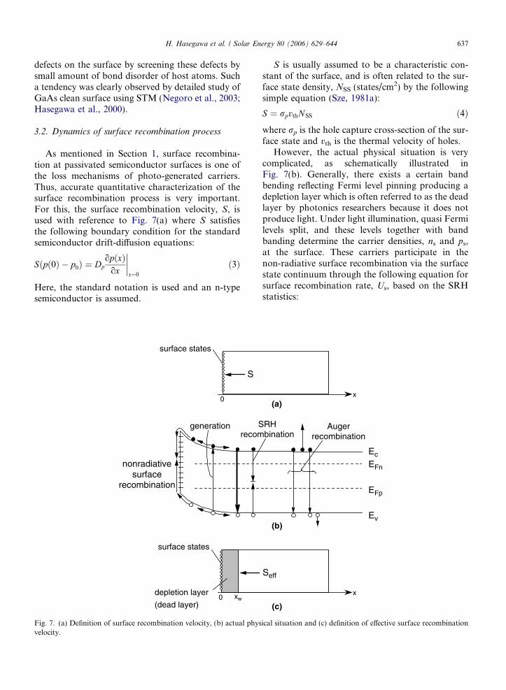
3.2. Dynamics of surface recombination process
As mentioned in Section 1, surface recombina-tion at passivated semiconductor surfaces is one ofthe loss mechanisms of photo-generated carriers.Thus, accurate quantitative characterization of thesurface recombination process is very important.For this, the surface recombination velocity, S, isused with reference to Fig. 7(a) where S satisfiesthe following boundary condition for the standardsemiconductor drift-diffusion equations:
Sðpð0Þ � p0Þ ¼ DpopðxÞox
����x¼0
ð3Þ
Here, the standard notation is used and an n-typesemiconductor is assumed.
nonradiativesurface
recombination
Srecom
generation
surface states
depletion layer
(dead layer)xw0
0
S
surface states
Fig. 7. (a) Definition of surface recombination velocity, (b) actual physvelocity.
S is usually assumed to be a characteristic con-stant of the surface, and is often related to the sur-face state density, NSS (states/cm2) by the followingsimple equation (Sze, 1981a):
S ¼ rpvthNSS ð4Þwhere rp is the hole capture cross-section of the sur-face state and vth is the thermal velocity of holes.
However, the actual physical situation is verycomplicated, as schematically illustrated inFig. 7(b). Generally, there exists a certain bandbending reflecting Fermi level pinning producing adepletion layer which is often referred to as the deadlayer by photonics researchers because it does notproduce light. Under light illumination, quasi Fermilevels split, and these levels together with bandbanding determine the carrier densities, ns and ps,at the surface. These carriers participate in thenon-radiative surface recombination via the surfacestate continuum through the following equation forsurface recombination rate, Us, based on the SRHstatistics:
Augerrecombination
RHbination
EFn
EFp
Ec
Ev(b)
(c)
Seff
x
x(a)
ical situation and (c) definition of effective surface recombination
(a)
(b)
106
105
104
103
102
101
108 1012 1016 1020 1024
107
106
105
104
103
102
Photon flux density (cm-2s-1)
Photon flux density (cm
Sef
f (cm
/s)
Sef
f (cm
/s)
-2s-1)
109 1012 1015 1018 10241021
-8x10¹⁰depletion
-2x10¹⁰
-1x10¹¹
0
2x10¹⁰
-2x10¹¹
QFC=1x1011cm-2
inversion
accumulation
-5x10¹⁰
EV ECEHO
1012
1011
(cm-2eV-1) Nss(E)
n-Si
EV ECEHO
1012
(cm-2eV-1) Nss(E)
1013
1014
n-GaAs
depletion
inversion accumulation
QFC=0 cm-2
1x10¹³
5x10¹³
1.5x10¹⁴
-5x10¹¹
-7x10¹¹ 2x10¹⁴
Fig. 8. Plots of calculated effective surface recombination veloc-ity vs. photon flux density for (a) n-Si and (b) n-GaAs.
638 H. Hasegawa et al. / Solar Energy 80 (2006) 629–644
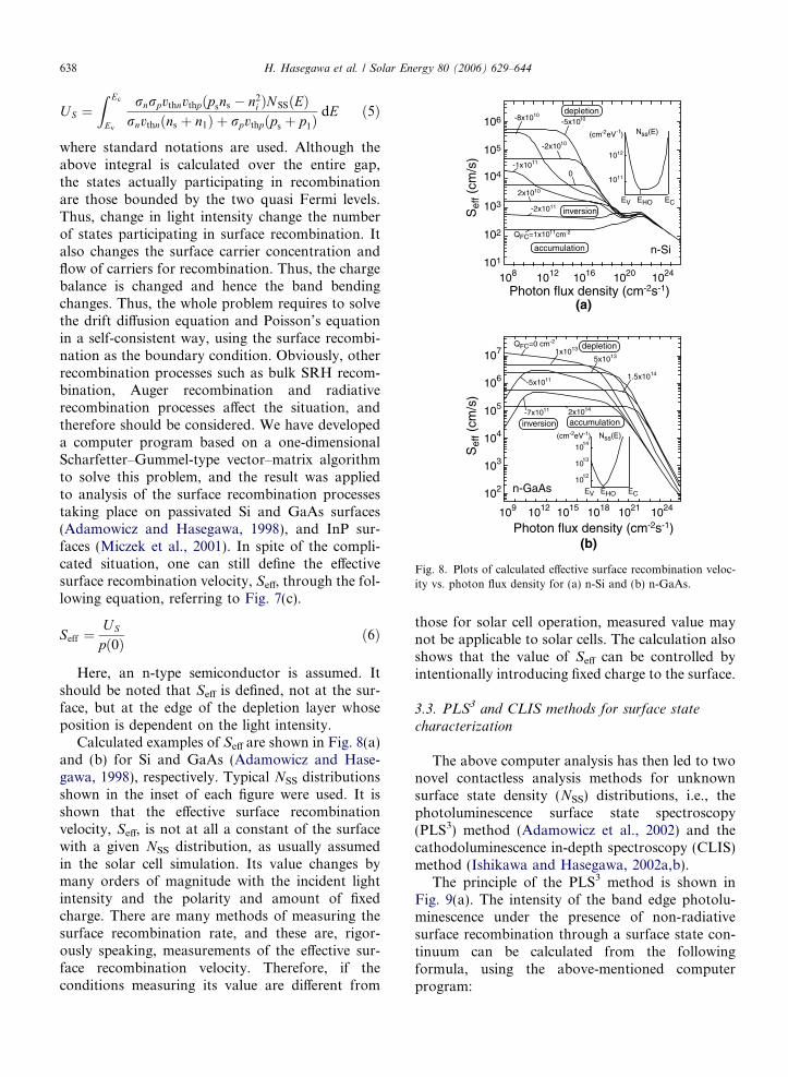
US ¼Z Ec
Ev
rnrpvthnvthpðpsns � n2i ÞN SSðEÞ
rnvthnðns þ n1Þ þ rpvthpðps þ p1ÞdE ð5Þ
where standard notations are used. Although theabove integral is calculated over the entire gap,the states actually participating in recombinationare those bounded by the two quasi Fermi levels.Thus, change in light intensity change the numberof states participating in surface recombination. Italso changes the surface carrier concentration andflow of carriers for recombination. Thus, the chargebalance is changed and hence the band bendingchanges. Thus, the whole problem requires to solvethe drift diffusion equation and Poisson’s equationin a self-consistent way, using the surface recombi-nation as the boundary condition. Obviously, otherrecombination processes such as bulk SRH recom-bination, Auger recombination and radiativerecombination processes affect the situation, andtherefore should be considered. We have developeda computer program based on a one-dimensionalScharfetter–Gummel-type vector–matrix algorithmto solve this problem, and the result was appliedto analysis of the surface recombination processestaking place on passivated Si and GaAs surfaces(Adamowicz and Hasegawa, 1998), and InP sur-faces (Miczek et al., 2001). In spite of the compli-cated situation, one can still define the effectivesurface recombination velocity, Seff, through the fol-lowing equation, referring to Fig. 7(c).
Seff ¼U S
pð0Þ ð6Þ
Here, an n-type semiconductor is assumed. Itshould be noted that Seff is defined, not at the sur-face, but at the edge of the depletion layer whoseposition is dependent on the light intensity.
Calculated examples of Seff are shown in Fig. 8(a)and (b) for Si and GaAs (Adamowicz and Hase-gawa, 1998), respectively. Typical NSS distributionsshown in the inset of each figure were used. It isshown that the effective surface recombinationvelocity, Seff, is not at all a constant of the surfacewith a given NSS distribution, as usually assumedin the solar cell simulation. Its value changes bymany orders of magnitude with the incident lightintensity and the polarity and amount of fixedcharge. There are many methods of measuring thesurface recombination rate, and these are, rigor-ously speaking, measurements of the effective sur-face recombination velocity. Therefore, if theconditions measuring its value are different from
those for solar cell operation, measured value maynot be applicable to solar cells. The calculation alsoshows that the value of Seff can be controlled byintentionally introducing fixed charge to the surface.
3.3. PLS3 and CLIS methods for surface state
characterization
The above computer analysis has then led to twonovel contactless analysis methods for unknownsurface state density (NSS) distributions, i.e., thephotoluminescence surface state spectroscopy(PLS3) method (Adamowicz et al., 2002) and thecathodoluminescence in-depth spectroscopy (CLIS)method (Ishikawa and Hasegawa, 2002a,b).
The principle of the PLS3 method is shown inFig. 9(a). The intensity of the band edge photolu-minescence under the presence of non-radiativesurface recombination through a surface state con-tinuum can be calculated from the followingformula, using the above-mentioned computerprogram:
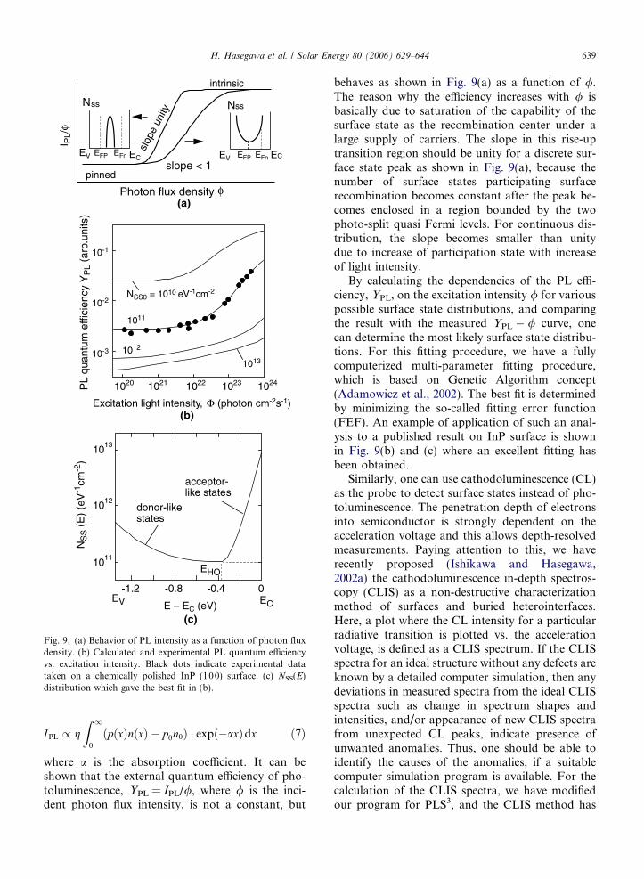
slope < 1
Nss
Photon flux density
intrinsic
pinned
EV EC
Nss
EV ECEFP EFn EFP EFn
(a)
(b)
(c)
1020 1021 1022 1023 1024
Excitation light intensity, (photon cm-2s-1)
10-1
10-2
10-3
NSS0 = 1010 eV-1cm-2
1011
1012
1013
1013
1012
1011
donor-likestates
acceptor-like states
-1.2 -0.8
E – EC (eV)
EHO
ECEV-0.4 0
PL
quan
tum
effi
cien
cy Y
PL
(arb
.uni
ts)
NS
S (
E)
(eV
-1cm
-2)
slop
e un
ity
Fig. 9. (a) Behavior of PL intensity as a function of photon fluxdensity. (b) Calculated and experimental PL quantum efficiencyvs. excitation intensity. Black dots indicate experimental datataken on a chemically polished InP (100) surface. (c) NSS(E)distribution which gave the best fit in (b).
H. Hasegawa et al. / Solar Energy 80 (2006) 629–644 639
IPL / gZ 1
0
ðpðxÞnðxÞ � p0n0Þ � expð�axÞdx ð7Þ
where a is the absorption coefficient. It can beshown that the external quantum efficiency of pho-toluminescence, YPL = IPL//, where / is the inci-dent photon flux intensity, is not a constant, but
behaves as shown in Fig. 9(a) as a function of /.The reason why the efficiency increases with / isbasically due to saturation of the capability of thesurface state as the recombination center under alarge supply of carriers. The slope in this rise-uptransition region should be unity for a discrete sur-face state peak as shown in Fig. 9(a), because thenumber of surface states participating surfacerecombination becomes constant after the peak be-comes enclosed in a region bounded by the twophoto-split quasi Fermi levels. For continuous dis-tribution, the slope becomes smaller than unitydue to increase of participation state with increaseof light intensity.
By calculating the dependencies of the PL effi-ciency, YPL, on the excitation intensity / for variouspossible surface state distributions, and comparingthe result with the measured YPL � / curve, onecan determine the most likely surface state distribu-tions. For this fitting procedure, we have a fullycomputerized multi-parameter fitting procedure,which is based on Genetic Algorithm concept(Adamowicz et al., 2002). The best fit is determinedby minimizing the so-called fitting error function(FEF). An example of application of such an anal-ysis to a published result on InP surface is shownin Fig. 9(b) and (c) where an excellent fitting hasbeen obtained.
Similarly, one can use cathodoluminescence (CL)as the probe to detect surface states instead of pho-toluminescence. The penetration depth of electronsinto semiconductor is strongly dependent on theacceleration voltage and this allows depth-resolvedmeasurements. Paying attention to this, we haverecently proposed (Ishikawa and Hasegawa,2002a) the cathodoluminescence in-depth spectros-copy (CLIS) as a non-destructive characterizationmethod of surfaces and buried heterointerfaces.Here, a plot where the CL intensity for a particularradiative transition is plotted vs. the accelerationvoltage, is defined as a CLIS spectrum. If the CLISspectra for an ideal structure without any defects areknown by a detailed computer simulation, then anydeviations in measured spectra from the ideal CLISspectra such as change in spectrum shapes andintensities, and/or appearance of new CLIS spectrafrom unexpected CL peaks, indicate presence ofunwanted anomalies. Thus, one should be able toidentify the causes of the anomalies, if a suitablecomputer simulation program is available. For thecalculation of the CLIS spectra, we have modifiedour program for PLS3, and the CLIS method has
640 H. Hasegawa et al. / Solar Energy 80 (2006) 629–644
been successfully applied to various heterostruc-tures. It was found that it is vitally necessary toinclude surface recombination in the calculation inorder to reproduce the experimental spectra. Forthis, we included SRH recombination through aU-shaped surface state continuum similarly to thecase of the PLS3 method (Ishikawa and Hasegawa,2002b). Thus, the method can be used for the sur-face state analysis.
4. Controls of surface states in nano-structures
toward nano-photovoltaics
4.1. IQ-chip and nano-photovoltaics
Recent rapid progress of nanotechnology hascreated interest in the photovoltaic area, as alreadymentioned previously. According to literature (Cor-kish et al., 2002), advantages expected in solar cellsutilizing nano-structures is reduction of amount ofmaterials, increased light absorption, higher effi-ciency, improvement of spatial uniformity, reducedcontact area, tunability of effective band gap dueto quantum confinement etc. These features maybe combined to produce high efficiency cells withlower cost as the next generation, clean and renew-able energy sources.
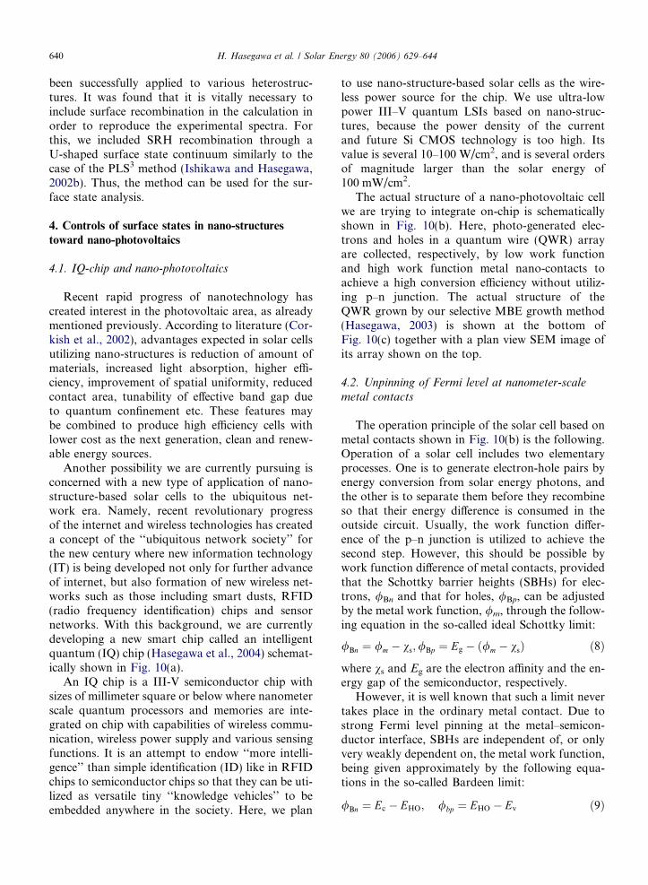
Another possibility we are currently pursuing isconcerned with a new type of application of nano-structure-based solar cells to the ubiquitous net-work era. Namely, recent revolutionary progressof the internet and wireless technologies has createda concept of the ‘‘ubiquitous network society’’ forthe new century where new information technology(IT) is being developed not only for further advanceof internet, but also formation of new wireless net-works such as those including smart dusts, RFID(radio frequency identification) chips and sensornetworks. With this background, we are currentlydeveloping a new smart chip called an intelligentquantum (IQ) chip (Hasegawa et al., 2004) schemat-ically shown in Fig. 10(a).
An IQ chip is a III-V semiconductor chip withsizes of millimeter square or below where nanometerscale quantum processors and memories are inte-grated on chip with capabilities of wireless commu-nication, wireless power supply and various sensingfunctions. It is an attempt to endow ‘‘more intelli-gence’’ than simple identification (ID) like in RFIDchips to semiconductor chips so that they can be uti-lized as versatile tiny ‘‘knowledge vehicles’’ to beembedded anywhere in the society. Here, we plan
to use nano-structure-based solar cells as the wire-less power source for the chip. We use ultra-lowpower III–V quantum LSIs based on nano-struc-tures, because the power density of the currentand future Si CMOS technology is too high. Itsvalue is several 10–100 W/cm2, and is several ordersof magnitude larger than the solar energy of100 mW/cm2.
The actual structure of a nano-photovoltaic cellwe are trying to integrate on-chip is schematicallyshown in Fig. 10(b). Here, photo-generated elec-trons and holes in a quantum wire (QWR) arrayare collected, respectively, by low work functionand high work function metal nano-contacts toachieve a high conversion efficiency without utiliz-ing p–n junction. The actual structure of theQWR grown by our selective MBE growth method(Hasegawa, 2003) is shown at the bottom ofFig. 10(c) together with a plan view SEM image ofits array shown on the top.
4.2. Unpinning of Fermi level at nanometer-scale
metal contacts
The operation principle of the solar cell based onmetal contacts shown in Fig. 10(b) is the following.Operation of a solar cell includes two elementaryprocesses. One is to generate electron-hole pairs byenergy conversion from solar energy photons, andthe other is to separate them before they recombineso that their energy difference is consumed in theoutside circuit. Usually, the work function differ-ence of the p–n junction is utilized to achieve thesecond step. However, this should be possible bywork function difference of metal contacts, providedthat the Schottky barrier heights (SBHs) for elec-trons, /Bn and that for holes, /Bp, can be adjustedby the metal work function, /m, through the follow-ing equation in the so-called ideal Schottky limit:
/Bn ¼ /m � vs;/Bp ¼ Eg � ð/m � vsÞ ð8Þ
where vs and Eg are the electron affinity and the en-ergy gap of the semiconductor, respectively.
However, it is well known that such a limit nevertakes place in the ordinary metal contact. Due tostrong Fermi level pinning at the metal–semicon-ductor interface, SBHs are independent of, or onlyvery weakly dependent on, the metal work function,being given approximately by the following equa-tions in the so-called Bardeen limit:
/Bn ¼ Ec � EHO; /bp ¼ EHO � Ev ð9Þ
3 m
GaAs QWR arrays on (001)
planview
bottom QW (001) GaAs sub.
GaAs QWR
side QW
<110>
GaAsbuffer
AlGaAs
(c)
low workfunctionmetal nano-contacts
QWR array
high workfunctionmetal nano-contacts
vertical stacking ofQWRs with different wire dimensions
(b)
rectenna,solar cell
communi-cationcircuits
sensors
CPU,memory
microwavemillimeter waveTHzlight
sun lightroom light
Wireless communicationcircuit
a few 100-1,000 µm
Ultra-low powerIII-V quantum LSIs
(nanoprocessor, nanomemory)
Power supplyUltra-high sensitive sensor
utilizing nanostructures
(a)
nano-photovoltaics
Fig. 10. (a) Concepts of the IQ chip, (b) nano-photovoltaic device based on a quantum wire (QWR) array and metal nano-contacts. (c)QWR structure and a plan view SEM image. QWR arrays are fabricated by the selective MBE growth method.
H. Hasegawa et al. / Solar Energy 80 (2006) 629–644 641
From the viewpoint of the MIGS model in Table 1,the Fermi pinning is an intrinsic one caused by themetal wavefunction tail, and SBHs can not be chan-ged by the metal work function.
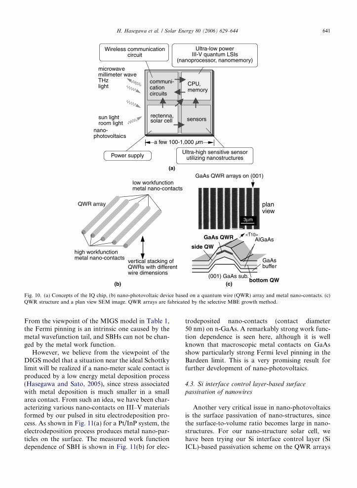
However, we believe from the viewpoint of theDIGS model that a situation near the ideal Schottkylimit will be realized if a nano-meter scale contact isproduced by a low energy metal deposition process(Hasegawa and Sato, 2005), since stress associatedwith metal deposition is much smaller in a smallarea contact. From such an idea, we have been char-acterizing various nano-contacts on III–V materialsformed by our pulsed in situ electrodeposition pro-cess. As shown in Fig. 11(a) for a Pt/InP system, theelectrodeposition process produces metal nano-par-ticles on the surface. The measured work functiondependence of SBH is shown in Fig. 11(b) for elec-
trodeposited nano-contacts (contact diameter50 nm) on n-GaAs. A remarkably strong work func-tion dependence is seen here, although it is wellknown that macroscopic metal contacts on GaAsshow particularly strong Fermi level pinning in theBardeen limit. This is a very promising result forfurther development of nano-photovoltaics.
4.3. Si interface control layer-based surface
passivation of nanowires
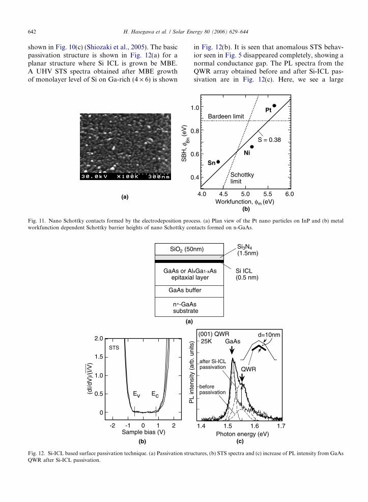
Another very critical issue in nano-photovoltaicsis the surface passivation of nano-structures, sincethe surface-to-volume ratio becomes large in nano-structures. For our nano-structure solar cell, wehave been trying our Si interface control layer (SiICL)-based passivation scheme on the QWR arrays
642 H. Hasegawa et al. / Solar Energy 80 (2006) 629–644
shown in Fig. 10(c) (Shiozaki et al., 2005). The basicpassivation structure is shown in Fig. 12(a) for aplanar structure where Si ICL is grown be MBE.A UHV STS spectra obtained after MBE growthof monolayer level of Si on Ga-rich (4 · 6) is shown
(a)
1
0
0
0B
nS
BH
, (e
V)
φ
Fig. 11. Nano Schottky contacts formed by the electrodeposition procworkfunction dependent Schottky barrier heights of nano Schottky co
SiO2 (50
GaAs or Aepitaxia
GaAs bu
n+-GaAsubstra
(a)
Sample bias (V)0 1 2-1-2
0.5
1.0
1.5
2.0
0
Ev Ec
(b)
(dI/d
V)/
(I/V
)
STS
Fig. 12. Si-ICL based surface passivation technique. (a) Passivation struQWR after Si-ICL passivation.
in Fig. 12(b). It is seen that anomalous STS behav-ior seen in Fig. 5 disappeared completely, showing anormal conductance gap. The PL spectra from theQWR array obtained before and after Si-ICL pas-sivation are in Fig. 12(c). Here, we see a large
Workfunction, φm (eV)4.0 4.5 5.0 5.5 6.0
.0
.8
.6
.4
Sn
Ni
PtBardeen limit
Schottkylimit
S = 0.38
(b)
ess. (a) Plan view of the Pt nano particles on InP and (b) metalntacts formed on n-GaAs.
nm)
lxGa1-xAsl layer
ffer
ste
Si3N4(1.5nm)
Si ICL(0.5 nm)
1.4 1.5 1.6 1.7Photon energy (eV)
PL
inte
nsity
(ar
b. u
nits
) GaAs
QWRafter Si-ICL passivation
beforepassivation
d=10nm25K
(001) QWR
(c)
ctures, (b) STS spectra and (c) increase of PL intensity from GaAs

H. Hasegawa et al. / Solar Energy 80 (2006) 629–644 643
increase of PL intensity, indicating successful pas-sivation. According to a theoretical analysis, surfacerecombination caused by carrier tunneling fromQWR region is almost completely suppressed dueto removal of surface states.
5. Summary
In this paper, a series of our work on character-ization methods and fundamental aspects of sur-face/interface states and recombination process inSi and III–V materials are reviewed.
In addition to the conventional metal–insulator–semiconductor (MIS) capacitance–voltage (C–V)method, a contactless C–V method and the micro-scopic scanning tunneling spectroscopy (STS)method are discussed, and advantages and measure-ment pitfalls are pointed out.
Then, general features of surface states are dis-cussed. Surface states are shown to have U-shapeddistributions of donor–acceptor continuum with acharacteristic charge neutrality level EHO. Rigoroussimulation of dynamics of surface recombinationprocess has shown that the effective surface recom-bination velocity, Seff, is not a constant of the sur-face but its value changes by many orders ofmagnitude with the incident light intensity and thepolarity and amount of fixed charge. This led totwo related characterization techniques called thephotoluminescence surface state spectroscopy(PLS3) and the cathodoluminescence in-depth spec-troscopy (CLIS).
Finally, attempts to control surface states andFermi level at metal semiconductor interface andfree surfaces of nano-structures were presented, giv-ing promising results and hope for future ‘‘nano-photovoltaics’’.
Acknowledgements
This work is supported by a 21st Century COE(Center of Excellence) program at Hokkaido Uni-versity on ‘‘Meme-media technology approach tothe R&D of next generation ITs’’ from MEXT,Japan.
References
Adamowicz, B., Hasegawa, H., 1998. Computer analysis ofsurface recombination process at Si and compound semicon-ductor surfaces and behavior of surface recombinationvelocity. Jpn. J. Appl. Phys. 37, 1631–1637.
Adamowicz, B., Miczek, M., Arabasz, S., Hasegawa, H., 2002.Rigorous analysis of photoluminescence efficiency for char-acterization of electronic properties of InP(001) surfaces.Vacuum 67, 3–10.
Corkish, R., Kettemann, S., Nelson, J., (Guest Editors), 2002. seepapers in special issue of Physica E 14, issue 1–2 on‘‘Nanostructures on Photovoltaics’’.
Hasegawa, H., 2003. Formation of III–V low dimensionalstructures and their applications to intelligent quantum chips.Microelectronics Journal 34, 341–345.
Hasegawa, H., Sawada, T., 1983. On the electrical properties ofcompound semiconductor interfaces in metal/insulator/semi-conductor structures and the possible origin of interfacestates. Thin Solid Films 103, 119–140.
Hasegawa, H., Ohno, H., 1986. Unified disorder induced gapstate model for insulator–semiconductor and metal–semicon-ductor interfaces. J. Vac. Sci. Technol. B 4, 1130–1138.
Hasegawa, H., Negoro, N., Kasai, S., Ishikawa, Y., Fujikura, H.,2000. Effects of gap states on scanning tunneling spectraobserved on (110)- and (001)-oriented clean surfaces andultrathin Si layer covered surfaces of GaAs prepared bymolecular beam epitaxy. J. Vac. Sci. Technol. B 18, 2100–2108.
Hasegawa, H., Inagaki, T., Ootomo, S., Hashizume, T., 2003.Mechanism of current collapse and gate leakage currents inAlGaN/GaN heterostructure field effect transistors. J. Vac.Sci. Technol. B 21, 1844–1855.
Hasegawa, H., Kasai, S., Sato, T., 2004. Hexagonal binarydecision diagram quantum circuit approach for ultra-lowpower III–V quantum LSIs. IEICE Trans. Electron. E87-C,1757–1768.
Hasegawa, H., Sato, T., 2005. Electrochemical processes forformation, processing and gate control of III–V semiconduc-tor nanostructures. Electrochimica Acta 50, 3015–3027.
Heine, V., 1965. Theory of surface states. Phys. Rev. 138, 1689–1696.
Iizuka, K., Hashizume, T., Hasegawa, H., 1997. Small-signalresponse of interface states at passive InGaAs surfaces fromlow frequencies up to microwave frequencies. Solid StateElectron. 41, 1463–1468.
Ishikawa, F., Hasegawa, H., 2002a. Depth-resolved cathodolu-minescence characterization of buried InGaP/GaP heteroin-terfaces. Appl. Surf. Sci. 190, 508–512.
Ishikawa, F., Hasegawa, H., 2002b. Self-consistent computeranalysis of cathodoluminescence in-depth spectra for com-pound semiconductor heterostructures. Inst. Phys. Conf. Ser.170, 461–466.
Ishikawa, Y., Tsurumi, N., Fukui, T., Hasegawa, H., 1998.Scanning tunneling microscopy and X-ray photoelectronspectroscopy studies of atomic level structure and FermiLevel pinning on GaAs (110) surfaces grown by molecularbeam epitaxy. J. Vac. Sci. Technol. B 16, 2387–2394.
Kampen, T.U., Monch, W., 1997. Barrier heights of GaNSchottky contacts. Appl. Surf. Sci. 117/118, 388–393.
Kobayashi, H., Yamashita, Y., Nakato, Y., Komeda, T.,Nishioka, Y., 1996. Interface states at ultrathin oxide/Si(111) interfaces obtained from X-ray photoelectron spec-troscopy measurements under biases. Appl. Phys. Lett. 69,2276–2278.
Martensson, P., Feenstra, R.M., 1989. Geometric and electronicstructure of antimony on the GaAs (110) surface studied byscanning tunneling microscopy. Phys. Rev. B 39, 7744–7753.
644 H. Hasegawa et al. / Solar Energy 80 (2006) 629–644
Miczek, M., Adamowicz, B., Szuber, J., Hasegawa, H., 2001.Computer analysis of photoluminescence efficiency at InPsurface with U-shaped surface state continuum. Vacuum 63,223–227.
Negoro, N., Anantathanasarn, S., Hasegawa, H., 2003. Effects ofSi deposition on the properties of Ga-rich (4 · 6) GaAs (001)surfaces. J. Vac. Sci. Technol. B 21, 1945–1952.
Sawada, T., Numata, K., Tohdoh, S., Saitoh, T., Hasegawa, H.,1993. In-situ characterization of compound semiconductorsurfaces by novel photoluminescence surface state spectros-copy. Jpn. J. Appl. Phys. 32, 511–517.
Shiozaki, N., Sato, T., Hasegawa, H., 2005. Effects of surfacestates and Si-interlayer based surface passivation on GaAsquantum wires grown by selective molecular beam epitaxy. J.Vac. Sci. Technol. B 23, 1714–1721.
Spicer, W.E., Lindau, I., Skeath, P.R., Su, C.Y., 1980. Unifieddefect model and beyond. J. Vac. Sci. Technol. 17, 1019–1027.
Sze, S.M., 1981a. Physics of Semiconductor Devices, second ed.John Wiley & Sons, New York, pp. 7–60, Chapter 1.
Sze, S.M., 1981b. Physics of Semiconductor Devices, second ed.John Wiley & Sons, New York, pp. 362–430, Chapter 7.
Takahashi, H., Hashizume, T., Hasegawa, H., 1999. X-rayphotoelectron spectroscopy and ultrahigh vacuum contactless
capacitance–voltage characterization of novel oxide-free InPpassivation process using a silicon surface quantum well. Jpn.J. Appl. Phys. 38, 1128–1132.
Tersoff, J., 1984. Schottky barrier heights and the continuum ofGap states. Phys. Rev. Lett. 52, 465–468.
Van de Walle, C.G., Neugebauer, J., 2003. Universal alignmentof hydrogen levels in semiconductors, insulators and solu-tions. Nature 423, 626–628.
Veal, T.D., Mahboob, I., Piper, L.F.J., McConville, C.F., Lu, H.,Schaff, W.J., 2004. Indium nitride: evidence of electronaccumulation. J. Vac. Sci. Technol. B 22, 2175–2178.
Yamashita, Y., Namba, K., Nakato, Y., Nishioka, Y.,Kobayashi, H., 1996. Spectroscopic observation of interfacestates of ultrathin silicon oxide. J. Appl. Phys. 79,7051–7057.
Yoshida, T., Hashizume, T., Hasegawa, H., 1997. Characteriza-tion of interface electronic properties of low-temperatureultrathin oxides and oxynitrides formed on Si(111) surfacesby contactless capacitance–voltage and photoluminescencemethods. Jpn. J. Appl. Phys. 36, 1453–1459.
Yoshida, T., Hasegawa, H., 2000. Ultrahigh-vacuum contactlesscapacitance voltage characterization of hydrogen-terminated-free silicon surfaces. Jpn. J. Appl. Phys. 39, 4504–4508.