driving the golden dragon led die attach die ... - osram · driving the golden dragon led...
TRANSCRIPT
September, 2015 Page 1 of 16
Driving the Golden DRAGON LED
Application Note
INTRODUCTION
The Golden DRAGON LED is OSRAM Opto Semiconductors’ high performance LED requiring special considerations in thermal management and electrical implementation.
This application note is intended to help the design engineer with the special electrical considerations of the Golden DRAGON LED.
For a better understanding and transparency the different methods for control are described partially with exemplary circuits. The shown circuits are based thereby on different driver components which possess the demanded characteristics, and which enable an individual design of a control gear. Beyond that a short overview of obtainable power supplies of OSRAM is shown
With a higher current there is higher power, and therefore more heat to dissipate. The Golden DRAGON LED package is optimized for removing this heat efficiently. With an integrated heat slug (also known as a heat
spreader) the thermal performance is far superior to standard LEDs.
Golden DRAGON LEDs are delivered on tape and reel. It has a flat top to allow pick-and-place machinery installation. All contacts (including the heat slug) are soldered in place using standard infrared reflow processes (Surface-mount component processing). Up to now the Golden DRAGON is the only high power LED in the market which is capable to be processed according to these cost effective standard assembly techniques. ESD handling guidelines should be followed when handling the Golden DRAGON LED.
BASIC STRUCTURE
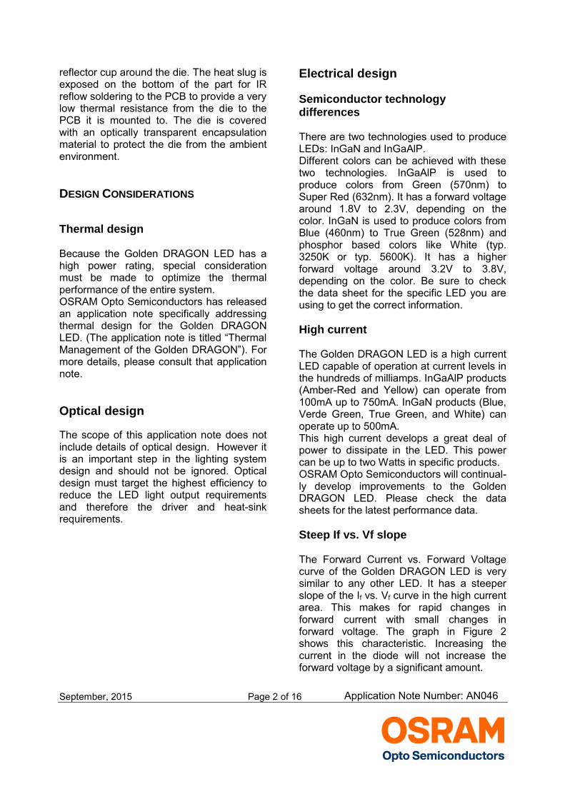
Figure 1 shows the internal structure of the Golden DRAGON LED.
Leads
Die Attach
Bond Wire
Die Molding Compound
Solder Pads
Dielectric Heat Slug
SolderAluminum Plate
Figure 1 Structure of the Golden DRAGON LED
There are large leads for a strong mechani-cal attachment to the printed circuit board (PCB), and to assist proper orientation of the part during reflow soldering.
The semiconductor die is directly attached to the heat slug. This heat slug is cast inside the molding compound, which forms a
Application Note Number: AN046
September, 2015 Page 2 of 16
reflector cup around the die. The heat slug is exposed on the bottom of the part for IR reflow soldering to the PCB to provide a very low thermal resistance from the die to the PCB it is mounted to. The die is covered with an optically transparent encapsulation material to protect the die from the ambient environment.
DESIGN CONSIDERATIONS
Thermal design Because the Golden DRAGON LED has a high power rating, special consideration must be made to optimize the thermal performance of the entire system. OSRAM Opto Semiconductors has released an application note specifically addressing thermal design for the Golden DRAGON LED. (The application note is titled “Thermal Management of the Golden DRAGON”). For more details, please consult that application note.
Optical design
The scope of this application note does not include details of optical design. However it is an important step in the lighting system design and should not be ignored. Optical design must target the highest efficiency to reduce the LED light output requirements and therefore the driver and heat-sink requirements.
Electrical design
Semiconductor technology differences There are two technologies used to produce LEDs: InGaN and InGaAlP. Different colors can be achieved with these two technologies. InGaAlP is used to produce colors from Green (570nm) to Super Red (632nm). It has a forward voltage around 1.8V to 2.3V, depending on the color. InGaN is used to produce colors from Blue (460nm) to True Green (528nm) and phosphor based colors like White (typ. 3250K or typ. 5600K). It has a higher forward voltage around 3.2V to 3.8V, depending on the color. Be sure to check the data sheet for the specific LED you are using to get the correct information.
High current The Golden DRAGON LED is a high current LED capable of operation at current levels in the hundreds of milliamps. InGaAlP products (Amber-Red and Yellow) can operate from 100mA up to 750mA. InGaN products (Blue, Verde Green, True Green, and White) can operate up to 500mA. This high current develops a great deal of power to dissipate in the LED. This power can be up to two Watts in specific products. OSRAM Opto Semiconductors will continual-ly develop improvements to the Golden DRAGON LED. Please check the data sheets for the latest performance data.
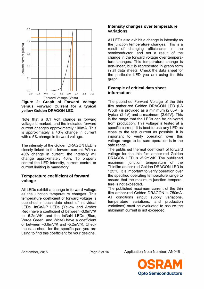
Steep If vs. Vf slope The Forward Current vs. Forward Voltage curve of the Golden DRAGON LED is very similar to any other LED. It has a steeper slope of the If vs. Vf curve in the high current area. This makes for rapid changes in forward current with small changes in forward voltage. The graph in Figure 2 shows this characteristic. Increasing the current in the diode will not increase the forward voltage by a significant amount.
Application Note Number: AN046
September, 2015 Page 3 of 16
F
orw
ard
curr
ent (A
mps)
Forward Voltage (Volts)
0.0 0.4 0.8 1.2 1.6 2.0 2.4 2.8 3.2
0.0
0.1
0.2
0.3
0.4
0.5
Figure 2: Graph of Forward Voltage versus Forward Current for a typical yellow Golden DRAGON LED. Note that a 0.1 Volt change in forward voltage is marked, and the indicated forward current changes approximately 100mA. This is approximately a 40% change in current with a 5% change in forward voltage. The intensity of the Golden DRAGON LED is closely linked to the forward current. With a 40% change in current, the intensity will change approximately 40%. To properly control the LED intensity, current control or current limiting is mandatory.
Temperature coefficient of forward voltage All LEDs exhibit a change in forward voltage as the junction temperature changes. This temperature coefficient of forward voltage is published in each data sheet of individual LEDs. InGaAlP LEDs (Yellow and Amber Red) have a coefficient of between -3.0mV/K to -5.2mV/K, and the InGaN LEDs (Blue, Verde Green, and White) have a coefficient of between –3.6mV/K and -5.2mV/K. Check the data sheet for the specific part you are using to find this coefficient for your designs.
Intensity changes over temperature variations All LEDs also exhibit a change in intensity as the junction temperature changes. This is a result of changing efficiencies in the semiconductor, and not a result of the change in the forward voltage over tempera-ture changes. This temperature change is non-linear, but is represented in graph form in all data sheets. Check the data sheet for the particular LED you are using for this graph.
Example of critical data sheet information The published Forward Voltage of the thin film amber-red Golden DRAGON LED (LA W5SF) is provided as a minimum (2.05V), a typical (2.4V) and a maximum (2.65V). This is the range that the LEDs can be delivered from production. This voltage is tested at a specific current. It is best to use any LED as close to the test current as possible. It is important to verify operation over this voltage range to be sure operation is in the safe range. The published thermal coefficient of forward voltage for the thin film amber-red Golden DRAGON LED is -5.2mV/K. The published maximum junction temperature of the Thinfilm amber-red Golden DRAGON LED is 125°C. It is important to verify operation over the specified operating temperature range to assure that the maximum junction tempera-ture is not exceeded. The published maximum current of the thin film amber-red Golden DRAGON is 750mA. All conditions (input supply variations, temperature variations, and production variations) must be evaluated to assure the maximum current is not exceeded.
Application Note Number: AN046
September, 2015 Page 4 of 16
HOW TO DRIVE A HIGH CURRENT LED
LIKE THE GOLDEN DRAGON LED
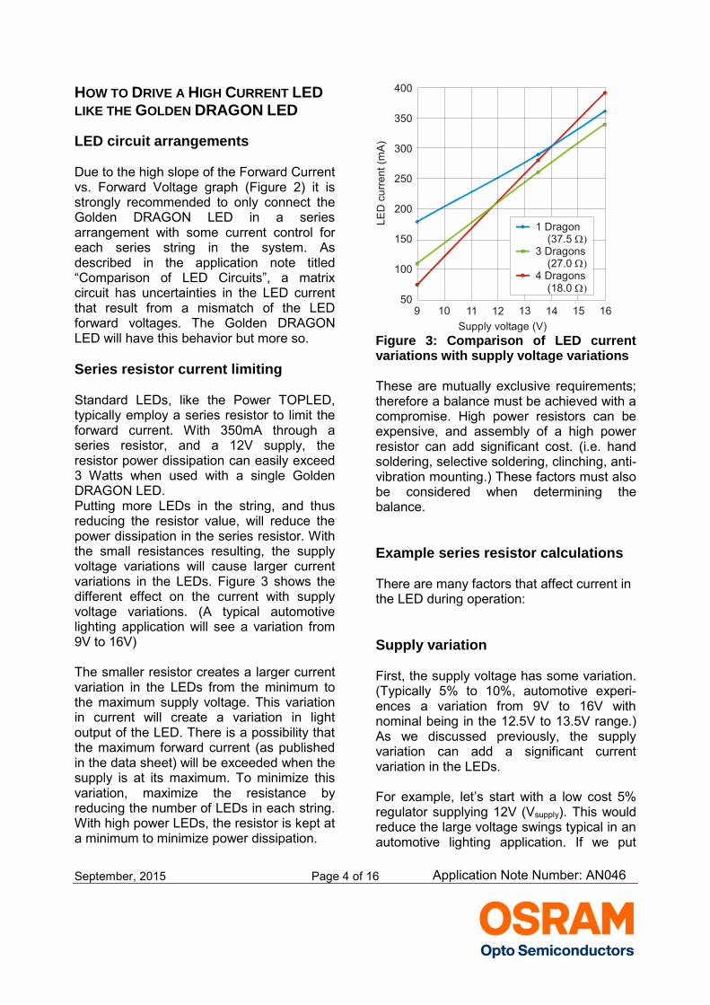
LED circuit arrangements Due to the high slope of the Forward Current vs. Forward Voltage graph (Figure 2) it is strongly recommended to only connect the Golden DRAGON LED in a series arrangement with some current control for each series string in the system. As described in the application note titled “Comparison of LED Circuits”, a matrix circuit has uncertainties in the LED current that result from a mismatch of the LED forward voltages. The Golden DRAGON LED will have this behavior but more so.
Series resistor current limiting Standard LEDs, like the Power TOPLED, typically employ a series resistor to limit the forward current. With 350mA through a series resistor, and a 12V supply, the resistor power dissipation can easily exceed 3 Watts when used with a single Golden DRAGON LED. Putting more LEDs in the string, and thus reducing the resistor value, will reduce the power dissipation in the series resistor. With the small resistances resulting, the supply voltage variations will cause larger current variations in the LEDs. Figure 3 shows the different effect on the current with supply voltage variations. (A typical automotive lighting application will see a variation from 9V to 16V) The smaller resistor creates a larger current variation in the LEDs from the minimum to the maximum supply voltage. This variation in current will create a variation in light output of the LED. There is a possibility that the maximum forward current (as published in the data sheet) will be exceeded when the supply is at its maximum. To minimize this variation, maximize the resistance by reducing the number of LEDs in each string. With high power LEDs, the resistor is kept at a minimum to minimize power dissipation.
400
350
300
250
200
150
100
509 10 11 12 13 14 15 16
Supply voltage (V)
LE
D c
urr
ent
(mA
)
1 Dragon
3 Dragons
4 Dragons
(37.5
(18.0
(27.0
Figure 3: Comparison of LED current variations with supply voltage variations These are mutually exclusive requirements; therefore a balance must be achieved with a compromise. High power resistors can be expensive, and assembly of a high power resistor can add significant cost. (i.e. hand soldering, selective soldering, clinching, anti-vibration mounting.) These factors must also be considered when determining the balance.
Example series resistor calculations There are many factors that affect current in the LED during operation:
Supply variation First, the supply voltage has some variation. (Typically 5% to 10%, automotive experi-ences a variation from 9V to 16V with nominal being in the 12.5V to 13.5V range.) As we discussed previously, the supply variation can add a significant current variation in the LEDs. For example, let’s start with a low cost 5% regulator supplying 12V (Vsupply). This would reduce the large voltage swings typical in an automotive lighting application. If we put
Application Note Number: AN046
September, 2015 Page 5 of 16
three LEDs in a string, each with 2.4V (Vf typical for a thin film amber-red golden DRAGON LED), the series resistor will have a 4.8V (Vresistor) drop at 0.350A (Idiode). This results in a 13.7Ohm resistor dissipating 1.68W (Presistor).
WattsAVP
IVP
A
VR
I
VR
VVVV
VnVV
diode
resistor
68.1350.0*8.4
*
7.13350.0
8.4
8.44.2*312
*
resistor
dioderesistorresistor
resistor
diodesupplyresistor
At the limits of the regulator tolerance, the supply voltage increases only 0.6V (Vsupply = 12.6V maximum). The voltage dropped across the resistor increases to 5.4V, and the current increases by 0.044A. The LED now passes 394mA.
AVI
VI
VVVV
VnVV
394.07.13/4.5
Resistance/
4.54.2*36.12
*
diode
resistordiode
resistor
diodesupplyresistor
Temperature Variation The second factor affecting LED current is the temperature coefficient of the forward voltage of the LED. The data sheet for every LED gives a coefficient for the forward voltage with respect to the junction temperature. At higher temperatures, the forward voltage of the LED will decrease. For the InGaAlP thin film amber-red LED, the coefficient is –5.2mV/K.
VLEDsV
VKKV
KT
9.033.0
3.060/0052.0
60
With a temperature rise of 60K above room temperature, the forward voltage of each LED drops 0.3V. With three LEDs in a string, (in an attempt to reduce power dissipation in the series resistor) the forward voltage across the string will drop 0.9V as a result of the temperature change. The effects of supply variation and tempera-ture variation add with a 5% tolerance on a 12V supply, and a 60K temperature increase, there is a possible total variation of 1.5V across the series resistor. This increases the current in the LEDs by a total of 0.11A. The LED now is passing 0.46A.
Production variation The third factor affecting LED current is production variation of its forward voltage. The data sheet of the Thinfilm amber-red Golden DRAGON LED gives a room temperature forward voltage variation of 0.6V. With a design targeting the nominal value, this can be seen as a ±0.3V tolerance. This voltage change adds with the first two effects creating a possible total variation of 1.84V across the series resistor in this application.
0.3V----Production
0.9V----Temperature
0.6V----Supply
0.3 + 0.9V + 0.6V = 1.8V So, the voltage across the resistor can increase by 1.8V. The current in the LED is now 0.48A. This is not yet at the maximum current published for the thin film amber-red Golden DRAGON LED, but heat dissipation at this current level may cause the maximum junction temperature to be exceeded. This is still significantly above the design intent of the LED. The design must account for this much variation to prevent LED damage. The power dissipated in the LED and resistor will increase substantially, and must be taken into consideration. The current could also decrease when these tolerances move in the
Application Note Number: AN046
September, 2015 Page 6 of 16
opposite direction. If all the tolerances were in the opposite direction, the LED current would drop to 0.2A. This could create problems from intensity variation and the specification may not be satisfied. Special consideration must be given to these factors to be sure the LED’s maximum current rating and the maximum junction temperature are not exceeded at any time in the application when using a series resistor. This means the LED must be used at a nominal level far below its capacity. Using the Golden DRAGON LED at a reduced capacity with a series resistor will require more LEDs. This can significantly increase system costs. In most applications, the cost saved by using only the needed Golden DRAGON LEDs and eliminating the special assembly costs of a high power resistor, will easily cover the cost of a current control supply.
CURRENT CONTROL The current control supply can often be assembled on the same board as the LEDs to save on assembly costs. When doing this, ensure the current control supply does not excessively heat the LEDs. In this example, the voltage regulator used could have been configured as a current source with no added cost to the system. If the regulator had been eliminated from the example, then the wide variations typical for an automotive application (9V to 16V) would have overstressed the LED more than what we saw in the example. Designing in a current control supply has several benefits:
Reduced LED count and thus lower costs
The current control supply can be all SMT components, and a high power resistor can be eliminated. This significantly reduces assembly
complexity. Again this will give a cost savings.
Reduced power dissipation at the higher temperature, higher supply voltage and lower LED forward voltage conditions (as compared to a resistor drive).
Constant intensity output will give a better, more uniform appearance, and can better satisfy a tight tolerance specification.
Current control methods There are two technologies to consider when designing a current control driver for the Golden DRAGON LED. The first is a linear current control driver, and the second is a switch mode current control driver. This application note will consider the basics of using both, but will not detail designs. Please seek information from the individual IC manufacturers for designing with their parts.
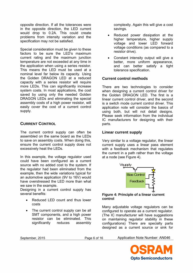
Linear current supply Very similar to a voltage regulator, the linear current supply uses a linear pass element with a feedback mechanism that regulates the current in a path rather than the voltage at a node (see Figure 4).
Bias Control
Feedback
Vsupply
Figure 4: Principle of a linear current control Many adjustable voltage regulators can be configured to operate as a current regulator. (The IC manufacturer will have suggestions on maintaining regulator stability in these configurations) There are specialty parts designed as a current source or sink for
Application Note Number: AN046
September, 2015 Page 7 of 16
other applications that can be enlisted to drive an LED (battery chargers, solenoid drivers, etc.). The linear current supply can only be used when the input voltage is always higher than the output voltage. Headroom must also be added to account for drop voltages in the driver circuits. Otherwise there is not enough voltage available to operate the LEDs. The advantages of a linear current supply are its simplicity of design, and low component cost. A linear current supply has a disadvantage in that in regulating current, a large amount of power must be dissipated by the supply. This can occur when there is a large voltage drop across the supply. (This dissipation will always be lower than a resistor drive where the current will increase as the voltage increases.) This often requires a heat sink. Since the Golden DRAGON LED requires a heat sink in most applications, the two can be combined into a single heat sink.
Linear current control supply design example Let’s consider an application example requiring three Golden DRAGON LEDs in a string. (Three LEDs are needed based on minimum light requirements) We will use an input supply voltage of 15V (VSupply). With 3 LEDs (n) each having a 2.2V forward voltage (Vf), the current control supply (or driver) is left to drop the remaining voltage (Vdriver).
WattsAVP
IVP
VVVV
VnVV
94.2350.0*4.8
*
4.82.2*315
*
driver
diodedriverdriver
driver
diodesupplydriver
The driver needs to drop 8.4V, so the power dissipated is 2.94W, which can be very difficult to dissipate depending on the maximum ambient temperature.
To reduce this dissipation, add an LED to the string so the power is used by the additional LED to generate light, not being wasted in the supply. The power will still need to be dissipated by the additional LED, but more light is generated for use. This additional light reduces the required current. This means the Golden DRAGON LEDs only need to run at about 280mA, and there is still a surplus of light. By adding one LED to the string, the supply now has to drop 6.2V. In addition, with the LEDs operating at 280mA, the power to dissipate in the current control supply is 1.74W. This is manageable with only PCB copper area around the driver IC, or a small heat sink depending on the maximum ambient temperature of the system. From this example we can see that adding a single LED to the string can make the whole system more thermally manageable. This improves the overall system thermal man-agement by reducing power loss in the driver and increasing margin of the design. This will improve the reliability of the entire lighting system. In every case, the designer must evaluate all three parts of the design: thermal system performance, electrical system performance, and system assembly efficiency, to properly optimize the system.
Examples of Linear current control supply circuits:
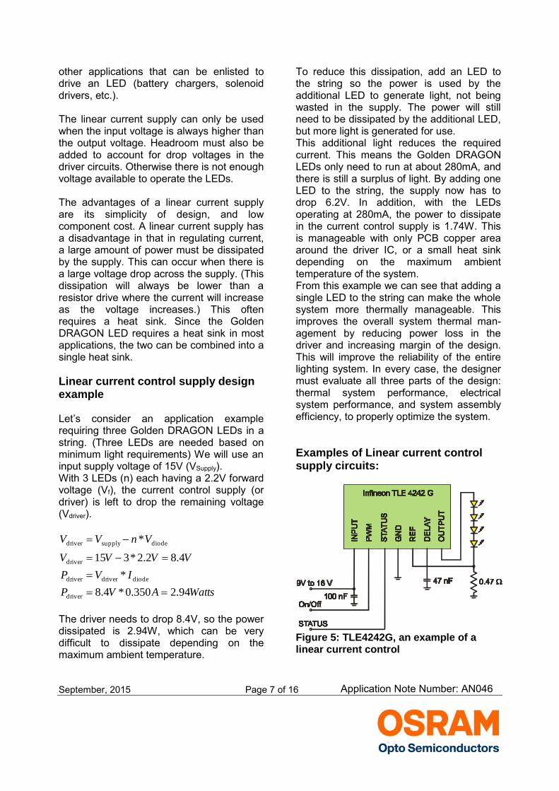
Figure 5: TLE4242G, an example of a linear current control
Application Note Number: AN046
September, 2015 Page 8 of 16
Figure 5 is an example of a linear current control, the TLE 4242G from Infineon Technologies. This circuit offers simplicity, and is suitable for use in automotive applications. There is a PWM input to control LED brightness, or with a constant low, the part will shut down and consume less than 1μA. There is also a status feedback for diagnostics. The part includes over-temperature and short circuit protection.
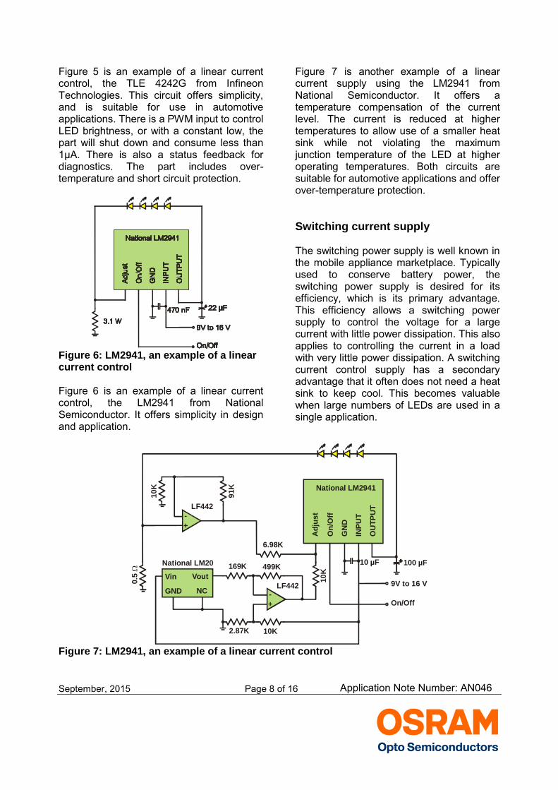
Figure 6: LM2941, an example of a linear current control Figure 6 is an example of a linear current control, the LM2941 from National Semiconductor. It offers simplicity in design and application.
Figure 7 is another example of a linear current supply using the LM2941 from National Semiconductor. It offers a temperature compensation of the current level. The current is reduced at higher temperatures to allow use of a smaller heat sink while not violating the maximum junction temperature of the LED at higher operating temperatures. Both circuits are suitable for automotive applications and offer over-temperature protection.
Switching current supply The switching power supply is well known in the mobile appliance marketplace. Typically used to conserve battery power, the switching power supply is desired for its efficiency, which is its primary advantage. This efficiency allows a switching power supply to control the voltage for a large current with little power dissipation. This also applies to controlling the current in a load with very little power dissipation. A switching current control supply has a secondary advantage that it often does not need a heat sink to keep cool. This becomes valuable when large numbers of LEDs are used in a single application.
National LM20
Vin
GND
Vout
NC
10 Fµ 100 Fµ
9V to 16 V
On/Off
0.5
+
-
National L 2941M
Ad
jus
t
On
/Off
GN
D
INP
UT
OU
TP
UT
LF442
LF442
+
-
10
K
91
K
6.98K
499K169K
2.87K 10K
10
K
Figure 7: LM2941, an example of a linear current control
Application Note Number: AN046
September, 2015 Page 9 of 16
A switching current control supply is a frequency-based device. This adds to the complexity of the design. It must be carefully designed to be frequency stable, and not radiate electromagnetic noise in undesirable spectrums. The latter is known as designing for electromagnetic compatibility (EMC). Individual manufacturers of switching power supply integrated circuits can provide assistance in both of these requirements. Compared to a linear current control supply, the switching current control supply can have a higher cost and more components. This cost disadvantage can often be offset by not needing a heat sink and redundant linear current control drivers, but this must always be evaluated for each application.
Different topologies of switching power supply current control There are three primary topologies of switching power supplies:
The buck regulator The boost regulator The buck-boost regulator
Determining which topology to use in the design is based on the input and output voltage levels: The buck regulator can only function when the supply voltage is always higher than the load supply plus some voltage drop from the buck circuitry. The boost regulator can only function when the supply voltage is always lower than the output voltage minus some voltage drops from the boost circuitry. The buck-boost regulator can function when the supply voltage can vary above or below the load voltage, or when the load voltage can vary above and below the supply voltage. The former can occur when multiple sources are used, or a source varies widely. The later can occur with a current control supply.
The buck topology is used most often when the power dissipated in a linear current control supply would be excessive. The boost topology should be used when there are too many LEDs to drive using a linear current control supply. As the number of LEDs increases, and the cost (and heat) of the linear current control supplies also increases, a cross-over point is quickly found where the switching current control supply is significantly cheaper than the linear current control supplies. The LEDs are arranged all in one string, which makes the output voltage higher than the input supply voltage. Putting more LEDs in a string reduces the number of strings in the system, and therefore reduces the total number of current control drivers needed. The buck-boost topology is often used in applications where the application is powered from the AC mains and the rectified voltage varies from 0V to the peak voltage. This topology is also used when the application must operate from many varying supplies (i.e. 120VAC and 240VAC systems, or 12V, 24V and 48V DC systems). Most switching power supply integrated circuits can be used in multiple topologies. The manufacturer can provide optional configuration information of their parts. Again, in every case, the designer must evaluate all three portions of the design: thermal system performance, electrical system performance, and system assembly efficiency to properly optimize the system.
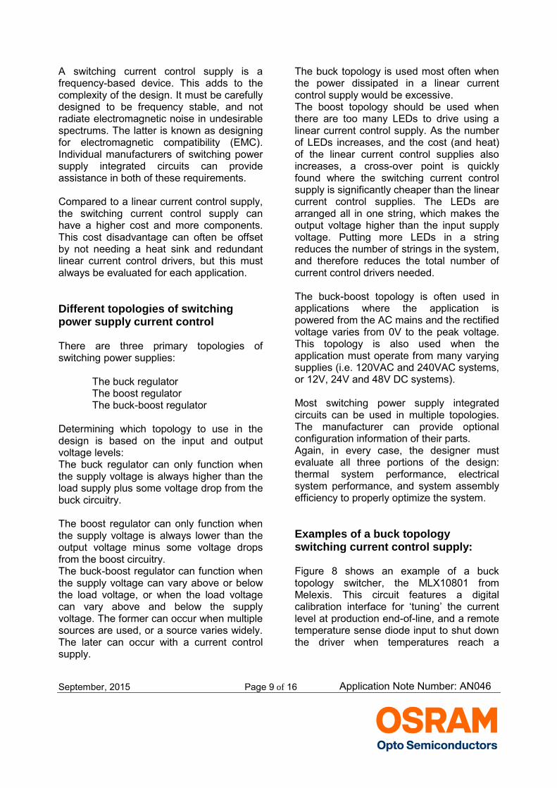
Examples of a buck topology switching current control supply: Figure 8 shows an example of a buck topology switcher, the MLX10801 from Melexis. This circuit features a digital calibration interface for ‘tuning’ the current level at production end-of-line, and a remote temperature sense diode input to shut down the driver when temperatures reach a
Application Note Number: AN046
September, 2015 Page 10 of 16
specified maximum. This part is suitable for automotive applications.
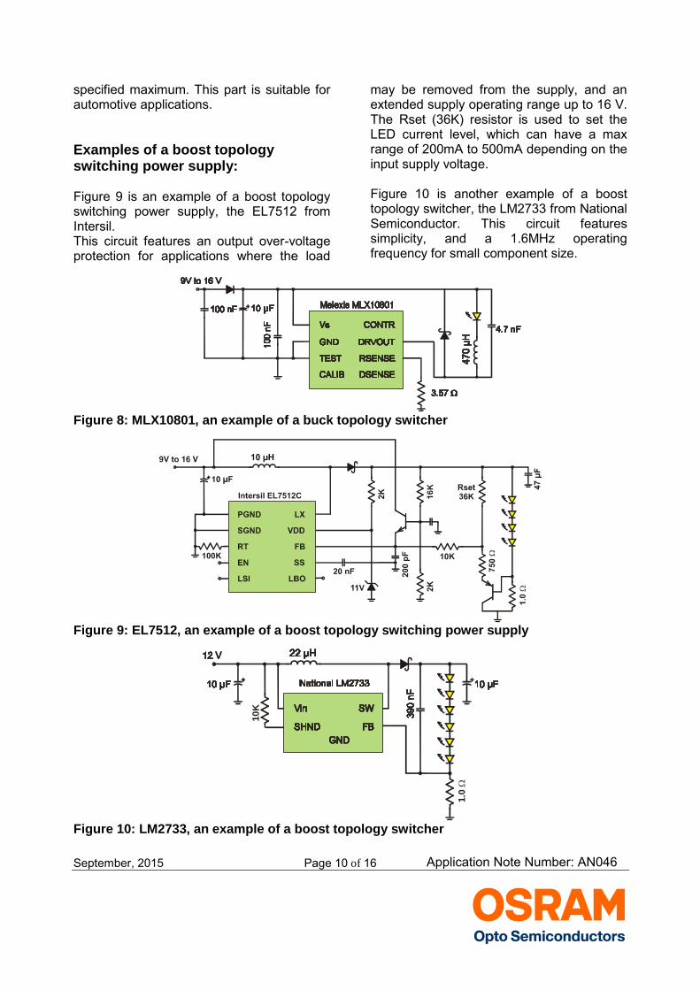
Examples of a boost topology switching power supply: Figure 9 is an example of a boost topology switching power supply, the EL7512 from Intersil. This circuit features an output over-voltage protection for applications where the load
may be removed from the supply, and an extended supply operating range up to 16 V. The Rset (36K) resistor is used to set the LED current level, which can have a max range of 200mA to 500mA depending on the input supply voltage. Figure 10 is another example of a boost topology switcher, the LM2733 from National Semiconductor. This circuit features simplicity, and a 1.6MHz operating frequency for small component size.
Figure 8: MLX10801, an example of a buck topology switcher
Figure 9: EL7512, an example of a boost topology switching power supply
1.0
10
K
Figure 10: LM2733, an example of a boost topology switcher
Application Note Number: AN046
September, 2015 Page 11 of 16
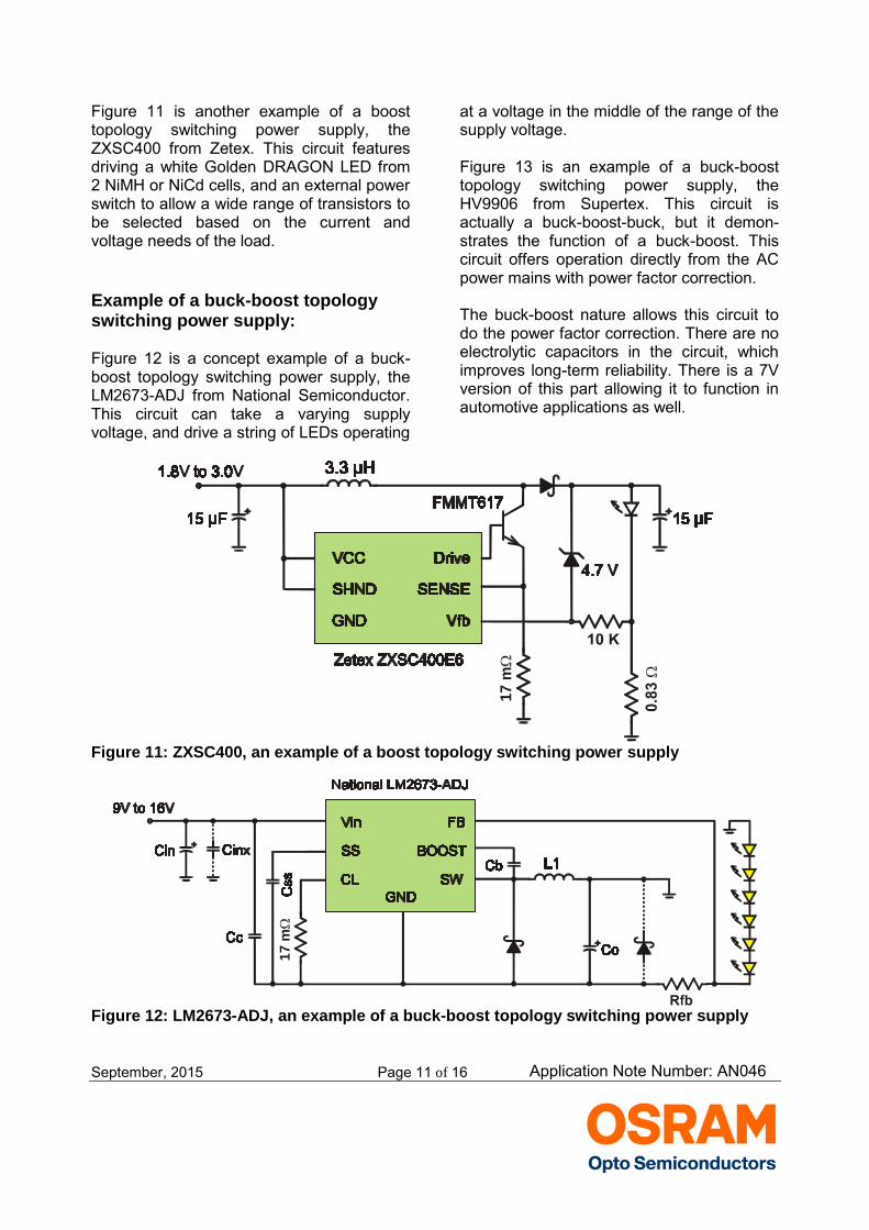
Figure 11 is another example of a boost topology switching power supply, the ZXSC400 from Zetex. This circuit features driving a white Golden DRAGON LED from 2 NiMH or NiCd cells, and an external power switch to allow a wide range of transistors to be selected based on the current and voltage needs of the load.
Example of a buck-boost topology switching power supply: Figure 12 is a concept example of a buck-boost topology switching power supply, the LM2673-ADJ from National Semiconductor. This circuit can take a varying supply voltage, and drive a string of LEDs operating
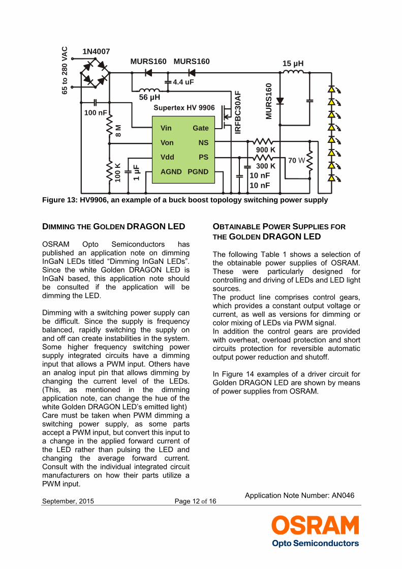
at a voltage in the middle of the range of the supply voltage. Figure 13 is an example of a buck-boost topology switching power supply, the HV9906 from Supertex. This circuit is actually a buck-boost-buck, but it demon-strates the function of a buck-boost. This circuit offers operation directly from the AC power mains with power factor correction. The buck-boost nature allows this circuit to do the power factor correction. There are no electrolytic capacitors in the circuit, which improves long-term reliability. There is a 7V version of this part allowing it to function in automotive applications as well.
17
m
Figure 11: ZXSC400, an example of a boost topology switching power supply
17
m
Figure 12: LM2673-ADJ, an example of a buck-boost topology switching power supply
Application Note Number: AN046
September, 2015 Page 12 of 16
100 nF
65
to
280
VA
C
56 µH
8 M Vin
Von
Vdd
AGND
Gate
NS
PS
PGND
70 W
10
0 K
1N4007
MURS160 15 µH
MU
RS
16
04.4 uF
IRF
BC
30
AF
1 µ
F
MURS160
10 nF
10 nF
Figure 13: HV9906, an example of a buck boost topology switching power supply
DIMMING THE GOLDEN DRAGON LED OSRAM Opto Semiconductors has published an application note on dimming InGaN LEDs titled “Dimming InGaN LEDs”. Since the white Golden DRAGON LED is InGaN based, this application note should be consulted if the application will be dimming the LED. Dimming with a switching power supply can be difficult. Since the supply is frequency balanced, rapidly switching the supply on and off can create instabilities in the system. Some higher frequency switching power supply integrated circuits have a dimming input that allows a PWM input. Others have an analog input pin that allows dimming by changing the current level of the LEDs. (This, as mentioned in the dimming application note, can change the hue of the white Golden DRAGON LED’s emitted light) Care must be taken when PWM dimming a switching power supply, as some parts accept a PWM input, but convert this input to a change in the applied forward current of the LED rather than pulsing the LED and changing the average forward current. Consult with the individual integrated circuit manufacturers on how their parts utilize a PWM input.
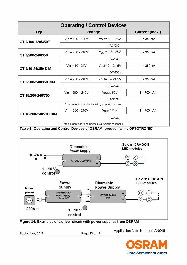
OBTAINABLE POWER SUPPLIES FOR
THE GOLDEN DRAGON LED The following Table 1 shows a selection of the obtainable power supplies of OSRAM. These were particularly designed for controlling and driving of LEDs and LED light sources. The product line comprises control gears, which provides a constant output voltage or current, as well as versions for dimming or color mixing of LEDs via PWM signal. In addition the control gears are provided with overheat, overload protection and short circuits protection for reversible automatic output power reduction and shutoff. In Figure 14 examples of a driver circuit for Golden DRAGON LED are shown by means of power supplies from OSRAM.
Application Note Number: AN046
September, 2015 Page 13 of 16
Operating / Control Devices
Typ Voltage Current (max.)
OT 9/100-120/350E Vin = 100 - 120V Vout= 1.8 - 25V I = 350mA
(AC/DC)
OT 9/200-240/350 Vin = 200 - 240V Vout= 1.8 - 25V I = 350mA
(AC/DC)
OT 9/10-24/350 DIM Vin = 10 - 24V Vout= 0 – 24.5V I = 350mA
(DC/DC)
OT 9/200-240/350 DIM Vin = 200 - 240V Vout= 0 – 24.5V I = 350mA
(AC/DC)
OT 35/200-240/700 Vin = 200 – 240V Vout ≤ 50V I = 700mA*
(AC/DC)
* the current has to be limited by a resistor or balun
OT 18/200-240/700 DIM Vin = 200 - 240V Vout ≤ 25V I = 700mA*
(AC/DC)
* the current has to be limited by a resistor or or balun
Table 1: Operating and Control Devices of OSRAM (product family OPTOTRONIC)
Figure 14: Examples of a driver circuit with power supplies from OSRAM
Application Note Number: AN046
September, 2015 Page 14 of 16
SUMMARY
To minimize lighting system costs, and maximize performance, all areas must be evaluated and optimized: thermal design, electrical design, optical design and system assembly efficiency.
The Golden DRAGON LED can be driven with a series resistor, but at a greatly reduced capacity. It needs a current control supply to maintain reliable and consistent performance in most applications.
The lighting system thermal performance is key: keep the thermal resistance of the system as low as economically possible for best thermal efficiency to keep the LED and current control parts count low. Good thermal management will also improve the reliability of the system.
Design the system to keep the LED’s junction temperature as low as possible, because a cool LED generates more light than a hot LED. In all cases design the system to prevent the LED’s junction tempera-ture from exceeding the rated maximums given in the data sheet.
A linear current control supply is best suited when the load voltage will be just below the input supply voltage (to minimize power dissipation in the current control supply) and when there are only a few strings.
A buck topology current control supply is used in applications where the input supply voltage will always be above the load voltage, and the power dissipated is more than what can be reasonably handled with a linear current control supply.
A boost topology current control supply is used when the input supply voltage will always be below the load voltage, or when there are many LEDs to drive. In the later case, with many strings, several supplies would be needed, or a current divider would be needed. Putting the LEDs into one longer string reduces the total supply need, but the voltage increases above the input supply. This then requires a boost topology current control supply.
A buck-boost topology current control supply is used when the supply and load voltages will not consistently be higher or lower than one another. In some cases, adding LEDs to the strings and using a boost topology current control supply can offer a better solution.
Application Note Number: AN046
September, 2015 Page 15 of 16
APPENDIX
Don't forget: LED Light for you is your place to be whenever you are looking for information or worldwide partners for your LED Lighting project.
www.ledlightforyou.com
Revision History
Date Revision History
Feb. 2007 Release of application note
Sept. 2015 Change of Company Info & Disclaimer
Authors: Timothy Dunn, Andreas Stich ABOUT OSRAM OPTO SEMICONDUCTORS OSRAM, Munich, Germany is one of the two leading light manufacturers in the world. Its subsidiary, OSRAM Opto Semiconductors GmbH in Regensburg (Germany), offers its customers solutions based on semiconductor technology for lighting, sensor and visualization applications. OSRAM Opto Semiconductors has production sites in Regensburg (Germany), Penang (Malaysia) and Wuxi (China). Its headquarters for North America is in Sunnyvale (USA), and for Asia in Hong Kong. OSRAM Opto Semiconductors also has sales offices throughout the world. For more information go to www.osram-os.com.
Application Note Number: AN046
September, 2015 Page 16 of 16
DISCLAIMER PLEASE CAREFULLY READ THE BELOW TERMS AND CONDITIONS BEFORE USING THE INFORMATION SHOWN HEREIN. IF YOU DO NOT AGREE WITH ANY OF THESE TERMS AND CONDITIONS, DO NOT USE THE INFORMATION. The information provided in this general information document was formulated using the utmost care; however, it is provided by OSRAM Opto Semiconductors GmbH on an “as is” basis. Thus, OSRAM Opto Semiconductors GmbH does not expressly or implicitly assume any warranty or liability whatsoever in relation to this information, including – but not limited to – warranties for correctness, completeness, marketability, fitness for any specific purpose, title, or non-infringement of rights. In no event shall OSRAM Opto Semiconductors GmbH be liable – regardless of the legal theory – for any direct, indirect, special, incidental, exemplary, consequential, or punitive damages arising from the use of this information. This limitation shall apply even if OSRAM Opto Semiconductors GmbH has been advised of possible damages. As some jurisdictions do not allow the exclusion of certain warranties or limitations of liabilities, the above limitations and exclusions might not apply. In such cases, the liability of OSRAM Opto Semiconductors GmbH is limited to the greatest extent permitted in law. OSRAM Opto Semiconductors GmbH may change the provided information at any time without giving notice to users and is not obliged to provide any maintenance or support related to the provided information. The provided information is based on special conditions, which means that the possibility of changes cannot be precluded. Any rights not expressly granted herein are reserved. Other than the right to use the information provided in this document, no other rights are granted nor shall any obligations requiring the granting of further rights be inferred. Any and all rights and licenses regarding patents and patent applications are expressly excluded. It is prohibited to reproduce, transfer, distribute, or store all or part of the content of this document in any form without the prior written permission of OSRAM Opto Semiconductors GmbH unless required to do so in accordance with applicable law.
Application Note Number: AN046