
Widely-tunable, narrow-linewidth III-V/silicon hybrid external-cavity laser for coherent communication HANG GUAN,1,2,3* ARI NOVACK,1,2,3 TAL GALFSKY,2 YANGJIN MA,2 SAEED FATHOLOLOUMI,2 ALEXANDRE HORTH,2 TAM N. HUYNH,2 JOSE ROMAN,2 RUIZHI SHI,2 MICHAEL CAVERLEY,2 YANG LIU,2 THOMAS BAEHR-JONES,2 KEREN BERGMAN,1 AND MICHAEL HOCHBERG2
1Department of Electrical Engineering, Columbia University, New York, NY 10027, USA 2Elenion Technologies, New York, NY 10016, USA 3These authors contributed equally *[email protected]
Abstract: We demonstrate a III-V/silicon hybrid external cavity laser with a tuning range larger than 60 nm at the C-band on a silicon-on-insulator platform. A III-V semiconductor gain chip is hybridized into the silicon chip by edge-coupling the silicon chip through a Si3N4 spot size converter. The demonstrated packaging method requires only passive alignment and is thus suitable for high-volume production. The laser has a largest output power of 11 mW with a maximum wall-plug efficiency of 4.2%, tunability of 60 nm (more than covering the C-band), and a side-mode suppression ratio of 55 dB (>46 dB across the C-band). The lowest measured linewidth is 37 kHz (<80 kHz across the C-band), which is the narrowest linewidth using a silicon-based external cavity. In addition, we successfully demonstrate all silicon-photonics-based transmission of 34 Gbaud (272 Gb/s) dual-polarization 16-QAM using our integrated laser and silicon photonic coherent transceiver. The results show no additional penalty compared to commercially available narrow linewidth tunable lasers. To the best of our knowledge, this is the first experimental demonstration of a complete silicon photonic based coherent link. This is also the first experimental demonstration of >250 Gb/s coherent optical transmission using a silicon micro-ring-based tunable laser. © 2018 Optical Society of America
OCIS codes: (250.5960) Semiconductor lasers; (250.5300) Photonic integrated circuits; (140.3600) Lasers, tunable; (060.1660) Coherent communications.
References and links 1. M. Hochberg and T. Baehr-Jones, “Towards fabless silicon photonics,” Nat. Photonics 4(8), 492–494 (2010). 2. M. Asghari and A. V. Krishnamoorthy, “Silicon photonics: energy-efficient communication,” Nat. Photonics
5(5), 268–270 (2011). 3. C. R. Doerr, “Silicon photonic integration in telecommunications,” Front. Phys. 3, 37 (2015). 4. D. Thomson, A. Zilkie, J. E. Bowers, T. Komljenovic, G. T. Reed, L. Vivien, D. Marris-Morini, E. Cassan, L.
Virot, J.-M. Fédéli, J.-M. Hartmann, J. H. Schmid, D.-X. Xu, F. Boeuf, P. O’Brien, G. Z. Mashanovich, and M. Nedeljkovic, “Roadmap on silicon photonics,” J. Opt. 18(7), 073003 (2016).
5. D. Nikolova, S. Rumley, D. Calhoun, Q. Li, R. Hendry, P. Samadi, and K. Bergman, “Scaling silicon photonic switch fabrics for data center interconnection networks,” Opt. Express 23(2), 1159–1175 (2015).
6. K. Wen, P Samadi, S. Rumley, C. P. Chen, Y. Shen, M. Bahadori, K. Bergman, and J. Wilke, "Flexfly: Enabling a reconfigurable dragonfly through silicon photonics,"" In International Conference for High Performance Computing, Networking, Storage and Analysis (2016), pp. 166-177.
7. S. Rumley, D. Nikolova, R. Hendry, Q. Li, D. Calhoun, and K. Bergman, “Silicon photonics for exascale systems,” J. Lightwave Technol. 33(3), 547-562 (2015).
8. H.-F. Liu, “Integrated silicon photonics links for high bandwidth data transportation,” in Optical Fiber Communication Conference (2014), paper Th1D.1.
9. M. Mazzini, M. Traverso, M. Webster, C. Muzio, S. Anderson, P. Sun, D. Siadat, D. Conti, A. Cervasio, S. Pfnuer, J. Stayt, M. Nyland, C. Togami, K. Yanushefski, and T. Daugherty, “25GBaud PAM-4 error free transmission over both single mode fiber and multimode fiber in a QSFP form factor based on silicon photonics,” in Optical Fiber Communication Conference (2015), paper Th5B.3.
10. A. Ramaswamy, J. E. Roth, E. J. Norberg, R. S. Guzzon, J. H. Shin, J. T. Imamura, B. R. Koch, D. K. Sparacin, G. A. Fish, B. G. Lee, R. Rimolo-Donadio, C. W. Baks, A. Rylyakov, J. Proesel, M. Meghelli, and C. L. Schow, “A WDM 4x28Gbps integrated silicon photonic transmitter driven by 32nm CMOS driver ICs,” in Optical Fiber Communication Conference (2015), paper Th5B.5.
11. B. Milivojevic, C. Raabe, A. Shastri, M. Webster, P. Metz, S. Sunder, B. Chattin, S. Wiese, B. Dama, and K. Shastri, “112Gb/s DP-QPSK transmission over 2427km SSMF using small size silicon photonics IQ modulator and low power CMOS driver,” in Optical Fiber Communication Conference (2013), paper OTh1D.1.
12. C. R. Doerr, L. Chen, D. Vermeulen, T. Nielsen, S. Azemati, S. Stulz, G. McBrien, X. Xu, B. Mikkelsen, M. Givehchi, C. Rasmussen, and S. Y. Park, “Single-chip silicon photonics 100-Gb/s coherent transceiver,” in Optical Fiber Communication Conference (2014), paper Th5C.1.
13. P. Dong, X. Liu, S. Chandrasekhar, L. L. Buhl, R. Aroca, and Y.-K. Chen, “Monolithic silicon photonic integrated circuits for compact 100+ Gb/s coherent optical receivers and transmitters,” IEEE J. Sel. Top. Quantum Electron. 20(4), 1–8 (2014).
14. C. Doerr, J. Heanue, L. Chen, R. Aroca, S. Azemati, G. Ali, G. McBrien, L. Chen, B. Guan, H. Zhang, and X. Zhang, “Silicon photonics coherent transceiver in a ball-grid array package,” in Optical Fiber Communication Conference (2017), paper Th5D.5.
15. C. R. S. Fludger, E. S. Vercelli, G. Marenco, A. Della Torre, T. Duthel, and T. Kupfer, “1Tb/s Real-Time 4× 40 Gbaud DP-16QAM Super-Channel Using CFP2-ACO Pluggable Modules Over 625 km of Standard Fiber,” J. Lightwave Technol., 35(4), 949-954 (2017).
16. R. E. Camacho-Aguilera, Y. Cai, N. Patel, J. T. Bessette, M. Romagnoli, L. C. Kimerling, and J. Michel, “An electrically pumped germanium laser,” Opt. Express 20(10), 11316–11320 (2012).
17. S. Wirths, R. Geiger, N. von den Driesch, G. Mussler, T. Stoica, S. Mantl, Z. Ikonic, M. Luysberg, S. Chiussi, J. M. Hartmann, H. Sigg, J. Faist, D. Buca, and D. Grützmacher, “Lasing in direct-bandgap GeSn alloy grown on Si,” Nat. Photonics 9(2), 88–92 (2015).
18. S. Chen, W. Li, J. Wu, Q. Jiang, M. Tang, S. Shutts, S. N. Elliott, A. Sobiesierski, A. J. Seeds, I. Ross, P. M. Smowton, and H. Liu, “Electrically pumped continuous-wave III–V quantum dot lasers on silicon,” Nat. Photonics 10(5), 307–311 (2016).
19. A. Y. Liu, C. Zhang, J. Norman, A. Snyder, D. Lubyshev, J. M. Fastenau, A. W. Liu, A. C. Gossard, and J. E. Bowers, “High performance continuous wave 1.3 µm quantum dot lasers on silicon,” Appl. Phys. Lett. 104(4), 041104 (2014).
20. E. S. Magden, N. Li, J. D. Bradley, N. Singh, A. Ruocco, G. S. Petrich, G. Leake, D. D. Coolbaugh, E. P. Ippen, M. R. Watts, and L. A. Kolodziejski, “Monolithically-integrated distributed feedback laser compatible with CMOS processing,” Opt. Express, 25(15), 18058-18065 (2017).
21. A. W. Fang, H. Park, O. Cohen, R. Jones, M. J. Paniccia, and J. E. Bowers, “Electrically pumped hybrid AlGaInAs-silicon evanescent laser,” Opt. Express 14(20), 9203–9210 (2006).
22. S. Keyvaninia, G. Roelkens, D. Van Thourhout, C. Jany, M. Lamponi, A. Le Liepvre, F. Lelarge, D. Make, G.- H. Duan, D. Bordel, and J.-M. Fedeli, “Demonstration of a heterogeneously integrated III-V/SOI single wave- length tunable laser,” Opt. Express 21(3), 3784–3792 (2013).
23. J. C. Hulme, J. K. Doylend, and J. E. Bowers, “Widely tunable Vernier ring laser on hybrid silicon,” Opt. Express 21(17), 19718–19722 (2013).
24. T. Creazzo, E. Marchena, S. B. Krasulick, P. Yu, D. Van Orden, J. Y. Spann, C. C. Blivin, L. He, H. Cai, J. M. Dallesasse, R. J. Stone, and A. Mizrahi, “Integrated tunable CMOS laser,” Opt. Express 21(23), 28048–28053 (2013).
25. G. H. Duan, C. Jany, A. Le Liepvre, A. Accard, M. Lamponi, D. Make, P. Kaspar, G. Levaufre, G. Nils, F. Lelarge, J. M. Fedeli, A. Descos, B. Ben Bakir, S. Messaoudene, D. Bordel, S. Menezo, G. de Valicourt, S. Keyvaninia, G. Roelkens, D. Van Thourhout, D. J. Thomson, Y. G. Gardes, and G. T. Reed, “Hybrid III-V on Silicon Lasers for Photonic Integrated Circuits on Silicon,” IEEE J. Sel. Top. Quantum Electron. 20(4), 6100213 (2014).
26. T. Chu, N. Fujioka, and M. Ishizaka, “Compact, lower-power-consumption wavelength tunable laser fabricated with silicon photonic-wire waveguide micro-ring resonators,” Opt. Express 17(16), 14063–14068 (2009).
27. A. J. Zilkie, P. Seddighian, B. J. Bijlani, W. Qian, D. C. Lee, S. Fathololoumi, J. Fong, R. Shafiiha, D. Feng, B. J. Luff, X. Zheng, J. E. Cunningham, A. V. Krishnamoorthy, and M. Asghari, “Power-efficient III-V/silicon external cavity DBR lasers,” Opt. Express 20(21), 23456–23462 (2012).
28. S. Tanaka, S.-H. Jeong, S. Sekiguchi, T. Kurahashi, Y. Tanaka, and K. Morito, “High-output-power, single- wavelength silicon hybrid laser using precise flip-chip bonding technology,” Opt. Express 20(27), 28057–28069 (2012).
29. R. M. Oldenbeuving, E. J. Klein, H. L. Offerhaus, C. J. Lee, H. Song, and K.-J. Boller, “25 kHz narrow spectral bandwidth of a wavelength tunable diode laser with a short waveguide-based external cavity,” Laser Phys. Lett. 10(1), 015804 (2013).
30. B. Snyder, B. Corbett, and P. O’Brien, “Hybrid integration of the wavelength-tunable laser with a silicon photonic integrated circuit,” J. Lightwave Technol. 31(24), 3934–3942 (2013).
31. S. Yang, Y. Zhang, D. W. Grund, G. A. Ejzak, Y. Liu, A. Novack, D. Prather, A. E.-J. Lim, G.-Q. Lo, T. Baehr- Jones, and M. Hochberg, “A single adiabatic microring-based laser in 220 nm silicon-on-insulator,” Opt. Express 22(1), 1172–1180 (2014).
32. Y. Zhang, S. Yang, H. Guan, A. E.-J. Lim, G.-Q. Lo, P. Magill, T. Baehr-Jones, and M. Hochberg, “Sagnac loop mirror and micro-ring based laser cavity for silicon-on-insulator,” Opt. Express 22(15), 17872–17879 (2014).
33. J.-H. Lee, I. Shubin, J. Yao, J. Bickford, Y. Luo, S. Lin, S. S. Djordjevic, H. D. Thacker, J. E. Cunningham, K. Raj, X. Zheng, and A. V. Krishnamoorthy, “High power and widely tunable Si hybrid external-cavity laser for power efficient Si photonics WDM links,” Opt. Express 22(7), 7678–7685 (2014).
34. B. Song, C. Stagarescu, S. Ristic, A. Behfar, and J. Klamkin, “3D integrated hybrid silicon laser,” Opt. Express 24(10), 10435–10444 (2016).
35. S. Lin, X. Zheng, J. Yao, S. S. Djordjevic, J. E. Cunningham, J. H. Lee, I. Shubin, Y. Luo, J. Bovington, D. Y. Lee, and H. D. Thacker, “Efficient, tunable flip-chip-integrated III-V/Si hybrid external-cavity laser array,” Opt. Express, 24(19), 21454-21462 (2016).
36. B. Liu, A. Shakouri, and J. E. Bowers, “Wide tunable double ring resonator coupler lasers,” IEEE Photonics Technol. Lett. 14(5), 600–602 (2002).
37. S. Matsuo and T. Segawa, “Microring-resonator-based widely tunable lasers,” IEEE J. Sel. Top. Quantum Electron. 15(3), 545–554 (2009).
38. Y. Liu, R. Ding, Y. Ma, Y. Yang, Z. Xuan, Q. Li, A. E. Lim, G. Q. Lo, K. Bergman, T. Baehr-Jones, and M. Hochberg, “Silicon Mod-MUX-Ring transmitter with 4 channels at 40 Gb/s,” Opt. Express 22(13), 16431–16438 (2014).
39. A. Yariv, “Universal relations for coupling of optical power between microresonators and dielectric waveguides,” Elect. Lett. 36(4), 321–322 (2000).
40. W. Bogaerts, P. De Heyn, T. Van Vaerenbergh, K. DeVos, S. K. Selvaraja, T. Claes, P. Dumon, P. Bienstman, D. Van Thourhout, and R. Baets, "Silicon microring resonators," Laser Photon. Rev. 6(1), 47-73 (2012).
41. X. Zheng, S. Lin, Y. Luo, J. Yao, G. Li, S. S. Djordjevic, J. Lee, H. D. Thacker, I. Shubin, K. Raj, J. E. Cunningham, and A. V. Krishnamoorthy, “Efficient WDM Laser Sources towards Terabyte/s Silicon Photonic Interconnects,” J. Lightwave Technol. 31(24), 4142–4154 (2013).
42. J. H. Lee, J. Bovington, I. Shubin, Y. Luo, J. Yao, S. Lin, J. E. Cunningham, K. Raj, A. V. Krishnamoorthy, and X. Zheng, “Demonstration of 12.2% wall plug efficiency in uncooled single mode external-cavity tunable Si/III- V hybrid laser,” Opt. Express 23(9), 12079–12088 (2015).
43. J. H. Lee, D. Y. Lee, I. Shubin, J. Bovington, S. S. Djordjevic, S. Lin, Y. Luo, J. Yao, J. E. Cunningham, K. Raj, and A. V. Krishnamoorthy, “III-V/Si hybrid laser stabilization using micro-ring feedback control,” IEEE Photonics J. 8(5), 1-7 (2016).
44. Optical Internetworking Forum, Integrable Tunable Laser Assembly Multi-Source Agreement (OIF-ITLA-MSA- 01.3), (2015).
45. T. N. Huynh, L. Nguyen, and L. Barry, “Phase noise characterization of SGDBR lasers using phase modulation detection method with delayed self-heterodyne measurements,” J. Lightwave Technol. 31(8), 1300–1308 (2013).
46. S. Li, D. Zhang, J. Zhao, Q. Yang, X. Xiao, S. Hu, L. Wang, M. Li, X. Tang, Y. Qiu, M. Luo, and S. Yu, “Silicon micro-ring tunable laser for coherent optical communication,” Opt. Express 24(6), 6341–6349 (2016).
1. Introduction Silicon photonics (SiPh) devices have gained significant market traction in metro, data center interconnect, and intra-data center applications, and are widely viewed as a key technology for next-generation networks which will require high data rates, high density, energy efficiency, and low cost [1-7]. This kind of technology can be used to address a wide range of applications from short-reach interconnects [8-10] to long-haul communications [11-15]. However, practical silicon-based light sources are still missing, despite the progress in germanium lasers [16,17], as both silicon and germanium are indirect-band semiconductors and inefficient at light generation. This situation has propelled the study of III/V-based laser integration on silicon-on-insulator (SOI) platform.
Laser integration approaches fall into three general categories: monolithic, heterogeneous, and hybrid. Monolithic integration involves the direct hetero-epitaxy of III-V materials [18-20]. Heterogeneous integration consists of the attachment of unprocessed III-V material to a silicon chip or wafer and the subsequent co-fabrication to form a laser [21-25]. Hybrid integration refers to the integration of a finished gain chip with a silicon chip or silicon wafer [26-35].
In this paper, we present a tunable laser with an ‘external’ silicon cavity for coherent communications. The laser is integrated by hybridizing a III-V reflective semiconductor optical amplifier (RSOA) chip into etched pit receptor sites inside the silicon-on-insulator wafer. Our laser integration approach is designed to require only passively aligned bonding and allows multiple lasers to be integrated at the same time, which guarantees scalability,
increases throughput, and lowers cost. The laser shows a measured wavelength tuning range larger than 60 nm with a maximum output power of 11 mW, lowest linewidth of 37 kHz (<80 kHz across C-band), and largest side-mode suppression ratio (SMSR) of 55 dB (>46 dB across C-band).
In addition, we have successfully demonstrated a 34-Gbaud (272 Gb/s) dual-polarization 16-ary quadrature amplitude modulation (16-QAM) back-to-back transmission using our III-V/silicon hybrid external cavity laser (ECL) and a silicon photonic transceiver. Although a variety of coherent transceivers in silicon photonics have been demonstrated [11-15], none of those works use a silicon photonic based laser. To the best of our knowledge, this is the first experimental demonstration of a complete silicon photonic based coherent link.
2. Laser design 2.1 Laser structure
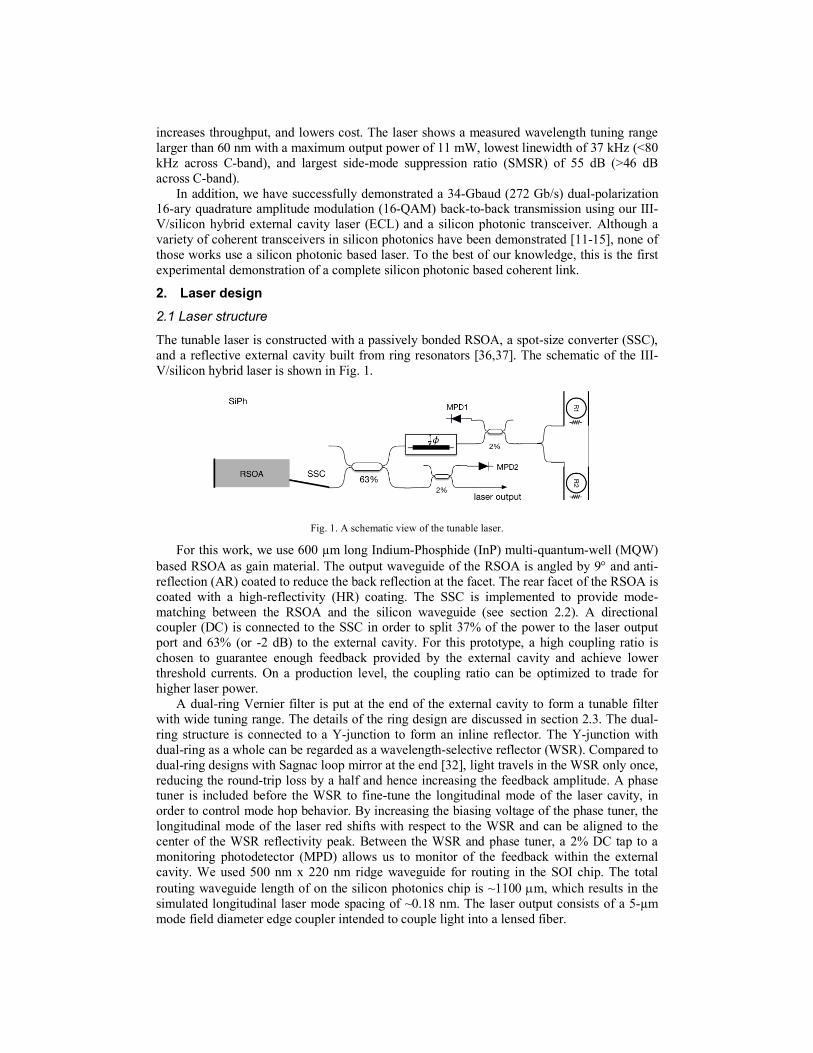
The tunable laser is constructed with a passively bonded RSOA, a spot-size converter (SSC), and a reflective external cavity built from ring resonators [36,37]. The schematic of the III-V/silicon hybrid laser is shown in Fig. 1.
Fig. 1. A schematic view of the tunable laser.
For this work, we use 600 µm long Indium-Phosphide (InP) multi-quantum-well (MQW) based RSOA as gain material. The output waveguide of the RSOA is angled by 9° and anti-reflection (AR) coated to reduce the back reflection at the facet. The rear facet of the RSOA is coated with a high-reflectivity (HR) coating. The SSC is implemented to provide mode-matching between the RSOA and the silicon waveguide (see section 2.2). A directional coupler (DC) is connected to the SSC in order to split 37% of the power to the laser output port and 63% (or -2 dB) to the external cavity. For this prototype, a high coupling ratio is chosen to guarantee enough feedback provided by the external cavity and achieve lower threshold currents. On a production level, the coupling ratio can be optimized to trade for higher laser power.
A dual-ring Vernier filter is put at the end of the external cavity to form a tunable filter with wide tuning range. The details of the ring design are discussed in section 2.3. The dual-ring structure is connected to a Y-junction to form an inline reflector. The Y-junction with dual-ring as a whole can be regarded as a wavelength-selective reflector (WSR). Compared to dual-ring designs with Sagnac loop mirror at the end [32], light travels in the WSR only once, reducing the round-trip loss by a half and hence increasing the feedback amplitude. A phase tuner is included before the WSR to fine-tune the longitudinal mode of the laser cavity, in order to control mode hop behavior. By increasing the biasing voltage of the phase tuner, the longitudinal mode of the laser red shifts with respect to the WSR and can be aligned to the center of the WSR reflectivity peak. Between the WSR and phase tuner, a 2% DC tap to a monitoring photodetector (MPD) allows us to monitor of the feedback within the external cavity. We used 500 nm x 220 nm ridge waveguide for routing in the SOI chip. The total routing waveguide length of on the silicon photonics chip is ~1100 µm, which results in the simulated longitudinal laser mode spacing of ~0.18 nm. The laser output consists of a 5-µm mode field diameter edge coupler intended to couple light into a lensed fiber.
2.2 Spot-size converter
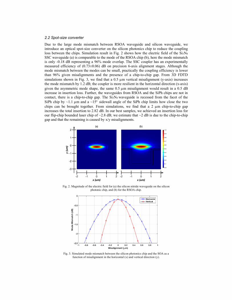
Due to the large mode mismatch between RSOA waveguide and silicon waveguide, we introduce an optical spot-size converter on the silicon photonics chip to reduce the coupling loss between the chips. Simulation result in Fig. 2 shows how the electric field of the Si3N4
SSC waveguide (a) is comparable to the mode of the RSOA chip (b), here the mode mismatch is only -0.18 dB representing a 96% mode overlap. The SSC coupler has an experimentally measured efficiency of (0.73±0.06) dB on precision 6-axis alignment stages. Although the mode mismatch between the modes can be small, practically the coupling efficiency is lower than 96% given misalignments and the presence of a chip-to-chip gap. From 3D FDTD simulations shown in Fig. 3, we find that a 0.5 µm vertical misalignment (y-axis) increases the mode mismatch by 1.2 dB; the coupler is more resilient in the horizontal direction (x-axis) given the asymmetric mode shape, the same 0.5 µm misalignment would result in a 0.5 dB increase in insertion loss. Further, the waveguides from RSOA and the SiPh chips are not in contact, there is a chip-to-chip gap. The Si3N4 waveguide is recessed from the facet of the SiPh chip by ~1.1 µm and a ~15° sidewall angle of the SiPh chip limits how close the two chips can be brought together. From simulations, we find that a 2 µm chip-to-chip gap increases the total insertion to 2.82 dB. In our best samples, we achieved an insertion loss for our flip-chip bounded laser chip of ~2.8 dB; we estimate that ~2 dB is due to the chip-to-chip gap and that the remaining is caused by x/y misalignments.
Fig. 2. Magnitude of the electric field for (a) the silicon nitride waveguide on the silicon
photonic chip, and (b) for the RSOA chip.
Fig. 3. Simulated mode mismatch between the silicon photonics chip and the SOA as a function of misalignment in the horizontal (x) and vertical direction (y).
2.3 External double-ring resonator laser cavity
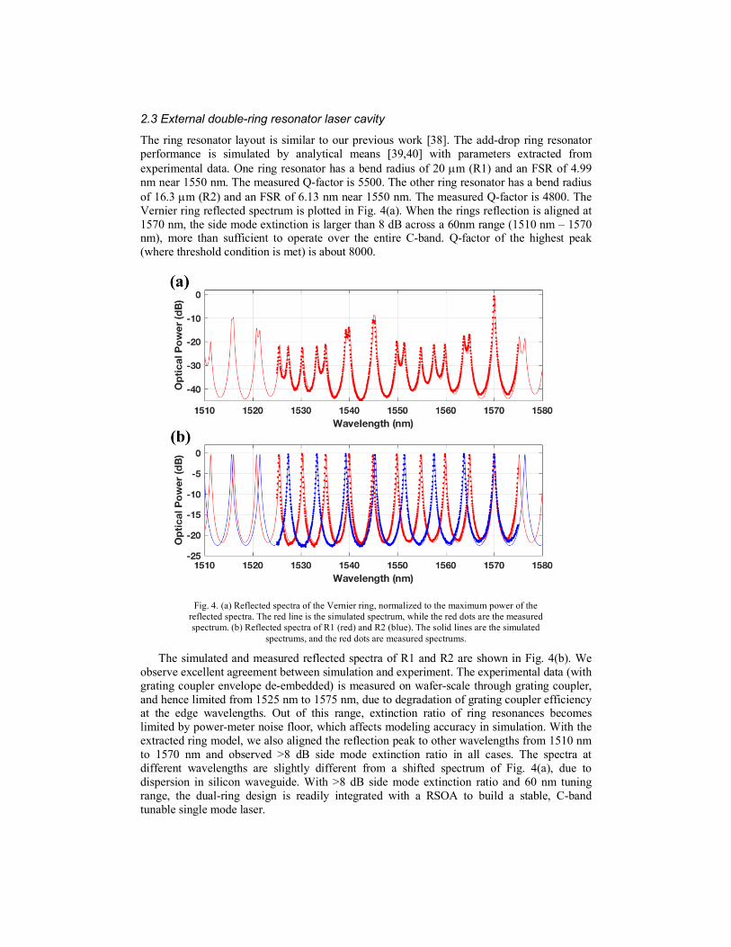
The ring resonator layout is similar to our previous work [38]. The add-drop ring resonator performance is simulated by analytical means [39,40] with parameters extracted from experimental data. One ring resonator has a bend radius of 20 µm (R1) and an FSR of 4.99 nm near 1550 nm. The measured Q-factor is 5500. The other ring resonator has a bend radius of 16.3 µm (R2) and an FSR of 6.13 nm near 1550 nm. The measured Q-factor is 4800. The Vernier ring reflected spectrum is plotted in Fig. 4(a). When the rings reflection is aligned at 1570 nm, the side mode extinction is larger than 8 dB across a 60nm range (1510 nm – 1570 nm), more than sufficient to operate over the entire C-band. Q-factor of the highest peak (where threshold condition is met) is about 8000.
Fig. 4. (a) Reflected spectra of the Vernier ring, normalized to the maximum power of the
reflected spectra. The red line is the simulated spectrum, while the red dots are the measured spectrum. (b) Reflected spectra of R1 (red) and R2 (blue). The solid lines are the simulated
spectrums, and the red dots are measured spectrums.
The simulated and measured reflected spectra of R1 and R2 are shown in Fig. 4(b). We observe excellent agreement between simulation and experiment. The experimental data (with grating coupler envelope de-embedded) is measured on wafer-scale through grating coupler, and hence limited from 1525 nm to 1575 nm, due to degradation of grating coupler efficiency at the edge wavelengths. Out of this range, extinction ratio of ring resonances becomes limited by power-meter noise floor, which affects modeling accuracy in simulation. With the extracted ring model, we also aligned the reflection peak to other wavelengths from 1510 nm to 1570 nm and observed >8 dB side mode extinction ratio in all cases. The spectra at different wavelengths are slightly different from a shifted spectrum of Fig. 4(a), due to dispersion in silicon waveguide. With >8 dB side mode extinction ratio and 60 nm tuning range, the dual-ring design is readily integrated with a RSOA to build a stable, C-band tunable single mode laser.
3. Laser fabrication and integration The silicon photonic chip was fabricated at a complementary metal-oxide-semiconductor (CMOS) foundry using standard CMOS-compatible processes. The substrate is an SOI wafer with a 220-nm device layer. Front end etching and doping processes are used to build the waveguides and active components. A pit is formed with hard-stop structures embedded, in order to aid in aligning the silicon photonics chip with the III-V device.
The InP RSOA chip was built in a III-V foundry using standard III-V processing techniques. The substrate was a 100 mm InP wafer with an epitaxial grown 1.9 µm wide ridge waveguide layer. The MQW layer was built using five AlGaInAs quantum wells with a gain spectrum centered in the C-Band at operating temperatures. The optical mode was roughly centered in the quantum well region which was located directly under the ridge. The extracted waveguide loss for RSOA is 12 1/cm. A series of etches defined the hard stop at the MQW layer as well as a recessed gold contact pad for bonding with the locations of these features matching that of the silicon photonic chip. The InP wafer was cleaved into bars which were HR coated on the back facet and anti-reflection coated on the front facet. AR facet was coated to 1.45 to match the effective index of the mode in the silicon photonics and of the index matching gel making a pair of low reflection interfaces. The bars were then cleaved into chips comprising two channels each.
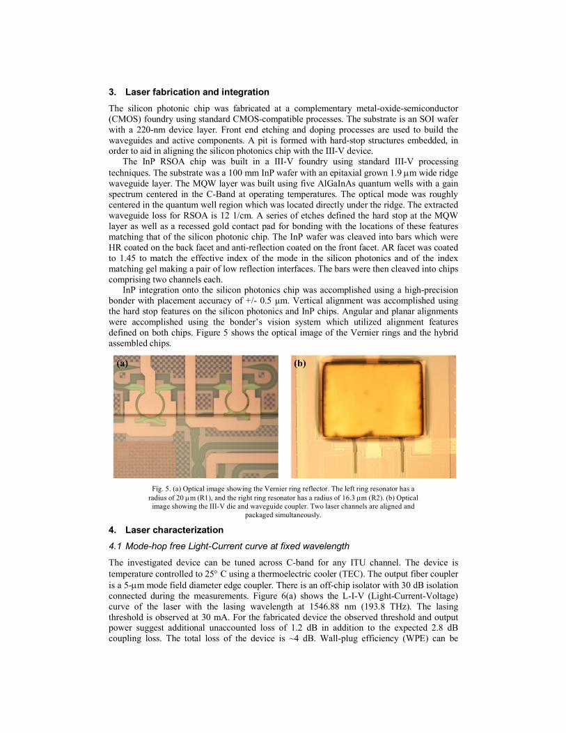
InP integration onto the silicon photonics chip was accomplished using a high-precision bonder with placement accuracy of +/- 0.5 µm. Vertical alignment was accomplished using the hard stop features on the silicon photonics and InP chips. Angular and planar alignments were accomplished using the bonder’s vision system which utilized alignment features defined on both chips. Figure 5 shows the optical image of the Vernier rings and the hybrid assembled chips.
Fig. 5. (a) Optical image showing the Vernier ring reflector. The left ring resonator has a
radius of 20 µm (R1), and the right ring resonator has a radius of 16.3 µm (R2). (b) Optical image showing the III-V die and waveguide coupler. Two laser channels are aligned and
packaged simultaneously.
4. Laser characterization 4.1 Mode-hop free Light-Current curve at fixed wavelength
The investigated device can be tuned across C-band for any ITU channel. The device is temperature controlled to 25° C using a thermoelectric cooler (TEC). The output fiber coupler is a 5-µm mode field diameter edge coupler. There is an off-chip isolator with 30 dB isolation connected during the measurements. Figure 6(a) shows the L-I-V (Light-Current-Voltage) curve of the laser with the lasing wavelength at 1546.88 nm (193.8 THz). The lasing threshold is observed at 30 mA. For the fabricated device the observed threshold and output power suggest additional unaccounted loss of 1.2 dB in addition to the expected 2.8 dB coupling loss. The total loss of the device is ~4 dB. Wall-plug efficiency (WPE) can be
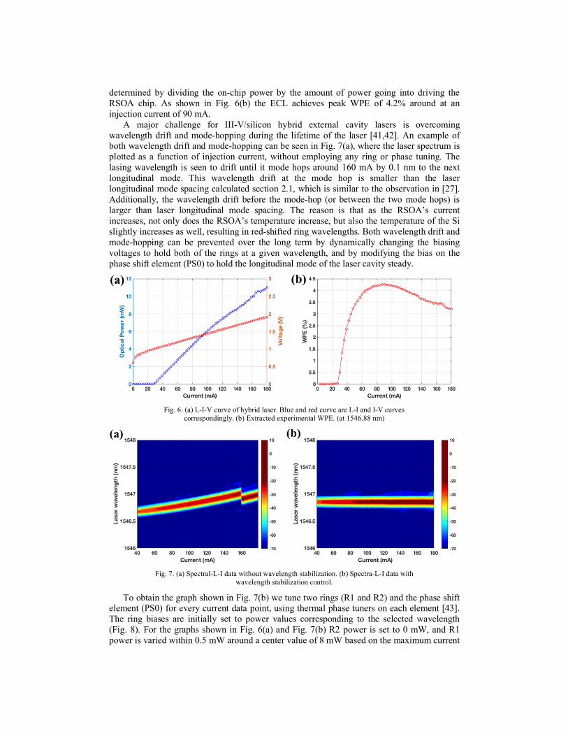
determined by dividing the on-chip power by the amount of power going into driving the RSOA chip. As shown in Fig. 6(b) the ECL achieves peak WPE of 4.2% around at an injection current of 90 mA.
A major challenge for III-V/silicon hybrid external cavity lasers is overcoming wavelength drift and mode-hopping during the lifetime of the laser [41,42]. An example of both wavelength drift and mode-hopping can be seen in Fig. 7(a), where the laser spectrum is plotted as a function of injection current, without employing any ring or phase tuning. The lasing wavelength is seen to drift until it mode hops around 160 mA by 0.1 nm to the next longitudinal mode. This wavelength drift at the mode hop is smaller than the laser longitudinal mode spacing calculated section 2.1, which is similar to the observation in [27]. Additionally, the wavelength drift before the mode-hop (or between the two mode hops) is larger than laser longitudinal mode spacing. The reason is that as the RSOA’s current increases, not only does the RSOA’s temperature increase, but also the temperature of the Si slightly increases as well, resulting in red-shifted ring wavelengths. Both wavelength drift and mode-hopping can be prevented over the long term by dynamically changing the biasing voltages to hold both of the rings at a given wavelength, and by modifying the bias on the phase shift element (PS0) to hold the longitudinal mode of the laser cavity steady.
Fig. 6. (a) L-I-V curve of hybrid laser. Blue and red curve are L-I and I-V curves correspondingly. (b) Extracted experimental WPE. (at 1546.88 nm)
Fig. 7. (a) Spectral-L-I data without wavelength stabilization. (b) Spectra-L-I data with wavelength stabilization control.
To obtain the graph shown in Fig. 7(b) we tune two rings (R1 and R2) and the phase shift element (PS0) for every current data point, using thermal phase tuners on each element [43]. The ring biases are initially set to power values corresponding to the selected wavelength (Fig. 8). For the graphs shown in Fig. 6(a) and Fig. 7(b) R2 power is set to 0 mW, and R1 power is varied within 0.5 mW around a center value of 8 mW based on the maximum current

reading from the MPD. This corresponds to a lasing wavelength of 1546.88 nm. The phase tuner is initially set to a value corresponding to maximum reading on the MPD. Aligning the rings as described result in maximum reflectivity and hence maximum power on the MPD. The rings are hence aligned with each other by maximizing the photocurrent reading on the MPD. The laser cavity phase tuner is then scanned and set to a value that biases the laser longitudinal mode to the center double ring resonance [43]. This way we keep the lasing mode away from mode-hop regions. However, tuning the phase tuner might cause the lasing wavelength to drift, consequently requiring further adjustment of the ring biases. This procedure is iteratively repeated until the measured wavelength matches the target wavelength. For this procedure, we use an optical spectrum analyzer (OSA) to monitor the lasing wavelength as the injection current is increased. This method allows us to tune and maintain the lasing peak around the desired wavelength to within OSA’s resolution of 0.02 nm for every injection current, corresponding to tuning accuracy of +/- 1.25 GHz in frequency. Such accuracy is within the tolerance needed in most communications applications (+/- 2.5 GHz) [44]. This procedure is employed to demonstrate a mode-hop and wavelength-drift free operation as shown in Fig. 7(b) and ensure ITU-compliant operation away from mode-hop points. Further work is needed to ensure that wavelength is continuously stabilized during the laser operation.
4.2 Tunability
Figure 8 shows the lasing wavelengths under different thermal tuning power applied to the ring resonators with RSOA drive current of 180 mA. For every data the phase tuner was scanned between the first and second π shift and optimized to a center maximum. This ensures operation away from mode-hop regions. Single-wavelength lasing with a SMSR in excess of 46 dB was obtained across a 60-nm tuning range. The tuning range covers the entire telecommunication C-band. The color plot shows the laser tunability from 1515 nm to 1575 nm. The hue gradient along the diagonal color lines shows that the wavelength can be continuously tuned. Each one of the diamonds overlaid on the color plot represents the wavelength for an ITU channel in a 100 GHz ITU grid across the entire C-band. Figure 9 also shows that the tuning range of the laser covers the entire C-band.
Fig. 8. Lasing wavelength under different R1 and R2 basing powers. The diamond markers indicate the basing powers at different ITU grid.

Fig. 9. Measured lasing spectra of the tunable laser across the C-band.
4.3 Spectral performance (SMSR and linewidth)
The SMSR was measured using an OSA with a resolution of 0.02 nm at room temperature, with a drive current of 180 mA. The highest measured SMSR was 55 dB, as indicated in Fig. 10(a). Figure 10(b) shows the measured SMSR at different wavelengths according to the C-band 100-GHz spacing dense wavelength division multiplexing (DWDM) ITU grid. The measured SMSR is larger than 46 dB from 1525 nm to 1575 nm, being smaller at the edges of the gain bandwidth.
Fig. 10. (a) Measured laser output power spectrum with the highest SMSR of 55 dB. (b) Measured SMSR at C-band, 100-GHz-spacing DWDM ITU grid. (c) FM-noise spectrum using
heterodyne laser linewidth measurement method at 1553 nm. (d) Measured linewidth at different wavelengths across the C-band.
The linewidth of the laser cannot be determined from the spectrum in Fig. 10(a), because the laser linewidth is smaller than the resolution of the OSA. To measure the linewidth, we adopt a heterodyne measurement method [24,45]. The output from our laser was mixed with a tunable laser (Keysight N7711A) and passed through a coherent receiver. The electrical signal is then observed on a real-time scope. The combined linewidth is analyzed from the FM noise spectrum, by taking the average of the flat region of the noise spectrum (between 20 MHz and 80 MHz) and multiplying by π [45]. The linewidth integration time of our measurement can be calculated to be 25 µs. Our linewidth integration time was set properly to measure the entire FM-noise spectrum, especially the bottom flat region of the FM-noise spectrum (where we extracted the linewidth). The intrinsic linewidth of the reference Keysight laser was measured using the same method (~40 kHz). The intrinsic linewidth of our ECL laser can be obtained by subtracting linewidth of the reference laser from the combined value. The measured linewidth for the ECL is below 80 kHz for 7 wavelengths selected as samples across the C-band as shown in Fig. 10(d). As a complimentary measurement to the linewidth we have also measured the relative-intensity-noise (RIN) of our laser at various wavelength using a Sycatus RIN measurement system. We have the determined that for wavelengths in the C-band the maximal RIN in a frequency range from 100 MHz to 13 GHz was better than – 135 dB/Hz. Due to the limited sensitivity of the system values lower than -135 dB/Hz cannot be measured.
5. Coherent transmission 5.1 Experimental setup
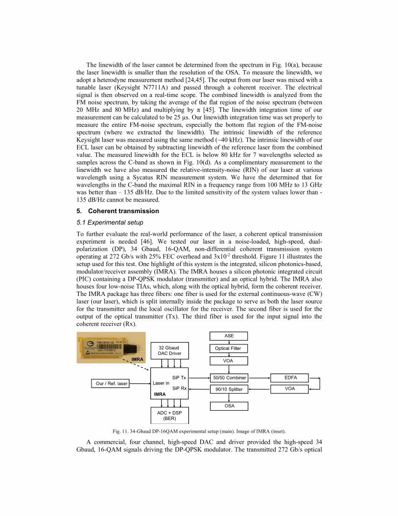
To further evaluate the real-world performance of the laser, a coherent optical transmission experiment is needed [46]. We tested our laser in a noise-loaded, high-speed, dual-polarization (DP), 34 Gbaud, 16-QAM, non-differential coherent transmission system operating at 272 Gb/s with 25% FEC overhead and 3x10⁻² threshold. Figure 11 illustrates the setup used for this test. One highlight of this system is the integrated, silicon photonics-based, modulator/receiver assembly (IMRA). The IMRA houses a silicon photonic integrated circuit (PIC) containing a DP-QPSK modulator (transmitter) and an optical hybrid. The IMRA also houses four low-noise TIAs, which, along with the optical hybrid, form the coherent receiver. The IMRA package has three fibers: one fiber is used for the external continuous-wave (CW) laser (our laser), which is split internally inside the package to serve as both the laser source for the transmitter and the local oscillator for the receiver. The second fiber is used for the output of the optical transmitter (Tx). The third fiber is used for the input signal into the coherent receiver (Rx).
Fig. 11. 34-Gbaud DP-16QAM experimental setup (main). Image of IMRA (inset).
A commercial, four channel, high-speed DAC and driver provided the high-speed 34 Gbaud, 16-QAM signals driving the DP-QPSK modulator. The transmitted 272 Gb/s optical

signal was noise-loaded and looped back into the Rx signal port of the IMRA. A commercial high-speed ADC and DSP were used to digitize and process the output signals from the IMRA receiver and measure the bit-error-rate (BER) performance of the system. The noise-loading setup (ASE source, optical filter, and variable optical attenuator (VOA)) allowed us to control the optical signal-to-noise ratio (OSNR). An erbium-doped fiber amplifier (EDFA) and VOA were placed at the Tx output to boost and control the optical power into the receiver. An optical spectrum analyzer measured the signal power and OSNR into the receiver. With this setup, we can measure BER vs OSNR performance of the transmission system. Our tests were performed in loopback (back to back) mode. This configuration provided a simple way to test whether the DSP can handle the linewidth of the laser source. We note that in coherent transmission systems, the section of the DSP which handles the laser linewidth is separate from the section of the DSP section which handles fiber dispersion. Therefore, for this particular test, we chose not to propagate the Tx signal over long lengths of fiber.
5.2 Experimental results of 34-Gbaud 16-QAM transmission
In order to assess the performance of our laser source in the coherent system, we made two measurements. First, a reference measurement was made with a commercial tunable laser source (Santur ITLA) suitable for long-haul coherent systems. The CW laser power was 16 dBm. The laser wavelength was 1547.2 nm. The optical signal power into the receiver was -10 dBm. This first measurement provided a baseline OSNR vs BER curve at -10 dBm input into the receiver. For the second measurement, the commercial laser was replaced with our laser source (this work). An EDFA was used to boost the output from our laser to 16 dBm.
Figure 12 shows the comparison between the OSNR vs. BER curves measured at 1547.2 nm with both the commercial laser and our laser (this work). No noticeable shift was observed between the two curves, and no uncorrected errors were detected up to the FEC threshold. Similar results were obtained with a slightly different setup, in which we compared our laser against the reference laser as source for a noise-loaded, LiNbO3-based, 16-QAM, 272 Gb/s transmitter looped back into our SiPh Rx, but using a commercial laser (ITLA) as the local oscillator.
Fig. 12. Measured BER vs. OSNR at 1547.2 nm.
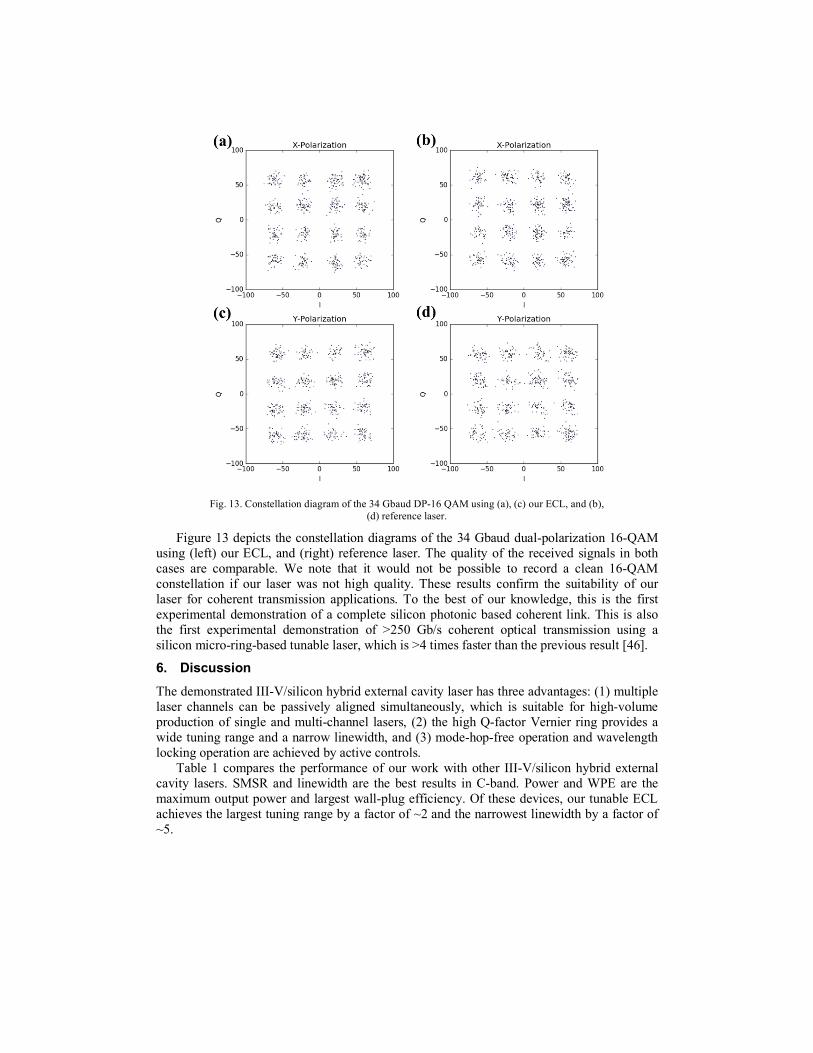
Fig. 13. Constellation diagram of the 34 Gbaud DP-16 QAM using (a), (c) our ECL, and (b),
(d) reference laser.
Figure 13 depicts the constellation diagrams of the 34 Gbaud dual-polarization 16-QAM using (left) our ECL, and (right) reference laser. The quality of the received signals in both cases are comparable. We note that it would not be possible to record a clean 16-QAM constellation if our laser was not high quality. These results confirm the suitability of our laser for coherent transmission applications. To the best of our knowledge, this is the first experimental demonstration of a complete silicon photonic based coherent link. This is also the first experimental demonstration of >250 Gb/s coherent optical transmission using a silicon micro-ring-based tunable laser, which is >4 times faster than the previous result [46].
6. Discussion The demonstrated III-V/silicon hybrid external cavity laser has three advantages: (1) multiple laser channels can be passively aligned simultaneously, which is suitable for high-volume production of single and multi-channel lasers, (2) the high Q-factor Vernier ring provides a wide tuning range and a narrow linewidth, and (3) mode-hop-free operation and wavelength locking operation are achieved by active controls.
Table 1 compares the performance of our work with other III-V/silicon hybrid external cavity lasers. SMSR and linewidth are the best results in C-band. Power and WPE are the maximum output power and largest wall-plug efficiency. Of these devices, our tunable ECL achieves the largest tuning range by a factor of ~2 and the narrowest linewidth by a factor of ~5.

Table 1. Performance comparison of recent C-band tunable laser works
Property [27] (2012)
[28] (2012)
[24] (2013)
[22] (2013)
[23] (2013)
[33] (2014)
This work (2018)
Integration Hybrid Hybrid Heterogeneous
Heterogeneous
Heterogeneous
Hybrid Hybrid
Alignment Active Passive Passive Passive Passive Active Passive
Coupling Butt Butt Butt Vertical Vertical Butt Butt
Laser Type DBR Single Ring + DBR
DBR Single Ring + DBR
Vernier Ring
Vernier Ring
Vernier Ring
Tuning Range(nm)
8 N.A. >20 8 >40 35 >60
Power (mW)
6 15 8 10 3.3 20 11
WPE (%) 9.5 7.6 N.A. N.A. N.A. 7.8 4.2
SMSR(dB) 45 40 40 50 45 40 55
Linewidth (kHz)
N.A. N.A. 200 1700 338 27000 37
7. Conclusion We demonstrate a III-V/silicon hybrid external cavity laser with a tuning range larger than 60 nm around the C-band on a silicon-on-insulator platform. A III-V semiconductor gain chip is embedded in the silicon chip and is edge-coupled into the silicon chip. The demonstrated packaging method requires only passive alignment and thus potentially suitable for mass production. The laser has a largest output power of 11 mW with a maximum WPE of 4.2%. and a SMSR as large as 55 dB. The measured linewidth is as narrow as 37 kHz, which is the narrowest linewidth using a silicon-based (not silicon nitride-based) external cavity. In addition, we demonstrate successfully a 34 Gbaud DP-16 QAM transmission using our laser and a silicon photonic transceiver on par with the performance of commercially available lasers. To the best of our knowledge, this is the first experimental demonstration of a complete silicon photonic based coherent link. This is also the first experimental demonstration of >250 Gb/s coherent optical transmission using a silicon micro-ring based tunable laser, which is the fastest coherent optical transmission speed using a silicon micro-ring based tunable laser.


![arXiv:1610.05877v1 [physics.ins-det] 19 Oct 2016Widely tunable, narrow linewidth external-cavity gain chip laser for spectroscopy between 1.0 - 1.1 m D ONG K. S HIN,* B RYCE M. H ENSON,](https://cdn.vdocuments.mx/doc/165x107/5faf7ee5b0de1a7e916c884e/arxiv161005877v1-19-oct-2016-widely-tunable-narrow-linewidth-external-cavity.jpg)


