UNIVERSITÀ DEGLI STUDI DI NAPOLI FEDERICO II
DOTTORATO DI RICERCA IN INGEGNERIA ELETTRICA XXI CICLO
A Fast Digital Integrator for magnetic measurements
Relatori Candidato Ch.mo Prof. Nello POLESE Giovanni SPIEZIA Ch.mo Prof. Pasquale ARPAIA Co-relatore Dott. Luca BOTTURA Coordinatore Ch.mo Prof. Guido CARPINELLI
Anno accademico 2008

To my parents

Acknowledgments
I would like to thank my supervisor Prof. Pasquale Arpaia for his full-time
guide. His enthusiasm encouraged me a lot by providing a strong motivation
to do well my work during the thesis work as a whole.
I would like to express also my gratitude to Luca Bottura, my CERN
supervisor, who launched the FDI project. Our discussions were always prone
of clever suggestions.
I would like to acknowledge Louis Walckiers and Marco Buzio for their
help and participation to the project.
I would like to express my appreciation to my tutor from the university
of Naples, Prof. Nello Polese. His guide, helpfulness, and patience were
important to achieve this final result.
I would like to acknowledge also the coordinators of the doctoral school
from Naples, Prof. Giovanni Miano and Prof. Guido Carpinelli for their
careful guide during my work.
I would like to express my gratitude to Prof. Felice Cennamo. He is a
wise guide and a wonderful person who always helped me with his precious
suggestions.
I would like to thank Alessandro Masi sincerely, who believed in me after
my stage at CERN and introduced me to Prof. Arpaia and to the AT/MTM
i

Acknowledgments
group to start this project.
My gratitude also goes to Walter Scandale for the trust he had in me,
from our first meeting at CERN.
I would like to acknowledge Stefano Redaelli who always gave me precious
advices. A special thanks also goes to Tatiana Pieloni.
I would like to acknowledge my colleagues from the the university of
Naples too, for their help in academic activities.
My work is a part of a project that involved the work of many persons.
I would like to express my gratitude to David Giloteaux for his fundamental
contribution to the development of the FDI card. I learnt a lot from his
experience in electronics.
I would like to thank Vitaliano Inglese. We worked together since I came
in the AT department. I found in him a good desk-mate and above all a
great friend.
I had the opportunity to work with consultants from University of Sannio.
I would like to thank Pasquale Cimmino, to work with him was helpful and
amusing. A special thanks also goes to Prof. Giuseppe Di Lucca, MarioLuca
Bernardi, and Giuseppe La Commara, for the useful collaboration.
I would like to thank Domenico Della Ratta, Stefano Tiso, Giancarlo Gol-
luccio, Giuseppe Montenero, and Ernesto De Matteis. We had a good time
together and their final works for the master degree were a great contribution
to the project.
A special thank also goes to Laurent Deniau, J. Garcia Perez, and Peter
Galbraith from CERN, and Nathan Brooks, from the university of Texas, for
their precious help.
I would like to thank mon amie urbaine Saskia. A very special thanks
ii

Acknowledgments
also goes to Pierpaolo and Isabella. I cannot make a list of all my friends,
because I am afraid to forget someone. Then, I take up the suggestion of my
grandmother and I express my gratitude to all of them.
Last but not least, I would like to say grazie to my father Giuseppe, my
mother Concetta, and my little-big brother Onofrio who supported me by
showing their deep and unconditioned affect, the most precious contribution
for my work.
iii
Contents
Summary 1
Introduction 3
1 CERN context of magnetic measurements 10
1.1 CERN accelerators . . . . . . . . . . . . . . . . . . . . . . . . 10
1.2 The Large Hadron Collider . . . . . . . . . . . . . . . . . . . . 12
1.3 LHC superconducting magnets . . . . . . . . . . . . . . . . . . 15
1.3.1 Dipole Magnets . . . . . . . . . . . . . . . . . . . . . . 15
2 State of the art of magnetic field measurements 19
2.1 Methods and instrumentation . . . . . . . . . . . . . . . . . . 20
2.1.1 Rotating coils . . . . . . . . . . . . . . . . . . . . . . . 22
2.1.2 Stretched wire . . . . . . . . . . . . . . . . . . . . . . . 25
2.1.3 Magnetic resonance techniques . . . . . . . . . . . . . . 26
2.1.4 Hall probes . . . . . . . . . . . . . . . . . . . . . . . . 27
2.1.5 Fluxgate magnetometer . . . . . . . . . . . . . . . . . 28
2.1.6 Miscellanea . . . . . . . . . . . . . . . . . . . . . . . . 29
2.2 Digital integrators . . . . . . . . . . . . . . . . . . . . . . . . . 29
2.2.1 Portable Digital Integrator . . . . . . . . . . . . . . . . 29
2.2.2 Technologies from other research centers . . . . . . . . 31
2.2.3 Commercial integrators and rationale for a custom so-
lution . . . . . . . . . . . . . . . . . . . . . . . . . . . 32
3 Instrument requirements and main issues for fast magnetic
measurements 34
3.1 Analysis of the rotating coil method . . . . . . . . . . . . . . . 34
iv
CONTENTS
3.2 Frequency bandwidth . . . . . . . . . . . . . . . . . . . . . . . 36
3.3 Resolution, accuracy, and harmonic distortion . . . . . . . . . 37
3.4 Gain and offset stability . . . . . . . . . . . . . . . . . . . . . 39
4 Conceptual design 41
4.1 Proposal . . . . . . . . . . . . . . . . . . . . . . . . . . . . . . 41
4.2 Working principle and key design concepts . . . . . . . . . . . 43
4.3 The architecture . . . . . . . . . . . . . . . . . . . . . . . . . 45
4.4 Measurement algorithm . . . . . . . . . . . . . . . . . . . . . 46
5 Metrological analysis 48
5.1 Analytical study . . . . . . . . . . . . . . . . . . . . . . . . . 49
5.1.1 Time-domain uncertainty . . . . . . . . . . . . . . . . 49
5.1.2 Amplitude-domain uncertainty . . . . . . . . . . . . . 50
5.2 Preliminary numerical analysis . . . . . . . . . . . . . . . . . . 52
5.2.1 Integration algorithm and ADC rate . . . . . . . . . . 54
5.2.2 UTC . . . . . . . . . . . . . . . . . . . . . . . . . . . . 55
5.2.3 Time-domain uncertainty effects . . . . . . . . . . . . . 55
5.2.4 Amplitude-domain uncertainty effects . . . . . . . . . . 57
5.3 Comprehensive numerical analysis . . . . . . . . . . . . . . . . 60
5.3.1 Generic analysis strategy . . . . . . . . . . . . . . . . . 61
5.3.2 Application to FDI . . . . . . . . . . . . . . . . . . . . 66
5.4 Discussion . . . . . . . . . . . . . . . . . . . . . . . . . . . . . 76
6 Physical design and implementation 78
6.1 The front-end panel . . . . . . . . . . . . . . . . . . . . . . . . 78
6.2 The digitizer chain . . . . . . . . . . . . . . . . . . . . . . . . 80
6.2.1 PGA: AD625 . . . . . . . . . . . . . . . . . . . . . . . 81
6.2.2 ADC: AD7634 . . . . . . . . . . . . . . . . . . . . . . . 82
6.3 DSP: Shark 21262 . . . . . . . . . . . . . . . . . . . . . . . . . 85
6.4 FPGA: Spartan XC3S1000L . . . . . . . . . . . . . . . . . . . 87
6.4.1 The UTC implementation . . . . . . . . . . . . . . . . 88
6.4.2 Offset and gain correction . . . . . . . . . . . . . . . . 89
6.5 The PXI communication bus . . . . . . . . . . . . . . . . . . . 90
6.6 FDI firmware . . . . . . . . . . . . . . . . . . . . . . . . . . . 91
v
CONTENTS
6.6.1 On-line measurement algorithm . . . . . . . . . . . . . 94
6.7 FDI software . . . . . . . . . . . . . . . . . . . . . . . . . . . 97
6.7.1 Flexible Framework for Magnetic Measurements . . . . 97
6.7.2 FDI classes . . . . . . . . . . . . . . . . . . . . . . . . 102
7 Metrological and throughput rate characterization 105
7.1 Metrological characterization . . . . . . . . . . . . . . . . . . . 106
7.1.1 Measurement station and characterization strategy . . 106
7.1.2 Static tests . . . . . . . . . . . . . . . . . . . . . . . . 107
7.1.3 Dynamic tests . . . . . . . . . . . . . . . . . . . . . . . 111
7.1.4 Time base tests . . . . . . . . . . . . . . . . . . . . . . 114
7.2 Throughput rate characterization . . . . . . . . . . . . . . . . 116
7.2.1 Test procedure . . . . . . . . . . . . . . . . . . . . . . 117
7.2.2 Results . . . . . . . . . . . . . . . . . . . . . . . . . . . 118
7.3 FDI specifications . . . . . . . . . . . . . . . . . . . . . . . . . 122
8 On-field test on superconducting magnets 123
8.1 The test plan . . . . . . . . . . . . . . . . . . . . . . . . . . . 123
8.1.1 The measurement method . . . . . . . . . . . . . . . . 124
8.1.2 The measurement station . . . . . . . . . . . . . . . . 127
8.1.3 The validation procedure . . . . . . . . . . . . . . . . . 128
8.1.4 The characterization procedure . . . . . . . . . . . . . 129
8.2 Experimental results . . . . . . . . . . . . . . . . . . . . . . . 131
Conclusions 139
References 143
vi

List of Figures
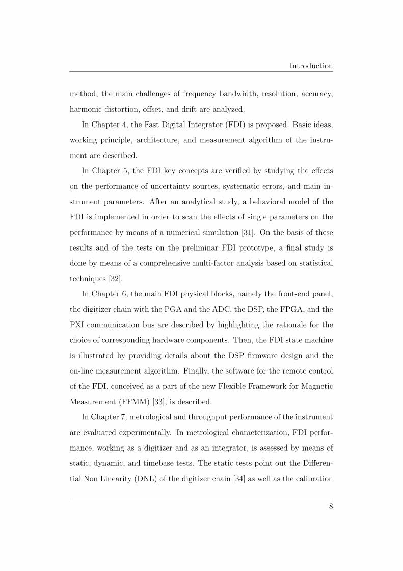
1.1 The accelerator chain at CERN (PS, SPS, and the Large Hadron Collider)
and further experimental area (CNGS and AD). . . . . . . . . . . . . 11
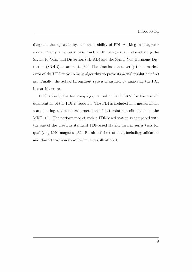
1.2 Overview of the Geneva area with a drawn of the two circular acceler-
ators: Super Proton Synchrotron (SPS 7 Km) and the Large Hadron
Collider (LHC 27 Km). . . . . . . . . . . . . . . . . . . . . . . . . 12
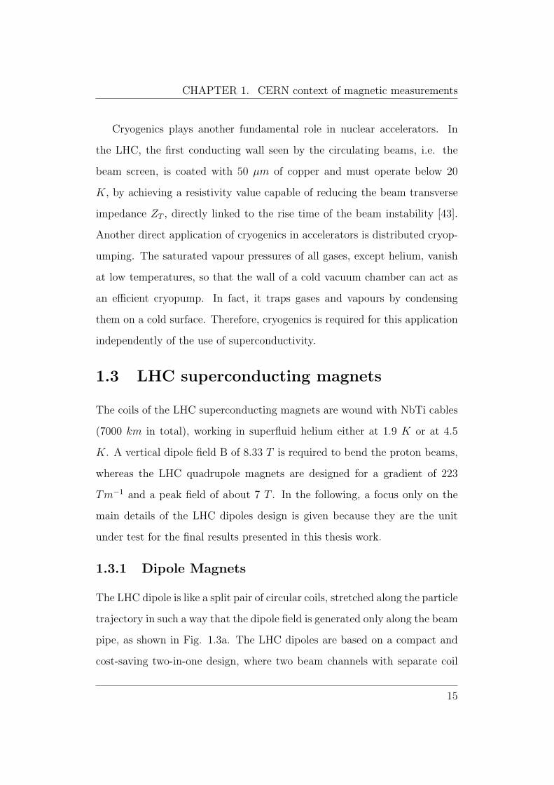
1.3 The 15-m long LHC superconducting dipole: a) Magnetic field; b) par-
ticulars. . . . . . . . . . . . . . . . . . . . . . . . . . . . . . . . 16
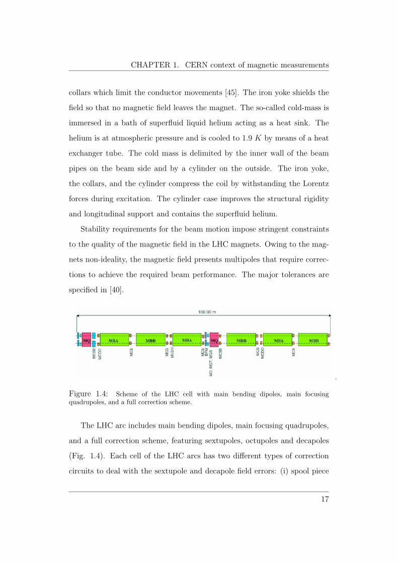
1.4 Scheme of the LHC cell with main bending dipoles, main focusing quadrupoles,
and a full correction scheme. . . . . . . . . . . . . . . . . . . . . . 17
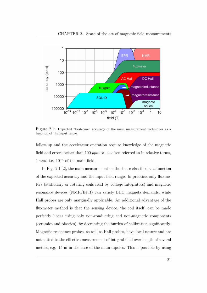
2.1 Expected ”best-case” accuracy of the main measurement techniques as a
function of the input range. . . . . . . . . . . . . . . . . . . . . . . 21
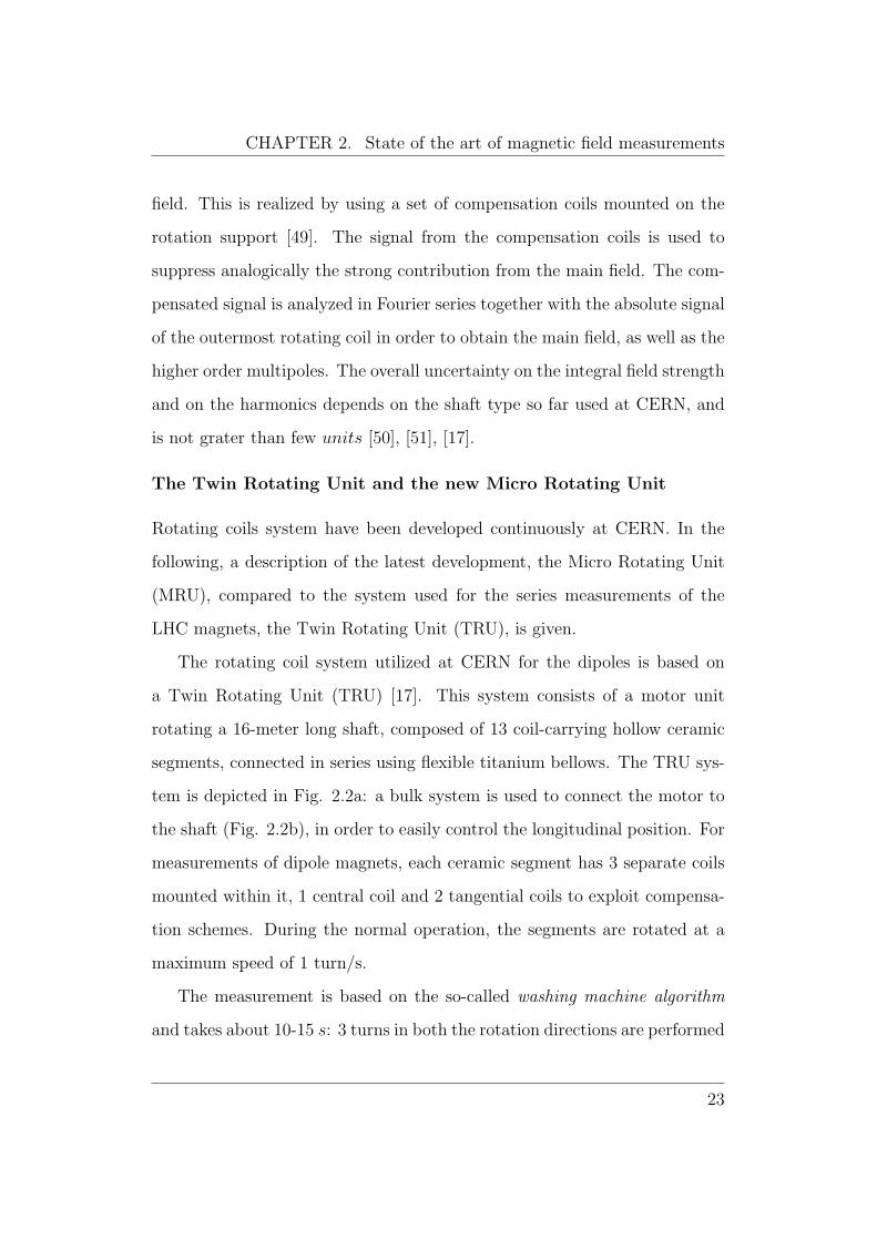
2.2 The TRU unit (a) is attached to the magnet anticryostat by means of a
bulk system (b). . . . . . . . . . . . . . . . . . . . . . . . . . . . 24
2.3 The MRU unit (a) is attached directly to the magnet anticryostat(b). . . 25
3.1 Comparison between TRU- (2) and MRU- (◦) based systems: flux reso-
lution as a function of the integration time. . . . . . . . . . . . . . . 38
3.2 Comparison between TRU- (2) and MRU- (◦, �) based systems: SNR as
a function of the integration time. . . . . . . . . . . . . . . . . . . . 40
4.1 Theoretical performance limits of state-of-art instruments and FDI com-
pared to working areas of old and new generations of rotating coils. . . . 42
4.2 FDI working principle. . . . . . . . . . . . . . . . . . . . . . . . . 43
4.3 FDI conceptual architecture. . . . . . . . . . . . . . . . . . . . . . 46
4.4 Rectangular algorithm. . . . . . . . . . . . . . . . . . . . . . . . . 47
4.5 Time diagram of the FDI measurement. . . . . . . . . . . . . . . . . 47
vii
LIST OF FIGURES
5.1 Influence on FDI performance of algorithm type, ADC sampling rate,
and flux sampling rate. . . . . . . . . . . . . . . . . . . . . . . . . 54
5.2 UTC influence on FDI performance: RMS error for (a) rectangular algo-
rithm and (b) trapezoidal algorithm. . . . . . . . . . . . . . . . . . 56
5.3 Statistical average of the flux uncertainty as function of the UTC jitter. . 57
5.4 Influence of the time-domain uncertainty on the flux uncertainty . . . . 58
5.5 Flux uncertainty as function of the time. . . . . . . . . . . . . . . . 58
5.6 Statistical average of the flux uncertainty as function of the signal input
noise. . . . . . . . . . . . . . . . . . . . . . . . . . . . . . . . . 59
5.7 Procedure for statistical-based analysis. . . . . . . . . . . . . . . . . 63
5.8 FDI model. . . . . . . . . . . . . . . . . . . . . . . . . . . . . . 68
5.9 Pareto log plot of parameter’s variance ratios (DF: degree of freedom). . 72
5.10 Plots of ANOVA model standardized residuals: (a) scatter, and (b) nor-
mal probability. . . . . . . . . . . . . . . . . . . . . . . . . . . . 73
5.11 Comparison between metamodel, MonteCarlo simulation, and Kim’s model. 75
5.12 Comparison among simulated performance (2), experimental performance
(�), and metamodel predictions (o). . . . . . . . . . . . . . . . . . . 75
6.1 The FDI board. . . . . . . . . . . . . . . . . . . . . . . . . . . . 79
6.2 FDI front-end panel. . . . . . . . . . . . . . . . . . . . . . . . . . 80
6.3 FDI instrumentation amplifier. . . . . . . . . . . . . . . . . . . . . 81
6.4 Resistor network structure of the FDI instrumentation amplifier. . . . . 83
6.5 Differential and bipolar input legs of the ADC. . . . . . . . . . . . . 84
6.6 Buffer circuit to delete the common mode voltage. . . . . . . . . . . . 85
6.7 UTC implementation. . . . . . . . . . . . . . . . . . . . . . . . . 88
6.8 Architecture of the PXI-based communication system of the FDI. . . . . 91
6.9 The FDI state machine. . . . . . . . . . . . . . . . . . . . . . . . 92
6.10 Trapezoidal algorithm. . . . . . . . . . . . . . . . . . . . . . . . . 96
6.11 Evaluation of τbkand τak+1 by means of the UTC. . . . . . . . . . . . 97
6.12 FFMM conceptual architecture. . . . . . . . . . . . . . . . . . . . . 100
6.13 Architecture of the Scheme: class diagram. . . . . . . . . . . . . . . 101
6.14 FDI data transfer. . . . . . . . . . . . . . . . . . . . . . . . . . . 103
7.1 DNL of PDI in 7 different regions of the input range: mean and standard
deviation for each transition level group. . . . . . . . . . . . . . . . . 108
viii
LIST OF FIGURES
7.2 DNL of FDI in 7 different regions of the input range: mean and standard
deviation for each transition level group. . . . . . . . . . . . . . . . . 109
7.3 FDI static nonlinearity errors (o) and 2σ-uncertainty bands (+), relative
to full-scale. . . . . . . . . . . . . . . . . . . . . . . . . . . . . . 110
7.4 FDI 24-hours 2σ-stability bands (o) and 2σ-repeatability bands (over 30
minutes) (+), relative to full scale. . . . . . . . . . . . . . . . . . . 111
7.5 Comparison of FFT computed by applying different windowing functions. 113
7.6 FFT of the signal integrated by the FDI. . . . . . . . . . . . . . . . 114
7.7 FDI (◦) and PDI (4) dynamic performance vs. oversampling ratio, as
digitizers (left) and as integrators (right). . . . . . . . . . . . . . . . 115
7.8 The time interval counter (a) and the τa (b) values evaluated by the
32-bit integer algorithm. . . . . . . . . . . . . . . . . . . . . . . . 116
7.9 The PXI initiator-target chain of the FDI. . . . . . . . . . . . . . . . 117
7.10 PCI signals for a single read operation. . . . . . . . . . . . . . . . . 118
7.11 Local bus read operation: a) two consecutive reading; b) zoom on the
read cycle. . . . . . . . . . . . . . . . . . . . . . . . . . . . . . . 119
7.12 PCI bus signals (PCI 8570) and extension bus signals (PXI 8570). . . . 120
7.13 Report analysis of the bus transactions by a PCI analyser. . . . . . . . 121
8.1 Rotating coil test station. . . . . . . . . . . . . . . . . . . . . . . . 127
8.2 LHC standard current cycle . . . . . . . . . . . . . . . . . . . . . 130
8.3 Average of the normal field harmonics with ±3σ bar. . . . . . . . . . . 131
8.4 Average of the skew field harmonics with ±3σ bar. . . . . . . . . . . . 132
8.5 Flux increments of the compensated coil signal at warm conditions, mea-
sured by the FDI-based and the PDI-based platforms. . . . . . . . . . 134
8.6 ±3σ repeatability band of the normal field harmonics at cold conditions. 134
8.7 ±3σ repeatability band of the skew field harmonics at cold conditions. . 135
8.8 b3 decay and snapback phenomena. . . . . . . . . . . . . . . . . . . 136
8.9 b3 as a function of the current along a LHC energy cycle on two MRU
shaft segments(a); highlight of the decay phenomena (b). . . . . . . . . 137
8.10 Comparison between the new system (FDI) and the previous one (PDI):
b3 on the 6th segment. . . . . . . . . . . . . . . . . . . . . . . . . 137
8.11 Decay and snapback of b3. . . . . . . . . . . . . . . . . . . . . . . 138
ix
List of Tables
5.1 Flux uncertainty arising from amplitude domain. . . . . . . . . . . . . 59
5.2 Numerical values of the metamodel parameters. . . . . . . . . . . . . 70
5.3 ANOM results at 1 kHz trigger frequency. . . . . . . . . . . . . . . . 71
5.4 ANOVA results at 1 kHz trigger frequency. . . . . . . . . . . . . . . 71
6.1 AD 625 specifications. . . . . . . . . . . . . . . . . . . . . . . . . 82
6.2 FDI gain set. . . . . . . . . . . . . . . . . . . . . . . . . . . . . 83
6.3 FDI status register. . . . . . . . . . . . . . . . . . . . . . . . . . 93
6.4 FDI status register. . . . . . . . . . . . . . . . . . . . . . . . . . 93
7.1 FDI status register. . . . . . . . . . . . . . . . . . . . . . . . . . 120
7.2 FDI specifications.∗ The ADC sampling rate are: 500 kS/s, 250 kS/s, 125 kS/s, 62.5 kS/s,
31.25 kS/s, 15.625 kS/s, 7.81 kS/s, and 1 S/s.∗∗ See Tab. 6.2. . . . . . . . . . . . . . . . . . . . . . . . . . . . 122
8.1 2nd order normal and skew harmonics for PDI- and FDI- based system. . 132
8.2 ±3σ repeatability band for PDI- and FDI-based systems. . . . . . . . . 133
x

List of Acronyms
AD -Antiproton Decelerator
ADC -Analog-to-Digital Converter
ADL -Advanced Description Language
ANCOVA -ANalysis of COVAriance
ANOVA -ANalysis Of VAriance
ANOM -ANalysis Of Mean
AOP -Aspect Oriented Programming
AT -Accelerator Technology
BNL -Berkeley National Laboratory
CEA -Commisariat a l’Energie Atomique
CERN -European Organization for Nuclear Research
CLB -Configurable Logic Blocs
CMRR -Common Mode Rejection Ratio
CNAO -National Center of Oncological Hadrontherapy
CNGS -CERN Neutrino to Gran Sasso
CPCI -Compact Peripheral Component Interconnect
DAI -Digital Audio Interface
DCCT -Direct Current-Current Transformer
DF -Degree of Freedom
DFT -Discrete Fourier Transform
DMA -Direct Memory Access
DNL -Differential Non Linearity
DSP -Digital Signal Processor
xi
List of Acronyms
EMR -Electron Magnetic Resonance
EMS -Extensible Measurement System
ENOB -Effective Number Of Bit
EPR -Electron paramagnetic resonance(
ESR -Electron Spin Resonance
ESRF -European Synchrotron Radiation Facility
FAME -FAst Magnetic Equipment
FDI -Fast Digital Integrator
FESA -Front-End Software Architecture
FFT -Fast Fourier Transform
FGC -Function Generator Controller
FNAL -Fermi National Accelerator Laboratory
FPGA -Field Programmable Gate Array
HEP -High Energy Physics
IDP -Input Data Port
INL -Integral Non Linearity
ISR -Interrupt Service Routine
LHC Large Hadron Collider
LSB Least Significant Bit
MIX -Modular Interface eXtension
MMP -Magnetic Measurement Program
MRU -Micro Rotating Unit
MS -Mean Square
MTM Magnet Tests and Measurements
NMR Nuclear Magnetic Resonator
OOP Object Oriented Programming
xii
List of Acronyms
OVXC -Oven Controlled Xtal Oscillator
PCI -Peripheral Component Interconnect
PDI -Portable Digital Integrator
PELP -Parabolic Exponential Linear Parabolic
PGA -Programmable Gain Amplifier
PCG -Precision Clock Generator
PS -Proton Synchrotron
PXI -PCI eXtensions for Instrumentation
RF -Radio Frequency
RMS -Root Mean Square
SAR -Successive Approximation Register
SINAD -SIgnal-to-Noise And Distortion
SNHD -Signal Non Harmonic Distortion
SNR -Signal-to-Noise Ratio
SPI -Serial Port Interface
SPS -Super Proton Synchrotron
SQUID -Superconducting QUantum Interference Devices
SRS -Single Response Surface
SS -Sum of Squares
SSS -Short Straight Section
SSW -Single Stretched Wire
THD -Total Harmonic Distortion
TRU -Twin Rotating Unit
UDC -Up-Down Counter
UTC -Universal Time Counter
VFC -Voltage-to-Frequency Converter
VHDL -VHSIC Hardware Description Language
VHSIC -Very-High Speed Integrated Circuits
xiii

List of Acronyms
XML -eXtensible Markup Language
xiv
Summary
In this work, the Fast Digital Integrator (FDI), conceived for characteriz-
ing dynamic features of superconducting magnets and measuring fast tran-
sients of magnetic fields at the European Organization for Nuclear Research
(CERN) and other high-energy physics research centres, is presented. FDI
development was carried out inside a framework of cooperation between the
group of Magnet Tests and Measurements of CERN and the Department of
Engineering of the University of Sannio.
Drawbacks related to measurement time decrease of main high-performance
analog-to-digital architectures, such as ∆−Σ and integrators, are overcome
by founding the design on (i) a new generation of successive-approximation
converters, for high resolution (18-bit) at high rate (500 kS/s), (ii) a digital
signal processor, for on-line down-sampling by integrating the input signal,
(iii) a custom time base, based on a Universal Time Counter, for reduc-
ing time-domain uncertainty, and (iv) a PXI board, for high bus transfer
rate, as well as noise and heat immunity. A metrological analysis, aimed at
verifying the effect of main uncertainty sources, systematic errors, and de-
sign parameters on the instrument performance is presented. In particular,
results of an analytical study, a preliminary numerical analysis, and a com-
prehensive multi-factor analysis carried out to confirm the instrument design,
1
Summary
are reported. Then, the selection of physical components and the FDI im-
plementation on a PXI board according to the above described conceptual
architecture are highlighted. The on-line integration algorithm, developed
on the DSP in order to achieve a real-time Nyquist bandwidth of 125 kHz
on the flux, is described. C++ classes for remote control of FDI, developed
as a part of a new software framework, the Flexible Framework for Mag-
netic Measurements, conceived for managing a wide spectrum of magnetic
measurements techniques, are described.
Experimental results of metrological and throughput characterization of
FDI are reported. In particular, in metrological characterization, FDI work-
ing as a digitizer and as an integrator, was assessed by means of static,
dynamic, and time base tests. Typical values of static integral nonlinearity
of ±7 ppm, ±3 ppm of 24-h stability, and 108 dB of signal-to-noise-and-
distortion ratio at 10 Hz on Nyquist bandwidth of 125 kHz, were surveyed
during the integrator working. The actual throughput rate was measured by
a specific procedure of PXI bus analysis, by highlighting typical values of 1
MB/s.
Finally, the experimental campaign, carried out at CERN facilities of su-
perconducting magnet testing for on-field qualification of FDI, is illustrated.
In particular, the FDI was included in a measurement station using also the
new generation of fast transducers. The performance of such a station was
compared with the one of the previous standard station used in series tests
for qualifying LHC magnets. All the results highlight the FDI full capabil-
ity of acting as the new de-facto standard for high-performance magnetic
measurements at CERN and in other high-energy physics research centres.
2
Introduction
At the European Organization for Nuclear Research (CERN), the design and
realization of the particle accelerator Large Hadron Collider (LHC) [1] has
required a remarkable technological effort in many areas of engineering. In
particular, the tests of LHC superconducting magnets disclosed new horizons
to magnetic measurements [2], [3].
Standard magnetic measurements on accelerator magnets are mostly based
on the integration of a voltage signal in order to get the magnetic flux, ac-
cording to Faraday’s law (such as in rotating coils, fixed coils, stretched wire,
and so on)[4], [5], [6], [7], complemented also by other techniques (such as
Hall plates) [8].
In last years, several fast transducers have been developed in order to
achieve an increase of two orders of magnitude in the bandwidth of harmonic
measurements (10 to 100 Hz), when compared to the standard rotating coil
technique (typically 1 Hz or less), and still maintaining a typical resolution
of 10 ppm [9], [10].
A similar development was performed also in other High-Energy Physics
(HEP) laboratories, by achieving typical resolution of few tens of ppm, at
rates from 10 to 100 Hz in the measurement of field harmonics for pulsed
accelerator magnets [11], [12].
3
Introduction
These developments pave the way for a major improvement of the the-
oretical and experimental analysis of superconducting accelerator magnets.
However, at the same time, they push the performance requirements on dig-
ital instrumentation for data acquisition.
At CERN, the objectively large R&D effort of the group Accelerator Tech-
nolgy/Magnet Test and Measurements (AT/MTM) identified areas where fur-
ther work is required in order to assist the LHC commissioning and start-up,
to provide continuity in the instrumentation for the LHC magnets mainte-
nance, and to achieve more accurate magnet models for the LHC exploitation
[13], [14], [15]. Two particularly important topics are directing the medium
term planning. The first is an upgrade of the measurement capabilities of ro-
tating coils to cover a bandwidth of 10 Hz, possibly complemented with local
analysis by Hall plates probes, in order to extend the frequency reach during
specific tests [16]. Provided that the flux induction measurement methods
require the integration of the incoming signal, the second topic is the de-
sign of a new integrator, whose capability would cover local and integrated
field strength, field direction, harmonics and axis for both low and high field
conditions.
Therefore, the project FAst Magnetic measurements Equipment (FAME)
was launched for renewing the magnetic measurement facilities, making them
suitable for the above mentioned new generation of transducers.
The first goal of FAME is the design and the development of a rotating coil
system based on a new rotating unit, the Micro Rotating Unit [10], capable of
turning at a speed up to 10 rps, marking an improvement of about a factor 10
with respect to the previous Twin Rotating Unit (TRU) [17]. Consequently,
a new integrator is required in order to fulfill the requirements imposed by
4
Introduction
the new rotating coil systems, in terms of bandwidth and accuracy.
The metrological analysis of magnetic measurement methods highlighted
that the range of field to be measured across the magnets is large, spanning
several orders of magnitude from fields as low as 0.1 mT (corrector magnets
in warm conditions) to peak fields of the order of 10 T (main bending dipoles
at ultimate field). Moreover, the measurement of the field quality requires a
wide range of programmable gain, because the harmonics are about 4 order
of magnitude lower than the main field. The expected best-case accuracy of
the induction coils are about ±10 ppm relative to the main field.
Therefore, the new instrument has to be characterized by a programmable
input range, an auto calibration procedure for correcting the offset voltage
and gain systematic error, a dynamic accuracy of 100 dB, and an integral
static non-linearity of 10 ppm. The frequency bandwidth has to be about
150 kHz in order to analyze signals from coils turning at 10 rps.
To date, the Portable Digital Integrator (PDI) [18], [19] is the de-facto
standard device for magnetic measurements, carried out by means of induc-
tion coils, in most HEP research centers [20], [21]. The PDI is based on a a
Voltage-to-Frequency Converter (VFC), thus its architecture is very suitable
for integrating the input signal. In fact, the frequency f of the VFC output
signal is equal by definition to the time derivative of the number of pulses,
and the output of the counter is proportional to the digital measurement
of the integral of the input voltage. However, the PDI resolution depends
on the measurement time, thus the instrument cannot follow the evolution
of the test requirements arising from the above mentioned new generation
of fast magnetic transducers, especially considering the increasing need for
measuring superconducting magnets supplied by high-frequency current cy-
5
Introduction
cles [22].
A number of developments worldwide try to address this issue. The
Commisariat a l’Energie Atomique (CEA/Saclay) has developed an off-line
integrator using high-resolution analog-to-digital converters (ADC) and a
PC-based acquisition [23]. The principle is flexible and the achievable per-
formance is only limited by the ADC resolution. Fermi National Accelerator
Laboratory (FNAL) has developed a multi-board integrator, using commer-
cial data acquisition- and digital signal processor-based boards. The mea-
surement setup resulted only 5 times faster than a PDI, with comparable
resolution [24].
At any rate, most developments resulted in proof-of-principle prototypes,
still needing a standard metrological calibration, an assessment of the most
critical impact of noise at board level, and considerations of scaling to a
measurement platform for test stations.
As far as commercially-available instruments are concerned, many cards,
based on different platforms, such as VME bus, PCI/CPCI/PXI bus, usable
as integrator, are proposed on the market. They provide ADCs and signal
processing capabilities on a single card, or on two cards communicating on
the same bus platform [25], [26], [27], [28], [29], [30]. However, the rotating
coils application, as well as other magnetic test methods, require particular
features, such as a wide set of input range, a fine calibration of gain and
offset, high accuracy, and low harmonic distortion, not easy to match on a
single card.
In this Ph.D. thesis work, a new integrator, the Fast Digital Integrator
(FDI), is presented. The design and the development was carried out in the
framework of a cooperation between the AT/MTM department of CERN
6
Introduction
and the Department of Engineering of the University of Sannio.
For the development of the FDI, a new generation of high-resolution (18
bit) and high-sampling rate (500 kS/s) ADCs, Successive Approximation
Register is selected. Moreover, a DSP is added for on-line processing, thus
allowing the decimation of the input samples, with a further SNR improve-
ment due to oversampling. The proposed solution has suitable performance
right when the measurement time decreases such as imposed by the new
generation of rotating coils. The FDI is provided with a programmable gain
amplifier with self-calibration capabilities. A time base at 50 ns, based on
Universal Time Counter (UTC) allows time uncertainty to be reduced and
external time events asynchronous with the signal sampling process to be
measured. This feature turns out to be useful to measure spatial magnetic
properties, such as the flux as a function of the angle.
In Chapter 1, after an overview of the main research projects under devel-
opment at CERN, the basic concepts of linear and circular accelerators are
described by highlighting the trade-off among geometrical dimension, mag-
netic field intensity, and electrical field. Then, the rationale for main LHC
design choices is explained, by giving details on its main superconducting
magnets.
In Chapter 2, at first an overview of the main methods for magnetic
measurements is given, by pointing out the instrumentation and the required
accuracy. Then, the state of the art of integrator devices, used in main
research centers, and present on the market, are described by concluding
with the rationale for a custom development.
In Chapter 3, the requirements of the new instrument, imposed mainly by
the new rotating coils system, are studied. After recalling the rotating coil
7
Introduction
method, the main challenges of frequency bandwidth, resolution, accuracy,
harmonic distortion, offset, and drift are analyzed.
In Chapter 4, the Fast Digital Integrator (FDI) is proposed. Basic ideas,
working principle, architecture, and measurement algorithm of the instru-
ment are described.
In Chapter 5, the FDI key concepts are verified by studying the effects
on the performance of uncertainty sources, systematic errors, and main in-
strument parameters. After an analytical study, a behavioral model of the
FDI is implemented in order to scan the effects of single parameters on the
performance by means of a numerical simulation [31]. On the basis of these
results and of the tests on the preliminar FDI prototype, a final study is
done by means of a comprehensive multi-factor analysis based on statistical
techniques [32].
In Chapter 6, the main FDI physical blocks, namely the front-end panel,
the digitizer chain with the PGA and the ADC, the DSP, the FPGA, and the
PXI communication bus are described by highlighting the rationale for the
choice of corresponding hardware components. Then, the FDI state machine
is illustrated by providing details about the DSP firmware design and the
on-line measurement algorithm. Finally, the software for the remote control
of the FDI, conceived as a part of the new Flexible Framework for Magnetic
Measurement (FFMM) [33], is described.
In Chapter 7, metrological and throughput performance of the instrument
are evaluated experimentally. In metrological characterization, FDI perfor-
mance, working as a digitizer and as an integrator, is assessed by means of
static, dynamic, and timebase tests. The static tests point out the Differen-
tial Non Linearity (DNL) of the digitizer chain [34] as well as the calibration
8
Introduction
diagram, the repeatability, and the stability of FDI, working in integrator
mode. The dynamic tests, based on the FFT analysis, aim at evaluating the
SIgnal to Noise and Distortion (SINAD) and the Signal Non Harmonic Dis-
tortion (SNHD) according to [34]. The time base tests verify the numerical
error of the UTC measurement algorithm to prove its actual resolution of 50
ns. Finally, the actual throughput rate is measured by analyzing the PXI
bus architecture.
In Chapter 8, the test campaign, carried out at CERN, for the on-field
qualification of the FDI is reported. The FDI is included in a measurement
station using also the new generation of fast rotating coils based on the
MRU [10]. The performance of such a FDI-based station is compared with
the one of the previous standard PDI-based station used in series tests for
qualifying LHC magnets. [35]. Results of the test plan, including validation
and characterization measurements, are illustrated.
9

Chapter 1
CERN context of magneticmeasurements
In this chapter, after an overview of the main research projects of the Euro-
pean Organization for nuclear Research (CERN), the basic concepts of linear
and circular accelerators are described by highlighting the trade-off among
geometrical dimension, magnetic field intensity, and electrical field. Then,
the rationale for main LHC design choices is explained, by giving details on
the superconducting magnets.
1.1 CERN accelerators
The main issues of High Energy Particle (HEP) accelerators are (i) to explore
matter at small scale, by means of radiations of wavelength smaller than
the the dimension to be resolved; (ii) to produce new, massive particles in
high-energy collisions, thanks to the mass-energy equivalence postulated by
Einstein; (iii) to reproduce locally the very high temperatures occurring in
stars or in the early universe, and investigate nuclear matter in these extreme
conditions, by imparting energy to particles and nuclei; (iv) to exploit the
electromagnetic radiation they emit when accelerated, particularly when the
10
CHAPTER 1. CERN context of magnetic measurements
beam trajectory is curved by a magnetic field (centripetal acceleration).
CERN, one of the most important HEP laboratories, is located at Geneva
in Switzerland, and it was founded in 1953, following a recommendation of
the United Nation Educational, Scientific and Cultural Organization (UN-
ESCO) Meeting in Florence 1950, with the motivation of providing a deeper
understanding of the matter and its contents.
After the early stage of the Proton Synchrotron (PS), more advanced
accelerator have been developed (Fig. 1.1). The SPS (Super Proton Syn-
Figure 1.1: The accelerator chain at CERN (PS, SPS, and the Large Hadron Collider)and further experimental area (CNGS and AD).
chrotron) machine provided the energy to discover the weak force particles
W+, W−, and Z0 earning the Nobel prize in 1984 to Carlo Rubbia and Si-
11
CHAPTER 1. CERN context of magnetic measurements
mon Van de Meer [36], [37]. On the way to higher precision, the Large Elec-
tron Positron (LEP) collider was built, by providing high accuracy feature
values for the aforementioned particles already during start up. In Fig. 1.1,
further experiment area, such as the neutrino beam to Gran Sasso (CNGS)
[38] and the Antiprotron Decelerator (AD) [39], the first stage on the way to
antihydrogen, are also depicted.
Figure 1.2: Overview of the Geneva area with a drawn of the two circular accelerators:Super Proton Synchrotron (SPS 7 Km) and the Large Hadron Collider (LHC 27 Km).
The last CERN project is the Large Hadron Collider (LHC): a circular
accelerator that will collide proton beams, but also heavier ions up to lead.
It is installed in a 27-km long underground tunnel (Fig. 1.2), that already
housed the previous accelerator, LEP [40].
1.2 The Large Hadron Collider
In a circular accelerator, high kinetic energies are imparted to particle beams
by applying electromagnetic fields. A particle of charge q moving trough
12

CHAPTER 1. CERN context of magnetic measurements
an electromagnetic field is submitted to the Coulomb and Lorentz’s forces
expressed by:
~F = q · (~E + v × ~B) (1.1)
where F is the electromagnetic force exerted by the electric field E and the
induction field B on the particle with velocity v. Both the electric field
and the magnetic field affect the trajectory and the energy of the particle.
Therefore, the main elements of a particle accelerator are the Radio Fre-
quency (RF) cavities accelerating the particles, the dipole magnets bending
them to follow the circular orbit, and the quadrupole magnets focusing them
to maintain a proper intensity and size.
The LHC contains 1232 dipole magnets, 360 quadrupole magnets, with
two magnetic apertures integrated into a common yoke (see 1.3), and 4 RF
cavity modules per beam. Although the LHC circumference is the same of
the LEP, it will collide two proton beams at a nominal center of mass energy
of 14 TeV, i.e. nearly two orders of magnitude higher than in LEP. The
use of superconducting magnets and RF cavities permit higher electric and
magnetic fields to be achieved, by increasing the maximum beam energy:
Ebeam = k · |B| · r (1.2)
where Ebeam is the beam energy in GeV, B the magnetic induction field in T,
r the radius of curvature of the machine in m, and k a dimensional constant.
The LHC has a beam energy 108 times that of Lawrence’s first cyclotron,
but a diameter only 105 times larger.
Superconductivity is a powerful means to achieve high-energy particle
beams and keep compact the design of the machine. Making a machine
compact means not only saving capital cost, but also limiting the beam
13

CHAPTER 1. CERN context of magnetic measurements
stored per energy. According to the equation (1.3)
U = 3.34 · Ebeam · Ibeam · C (1.3)
where U is the stored energy per beam in kJ, Ibeam is the current beam in
A, and C is the machine circumference in km, with a particle energy of 7
TeV , a beam current of 0.58 A and a circumference of 26.7 km, the LHC
will have an energy of 362 MJ stored in the beam. This is enough to melt
half a ton of copper and thus requires an elaborate and very reliable machine
protection and beam dump system [41]. In a larger machine, this problem
would become even more acute.
Besides capital cost and compactness advantages, superconductivity re-
duces electrical power consumption. High-energy, high-intensity machines
produce beams with MW power, so that conversion efficiency from the grid
to the beam must be maximized, by reducing ohmic losses in RF cavities and
in electromagnets [42]. In d.c. electromagnets, superconductivity suppresses
all ohmic losses, thus the only power consumption is related to the associated
cryogenic refrigeration.
The rationale is similar for RF cavities, where superconductivity reduces
wall resistance and thus increases the Q factor of the resonator, i.e. the ratio
between the stored energy U and the power dissipated by the cavity Pd in one
cycle at the resonant angular frequency ω0 [42]. However, the wall resistance
of superconducting cavities subject to varying fields does not drop to zero,
but varies exponentially with the ratio of operating to critical temperature
Tc [42]. This imposes to operate at a temperature well below Tc, in practice
as the result of a trade-off between residual dissipation and thermodynamic
cost of refrigeration.
14
CHAPTER 1. CERN context of magnetic measurements
Cryogenics plays another fundamental role in nuclear accelerators. In
the LHC, the first conducting wall seen by the circulating beams, i.e. the
beam screen, is coated with 50 µm of copper and must operate below 20
K, by achieving a resistivity value capable of reducing the beam transverse
impedance ZT , directly linked to the rise time of the beam instability [43].
Another direct application of cryogenics in accelerators is distributed cryop-
umping. The saturated vapour pressures of all gases, except helium, vanish
at low temperatures, so that the wall of a cold vacuum chamber can act as
an efficient cryopump. In fact, it traps gases and vapours by condensing
them on a cold surface. Therefore, cryogenics is required for this application
independently of the use of superconductivity.
1.3 LHC superconducting magnets
The coils of the LHC superconducting magnets are wound with NbTi cables
(7000 km in total), working in superfluid helium either at 1.9 K or at 4.5
K. A vertical dipole field B of 8.33 T is required to bend the proton beams,
whereas the LHC quadrupole magnets are designed for a gradient of 223
Tm−1 and a peak field of about 7 T . In the following, a focus only on the
main details of the LHC dipoles design is given because they are the unit
under test for the final results presented in this thesis work.
1.3.1 Dipole Magnets
The LHC dipole is like a split pair of circular coils, stretched along the particle
trajectory in such a way that the dipole field is generated only along the beam
pipe, as shown in Fig. 1.3a. The LHC dipoles are based on a compact and
cost-saving two-in-one design, where two beam channels with separate coil
15
CHAPTER 1. CERN context of magnetic measurements
systems are incorporated within the same magnet [44]. The main parts of
an LHC dipole are depicted in Fig. 1.3b. The superconducting cables of
Figure 1.3: The 15-m long LHC superconducting dipole: a) Magnetic field; b) particu-lars.
the coils for the LHC magnets are made of NbTi hard superconductor multi-
wires, embedded in a copper stabilizer. Such wires are wrapped together to
form the so-called Rutherford type cable. The coils are surrounded by the
16
CHAPTER 1. CERN context of magnetic measurements
collars which limit the conductor movements [45]. The iron yoke shields the
field so that no magnetic field leaves the magnet. The so-called cold-mass is
immersed in a bath of superfluid liquid helium acting as a heat sink. The
helium is at atmospheric pressure and is cooled to 1.9 K by means of a heat
exchanger tube. The cold mass is delimited by the inner wall of the beam
pipes on the beam side and by a cylinder on the outside. The iron yoke,
the collars, and the cylinder compress the coil by withstanding the Lorentz
forces during excitation. The cylinder case improves the structural rigidity
and longitudinal support and contains the superfluid helium.
Stability requirements for the beam motion impose stringent constraints
to the quality of the magnetic field in the LHC magnets. Owing to the mag-
nets non-ideality, the magnetic field presents multipoles that require correc-
tions to achieve the required beam performance. The major tolerances are
specified in [40].
Figure 1.4: Scheme of the LHC cell with main bending dipoles, main focusingquadrupoles, and a full correction scheme.
The LHC arc includes main bending dipoles, main focusing quadrupoles,
and a full correction scheme, featuring sextupoles, octupoles and decapoles
(Fig. 1.4). Each cell of the LHC arcs has two different types of correction
circuits to deal with the sextupole and decapole field errors: (i) spool piece
17

CHAPTER 1. CERN context of magnetic measurements
corrector magnets, built-in with the main dipole cold masses, and (ii) lattice
corrector magnets, mounted in the main arc quadrupole magnets as part of
the Short Straight Section (SSS) assembly [40].
18

Chapter 2
State of the art of magneticfield measurements
Accelerator magnets are designed and built with stringent specifications on
strength, orientation, homogeneity, and position of the null point for the
gradient of the magnetic fields. A good ball-park figure for the accuracy
required on the above parameters is 100 ppm. In spite of the great advances
in computational techniques for the optimization and performance analysis
of a magnet, and given the unavoidable manufacturing and assembly toler-
ances in the construction process, the above target remains very demanding.
Hence, the production of magnets with high field quality has been invariably
assisted by a spectrum of various measurements, based on different methods
depending on the goal and the accuracy of the desired analysis.
At CERN, the Research and Development (R&D) program is based on
the upgrade of the measurement techniques in order to analyze dynamic
features of the magnets and achieve more accurate magnet models for the
exploitation of the LHC. Considered that the flux induction measurement
methods require the integration of the incoming signal, the development of
a new digital integrator was launched as a key factor of the R&D program.
19
CHAPTER 2. State of the art of magnetic field measurements
In this Chapter, at first an overview of the main methods for magnetic
measurements is given by pointing out the instrumentation and the required
accuracy. Then, the state of the art of the integrator devices, used in the
main research centers, and the market solutions are described by concluding
with the rationale for a custom development.
2.1 Methods and instrumentation
The quantities of relevance for the magnetic field produced by accelerator
magnets are the strength and direction of the field produced, the errors with
respect to the ideal field profile, and the location of the magnetic center in
the case of gradient fields. For all the LHC magnets, the above quantities are
required as integral or average over the magnet length. Ideally, the choice
of the instrument should be based on the field range to be measured, the
required accuracy, the mapped volume, and the bandwidth in frequency.
Traditionally, most of these quantities are measured with rotating coils, that
form the main bulk of the measurement techniques used at CERN [46]. For
specific tasks such as quadrupole gradient and axis measurements, or for fast
sextupole measurements, specific techniques, such as the Single Stretched
Wire (SSW) [6] or Hall probe arrangements are applied [8]. The specific
features of each of these methods are described later in the chapter. These
techniques were selected on the basis of the experience and constrained by
arguments of cost and material availability.
The range of field to be measured across the LHC magnets is large, span-
ning several orders of magnitude from fields as low as 0.1 mT (corrector mag-
nets in warm conditions) to peak fields of the order of 10 T (main bending
dipoles at ultimate field). As far as the accuracy is concerned, the production
20
CHAPTER 2. State of the art of magnetic field measurements
Figure 2.1: Expected ”best-case” accuracy of the main measurement techniques as afunction of the input range.
follow-up and the accelerator operation require knowledge of the magnetic
field and errors better than 100 ppm or, as often referred to in relative terms,
1 unit, i.e. 10−4 of the main field.
In Fig. 2.1 [2], the main measurement methods are classified as a function
of the expected accuracy and the input field range. In practice, only fluxme-
ters (stationary or rotating coils read by voltage integrators) and magnetic
resonance devices (NMR/EPR) can satisfy LHC magnets demands, while
Hall probes are only marginally applicable. An additional advantage of the
fluxmeter method is that the sensing device, the coil itself, can be made
perfectly linear using only non-conducting and non-magnetic components
(ceramics and plastics), by decreasing the burden of calibration significantly.
Magnetic resonance probes, as well as Hall probes, have local nature and are
not suited to the effective measurement of integral field over length of several
meters, e.g. 15 m in the case of the main dipoles. This is possible by using
21
CHAPTER 2. State of the art of magnetic field measurements
assemblies of coils used as probes in a rotating-coil or fixed-coil fluxmeter.
2.1.1 Rotating coils
Devised since 1954 [4], [5], the rotating coil method is now widely used for
magnets with cylindrical bore owing to its capability at measuring all prop-
erties of the magnetic field (field strength, multipoles, angle, direction) inte-
grated over the coil length. An induction coil is placed on a circular support
and is rotated in the field to be mapped. The coil angular position is mea-
sured by an angular encoder, rigidly connected to the rotating support. The
coil rotating in the field cuts the flux lines and a voltage is induced at the
terminals. The voltage is integrated between predefined angles obtaining the
flux change as a function of angular position.
If the measured field is 2-D in the cross section of the magnet, with neg-
ligible variation along the magnet length, it can be shown [47] that a Fourier
analysis of the angular dependence of the measured flux leads naturally to
coefficients directly proportional to the so-called multipole coefficients of the
field1 [48]. In turn, the multipole coefficients of the field can be related
directly to linear and non-linear accelerator beam properties, thus explain-
ing the wide acceptance of the rotating coil method for mapping accelerator
magnets.
This method eliminates the time dependence [2], and, in particular, the
influence of variations of the rotation speed, greatly relaxing requirements
for uniform rotation.
Differential measurements are also beneficial to increase the resolution
of high-order multipoles, several orders of magnitude smaller than the main
1The procedure is synthesized in 8.1.1
22
CHAPTER 2. State of the art of magnetic field measurements
field. This is realized by using a set of compensation coils mounted on the
rotation support [49]. The signal from the compensation coils is used to
suppress analogically the strong contribution from the main field. The com-
pensated signal is analyzed in Fourier series together with the absolute signal
of the outermost rotating coil in order to obtain the main field, as well as the
higher order multipoles. The overall uncertainty on the integral field strength
and on the harmonics depends on the shaft type so far used at CERN, and
is not grater than few units [50], [51], [17].
The Twin Rotating Unit and the new Micro Rotating Unit
Rotating coils system have been developed continuously at CERN. In the
following, a description of the latest development, the Micro Rotating Unit
(MRU), compared to the system used for the series measurements of the
LHC magnets, the Twin Rotating Unit (TRU), is given.
The rotating coil system utilized at CERN for the dipoles is based on
a Twin Rotating Unit (TRU) [17]. This system consists of a motor unit
rotating a 16-meter long shaft, composed of 13 coil-carrying hollow ceramic
segments, connected in series using flexible titanium bellows. The TRU sys-
tem is depicted in Fig. 2.2a: a bulk system is used to connect the motor to
the shaft (Fig. 2.2b), in order to easily control the longitudinal position. For
measurements of dipole magnets, each ceramic segment has 3 separate coils
mounted within it, 1 central coil and 2 tangential coils to exploit compensa-
tion schemes. During the normal operation, the segments are rotated at a
maximum speed of 1 turn/s.
The measurement is based on the so-called washing machine algorithm
and takes about 10-15 s: 3 turns in both the rotation directions are performed
23
CHAPTER 2. State of the art of magnetic field measurements
in order to reach a constant speed, acquire a coil turn, and decelerate. Sys-
tematic errors can be reduced by taking the average of the backward and
forward measurements.
For the usual measurements on constant current dipoles and quadrupoles
this time duration is considered acceptable. However, to fully analyze fast
Figure 2.2: The TRU unit (a) is attached to the magnet anticryostat by means of a bulksystem (b).
field transients [8], a new Micro Rotating Unit (MRU) was designed to turn
faster and provide harmonic measurements at rates in the range from 1 to
10 Hz. Such a system was developed in the framework of the project FAst
Magnetic measurement Equipment (FAME). Fast measurements require that
the coils rotate continuously in one direction and at higher speeds [10]. The
MRU-system, based on a modified version of the long ceramic coil shafts with
24

CHAPTER 2. State of the art of magnetic field measurements
12 dipole-compensated coil sectors (1/4 of the turns of a standard system),
better mass balancing, and sturdier connectors, is capable to turn continu-
ously in one direction up to 8 Hz thanks to 54-channel slip rings.
The MRU attaches directly to the anticryostat and replaces the previous
bulky TRU (Fig. 2.3). The available coils are connected in series arbitrar-
ily by means of a patch panel. This permits changes in the compensation
schemes or combination of several coils in virtual supersectors, used to mea-
sure the integral field.
Figure 2.3: The MRU unit (a) is attached directly to the magnet anticryostat(b).
2.1.2 Stretched wire
The stretched-wire technique is also based on the induction method [6], [7].
A thin wire, with a diameter of 0.1 mm, is stretched in the magnet bore
between two precision stages. A motion results in a voltage at the two ends
of the wire, whose integral is the magnetic flux through the area scanned by
the motion. The method, a robust null technique with very high resolution,
provides a measurement of the integral field, of the field direction, and of the
25

CHAPTER 2. State of the art of magnetic field measurements
magnetic axis.
The uncertainty depends on the accuracy of the precision stages driving
the wire motion (±1 µm), on the effectiveness of the sag correction, and
on the alignment errors during installation. The overall uncertainty on the
integrated strength and on the angle measurement was estimated at ±5 units
and ±0.3 mrad, respectively [6], [7].
The wire used is thin and its handling is quite difficult. Further on, the
wire must be free of dirt because it often has magnetic properties, and the
magnetic field acting on it will deviate the wire from its ideal position by
generating a fake result. In spite of the practical difficulties, this is a very
powerful technique.
2.1.3 Magnetic resonance techniques
The nuclear magnetic resonance technique is considered as the primary stan-
dard for calibration. It is frequently used, not only for calibration purposes,
but also for high accuracy field mapping. The method was first used in 1938
for measurements of the nuclear magnetic moment in molecular beams [52].
A few years later, the phenomenon was observed in solids by two independent
research teams [53], [54]. Based on an easy and accurate frequency measure-
ment, it is independent of temperature variations. Commercially-available
instruments measure fields in the range from 0.011 T up to 13 T with an
accuracy better than ±10 ppm.
In practice, a sample of water is placed inside an excitation coil, powered
from a radiofrequency oscillator. The precession frequency of the nuclei in
the sample is measured either as nuclear induction (coupling into a detecting
coil) or as resonance absorption [55]. The measured frequency is directly
26
CHAPTER 2. State of the art of magnetic field measurements
proportional to the strength of the magnetic field with coefficients of 42.57640
MHz/T for protons and 6.53569 MHz/T for deuterons.
The advantages of the method are its very high accuracy, its linearity, and
the static operation of the system. The main disadvantage is the need for a
rather homogeneous field in order to obtain a sufficiently coherent signal.
Pulsed NMR measurements have been practiced for various purposes even
at cryogenic temperatures [56].
Electron paramagnetic resonance (EPR) and electron spin resonance (ESR)
can be viewed as two alternative names in a family of electron magnetic res-
onance (EMR) techniques. ESR is a related and accurate method for mea-
suring weak fields [57]. It is now commercially available in the range from
0.55 mT to 3.2 mT , with a reproducibility of ±1 ppm and is a promising tool
in geology applications.
2.1.4 Hall probes
Hall probes exploit the Hall effect to measure magnetic fields [58]. When a
current is flowing in a solid penetrated by a magnetic field, this field generates
a voltage perpendicular to the current and the field itself. This voltage is large
enough to be practical only for semiconductors [59]. The main uncertainty
factor is due to the temperature coefficient of the Hall voltage.
The Hall probes permit the analysis of inhomogeneous fields because they
measure the field locally. Conversely, the integral measurement, over the en-
tire magnet length, is more difficult since the Hall sensors are quite small
requiring either long and complex probes or many measurements steps. The
Hall probes were widely used for the dynamic analysis of the 3rd and 5th
harmonic components of the LHC dipoles along the energy ramp [8], [9].
27
CHAPTER 2. State of the art of magnetic field measurements
However, they cannot be used in stand-alone mode, requiring a second mea-
surement method, typically the rotating coils, to fix the proportionality co-
efficient between the Hall signal and the magnetic field value.
2.1.5 Fluxgate magnetometer
The fluxgate magnetometer [60] is based on a thin linear ferromagnetic core
on which detection and excitation coils are wound. In its basic version, it
consists of three coils wound around a ferromagnetic core: an a.c. excitation
winding, a detection winding pointing out the null-field condition, and a d.c.
bias coil creating and maintaining the null-field. In practice, the coils are
wound coaxially in subsequent layers. The core is made up from a fine wire
of Mumetal, or a similar material, that has an almost rectangular hysteresis
cycle. The method was introduced in the 1930’s and was also named ”peak-
ing strip”. It is restricted to low fields, but has the advantage of offering a
linear measurement and is well suited for static operation. As a directional
device with very high sensitivity, it is suitable for studies of weak stray fields
around magnets and mapping of the Earth magnetic field. Much more com-
plex coil configurations are applied for accurate measurements and when the
measured field should not be distorted by the probe. The most interesting
application is now in space research and important developments of this tech-
nique have taken place over the last decades [61], [62], [63]. They have many
other practical applications in navigation equipment. The upper limit of the
measurement range is usually of the order of a few tens of mT , but can be
extended by applying water cooling to the bias coil with an uncertainty of
about ±5− 10 units.
28
CHAPTER 2. State of the art of magnetic field measurements
2.1.6 Miscellanea
Other methods are used for magnetic measurements. A brief description
and useful references for the magneto-resistivity effect, the visual field map-
ping, the techniques based on particle beam observation, the magnet resonance
imaging, and the SQUIDS-based technique (Superconducting QUantum Inter-
ference Devices) are given in [2]. The measurement methods described above
are complementary and the use of a combination of two or more of these will
certainly meet most requirements.
2.2 Digital integrators
Most magnet testing techniques rely on the use of an integrator. In the
following, the integrator so far used at CERN, the technologies for voltage
integration used in other HEP laboratories, and some commercial solutions
are described concluding with the rationale for a custom development.
2.2.1 Portable Digital Integrator
The CERN Portable Digital Integrator (PDI model AT 680-2030- 050) has
been in use for over 20 years [18]. The CERN integrator principle has been
perfected and commercialised by Metrolab in its gain-programmable PDI-
5025 model [19] and it is now used in other research centers [20], [21].
It is based on a Voltage-to-Frequency Converter (VFC). The voltage from
the rotating coil, after proper conditioning, is sent to a VFC whose output
is a square waveform signal of frequency f proportional to the input voltage
Vin. For magnetic measurements by means of rotating coils, the number n
of counted pulses represents, apart for a proportionality constant KV FC , the
29
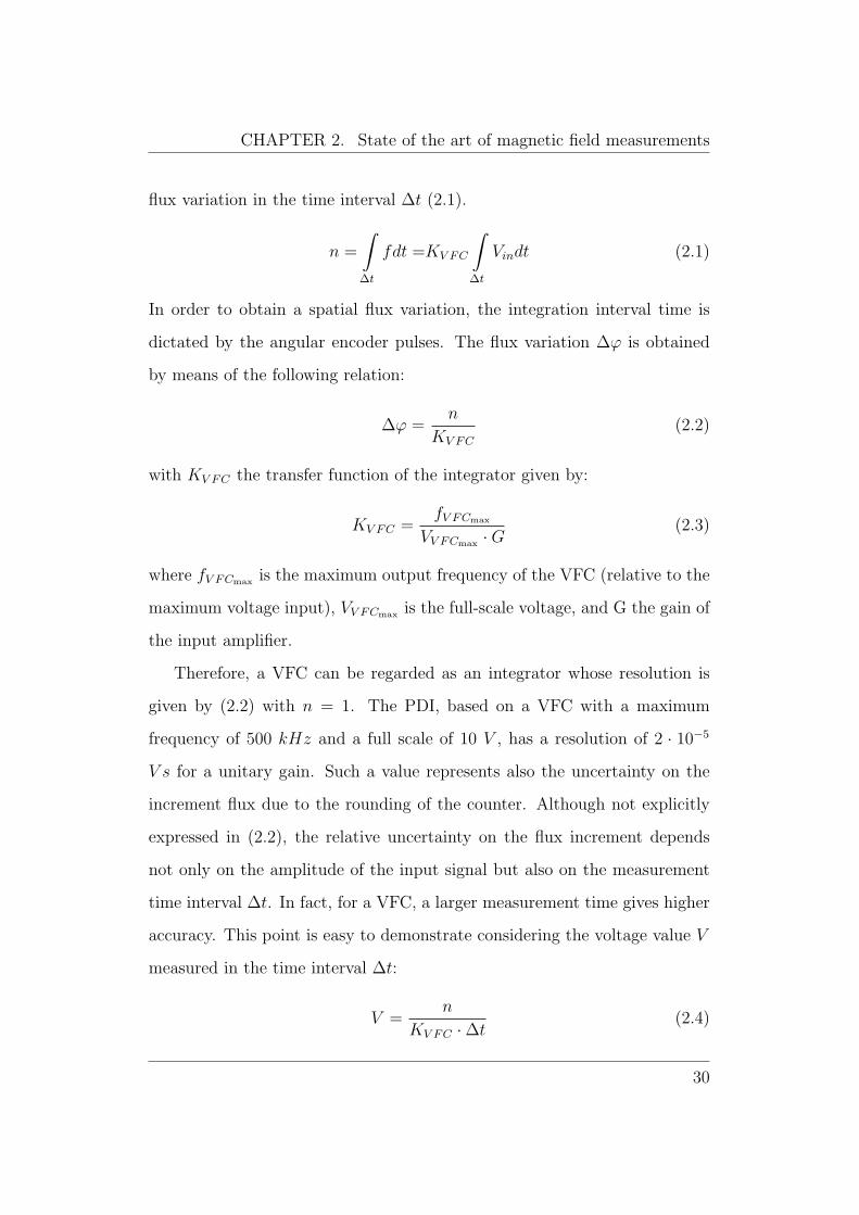
CHAPTER 2. State of the art of magnetic field measurements
flux variation in the time interval ∆t (2.1).
n =
∫∆t
fdt =KV FC
∫∆t
Vindt (2.1)
In order to obtain a spatial flux variation, the integration interval time is
dictated by the angular encoder pulses. The flux variation ∆ϕ is obtained
by means of the following relation:
∆ϕ =n
KV FC
(2.2)
with KV FC the transfer function of the integrator given by:
KV FC =fV FCmax
VV FCmax ·G(2.3)
where fV FCmax is the maximum output frequency of the VFC (relative to the
maximum voltage input), VV FCmax is the full-scale voltage, and G the gain of
the input amplifier.
Therefore, a VFC can be regarded as an integrator whose resolution is
given by (2.2) with n = 1. The PDI, based on a VFC with a maximum
frequency of 500 kHz and a full scale of 10 V , has a resolution of 2 · 10−5
V s for a unitary gain. Such a value represents also the uncertainty on the
increment flux due to the rounding of the counter. Although not explicitly
expressed in (2.2), the relative uncertainty on the flux increment depends
not only on the amplitude of the input signal but also on the measurement
time interval ∆t. In fact, for a VFC, a larger measurement time gives higher
accuracy. This point is easy to demonstrate considering the voltage value V
measured in the time interval ∆t:
V =n
KV FC ·∆t(2.4)
30
CHAPTER 2. State of the art of magnetic field measurements
The equivalent of the Least Significant Bit (LSB) for a VFC is obtained by
considering n = 1:
LSBV FC =1
KV FC ·∆t(2.5)
By the definition of the LSB for an AD converter, the number of bit N can
be expressed as:
N = log2(VV FCmax
LSB) = log2(∆t · fV FCmax) = log2(
fV FCmax
fs
) (2.6)
where fs is the inverse of the measurement time ∆t, i.e. the sampling rate.
Therefore, the accuracy of a VFC gets worse at increasing the sampling rate.
In practice, Metrolab specifies a time interval of 1 ms as minimum integration
period [19], which can be used in estimates of the number of bits N .
2.2.2 Technologies from other research centers
A voltage integrator based on the chain of a Programmable Gain Amplifier
(PGA), an ADC, and a Digital Signal Processor (DSP) has been developed
for the measurement of the magnetic field by the rotating coil system at the
Fermi National Accelerator Laboratory (FNAL) [24]. The acquisition card
is the Pentek 6102 [64] and the DSP card is the Pentek 4288 [65]. The
Pentek 6102 is based on a 16-bit ADC with a maximum sampling rate of
250 kS/s. The Pentek 4288 has a DSP at 40 MHz. The communication is
performed through a proprietary high-speed mezzanine bus, Intel Modular
Interface eXtension (MIX). The coil signal is sampled at 40-50 kS/s and then
integrated. The flux values are transferred to the VME accessible memory
and read by the VME control computer. The new instrument results only
5 times faster than the PDI. Further performance details such as resolution
and accuracy are not clearly published.
31
CHAPTER 2. State of the art of magnetic field measurements
In 1999, a new integrator was conceived at Commisariat a l’Energie Atom-
ique (CEA Saclay). The voltage signal is sampled by a 16-bit ADC at a
maximum sampling rate of 100 kS/s and then the data are processed by a
DSP board. An additional time measurement is provided with a resolution
of 5 ns [23]. However, to date the instrument is not available.
A new integrator with high voltage input has been developed also at
the Japan Atomic Energy Research Institute. The instrument uses VFCs
combined with Up-Down Counters (UDC). To reduce errors due to VFCs
input saturation, the new digital integrator is composed of three VFC-UDC
units in parallel with different input ranges. A DSP selects the best integrated
output, according to the input level at a sampling frequency of 10 ks/s [66].
2.2.3 Commercial integrators and rationale for a cus-tom solution
On-market instruments dedicated to voltage integration are mainly based on
an analog circuit.
Wenking model EVI 95 is a long-term accurate integrator [67]. An ana-
logue circuit integrates the input signal up to a precisely set voltage level,
detected by a discriminator circuit. At this discrimination level, the inte-
grating capacitor is discharged to zero immediately and charged again. The
number of discharges is counted by a dual six-decade counter, separately for
each polarity. The instrument is capable to integrate over a time period from
less than 1 s up to more than 10000 hours.
The RDM-Apps VI10 F presents a low-pass active filter, with an ad-
justable cut-off frequency and an adjustable time constant that can be set
by means of a potentiometer or digitally [68].
32
CHAPTER 2. State of the art of magnetic field measurements
Both the instruments require a fine adjustment of the offset drift of the
analog circuit and are not fast enough to satisfy the current requirements for
dynamic magnetic measurements.
As far as commercially-available digital instruments are concerned, many
cards, based on different platforms, such as VME bus, PCI/CPCI/PXI bus,
usable as integrators, are proposed on the market. They provide ADCs and
signal processing capabilities on a single card or on two cards communicating
on the same bus platform [25], [26], [27], [28], [29], [30].
However, the rotating coils application as well as the other magnetic mea-
surement methods require particular features, detailed in Chapter 3, such as
a wide set of input range, a fine calibration of gain and offset, high accuracy,
and low harmonic distortion, not easy to match on a single card. More-
over, the development of a custom solution and then the knowledge and the
mastery of the card at the hardware level, permits a profitable management
of the internal and external I/O lines by assuring a high operation flexibil-
ity. Such a feature makes the new instrument suitable for laboratory trials.
On this basis, the development of a new custom integrator was launched at
CERN, as a main scope of this thesis work, under a cooperation with the
Department of Engineering of the University of Sannio.
33

Chapter 3
Instrument requirements andmain issues for fast magneticmeasurements
The integrator requirements are imposed by the new rotating coils, as well as
by the will of designing a general-purpose card, to be used for other magnet
measurements methods too.
In this chapter, after recalling the main quantities of the rotating coils
method, the main challenges of frequency bandwidth, resolution, accuracy,
harmonic distortion, offset, and drift are analyzed.
3.1 Analysis of the rotating coil method
The rotating coil method is based on the Faraday’s law. A set of coil-based
transducers are placed in the magnet bores, supported by a shaft turning
coaxially inside the magnet (see 2.1.1).
The coil signal is a sine wave whose frequency fin depends on the number
of poles of the magnet n (an even number ≥ 2) and on the rotation speed ω
34
CHAPTER 3. Instrument requirements and main issues for fast magneticmeasurements
(3.1).
fin = ω · n2
(3.1)
Therefore, a complete turn represents an integer number of periods of the
input signal.
The amplitude of the coil signal depends on the magnetic field strength
and the transducer sensitivity. For a coil rotating in a magnetic field B, at
speed ω, with an equivalent surface Seq, given by its actual surface multiplied
by the number of turns, the sine wave amplitude V is given by (3.2):
V = 2 · π ·B · Seq · ω (3.2)
The coil signal is integrated in the angular domain, by exploiting the pulses
of an encoder mounted on the shaft, in order to get the magnetic flux ϕ(θ).
The flux sampling rate ft depends on the rotation speed ω and on the number
of points per turn Nt, according to (3.3).
ft = ω ·Nt (3.3)
In turn, Nt depends on the encoder resolution and on the multiplier/divider
factor of the prescaler board used to condition the encoder pulses. The flux
sampling rate ft is also called trigger frequency, because it represents the
frequency of the pulses defining the angular intervals of the integration.
The results ϕ(θ) of the measurement over a single complete turn coil is
analyzed in the frequency domain in order to get the field harmonics (see
8.1.1). The FFT resolution ∆f , equal to the rotation speed ω, is always
proper to analyze the coil signal correctly, whatever be fin (3.1).
Finally, the Nyquist limit over a single turn is given by (3.4).
fNyquist = ω · Nt
2(3.4)
35
CHAPTER 3. Instrument requirements and main issues for fast magneticmeasurements
The above considerations are the analytical basis to analyze the main re-
quirements for the new integrator.
3.2 Frequency bandwidth
The frequency bandwidth is determined by the flux sampling rate ft, de-
pending on ω and Nt (3.3).
A single turn of coil is needed to evaluate the field harmonics in the
angular domain. A faster rotation gives a lower update time of the field har-
monics, thus the new rotating coils, based on the MRU, have been designed
to rotate up to 10 rps, in order to permit a field quality analysis at a rate up
to 10 Hz. The rotation speed is increased by a factor 10 with respect to the
previous TRU system (∼ 0.8 rps).
As far as Nt is concerned, an angular resolution of 256 points per turn
was exploited during the series test of the LHC magnets, because it is enough
to appreciate up to the 15th harmonic by means of an FFT calculation (3.4).
However, a higher resolution allows analyzing the flux more accurately, as
well as exploiting numerical algorithms based on sliding FFT windows [16].
Therefore, a target of 8192 poits per turn is assigned as maximum angular
resolution.
Altogether, for rotating coil applications, by considering the maximum
rotation speed of 10 rps and the maximum angular resolution of 8192 points
per turn, a flux sampling rate of about 150 kS/s was fixed as target. Such a
rate is large enough to cover other magnetic measurement techniques too.
36
CHAPTER 3. Instrument requirements and main issues for fast magneticmeasurements
3.3 Resolution, accuracy, and harmonic dis-
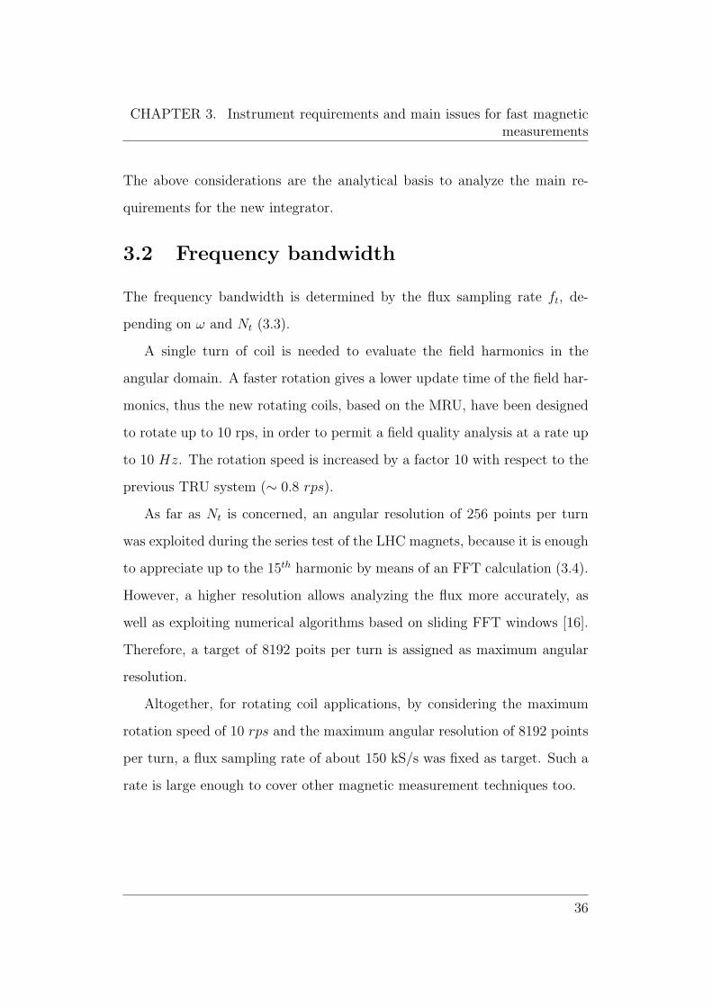
tortion
The VFC of the PDI is intrinsically an integrator, whose resolution depends
on the measurement time (see 2.2.1), determined by the trigger frequency
ft. The new rotating coil system turns faster, thus the trigger frequency
increases, i.e. the integration time between two trigger pulses decreases.
Consequently, the expected amplitude of the flux increment decreases, by
requiring a higher resolution to be appreciated. In Fig. 3.1, the working area
of the new and old rotating coils, based on the MRU and TRU respectively,
are depicted as a function of flux resolution and integration time. The flux
values of the TRU- (2) and MRU- (◦) based systems were evaluated by
considering induction magnetic fields, spanning from 1 to 10 T , at typical
integration time values of the two systems.
The new rotating system requires a higher resolution at a lower integra-
tion time. Therefore, with such requirements the VFC principle turns out to
be not adequate anymore.
Other ADC architectures whit performance independent on the measure-
ment time, may result more suitable for fast magnetic measurements. Their
performance can be assessed by the Signal-to-Noise Ratio (SNR) (3.5) of the
coil signal, a generic figure of merit for comparing AD converters.
SNR = 10 · log(Psig
Pn
) (3.5)
The SNR of the old rotating coils system is evaluated by considering the
results of the tests for the LHC magnets carried out at low- (warm condition)
and high- energy (cold condition) [50], [51], [17].
The power of the coil signal Psig is evaluated by assessing the amplitude
37
CHAPTER 3. Instrument requirements and main issues for fast magneticmeasurements
Figure 3.1: Comparison between TRU- (2) and MRU- (◦) based systems: flux resolutionas a function of the integration time.
of the sinusoidal input signal, related to the magnetic field strength and to
the transducer sensitivity (3.2).
The noise power of input signal Pn is evaluated by using the results of
the series test, under the assumption that the uncertainty of the main field
and its harmonics is due to an additive gaussian white noise N(0, σV ). Thus,
it is possible to relate the uncertainty of the ith field harmonic σi to σV by
means of the following formula:
σ2i =
σ2V
fs/2· 1
(2 · π)2 ·∆f
(i · fin)2 − ∆f2
4
(3.6)
where fs is the sampling rate, ∆f is the FFT resolution, i is the order of
the harmonic, and fin is the frequency of the input signal1. By inverting
the (3.6), σV was evaluated. The typical SNR values of the old generation
of rotating coils (2) are depicted in Fig. 3.2 as a function of the trigger
frequency.
Under the assumption that the old and the new rotating coil system
1Such a result comes up from a frequency domain analysis whose details are reportedlater in 5.1
38
CHAPTER 3. Instrument requirements and main issues for fast magneticmeasurements
are characterized by the same Pn, the working areas of the new one can be
obtained by studying Psig at increasing the rotation speed.
The sensitivity factor k = ω · Seq of the rotating coil is considered. The
Seq of the new rotating coils results 4 times lower than the old ones because
the number of turns was reduced of a factor 4. Conversely, the new MRU-
based system can rotate at a higher speed than the previous one (TRU).
Considering the sensitivity ratio ∆ as:
∆ =ωMRU · SeqMRU
ωTRU · SeqTRU
=1
4
ωMRU
ωTRU
(3.7)
an increase of a factor 4 of the rotation speed will give the same sensitivity
coefficient k for both the systems.
In Fig. 3.2, the prediction of the SNR values of the new rotating coil
are depicted for two values of ∆. For ∆ = 1 (◦), a rotation speed 4 times
greater than the typical TRU speed (0.8 rps) was considered. For ∆ ' 3 (�),
the maximum MRU rotation speed of 10 rps was considered and the SNR
values increase of about 9 dB. Obviously, at increasing the rotation speed,
the trigger frequency gets higher too.
Apart SNR, the instrument must exhibit also low non-linearity because
main magnetic properties to be measured are the field harmonics. Therefore,
a performance target of ±10 ppm relative to the instrument full scale, is
assigned for the static integral non-linearity.
3.4 Gain and offset stability
As above said, the range of the input signal depends on the magnetic field
strength as well as on the transducer properties. As an example, the coil
sensitivity varies according to many factors, such as the number of turns, the
39
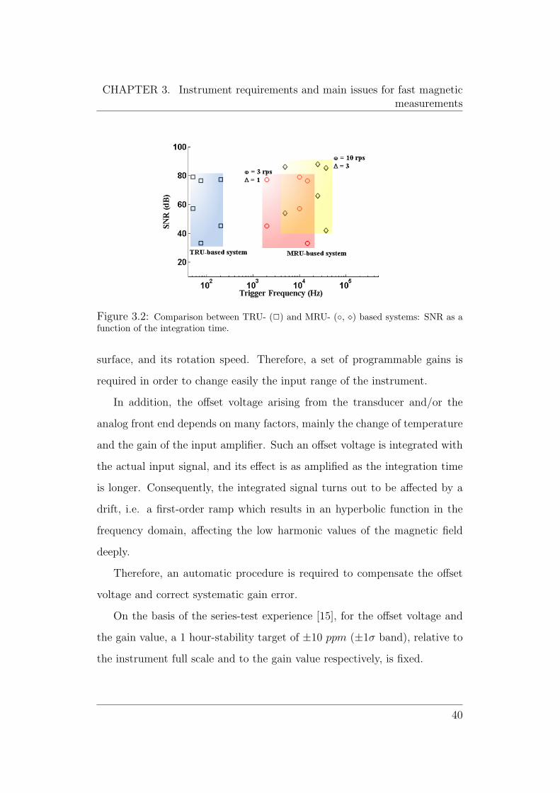
CHAPTER 3. Instrument requirements and main issues for fast magneticmeasurements
Figure 3.2: Comparison between TRU- (2) and MRU- (◦, �) based systems: SNR as afunction of the integration time.
surface, and its rotation speed. Therefore, a set of programmable gains is
required in order to change easily the input range of the instrument.
In addition, the offset voltage arising from the transducer and/or the
analog front end depends on many factors, mainly the change of temperature
and the gain of the input amplifier. Such an offset voltage is integrated with
the actual input signal, and its effect is as amplified as the integration time
is longer. Consequently, the integrated signal turns out to be affected by a
drift, i.e. a first-order ramp which results in an hyperbolic function in the
frequency domain, affecting the low harmonic values of the magnetic field
deeply.
Therefore, an automatic procedure is required to compensate the offset
voltage and correct systematic gain error.
On the basis of the series-test experience [15], for the offset voltage and
the gain value, a 1 hour-stability target of ±10 ppm (±1σ band), relative to
the instrument full scale and to the gain value respectively, is fixed.
40
Chapter 4
Conceptual design
The analysis of the new requirements for magnetic measurements and the
overview of the state-of-art integrator performance highlighted the need of
designing a new instrument, the Fast Digital Integrator (FDI). In this Chap-
ter, the proposal, the working principle, the architecture, and the measure-
ment algorithm of the instrument are described.
4.1 Proposal
In the initial phase of the conceptual design of the instrument, various op-
tions were considered, including Successive Approximation Register (SAR)
and Delta-Sigma (∆−Σ) ADCs [69]. In Fig. 4.1, the expected performance
of the various options are reported in terms of SNR as a function of the
flux sampling rate (trigger frequency), compared to the ideal performance of
the PDI (see 2.2.1) and to the working areas of both old and new rotating
coils. The PDI is based on a VFC, i.e. a first-order ∆-Σ modulator. As well
known, in ∆-Σ converters, the SNR increases according to the oversampling
ratio (i.e., the ratio between sampling and trigger rates) proportionally. In
principle, the performance of ∆-Σ converters can be boosted by increasing
41
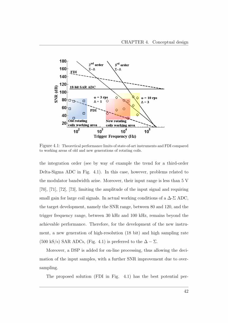
CHAPTER 4. Conceptual design
Figure 4.1: Theoretical performance limits of state-of-art instruments and FDI comparedto working areas of old and new generations of rotating coils.
the integration order (see by way of example the trend for a third-order
Delta-Sigma ADC in Fig. 4.1). In this case, however, problems related to
the modulator bandwidth arise. Moreover, their input range is less than 5 V
[70], [71], [72], [73], limiting the amplitude of the input signal and requiring
small gain for large coil signals. In actual working conditions of a ∆-Σ ADC,
the target development, namely the SNR range, between 80 and 120, and the
trigger frequency range, between 30 kHz and 100 kHz, remains beyond the
achievable performance. Therefore, for the development of the new instru-
ment, a new generation of high-resolution (18 bit) and high sampling rate
(500 kS/s) SAR ADCs, (Fig. 4.1) is preferred to the ∆− Σ.
Moreover, a DSP is added for on-line processing, thus allowing the deci-
mation of the input samples, with a further SNR improvement due to over-
sampling.
The proposed solution (FDI in Fig. 4.1) has the best potential per-
42
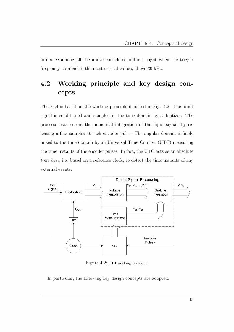
CHAPTER 4. Conceptual design
formance among all the above considered options, right when the trigger
frequency approaches the most critical values, above 30 kHz.
4.2 Working principle and key design con-
cepts
The FDI is based on the working principle depicted in Fig. 4.2. The input
signal is conditioned and sampled in the time domain by a digitizer. The
processor carries out the numerical integration of the input signal, by re-
leasing a flux samples at each encoder pulse. The angular domain is finely
linked to the time domain by an Universal Time Counter (UTC) measuring
the time instants of the encoder pulses. In fact, the UTC acts as an absolute
time base, i.e. based on a reference clock, to detect the time instants of any
external events.
Figure 4.2: FDI working principle.
In particular, the following key design concepts are adopted:
43
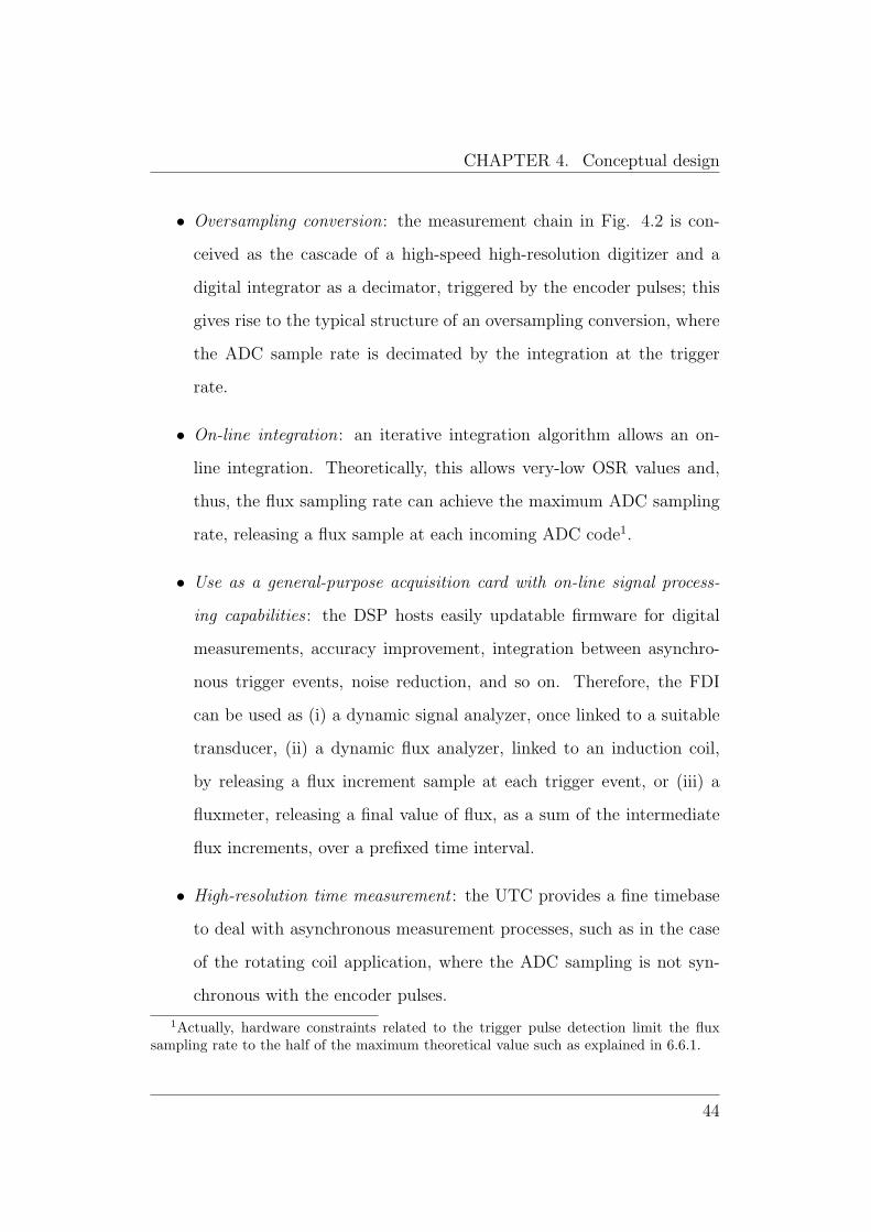
CHAPTER 4. Conceptual design
• Oversampling conversion: the measurement chain in Fig. 4.2 is con-
ceived as the cascade of a high-speed high-resolution digitizer and a
digital integrator as a decimator, triggered by the encoder pulses; this
gives rise to the typical structure of an oversampling conversion, where
the ADC sample rate is decimated by the integration at the trigger
rate.
• On-line integration: an iterative integration algorithm allows an on-
line integration. Theoretically, this allows very-low OSR values and,
thus, the flux sampling rate can achieve the maximum ADC sampling
rate, releasing a flux sample at each incoming ADC code1.
• Use as a general-purpose acquisition card with on-line signal process-
ing capabilities : the DSP hosts easily updatable firmware for digital
measurements, accuracy improvement, integration between asynchro-
nous trigger events, noise reduction, and so on. Therefore, the FDI
can be used as (i) a dynamic signal analyzer, once linked to a suitable
transducer, (ii) a dynamic flux analyzer, linked to an induction coil,
by releasing a flux increment sample at each trigger event, or (iii) a
fluxmeter, releasing a final value of flux, as a sum of the intermediate
flux increments, over a prefixed time interval.
• High-resolution time measurement : the UTC provides a fine timebase
to deal with asynchronous measurement processes, such as in the case
of the rotating coil application, where the ADC sampling is not syn-
chronous with the encoder pulses.
1Actually, hardware constraints related to the trigger pulse detection limit the fluxsampling rate to the half of the maximum theoretical value such as explained in 6.6.1.
44
CHAPTER 4. Conceptual design
• Differential measurement analog chain: programmable gain amplifica-
tion and analog-to-digital conversion are fully differential in order to
increase the Common Mode Rejection Ratio (CMRR), for satisfying
accuracy requirements at higher trigger frequency and lowest levels of
input signal (see 6).
• Self-calibration: the calibration of the analog front-end is carried out
automatically through the following steps: (i) offset calibration with
an input short circuit, (ii) gain calibration, and (iii) offset calibration
with the coil signal at the input (see 6).
4.3 The architecture
The above principle and concepts are synthesized in the FDI conceptual ar-
chitecture of Fig. 4.3. The input signal arising from the coil is conditioned by
a differential Programmable Gain Amplifier (PGA) provided by the above-
mentioned automatic calibration and correction of gain and offset errors. The
conditioned signal is digitized by the SAR ADC. A DSP supervises the board
and processes the data. A Field-Programmable Gate Array (FPGA) acts as
I/O processor: it supervises the PGA operations at low level, implements the
calibration and the correction of offset and gain, and provides the interface
for the board bus. The PXI bus is exploited for the remote control of the
instrument.
45
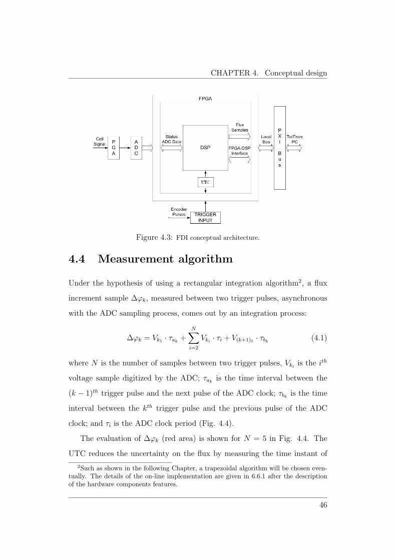
CHAPTER 4. Conceptual design
Figure 4.3: FDI conceptual architecture.
4.4 Measurement algorithm
Under the hypothesis of using a rectangular integration algorithm2, a flux
increment sample ∆ϕk, measured between two trigger pulses, asynchronous
with the ADC sampling process, comes out by an integration process:
∆ϕk = Vk1 · τak+
N∑i=2
Vki· τi + V(k+1)1 · τbk
(4.1)
where N is the number of samples between two trigger pulses, Vkiis the ith
voltage sample digitized by the ADC; τakis the time interval between the
(k − 1)th trigger pulse and the next pulse of the ADC clock; τbkis the time
interval between the kth trigger pulse and the previous pulse of the ADC
clock; and τi is the ADC clock period (Fig. 4.4).
The evaluation of ∆ϕk (red area) is shown for N = 5 in Fig. 4.4. The
UTC reduces the uncertainty on the flux by measuring the time instant of
2Such as shown in the following Chapter, a trapezoidal algorithm will be chosen even-tually. The details of the on-line implementation are given in 6.6.1 after the descriptionof the hardware components features.
46
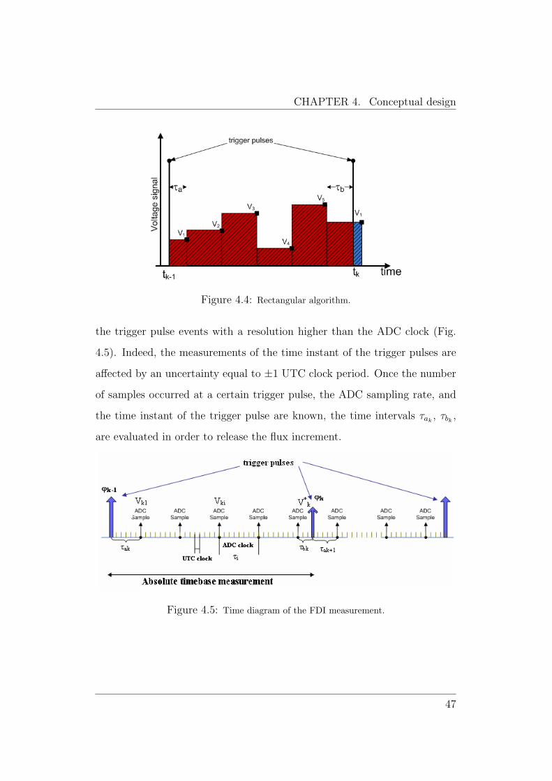
CHAPTER 4. Conceptual design
Figure 4.4: Rectangular algorithm.
the trigger pulse events with a resolution higher than the ADC clock (Fig.
4.5). Indeed, the measurements of the time instant of the trigger pulses are
affected by an uncertainty equal to ±1 UTC clock period. Once the number
of samples occurred at a certain trigger pulse, the ADC sampling rate, and
the time instant of the trigger pulse are known, the time intervals τak, τbk
,
are evaluated in order to release the flux increment.
Figure 4.5: Time diagram of the FDI measurement.
47
Chapter 5
Metrological analysis
Theoretically, the conceptual architecture allows the FDI to face the new
challenges for magnetic measurements. However, the UTC, the PGA, and
the AD converter must exhibit an adequate accuracy level in order to satisfy
the requirements.
In this Chapter, the FDI key concepts are verified by studying the effects
on the performance of the uncertainty sources, the deterministic errors, and
the main instrument parameters.
First an analytical study is carried out in order to understand the impact
of single factors on the instrument uncertainty.
Then, a behavioral model of the FDI is implemented and the effects
of each factors on the performance are studied separately by means of a
preliminary numerical analysis [31].
Finally, on the basis of these preliminary results and of the first experi-
mental tests on a FDI prototype, a systematic assessment of the performance
over the parameter space as a whole is carried out, by means of a compre-
hensive numerical analysis based on statistical techniques [32].
48
CHAPTER 5. Metrological analysis
5.1 Analytical study
The analytical study is carried out by referring to the evaluation of the flux
increment ∆ϕ between two trigger pulses under the assumption of using a
rectangular algorithm (see 4.4). The formula is reported (5.1).
∆ϕk = Vk1 · τak+
N∑i=2
Vki· τi + V(k+1)1 · τbk
(5.1)
The uncertainty sources affects the samples Vk (amplitude domain), the sam-
pling period τi (time domain), and the measurement of the trigger instants,
i.e. τakand τbk
(time domain).
In the following Sections, the uncertainty sources, arising from the time
measurement, i.e. time domain and the input signal acquisition, i.e. ampli-
tude domain are analyzed.
5.1.1 Time-domain uncertainty
The ADC sampling rate is derived by the UTC clock by means of a divider.
The uncertainty of the time interval τi, depending on the uncertainty of the
divider and the aperture time of the ADC, will not be investigated. In fact,
considering the hardware component, it can be considered as negligible in
comparison to the other uncertainty sources (see 5.2.3).
The uncertainty sources in the time domain affects the evaluation of the
flux increment ∆ϕ, such as shown in (5.2),
σ∆ϕk(τa)=∂∆ϕk
∂τaστa = Vk1 · στa
σ∆ϕk(τb)=∂∆ϕk
∂τbστb
= V(k+1)1 · στb(5.2)
49
CHAPTER 5. Metrological analysis
where σ∆ϕk(τa)and σ∆ϕk(τb)
are the flux increment uncertainty due to στa
and στb(the uncertainty of τa and τb), respectively. Assumed that στa and
στbare determined by the rounding of the UTC (a digital counter), such an
uncertainty source can be modeled as a uniform random variable Uτ , whose
support is equal to twice the UTC clock period (5.3).
στa =τclock√
3(5.3)
Moreover, an actual UTC is also affected by a jitter, considered as a gaussian
random variable ∼ Nτ (0, στjit), that influences the flux uncertainty analo-
gously to the UTC rounding (5.4).
σ∆ϕkb(τ) =∂∆ϕk
∂τbστjit
= V(k+1)1 · στjit(5.4)
As a matter of fact, the effects of the time uncertainty on the flux is given
by the UTC uncertainty, weighted by the amplitude of the voltage signal (5.2,
5.4). The time uncertainty is not cumulated because the UTC value is always
referred to the start of the measurement (absolute measurement).
5.1.2 Amplitude-domain uncertainty
The effects of the amplitude domain uncertainty on the flux σ∆ϕk(V ) are given
by,
σ∆ϕk(V )∼=∂∆ϕk
∂Vi
σVi·√N ≤ τi · σVi
·√N (5.5)
where N is the number of ADC samples between two trigger pulses (see 4.4),
and σViis the uncertainty of the input signal. Such an uncertainty source is
due to the input stage of the instrument, namely to the PGA and the ADC,
50
CHAPTER 5. Metrological analysis
and will be considered as a gaussian random variable ∼ N(0, σV ), according
to the central limit theorem.
The offset of the input signal was not considered because the FDI is
provided by an automatic algorithm for correcting systematic errors, namely
offset and gain error.
It is worth to note that (5.5) is an upper bound of σ∆ϕk(V ) because the
uncertainty of two ADC samples in (5.1) is weighted by τa and τb, which are,
of course, less than the ADC sampling period τi.
In (5.5), σViis weighted by the ADC sampling period and by the square
root of the number of voltage samples between two trigger pulses. Therefore,
the effects of the amplitude domain uncertainty on the flux increase according
to the measurement time.
Further considerations can be carried out by analyzing the effect of voltage
signal noise in the Fourier domain. In addition to the integration operation,
the flux signal is also the result of an oversampling process. In fact, the
voltage signal is sampled in the time domain at the ADC sampling rate, while
the flux increments are released at each trigger pulse. The ratio between the
ADC sampling rate and the flux sampling rate is the oversampling factor k.
Whatever the amplitude domain sources be, σ2V is the noise power over the
bandwidth fs/2, determined by the ADC sampling rate fs. The noise power
σ2int after the integration and the downsampling processes, can be evaluated
by integrating the power spectrum density of the noise PSDnoiseV(5.6, 5.7),
PSDnoiseV=
σ2V
fs/2(5.6)
σ2int =
∫ fs2k
0+
σ2V
fs/2· 1
(2 · π · f)2df (5.7)
where fs/(2k) is the bandwidth imposed by the downsampling process (k is
51
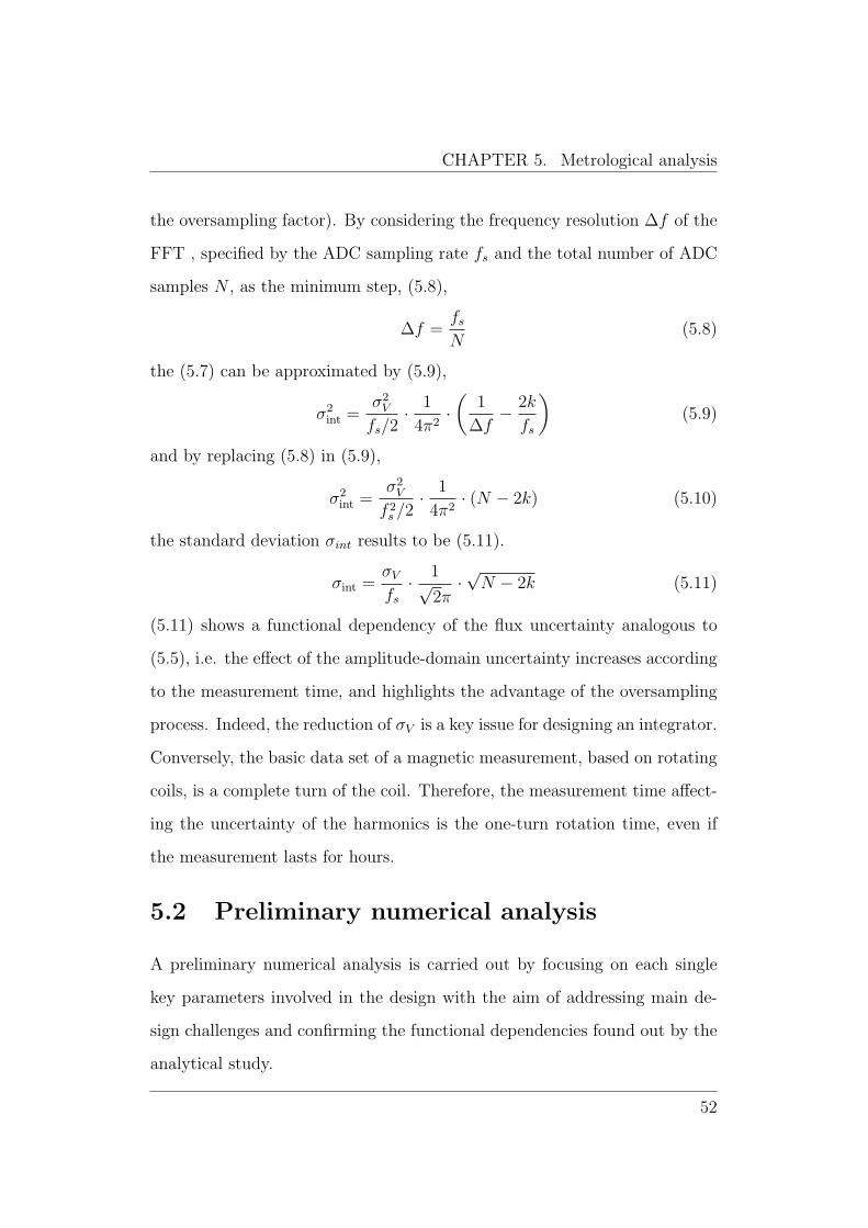
CHAPTER 5. Metrological analysis
the oversampling factor). By considering the frequency resolution ∆f of the
FFT , specified by the ADC sampling rate fs and the total number of ADC
samples N , as the minimum step, (5.8),
∆f =fs
N(5.8)
the (5.7) can be approximated by (5.9),
σ2int =
σ2V
fs/2· 1
4π2·(
1
∆f− 2k
fs
)(5.9)
and by replacing (5.8) in (5.9),
σ2int =
σ2V
f 2s /2
· 1
4π2· (N − 2k) (5.10)
the standard deviation σint results to be (5.11).
σint =σV
fs
· 1√2π
·√N − 2k (5.11)
(5.11) shows a functional dependency of the flux uncertainty analogous to
(5.5), i.e. the effect of the amplitude-domain uncertainty increases according
to the measurement time, and highlights the advantage of the oversampling
process. Indeed, the reduction of σV is a key issue for designing an integrator.
Conversely, the basic data set of a magnetic measurement, based on rotating
coils, is a complete turn of the coil. Therefore, the measurement time affect-
ing the uncertainty of the harmonics is the one-turn rotation time, even if
the measurement lasts for hours.
5.2 Preliminary numerical analysis
A preliminary numerical analysis is carried out by focusing on each single
key parameters involved in the design with the aim of addressing main de-
sign challenges and confirming the functional dependencies found out by the
analytical study.
52
CHAPTER 5. Metrological analysis
The parameters are (i) the type of integration algorithm, (ii) the ADC
sampling rate, (iii) the use of the UTC, (iv) the UTC uncertainty, and (v)
the acquisition chain noise. The first three parameters are mainly related to
the design, while the uncertainty parameters are investigated to confirm the
analytical study.
Considering a sine wave as input signal, the difference between its ana-
lytical integral and the numerical integral, such as provided by the FDI sim-
ulator, is considered as the figure of merit for evaluating the effects of each
parameter. In the design phase, the numerical error of the FDI integration
is analyzed in order to check the benefit of an ideal high-rate high-resolution
ADC, affected by external uncertainty sources, arising from the time mea-
surement and the analog chain of the instrument. The results are obtained
as statistical average and standard deviation of the error for an experiment
set. The standard deviation of the numerical error is used to analyze the flux
uncertainty because the analytical integral of the input signal is not affected
by uncertainty.
The FDI simulator aims at reproducing the instrument procedure. The
acquisition chain noise is modeled as a gaussian variable ∼ NV (0, σV ). The
18-bit ADC is modeled by means of a transfer function characterized by
218 steps. The DNL error of the digitizer transfer function is simulated by
adding a uniform random noise (±0.5 LSB) to the ideal step size. The
actual UTC is simulated by a numerical counter, whose results are affected
by a gaussian noise ∼ Nτ (0, στ ) and a uniform noise Uτ with support equal
to twice the UTC clock, taking into account the UTC jitter and the finite
UTC resolution, respectively. The DSP functions are implemented by means
of numerical routines. The simulator is implemented in MATLABTM .
53
CHAPTER 5. Metrological analysis
In the following, the results are presented by focusing on (i) the integra-
tion algorithm and the ADC rate, (ii) the use of the UTC, (iii) the time-
domain uncertainty effects, and (iv) the amplitude-domain uncertainty ef-
fects.
5.2.1 Integration algorithm and ADC rate
The error due to the numerical integration is studied at varying the time
step integration, i.e. the ADC sampling rate, and the type of algorithm. The
error, evaluated as the difference between the numerical and the analytical
integral of a sine wave, is a function of the time, thus its Root Mean Square
(RMS) value is considered. For each ADC sampling rate, the integration is
carried out at different flux sampling rate, ranging from 256 to 2048 S/s.
The simulation is done without adding any random noise in order to verify
Figure 5.1: Influence on FDI performance of algorithm type, ADC sampling rate, andflux sampling rate.
the numerical error only.
54
CHAPTER 5. Metrological analysis
Obviously, the trapezoidal algorithm gives better results than the rectan-
gular one (Fig. 5.1). But, the main goal of such an analysis is choosing a
proper value of the ADC sampling period assuring a suitable numerical error
and a computing time low enough to allow the on-line implementation of the
algorithm. The test results show that the trapezoidal rule has an acceptable
computing time so that it can be implemented on line, by assuring a nu-
merical error less than 0.01 µVs (Fig. 5.1) at the maximum ADC sampling
rate (500 kS/s)(see 6.6.1). Thus, the analysis of a numerical algorithm more
performing than the trapezoidal one is useless for the application.
5.2.2 UTC
Without the UTC, the trigger event detection is based on the ADC sampling
period. The influence on FDI performance of the use of an UTC at 50 ns
(the reference clock of the board, see 6) is shown in Fig. 5.2. In case of
a rectangular algorithm (Fig. 5.2a), the RMS error is not affected by the
presence of the UTC significantly. In the case of the trapezoidal algorithm
(Fig. 5.2b), the advantage of the time base presence is evident: performance
is improved by about three orders of magnitude.
5.2.3 Time-domain uncertainty effects
In the time domain, the main uncertainty sources arise from the ADC sam-
pling jitter and the UTC. The ADC sampling jitter is about few nanoseconds,
thus it can be considered negligible with respect to the UTC resolution. The
UTC gives rise to a rounding error in the detection of the trigger event in
any case (although reduced with respect to an ADC-based detection), owing
to its finite resolution (50 ns). Moreover, an actual UTC is also affected by
55
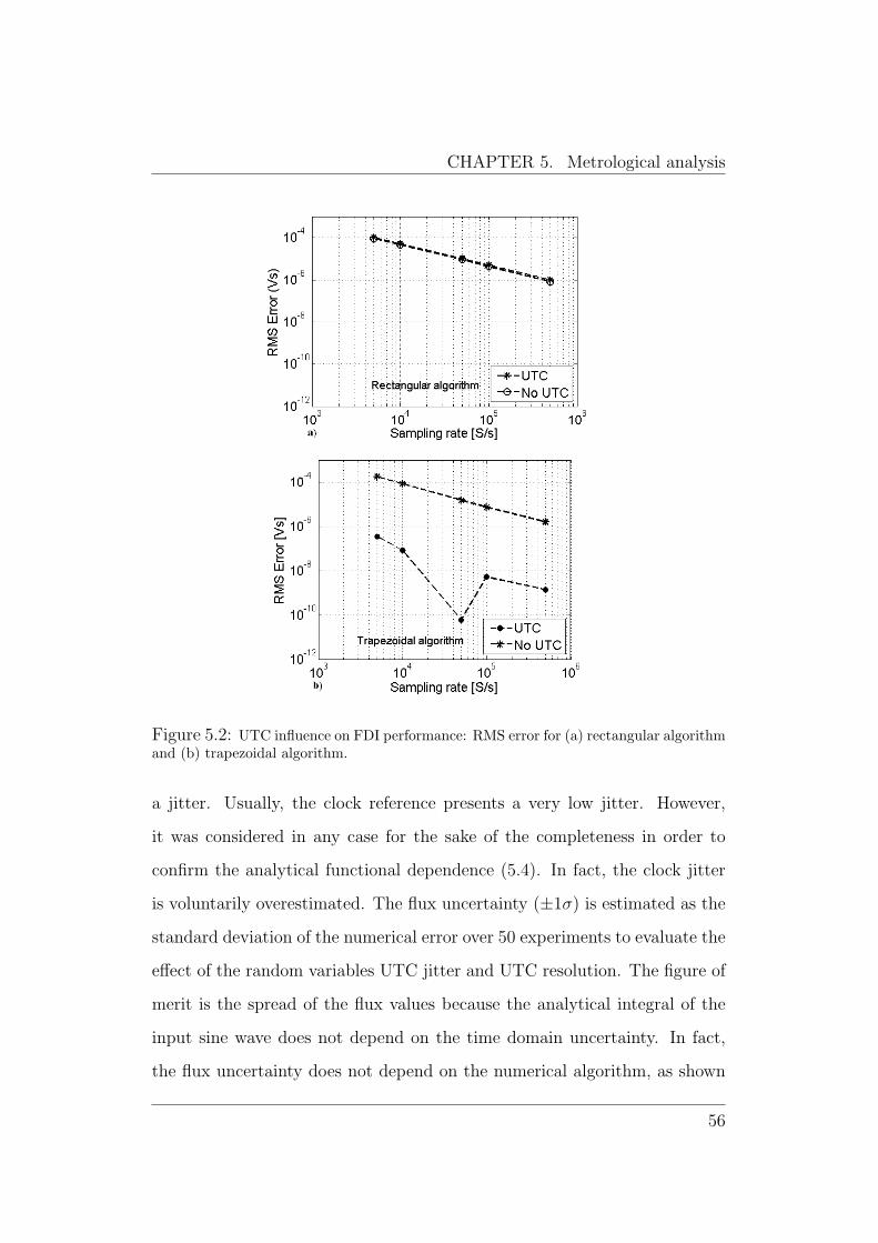
CHAPTER 5. Metrological analysis
Figure 5.2: UTC influence on FDI performance: RMS error for (a) rectangular algorithmand (b) trapezoidal algorithm.
a jitter. Usually, the clock reference presents a very low jitter. However,
it was considered in any case for the sake of the completeness in order to
confirm the analytical functional dependence (5.4). In fact, the clock jitter
is voluntarily overestimated. The flux uncertainty (±1σ) is estimated as the
standard deviation of the numerical error over 50 experiments to evaluate the
effect of the random variables UTC jitter and UTC resolution. The figure of
merit is the spread of the flux values because the analytical integral of the
input sine wave does not depend on the time domain uncertainty. In fact,
the flux uncertainty does not depend on the numerical algorithm, as shown
56
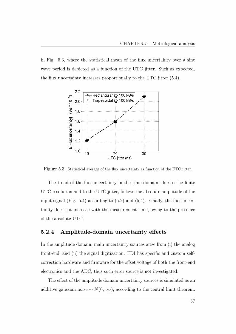
CHAPTER 5. Metrological analysis
in Fig. 5.3, where the statistical mean of the flux uncertainty over a sine
wave period is depicted as a function of the UTC jitter. Such as expected,
the flux uncertainty increases proportionally to the UTC jitter (5.4).
Figure 5.3: Statistical average of the flux uncertainty as function of the UTC jitter.
The trend of the flux uncertainty in the time domain, due to the finite
UTC resolution and to the UTC jitter, follows the absolute amplitude of the
input signal (Fig. 5.4) according to (5.2) and (5.4). Finally, the flux uncer-
tainty does not increase with the measurement time, owing to the presence
of the absolute UTC.
5.2.4 Amplitude-domain uncertainty effects
In the amplitude domain, main uncertainty sources arise from (i) the analog
front-end, and (ii) the signal digitization. FDI has specific and custom self-
correction hardware and firmware for the offset voltage of both the front-end
electronics and the ADC, thus such error source is not investigated.
The effect of the amplitude domain uncertainty sources is simulated as an
additive gaussian noise ∼ N(0, σV ), according to the central limit theorem.
57
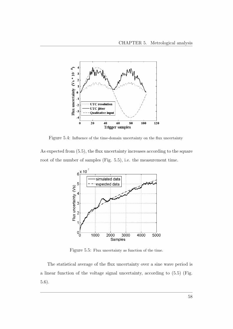
CHAPTER 5. Metrological analysis
Figure 5.4: Influence of the time-domain uncertainty on the flux uncertainty
As expected from (5.5), the flux uncertainty increases according to the square
root of the number of samples (Fig. 5.5), i.e. the measurement time.
Figure 5.5: Flux uncertainty as function of the time.
The statistical average of the flux uncertainty over a sine wave period is
a linear function of the voltage signal uncertainty, according to (5.5) (Fig.
5.6).
58
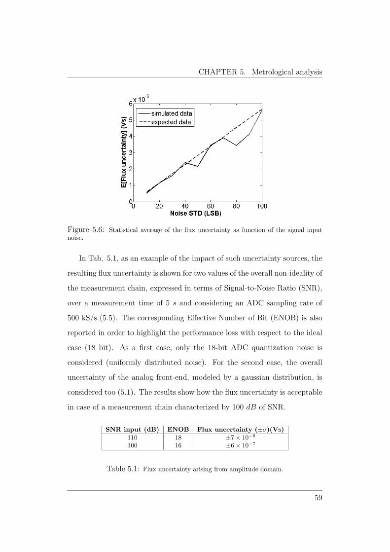
CHAPTER 5. Metrological analysis
Figure 5.6: Statistical average of the flux uncertainty as function of the signal inputnoise.
In Tab. 5.1, as an example of the impact of such uncertainty sources, the
resulting flux uncertainty is shown for two values of the overall non-ideality of
the measurement chain, expressed in terms of Signal-to-Noise Ratio (SNR),
over a measurement time of 5 s and considering an ADC sampling rate of
500 kS/s (5.5). The corresponding Effective Number of Bit (ENOB) is also
reported in order to highlight the performance loss with respect to the ideal
case (18 bit). As a first case, only the 18-bit ADC quantization noise is
considered (uniformly distributed noise). For the second case, the overall
uncertainty of the analog front-end, modeled by a gaussian distribution, is
considered too (5.1). The results show how the flux uncertainty is acceptable
in case of a measurement chain characterized by 100 dB of SNR.
SNR input (dB) ENOB Flux uncertainty (±σ)(Vs)110 18 ±7× 10⁻⁸
100 16 ±6× 10⁻⁷
Table 5.1: Flux uncertainty arising from amplitude domain.
59
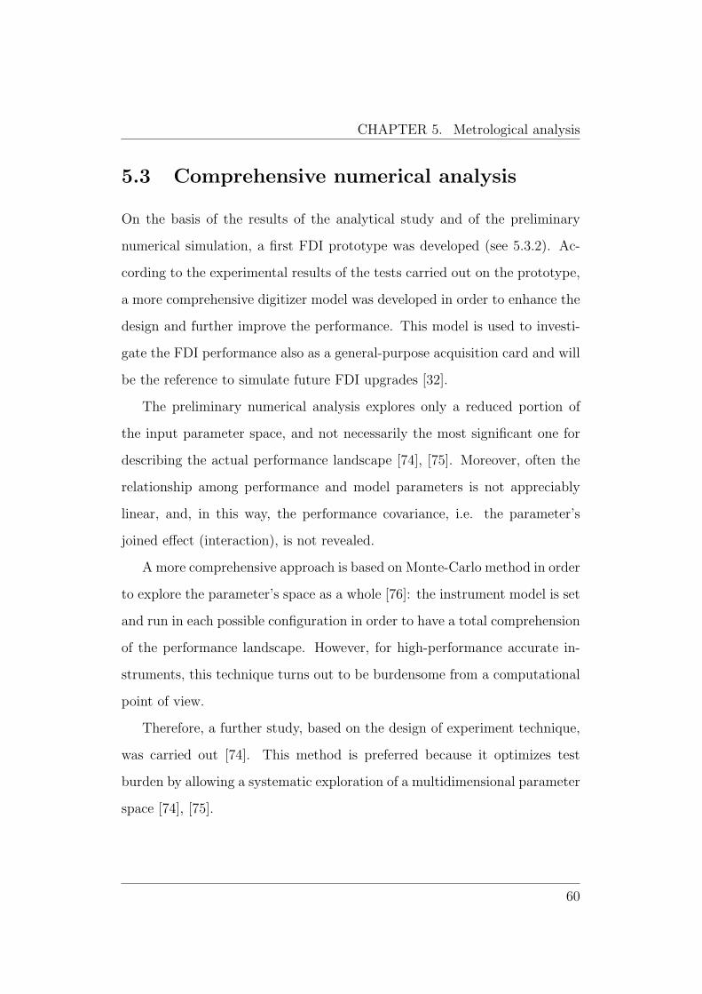
CHAPTER 5. Metrological analysis
5.3 Comprehensive numerical analysis
On the basis of the results of the analytical study and of the preliminary
numerical simulation, a first FDI prototype was developed (see 5.3.2). Ac-
cording to the experimental results of the tests carried out on the prototype,
a more comprehensive digitizer model was developed in order to enhance the
design and further improve the performance. This model is used to investi-
gate the FDI performance also as a general-purpose acquisition card and will
be the reference to simulate future FDI upgrades [32].
The preliminary numerical analysis explores only a reduced portion of
the input parameter space, and not necessarily the most significant one for
describing the actual performance landscape [74], [75]. Moreover, often the
relationship among performance and model parameters is not appreciably
linear, and, in this way, the performance covariance, i.e. the parameter’s
joined effect (interaction), is not revealed.
A more comprehensive approach is based on Monte-Carlo method in order
to explore the parameter’s space as a whole [76]: the instrument model is set
and run in each possible configuration in order to have a total comprehension
of the performance landscape. However, for high-performance accurate in-
struments, this technique turns out to be burdensome from a computational
point of view.
Therefore, a further study, based on the design of experiment technique,
was carried out [74]. This method is preferred because it optimizes test
burden by allowing a systematic exploration of a multidimensional parameter
space [74], [75].
60
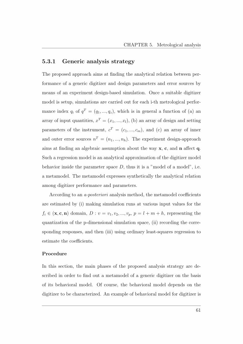
CHAPTER 5. Metrological analysis
5.3.1 Generic analysis strategy
The proposed approach aims at finding the analytical relation between per-
formance of a generic digitizer and design parameters and error sources by
means of an experiment design-based simulation. Once a suitable digitizer
model is setup, simulations are carried out for each i-th metrological perfor-
mance index qi of qT = (q1, ..., qz), which is in general a function of (a) an
array of input quantities, xT = (x1, ..., xl), (b) an array of design and setting
parameters of the instrument, cT = (c1, ..., cm), and (c) an array of inner
and outer error sources nT = (n1, ..., nh). The experiment design-approach
aims at finding an algebraic assumption about the way x, c, and n affect q.
Such a regression model is an analytical approximation of the digitizer model
behavior inside the parameter space D, thus it is a ”model of a model”, i.e.
a metamodel. The metamodel expresses synthetically the analytical relation
among digitizer performance and parameters.
According to an a-posteriori analysis method, the metamodel coefficients
are estimated by (i) making simulation runs at various input values for the
fi ∈ (x, c,n) domain, D : v = v1, v2, ..., vp, p = l + m + h, representing the
quantization of the p-dimensional simulation space, (ii) recording the corre-
sponding responses, and then (iii) using ordinary least-squares regression to
estimate the coefficients.
Procedure
In this section, the main phases of the proposed analysis strategy are de-
scribed in order to find out a metamodel of a generic digitizer on the basis
of its behavioral model. Of course, the behavioral model depends on the
digitizer to be characterized. An example of behavioral model for digitizer is
61
CHAPTER 5. Metrological analysis
given in the Section 5.3.2, where the analysis strategy is applied to the FDI.
The procedure is based on three mains steps (Fig. 5.7): (i) metamodel
definition, (ii) metamodel identification, and (iii) metamodel validation.
Metamodel Definition. As a first step, the metamodel inputs and parame-
ters x, c, and n are defined (parameter definition) (Fig. 5.7), according to the
most critical aspects of the digitizer design. The digitizer performance index
q is selected according to the specific quality aspect of the instrument to be
investigated. They are mainly metrological indexes, static and dynamic, in
the amplitude (e.g. DNL, or INL), time (e.g. stability), and frequency (e.g.
signal-to-noise ratio) domains [34], but also functional performance, such as
efficiency (e.g. throughput rate).
The parameters are identified experimentally by determining in partic-
ular the variation range of each array component (experimental parameter
identification). In this step, an estimation of the central values of the working
ranges for each parameter is obtained, often by means of several identifica-
tion techniques [77]. Once the components of the arrays x, c, and n are
defined, they represent the continuous domain D of the metamodel function
f . According to the particular application, D has to be sampled suitably, in
order to carry out the simulations in a finite number of steps.
The order of the metamodel capable of describing suitably the digitizer
metrological behavior is to be decided. Combinatorial increase of the problem
dimensionality is faced by means of a full-quadratic model [75]. In some cases,
such a choice turns out to be too heavy, thus a first-screening attempt based
on a linear model is carried out.
Metamodel identification. In case of a full-quadratic metamodel, the de-
pendence of the performance on the input array, design and setting parame-
62
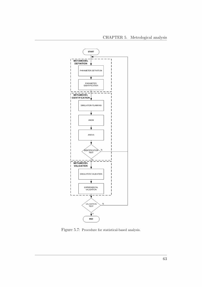
CHAPTER 5. Metrological analysis
Figure 5.7: Procedure for statistical-based analysis.
63
CHAPTER 5. Metrological analysis
ters, and uncertainty sources, is verified by using the ANalysis of COVAriance
(ANCOVA) model:
qi = µi +
p∑k=1
δikvk+
p∑k=1
p∑j=1
dikjvkvj + ε (5.12)
where qi is the i-th performance index, ε represents the uncertainty, µi the
overall mean of the i-th performance, δik the effect on the response of the
k-th parameter, dikj the interaction between the k-th and the j-th parameters
and vk ≡ {0, 1} are dummy variables, equal to 1 or 0 if the corresponding
effect is considered or not, respectively.
Conversely, in order to verify the suitability of a simpler first-order meta-
model, the ANalysis Of VAriance (ANOVA) linear model is usually used:
qi = µi +
p∑k=1
δikvk+ε (5.13)
The metamodel turns out to be a fixed-effects model, if µi and δik are con-
stants and only the error term ε is random [78]. Conversely, if some δik are
random, it is classified as a mixed model. In the following exposition, for
the sake of conciseness, only the first-step analysis based on a first-order
metamodel is considered.
At operating level, the suitability of the metamodel order is verified by:
(i) the simulation planning and running, (ii) the Analysis of Mean (ANOM),
and (iii) the ANOVA. Then, an identification test is carried out in order to
confirm the analysis.
The optimum subset of the simulation domainD is defined by selecting an
experimental plan, according to the number of parameters and their levels,
as well as the desired resolution [75], i.e. the desired information about
covariance between the parameters. Then, the simulations are run according
64
CHAPTER 5. Metrological analysis
to the defined plan.
The main effects of each parameter on the mean response µi are assessed.
In particular, the actual mean of the simulation runs is estimated so that the
main effect of the k-th parameter in any configuration r can be evaluated
as: δikr = mikr − µi , where mikr is the mean of qi in all the runs where the
k-th parameter is in the configuration r (i.e., one of the points of the discrete
domain D).
The significance of the parameter effects is determined by means of ANOVA.
This method is aimed at determining, within a prefixed uncertainty, if a
variation over the mean performance imposed by a corresponding parameter
variation is due to the parameter itself or it can be confused with the model
uncertainty.
In the identification test, the Fisher test can be used to establish the
global parameter F-statistic of the model [78]. If q is an array, the Fisher
test can be also applied to each component separately [79].
If the choice of a first-order metamodel turns out to be correct, the coef-
ficients of a linear regression curve can be theoretically found out. The fitted
linear model could not be of easy identification. In fact, the functional depen-
dency of the performance index on the input parameters are not necessarily
linear. In such cases, the ANOVA model itself can represent the metamodel.
By expressing the effect of the parameter’s variation with respect to the over-
all mean, it forecasts the digitizer performance over the quantized domain D
of the input parameters.
Metamodel validation. The metamodel is validated through Simulation
Validation and Experimental Validation (Fig. 5.7). The Simulation Valida-
tion aims at verifying the goodness of the simulator in itself, as well as of the
65
CHAPTER 5. Metrological analysis
identified metamodel. Performance is evaluated by simulations in points of
the domain D, not considered in the simulation plan. The result is then com-
pared with the metamodel prediction. The Experimental Validation is based
on the same concept: performance of an actual prototype of the instrument
(or of a low-level simulator) in particular working points are measured and
then compared with the metamodel forecasts. To validate the metamodel,
the results must be consistent within the band specified by the uncertainty
of the metamodel.
5.3.2 Application to FDI
The proposed generic approach was applied to the new FDI model, developed
on the basis of the experimental results on a first board prototype. Some
parameters of the preliminary numerical analysis are considered again be-
cause the statistical-based approach aims at investigating comprehensively
and systematically the impact of possible non-ideality sources (n) on the
dynamic distortion and on the SNR (q) of the FDI output, at varying the
working operating conditions, mainly defined by the input (x) and by the
design settings (c ).
In the following, after a description of the FDI prototype board, the FDI
metamodel definition, identification, and validation are illustrated.
FDI prototype
A preliminary prototype of the FDI was realized in order to verify the main
design choices according to the conceptual architecture (see 4.3) and to the
uncertainty analysis (see 5.2). The preliminary characterization of the proto-
type allowed the FDI parameters to be tuned for implementing its statistical
66
CHAPTER 5. Metrological analysis
analysis. Although the prototype did not include the DSP processor yet, it
allowed the main uncertainty sources arising from the analog front-end to be
verified [80].
It is noted that the PGA-ADC chain of the prototype is not optimized
because the launch on the market of the ADC AD7634, selected for the
FDI board was delayed. Therefore, the ADC AD7674 was adopted with
an additional buffer amplifier for adapting the analog signal to its unipolar
differential input [81]. More details about the hardware components are given
in Chapter 6.
FDI metamodel definition
Initially, under the assumption that the parameters n , x, and c are inde-
pendent, a first-order screening metamodel is exploited. In particular, the
resulting non-ideality of the FDI output as a whole has to be analyzed, thus
the metamodel output q is the SIgnal-to-Noise And Distortion ratio (SINAD)
of the computed integral. One of the most important investigation is the as-
sessment of the benefits of the oversampling process on the performance.
Therefore, the input x of the FDI metamodel (Fig. 5.8) is expressed as
Over-Sampling Ratio (OSR), i.e. the ratio between the ADC sampling rate
fs and the trigger frequency ft. On the basis of the preliminary study (see 5.1
and 5.2) main design settings parameters c to be investigated are the type
of integration algorithm (rectangular or trapezoidal), and the possibility of
using the UTC. In the FDI acquisition and processing chain, main significant
non-ideality sources (n) are [82]: the overall acquisition amplitude random
noise (modeled as an additive gaussian noise ∼ NV (0, σV )), the time base
jitter noise (a gaussian noise ∼ Nτ (0, στ )), and the deterministic nonlinearity
67
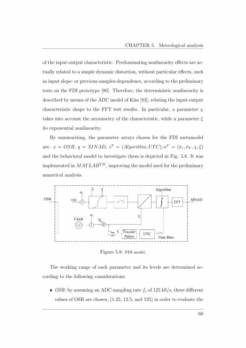
CHAPTER 5. Metrological analysis
of the input-output characteristic. Predominating nonlinearity effects are ac-
tually related to a simple dynamic distortion, without particular effects, such
as input slope- or previous samples-dependence, according to the preliminary
tests on the FDI prototype [80]. Therefore, the deterministic nonlinearity is
described by means of the ADC model of Kim [83], relating the input-output
characteristic shape to the FFT test results. In particular, a parameter χ
takes into account the asymmetry of the characteristic, while a parameter ξ
its exponential nonlinearity.
By summarizing, the parameter arrays chosen for the FDI metamodel
are: x = OSR, q = SINAD, cT = (Algorithm,UTC);nT = (στ , σV , χ, ξ)
and the behavioral model to investigate them is depicted in Fig. 5.8. It was
implemented in MATLABTM , improving the model used for the preliminary
numerical analysis.
Figure 5.8: FDI model.
The working range of each parameter and its levels are determined ac-
cording to the following considerations:
• OSR: by assuming an ADC sampling rate fs of 125 kS/s, three different
values of OSR are chosen, (1.25, 12.5, and 125) in order to evaluate the
68
CHAPTER 5. Metrological analysis
performance for the corresponding values of 100 kHz, 10 kHz, and 1
kHz, in the most interesting range of the trigger frequency ft.
• Time base jitter : it is defined through the reference clock data sheet
[84]. The time uncertainty sources are verified by simulating the jitter
of the main clock used for the UTC and, through a divider, for the
ADC clock.
• Acquisition noise: by assuming a gaussian distribution, the acquisition
noise is derived experimentally [80], according to:
σ2V =
Psig
10(SNR10 )
(5.14)
where SNR is the Signal-to-Noise Ratio in dB (i.e. the SINAD without
the harmonic distortion), Psig is the input signal power, and the noise
power Pnoise over all the bandwidth, is expressed by the variance σ2V .
• ADC non-linearity parameters : according to the above-mentioned Kim’s
two-parameters model [83], a direct relation between the second and
third harmonics amplitude and χ and ξ is derived from the FFT of the
output:
χ = 2AII
A2I
(5.15)
ξ = 4AIII
AI
(5.16)
where Ai represents the amplitude of the i-th harmonic.
In Tab. 5.2, the numerical values of the FDI metamodel parameters,
selected according to the abovementioned criteria and to the test results of
the prototype, are reported. The levels of the UTC jitter and the acquisition
noise are selected deterministically, thus the model (5.13) is a fixed-effects
model.
69
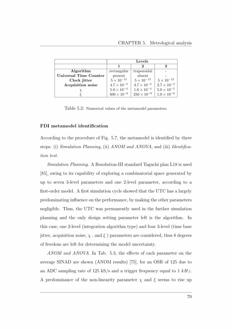
CHAPTER 5. Metrological analysis
Levels1 2 3
Algorithm rectangular trapezoidal -Universal Time Counter present absent -
Clock jitter 5× 10⁻¹⁵ 5× 10⁻¹³ 5× 10⁻¹²
Acquisition noise 4.7× 10⁻⁴ 3.7× 10⁻⁴ 2.7× 10⁻⁴
χ 5.0× 10⁻⁴ 1.6× 10⁻⁴ 5.0× 10⁻⁵
ξ 500× 10−6 250× 10−6 1.0× 10⁻⁶
Table 5.2: Numerical values of the metamodel parameters.
FDI metamodel identification
According to the procedure of Fig. 5.7, the metamodel is identified by three
steps: (i) Simulation Planning, (ii) ANOM and ANOVA, and (iii) Identifica-
tion test.
Simulation Planning. A Resolution-III standard Taguchi plan L18 is used
[85], owing to its capability of exploring a combinatorial space generated by
up to seven 3-level parameters and one 2-level parameter, according to a
first-order model. A first simulation cycle showed that the UTC has a largely
predominating influence on the performance, by making the other parameters
negligible. Thus, the UTC was permanently used in the further simulation
planning and the only design setting parameter left is the algorithm. In
this case, one 2-level (integration algorithm type) and four 3-level (time base
jitter, acquisition noise, χ , and ξ ) parameters are considered, thus 8 degrees
of freedom are left for determining the model uncertainty.
ANOM and ANOVA. In Tab. 5.3, the effects of each parameter on the
average SINAD are shown (ANOM results) [75], for an OSR of 125 due to
an ADC sampling rate of 125 kS/s and a trigger frequency equal to 1 kHz.
A predominance of the non-linearity parameter χ and ξ seems to rise up
70
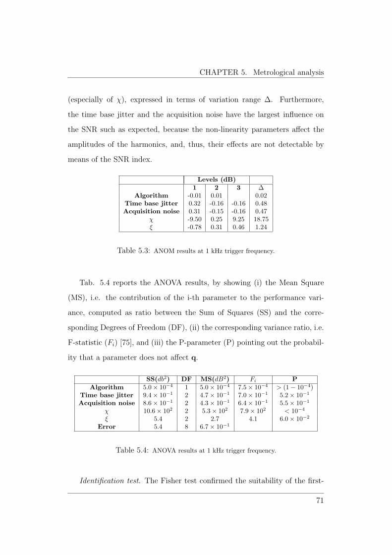
CHAPTER 5. Metrological analysis
(especially of χ), expressed in terms of variation range ∆. Furthermore,
the time base jitter and the acquisition noise have the largest influence on
the SNR such as expected, because the non-linearity parameters affect the
amplitudes of the harmonics, and, thus, their effects are not detectable by
means of the SNR index.
Levels (dB)1 2 3 ∆
Algorithm -0.01 0.01 0.02Time base jitter 0.32 -0.16 -0.16 0.48Acquisition noise 0.31 -0.15 -0.16 0.47
χ -9.50 0.25 9.25 18.75ξ -0.78 0.31 0.46 1.24
Table 5.3: ANOM results at 1 kHz trigger frequency.
Tab. 5.4 reports the ANOVA results, by showing (i) the Mean Square
(MS), i.e. the contribution of the i-th parameter to the performance vari-
ance, computed as ratio between the Sum of Squares (SS) and the corre-
sponding Degrees of Freedom (DF), (ii) the corresponding variance ratio, i.e.
F-statistic (Fi) [75], and (iii) the P-parameter (P) pointing out the probabil-
ity that a parameter does not affect q.
SS(db2) DF MS(dB2) Fi PAlgorithm 5.0× 10⁻⁴ 1 5.0× 10⁻⁴ 7.5× 10⁻⁴ > (1− 10−4)
Time base jitter 9.4× 10⁻¹ 2 4.7× 10⁻¹ 7.0× 10⁻¹ 5.2× 10⁻¹
Acquisition noise 8.6× 10⁻¹ 2 4.3× 10⁻¹ 6.4× 10⁻¹ 5.5× 10⁻¹
χ 10.6× 10² 2 5.3× 10² 7.9× 10² < 10−4
ξ 5.4 2 2.7 4.1 6.0× 10⁻²
Error 5.4 8 6.7× 10⁻¹
Table 5.4: ANOVA results at 1 kHz trigger frequency.
Identification test. The Fisher test confirmed the suitability of the first-
71
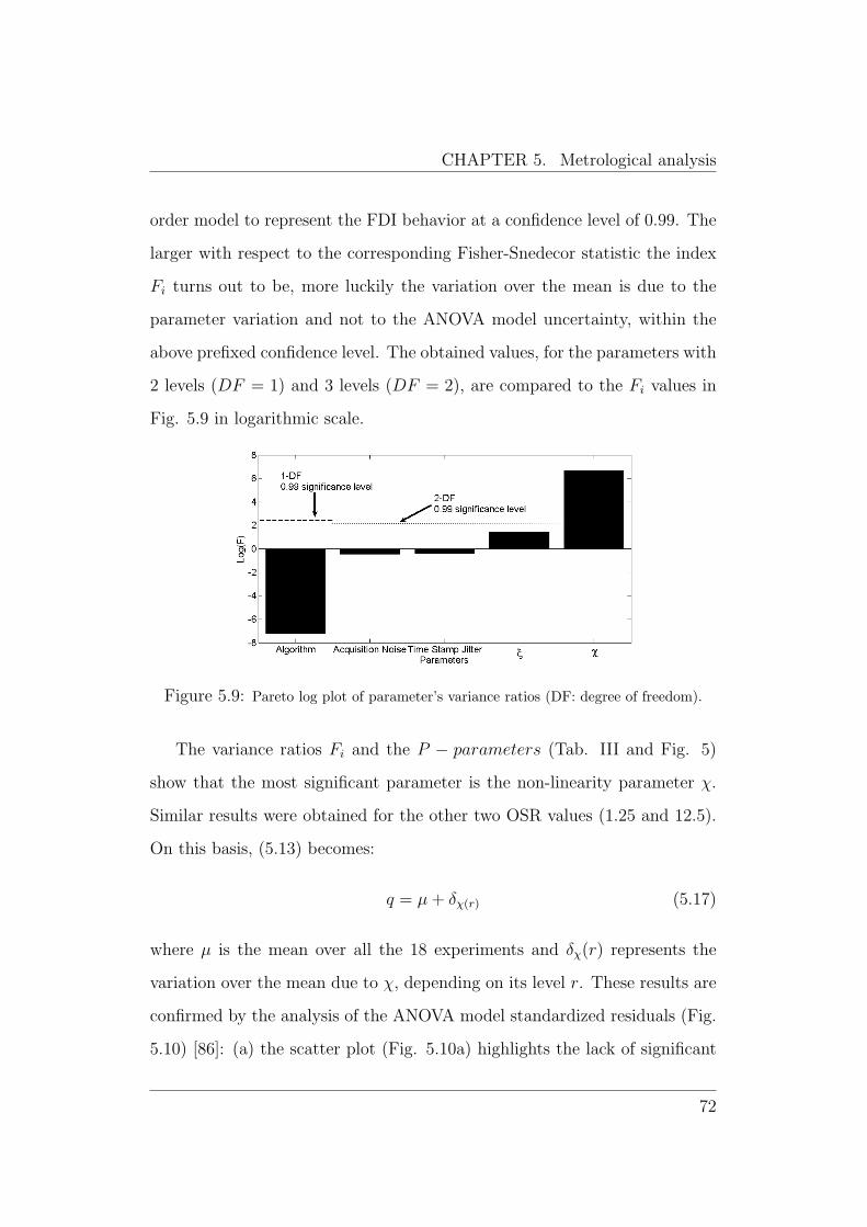
CHAPTER 5. Metrological analysis
order model to represent the FDI behavior at a confidence level of 0.99. The
larger with respect to the corresponding Fisher-Snedecor statistic the index
Fi turns out to be, more luckily the variation over the mean is due to the
parameter variation and not to the ANOVA model uncertainty, within the
above prefixed confidence level. The obtained values, for the parameters with
2 levels (DF = 1) and 3 levels (DF = 2), are compared to the Fi values in
Fig. 5.9 in logarithmic scale.
Figure 5.9: Pareto log plot of parameter’s variance ratios (DF: degree of freedom).
The variance ratios Fi and the P − parameters (Tab. III and Fig. 5)
show that the most significant parameter is the non-linearity parameter χ.
Similar results were obtained for the other two OSR values (1.25 and 12.5).
On this basis, (5.13) becomes:
q = µ+ δχ(r) (5.17)
where µ is the mean over all the 18 experiments and δχ(r) represents the
variation over the mean due to χ, depending on its level r. These results are
confirmed by the analysis of the ANOVA model standardized residuals (Fig.
5.10) [86]: (a) the scatter plot (Fig. 5.10a) highlights the lack of significant
72
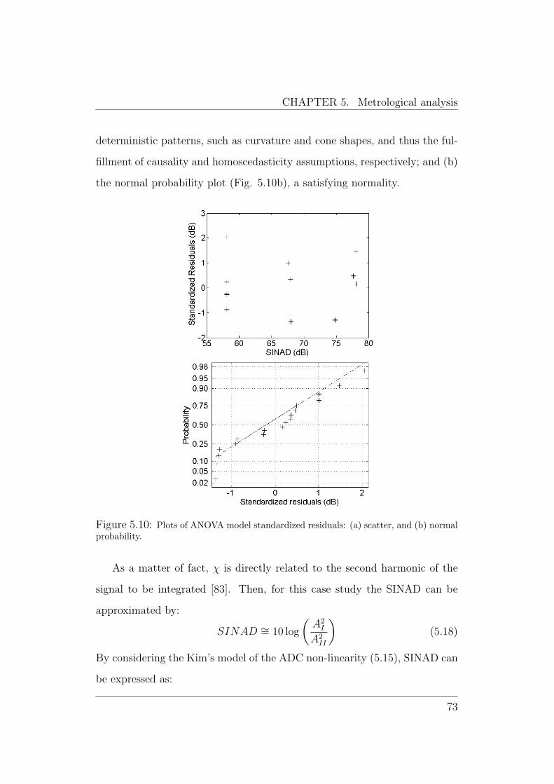
CHAPTER 5. Metrological analysis
deterministic patterns, such as curvature and cone shapes, and thus the ful-
fillment of causality and homoscedasticity assumptions, respectively; and (b)
the normal probability plot (Fig. 5.10b), a satisfying normality.
Figure 5.10: Plots of ANOVA model standardized residuals: (a) scatter, and (b) normalprobability.
As a matter of fact, χ is directly related to the second harmonic of the
signal to be integrated [83]. Then, for this case study the SINAD can be
approximated by:
SINAD ∼= 10 log
(A2
I
A2II
)(5.18)
By considering the Kim’s model of the ADC non-linearity (5.15), SINAD can
be expressed as:
73
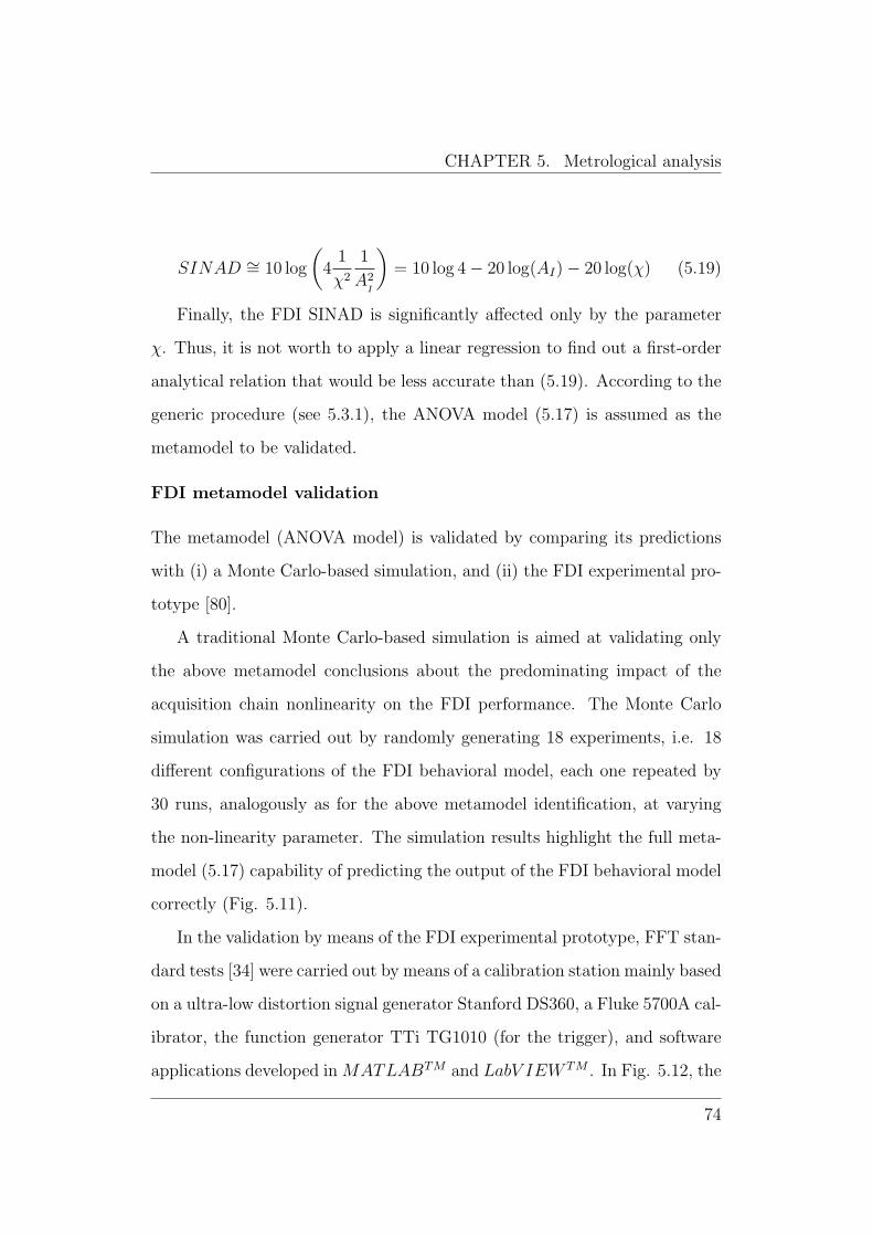
CHAPTER 5. Metrological analysis
SINAD ∼= 10 log
(4
1
χ2
1
A2I
)= 10 log 4− 20 log(AI)− 20 log(χ) (5.19)
Finally, the FDI SINAD is significantly affected only by the parameter
χ. Thus, it is not worth to apply a linear regression to find out a first-order
analytical relation that would be less accurate than (5.19). According to the
generic procedure (see 5.3.1), the ANOVA model (5.17) is assumed as the
metamodel to be validated.
FDI metamodel validation
The metamodel (ANOVA model) is validated by comparing its predictions
with (i) a Monte Carlo-based simulation, and (ii) the FDI experimental pro-
totype [80].
A traditional Monte Carlo-based simulation is aimed at validating only
the above metamodel conclusions about the predominating impact of the
acquisition chain nonlinearity on the FDI performance. The Monte Carlo
simulation was carried out by randomly generating 18 experiments, i.e. 18
different configurations of the FDI behavioral model, each one repeated by
30 runs, analogously as for the above metamodel identification, at varying
the non-linearity parameter. The simulation results highlight the full meta-
model (5.17) capability of predicting the output of the FDI behavioral model
correctly (Fig. 5.11).
In the validation by means of the FDI experimental prototype, FFT stan-
dard tests [34] were carried out by means of a calibration station mainly based
on a ultra-low distortion signal generator Stanford DS360, a Fluke 5700A cal-
ibrator, the function generator TTi TG1010 (for the trigger), and software
applications developed in MATLABTM and LabV IEW TM . In Fig. 5.12, the
74
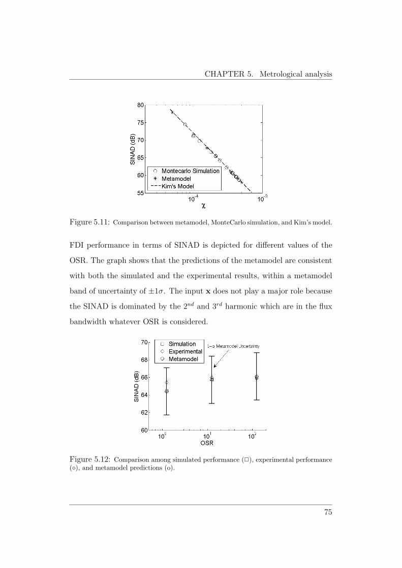
CHAPTER 5. Metrological analysis
Figure 5.11: Comparison between metamodel, MonteCarlo simulation, and Kim’s model.
FDI performance in terms of SINAD is depicted for different values of the
OSR. The graph shows that the predictions of the metamodel are consistent
with both the simulated and the experimental results, within a metamodel
band of uncertainty of ±1σ. The input x does not play a major role because
the SINAD is dominated by the 2nd and 3rd harmonic which are in the flux
bandwidth whatever OSR is considered.
Figure 5.12: Comparison among simulated performance (2), experimental performance(�), and metamodel predictions (o).
75
CHAPTER 5. Metrological analysis
5.4 Discussion
The uncertainty analytical study and preliminary numerical investigation
were aimed at addressing the challenges of the design, both at conceptual
and at physical level. The results showed that:
• a numerical on-line integration by means of trapezium (first-order filter)
is adequate to the target performance;
• an absolute UTC with a resolution of 50 ns is necessary to achieve
the FDI performance, by assuring an adequate accuracy of the passage
from time to angular domains, and, in general, to any external trigger
events;
• the flux uncertainty does not increase according to the measurement
time, owing to the presence of an absolute UTC.
• a custom PGA, with an overall distortion of 100 dB in the required
bandwidth, is sufficient to reach the target performance in flux mea-
surement.
A comprehensive performance modeling approach to simulation of digi-
tizers for metrological purposes with a systematic procedure, supported by a
crosscheck with the first experimental results, allowed the FDI model to be
defined, identified, and validated effectively over all the design and operating
conditions. The analysis outcomes showed the practical usefulness of the
proposed approach in defining the impact of uncertainty sources, working
conditions, and design configurations during a digitizer design and will be a
reference for validating future FDI upgrades. In particular, the statistical-
76
CHAPTER 5. Metrological analysis
based model confirmed that the UTC improves the FDI performance in terms
of SINAD while the integration algorithm does not play a major role on it.
Moreover, the FDI metamodel analysis pointed out that the most im-
portant distortion to be corrected is the asymmetry of the transfer function
of the acquisition chain (PGA and ADC), while the actual acquisition noise
level and the clock jitter do not deeply affect the FDI performance. The dom-
inant non-linearity of the transfer function was found to be associated with
the buffer amplifier of the ADC AD7674. This was an important indication
for the implementation of the final version of the FDI.
77
Chapter 6
Physical design andimplementation
The FDI, a 6U PXI card (Fig. 6.1), was designed according to the conceptual
architecture described in the Section 4.3. In the following, the main FDI
physical blocks, namely the front-end panel, the digitizer chain with the
PGA and the ADC, the DSP, the FPGA, and the PXI communication bus
are described by highlighting the rationale for the choice of the hardware
components.
Then, the FDI state machine is illustrated by providing details about the
DSP firmware design and the on-line measurement algorithm.
Finally, the software for the remote control of the FDI, conceived as a
part of the new Flexible Framework for Magnetic Measurement (FFMM) is
described.
6.1 The front-end panel
In Fig. 6.2, the FDI front panel is depicted. The measurement coil is con-
nected to the FDI by a 2-pin lemo differential connector (COIL IN ), or by
two one-pin lemo connector (IN+, IN-). The single-ended output of the
78
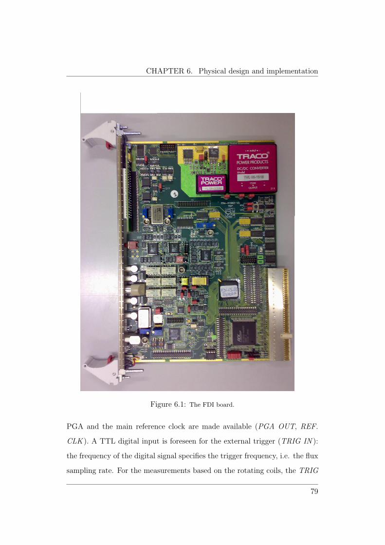
CHAPTER 6. Physical design and implementation
Figure 6.1: The FDI board.
PGA and the main reference clock are made available (PGA OUT, REF.
CLK ). A TTL digital input is foreseen for the external trigger (TRIG IN ):
the frequency of the digital signal specifies the trigger frequency, i.e. the flux
sampling rate. For the measurements based on the rotating coils, the TRIG
79
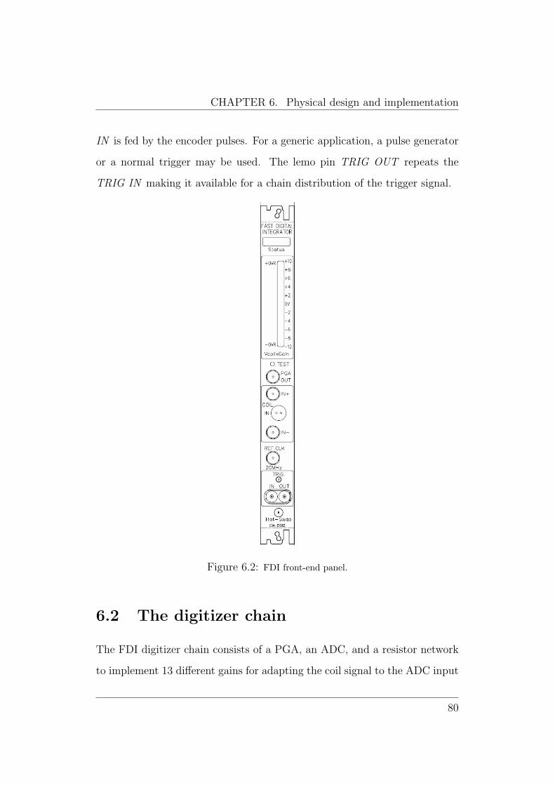
CHAPTER 6. Physical design and implementation
IN is fed by the encoder pulses. For a generic application, a pulse generator
or a normal trigger may be used. The lemo pin TRIG OUT repeats the
TRIG IN making it available for a chain distribution of the trigger signal.
Figure 6.2: FDI front-end panel.
6.2 The digitizer chain
The FDI digitizer chain consists of a PGA, an ADC, and a resistor network
to implement 13 different gains for adapting the coil signal to the ADC input
80
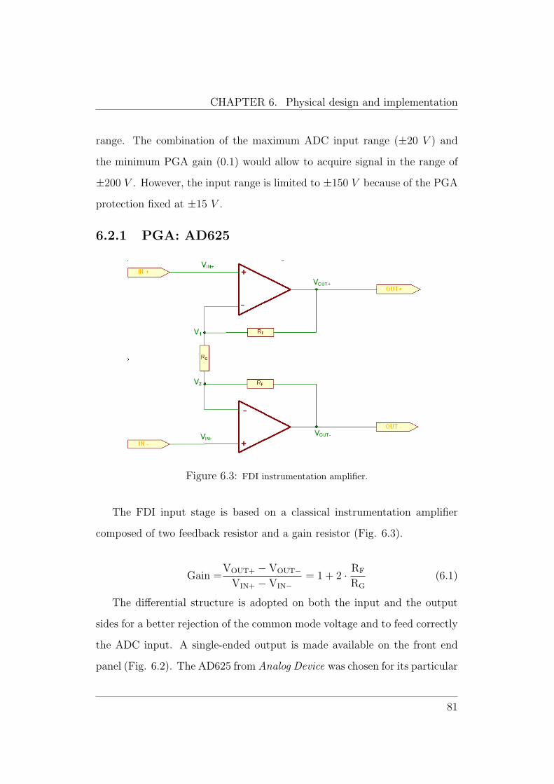
CHAPTER 6. Physical design and implementation
range. The combination of the maximum ADC input range (±20 V ) and
the minimum PGA gain (0.1) would allow to acquire signal in the range of
±200 V . However, the input range is limited to ±150 V because of the PGA
protection fixed at ±15 V .
6.2.1 PGA: AD625
Figure 6.3: FDI instrumentation amplifier.
The FDI input stage is based on a classical instrumentation amplifier
composed of two feedback resistor and a gain resistor (Fig. 6.3).
Gain =VOUT+ − VOUT−
VIN+ − VIN−= 1 + 2 · RF
RG
(6.1)
The differential structure is adopted on both the input and the output
sides for a better rejection of the common mode voltage and to feed correctly
the ADC input. A single-ended output is made available on the front end
panel (Fig. 6.2). The AD625 from Analog Device was chosen for its particular
81
CHAPTER 6. Physical design and implementation
suitability to implement a programmable gain amplifier and for its AC and
DC performance (Tab. 6.1) [87].
Gain drift 0.25 µV/◦C (max)Offset drift 5 ppm/◦C (max)
AC distortion 10 ppmNoise density at 1 kHz 4nv/
√Hz
Table 6.1: AD 625 specifications.
The range of a coil signal can be very wide from few mV up to about 100
V in case of cold measurement (1.9 K) at high magnetic field. Therefore, a
large set of gains, as well as a protection circuit, have to be implemented. A
resistive divider, with commutation controlled by relays, is needed to provide
gains lower than 1 (6.1). For the other gains, a switchable resistor network
equipped by a multiplexer is used. An example of such a structure with a
resistor network of 5 elements is given in Fig. 6.4, where Vs is the voltage
supply, and Sense and Ref represent the differential output. As a rule,
2M + 1 resistors are needed to implement M gains.
The Tab. 6.2 resumes the combination of the resistor divider and the
PGA gain necessary to obtain the FDI gain set.
6.2.2 ADC: AD7634
FDI is based on a high-rate high-resolution digital conversion of the input
signal (see 4.1) by means of a SAR converter. The SAR technology was
chosen because it provides converters at high resolution, up to 18 bit, with
sampling rate higher than 100 kS/s and an input range of ±20 V . The Σ−∆
converters can assure a higher resolution (24-bit, for 2nd order and 3rd order
Σ−∆ converters), but at a lower sampling rate (few kS/s). In some cases,
82
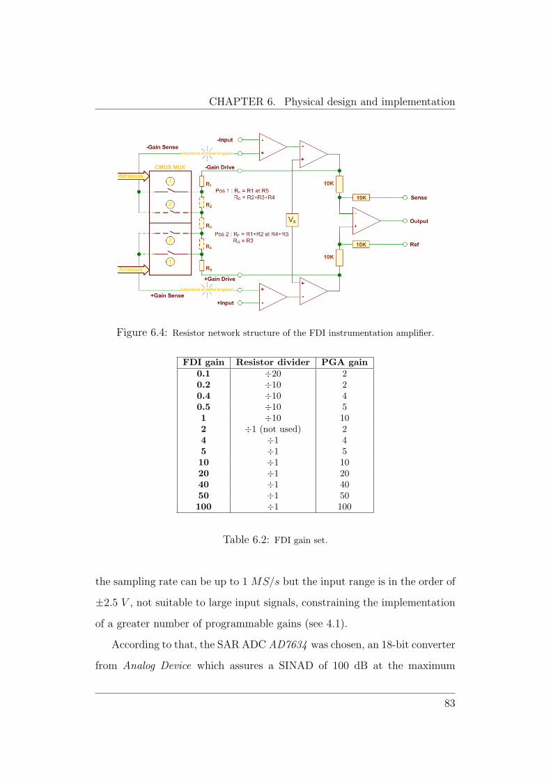
CHAPTER 6. Physical design and implementation
Figure 6.4: Resistor network structure of the FDI instrumentation amplifier.
FDI gain Resistor divider PGA gain0.1 ÷20 20.2 ÷10 20.4 ÷10 40.5 ÷10 51 ÷10 102 ÷1 (not used) 24 ÷1 45 ÷1 510 ÷1 1020 ÷1 2040 ÷1 4050 ÷1 50100 ÷1 100
Table 6.2: FDI gain set.
the sampling rate can be up to 1 MS/s but the input range is in the order of
±2.5 V , not suitable to large input signals, constraining the implementation
of a greater number of programmable gains (see 4.1).
According to that, the SAR ADC AD7634 was chosen, an 18-bit converter
from Analog Device which assures a SINAD of 100 dB at the maximum
83
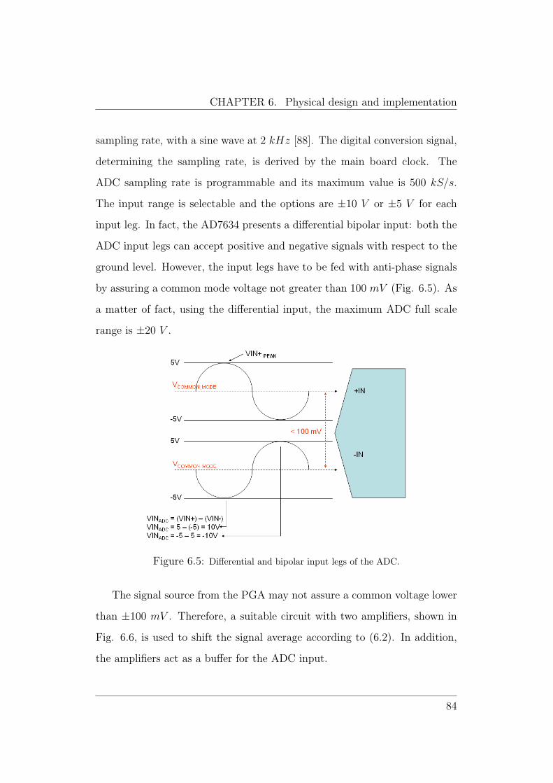
CHAPTER 6. Physical design and implementation
sampling rate, with a sine wave at 2 kHz [88]. The digital conversion signal,
determining the sampling rate, is derived by the main board clock. The
ADC sampling rate is programmable and its maximum value is 500 kS/s.
The input range is selectable and the options are ±10 V or ±5 V for each
input leg. In fact, the AD7634 presents a differential bipolar input: both the
ADC input legs can accept positive and negative signals with respect to the
ground level. However, the input legs have to be fed with anti-phase signals
by assuring a common mode voltage not greater than 100 mV (Fig. 6.5). As
a matter of fact, using the differential input, the maximum ADC full scale
range is ±20 V .
Figure 6.5: Differential and bipolar input legs of the ADC.
The signal source from the PGA may not assure a common voltage lower
than ±100 mV . Therefore, a suitable circuit with two amplifiers, shown in
Fig. 6.6, is used to shift the signal average according to (6.2). In addition,
the amplifiers act as a buffer for the ADC input.
84
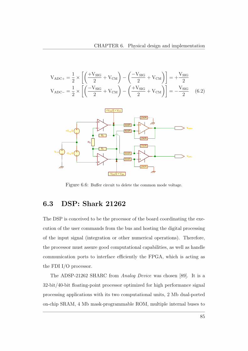
CHAPTER 6. Physical design and implementation
VADC+ =1
2×
[(+VSIG
2+ VCM
)−
(−VSIG
2+ VCM
)]= +
VSIG
2
VADC− =1
2×
[(−VSIG
2+ VCM
)−
(+VSIG
2+ VCM
)]= −VSIG
2(6.2)
Figure 6.6: Buffer circuit to delete the common mode voltage.
6.3 DSP: Shark 21262
The DSP is conceived to be the processor of the board coordinating the exe-
cution of the user commands from the bus and hosting the digital processing
of the input signal (integration or other numerical operations). Therefore,
the processor must assure good computational capabilities, as well as handle
communication ports to interface efficiently the FPGA, which is acting as
the FDI I/O processor.
The ADSP-21262 SHARC from Analog Device was chosen [89]. It is a
32-bit/40-bit floating-point processor optimized for high performance signal
processing applications with its two computational units, 2 Mb dual-ported
on-chip SRAM, 4 Mb mask-programmable ROM, multiple internal buses to
85
CHAPTER 6. Physical design and implementation
eliminate I/O bottlenecks, and an innovative digital applications interface.
Fabricated in a state-of-the art, high-speed CMOS process, the ADSP-21262
DSP achieves an instruction cycle time of 5 ns at 200 MHz. On the FDI
board, it uses a 160 MHz clock derived by the 20 MHz main clock by means
of the internal DSP PLL.
The ADSP 21262 provides a Serial Peripheral Interface (SPI) port, a 16-
bit parallel port, 4 Flag/interrupt lines, and a Digital Audio Interface (DAI),
including six serial ports, two Precision Clock Generators (PCGs), an Input
Data Port (IDP), six flag outputs and six flag inputs, and three timers.
The parallel port is used to read the ADC data, the UTC values, the
FDI internal status (FPGA status, calibration status, measurement status,
errors), and the user commands. The control signals of the parallel port are
managed by the FPGA. The SPI port is used to transfer the data processed
by the DSP. A 32-bit shift register is used for converting the SPI data to a
parallel format in order to be stocked on a 32 kB dual port RAM, imple-
mented on the FPGA, accessible on the PCI bus. The 4 flags are used as (i)
flash memory chip select for the DSP booting, (ii) FPGA or error interrupts,
(iii) data valid interrupt for reading the ADC data, (iv) SPI port chip select
for transferring the processed data.
The other peripheral ports are not used. However, they can be considered
for future FDI upgrades. In fact, the possibility of acting at low level on the
DSP peripheral ports, as well as on the FPGA, is one of the reason leading
to design a custom board.
86
CHAPTER 6. Physical design and implementation
6.4 FPGA: Spartan XC3S1000L
The FDI needs a low-level control logic unit, acting as a glue among the
different parts of the board and managing all the internal buses communica-
tion as an I/O processor. Such a function cannot be carried out by a DSP
because this chip is not conceived to manage a large number of digital I/O
lines. Therefore, a Field Programmable Gate Array (FPGA) is employed.
The FPGAs are based on a matrix of Configurable Logic Blocs (CLB),
linked by means of programmable interconnections. Each chip pin can be
configured as input, output, or bidirectional line with a specific family level
(LVTTL, LVCMOS, and so on).
For the FDI, the Spartan-3 XC3S1000 from Xilinx was chosen [90]. It
delivers 1 million system gates, 333 I/Os, 432 kbits of block RAM, digital
clock management for high-speed design and a wide range of platform fea-
tures to solve tough connectivity and embedded processing challenges. The
FPGA working frequency on the FDI board is 40 MHz.
The FPGA is responsible for:
• the ADC control and the automatic procedure for the offset and gain
calibration (see 6.4.2);
• the management of the external trigger pulses and the UTC control
logic (see 6.4.1);
• the management of the DSP SPI port, DSP parallel port, and the DSP
flag lines;
• the implementation of the FDI status register, command register, data
registers, and configuration registers used by the DSP;
87
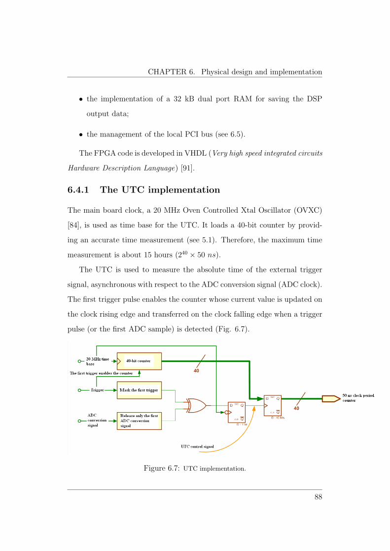
CHAPTER 6. Physical design and implementation
• the implementation of a 32 kB dual port RAM for saving the DSP
output data;
• the management of the local PCI bus (see 6.5).
The FPGA code is developed in VHDL (Very high speed integrated circuits
Hardware Description Language) [91].
6.4.1 The UTC implementation
The main board clock, a 20 MHz Oven Controlled Xtal Oscillator (OVXC)
[84], is used as time base for the UTC. It loads a 40-bit counter by provid-
ing an accurate time measurement (see 5.1). Therefore, the maximum time
measurement is about 15 hours (240 × 50 ns).
The UTC is used to measure the absolute time of the external trigger
signal, asynchronous with respect to the ADC conversion signal (ADC clock).
The first trigger pulse enables the counter whose current value is updated on
the clock rising edge and transferred on the clock falling edge when a trigger
pulse (or the first ADC sample) is detected (Fig. 6.7).
Figure 6.7: UTC implementation.
88
CHAPTER 6. Physical design and implementation
6.4.2 Offset and gain correction
The offset correction is a key issue for an integrator. In fact, the integration
of an offset voltage results in a systematic drift of the actual signal affecting
the actual values of the signal harmonics. The offset voltage depends on the
amplifier gain, thus an automatic procedure for correcting the offset voltage
and the systematic gain error was implemented by means of the FPGA by
exploiting a set of voltage references.
The FDI calibration is carried out by the following steps:
• offset voltage compensation with a short circuit at the input;
• gain error compensation;
• offset voltage compensation by means of a signal source at the input;
• saving of the gain and offset compensation parameters in a EEPROM.
The short circuit and the signal source are automatically commutated.
The offset voltage is compensated by subtracting to each ADC sample the
DC component, extracted by means of a digital filter over a time period of
about 2 s in order to delete the effects of low frequency noise.
A numerical procedure is also applied for the gain compensation. Ac-
cording to the selected gain, a suitable reference voltage is applied to the
PGA input. The ideal output is given by the absolute value of the voltage
reference multiplied by the gain. The gain correction factor is evaluated by
dividing the effective ADC samples by the expected ideal output.
The first two steps of the calibration procedure are aimed at compensating
the systematic errors of the FDI digitizer chain. Finally, the third step takes
into account the offset error introduced by the signal source resistance (i.e.
89
CHAPTER 6. Physical design and implementation
the coil resistance). The gain and offset compensation parameters are recalled
by the EEPROM each time a new gain is selected.
6.5 The PXI communication bus
The FDI is a PXI (PCI eXtensions for Instrumentation) card. PXI is a
rugged PC-based platform, combining PCI electrical-bus features with the
modular, eurocard packaging of CompactPCI, by further adding specialized
synchronization buses and key software features [92]. Such features allow PXI
bus to be widely used for PC-based measurement and automation systems
for industrial applications, as well as for scientific experiments [93], [94], [95],
[96].
The PXI/CPCI cards, usually allocated in an external rack, are the final
target of the communication chain controlled by a host unit. The host unit
can be: (i) a CPCI controller plugged in the rack; (ii) a standard PC. In
this last case, an extender kit is needed to link the host PCI bus to the PXI
bus and the final target (the PXI card) is not reached directly by the first
communication initiator (PC). The final target uses a local bus manager to
interface the PXI bus. Such a role can be implemented into an FPGA with
a custom design or can be delegated to a dedicated integrated chip.
The PXI bus architecture of the FDI is shown in Fig. 6.8. In this case
the host unit is a PC and a kit (PCI 8570 and PXI 8570, [97]) is used to
extend its PCI bus. The FDI interface with the PCI bus is handled via a
PCI bridge (PLX 9030, [98]), for programming the transactions on the local
bus by the user straight forward. The bridge between PCI and local bus
decouples the problems of FPGA design development from PCI interfacing,
leading to a design more reliable and easier to maintain. Such an architecture
90
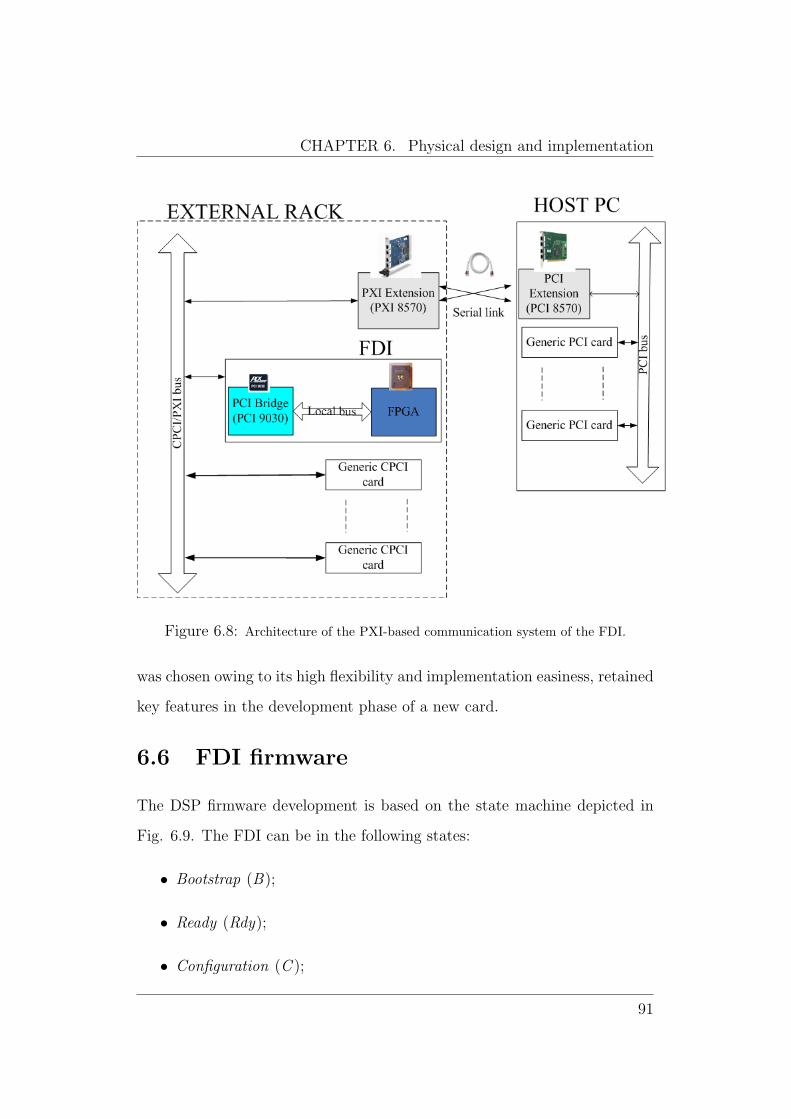
CHAPTER 6. Physical design and implementation
Figure 6.8: Architecture of the PXI-based communication system of the FDI.
was chosen owing to its high flexibility and implementation easiness, retained
key features in the development phase of a new card.
6.6 FDI firmware
The DSP firmware development is based on the state machine depicted in
Fig. 6.9. The FDI can be in the following states:
• Bootstrap (B);
• Ready (Rdy);
• Configuration (C );
91
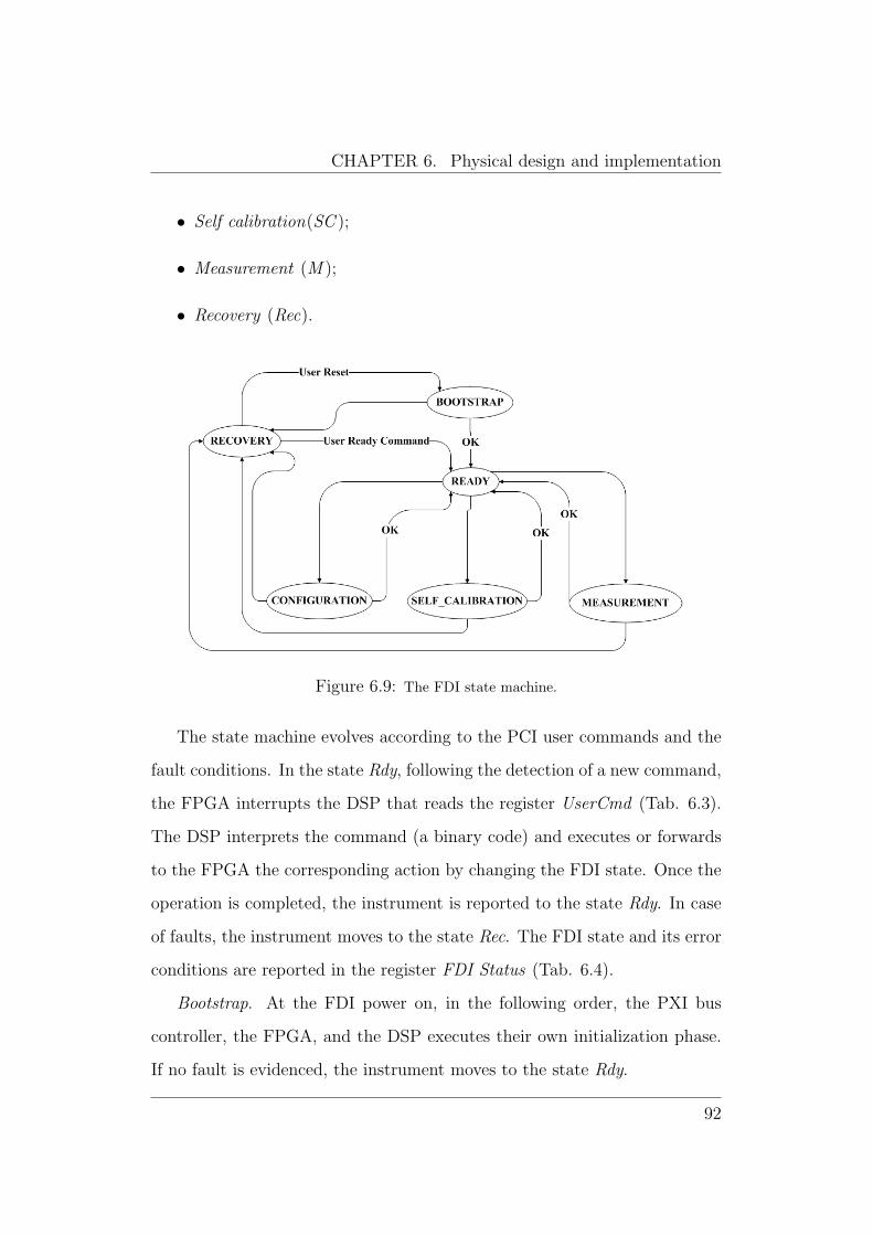
CHAPTER 6. Physical design and implementation
• Self calibration(SC );
• Measurement (M );
• Recovery (Rec).
Figure 6.9: The FDI state machine.
The state machine evolves according to the PCI user commands and the
fault conditions. In the state Rdy, following the detection of a new command,
the FPGA interrupts the DSP that reads the register UserCmd (Tab. 6.3).
The DSP interprets the command (a binary code) and executes or forwards
to the FPGA the corresponding action by changing the FDI state. Once the
operation is completed, the instrument is reported to the state Rdy. In case
of faults, the instrument moves to the state Rec. The FDI state and its error
conditions are reported in the register FDI Status (Tab. 6.4).
Bootstrap. At the FDI power on, in the following order, the PXI bus
controller, the FPGA, and the DSP executes their own initialization phase.
If no fault is evidenced, the instrument moves to the state Rdy.
92
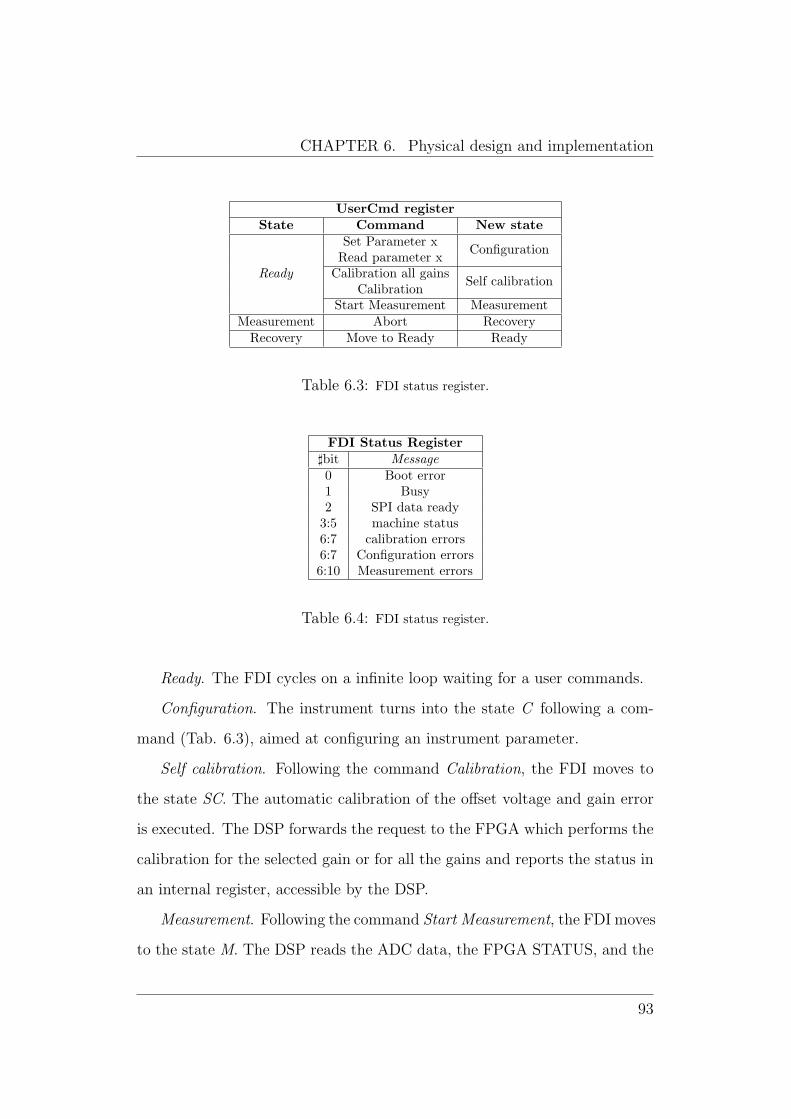
CHAPTER 6. Physical design and implementation
UserCmd registerState Command New state
Ready
Set Parameter x ConfigurationRead parameter xCalibration all gains Self calibrationCalibrationStart Measurement Measurement
Measurement Abort RecoveryRecovery Move to Ready Ready
Table 6.3: FDI status register.
FDI Status Register]bit Message0 Boot error1 Busy2 SPI data ready
3:5 machine status6:7 calibration errors6:7 Configuration errors6:10 Measurement errors
Table 6.4: FDI status register.
Ready. The FDI cycles on a infinite loop waiting for a user commands.
Configuration. The instrument turns into the state C following a com-
mand (Tab. 6.3), aimed at configuring an instrument parameter.
Self calibration. Following the command Calibration, the FDI moves to
the state SC. The automatic calibration of the offset voltage and gain error
is executed. The DSP forwards the request to the FPGA which performs the
calibration for the selected gain or for all the gains and reports the status in
an internal register, accessible by the DSP.
Measurement. Following the command Start Measurement, the FDI moves
to the state M. The DSP reads the ADC data, the FPGA STATUS, and the
93
CHAPTER 6. Physical design and implementation
UTC values. Once the data are processed, they are transferred to the Dual
port RAM to be read on the PXI bus. The instrument exits from the state
M following an Abort command (a closure procedure is foreseen), an error
condition, or the end of the measurement procedure. In the state M, the
instrument appears as busy to the user, and, thus, any command, excepting
for Abort, is not considered.
Recovery. Following an error condition, the DSP moves to the state Rec.
By knowing the previous state machine and the FPGA status, the DSP
recognizes the fault and stores a suitable code in the register FDI Status. If
the fault condition was not fatal, following the command Move to Ready, the
instrument moves to the state Rdy.
6.6.1 On-line measurement algorithm
In this Section, the on-line integration algorithm is illustrated highlighting
the procedure adopted to avoid the propagation of numerical error.
According to the FDI working principle (Fig. 4.2), the DSP releases a
flux sample at each trigger pulse by integrating on-line the coil signal. Thus,
the trigger frequency represents the flux sampling rate, whose theoretical
maximum value is limited by the ADC Nyquist frequency.
The main problem related to the on-line integration is the time constraint.
At each ADC conversion, the board processor receives an interrupt, thus it
launches a process for reading the voltage sample, computing the flux through
a suitable numerical integration, saving it into the memory, and returning the
control to the interrupted task. In an on-line process, the processed samples
have to be released at the same rate as the acquisition. Therefore, all the
above tasks, required for the flux computation and the board management,
94
CHAPTER 6. Physical design and implementation
have to be performed within one ADC sampling period τc. In spite of the
theoretical board capability of performing on-line integration at the ADC
Nyquist frequency, hardware constraints related to the trigger detection, limit
the actual flux sampling rate to half of the theoretical value. In fact, since
a trigger pulse has to be larger than two ADC sampling periods in order to
be detected, the integral results are released at a maximum rate of 1/(2τc).
The maximum sampling rate of the FDI is 500 kS/s, thus the instrument is
capable of performing a flux analysis over a Nyquist bandwidth of 125 kHz.
The actual possibility of applying on-line algorithms and, in particular, on-
line integration, was achieved by a smart management of the DSP Interrupt
Service Routines (ISR) and of the reading operation from the DSP parallel
port [99].
The uncertainty analysis proved the trapezoidal algorithm capability of
reducing the numerical integration error considerably with respect to the
rectangular algorithm, with a very low computational overhead (see 5.2).
Therefore, the trapezoidal algorithm was implemented on the DSP. It is
based on the 32-bit integer type to reduce rounding errors. The increment
flux is evaluated as a 32-bit floating point at the trigger event. The number
of multiplications of the algorithm are reduced by means of the formula:
∆ϕk =(V ∗k−1 + V1)
2· τak
+(V1 + 2V2 + ....+ 2VN−1 + VN)
2τi +
(VN + V ∗k )
2· τbk
(6.3)
where ∆ϕk is the flux increment, τi is the ADC clock, Vi are the ADC codes
sampled between two trigger events, V ∗k−1 and V ∗k are the ADC code recon-
structed by linear interpolation at the trigger event k− 1 and k respectively,
and τakand τbk
are the time interval evaluated by means of the UTC mea-
surements. The evaluation of ∆ϕk (red marked zone) is reported in Fig.
95
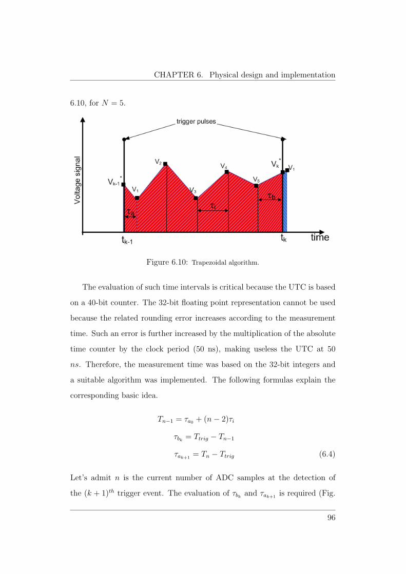
CHAPTER 6. Physical design and implementation
6.10, for N = 5.
Figure 6.10: Trapezoidal algorithm.
The evaluation of such time intervals is critical because the UTC is based
on a 40-bit counter. The 32-bit floating point representation cannot be used
because the related rounding error increases according to the measurement
time. Such an error is further increased by the multiplication of the absolute
time counter by the clock period (50 ns), making useless the UTC at 50
ns. Therefore, the measurement time was based on the 32-bit integers and
a suitable algorithm was implemented. The following formulas explain the
corresponding basic idea.
Tn−1 = τa0 + (n− 2)τi
τbk= Ttrig − Tn−1
τak+1= Tn − Ttrig (6.4)
Let’s admit n is the current number of ADC samples at the detection of
the (k + 1)th trigger event. The evaluation of τbkand τak+1
is required (Fig.
96
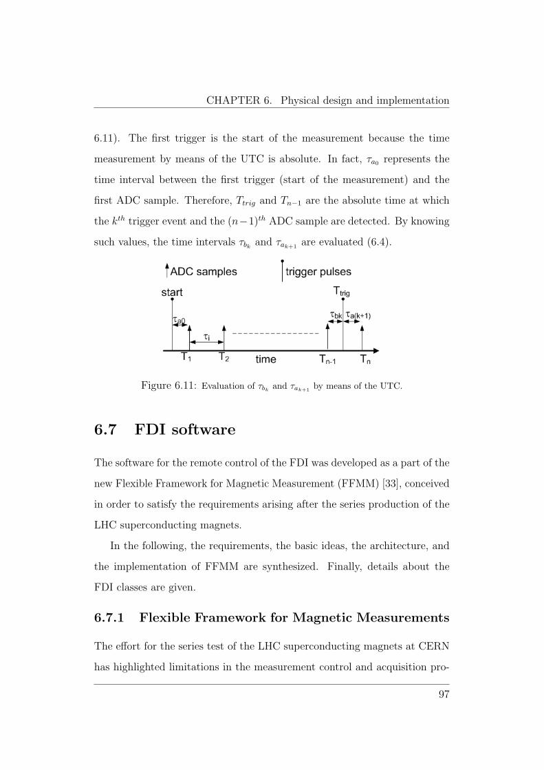
CHAPTER 6. Physical design and implementation
6.11). The first trigger is the start of the measurement because the time
measurement by means of the UTC is absolute. In fact, τa0 represents the
time interval between the first trigger (start of the measurement) and the
first ADC sample. Therefore, Ttrig and Tn−1 are the absolute time at which
the kth trigger event and the (n−1)th ADC sample are detected. By knowing
such values, the time intervals τbkand τak+1
are evaluated (6.4).
Figure 6.11: Evaluation of τbkand τak+1 by means of the UTC.
6.7 FDI software
The software for the remote control of the FDI was developed as a part of the
new Flexible Framework for Magnetic Measurement (FFMM) [33], conceived
in order to satisfy the requirements arising after the series production of the
LHC superconducting magnets.
In the following, the requirements, the basic ideas, the architecture, and
the implementation of FFMM are synthesized. Finally, details about the
FDI classes are given.
6.7.1 Flexible Framework for Magnetic Measurements
The effort for the series test of the LHC superconducting magnets at CERN
has highlighted limitations in the measurement control and acquisition pro-
97
CHAPTER 6. Physical design and implementation
grams, mainly associated with the relatively long time needed for a develop-
ment iteration (the cycle of specification-programming-debugging-validation).
In practice, the ideal situation would be to have a flexible software frame-
work [100], providing a robust library to control all the instrumentation in-
volved in the tests, as well as a flexible design to help the user-specialist
in the design of new measurement algorithm. Moreover, such a framework
has to provide an infrastructure that permits to design measurement tests
on the basis of a script provided by a test engineer who is not necessarily a
user-specialist.
At CERN, the Magnetic Measurement Program (MMP) was used in last
years to perform control and data acquisition [101]. However, the software
bears a long inheritance of the evolution from the original version of the
magnetic measurement program resulting difficult to maintain and extend.
Another interesting framework developed at CERN is the Front-End Software
Architecture framework (FESA) [102]. Although FESA is a very powerful
tool, it requires strong collaboration and involvement at the lowest software
level with the developers in order to adapt the architecture to the magnetic
measurements as it was specifically designed for the LHC control. As far as
the other research laboratories are concerned, a new software system to test
accelerator magnets, the Extensible Measurement System (EMS), has been
developed at Fermi National Accelerator Laboratory (FNAL) [103]. The
collaboration among the institutes Alba, Desy, Elettra, ESRF (European
Synchrotron Radiation Facility) and Soleil have led to the development of
an object-oriented distributed control system, TANGO [104]. To date, the
EMS framework from FNAL and the object-oriented system, TANGO, are
under development and not yet worldwide accessible to be exploited.
98
CHAPTER 6. Physical design and implementation
As far as the commercial products are concerned, a powerful framework is
provided by National Instrument, a leader firm in the field of measurement.
They propose TestStand for supporting the user in designing new test appli-
cations, by integrating software modules developed in different programming
languages (C, C + +, LabV iewTM). However, TestStand does not give a
strong support to develop single software modules.
The above discussion highlights the reasons leading to launch the devel-
opment of a new Flexible Framework for Magnetic Measurements (FFMM)
[33]. The FFMM is based on Object Oriented Programming (OOP), and
Aspect-Oriented Programming (AOP) [105]. In particular, FFMM aims at
supporting the user in developing software maximizing quality in terms of
flexibility, reusability, maintainability, and portability, without neglecting ef-
ficiency, vital in test applications.
In order to achieve the above goal, FFMM is based on the following basic
ideas [106]: (i) a set of interfaces and abstract classes constitutes a white-box
layer, allowing the user to extend the framework potential by reaching high
levels of flexibility; (ii) a set of already developed modules constitutes a black-
box layer of components to be easily reused from the framework users; such
a solution improves the parameters of code reuse, as well as the use easiness
by end users; (iii) the Aspect-Oriented Programming (AOP) improves fur-
ther the measurement software reusability and maintainability [105]: features
transversal to several modules are implemented in separates units (aspects),
in order to enhance the modularity of the system as a whole, by improv-
ing the maintainability significantly [107]; (iv) the framework can satisfy
requirements in a given application domain by a slight effort, by developing
a library of reusable modules incrementally; (v) a suitable definition of the
99
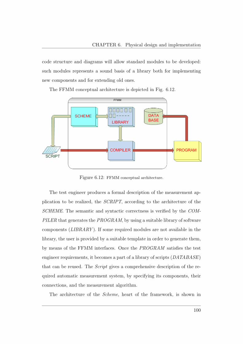
CHAPTER 6. Physical design and implementation
code structure and diagrams will allow standard modules to be developed:
such modules represents a sound basis of a library both for implementing
new components and for extending old ones.
The FFMM conceptual architecture is depicted in Fig. 6.12.
Figure 6.12: FFMM conceptual architecture.
The test engineer produces a formal description of the measurement ap-
plication to be realized, the SCRIPT, according to the architecture of the
SCHEME. The semantic and syntactic correctness is verified by the COM-
PILER that generates the PROGRAM, by using a suitable library of software
components (LIBRARY ). If some required modules are not available in the
library, the user is provided by a suitable template in order to generate them,
by means of the FFMM interfaces. Once the PROGRAM satisfies the test
engineer requirements, it becomes a part of a library of scripts (DATABASE )
that can be reused. The Script gives a comprehensive description of the re-
quired automatic measurement system, by specifying its components, their
connections, and the measurement algorithm.
The architecture of the Scheme, heart of the framework, is shown in
100
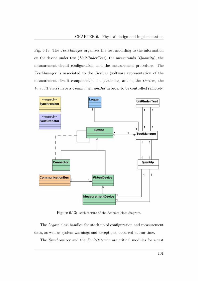
CHAPTER 6. Physical design and implementation
Fig. 6.13. The TestManager organizes the test according to the information
on the device under test (UnitUnderTest), the measurands (Quantity), the
measurement circuit configuration, and the measurement procedure. The
TestManager is associated to the Devices (software representation of the
measurement circuit components). In particular, among the Devices, the
VirtualDevices have a CommunicationBus in order to be controlled remotely.
Figure 6.13: Architecture of the Scheme: class diagram.
The Logger class handles the stock up of configuration and measurement
data, as well as system warnings and exceptions, occurred at run-time.
The Synchronizer and the FaultDetector are critical modules for a test
101
CHAPTER 6. Physical design and implementation
application: the former allows the measurement algorithm timing, while the
latter fosters the identification and the location of failures and faults, trans-
parently to the user. Such features are transversal to several functional units
(cross-cutting concerns), and thus they are encapsulated by means of aspects,
according to the AOP approach [107], [108]: the fault management strategy
and the software synchronization policy are extrapolated by the related sin-
gle classes and treated separately. In this way, future modifications related
to these topics will affect only the Synchronizer and the FaultDetector mod-
ules, without involving all the classes related, directly or indirectly, to the
fault or synchronization events. The main advantage of such a technique
is the maintainability and the reusability of the code. For each new device
added to the station, the related synchronization and fault detection code
are added to the aspect hierarchy. As a consequence, the AOP design, with
respect to ’traditional’ OOP version, exhibits a better modularized design
by eliminating code scattering and tangling, and increasing the possibility of
code reuse.
The core part of FFMM, the Scheme (Fig. 6.13), was implemented in
C++, by identifying the most suitable design patterns for generic measure-
ment procedures [109], [33].
6.7.2 FDI classes
Inside FFMM, FDI is a Virtual Device (Fig. 6.13) to which the PCI Com-
munication bus is associated for the remote control of the instrument. The
access on the bus and the basic read/write operations are based on the Ap-
plication Programming Interface (API) functions provided by PLX. The FDI
programming functions, organized as methods of the C++ class FastDI, per-
102
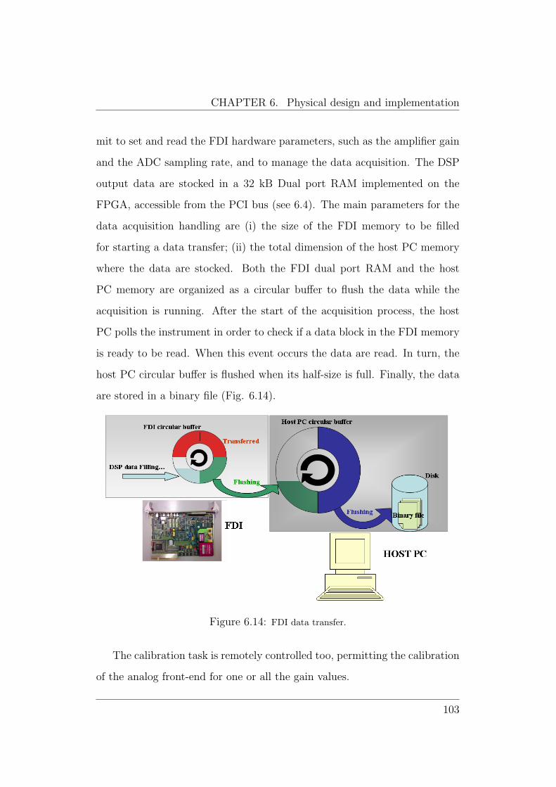
CHAPTER 6. Physical design and implementation
mit to set and read the FDI hardware parameters, such as the amplifier gain
and the ADC sampling rate, and to manage the data acquisition. The DSP
output data are stocked in a 32 kB Dual port RAM implemented on the
FPGA, accessible from the PCI bus (see 6.4). The main parameters for the
data acquisition handling are (i) the size of the FDI memory to be filled
for starting a data transfer; (ii) the total dimension of the host PC memory
where the data are stocked. Both the FDI dual port RAM and the host
PC memory are organized as a circular buffer to flush the data while the
acquisition is running. After the start of the acquisition process, the host
PC polls the instrument in order to check if a data block in the FDI memory
is ready to be read. When this event occurs the data are read. In turn, the
host PC circular buffer is flushed when its half-size is full. Finally, the data
are stored in a binary file (Fig. 6.14).
Figure 6.14: FDI data transfer.
The calibration task is remotely controlled too, permitting the calibration
of the analog front-end for one or all the gain values.
103
CHAPTER 6. Physical design and implementation
In case of faults, the FDI moves to the Recovery state (6.6). The reading
of the instrument status allows checking the fault condition. If the error
condition was removed at DSP firmware level the instrument is sent to the
Ready state by a suitable command, otherwise a reset command is foreseen.
The class FDICluster was developed since many measurement applica-
tions require a multi-channel acquisition. It manages a cluster of n FDI that
are involved in the same acquisition task. As far as the set/read methods are
concerned, the cluster is deeply based on the methods of the class FastDI. As
far as the acquisition methods, FDICluster handles the n FDIs as a unique
multi-channel board optimizing the reading time. In fact, the process fore-
sees an unique polling phase for all the elements of the cluster followed by a
reading scan of the boards. Such a structure permits to read out the data
from the FDIs without causing error conditions due to the buffer overwrite.
104
Chapter 7
Metrological and throughputrate characterization
A measurement station is equipped in order to verify metrological and through-
out performance of FDI.
In metrological characterization, FDI performance, working as a digitizer
and as an integrator, is assessed by means of static, dynamic, and timebase
tests.
Metrological static tests point out the Differential Non Linearity (DNL)
of the digitizer chain [34] and the integral transfer function non-linearity of
the instrument, working in integrator mode.
Metrological dynamic tests, based on the FFT analysis, aim at evaluating
the SIgnal to Noise and Distortion (SINAD) and the Signal Non Harmonic
Distortion (SNHD) according to [34].
Metrological time base tests verify the numerical error of the UTC mea-
surement algorithm (see 6.4.1) to prove its actual resolution of 50 ns.
The actual throughput rate is measured by analyzing the PXI bus archi-
tecture.
Finally, the resulting FDI specifications are issued.
105
CHAPTER 7. Metrological and throughput rate characterization
7.1 Metrological characterization
In the following, (i) the measurement station and characterization strategy,
(ii) static tests, (iii) dynamic tests, and (iv) time base tests are described.
7.1.1 Measurement station and characterization strat-egy
Metrological tests are carried out by using the following instruments:
• the DC calibrator DATRON 4000A for static tests;
• the ultra-low distortion function generator Stanford DS360 for dynamic
tests;
• the function generator TTi TG1010 for providing the external trigger
pulses.
Software applications for the remote control of the measurement station
and the data analysis tools were developed in LabviewTM and MATLABTM ,
respectively.
For the sake of the comparison, both static and dynamic tests are also
performed on the PDI, representing the de-facto benchmark for magnetic
measurements. In particular, DNL and dynamic performance of both the
FDI and the PDI are compared.
PDI is intrinsically an integrator, nonetheless it works also as an ADC
(see 2.2.1). In fact, PDI is based on a first-order modulator, i.e. a voltage-
to-frequency converter. The digital voltage output V
V =n · VV FCmax
tm · fV FCmax
(7.1)
106
CHAPTER 7. Metrological and throughput rate characterization
(where n is the output number of counts at the output for a clock frequency
fV FCmax , in a measurement time tm, and VV FCmax the full scale voltage of the
instrument) can be evaluated by knowing tm, the reciprocal of the trigger
frequency, i.e. the PDI sampling rate. The trigger frequency is inversely
proportional to the PDI resolution. Conversely, the FDI measurement chain
is a waveform digitizer intrinsically, whose resolution does not depend on
the sampling rate. Therefore, DNL and dynamic tests are carried out in
comparison to PDI, working as digitizer and as integrator.
7.1.2 Static tests
In static conditions, tests for (i) DNL of the FDI digitizer chain, (ii) calibra-
tion, (iii) stability, (iv) and repeatability are carried out.
DNL of the FDI digitizer chain
The DC input signal is supplied by the DC calibrator DATRON 4000, while
the external trigger pulses for the PDI test by the function generator TTI.
With a theoretical number of 18 bits, FDI has an LSB of about 76 µV,
over an input range of ±10 V , for a total number of 262143 transition levels.
This number is very large and the complete test would take a very long time,
thus the DNL is computed on several groups of transition levels, suitably
chosen along the overall input range. In this way, the DNL is assessed in
local parts of the input range.
The number of bits and the LSB of the PDI are function of the trigger
frequency. For the static test, a trigger frequency of 512 Hz is chosen, being
a typical working condition. Therefore, the PDI LSB is 10.24 mV and the
theoretical number of bit is equal to 9.93, for a total number of transition
107
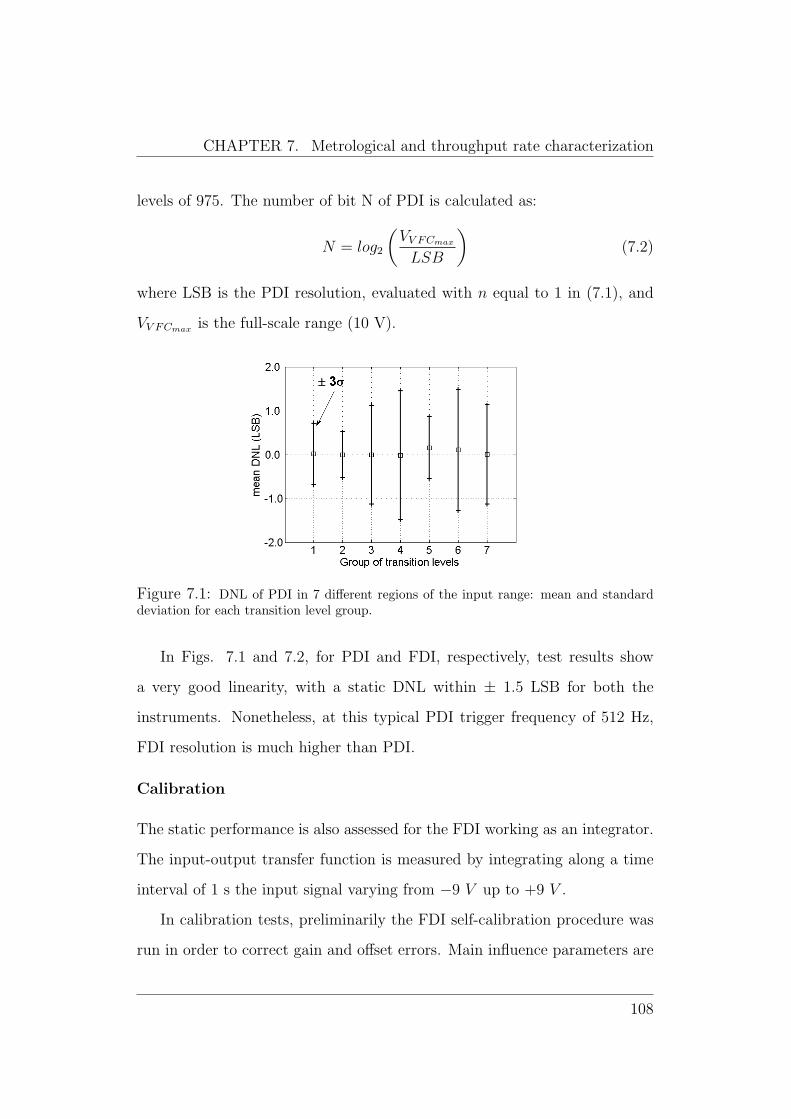
CHAPTER 7. Metrological and throughput rate characterization
levels of 975. The number of bit N of PDI is calculated as:
N = log2
(VV FCmax
LSB
)(7.2)
where LSB is the PDI resolution, evaluated with n equal to 1 in (7.1), and
VV FCmax is the full-scale range (10 V).
Figure 7.1: DNL of PDI in 7 different regions of the input range: mean and standarddeviation for each transition level group.
In Figs. 7.1 and 7.2, for PDI and FDI, respectively, test results show
a very good linearity, with a static DNL within ± 1.5 LSB for both the
instruments. Nonetheless, at this typical PDI trigger frequency of 512 Hz,
FDI resolution is much higher than PDI.
Calibration
The static performance is also assessed for the FDI working as an integrator.
The input-output transfer function is measured by integrating along a time
interval of 1 s the input signal varying from −9 V up to +9 V .
In calibration tests, preliminarily the FDI self-calibration procedure was
run in order to correct gain and offset errors. Main influence parameters are
108
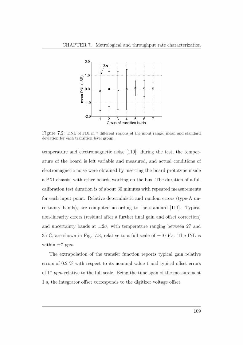
CHAPTER 7. Metrological and throughput rate characterization
Figure 7.2: DNL of FDI in 7 different regions of the input range: mean and standarddeviation for each transition level group.
temperature and electromagnetic noise [110]: during the test, the temper-
ature of the board is left variable and measured, and actual conditions of
electromagnetic noise were obtained by inserting the board prototype inside
a PXI chassis, with other boards working on the bus. The duration of a full
calibration test duration is of about 30 minutes with repeated measurements
for each input point. Relative deterministic and random errors (type-A un-
certainty bands), are computed according to the standard [111]. Typical
non-linearity errors (residual after a further final gain and offset correction)
and uncertainty bands at ±2σ, with temperature ranging between 27 and
35 C, are shown in Fig. 7.3, relative to a full scale of ±10 V s. The INL is
within ±7 ppm.
The extrapolation of the transfer function reports typical gain relative
errors of 0.2 % with respect to its nominal value 1 and typical offset errors
of 17 ppm relative to the full scale. Being the time span of the measurement
1 s, the integrator offset corresponds to the digitizer voltage offset.
109
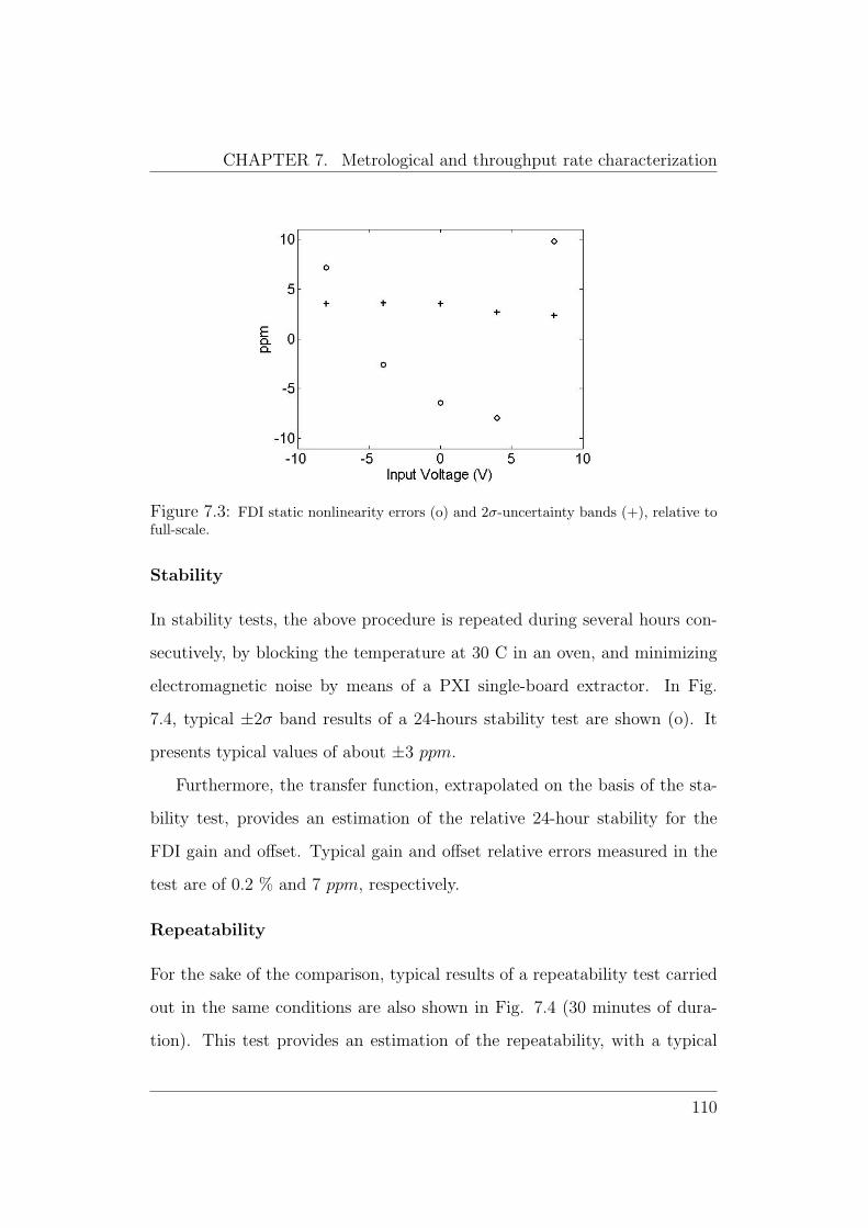
CHAPTER 7. Metrological and throughput rate characterization
Figure 7.3: FDI static nonlinearity errors (o) and 2σ-uncertainty bands (+), relative tofull-scale.
Stability
In stability tests, the above procedure is repeated during several hours con-
secutively, by blocking the temperature at 30 C in an oven, and minimizing
electromagnetic noise by means of a PXI single-board extractor. In Fig.
7.4, typical ±2σ band results of a 24-hours stability test are shown (o). It
presents typical values of about ±3 ppm.
Furthermore, the transfer function, extrapolated on the basis of the sta-
bility test, provides an estimation of the relative 24-hour stability for the
FDI gain and offset. Typical gain and offset relative errors measured in the
test are of 0.2 % and 7 ppm, respectively.
Repeatability
For the sake of the comparison, typical results of a repeatability test carried
out in the same conditions are also shown in Fig. 7.4 (30 minutes of dura-
tion). This test provides an estimation of the repeatability, with a typical
110
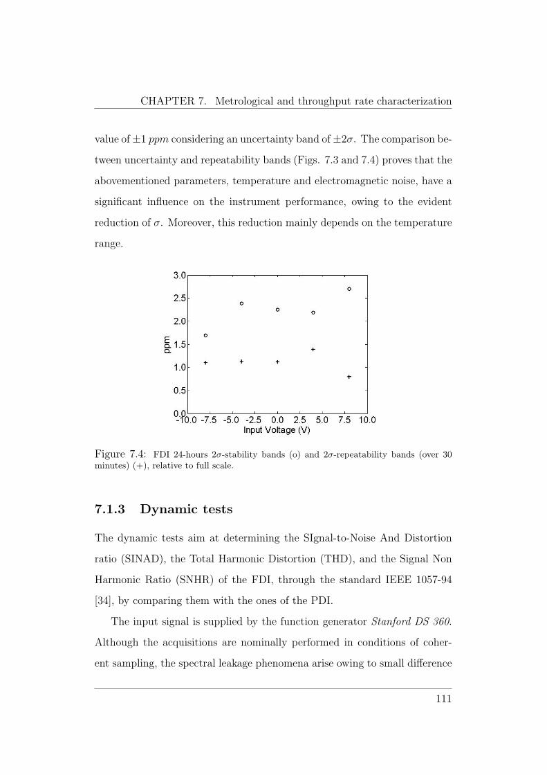
CHAPTER 7. Metrological and throughput rate characterization
value of±1 ppm considering an uncertainty band of±2σ. The comparison be-
tween uncertainty and repeatability bands (Figs. 7.3 and 7.4) proves that the
abovementioned parameters, temperature and electromagnetic noise, have a
significant influence on the instrument performance, owing to the evident
reduction of σ. Moreover, this reduction mainly depends on the temperature
range.
Figure 7.4: FDI 24-hours 2σ-stability bands (o) and 2σ-repeatability bands (over 30minutes) (+), relative to full scale.
7.1.3 Dynamic tests
The dynamic tests aim at determining the SIgnal-to-Noise And Distortion
ratio (SINAD), the Total Harmonic Distortion (THD), and the Signal Non
Harmonic Ratio (SNHR) of the FDI, through the standard IEEE 1057-94
[34], by comparing them with the ones of the PDI.
The input signal is supplied by the function generator Stanford DS 360.
Although the acquisitions are nominally performed in conditions of coher-
ent sampling, the spectral leakage phenomena arise owing to small difference
111
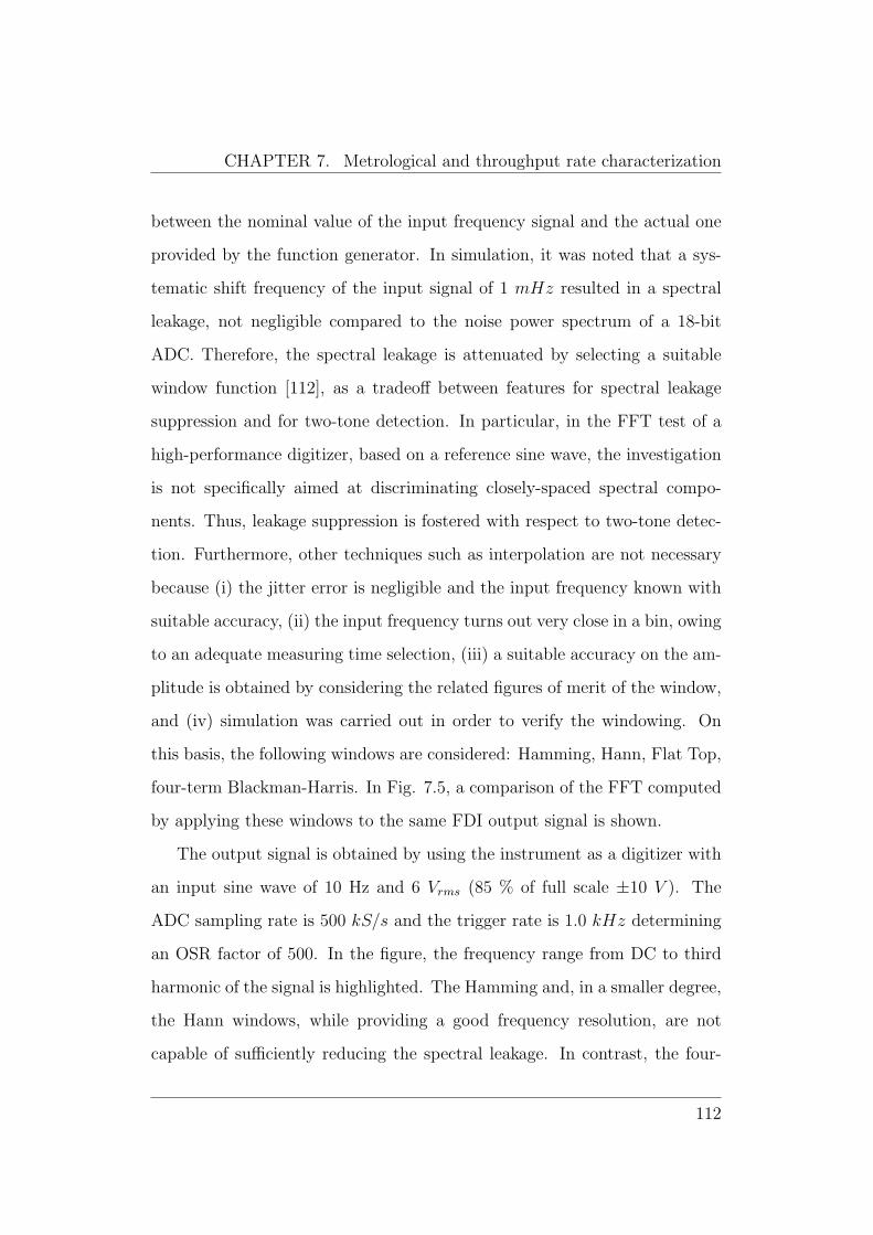
CHAPTER 7. Metrological and throughput rate characterization
between the nominal value of the input frequency signal and the actual one
provided by the function generator. In simulation, it was noted that a sys-
tematic shift frequency of the input signal of 1 mHz resulted in a spectral
leakage, not negligible compared to the noise power spectrum of a 18-bit
ADC. Therefore, the spectral leakage is attenuated by selecting a suitable
window function [112], as a tradeoff between features for spectral leakage
suppression and for two-tone detection. In particular, in the FFT test of a
high-performance digitizer, based on a reference sine wave, the investigation
is not specifically aimed at discriminating closely-spaced spectral compo-
nents. Thus, leakage suppression is fostered with respect to two-tone detec-
tion. Furthermore, other techniques such as interpolation are not necessary
because (i) the jitter error is negligible and the input frequency known with
suitable accuracy, (ii) the input frequency turns out very close in a bin, owing
to an adequate measuring time selection, (iii) a suitable accuracy on the am-
plitude is obtained by considering the related figures of merit of the window,
and (iv) simulation was carried out in order to verify the windowing. On
this basis, the following windows are considered: Hamming, Hann, Flat Top,
four-term Blackman-Harris. In Fig. 7.5, a comparison of the FFT computed
by applying these windows to the same FDI output signal is shown.
The output signal is obtained by using the instrument as a digitizer with
an input sine wave of 10 Hz and 6 Vrms (85 % of full scale ±10 V ). The
ADC sampling rate is 500 kS/s and the trigger rate is 1.0 kHz determining
an OSR factor of 500. In the figure, the frequency range from DC to third
harmonic of the signal is highlighted. The Hamming and, in a smaller degree,
the Hann windows, while providing a good frequency resolution, are not
capable of sufficiently reducing the spectral leakage. In contrast, the four-
112
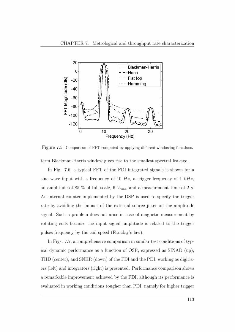
CHAPTER 7. Metrological and throughput rate characterization
Figure 7.5: Comparison of FFT computed by applying different windowing functions.
term Blackman-Harris window gives rise to the smallest spectral leakage.
In Fig. 7.6, a typical FFT of the FDI integrated signals is shown for a
sine wave input with a frequency of 10 Hz, a trigger frequency of 1 kHz,
an amplitude of 85 % of full scale, 6 Vrms, and a measurement time of 2 s.
An internal counter implemented by the DSP is used to specify the trigger
rate by avoiding the impact of the external source jitter on the amplitude
signal. Such a problem does not arise in case of magnetic measurement by
rotating coils because the input signal amplitude is related to the trigger
pulses frequency by the coil speed (Faraday’s law).
In Figs. 7.7, a comprehensive comparison in similar test conditions of typ-
ical dynamic performance as a function of OSR, expressed as SINAD (up),
THD (center), and SNHR (down) of the FDI and the PDI, working as digitiz-
ers (left) and integrators (right) is presented. Performance comparison shows
a remarkable improvement achieved by the FDI, although its performance is
evaluated in working conditions tougher than PDI, namely for higher trigger
113
CHAPTER 7. Metrological and throughput rate characterization
Figure 7.6: FFT of the signal integrated by the FDI.
frequencies, not accessible to PDI. In particular, the FDI allows SINAD to
be improved typically by about 40 dB, for the integrator working mode, and
about 35 dB, for the digitizer working mode, in comparison to the PDI.
Furthermore, the comparison between SINAD and SNHR trends shows
a clear performance improvement at increasing OSR when the instruments
are used as digitizer. The advantage deriving from over-sampling is less
evident for the integrators, likely because of the signal filtering performed
by the integral. Further, the THD shows the remarkable reduction of the
harmonic distortion, obtained by the FDI with respect to the PDI. Finally, a
comparison between SINAD and THD for the FDI, both as digitizer and as
integrator, shows that harmonic distortion is predominating and a suitable
filtering may bring to a further performance improvement of about 10 dB.
7.1.4 Time base tests
The UTC is based on a 40-bit counter implementing a fine time base with a
resolution of 50 ns (see 6.4.1). The absolute time base permits to evaluate
114
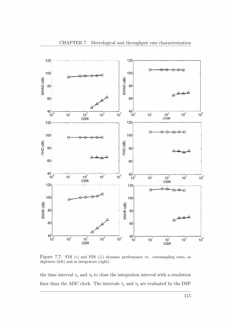
CHAPTER 7. Metrological and throughput rate characterization
Figure 7.7: FDI (◦) and PDI (4) dynamic performance vs. oversampling ratio, asdigitizers (left) and as integrators (right).
the time interval τa and τb to close the integration interval with a resolution
finer than the ADC clock. The intervals τa and τb are evaluated by the DSP
115
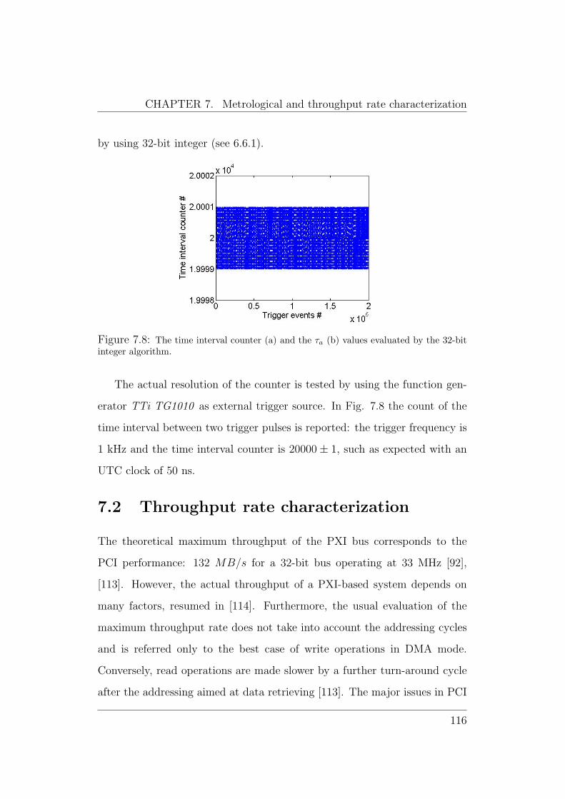
CHAPTER 7. Metrological and throughput rate characterization
by using 32-bit integer (see 6.6.1).
Figure 7.8: The time interval counter (a) and the τa (b) values evaluated by the 32-bitinteger algorithm.
The actual resolution of the counter is tested by using the function gen-
erator TTi TG1010 as external trigger source. In Fig. 7.8 the count of the
time interval between two trigger pulses is reported: the trigger frequency is
1 kHz and the time interval counter is 20000 ± 1, such as expected with an
UTC clock of 50 ns.
7.2 Throughput rate characterization
The theoretical maximum throughput of the PXI bus corresponds to the
PCI performance: 132 MB/s for a 32-bit bus operating at 33 MHz [92],
[113]. However, the actual throughput of a PXI-based system depends on
many factors, resumed in [114]. Furthermore, the usual evaluation of the
maximum throughput rate does not take into account the addressing cycles
and is referred only to the best case of write operations in DMA mode.
Conversely, read operations are made slower by a further turn-around cycle
after the addressing aimed at data retrieving [113]. The major issues in PCI
116
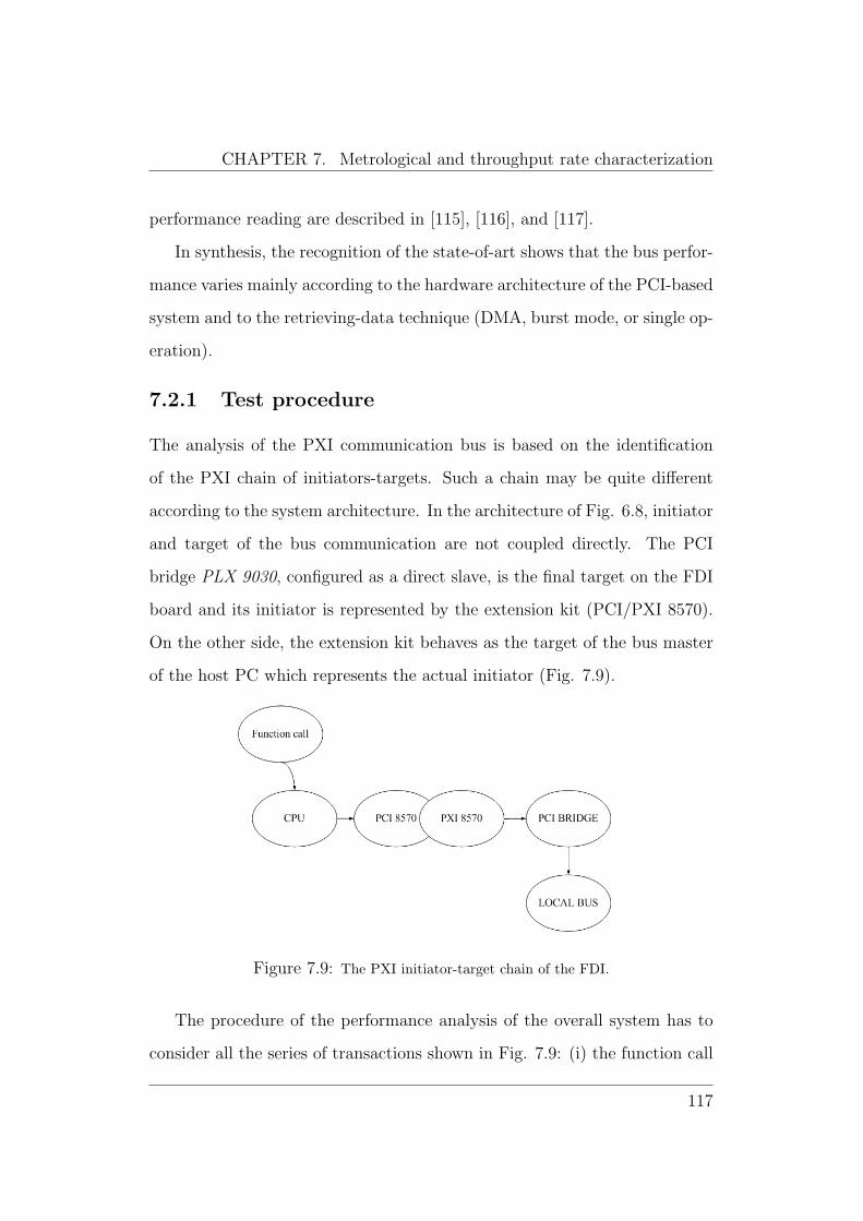
CHAPTER 7. Metrological and throughput rate characterization
performance reading are described in [115], [116], and [117].
In synthesis, the recognition of the state-of-art shows that the bus perfor-
mance varies mainly according to the hardware architecture of the PCI-based
system and to the retrieving-data technique (DMA, burst mode, or single op-
eration).
7.2.1 Test procedure
The analysis of the PXI communication bus is based on the identification
of the PXI chain of initiators-targets. Such a chain may be quite different
according to the system architecture. In the architecture of Fig. 6.8, initiator
and target of the bus communication are not coupled directly. The PCI
bridge PLX 9030, configured as a direct slave, is the final target on the FDI
board and its initiator is represented by the extension kit (PCI/PXI 8570).
On the other side, the extension kit behaves as the target of the bus master
of the host PC which represents the actual initiator (Fig. 7.9).
Figure 7.9: The PXI initiator-target chain of the FDI.
The procedure of the performance analysis of the overall system has to
consider all the series of transactions shown in Fig. 7.9: (i) the function call
117
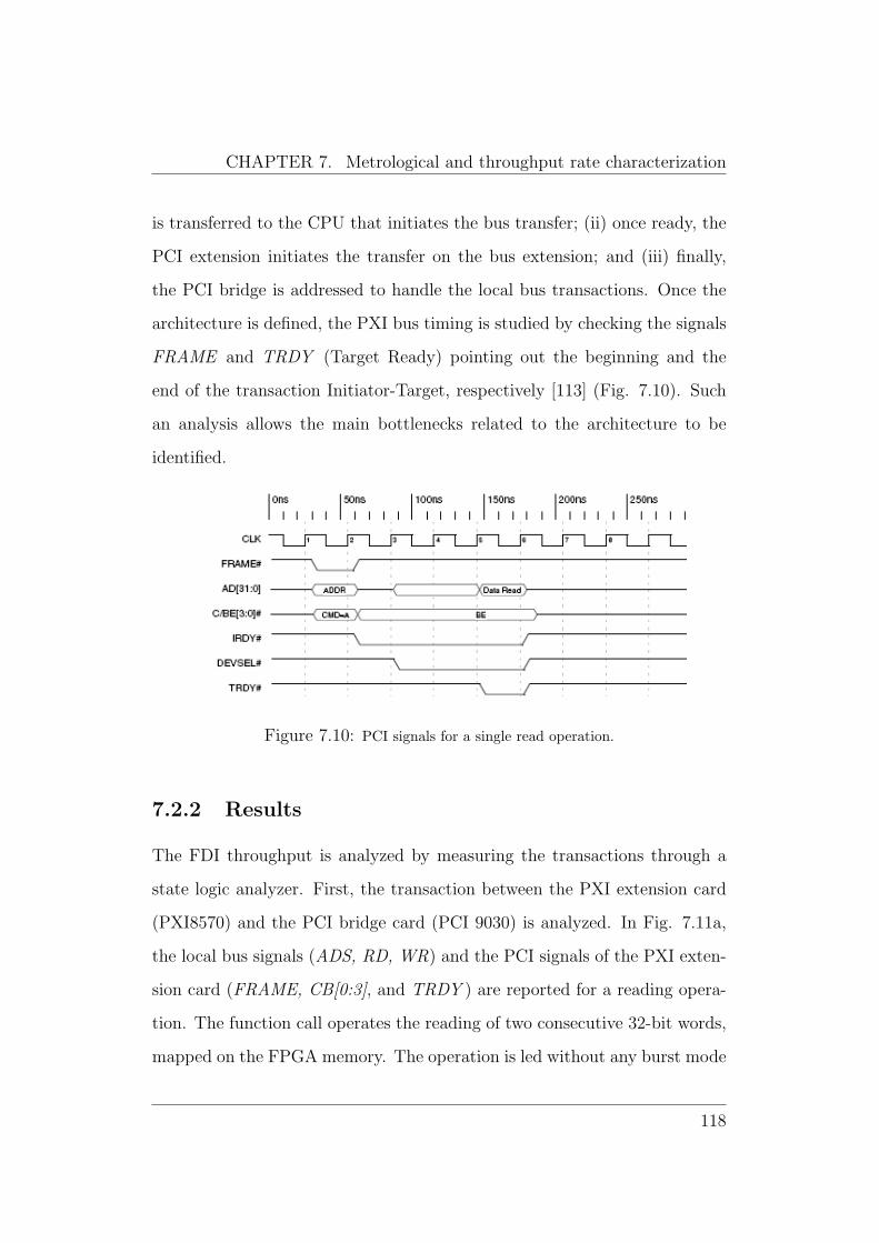
CHAPTER 7. Metrological and throughput rate characterization
is transferred to the CPU that initiates the bus transfer; (ii) once ready, the
PCI extension initiates the transfer on the bus extension; and (iii) finally,
the PCI bridge is addressed to handle the local bus transactions. Once the
architecture is defined, the PXI bus timing is studied by checking the signals
FRAME and TRDY (Target Ready) pointing out the beginning and the
end of the transaction Initiator-Target, respectively [113] (Fig. 7.10). Such
an analysis allows the main bottlenecks related to the architecture to be
identified.
Figure 7.10: PCI signals for a single read operation.
7.2.2 Results
The FDI throughput is analyzed by measuring the transactions through a
state logic analyzer. First, the transaction between the PXI extension card
(PXI8570) and the PCI bridge card (PCI 9030) is analyzed. In Fig. 7.11a,
the local bus signals (ADS, RD, WR) and the PCI signals of the PXI exten-
sion card (FRAME, CB[0:3], and TRDY ) are reported for a reading opera-
tion. The function call operates the reading of two consecutive 32-bit words,
mapped on the FPGA memory. The operation is led without any burst mode
118
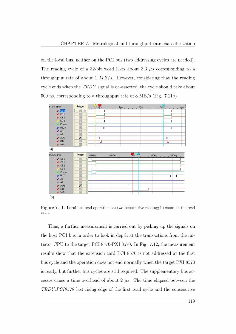
CHAPTER 7. Metrological and throughput rate characterization
on the local bus, neither on the PCI bus (two addressing cycles are needed).
The reading cycle of a 32-bit word lasts about 3.3 µs corresponding to a
throughput rate of about 1 MB/s. However, considering that the reading
cycle ends when the TRDY signal is de-asserted, the cycle should take about
500 ns, corresponding to a throughput rate of 8 MB/s (Fig. 7.11b).
Figure 7.11: Local bus read operation: a) two consecutive reading; b) zoom on the readcycle.
Thus, a further measurement is carried out by picking up the signals on
the host PCI bus in order to look in depth at the transactions from the ini-
tiator CPU to the target PCI 8570-PXI 8570. In Fig. 7.12, the measurement
results show that the extension card PCI 8570 is not addressed at the first
bus cycle and the operation does not end normally when the target PXI 8570
is ready, but further bus cycles are still required. The supplementary bus ac-
cesses cause a time overhead of about 2 µs. The time elapsed between the
TRDY PCI8570 last rising edge of the first read cycle and the consecutive
119
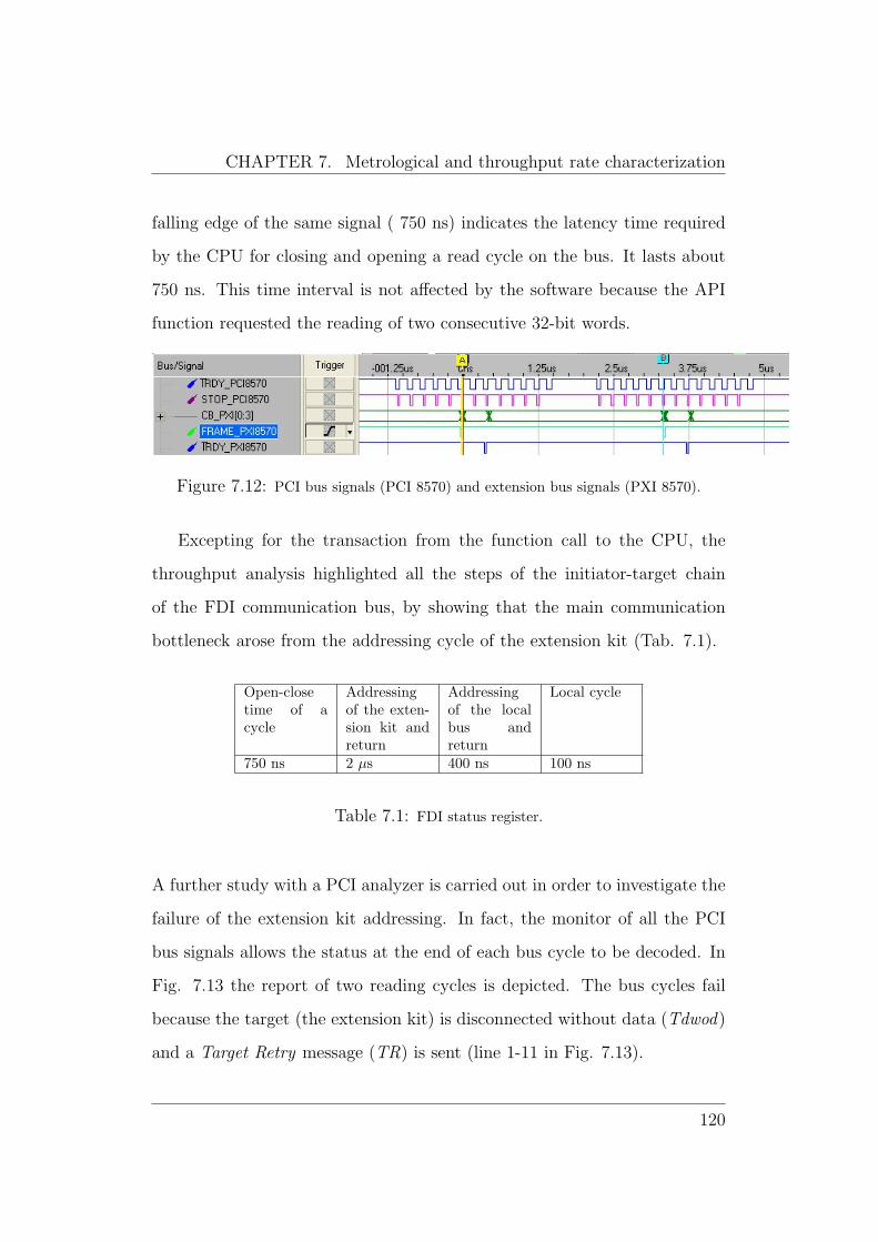
CHAPTER 7. Metrological and throughput rate characterization
falling edge of the same signal ( 750 ns) indicates the latency time required
by the CPU for closing and opening a read cycle on the bus. It lasts about
750 ns. This time interval is not affected by the software because the API
function requested the reading of two consecutive 32-bit words.
Figure 7.12: PCI bus signals (PCI 8570) and extension bus signals (PXI 8570).
Excepting for the transaction from the function call to the CPU, the
throughput analysis highlighted all the steps of the initiator-target chain
of the FDI communication bus, by showing that the main communication
bottleneck arose from the addressing cycle of the extension kit (Tab. 7.1).
Open-closetime of acycle
Addressingof the exten-sion kit andreturn
Addressingof the localbus andreturn
Local cycle
750 ns 2 µs 400 ns 100 ns
Table 7.1: FDI status register.
A further study with a PCI analyzer is carried out in order to investigate the
failure of the extension kit addressing. In fact, the monitor of all the PCI
bus signals allows the status at the end of each bus cycle to be decoded. In
Fig. 7.13 the report of two reading cycles is depicted. The bus cycles fail
because the target (the extension kit) is disconnected without data (Tdwod)
and a Target Retry message (TR) is sent (line 1-11 in Fig. 7.13).
120
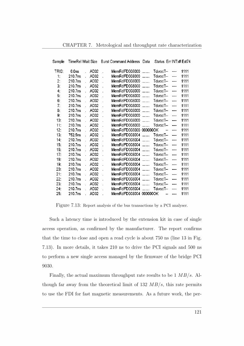
CHAPTER 7. Metrological and throughput rate characterization
Figure 7.13: Report analysis of the bus transactions by a PCI analyser.
Such a latency time is introduced by the extension kit in case of single
access operation, as confirmed by the manufacturer. The report confirms
that the time to close and open a read cycle is about 750 ns (line 13 in Fig.
7.13). In more details, it takes 210 ns to drive the PCI signals and 500 ns
to perform a new single access managed by the firmware of the bridge PCI
9030.
Finally, the actual maximum throughput rate results to be 1 MB/s. Al-
though far away from the theoretical limit of 132 MB/s, this rate permits
to use the FDI for fast magnetic measurements. As a future work, the per-
121
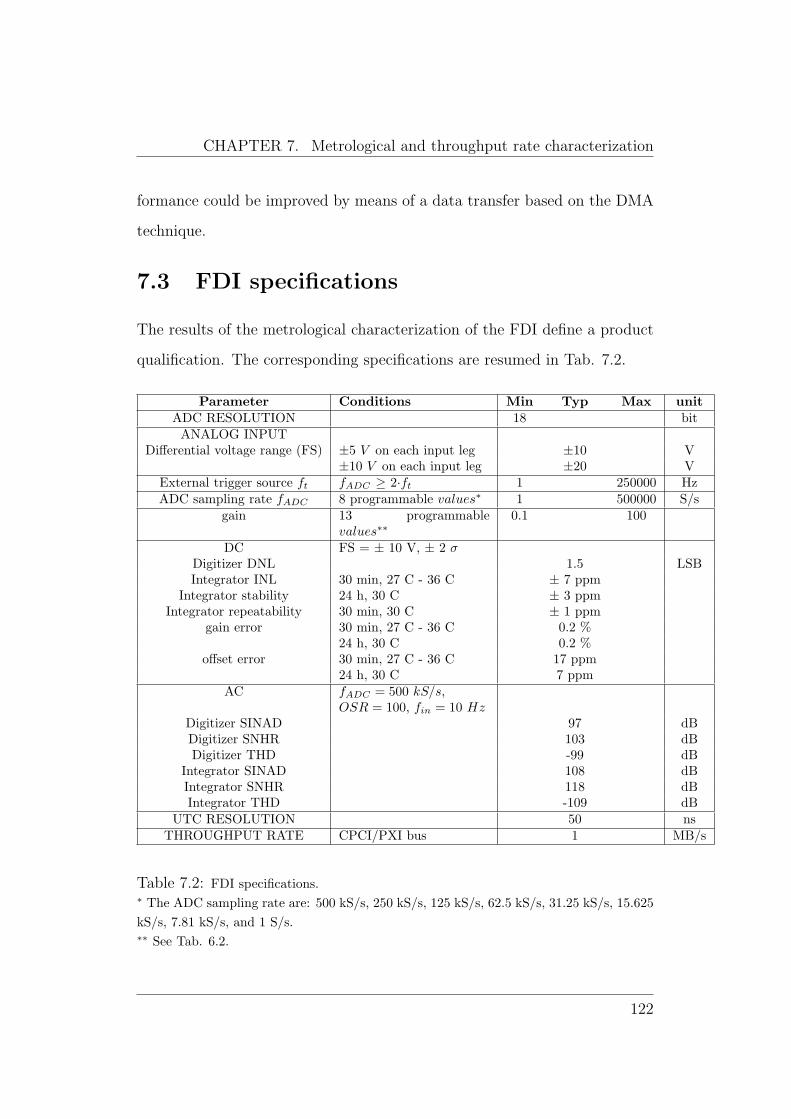
CHAPTER 7. Metrological and throughput rate characterization
formance could be improved by means of a data transfer based on the DMA
technique.
7.3 FDI specifications
The results of the metrological characterization of the FDI define a product
qualification. The corresponding specifications are resumed in Tab. 7.2.
Parameter Conditions Min Typ Max unitADC RESOLUTION 18 bitANALOG INPUT
Differential voltage range (FS) ±5 V on each input leg ±10 V±10 V on each input leg ±20 V
External trigger source ft fADC ≥ 2·ft 1 250000 HzADC sampling rate fADC 8 programmable values∗ 1 500000 S/s
gain 13 programmablevalues∗∗
0.1 100
DC FS = ± 10 V, ± 2 σDigitizer DNL 1.5 LSBIntegrator INL 30 min, 27 C - 36 C ± 7 ppm
Integrator stability 24 h, 30 C ± 3 ppmIntegrator repeatability 30 min, 30 C ± 1 ppm
gain error 30 min, 27 C - 36 C 0.2 %24 h, 30 C 0.2 %
offset error 30 min, 27 C - 36 C 17 ppm24 h, 30 C 7 ppm
AC fADC = 500 kS/s,OSR = 100, fin = 10 Hz
Digitizer SINAD 97 dBDigitizer SNHR 103 dBDigitizer THD -99 dB
Integrator SINAD 108 dBIntegrator SNHR 118 dBIntegrator THD -109 dB
UTC RESOLUTION 50 nsTHROUGHPUT RATE CPCI/PXI bus 1 MB/s
Table 7.2: FDI specifications.∗ The ADC sampling rate are: 500 kS/s, 250 kS/s, 125 kS/s, 62.5 kS/s, 31.25 kS/s, 15.625kS/s, 7.81 kS/s, and 1 S/s.∗∗ See Tab. 6.2.
122
Chapter 8
On-field test onsuperconducting magnets
In this Chapter, the test campaign carried out at CERN for the on-field
qualification of the FDI is reported. In particular, the FDI is included in
a measurement station using also the new generation of fast rotating coils
based on the MRU [10]. The performance of such a FDI-based station is
compared with the one of the previous standard PDI-based station used in
series tests for qualifying LHC magnets.
In the following, the test plan, including validation and characterization
measurements, and the experimental results of the on-field campaign are
illustrated.
8.1 The test plan
The on-field tests were carried out on LHC superconducting magnets at the
CERN facility SM18 [118]. The qualification plan is organized in validation
and characterization tests.
In the following, (i) the measurement method, (ii) the test station, (iii) the
validation procedure, and (iv) the characterization procedure are detailed.
123

CHAPTER 8. On-field test on superconducting magnets
8.1.1 The measurement method
The measurement method is based on the rotating coils (see 2.1.1). A set of
coil-based transducers are placed in the magnet bores, supported by a shaft
turning coaxially inside the magnet. The coil signal is integrated according
to the Faraday’s law in the angular domain, by exploiting the pulses of an
encoder mounted on the shaft, in order to get the induction field. In the
following, the standard analysis for evaluating the harmonic fields is recalled
in its basic definitions and formulas. Further details are in references [47],
[48], and [119].
Such as accepted for accelerator magnets, the magnetic field B in the
cross section, represented as a 2-D imaginary plane (x, y), is expressed by
(8.1):
B (z) = By + iBx =∞∑
n=1
Cn
(z
Rr
)n−1
(8.1)
using the harmonic expansion in terms of the complex variable z = x + iy,
where the coefficients Cn are the complex harmonic coefficients, and Rr is the
reference radius (equal to 17 mm for LHC). The harmonic coefficients can be
also written explicitly as a sum of their real (normal harmonic components)
and imaginary parts (skew harmonic components):
Cn = Bn + iAn (8.2)
Uppercase notation defines the coefficients in non-normalized terms, i.e. ex-
pressed in T at the reference radius. More commonly the relative coefficients
indicated with lowercase letters are used:
cn = bn + ian (8.3)
The normalization procedure to be adopted depends on the magnet func-
tion (i.e. the multipole order of the magnet). In general, the normalized
124
CHAPTER 8. On-field test on superconducting magnets
coefficients are obtained for a magnet of order N (where N = 1 is a dipole)
using:
cn = 104 Cn
BN
= 104
(Bn
BN
+ iAn
BN
)= bn + ian (8.4)
where BN is the main magnetic field expressed in a reference frame where
the main skew component (AN) is zero. It is worth to note the factor 104,
used to produce practical relative units for the normalized coefficients. In
the above form, the normalized cn are expressed in the so-called units.
The magnetic flux ψ, linked by the coil, i.e. a couple of filaments of length
L (along the negligible dimension of the magnet), located at z1 and z2 in the
complex plane, can be calculated as:
ψ = LRe
z2∫z1
B (z) dz
(8.5)
Each rotating coil-based measurement delivers, after suitable processing and
normalization for the gains of the acquisition chain, the value of the magnetic
flux ψ(p) as a function of the rotation angle θp in a discrete series of points p
for a total of P points. In the following, the sampled points, equally spaced
over the interval [0...2π], are indicated in short as p.
The reconstruction of the field harmonic coefficients Cn is the goal of the
measurement. The Discrete Fourier Transform (DFT) is used:
Ψm =P∑
p=1
ψpe−2πi (m−1)
(p−1)P
m = 1...P (8.6)
where the DFT complex coefficients Ψm are introduced. Such as shown in
[119], a relation between the DFT coefficients Ψm and the field harmonic
coefficients Cn can be established. This relation, for an even number of
125
CHAPTER 8. On-field test on superconducting magnets
points P , is given by (8.7):
Cn ≈2
P
1
L
nRn−1r
χn
Ψn+1
n = 1...P
2(8.7)
where χn are the complex coil geometric factors, depending on the polar
coordinates of the points z and related to the coil sensitivity-coefficients κn
(n is the harmonic order), defined in (8.8),
κn =NturnsLχn
n(8.8)
where Nturns is the number of turns of the coil. In the case of an ideal coil
wound with Nturns turns (with negligible winding size), the same expression
can be written as in (8.9).
Cn ≈2
P
Rn−1r
κn
Ψn+1
n = 1...P
2(8.9)
The coil sensitivity is in general a complex number. Two particular cases are
of importance, for a radial and a tangential coil. Normally, differential mea-
surements are beneficial to increase the resolution of high-order multipoles,
several orders of magnitude smaller than the main field. This is realized
through a serial connection of coils mounted on the rotation support [49]
in order to suppress analogically the strong contribution from the main field
(see 2.1.1). In such cases, for a set of S coils, each of sensitivity κsn, connected
in a compensation scheme with gains gs, the following expression is used to
obtain the total sensitivity coefficients κn, related to the n− th harmonic:
κn =S∑
s=1
gsκsn (8.10)
126
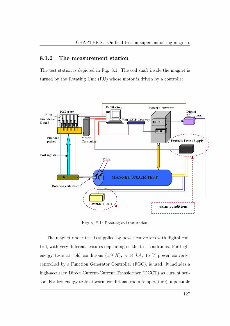
CHAPTER 8. On-field test on superconducting magnets
8.1.2 The measurement station
The test station is depicted in Fig. 8.1. The coil shaft inside the magnet is
turned by the Rotating Unit (RU) whose motor is driven by a controller.
Figure 8.1: Rotating coil test station.
The magnet under test is supplied by power converters with digital con-
trol, with very different features depending on the test conditions. For high-
energy tests at cold conditions (1.9 K), a 14 kA, 15 V power converter
controlled by a Function Generator Controller (FGC), is used. It includes a
high-accuracy Direct Current-Current Transformer (DCCT) as current sen-
sor. For low-energy tests at warm conditions (room temperature), a portable
127
CHAPTER 8. On-field test on superconducting magnets
power supply of 20 A, 135 V is exploited with a portable DCCT as current
sensor. A digital multimeter is used to read the DCCT output signal.
A MRU shaft has 12 segments to cover the length of the magnets. How-
ever, three segments were measured, because a limited number of FDIs were
available (6 FDIs of the pre-series production). Three FDI were used for
the absolute coil signals and three for the compensated ones of three shaft
segments.
The coil signals are integrated in the angular domain by means of the
FDIs, by exploiting the trigger pulses coming out from the encoder board,
suitably processing the output of the encoder mounted on the RU.
The FDI boards, the encoder board, and the motor controller are re-
motely driven by a PC running the test program, developed in the FFMM
environment (see 6.7.1). The static and the dynamic tests are carried out on
the LHC dipoles MBBR2427 and MBA2551, respectively.
8.1.3 The validation procedure
The validation procedure is aimed at verifying that the FDI with the new
software FFMM provide results compatible with the previous PDI-based sys-
tem using the MMP software for the tests of the same LHC dipole, in the
same measurement conditions, exploiting for both the system the TRU shaft.
In the procedure, the field harmonics are evaluated according to the wash-
ing machine algorithm (see 2.1.1), as average of two measurements carried
out by turning the shaft first in one direction (clockwise), and then in the op-
posite one (counter clockwise), in order to cancel any offset and compensate
for possible mechanical plays.
The dipole magnet, supplied by 10 A at a temperature of 152 K, is tested
128
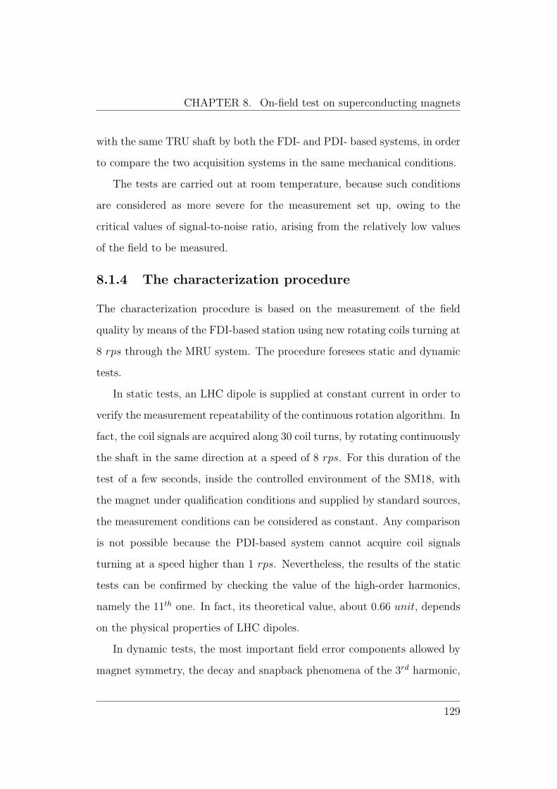
CHAPTER 8. On-field test on superconducting magnets
with the same TRU shaft by both the FDI- and PDI- based systems, in order
to compare the two acquisition systems in the same mechanical conditions.
The tests are carried out at room temperature, because such conditions
are considered as more severe for the measurement set up, owing to the
critical values of signal-to-noise ratio, arising from the relatively low values
of the field to be measured.
8.1.4 The characterization procedure
The characterization procedure is based on the measurement of the field
quality by means of the FDI-based station using new rotating coils turning at
8 rps through the MRU system. The procedure foresees static and dynamic
tests.
In static tests, an LHC dipole is supplied at constant current in order to
verify the measurement repeatability of the continuous rotation algorithm. In
fact, the coil signals are acquired along 30 coil turns, by rotating continuously
the shaft in the same direction at a speed of 8 rps. For this duration of the
test of a few seconds, inside the controlled environment of the SM18, with
the magnet under qualification conditions and supplied by standard sources,
the measurement conditions can be considered as constant. Any comparison
is not possible because the PDI-based system cannot acquire coil signals
turning at a speed higher than 1 rps. Nevertheless, the results of the static
tests can be confirmed by checking the value of the high-order harmonics,
namely the 11th one. In fact, its theoretical value, about 0.66 unit, depends
on the physical properties of LHC dipoles.
In dynamic tests, the most important field error components allowed by
magnet symmetry, the decay and snapback phenomena of the 3rd harmonic,
129
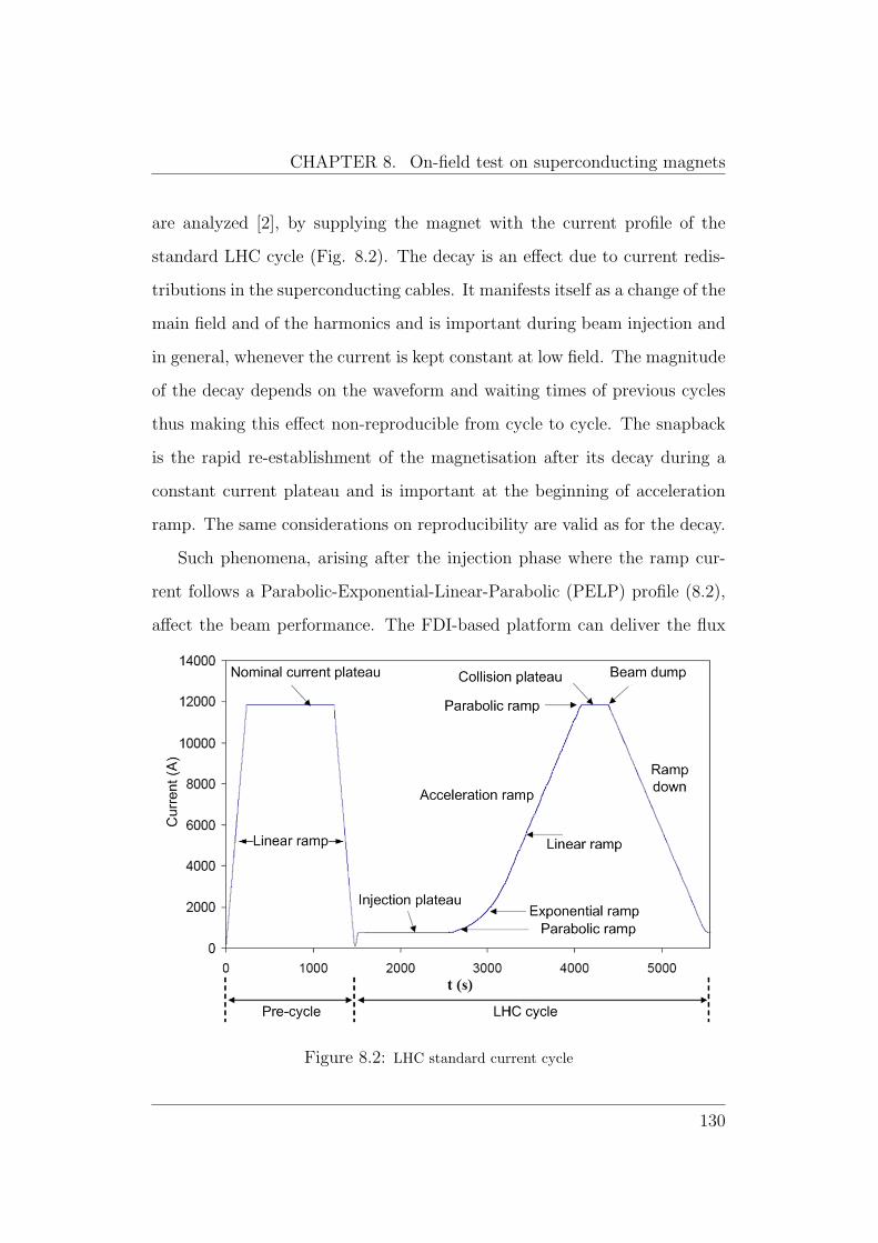
CHAPTER 8. On-field test on superconducting magnets
are analyzed [2], by supplying the magnet with the current profile of the
standard LHC cycle (Fig. 8.2). The decay is an effect due to current redis-
tributions in the superconducting cables. It manifests itself as a change of the
main field and of the harmonics and is important during beam injection and
in general, whenever the current is kept constant at low field. The magnitude
of the decay depends on the waveform and waiting times of previous cycles
thus making this effect non-reproducible from cycle to cycle. The snapback
is the rapid re-establishment of the magnetisation after its decay during a
constant current plateau and is important at the beginning of acceleration
ramp. The same considerations on reproducibility are valid as for the decay.
Such phenomena, arising after the injection phase where the ramp cur-
rent follows a Parabolic-Exponential-Linear-Parabolic (PELP) profile (8.2),
affect the beam performance. The FDI-based platform can deliver the flux
Figure 8.2: LHC standard current cycle
130
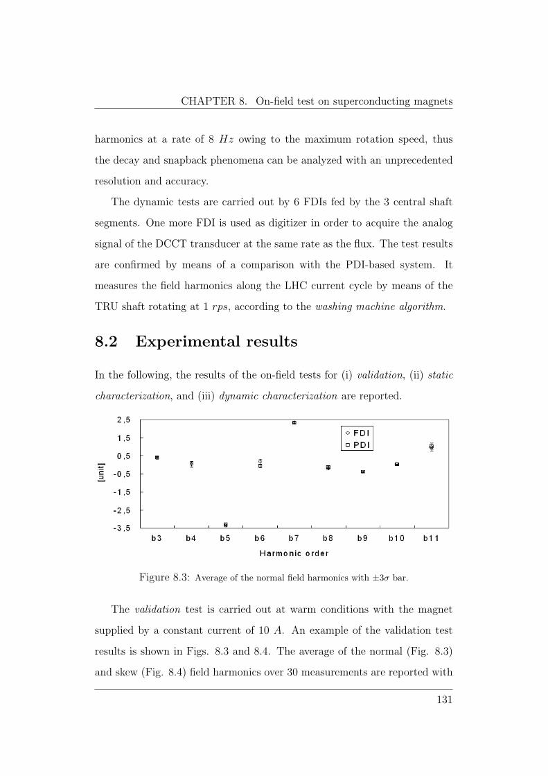
CHAPTER 8. On-field test on superconducting magnets
harmonics at a rate of 8 Hz owing to the maximum rotation speed, thus
the decay and snapback phenomena can be analyzed with an unprecedented
resolution and accuracy.
The dynamic tests are carried out by 6 FDIs fed by the 3 central shaft
segments. One more FDI is used as digitizer in order to acquire the analog
signal of the DCCT transducer at the same rate as the flux. The test results
are confirmed by means of a comparison with the PDI-based system. It
measures the field harmonics along the LHC current cycle by means of the
TRU shaft rotating at 1 rps, according to the washing machine algorithm.
8.2 Experimental results
In the following, the results of the on-field tests for (i) validation, (ii) static
characterization, and (iii) dynamic characterization are reported.
Figure 8.3: Average of the normal field harmonics with ±3σ bar.
The validation test is carried out at warm conditions with the magnet
supplied by a constant current of 10 A. An example of the validation test
results is shown in Figs. 8.3 and 8.4. The average of the normal (Fig. 8.3)
and skew (Fig. 8.4) field harmonics over 30 measurements are reported with
131
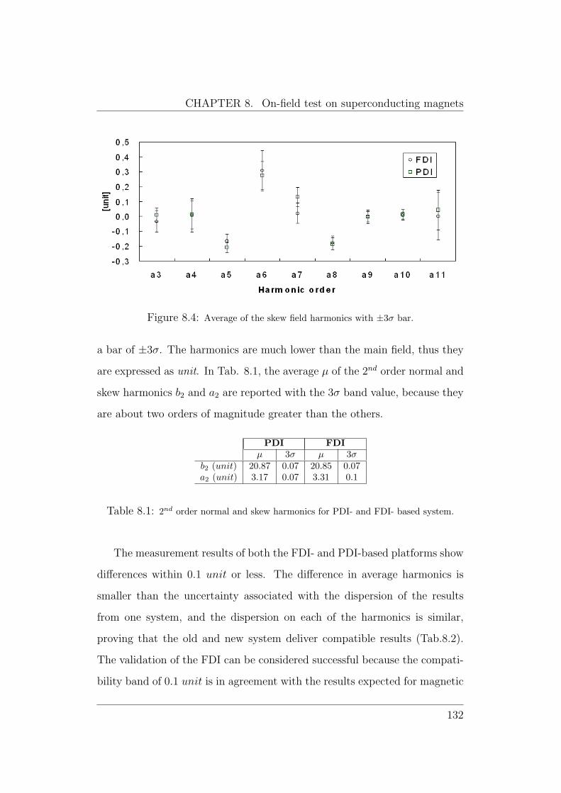
CHAPTER 8. On-field test on superconducting magnets
Figure 8.4: Average of the skew field harmonics with ±3σ bar.
a bar of ±3σ. The harmonics are much lower than the main field, thus they
are expressed as unit. In Tab. 8.1, the average µ of the 2nd order normal and
skew harmonics b2 and a2 are reported with the 3σ band value, because they
are about two orders of magnitude greater than the others.
PDI FDIµ 3σ µ 3σ
b2 (unit) 20.87 0.07 20.85 0.07a2 (unit) 3.17 0.07 3.31 0.1
Table 8.1: 2nd order normal and skew harmonics for PDI- and FDI- based system.
The measurement results of both the FDI- and PDI-based platforms show
differences within 0.1 unit or less. The difference in average harmonics is
smaller than the uncertainty associated with the dispersion of the results
from one system, and the dispersion on each of the harmonics is similar,
proving that the old and new system deliver compatible results (Tab.8.2).
The validation of the FDI can be considered successful because the compati-
bility band of 0.1 unit is in agreement with the results expected for magnetic
132
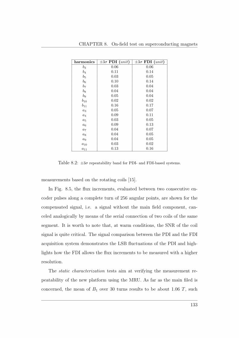
CHAPTER 8. On-field test on superconducting magnets
harmonics ±3σ PDI (unit) ±3σ FDI (unit)b3 0.06 0.06b4 0.11 0.14b5 0.03 0.05b6 0.10 0.14b7 0.03 0.04b8 0.04 0.04b9 0.05 0.04b10 0.02 0.02b11 0.16 0.17a3 0.05 0.07a4 0.09 0.11a5 0.03 0.05a6 0.09 0.13a7 0.04 0.07a8 0.04 0.05a9 0.04 0.05a10 0.03 0.02a11 0.13 0.16
Table 8.2: ±3σ repeatability band for PDI- and FDI-based systems.
measurements based on the rotating coils [15].
In Fig. 8.5, the flux increments, evaluated between two consecutive en-
coder pulses along a complete turn of 256 angular points, are shown for the
compensated signal, i.e. a signal without the main field component, can-
celed analogically by means of the serial connection of two coils of the same
segment. It is worth to note that, at warm conditions, the SNR of the coil
signal is quite critical. The signal comparison between the PDI and the FDI
acquisition system demonstrates the LSB fluctuations of the PDI and high-
lights how the FDI allows the flux increments to be measured with a higher
resolution.
The static characterization tests aim at verifying the measurement re-
peatability of the new platform using the MRU. As far as the main filed is
concerned, the mean of B1 over 30 turns results to be about 1.06 T , such
133
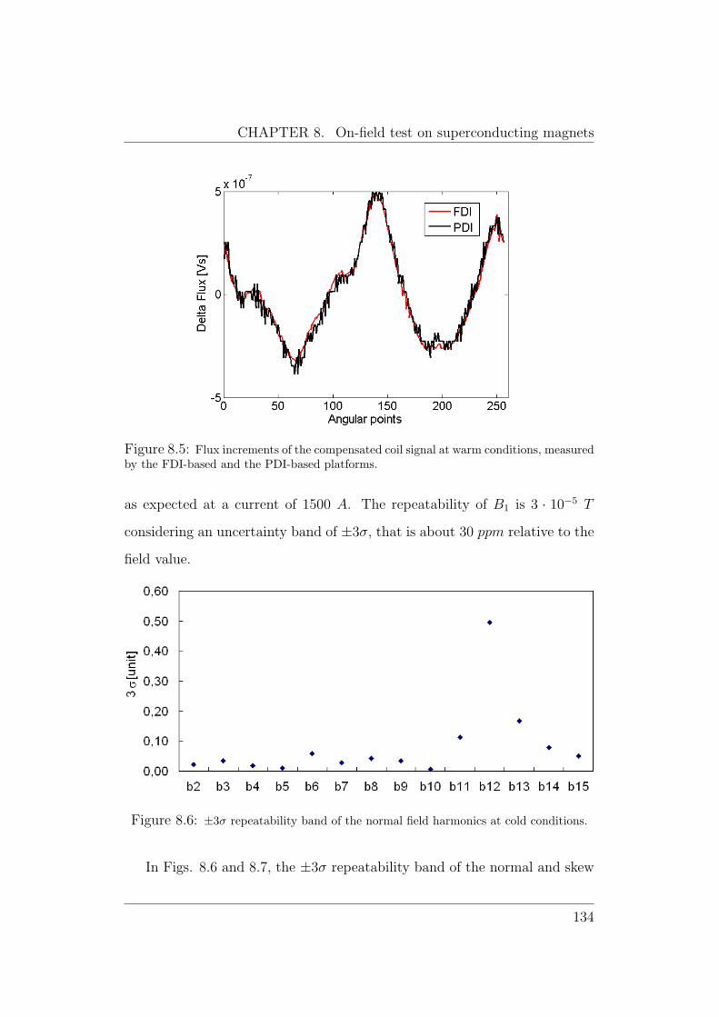
CHAPTER 8. On-field test on superconducting magnets
Figure 8.5: Flux increments of the compensated coil signal at warm conditions, measuredby the FDI-based and the PDI-based platforms.
as expected at a current of 1500 A. The repeatability of B1 is 3 · 10−5 T
considering an uncertainty band of ±3σ, that is about 30 ppm relative to the
field value.
Figure 8.6: ±3σ repeatability band of the normal field harmonics at cold conditions.
In Figs. 8.6 and 8.7, the ±3σ repeatability band of the normal and skew
134
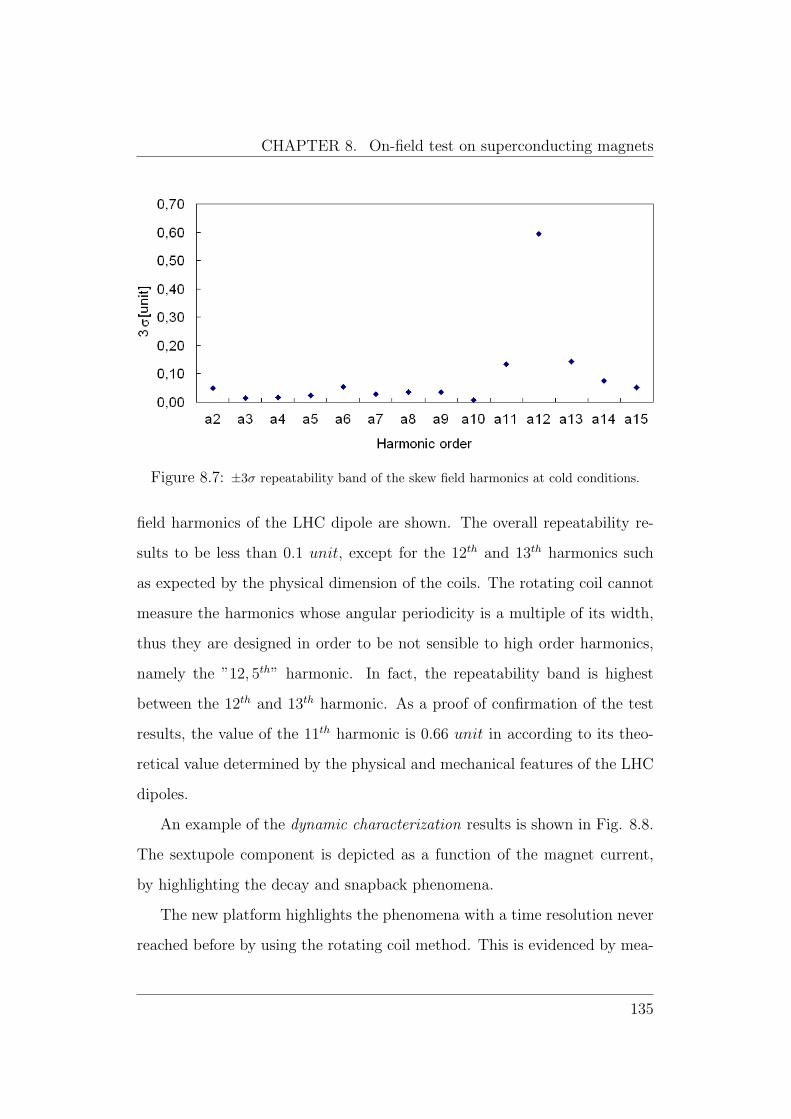
CHAPTER 8. On-field test on superconducting magnets
Figure 8.7: ±3σ repeatability band of the skew field harmonics at cold conditions.
field harmonics of the LHC dipole are shown. The overall repeatability re-
sults to be less than 0.1 unit, except for the 12th and 13th harmonics such
as expected by the physical dimension of the coils. The rotating coil cannot
measure the harmonics whose angular periodicity is a multiple of its width,
thus they are designed in order to be not sensible to high order harmonics,
namely the ”12, 5th” harmonic. In fact, the repeatability band is highest
between the 12th and 13th harmonic. As a proof of confirmation of the test
results, the value of the 11th harmonic is 0.66 unit in according to its theo-
retical value determined by the physical and mechanical features of the LHC
dipoles.
An example of the dynamic characterization results is shown in Fig. 8.8.
The sextupole component is depicted as a function of the magnet current,
by highlighting the decay and snapback phenomena.
The new platform highlights the phenomena with a time resolution never
reached before by using the rotating coil method. This is evidenced by mea-
135
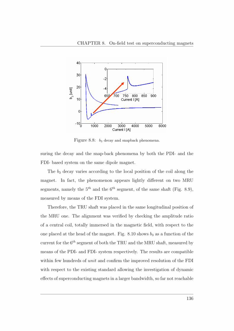
CHAPTER 8. On-field test on superconducting magnets
Figure 8.8: b3 decay and snapback phenomena.
suring the decay and the snap-back phenomena by both the PDI- and the
FDI- based system on the same dipole magnet.
The b3 decay varies according to the local position of the coil along the
magnet. In fact, the phenomenon appears lightly different on two MRU
segments, namely the 5th and the 6th segment, of the same shaft (Fig. 8.9),
measured by means of the FDI system.
Therefore, the TRU shaft was placed in the same longitudinal position of
the MRU one. The alignment was verified by checking the amplitude ratio
of a central coil, totally immersed in the magnetic field, with respect to the
one placed at the head of the magnet. Fig. 8.10 shows b3 as a function of the
current for the 6th segment of both the TRU and the MRU shaft, measured by
means of the PDI- and FDI- system respectively. The results are compatible
within few hundreds of unit and confirm the improved resolution of the FDI
with respect to the existing standard allowing the investigation of dynamic
effects of superconducting magnets in a larger bandwidth, so far not reachable
136
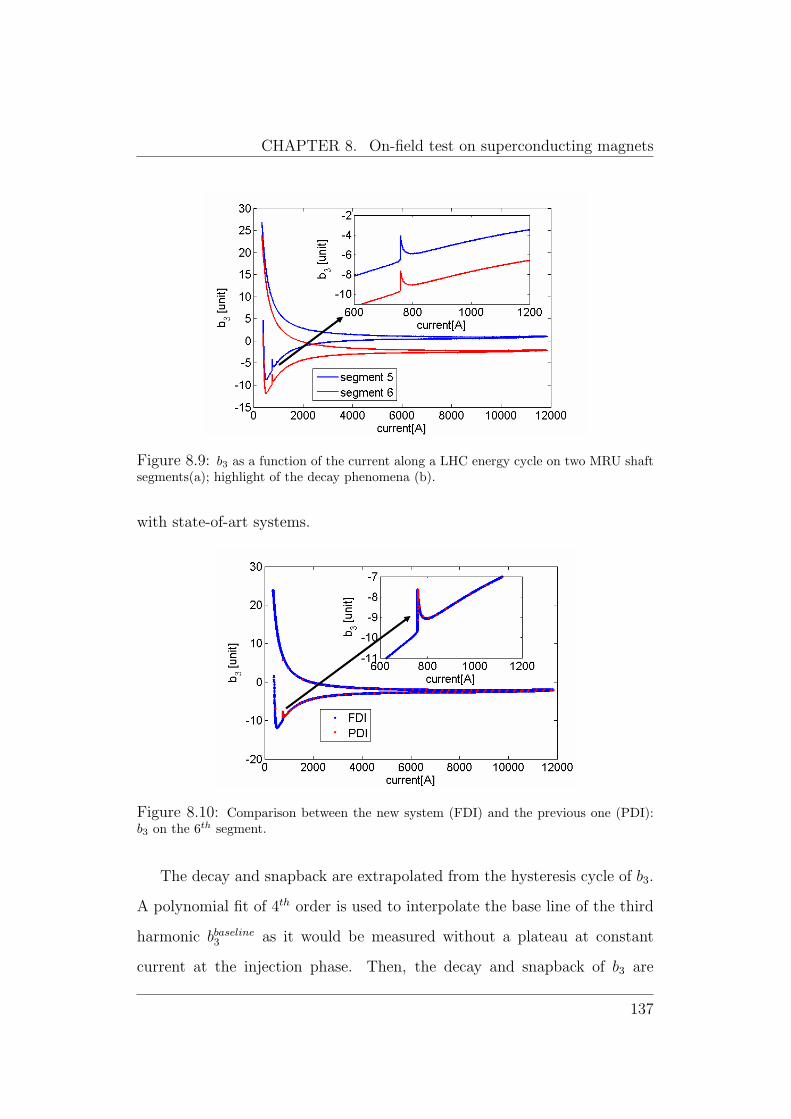
CHAPTER 8. On-field test on superconducting magnets
Figure 8.9: b3 as a function of the current along a LHC energy cycle on two MRU shaftsegments(a); highlight of the decay phenomena (b).
with state-of-art systems.
Figure 8.10: Comparison between the new system (FDI) and the previous one (PDI):b3 on the 6th segment.
The decay and snapback are extrapolated from the hysteresis cycle of b3.
A polynomial fit of 4th order is used to interpolate the base line of the third
harmonic bbaseline3 as it would be measured without a plateau at constant
current at the injection phase. Then, the decay and snapback of b3 are
137
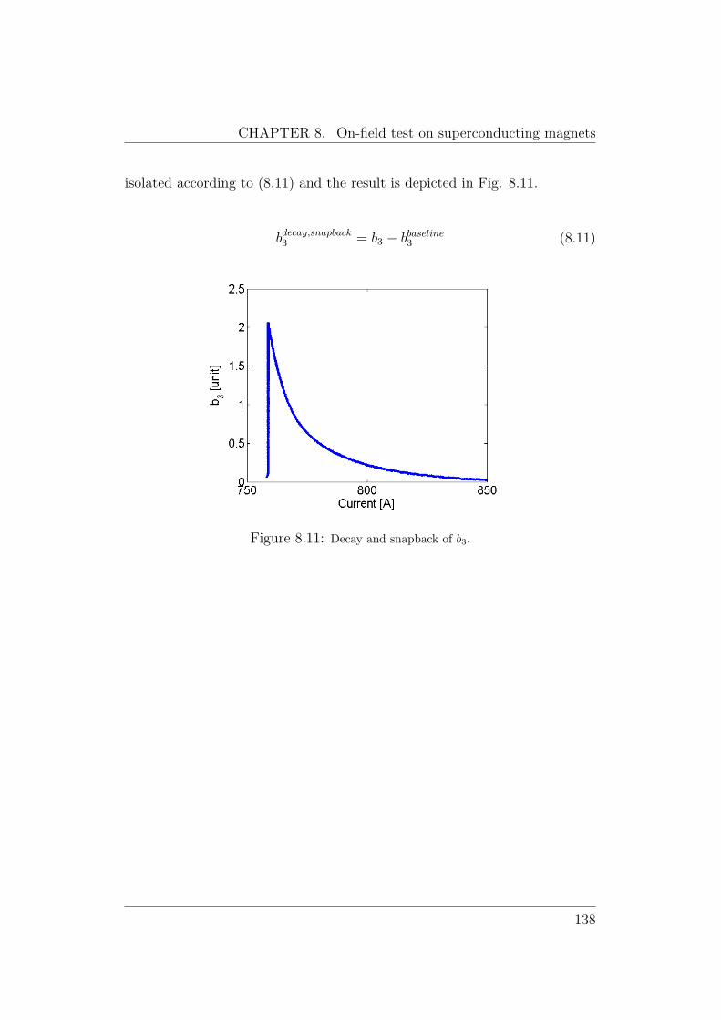
CHAPTER 8. On-field test on superconducting magnets
isolated according to (8.11) and the result is depicted in Fig. 8.11.
bdecay,snapback3 = b3 − bbaseline
3 (8.11)
Figure 8.11: Decay and snapback of b3.
138
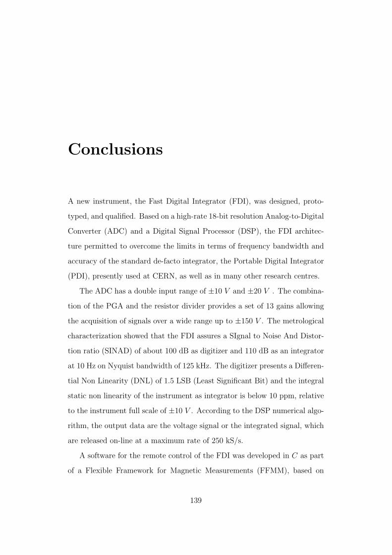
Conclusions
A new instrument, the Fast Digital Integrator (FDI), was designed, proto-
typed, and qualified. Based on a high-rate 18-bit resolution Analog-to-Digital
Converter (ADC) and a Digital Signal Processor (DSP), the FDI architec-
ture permitted to overcome the limits in terms of frequency bandwidth and
accuracy of the standard de-facto integrator, the Portable Digital Integrator
(PDI), presently used at CERN, as well as in many other research centres.
The ADC has a double input range of ±10 V and ±20 V . The combina-
tion of the PGA and the resistor divider provides a set of 13 gains allowing
the acquisition of signals over a wide range up to ±150 V . The metrological
characterization showed that the FDI assures a SIgnal to Noise And Distor-
tion ratio (SINAD) of about 100 dB as digitizer and 110 dB as an integrator
at 10 Hz on Nyquist bandwidth of 125 kHz. The digitizer presents a Differen-
tial Non Linearity (DNL) of 1.5 LSB (Least Significant Bit) and the integral
static non linearity of the instrument as integrator is below 10 ppm, relative
to the instrument full scale of ±10 V . According to the DSP numerical algo-
rithm, the output data are the voltage signal or the integrated signal, which
are released on-line at a maximum rate of 250 kS/s.
A software for the remote control of the FDI was developed in C as part
of a Flexible Framework for Magnetic Measurements (FFMM), based on
139
Object Oriented Programming (OOP) and Aspect-Oriented Programming
(AOP) techniques.
FDI is a part of the project FAst Magnetic Equipment (FAME) aimed at
renewing the park of the magnetic measurement devices at CERN, in order
to analyze more accurately dynamic magnetic fields. The first goal of the
project is the renewal of the rotating coil system, thus a new rotating unit
-the Micro Rotating Unit (MRU)- was designed to turn the coils continuously
up to a speed of 8 rps. On the basis of its performance, the FDI can be used
for magnetic measurements based on the new generation of fast transducers.
The integral field quality can be analyzed in a bandwidth from 1 to 10 Hz,
allowing the accurate analysis of fast magnetic field transients. Therefore,
the first series of the FDI production was integrated in the measurement
station based on the new rotating coils for an on-field test of the new in-
strument. Firstly, the measurement station was validated by comparing the
measurement results with the previous measurement station based on the
PDIs and the Twin Rotating Unit (TRU).
The field harmonics of an LHC dipole were evaluated at warm conditions
and low magnet current, rotating the coils at 1 rps, by using the TRU shaft
for both the PDI- and the FDI- based systems, exploiting the washing ma-
chine algorithm: 3 turns in both the rotation directions are performed in
order to reach a constant speed, acquire a coil turn, and decelerate. The test
showed that the field harmonic values, obtained by means of the PDI- and
the FDI- based systems, are compatible within ±0.1 unit, considering a ±3σ
band.
Then, the FDI prototypes were tested to acquire the coil signals rotated
continuously at 8 rps by the new MRU. The tests were done at cold condi-
140
tions at high magnet current up to 11 kA. The field harmonics were measured
at steady state (constant current) to verify in continuous rotation mode the
repeatability of the station which turns out to be less than ±0.1 unit con-
sidering a ±3σ band. The correctness of the harmonic values was assessed
by verifying the value of high-orders harmonics, namely the 11th harmonic,
whose value is related to the LHC magnet properties.
Furthermore, the new measurement system, made up of the FDIs and the
new rotating coils system, was employed to measure the sextupole component
of a dipole along the LHC current ramp. After the LHC injection phase
at steady state, when the current increases according to the LHC energy
profile, the 3rd harmonic of the magnetic field is affected by the decay and
the snapback, one of the most important dynamic error components of the
LHC magnets since it affects the particle beam features. Such phenomena
were measured at 8 Hz marking an improvement of a factor 100, in terms of
frequency bandwidth with respect to the previous PDI system.
On the basis of these promising results, Metrolab, one of the leader firms
of instrumentation for magnetic measurements, took up the license for pro-
ducing and selling the instrument worldwide.
Other international research centers asked for using the FDI for their
magnet tests. The Berkeley National Laboratory (BNL) wishes to use the
FDI as a computing unit in a feedback loop to control the input current
of small magnets. The GSI Helmholtz Centre for Heavy Ion Research is
interested in testing a new generation of high field, fast-pulsed magnets by
means of the FDI to exploit its large bandwidth. The National Centre of
Oncological Hadrontherapy (CNAO), is looking for a high rate fluxmeter
in order to control the beam trajectory of medical instruments. The FDI
141

could be a valid option by assuring the measurement of the magnetic flux at
minimum period of 4 µs.
The employments of the instrument at CERN as well as in other labo-
ratories will allow the refinement of the instrument by launching the FDI to
become the new standard de-facto integrator for magnetic measurements.
142

Bibliography
[1] ” LHC design report”. CERN - 2004 - 003, 2004.
[2] L. Bottura K. Henrichsen. ”Field measurements”. CERN Accelera-
tor School on Superconductivity and Cryogenics for Accelerators and
Detectors, CERN-2004-008:118–148, 2004.
[3] S. Amet L. Bottura L. Deniau L. Walckiers. ”The multipoles factory:
an element of the LHC control”. IEEE Transactions on Applied Su-
perconductivity, 12:1417–1421, 2002.
[4] W.C. Elmore M.W. Garrett. ”Measurement of two-dimensional fields,
Part I: theory”. Review of Scientific Instrument, 1954.
[5] I.E. Dayton F.C. Shoemaker R.F. Mozley. ”Measurement of two-
dimensional fields, Part II: Study of a quadrupole magnet”. Review
of Scientific Instrument, 1954.
[6] J. DiMarco J. Krzywinski. ”MTF single streched wire system”. Tech-
nical report, Fermi National Accelerator Laberatory, March 1996.
[7] J. DiMarco H. Glass M. J. Lamm P. Schlabach C. Sylvester J. C. Tomp-
kins J. Krzywinski. ”Field alignment of quadrupole magnets for the
LHC interaction regions”. IEEE Transactions on Applied Supercon-
ducitvity, 10(1):127–130, 2000.
143
[8] L. Bottura L. Larsson S. Schloss M. Schneider N. Smirnov. ”A fast
sextupole probe for snapback measurement in the LHC dipoles”. IEEE
Transactions on Applied Superconducitvity, 10(1):1435–1438, 2000.
[9] M. Haverkamp L. Bottura E. Benedico S. Sanfilippo B. ten Haken
H.H.J. ten Kate. ”Field decay and snap-back measurements using a fast
Hall plate detector”. IEEE Transactions on Applied Superconducitvity,
12(1):86–89, 2002.
[10] N.R. Brooks L. Bottura J.G. Perez O. Dunkel. ”Estimation of mechan-
ical vibrations of LHC fast magnetic measurement system”. ”Proceed-
ings of 20th Biennial Conference on Magnetic Technology (MT-20)”,
August 2007. Philadelphia, PE.
[11] A. Jain J. Escallier G. Ganetis W. Louie A. Marone R. Thomas P. Wan-
derer. ”Measurements of the field quality in superconducting dipoles at
high ramp rates”. Proceedings of International Magnetic Measurement
Workshop IMMW14, September 2005. Geneva, Switzerland.
[12] R. Carcagno et Al. ”Superconducting solenoid magnet test results”.
IEEE Transactions on Applied Superconductivity, (2), June 2007.
[13] P. Sievers. ”Towards series measurements of LHC magnets”. CERN
AT/94/11 (MA), 1994. LHC Note 267.
[14] et al. L. Walckiers. ”Towards series measurements of the LHC super-
conducting dipole magnets”. Proceedings of 1997 Particle Accelerator
Conference, pages 3377–3379, 1997.
[15] L. Walckiers L. Bottura M. Buzio P. Schnizer N. Smirnov. ”Sensitivity
and accuracy of the systems for the magnetic measurements of the
144
lhc magnets at CERN”. Proceedings of European Particle Accelerator
Conference, pages 2181–2183, 2000.
[16] A. Masi. ”Advanced measurement systems based on digital processing
techniques for superconducting LHC magnets”. PhD thesis, University
of Naples, FEDERICO II and CERN AT/MTM, Geneva Switzerland,
2005.
[17] J. Billan et al. ”Twin rotating coils for cold magnetic measurements
of 15 m long LHC dipoles”. IEEE Transactions on Applied Supercon-
ducitvity, 10(1):1422–1426, 2000.
[18] P. Galbraith. ”Portable ”Digital ”Integrator”. CERN Internal Tech-
nical note 93-50. AT-MA/PF/fm.
[19] http://www.metrolab.com/uploads/Document.
[20] D.B.Barlow. ”Rotating coil measurements system for the APT/LEDA
CCDTL quadrupole magnets”. IEEE Transactions on Applied Super-
conductivity, 10(1):1447–1449, March 2000.
[21] J.D. Zhang et al. ”Design and fabrication of a rotating coil magnetic
measurement system”. Proceedings of the second Asian Particle Accel-
erator Conference, pages 172–175, 2001. Beijing, China.
[22] W. Pellico P. Colestock. ”Pulsed magnetic field measurement using a
ferrite waveguide in aphase bridge circuit”. Proceedings of the Particle
Accelerator Conference, 3:3716–3718, May 1997.
145
[23] C. Evesque. ”A new challenge in magnet axis transfer”. Proceedings of
International Magnetic Measurement Workshop IMMW11, September
1999. Brookhaven National Laboratory (USA).
[24] R. Carcagno et Al. ”A fast continuous magnetic field measurement
system based on digital signal processor”. Proceedings of 19th Magnet
Technology Conference, September 2005. Genova, Italy.
[25] http://www.home.agilent.com/agilent/product.jspx?nid=-
35501.733416.00 & cc=US & lc=eng.
[26] http://www.eurotech.com/IT/prodotti.aspx?pg=Advme1608A&pc=342.
[27] http://www.entegra.co.uk/c6416 adc dac fpga dsp quixote.htm.
[28] http://www.entegra.co.uk/c6416 pmc fpga dsp quadia.htm.
[29] http://www.ni.com/pxi/.
[30] http://www.dsp-fpga.com/news/db/?6198 .
[31] P. Arpaia L. Bottura A. Masi G. Spiezia. ”Performance analysis of
a fast digital integrator for magnetic field measurements at CERN”.
Measurement Journal, 41:737–743, 2008.
[32] P. Arpaia V. Inglese G. Spiezia S. Tiso. ”Surface-response-based
modeling of digitizers: a case-study on a fast digital integrator at
CERN”. IEEE Transactions on Instrumentation and Measurements,
March 2008. Further coming.
[33] P. Arpaia M. Bernardi L. Bottura M. Buzio L. Deniau G. Di Lucca
V. Inglese G. Spiezia L. Walckiers. ”Kernel design of a flexible soft-
146
ware framework for magnetic measurements at CERN”. IEEE I2MTC
Conference Proceedings, May 2008. Canada.
[34] IEEE std 1057-1994. IEEE Standard for Digitizing Waveform
Recorders, 1994.
[35] P. Arpaia L. Bottura V. Inglese G. Spiezia. ”On-field validation of
the new platform for magnetic measurement at CERN”. Measurement
Journal, April 2008. Further coming.
[36] C. Rubbia. ”Experimental observation of the intermediate vector
bosons w+,w-, and z0”. Almqvist and Wiksell, pages 51–101, 1985.
[37] S. Van der Meer. ” Stochastic cooling and the accumulation of antipro-
tons ”. Almqvist and Wiksell, pages 103–122, 1985.
[38] http://proj-cngs.web.cern.ch/proj-cngs.
[39] S. Mauri. ” The Antiproton Deceleration: AD”. Springer Netherlands,
109:43–52, August 1997.
[40] S. Fartoukh O. Bruning. ”Field quality specification for the LHC main
dipole magnets”. CERN LHC-Project-Report 501, 2001.
[41] R. Schmidt J. Wenninger. ”Machine protection issues and strategies
for the LHC”. Proceedings European Particle Accelerator Conference
EPAC 2004, August 2004. Lucerne, Switzerland.
[42] J. Gareyte. ”Impact of superconductors on LHC design”. CERN 96-03,
pages 335–346, 1996. CERN, Geneva, Switzerland.
147
[43] H. Padamsee. ”Designing superconducting cavities for accelerators”.
CERN 2004-08, pages 233–252, 2004. CERN, Geneva, Switzerland.
[44] L. Rossi. ”Superconducting magnets for the LHC main lattice”. IEEE
Transactions on Applied Superconducitvity, pages 153–158, 2004.
[45] L. Rossi. ”The lhc main dipoles and quadrupoles toward series produc-
tion”. IEEE Transactions on Applied Superconductivity, 13(2):1221–
1228, 2003.
[46] L. Walckiers. ”The harmonic coil method”. CERN Accelerator School
on Magnetic Measurments and Alignment, CERN-92-05:138–166, 1992.
[47] A.K. Jain. ”Harmonic coils”. CERN Accelerator School on Measure-
ment and Alignment of Accelerator and Detector Magnets, CERN-98-
05:175–217, 1998.
[48] R.A. Beth. ”Complex representation and computation of two-
dimensional magnetic fields”. Journal of Applied Physics, 37:2568–
2571, 1966.
[49] S. Bidon J. Billan F. Fischer C. Sanz. ”New technique of fabrication
of search coil for magnetic field measurement by harmonic analysis”.
CERN Internal Note AT-MA 95-117, 1995.
[50] J. Garcıa Perez J. Billan M. Buzio P. Galbraith D. Giloteaux V. Re-
mondino. ”Performance of the room temperature system for magnetic
field measurements of the LHC magnets”. IEEE Transactions on Ap-
plied Superconducitvity, 16(2):269–272, 2006.
148
[51] W. Venturini Delsolaro A. Arn L. Bottura C. Giloux R. Mompo A.
Siemko L. Walckiers. ”The test facility for the short prototypes of the
LHC superconducting magnets”. Proceedings 2001 Cryogenics Engi-
neering Conference, 2001. Madison, Wisconsin, USA.
[52] P. Kusch J.R. Zacharias J.J. Rabi, S. Millman. ”The molecular beam
resonance method for measuring nuclear magnetic moments”. Physical
Review, 55, 1939.
[53] E.M. Purcell H.C. Torrey R.V. Pound. ”Resonance absorption by nu-
clear magnetic moments in a solid”. Physical Review, 69, 1946.
[54] F. Bloch W.W. Hansen M. Packard. ”The nuclear induction experi-
ment”. Physical Review, 70, 1946.
[55] N. Bloembergen E.M. Purcell R.V. Pound. ”Relaxation effects in nu-
clear magnetic resonance absorption”. Physical Review, 73, 1948.
[56] G. zu Putlitz P. von Walter R. Prigl U. Haeberlen K. Jungmann. ”A
high precision magnetometer based on pulsed NMR”. Nuclear Instru-
ments and Methods, A 374, 1996.
[57] N. Kernevez D. Duret M. Moussavi J.-M. Leger. ”Weak field NMR
and ESR spectrometers and magnetometers”. IEEE Transactions on
Magnetics, 28, 1992.
[58] E.H. Hall. ”On a new action of the magnet on electric currents”. Amer-
ican Journal of Mathematics, 2:287–292, 1879.
149
[59] G.L. Pearson. ”A magnetic field strength meter employing the Hall
effect in germanium”. Review of Scientific Instruments, 19:263–265,
1948.
[60] J.M. Kelly. ”Magnetic field measurements with peaking strips”. Review
of Scientific Instrument, 1951.
[61] D.I. Gordon R.E. Brown. ”Recent advances in fluxgate magnetometry”.
IEEE Transactions on Magnetics, pages 76–82, 1972.
[62] F. Primdahl. ”The fluxgate magnetometer”. Journal of Physics E:
Scientific Instruments, pages 241–253, 1979.
[63] F. Primdahl. ”Possible magnetic experiments on the surface of Mars”.
Jourbal of Geophysical Research, pages 1037–1044, 1992.
[64] http://www.pentek.com/products/Detail.cfm?Model=6102.
[65] http://www.pentek.com/products/Detail.cfm?Model=4288.
[66] Y. Kawamata I. Yonekawa K. Kurihara. ”Development of an intelligent
digital integrator for long pulse operation in a Tokamak”. 19th Symp.
On Fusion Engineering, pages 172–175, January 2001.
[67] http://www.GMBH.com.
[68] http://www.vi.rdm-apps.com.
[69] P. Arpaia F. Cennamo P. Daponte H. Schumny. ”Modeling and char-
acterization of Sigma-Delta analog-to-digital converters”. IEEE Trans-
actions on instrumentation and Measurement, 52(3), June 2003.
150
[70] P. Aziz H.V. Sorgensen J. Van Der Spiegel. ”An overview of Sigma-
Delta converters”. IEEE Signal Processing Magazine, pages 61–84,
January 1996.
[71] ”High dynamic range delta-sigma modulator, ads 1201”. Technical
report, Burr-Brown Corporation, March 1999.
[72] ”Dual CMOS Delta-Sigma modulator”. Technical report, Analog De-
vice, 2002.
[73] AD7400 - Isolated Sigma-Delta modulator (10 MHz data rate). Tech-
nical report, Analog Device, January 2006.
[74] G. E. P. Box N. R. Draper. ”Empirical model-building and response
surfaces”. J. Wiley, New York, 1987.
[75] G. E. P. Box W. G. Hunter J. Stuart Hunter. ”Statistics for Exper-
imenters: Design, Innovation, and Discovery”. J. Wiley, New York,
2005.
[76] P. W. A. Lewis. ”Simulation Methodology for Statisticians, Operations
Analysts, and Engineers”. McKenzie, 1988.
[77] L. Ljung. ”State of the art in linear system identification: Time and
frequency domain methods”. Proceedings of 2004 American Control
Conference, July 2004. Boston, MA.
[78] H. Sahai M. I. Ageel. ”Analysis of Variance: Fixed, Random and Mixed
Models”. Birkhauser, Boston, 2000.
[79] B. G. Tabachnick L. S. Fidell. ”Using Multivariate Statistics”. Allyn
and Bacon, New York, 2006.
151
[80] P. Arpaia A. Masi G. Spiezia. ”A digital integrator for fast and accurate
measurement of magnetic flux by rotating coils”. IEEE Transactions
on Instrumentation and Measurements, 56(2), April 2007.
[81] http://www.analog.com/en/analog-to-digital-converters/ad-
converters/ad7674/products/product.html.
[82] P. Arpaia P.Daponte S.Rapuano. ”A state of the art on adc modeling”.
Computer Standards and Interfaces, 26:31–42, 2003.
[83] K. Kim. ”Analog-to-digital conversion and harmonic noises due to
the integral nonlinearity”. IEEE Transactions on Instrumentation and
Measurement, 43(2), April 1994.
[84] http://www.microcrystal.com/productdocuments/variants/OCXOVT.6989.pdf.
[85] D. K. J. Lin. ”Making full use of Taguchi’s orthogonal arrays”. Quality
and Reliability Engineering International, 10:117–121, 1994.
[86] M. H. Kutner C. Nachtsheim J. Neter and W. Li. ”Applied Linear
Statistical Models”. McGraw-Hill-Irwin, New York, 2005.
[87] http://www.analog.com/en/other/militaryaerospace/ad625/products/product.html.
[88] http://www.analog.com/en/analog-to-digital-converters/ad-
converters/AD7634/products/product.html.
[89] http://www.analog.com/en/embedded-processing-dsp/sharc/adsp-
21262/processors/product.html.
[90] http://www.xilinx.com/support/documentation/data sheets/ds099.pdf.
152
[91] D. Giloteaux. Integrateur numerique rapide (FDI): architecture
materielle, logicielle (FPGA) et interface PCI/CPCI. Internal note,
CERN, EDMS 12345671, 2007.
[92] http://www.pxisa.org.
[93] S. Martin. ”Pc-based data acquisition in an industrial environment”.
IEE Colloquium on PC-Based instrumentation, 2:1–3, January 1990.
[94] M.A. Vega-Rodriguez et al. ”Cork stopper classification using FPGAs
digital image processing techniques”. ”EuroMicro Symposium on Dig-
ital Systems Design: Architectures, Methods and Tools”, 2001.
[95] M.V. Popov. ”Pci data acquisition card for application in radia-
tion imaging systems”. IEEE Nuclear Science Symposium Conference,
4:2339–2342, 2004.
[96] H. Muller F. Bal A. David D. Dominguez J. Toledo. ”A flexible card
concept for data acquisition: the PCI-FLIC”. Proceedings of the 12th
IEEE NPSS Real Time Conf, pages 253–259, 2001.
[97] http://www.daqpoint.nl/documents/adlink/PCI-8570,PXI-
8570 Datasheet 6.pdf.
[98] http://www.plxtech.com/products/io/pci9030.asp.
[99] P. Arpaia V. Inglese G. Spiezia. ”Metrological characterization of an
improved DSP-based on-line integrator for magnetic measurements at
CERN”. Proceedings of IEEE IMTC 2007, May 2007. Warsaw.
[100] J. Bosch. ”Design of an Object-Oriented Framework for Measurement
Systems”. John Wiley, 1999.
153
[101] L. Madaro A. Rijllard R. Saban L. Walckiers L. Bottura P. Legrand. ”A
VME-based LabVIEW system for the magnetic measurements of the
LHC prototype dipoles”. Proceedings of European Particle Accelerator
Conference, 1996. Spain.
[102] A. Guerrero J-J Gras J-L Nougaret M. Ludwig M. Arruat S. Jack-
son. ”Cern front-end software architecture for accelerator controls”.
Proceedings of International Conference on Accelerator and Large Ex-
perimental Physics Control Systems, 2003. Gyeongiu, Korea.
[103] J. M. Nogiec J. Di Marco S. Kotelnikov K. Trombly-Freytag D. Wal-
bridge M. Tartaglia. ”Configurable component-based software system
for magnetic field measurements”. IEEE Transactions on Applied Su-
perconductivity, 16(2):1382–1385, June 1996.
[104] http://www.tango-controls.org.
[105] M. Kersten J. Palm W. G. Griswold G. Kiczales E. Hilsdale J. Hugunin.
”An overview of AspectJ”. Proceedings of 15th European Conference
on Object-Oriented Programming 2001, 2001. Budapest, Hungary.
[106] P. Arpaia L. Bottura M. Buzio D. Della Ratta L. Deniau V. Inglese
G. Spiezia S. Tiso L. Walckiers. ”A software framework for flexible
magnetic measurements at CERN”. Proceedings of IEEE IMTC, May
2007. Warsaw.
[107] P. Arpaia M. Bernardi G. Di Lucca V. Inglese G. Spiezia. ”Fault self-
detection of automatic testing systems by means of aspect-oriented
programming”. Proceedings of 15th IMEKO TC4 Symposium, 2007.
Iasi, Romania.
154
[108] P. Arpaia M. Bernardi G. Di Lucca V. Inglese G. Spiezia. ”An aspect
oriented-based software architectural framework for synchronization in
measurement systems”. Proceedings of 16th IMEKO TC4 Symposium,
September 2008. Florence, Italy.
[109] P. Arpaia L. Bottura V. Inglese G. Spiezia. ”A flexible framework for
magnetic measurements at CERN: a prototype for the new generation
rotating coils”. Proceedings of 15th IMEKO TC4 Symposium, 2007.
Iasi, Romania.
[110] PXI System Alliance. ”PXI hardware specification”. Revision 2.2,
September 2002.
[111] ISO ENV 13005. ”Guide to the expression of uncertainty in measure-
ment”. Geneva, 1995.
[112] A. H. Nuttall. ”Time windows with very good sidelobe behavior”.
IEEE Transactions on Acustic Speech and Signal Processing, ASSP-
29(1), 1981.
[113] T. Shanley D. Anderson. ”PCI System Architecture”. Addison-Wesley,
1995.
[114] P. Arpaia G. Spiezia. ”Performance analysis of the pxi-based bus com-
munication of a fast digital integrator for magnetic measurements”.
Proceedings of 16th IMEKO TC4 Symposium, September 2008. Flo-
rence, Italy.
[115] A. David. ”Performance issues in pci reading”.
http://adavid.home.cern.ch/adavid/public/NA60/online/PCIReadingNote,
2001.
155

[116] M. Floris D. Marras G. Usai A. David P. Rosinsky H. Ohnishi. ”The
NA60 experiment readout architecture”. IEEE Transactions On Nu-
clear Science, 51(3), 2004.
[117] P. Costi-Kowolik R. Gutierrez-Mazon. ”A first approach towards
a high-speed PCI-based data acquisition card for industrial applica-
tions”. IEEE 24th Convention of Electrical and Electronics Engineers,
2006. Israel.
[118] http://sm18-operation.web.cern.ch/sm18-
operation/DefaultIntranet.asp?wycf=0.
[119] L. Bottura. ”Standard analysis procedures for field quality measure-
ment of the LHC magnets. Part i: Harmonics”. LHC Engineering
specification, EDMS 313621.
156


