Probing light-matter interactions in atomically thin 2D material
By
Jonghwan Kim
A dissertation submitted in partial satisfaction of the
requirements for the degree of
Doctor of Philosophy
in
Physics
in the
Graduate Division
of the
University of California, Berkeley
Committee in charge:
Professor Feng Wang, Chair
Professor Michael F. Crommie
Professor Xiang Zhang
Spring 2015


1
Abstract
Understanding light-matter interactions in atomically thin 2D material
by
Jonghwan Kim
Doctor of Philosophy in Physics
University of California, Berkeley
Professor Feng Wang, Chair
Recently, atomically thin 2D materials have emerged as a new class of nanomaterial with
extraordinary physical properties ranging from semi-metal (graphene), semiconductors (transition
metal dichalcogenides) to insulators (hBN). Due to its unusual linear electronic spectrum,
graphene has been studied as a platform where exotic quantum mechanical phenomena take place
and electro-optical property can be greatly tuned by electrostatic gating. On the other hand, in
semiconducting transition metal dichalcogenides (TMD), many body particles such as exciton and
trion can be readily accessed even at room temperature due to strong Coulomb interaction. There
are further exciting opportunities in heterostructures where layer-layer interaction provides new
physics and functionalities. In this thesis, I explore light-matter interaction in 2D materials and
their heterostructure with laser spectroscopy techniques.
First of all, I study electromagnetic interaction between graphene and optical cavity via Rayleigh
scattering spectroscopy. Although light-matter interaction in graphene is extremely strong for
atomically thin thickness, overall optical response in macroscopic scale is still limited.
Combination of graphene and resonant cavity can amplify the interaction dramatically. Therefore,
it is important to understand the electromagnetic interaction between two systems. In this study, I
find that the coupling can be explained by real and imaginary part of graphene dielectric constant
which affects cavity resonance frequency and quality factor, respectively. In addition to

2
fundamental interest, it also shows that this platform has promising potential for novel sensing
application and electro-optical modulator.
Secondly, I study valley-selective dipole interaction of exciton states in a monolayer transition
metal dichalcogenides. Due to crystal symmetry, an extra degree of freedom, valley state, is
available in this system. In analogy to spin state, it is important to understand and manipulate
valley state with light. In this study, I demonstrate that valley excitonic states in a monolayer WSe2
can be manipulated by femtosecond pulse with the control of polarization. Ultrafast pump-probe
spectroscopy shows that circularly-polarized femtosecond pulse induces valley-selective optical
Stark effect which acts as a pseudomagnetic field. This demonstrates efficient and ultrafast control
of the valley excitons with optical light, and opens up the possibility to coherent manipulate the
valley polarization for quantum information applications.
Lastly, I study interlayer interaction in heterostructure of MoS2/WS2 where strong exciton binding
energy plays an important role. Simple band theory predicts that a heterostructure of two different
semiconducting TMD layers forms type-II heterostructure. However, it is not clear how strong
Coulomb interaction plays a role in terms of charge transfer dynamics. In this study, I demonstrate
ultrafast charge transfer in MoS2/WS2 via both photoluminescence mapping and femtosecond (fs)
pump-probe spectroscopy. Despite large exciton binding energy, hole transfer from the MoS2 layer
to the WS2 layer takes place within 50 fs after optical excitation. Such ultrafast charge transfer in
van der Waals heterostructures indicates that it can enable novel 2D devices for optoelectronics
and light harvesting.
i
Contents
LIST OF FIGURES……………………………………………………………... iii
ACKNOWLEDGEMENTS…………………………………………………….. iv
CHAPTER 1 – INTRODUCTION…………………………………………….. 1
1.1 MOTIVATION AND BACKGROUND…………………………… 1 1.2 GRAPHENE………………………………………………………… 2
1.2.1 Electronic band structure…………………………………... 2 1.2.2 Optical property…………………………………………….. 3
1.3 A MONOLAYER MX2…………………………………………….. 5 1.3.1 Electronic band structure………………………………….. 5 1.3.2 Strong coulomb interaction………………………………... 6 1.3.3 Valley degree of freedom…………………………………... 7
1.4 THESIS HIGHLIGHTS …………………………………………… 8
CHAPTER 2 – ELECTRICAL CONTROL OF OPTICAL PLASMON RESONANCE WITH GRAPHENE MOTIVATION AND BACKGROUND
2.1 INTRODUCTION………………………………………………….. 10 2.1.1 Tunable interband transition in graphene………………... 11
2.2 EXPERIMENT……………………………………………………... 13 2.2.1 Optical spectrum measurement……………………………. 13 2.2.2 Sample preparation………………………………………… 13
2.3 RESULT AND DISCUSSION……………………………………… 15 2.3.1 Effect of graphene…………………………………………… 15 2.3.2 Cavity modulation with electrostatic gating………………. 16 2.3.3 Numerical simulation and possibility
as a bio/chemical sensing……………………………………. 20 2.4 COMPARISON TO HYBRID STRUCTURE WITH PHOTONIC
CRYSTAL CAVITY………………………………………………… 21 2.4.1 Photonic crystal cavity………………………………………. 22 2.4.2 Effect of graphene on high Q cavity………………………... 23 2.4.3 Possibility as a fast electro-optic modulator……………….. 23
2.5 CONCLUSION………………………………………………………. 25
CHAPTER 3 – ULTRAFAST GENERATION OF PSEUDOMAGNETIC FIELD FOR VALLEY EXCITONS IN WSE2 MONOLAYERS……………………... 26
3.1 INTRODUCTION…………………………………………………… 26 3.1.1. Optical Stark effect………………………………………….. 27

ii
3.1.2. Valley-selective dipole interaction in MX2…………………. 28 3.2 EXPERIMENT………………………………………………………. 29
3.2.1 Photoluminescence and linear absorption measurement…. 29 3.2.2 Transient absorption spectrum measurement (Pump-probe
spectroscopy)…………………………………………………. 29 3.2.3 CVD-grown monolayer WSe2 sample……………………… 30
3.3 RESULT AND DISCUSSION………………………………………. 31 3.3.1 Optical transition in a monolayer WSe2…………………… 31 3.3.2 Circular polarization dependent photoluminescence……… 32 3.3.3 Valley-selective optical Stark effect…………………………. 33 3.3.4 Control of energy shift with pump power and detuning…... 37 3.3.5 Estimation of pseudomagnetic field magnitude……………. 38
3.4 CONCLUSION AND OUTLOOK………………………………….. 39
CHAPTER 4 – ULTRAFAST CHARGE TRANSFER IN MOS2/WS2 HETEROSTRUCTURE…………………………………………………………. 40
4.1 INTRODUCTION……………………………………………………. 40 4.2 EXPERIMENT……………………………………………………….. 42
4.2.1 Photoluminescence and Raman spectroscopy……………… 43 4.2.2 (Transient) Absorption spectroscopy……………………….. 43 4.2.3 Heterostructure preparation………………………………… 43
4.3 RESULT AND DISCUSSION………………………………………. 43 4.3.1 Optical micrograph of sample and Raman spectra……….. 43 4.3.2 Photoluminescence spectrum and
mapping of heterostructure………………………………… 44 4.3.3 Transient absorption measurement………………………... 46 4.3.4 Determination of charge transfer time…………………….. 49 4.3.5 Effect of Coulomb interaction and lattice mismatch on charge
transfer dynamics……………………………………………. 51 4.4 CONCLUSIONS AND OUTLOOK………………………………… 52
BIBLIOGRAPHY….……………………………………………………………... 54

iii
List of Figures
Figure 1.1 Lattice structure of graphene………………………………………………………………… 2
Figure 1.2 Band structure of graphene by tight binding model………………………………………… 3
Figure 1.3 Illustration of tunable interband transition in graphene…………………………………… 4
Figure 1.4 Lattice structure of a monolayer MX2………………………………………………………. 5
Figure 1.5 Band structure of a monolayer MX2 near K and K’ points………………………………... 6 Figure 2.1 Gate-dependent complex dielectric constant of graphene………………………………….. 13
Figure 2.2 SEM image of a gold nanorod………………………………………………………………… 14
Figure 2.3 Effect of graphene on the gold nanorod plasmon resonance……………………………….. 16
Figure 2.4 Electrical control of the plasmon resonance…………………………………………………. 18
Figure 2.5 Comparison between experiment and theory………………………………………………… 19
Figure 2.6 Numerical simulation result…………………………………………………………………… 21
Figure 2.7 Scanning electron micrograph (SEM) of the fabricated cavities with graphene…………… 22
Figure 2.8 Effect of graphene on high Q cavity…………………………………………………………… 23
Figure 3.1 Illustration of optical Stark effect……………………………………………………………… 28
Figure 3.2 Optical micrograph of a monolayer WSe2 on sapphire substrate…………………………… 31
Figure 3.3 Absorption spectra of a monolayer WSe2…………………………………………………….. 32
Figure 3.4 Circular polarization dependent photoluminescence spectra………………………………... 33
Figure 3.5 Valley-dependent optical Stark effect with non-resonant circularly polarized pump…….... 34
Figure 3.6 Time evolution and spectral lineshape of the valley-dependent transient reflection spectra for pump and probe configuration…………………………………………………………………………. 36
Figure 3.7 Pump detuning and pump intensity dependence of the valley-selective optical Stark shift… 38
Figure 4.1 Band alignment and structure of MoS2/WS2 heterostructures……………………………….. 41
Figure 4.2 Schematic of heterostructure and Raman spectra…………………………………………….. 44
Figure 4.3 Photoluminescence (PL) spectra and mapping of MoS2/WS2 heterostructures at 77 K……. 45
Figure 4.4 Transient absorption spectra of MoS2/WS2 heterostructures………………………………… 48
Figure 4.5 Ultrafast hole transfer dynamics from vertical cuts in Figure 4.4a and 4.4b……………....... 50

iv
Acknowledgment
It is difficult to find words to sufficiently express my gratitude to my advisor, Prof. Feng Wang. I
was extremely lucky to meet him during the exchange program 8 years ago. I dreamed to become
a physicist after I observed high standard and exciting research in his group as an undergraduate
intern. During PhD program under his guidance, I could obtain numerous valuable academic assets
for my future career such as presentation skill with clarity and critical reasoning with good
understanding on physics.
I am also grateful to Prof. Yuen-Ron Shen. In addition to his endless enthusiasm and extraordinary
excellence in physics, I observed a pathway to great science from his successful students and post-
docs.
I could not ask for better colleagues than the students and postdoctoral fellows in Wang group.
Not only being good physicists, they are also great as human being which made me enjoy 5 years
as a graduate student. Dr. David J. Cho, Dr. Steven Byrnes and Dr. Tsung-Ta Tang helped to get
my own research started in my first year. Also, as senior fellows with tough duties, they taught me
how to become a responsible lab member. Dr. Arka Majumdar showed me different aspects of
research from engineering side. While working and having a discussion with him, I started to think
about what is an important and interesting problem to myself instead of chasing what other people
like. I am truly indebted to Dr. Xiaoping Hong for many things. He thought me various skills in
ultrafast optics and software to perform desired experiment in the most accurate and efficient ways.
Working with him, I observed great successes thanks to his optimism and persistence which shaped
my attitude to scientific research. Without him, it is hard to imagine how I could grow up as who

v
I am now. Dr. Sufei Shi showed how to communicate with people outside the group in the
professional manner. He generously gave an advice for academic career which help to plan my
own. Also, his expertise in electrical transport was invaluable for my projects. I was very lucky to
meet Chenhao Jin. He is probably one of the smartest I have ever met among my ages. He is not
only brilliant in fundamental physics but also obtains experimental data with high standard. I
especially appreciate for his theoretical support on projects. I would like to thank Steve Drapcho
for his help on developing techniques for 2D heterostructures. The technique enabled many
interesting projects. My thanks also goes to other members, past and present, Long Ju, Jason Horng,
Bo Zeng, Halleh B. Balch, Yaqing Bie, Dr. Zhiwen Shi, Dr. Jihun Kang, Lili Jiang, Dr. Huiling
Han, Dr. Yinghui Sun, Dr. Yu-Chieh Wen, Dr. Kaihui Liu, Dr. Baisong Geng, Hyungmok Son,
Jingying Yue and Matthew Kam.
I am also grateful to colleagues outside Wang group. Prof. Junqiao Wu, Dr. Sefaattin Tongay,
Joonki Suh provided high quality crystals and nano fabrication. Prof. Yanfeng Zhang and Yu
Zhang provided CVD-grown MoS2 and WS2 samples. Prof. Lance Li, Chih-Yuan S. Chang, and
Ming-Hui Chiu provided CVD-grown WSe2 samples. Also, I would like to thank Prof. Mike
Crommie and Prof. Xiang Zhang for their advice and encouragement as thesis co-advisers.
Finally and most importantly, I want to thank my parents and my sister for their love, care and
belief in me for the past thirty years. My father himself taught me science and mathematics when
I was young which made me begin to enjoy science. My mother supported me both emotionally
and physically. I rely on my sister many things for my family while I am far apart from Korea.
Without them, my life would never be pleasant and fulfilling. This thesis is dedicated to them.

1
Chapter 1. Introduction
1.1 Motivation and background
An atomically thin two-dimensional structure had known to be thermodynamically
unstable so that it cannot exist in nature. It has been only a decade when free-standing 2D materials
are isolated from layered materials. Layered materials has strong in-plane covalent bonding
whereas it has weak out-of-plane van-der-Waals bonding. Thus, they can be cleaved layer by layer.
Geim and Novoselov discovered that these materials can be actually thinned down to a monolayer
by micromechanical exfoliation method. They demonstrated that a monolayer of graphite, MoS2
and other layered materials can be obtained in the laboratory[1].
Isolation of such monolayers was big enough surprise, but shortly people discovered
exciting new possibilities of these new materials in terms of fundamental physics and novel device
applications. Different layered materials have distinct electronic properties such as a
superconductor, metal, semi-metal, semiconductor and insulator. It is unexplored and interesting
questions how two dimensionality affect such electronic properties. Furthermore, there is even
bigger opportunities by combining different monolayers to form a heterostructure[2].
My research focuses on understanding optical properties of such atomically thin 2D
materials and heterostructures for novel optoelectronics applications. In this chapter, I will
introduce electronic band structure and optical properties of 2D materials, graphene and a
monolayer MX2, which are of main focus in my study.

2
1.2 Graphene
1.2.1 Electronic band structure
Graphene is a two-dimensional single atomic layer of carbon atoms. It has a hexagonal
lattice structure with two equivalent carbon atoms as sublattice. It forms like a Honeycomb
structure as shown in Figure 1.1. Carbon atoms form SP2 bonding. Important electrical and optical
properties arise from extra pz orbitals of a carbon atom. Electronic band structure can be calculated
by tight binding model with the nearest neighbor couplings of this pz orbital[3].
Figure 1.1 Lattice structure of graphene Dashed box denotes sublattice sites A and B where two identical carbon
atoms locate.
Band structure shows that conduction and valence bands are meeting at two single points,
so called Dirac point, at K and K’ point. At Dirac point, it possesses a conical electronic structure
where band dispersion is linear. Due to such a unique linear dispersion, a low-energy electron in
graphene behaves like a massless particle and thus its motion should be described by Dirac

3
equation rather than Schrodinger equation[1]. For this reason, graphene is a tabletop platform
where theory for quantum electrodynamics can be tested. As a result, it has attracted an enormous
interest and effort to understand its fundamental behavior of charge carrier in graphene.
Figure 1.2 Band structure of graphene by tight binding model Conduction band and valence band meet at single
points at K and K’ points in momentum space. Band dispersion is linear near Dirac points.
1.2.2 Optical property
Besides fascinating electrical properties, graphene has unique and interesting optical
properties. Despite its single atomic thickness, light-matter interaction in graphene is extremely
strong. Pristine graphene absorbs light at optical frequency by 2.3 percent which is twenty times
stronger than absorption coefficient of GaAs at band edge for the same thickness[4]. Furthermore,
absorption covers broad spectrum ranging from the far infrared to the ultraviolet. What is even
more interesting is that strong and broadband optical response can be tuned by electrostatic doping.
Light absorption in graphene originates from two different contributions: intraband
transition and interband transition. Depending on the spectral frequency, one optical transition is

4
relatively more important than the other. At optical frequency, interband transition play a dominant
role than intraband transition from free carrier[5]. Absorption spectrum of pristine graphene due
to interband transition is frequency independent, and it is determined by the fine-structure constant,
πα. Interband transition in graphene can be modified dramatically with electrostatic doping. This
is because density of state near Dirac point is small so that Fermi level can be tuned by significant
energy difference. As a result, optical transition can be turned on and off by Pauli blocking (Figure
1.3)[4]. In chapter 5, more detailed will be discussed.
Figure 1.3 Illustration of tunable interband transition in graphene A and B show band structure of graphene
where Fermi level is tuned by electrostatic doping. Compared to pristine graphene (A) where Fermi level locates at
Dirac point, highly doped graphene (B) has significantly lowered (hole doping) or raised (electron doping) Fermi level.
As a result, optical transition (blue arrow) can be blocked due to Pauli blocking.
1.3 A monolayer MX2
1.3.1 Electronic band structure

5
Figure 1.4 Lattice structure of a monolayer MX2 A. (Top view) Magenta atom corresponds to transition metal
atom and yellow atom corresponds to chalcogen atom. B. (Side view) Three layered structure of unit layer MX2.
A monolayer MX2 also has a honeycomb lattice structure. In this system, d-electron
orbitals plays important roles[6, 7]. In comparison to graphene, main difference of interest is
broken inversion symmetry in sublattice sites. Site ‘A’ has a transition metal atom (Mo and W),
and site ‘B’ has two chalcogen atoms (S and Se) as shown in Figure 1.4. Different combination of
transition metal atom and chalcogen atom show qualitatively similar behavior. Such explicitly
broken inversion symmetry makes electronic structure of monolayer MX2 distinct from graphene.

6
Figure 1.5 Band structure of a monolayer MX2 near K and K’ points Green and red arrows represent a spin state
of bands.
Figure 1.5 shows electronic band structure of a monolayer MX2[8]. First of all, instead of
a pair of Dirac cone with zero band gap, it has a pair of degenerate direct band gap at K and K’
point. Zero band gap in graphene originates from inversion symmetry in two sublattice sites. In
this sense, finite band gap in a monolayer MX2 can be understood by the broken symmetry.
Especially, band gap locates at visible frequency which makes this system favorable to various
optoelectronic applications. In addition, broken inversion symmetry provides other unique
advantages for spintronics and valleytronics in this system. I will discuss on this shortly below.
1.3.2 Strong coulomb interaction
Although band theory with symmetry consideration can predicts an electronic band
structure, a simple one particle theory is not enough to describe real optical properties of this
system. One needs to consider strong Coulomb interaction among charge carriers[9-11]. Especially,
such effect becomes dramatic in low dimensional system as screening of electric field between
quasiparticles is suppressed significantly. As a result, exciton in a monolayer MX2 has large

7
binding energy according to 2D hydrogenic model (eq. 1.1). Experimentally, such large binding
energy (> 0.5 eV) is confirmed by different techniques such as reflection contrast measurement,
two-photon absorption measurement and scanning tunneling microscopy. Large exciton binding
energy in this system is an important issue to understand physical properties in a heterostructure
which will be discussed in Chapter 4.
/ (eq. 1.1)
: , : , :
1.3.3 Valley degree of freedom
In general, a valley state refers to degenerate local electronic band structure in momentum
space arising from crystal symmetry. Well-known example is Si which as diamond-like lattice
structure. It has multiple degenerate points in momentum space, and they can be controlled by
strain. However, valley state in Si is difficult to control[12]. On the other hand, a monolayer MX2
have valley states at their band gap and it is relatively easier to control[8]. From hexagonal lattice
symmetry, it has two degenerate direct bandgap at K and K’ point in momentum space. Due to
explicitly broken inversion symmetry, spin states split its degeneracy and couple to so-called
valley states. Although inversion symmetry is broken, time reversal symmetry is not broken. With
such condition, eq. 1.2 shows that a spin state at two different valleys cannot have the same energy.
Together with strong spin-orbit coupling from a transition metal atom, spin states at each valley
splits with large energy in an opposite way as shown in Figure 1.5. This is particularly useful for
potential spintronics/valleytronics applications as spin and valley relaxation time can be potentially
slow. This is because flipping spin index alone is forbidden by the valley-contrasting spin splitting.
Time reversal symmetry: ↑ ↓ (eq. 1.2)

8
Broken inversion symmetry: ↑ ↑
Third, optical selection rules at two valleys depends on circular polarization of incident
light. This is because of valley-contrasting dipole interaction matrix element against circular
polarization excitation. I will discuss on this more detailed in Chapter 3. Valley selective dipole
interaction provides powerful control for valley and spin states in this system.
1.4 Thesis highlights
In the following chapters, I will show my work on understanding optical properties of
graphene and a monolayer MX2.
In Chapter 2, I demonstrate that optical resonances in a gold nanorod and photonic crystal
cavity can be efficiently modulated by graphene where Fermi level is tuned by electrostatic doping.
Exploiting the uniquely strong[13, 14] and gate-tunable interband transitions[4, 15] of graphene, I
could achieve significant modulation of both the resonance frequency and quality factor of the
resonantor. For a god nanorod case, our analysis shows that the plasmon-graphene coupling is
remarkably strong: even a single electron in graphene at the plasmonic hotspot could have an
observable effect on plasmon scattering intensity. Such hybrid graphene-nanometallic structure
provides a powerful way for electrical control of plasmon resonances at optical frequencies, and
could enable novel plasmonic sensing down to single charge transfer events. On the other hand, a
graphene-photonic crystal device can potentially be useful for a high speed, and low power
absorptive and refractive modulator, while maintaining a small physical footprint.
9
In Chapter 3, I demonstrate that an ultrafast and ultrahigh valley pseudo-magnetic field can
be generated using circularly polarized femtosecond pulses to selectively control the valley degree
of freedom in monolayer MX2. Employing ultrafast pump-probe spectroscopy, I observed a pure
and valley-selective optical Stark effect in WSe2 monolayers from the non-resonant pump, which
instantaneously lift the degeneracy of valley exciton transitions without any dissipation. The
strength of the optical Stark effect scales linearly with both the pump intensity and the inverse of
pump detuning. An energy splitting more than 10 meV between the K and K’ valley transitions
can be achieved, which corresponds to an effective pseudo-magnetic field over 60 Tesla. This
study demonstrates efficient and ultrafast control of the valley excitons with optical light, and
opens up the possibility to coherent manipulate the valley polarization for quantum information
applications.
In Chapter 4, I show the experimental observation of ultrafast charge transfer in photo-
excited MoS2/WS2 heterostructures using both photoluminescence mapping and femtosecond (fs)
pump-probe spectroscopy. I find that hole transfer from the MoS2 layer to the WS2 layer takes
place within 50 fs after optical excitation, a remarkable rate for van der Waals coupled 2D layers.
Such ultrafast charge transfer in van der Waals heterostructures can enable novel 2D devices for
optoelectronics and light harvesting.
10
Chapter. 2 Electrical control of optical plasmon
resonance with graphene
2.1 Introduction
Surface plasmon resonance in nanoscale metal structures has attracted tremendous interest
due to its unique capability to concentrate light into deep subwavelength scale[16]. In applications
ranging from nano-antenna[17] to metamaterials[18, 19] it is often desirable to have plasmonic
resonances that can be controlled in-situ with electrostatic gating. So far, such active plasmonic
devices have been demonstrated only at terahertz frequencies employing hybrid semiconductor-
metal nanostructures[20-22], because gate-induced free electrons in typical semiconductors have
large response only at this low frequency range[23]. At optical frequencies (including near-infrared
to visible), electrical control of plasmon resonance has been an outstanding challenge due to the
dramatically reduced free electron responses with increasing frequency. Graphene, a novel zero-
bandgap semiconductor[24, 25], provides a unique opportunity to address this challenge, because
not only the low frequency free carrier response, but also high frequency interband transition in
graphene can be conveniently varied through electrical gating[4, 15]. In addition, graphene can be
readily integrated into the nanometer-sized hot spot in the nanometallic structure due to its single
atom thickness and excellent compatibility with nanofabrication [26-28].
In this chapter, I demonstrate electrical controlled plasmonic resonance at near infrared
using the hybrid graphene-gold nanorod structure as a model system. This is in contrast to intrinsic
11
graphene plasmonics that arises from free carriers at terahertz and far-infrared frequencies[29-31].
Such plasmon resonance control is also distinctly different from enhancing absorption for
graphene photo detectors[32, 33]. I show that although graphene is only a single atom thick, its
effect on the gold nanorod plasmon is remarkably strong: Electrical gating of graphene efficiently
modulate all aspects of the plasmon resonance, including a 20 meV shift of resonance frequency,
a 30% increase in quality factor, and a 30% increase in resonance scattering intensity. The plasmon
resonance frequency shift and the resonance quality factor increase can be attributed to,
respectively, changes in the real ( ) and imaginary ( ) part of the graphene dielectric constant
upon electrical gating. Numerical analysis further shows that surprisingly few graphene electrons
at the plasmon hot spots contribute to a large fraction of the plasmon modulation, with each
additional electron changing the plasmon scattering intensity by about one thousandth. This
intensity change is well within the detection limit of modern photonic technology, and it could
enable ultrasensitive optical detection of single charge transfer events. The hybrid graphene-
nanometallic structure therefore opens up opportunities not only to active control near-infrared
plasmon resonances, but also to novel single-electron sensing.
Lastly, I will further discuss on a hybrid structure of graphene and dielectric cavity
(photonic crystal (PhC) cavity) as a comparison to a metallic case. Optical resonance modulation
with a PhC cavity shows significantly larger modulation depth due to low cavity loss. Possible
application as an electro-optic modulator for optical interconnect will be discussed.
2.1.1 Tunable interband transition in graphene
Modulation of cavity resonance with an active medium can be described by change in
complex dielectric constants. Gate-dependent complex dielectric constant of graphene has been
g' g
''

12
established previously in the literature[14, 34, 35]. The imaginary part is characterized by a
constant absorption of above from interband transitions and Drude absorption from
free carriers (i.e. intraband transitions). The real part can be obtained from using the Kramer-
Kronig relation. Specifically, energy-dependent and have the form[14, 34, 35]
′ 1 ln| |
| |
| |
/ (Eq. 2.1)
" 1 tan| |
tan| | | |
/
Here is the thickness of graphene. The interband transition broadening is estimated to be
110 meV from the graphene reflection spectrum. The free carrier scattering rate can be set to
zero because it has little effect on the dielectric constants, and , at the plasmon
resonance energy ER. The equations show that experiences a step like decrease when
is larger than ER and blocks the relevant interband transitions. However, has a
maximum at = ER. This is because all optical transitions below ER contribute a negative
susceptibility, and transitions above ER contribute a positive susceptibility to .
g''
e2
c2 FE
g' g
''
g' g
''
d
1/
g' (ER ) g
'' (ER )
g'' (ER )
2 FE g' (ER )
2 FE
g' (ER )

13
Figure 2.1 Gate-dependent complex dielectric constant of graphene Real (a) and imaginary part (b) of dielectric
constant calculated for E = 0.86 eV which is at telecom frequency of interest in this work.
2.2 Experiment
2.2.1 Optical spectrum measurement
The plasmon resonance in a gold nanorod is probed using a dark-field Rayleigh scattering
spectroscopy of an individual gold nanorod. On the other hand, the photonic crystal cavities are
characterized in cross-polarized reflectivity measurement set-up where the cavity is kept at a 45
degree to an incident light polarization. Two measurement technique shares a common scheme
which eliminates large background light not coupled to a cavity. For incident illumination, I used
a supercontinuum laser as the broadband light source producing high brightness photons from 0.67
to 2.7 eV. The supercontinuum light is focused to excite an optical cavity in a microscopy setup.
The light collected is analyzed by a spectrometer equipped with an InGaAs array detector.
2.2.2 Sample preparation

14
Chemical synthesized gold nanorods were purchased from Nanopartz (part number: 30-
HAR-1400). The gold nanorods have a mean diameter of 25 nm and length of 200 nm, with a
plasmon resonance energy at 860 meV[36]. Gold nanorods were deposited on a glass or SiO2/Si
substrate by spin coating at a spinning speed of 500 rpm. The substrate with gold nanorods was
then immersed in acetone at 70 for 30 minutes to dissolve residual cetrimonium bromide
(CTAB). On top of the nanorods we transferred a large-area graphene grown by chemical vapor
deposition using the standard growth and transfer processes[37, 38]. Figure 2.2 displays a typical
high-resolution scanning electron micrograph (SEM) of the gold nanorod covered by graphene on
SiO2/ Si substrate. Our SEM images show that the gold nanorods have a length distribution from
155 to 311 nm, and they form mostly well-separated individual rods in our devices. Transferred
large area graphene draped nicely around the gold nanorods, as can be seen at the nanorod edges
in the SEM image.
Figure 2.2 SEM image of a gold nanorod A typical high-resolution scanning electron micrograph (SEM) of the
single gold nanorod covered by graphene. Individual gold nanorods are well-separated from each other in our devices,
and graphene is observed to drape nicely over the nanorods (white arrow).

15
2.3 Result and discussion
2.3.1 Effect of graphene
Figure 2.3a and 2.3b display two representative single-particle Rayleigh scattering spectra
of an ungated graphene-nanorod hybrid structure and a bare gold nanorod, respectively. Both
scattering spectra exhibit prominent plasmon resonances at 0.86 eV (i.e. at the telecom wavelength
of 1.5 μm). However, the plasmon resonance of the graphene-nanorod hybrid structure is much
broader, with a full-width-half-maximum (FWHM) at 93 meV (compared to 70 meV in a bare
gold nanorod). It is quite surprising that a monolayer thick graphene can lead to such large change
in plasmon resonances in the gold nanorod. This underlines remarkably strong interband optical
absorption of graphene at in optical frequencies (Figure 2.3c)[13, 14], which provides an efficient
dissipation channel and increases the damping rate of the surface plasmon oscillation[26, 39].
Figure 2.3 Effect of graphene on the gold nanorod plasmon resonance. a. Rayleigh scattering spectra of an as-
prepared graphene-nanorod hybrid structure. b. Rayleigh scattering spectrum of a bare gold nanorod. Both scattering
spectra exhibit prominent plasmon resonances at 0.86 eV (i.e. at the telecom wavelength of 1.5 μm), but the resonance
16
in graphene-nanorod hybrid structure is significantly broader due to extra dissipation channel from graphene
absorption. c. Illustration of strong interband optical transitions present at all energies in pristine graphene. They
contribute to the plasmon dissipation at 0.86 eV. d. Illustration showing that gate-induced shift in Fermi energy (EF)
can block the interband transition in graphene and reduce optical dissipation at 0.86 eV.
2.3.2 Cavity modulation with electrostatic gating
To modulate the plasmon resonance, one can simply eliminate the energy dissipation in
graphene by switching off its interband optical transitions. This can be achieved through
electrostatic gating: gated graphene has a shifted Fermi energy , and optical transitions with
energy less than become forbidden due to empty initial states (or filled final states) for hole
(or electron) doping (Figure 2.3d)[4, 15]. We can determine this gate-induced change in graphene
absorption using infrared reflection spectroscopy. Figure 2.4a displays the gate-induced
reflectivity change δR/R at the plasmon resonance energy 0.86 eV in an area with only graphene.
It shows a step-function-like decrease in reflectivity, corresponding to reduced graphene
absorption[14], at large hole doping (with Vg lower than – 0.1 V). This gate-dependent reflectivity
curve indicates that our as-prepared graphene under ionic liquid is strongly hole doped, and
reaches the probe photon energy of 0.86 eV at Vg = – 0.1 V. Similar curves obtained at different
probe photon energies allow us to determine the value of graphene at different applied gate
voltages.
Rayleigh scattering intensity from an individual graphene-nanorod hybrid structure as a
function of the photon energy and gate voltage is displayed in a two-dimensional (2D) color plot
FE
2 FE
2 FE
2 FE

17
in Figure 2.4b. and 2.4c shows four line cuts of the 2D plot for Rayleigh scattering spectra at Vg
=0.5, -0.1, -0.9, and -1.5V, which clearly demonstrate the capability to modulate surface plasmon
resonance through electrical gating. The detailed dependence of plasmon resonance energy (ER),
width (ΓR), and peak intensity (IP) on graphene are shown in Figure 2.5a-c (symbols). The
resonance width in Figure 2.5b displays a step-like decrease, corresponding to an increase in
quality factor, with increasing . This is a direct consequence of blocked graphene optical
absorption in highly doped graphene, which leads to a reduced in graphene and lower loss. The
increased quality factor naturally leads to a higher scattering intensity at the plasmon resonance,
as shown in Figure 2.5c. The plasmon resonance frequency exhibits an unusual behavior (Figure
2.5a): it shifts to lower energy, and then to higher energy, with increased graphene doping. This
behavior can be accounted for by gated-induced change in the real part of dielectric constant ( )
of graphene, as described in the introduction.
2 FE
2 FE
g''
g'

18
Figure 2.4 Electrical control of the plasmon resonance. a. Gate-induced reflectivity change (δR/R) of graphene on
the substrate probed at photon energy of 0.86 eV. It shows a step-function-like decrease in reflectivity, corresponding
to a reduction of graphene absorption, due to blocked optical absorption at large hole doping (Fig. 2d). The threshold
voltage at Vg = – 0.1 V is set by reaching the probe photon energy of 0.86 eV. (It indicates that the as-prepared
graphene under ionic liquid is strongly hole doped.) b. Scattering intensity (color scale, arbitrary units) is plotted as a
function of the photon energy and gate voltage. c. Rayleigh scattering spectra of an individual graphene-nanorod
hybrid structure at Vg=0.5, -0.1, -0.9, and -1.5 V, corresponding to the four horizontal (dashed) line cuts in b. Strong
modulation of all aspects of the plasmon excitation, including the resonance frequency, quality factor, and scattering
intensity, is achieved as electrostatic gating shifts the Fermi energy and modifies optical transitions in graphene.
Figure 2.5a and 5b shows the relation between the changes in the plasmon resonance
energy and width with the graphene dielectric constant and . I found that the frequency shift
2 FE
g' g
''

19
and width increase of the plasmon resonance scale linearly the gate-dependent and of
graphene, i.e. and Γ Γ " (solid lines in Figure 2.5a and 2.5b). Here ER0
862.4 and Γ 72.8 are the plasmon resonance frequency and width for bare gold
nanorod, and 3.693 and 4.828 are two constant prefactors. (For best fitting I have also
slightly shifted |EF| by 40 meV compared to the values we determined through optical spectroscopy
at the region with only graphene. This shift is presumably due to slightly different carrier doping
at the hot spot right next to gold.) The simple model reproduces nicely the significant gate-induced
decrease of plasmon resonance width (i.e. higher quality factor), as well as the red and blue shifts
of the plasmon resonance energy. The increased scattering intensity arises naturally from the
increased plasmon resonance quality factor.
Figure 2.5 Comparison between experiment and theory. Symbols in a, b, and c show, respectively, detailed data
of the plasmon resonance energy (ER), width (ΓR), and peak scattering intensity (IP) as a function of in
graphene. Our model (solid line) reproduces nicely the experimental data, where the changes in the plasmon resonance
g''
2 FE

20
energy and width originate from gate-induced modification in the real ( ) and imaginary ( ) part of graphene
dielectric constant, respectively. The red and then blue shift of plasmon resonance frequency in a is due to an increase
and then decrease of in graphene at the plasmon resonance energy ER when optical transitions with increasingly
higher energies are blocked. This is because interband transitions with energies lower than ER contributes a negative
susceptibility, and transitions with energies higher than ER contributes a positive susceptibility to at ER. The
decreased resonance width at large in b is a consequence of reduced and lower loss when optical transitions
at ER are blocked. This increased quality factor naturally leads to a higher scattering intensity at the plasmon resonance
in c.
2.3.3 Numerical simulation and possibility as a bio/chemical sensing
The numerical simulation further confirms the above picture. The simulation shows that
electrical gating of graphene leads to a modulation of plasmon resonance quality factor by 28%
with the gold nanorod placed on top of the graphene layer, which agrees well with our experimental
observation. Interestingly, a significant portion of this change arises from the hot spots at the two
ends of the gold nanorods due to strongly enhanced electric field therein: Integrated intensity of
the in-plane field within the hot spots (defined by two 20nm by 20nm area) constitutes 14% of
integrated in-plane intensity overall the whole horizontal plane. It suggests that the small area of
graphene at the hot spots 4% increase in plasmon scattering intensity (i.e. 14% of total changes).
And this response arise from only ~ 60 gate-induced electrons within the hot spot area given that
a carrier concentration variation of 8*1012 /cm2 is needed to shift the Fermi energy from 0.4 to 0.5
eV and block interband transition in graphene[4, 15]. Therefore the addition of a single electron at
the plasmonic hot spot, such as from charge transfer, can modify nanorod scattering by about
0.7*10-3. In comparison, the shot-noise limited detection sensitivity is about 10 /√ for
nanorod plasmon scattering with focused 1mW laser excitation. It suggests that even a single
g' g
''
g'
g'
2 FE g''

21
electron can have a potentially observable effect on gold nanorod plasmon scattering. This
extremely strong interaction between graphene and plasmon resonance can enable the detection of
individual single charge transfer event at the plasmonic hot spot.
Figure 2.6 Numerical simulation result a. Scattering cross-section change due to the modulation with graphene by
gating. Scattering cross-sections are normalized by plane wave incident light. b. Distribution of the in-plane scattered
electric field magnitude square ( 2 2/V m ) on graphene surface where fermi level is at 0.75 eV. White scale bar in the
figure corresponds to 50 nm.
2.4 Comparison to hybrid structure with photonic crystal
cavity
So far, I have discussed plasmon resonance modulation with gate variable dielectric
constant of graphene. Although significant modulation depth is observed in the experiment, it is
desirable to further improve the depth. Limitation in modulation depth comes from intrinsic

22
plasmonic cavity loss in a metal. To be dominated by gate variable graphene absorption, intrinsic
cavity loss has to be much smaller than loss due to graphene. Here, I discuss on the effect of
graphene on high Q dielectric cavity.
2.4.1 Photonic crystal cavity
The experiments are performed with linear three hole defect (L3) silicon photonic crystal
cavities fabricated in Silicon-on-Insulator (SOI) platform. The device thickness d is 250nm, with
photonic crystal lattice periodicity a = 450 nm and radius r = 90 nm. The two holes at the end of
the cavities are shifted by 0.15a [40]. The photonic crystals are fabricated by electron-beam
lithography, followed by plasma etching and finally removing the silicon oxide underneath to
make a free standing silicon photonic crystal membrane. On top of the cavities we transferred a
large-area graphene grown by chemical vapor deposition using the standard growth and transfer
processes[37, 38].
Figure 2.7 Scanning electron micrograph (SEM) of the fabricated cavities with graphene. The scale bars
correspond to a 500nm distance.
2.4.2 Effect of graphene on high Q cavity

23
A quality (Q) factor of ~1000-1500 is observed for the fabricated cavities without graphene.
Note that although a much higher quality factor can be obtained in a silicon photonic crystal cavity,
I want to keep the quality factor moderate to achieve a relatively large spectral bandwidth. With
graphene on top, the Q-factor drastically reduces to ~300-500, as shown in Figure 2.8. The
significant broadening of the cavity linewidth arises from graphene absorption. I measure the
reflectivity spectrum from several cavities with slightly different r/a ratio. For all the cavities we
consistently observe linewidth broadening (Figure 2.8). The quantitative values of the broadening
varies slightly in the range of 2 nm to 4 nm, consistent with the theoretical estimation.
Figure 2.8 Effect of graphene on high Q cavity Significant broadening of the cavity is observed due to graphene
absorption.
2.4.3 Possibility as a fast electro-optic modulator
In this section, I theoretically analyze the performance (speed and energy consumption) of
such a graphene-photonic crystal cavity modulator with silicon gating. Assuming we need a
specific carrier density of nc (charge/area) to cause significant change in the graphene absorption,

24
we can write nc = CV/q, where, q is the electronic charge, V is the applied voltage and C=ε/d is
the capacitance per unit area, and d is the alumina thickness. The total capacitance will be CT =
CA, with A being the gated graphene area. Hence the total energy ET consumption for the
modulator will be 1/2 CT V2. This means
In a graphene-PhC modulator we can achieve: A = 1 µm2 (assuming that the lithographically
defined graphene covers only the cavity region), alumina thickness d=5 nm, dielectric constant of
Alumina is 10, and the carrier density in graphene required to do such modulation is 1017 /m2, then
the capacitance of the device becomes CT = 17fF. Such a low capacitance is the key for low energy
and high speed operations. For high frequency operations, the parasitic capacitance of the metal
wire on the alumina on silicon will limit the performance. To circumvent that, one needs to dope
the silicon selectively, and reduce the overlap between graphene and doped silicon only to the
cavity region.
With a device capacitance of 17fF the energy of the modulator is around 8 fJ. The speed of
the device will be limited by the RC constant of the device. The resistance of the device will come
mostly from the graphene resistance, assuming the silicon is highly doped, and is of very low
resistance. Again, one needs to bring the electrodes closer to the cavity to reduce the resistance.
Such nano-fabrication is already demonstrated in GaAs photonic crystal cavity[41] and can be
easily extended to the SOI platform. In our device, the graphene resistance is around 500Ω
(including the contact resistance), leading to a device speed of ~20GHz. However, the dc
conductivity of graphene in strongly doped region, as used in the modulator condition[27], can be
quite high. Sukang Bae et. al. has shown a sheet resistivity of 30Ω/sq[42]. Assuming the length
25
and width of the graphene electrode are ~1 micron, we find that the resistance of the device can be
as low as 30Ω and the speed of the modulator can be over 100 GHz.
2.5 Conclusion
In summary, I experimentally demonstrate electro-static tuning of graphene clad
nanophotonic resonators. With an increased light-matter interaction in cavity, even a single atom
thick graphene can significantly modify the nanophotonic resonators. I believe such tunability can
be exploited in conjunction with other nano-photonic structures for various applications such as
bio/chemical sensing, optical interconnect, phased array optical antenna, or 3-D display.

26
Chapter. 3 Ultrafast generation of pseudomagnetic
field for valley excitons in WSe2 monolayers
3.1 Introduction
Atomically thin layers of transition metal dichalcogenides (MX2) have emerged as an
exciting two-dimensional semiconductor platform for nanoelectronics and optoelectronics[43, 44].
In particular, a pair of degenerate bands are present at the K and K’ valleys in the momentum space
of hexagonal MX2 monolayers, giving rise to a unique valley degree of freedom that is analogous
to electron spin[8]. Recent polarization-resolved photoluminescence (PL) studies show that the
valley pseudospin in MX2 can couple directly to the helicity of excitation photons[45-48], and the
pseudospin polarization between two valleys exhibits a remarkable coherent behavior[48]. It raises
the intriguing prospect of valleytronics that exploits the valley degree of freedom to carry
information[43, 49, 50].
Just as spin manipulation in spintronics, the capability to control the valley pseudospin is
essential for valleytronics based on MX2 materials. In spintronics, the electron spin can be
manipulated through any external perturbation that breaks the energy degeneracy of two
orthogonal spin polarizations. This can be achieved either through an external magnetic field, the
most common approach[51, 52], or through a pseudo-magnetic field generated by other stimuli.
For example, circularly polarized light can produce a pseudo-magnetic field and rotate the electron
spin through the optical Stark effect. (The optical Stark effect, a well-established phenomenon in

27
atomic physics and quantum optics, describes the energy shift in a two-level system induced by a
non-resonant laser field.) Such pseudo-magnetic field generated by spin-selective optical Stark
effects has been demonstrated as an effective and ultrafast way to manipulate electron spins in
semiconductor quantum wells and quantum dots[53, 54]. It will be highly desirable to realize
similar control of valley excitons in MX2 using light-induced pseudo-magnetic field for
valleytronics.
In this chapter, I demonstrate a valley-selective optical Stark effect in monolayer WSe2 to
generate ultrafast and ultrahigh pseudo-magnetic field for valley excitons. Previously, resonant
pump-probe spectroscopy has been used to probe ultrafast carrier dynamics after the pump photons
are absorbed by exciton transitions in MX2 monolayers[55-57]. Here I employ non-resonant
circularly polarized laser pumping with photon energies below the bandgap, which induces a
coherent and dissipationless valley-selective optical Stark effect for pseudospin manipulation. I
show that transition energies of the degenerate exciton resonances at K and K’ valleys can be
selectively shifted using circularly polarized laser pulses. The optical Stark energy shift happens
instantaneously at the presence of a pump pulse, and its magnitude shows systematic dependence
on the pump intensity and detuning. The light-induced valley exciton energy splitting can be as
large as 10 meV, which corresponds to a pseudo-magnetic field ~60 Tesla. Such valley-selective
optical Stark shift will be enabling for ultrafast and all-optical control of the valley polarization in
atomically thin MX2 layers.
3.1.1 Optical Stark effect
Optical Stark effect is well-understood phenomenon in the context of atomic physics and
quantum optics. Manipulation of cold atoms and trapped ions and coherent control of

28
superconducting qubits and electron spins are achieved via optical Stark effect. In a two-level
system, the optical Stark effect can be readily understood using the dressed atom picture. Consider
the two-level system composed of the ground state and excited state. Figure 3.1 illustrates the
effect of light whose energy is below the resonance. In the dressed atom picture, the dressed ground
state (with N photons) and the two-level system are coupled by the dipole interaction, which
leads t wavefunction hybridization and energy level repulsion. It effectively shifts down the ground
state energy and shifts up the excited state energy.
Figure 3.1 Illustration of optical Stark effect Yellow and black dashed line represent unperturbed two level system.
In the presence of pump photon (green arrow), energy levels repel each other (solid lines).
3.1.2 Valley-selective dipole interaction in MX2
Valley states in MX2 are degenerate since they are time-reversal pairs. However, they have
distinctive optical selection rules and couple to photons of opposite helicity. The dipole transition
matrix element of the K-valley A-exciton is characterized by 0 , where ∣
and ∣ 0 correspond to the K-valley A-exciton and ground state, respectively, , are
momentum operators, and / corresponds to left/right circular light. In MX2 monolayers
has a finite value but is approximately zero. Consequently, the A-exciton at the K valley
couples exclusively to left-circularly polarized light. The A-exciton at the K’ valley, on the other
hand, couples only to the right-circularly polarized light. This dipole selection rule for valley
29
transitions in monolayer WSe2 governs both resonant and non-resonant excitations, which can
have different manifestations in valley physics. I will discuss more detailed later with experimental
data.
3.2 Experiment
3.2.1 Photoluminescence and linear absorption measurement
For photoluminescence (PL) measurement, I used a 690 nm laser (photon energy = 1.8 eV) to
excite a WSe2 monolayer. The laser beam was focused to a diffraction-limited spot with a diameter
~ 1 m, and the PL was collected in the reflection geometry using a confocal microscope. A
monochromator and a liquid-nitrogen cooled CCD were used to record the PL spectra.
For linear absorption measurement, a supercontinuum laser (Fianium SC450) was used as
broadband light source. The laser was focused at the sample with ~2 m beam size and the
reflection signal R was collected and analyzed by a spectrometer equipped with a one-dimensional
CCD array. The reference spectrum R0 was taken on the sapphire substrate nearby the WSe2
monolayer sample. The normalized difference signal (R-R0)/R0 is directly proportional to the linear
absorption from atomically thin layers on sapphire.
3.2.2 Transient absorption spectrum measurement (Pump-probe spectroscopy)
To observe valley-selective optical Stark effect, I perform polarization-resolved
femtosecond pump-probe spectroscopy. With the control of time delay between pump and probe
pulse of different energy, one can obtain transient absorption spectra. Furthermore, employing

30
circular polarization control for pulses allows to monitor optical transition at K and K’ point
selectively.
Femtosecond pulses for pump and probe are prepared as following. Femtosecond pulses at
1026 nm were generated by a regenerative amplifier seeded by a mode-locked oscillator (Light
Conversion PHAROS). The femtosecond pulses (at a repetition rate of 150 kHz and a pulse
duration ~250 fs) were split into two parts. One part was used to pump an optical parametric
amplifier (OPA) to generate tunable excitation laser pulses, and the other part was focused into a
sapphire crystal to generate a supercontinuum white light (500 nm ~ 900 nm) for probe pulses.
For atomically thin materials on a transparent sapphire substrate, the reflection change
∆R/R is directly proportional to the change in absorption coefficient[58]. In order to observe
valley-selective optical Stark effect, a femtosecond pulse (pump) first induces energy shift in a
monolayer WSe2, and the photo-induced changes in the reflection spectrum (∆R/R), i.e. absorption
spectrum, are probed by a laser-generated supercontinuum light after controlled time delays.
The pump and probe beams were focused at the sample with a diameter of 16 µm and 8
µm, respectively. The probe light was detected by a high-sensitivity photomultiplier after
wavelength selection through a monochrometer with spectral resolution of 1 nm. The pump-probe
time delay was controlled by a motorized delay stage, and the pump-probe signal was recorded
using the lock-in detection with a chopping frequency of 1.6 kHz. The polarization of pump and
probe pulses was independently controlled using broadband quarter-wave plates and linear
polarizers.
3.2.3 CVD-grown monolayer WSe2 sample

31
For experiment, I used triangular monolayers of WSe2 grown by chemical vapor deposition
(CVD) on sapphire substrates (Figure 3.2). WO3 and selenium powders are sublimed in a
horizontal tube furnace. The WO3 was placed at the center of the tube furnace and heated to 925oC
and the selenium was placed at the upstream side of the tube furnace and maintained at 290oC via
a heat tape. Selenium vapor was transported to the hot zone with the gas mixture 60 sccm of Ar
and 6 sccm of H2, while the pressure was maintained at 7 Torr during the growth. The triangular
WSe2 flakes were grown on the sapphire substrates located at the downstream side from WO3.
Figure 3.2 Optical micrograph of a monolayer WSe2 on sapphire substrate Scale bar corresponds to 25 um.
3.3 Result and discussion
3.3.1 Optical transition in a monolayer WSe2
The optical reflection spectrum of monolayer WSe2 at 77 K exhibits two prominent
resonances at 1.68 eV and 2.1 eV (Figure 3.3), which correspond, respectively, to the A- and B-
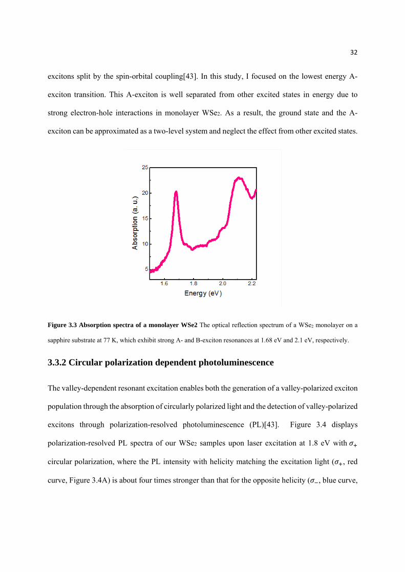
32
excitons split by the spin-orbital coupling[43]. In this study, I focused on the lowest energy A-
exciton transition. This A-exciton is well separated from other excited states in energy due to
strong electron-hole interactions in monolayer WSe2. As a result, the ground state and the A-
exciton can be approximated as a two-level system and neglect the effect from other excited states.
Figure 3.3 Absorption spectra of a monolayer WSe2 The optical reflection spectrum of a WSe2 monolayer on a
sapphire substrate at 77 K, which exhibit strong A- and B-exciton resonances at 1.68 eV and 2.1 eV, respectively.
3.3.2 Circular polarization dependent photoluminescence
The valley-dependent resonant excitation enables both the generation of a valley-polarized exciton
population through the absorption of circularly polarized light and the detection of valley-polarized
excitons through polarization-resolved photoluminescence (PL)[43]. Figure 3.4 displays
polarization-resolved PL spectra of our WSe2 samples upon laser excitation at 1.8 eV with
circular polarization, where the PL intensity with helicity matching the excitation light ( , red
curve, Figure 3.4A) is about four times stronger than that for the opposite helicity ( , blue curve,

33
Figure 3.4B). This behavior is similar to that reported in previous studies[43], and verifies the
valley-selective excitation and emission in our WSe2 monolayers. The non-zero polarized PL
is presumably due to a finite intervalley scattering because the excitation energy is ~120 meV
higher than the A-exciton resonance.
Figure 3.4 Circular polarization dependent photoluminescence spectra Polarization-resolved PL spectra of a
WSe2 monolayer at 77K. For 1.8 eV excitation laser with left circular polarization, the PL spectra show a prominent
emission peak at the A-exciton resonance (1.68 eV), and the PL intensity with left circular polarization (red curve, A)
is about four times stronger than that with right circular polarization (blue curve, B). It demonstrates that valley-
polarized A-exciton population can be created by circularly polarized resonant excitation, and it can be detected by
polarization-resolved PL spectroscopy.
3.3.3 Valley-selective optical Stark effect
I measured the valley-selective optical Stark shift in WSe2 monolayers with non-resonant
circularly polarized excitation using pump-probe spectroscopy as explained previously.
Femtosecond pump pulses with tunable photon energies below the A-exciton resonance were
generated by an optical parametric amplifier. Optical Stark shifts of the WSe2 exciton transitions
induced by the pump pulses was then probed in transient reflection spectra over the spectral range
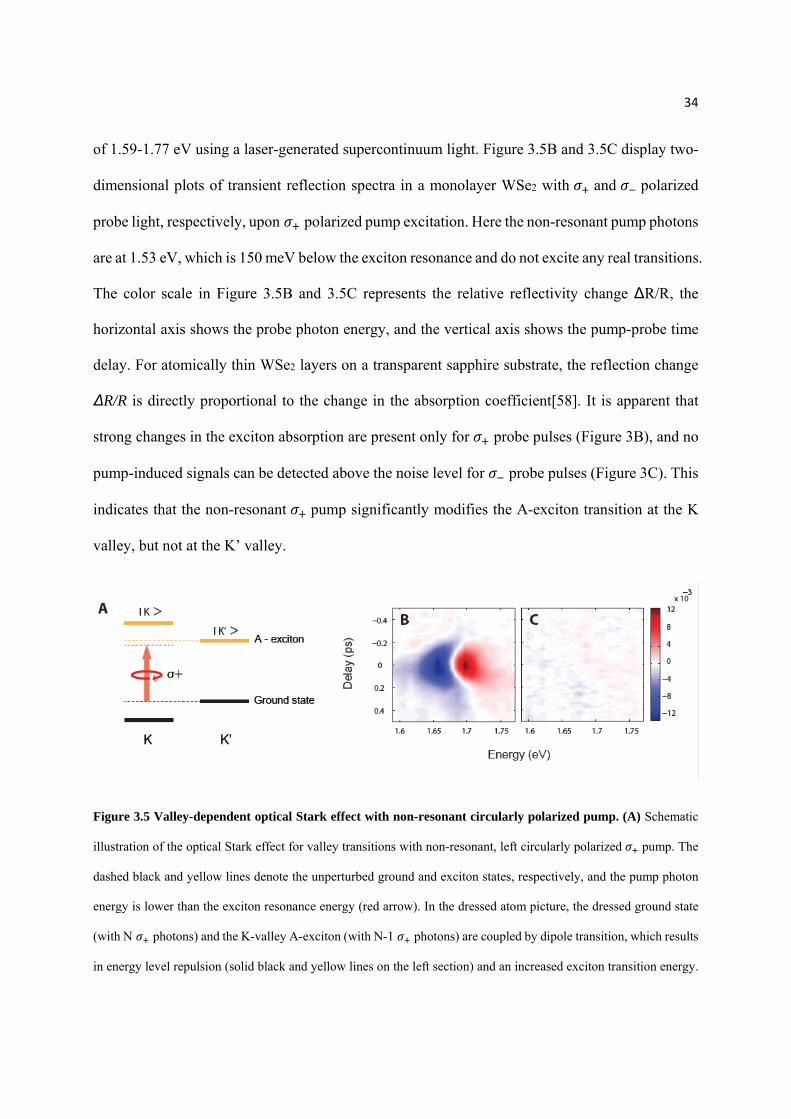
34
of 1.59-1.77 eV using a laser-generated supercontinuum light. Figure 3.5B and 3.5C display two-
dimensional plots of transient reflection spectra in a monolayer WSe2 with and polarized
probe light, respectively, upon polarized pump excitation. Here the non-resonant pump photons
are at 1.53 eV, which is 150 meV below the exciton resonance and do not excite any real transitions.
The color scale in Figure 3.5B and 3.5C represents the relative reflectivity change ∆R/R, the
horizontal axis shows the probe photon energy, and the vertical axis shows the pump-probe time
delay. For atomically thin WSe2 layers on a transparent sapphire substrate, the reflection change
∆R/R is directly proportional to the change in the absorption coefficient[58]. It is apparent that
strong changes in the exciton absorption are present only for probe pulses (Figure 3B), and no
pump-induced signals can be detected above the noise level for probe pulses (Figure 3C). This
indicates that the non-resonant pump significantly modifies the A-exciton transition at the K
valley, but not at the K’ valley.
Figure 3.5 Valley-dependent optical Stark effect with non-resonant circularly polarized pump. (A) Schematic
illustration of the optical Stark effect for valley transitions with non-resonant, left circularly polarized pump. The
dashed black and yellow lines denote the unperturbed ground and exciton states, respectively, and the pump photon
energy is lower than the exciton resonance energy (red arrow). In the dressed atom picture, the dressed ground state
(with N photons) and the K-valley A-exciton (with N-1 photons) are coupled by dipole transition, which results
in energy level repulsion (solid black and yellow lines on the left section) and an increased exciton transition energy.
35
On the other hand, pump does not affect K’-valley A-exciton resonance due to optical selection rule (right section).
(B) and (C) Transient reflection spectra of A-exciton resonance at 77 K. The color scale, horizontal axis, and vertical
axis represent the relative reflectivity change ∆R/R, the probe photon energy, and the pump-probe time delay,
respectively. For atomically thin WSe2 on sapphire substrate, ∆R/R is proportional to absorption change. Non-resonant
pump of photon energy at 1.53 eV leads to a strong transient absorption signal for probes with the same polarization
(B), but produces no transient response for probes with the opposite polarization (C). It demonstrates that non-
resonant pump significantly modifies A-exciton transition at the K valley, but not at the K’ valley.
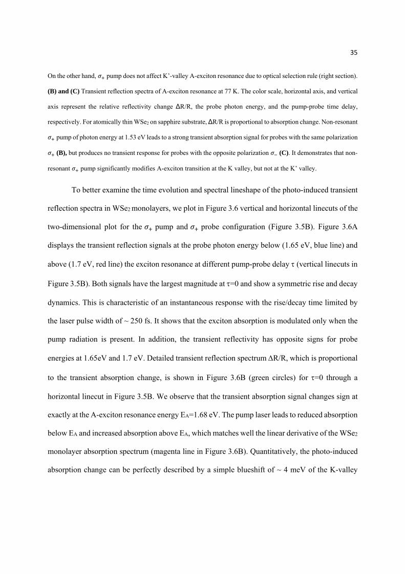
To better examine the time evolution and spectral lineshape of the photo-induced transient
reflection spectra in WSe2 monolayers, we plot in Figure 3.6 vertical and horizontal linecuts of the
two-dimensional plot for the pump and probe configuration (Figure 3.5B). Figure 3.6A
displays the transient reflection signals at the probe photon energy below (1.65 eV, blue line) and
above (1.7 eV, red line) the exciton resonance at different pump-probe delay (vertical linecuts in
Figure 3.5B). Both signals have the largest magnitude at =0 and show a symmetric rise and decay
dynamics. This is characteristic of an instantaneous response with the rise/decay time limited by
the laser pulse width of ~ 250 fs. It shows that the exciton absorption is modulated only when the
pump radiation is present. In addition, the transient reflectivity has opposite signs for probe
energies at 1.65eV and 1.7 eV. Detailed transient reflection spectrum R/R, which is proportional
to the transient absorption change, is shown in Figure 3.6B (green circles) for =0 through a
horizontal linecut in Figure 3.5B. We observe that the transient absorption signal changes sign at
exactly at the A-exciton resonance energy EA=1.68 eV. The pump laser leads to reduced absorption
below EA and increased absorption above EA, which matches well the linear derivative of the WSe2
monolayer absorption spectrum (magenta line in Figure 3.6B). Quantitatively, the photo-induced
absorption change can be perfectly described by a simple blueshift of ~ 4 meV of the K-valley
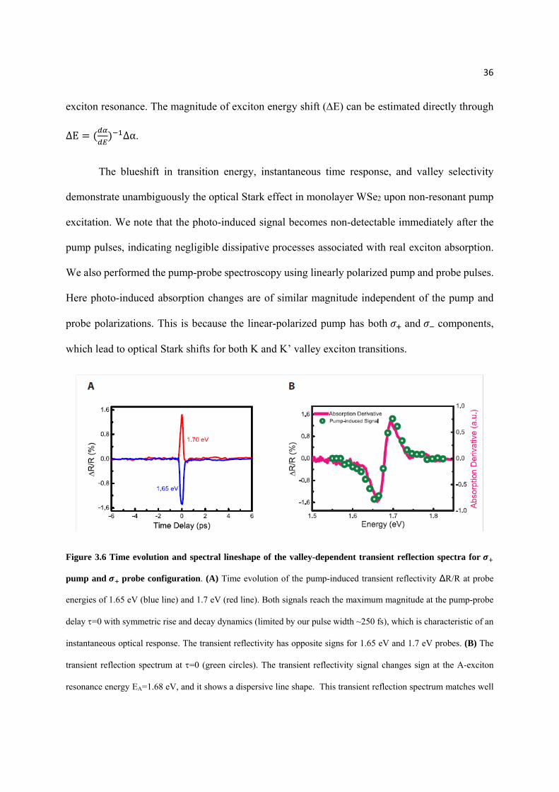
36
exciton resonance. The magnitude of exciton energy shift (E) can be estimated directly through
∆E ∆α.
The blueshift in transition energy, instantaneous time response, and valley selectivity
demonstrate unambiguously the optical Stark effect in monolayer WSe2 upon non-resonant pump
excitation. We note that the photo-induced signal becomes non-detectable immediately after the
pump pulses, indicating negligible dissipative processes associated with real exciton absorption.
We also performed the pump-probe spectroscopy using linearly polarized pump and probe pulses.
Here photo-induced absorption changes are of similar magnitude independent of the pump and
probe polarizations. This is because the linear-polarized pump has both and components,
which lead to optical Stark shifts for both K and K’ valley exciton transitions.
Figure 3.6 Time evolution and spectral lineshape of the valley-dependent transient reflection spectra for
pump and probe configuration. (A) Time evolution of the pump-induced transient reflectivity ∆R/R at probe
energies of 1.65 eV (blue line) and 1.7 eV (red line). Both signals reach the maximum magnitude at the pump-probe
delay =0 with symmetric rise and decay dynamics (limited by our pulse width ~250 fs), which is characteristic of an
instantaneous optical response. The transient reflectivity has opposite signs for 1.65 eV and 1.7 eV probes. (B) The
transient reflection spectrum at =0 (green circles). The transient reflectivity signal changes sign at the A-exciton
resonance energy EA=1.68 eV, and it shows a dispersive line shape. This transient reflection spectrum matches well

37
with the derivative of linear absorption spectrum in monolayer WSe2, and can be fully accounted for by a 4 meV
blueshift of the K-valley A-exciton resonance (magenta line).
3.3.4 Control of energy shift with pump power and detuning
Next I examine how the valley-selective optical Stark shift varies with the pump laser
intensity and detuning. The pump detuning Ω is defined as the difference between the exciton
resonance energy ( ) and the pump photon energy ( ). Figure 3.7 shows the transient
reflection data (left axis) and the corresponding energy shift of the A-exciton energy (right axis)
at the K valley for pump and probe configuration with different pump detuning (green dots
in Figure 3.7A) and pump intensities (green dots in Figure 3.7B). We observe that the optical Stark
shift is inversely proportional to the pump detuning (magenta dashed line in Figure 3.7A), and
scales linearly with the laser intensity (magenta dashed line in Figure 3.7B). Such scaling matches
well with the theoretical prediction of optical Stark shift δ 2 ∙ / Ω, where S is the
optical Stark shift constant related to the transition dipole moment and is the electric field of
the pump pulse[59]. From the experimental data, we can determine an optical Stark shift constant
S ~ 45 Debye2 for A-exciton in monolayer WSe2, which is of similar magnitude to that for exciton
transition in semiconductor quantum wells[60, 61].

38
Figure 3.7 Pump detuning and pump intensity dependence of the valley-selective optical Stark shift. (A) The
transient reflection signal at 1.7 eV (left axis) and the corresponding optical Stark shift (right axis) as a function of the
pump detuning energy (green dots). The dependence can be nicely described by an inverse proportional relationship
(magenta line). (B) The transient reflection signal at 1.7 eV (left axis) and the corresponding optical Stark shift (right
axis) as a function of the pump laser intensity (green dots), which shows a linear scaling behavior (magenta line). The
optical Stark shift can selectively shift the K-valley exciton transition by as much as 10 meV, which corresponds to a
valley pseudo-magnetic field of ~ 60 T.
3.3.5 Estimation of pseudomagnetic field magnitude
The valley-selective optical Stark shift breaks the degeneracy of valley exciton transitions
in monolayer WSe2 and defines an effective valley pseudo-magnetic field. In the experiment, the
photo-induced energy splitting between K and K’ exciton transitions can be as large as 10 meV
(Figure 3.7). The corresponding pseudo-magnetic field Beff for valley excitons can be estimated
by , where is the Bohr magneton and gex is the effective g-factor for valley
exciton transitions in WSe2. The effective exciton g-factor gex combines contributions from both
electrons and holes, and has a theoretically predicted value ~ 1.5 for WSe2[62, 63]. Using this g-
factor, we estimate a pseudo-magnetic field Beff as high as 60 T for a 10 meV splitting of valley
exciton transitions. A real magnetic field of this magnitude is difficult to achieve even with

39
superconducting magnets, but such a pseudo-magnetic field for MX2 valley excitons can be
produced conveniently and with femtosecond temporal control using light pulses.
3.4 Conclusion and outlook
In summary, I demonstrate that the optical Stark effect can generate ultrafast and ultrahigh
pseudo-magnetic field for valley excitons in MX2 layers. It has been reported recently that excitons
in different valleys in monolayer WSe2, resonantly excited by linear polarization light, can
maintain their phase coherence over extended time[48]. The valley-dependent optical Stark effect
offers a convenient and ultrafast way to lift the valley degeneracy and introduce a controlled phase
difference between the two valley states, therefore enabling coherent rotation of resonantly excited
valley polarizations with high fidelity. In analogy with spintronics, such coherent manipulation of
valley polarization can open up fascinating opportunities for valleytronics.

40
Chapter. 4 Ultrafast charge transfer in MoS2/WS2
heterostructure
4.1 Introduction
Atomically thin 2D crystals constitute a rich family of materials ranging from insulators
and semiconductors to semi-metals and superconductors[2]. Heterostructures from these 2D
materials offer a new platform for exploring new physics like superlattice Dirac points and
Hofstadter butterfly pattern[64-66], and new devices like tunnelling transistors[67], memory
devices[68] and ultrathin photodetectors[69]. Van der Waals heterostructures of semiconducting
MX2 layers are particularly exciting for optoelectronic and light harvesting applications because
many MX2 monolayers are direct-bandgap semiconductors[6, 7] with remarkably strong light-
matter interactions[69, 70]. And importantly, MX2 heterostructures are predicted to form type-II
heterojunctions that can assist efficient separation of photoexcited electrons and holes[71-74].
In type-II heterojunctions, the conduction band minimum and valence band maximum
reside in two separate materials. Photoexcited electrons and holes therefore prefer to stay at
separate locations. Figure 4.1 illustrates the alignment of electronic bands of MoS2 and WS2
monolayers predicted by a recent theory[73]. It shows that monolayer MoS2 and WS2 has a
bandgap of 2.39 eV and 2.31eV, respectively, and the MoS2 valence band maximum is 350 meV
lower than that of WS2. Consequently, the MoS2/WS2 heterostructure forms a type-II
heterojunction (if we neglect the hybridization of electronic states in MoS2 and WS2 layers), with

41
the conduction band minimum residing in MoS2 and the valence band maximum in WS2,
respectively. In the single-particle picture, this heterojunction will lead to efficient charge transfer
with separated electrons and holes in two layers upon optical excitation (Figure 4.1), which can
have a dominating effect on both light emission and photovoltaic responses in MoS2/WS2
heterostructures.
Figure 4.1 Band alignment and structure of MoS2/WS2 heterostructures. a. Schematics of theoretically predicted
band alignment of a MoS2/WS2 heterostructure, which forms a type-II heterojunction. Optical excitation of the MoS2
A-exciton will lead to layer separated electron and hole carriers.
There are two outstanding questions regarding charge transfer processes in the atomically
thin and van der Waals-coupled MoS2/WS2 heterostructure. (1) How do strong electron-electron
interactions and excitonic effects affect charge transfer processes? (2) How fast can charge transfer
take place between van der Waals-coupled layers? Electron-electron interactions are dramatically
enhanced in 2D materials due both to size confinement and inefficient screening. Theoretical
studies[75, 76] have predicted an exciton binding energy from 500 meV to 1 eV in MX2
monolayers, which is larger than the expected band displacement of 350 meV in MoS2/WS2

42
heterostructure. Therefore the exciton cannot dissociate into a free electron and a free hole in two
separate layers. Will this large exciton binding energy then prevent charge transfer processes and
keep the exciton in one layer, or will a new bound state of layer-separated electron and hole pair
be generated? In addition, van der Waals coupling is rather weak compared to covalent bonding.
Will that lead to a much slower charge transfer process in van der Waals heterostructures compared
to their covalent counterparts? Previous studies in organic photovoltaics (OPV)[77-79] have
shown that ultrafast charge transfer and separation can take place in organic/organic van der Waals
coupled interfaces. However, the 2D MX2 heterostructures possess two-dimensional crystalline
structures and atomically sharp interfaces, which is fundamentally different from the OPV
molecular systems. So far little is known about the ultrafast charge transfer dynamics in these new
2D heterostructures.
In this chapter, I study charge transfer dynamics in MoS2/WS2 heterolayers experimentally.
Through combined photoluminescence spectroscopy and optical pump-probe spectroscopy, we
demonstrate that ultrafast charge transfer takes place very efficiently in MoS2/WS2
heterostructures. In particular, holes in the MoS2 layer can separate into the WS2 layer within 50
fs upon photo-excitation.
4.2 Experiment
4.2.1 Photoluminescence and Raman spectrum measurement
For photoluminescence mapping, I use a 532 nm laser (photon energy =2.33 eV) to excite
the isolated monolayers of MoS2, WS2, and MoS2/WS2 heterostructures. The laser beam is focused

43
to a diffraction-limited spot with a diameter ~ 1 m, and the PL is collected in the reflection
geometry via confocal microscope. A monochrometer and a liquid nitrogen cooled CCD are used
to record the PL spectra. Two-dimensional PL mapping is done by scanning the computer-
controlled piezoelectric stage. For Raman measurements, we use a 488 nm excitation laser.
4.2.2 (Transient) Absorption spectrum measurement
I use the same experimental configuration as described in chapter 3.
4.2.3 Heterostructure preparation
The heterostructure was prepared by transferring[80] monolayer MoS2 onto monolayer
WS2 on sapphire. The CVD grown MoS2 single layer (described above) on SiO2/Si is spin-coated
with PMMA (A4) at 4000 rpm for 60 seconds. PMMA/ MoS2 film is separated from the substrate
(SiO2/Si) by KOH etching (1 mol/L) at 80 ˚C. The film is transferred to DI water beakers to dilute
KOH residue under MoS2. Then, it is transferred on to CVD grown WS2 on sapphire substrate
(described above) and soaked in acetone to dissolve PMMA. Finally, heterostructure sample is
annealed at elevated temperature in vacuum. Note there is no polymer between the MoS2 and WS2
layers in our sample after the PMMA transfer (PMMA was on top of the top layer), and they can
form fairly good contract.
4.3 Result and discussion
4.3.1 Optical micrograph of sample and Raman spectra
Figure 4.2a schematically shows our sample configuration. In brief, MoS2 monolayers

44
were grown on 285 nm SiO2/Si substrates using the chemical vapour deposition (CVD)
method[80]. They were subsequently transferred on top of as-grown CVD WS2 flakes on sapphire
substrates[81] to form MoS2/WS2 heterostructures. Raman spectra (Figure 4.2b) from isolated
MoS2 and WS2 films confirm that both are monolayers because the energy separation between
Raman active modes agrees well with previous reported values for monolayer MoS2 and WS2.[82-
85] The Raman spectrum of a MoS2/WS2 heterostructure (Figure 4.2b) appears to be an addition
of Raman modes from the constituent layers.
Figure 4.2 Schematic of heterostructure and Raman spectra a. Illustration of a MoS2/WS2 heterostructure with a
MoS2 monolayer lying on top of a WS2 monolayer. Electrons and holes created by light are shown to separate into
different layers. b. Raman spectra of an isolated MoS2 monolayer (blue trace), an isolated WS2 monolayer (red trace),
and a MoS2/WS2 heterostructure (black trace).
4.3.2 Photoluminescence spectrum and mapping of heterostructure
One sensitive probe of charge transfer in MX2 heterostructures is photoluminescence (PL)
spectroscopy, because an electron and hole pair spatially separated in two MX2 layers cannot emit
efficiently. We performed PL spectroscopy and mapping on multiple MoS2/WS2 heterostructure
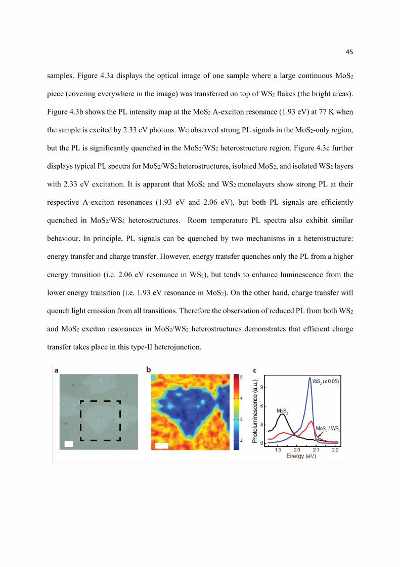
45
samples. Figure 4.3a displays the optical image of one sample where a large continuous MoS2
piece (covering everywhere in the image) was transferred on top of WS2 flakes (the bright areas).
Figure 4.3b shows the PL intensity map at the MoS2 A-exciton resonance (1.93 eV) at 77 K when
the sample is excited by 2.33 eV photons. We observed strong PL signals in the MoS2-only region,
but the PL is significantly quenched in the MoS2/WS2 heterostructure region. Figure 4.3c further
displays typical PL spectra for MoS2/WS2 heterostructures, isolated MoS2, and isolated WS2 layers
with 2.33 eV excitation. It is apparent that MoS2 and WS2 monolayers show strong PL at their
respective A-exciton resonances (1.93 eV and 2.06 eV), but both PL signals are efficiently
quenched in MoS2/WS2 heterostructures. Room temperature PL spectra also exhibit similar
behaviour. In principle, PL signals can be quenched by two mechanisms in a heterostructure:
energy transfer and charge transfer. However, energy transfer quenches only the PL from a higher
energy transition (i.e. 2.06 eV resonance in WS2), but tends to enhance luminescence from the
lower energy transition (i.e. 1.93 eV resonance in MoS2). On the other hand, charge transfer will
quench light emission from all transitions. Therefore the observation of reduced PL from both WS2
and MoS2 exciton resonances in MoS2/WS2 heterostructures demonstrates that efficient charge
transfer takes place in this type-II heterojunction.

46
Figure 4.3 Photoluminescence (PL) spectra and mapping of MoS2/WS2 heterostructures at 77 K. a. Optical
microscope image of a typical MoS2/WS2 heterostructure sample. The MoS2 layer covers everywhere in the image,
and bright areas correspond to MoS2/WS2 heterostructures. b. PL mapping data taken in the dashed rectangle area in
a. The colour scale represents PL intensity at the MoS2 A-exciton resonance (1.93 eV). It clearly shows that MoS2 PL
is strongly quenched in the heterostructure. Scale bar is 5 µm. c. Typical PL spectra of an isolated monolayer MoS2,
an isolated monolayer WS2 and a MoS2/WS2 heterostructure. The isolated MoS2 and WS2 monolayer show strong PL
at 1.93 eV and 2.06 eV, respectively, corresponding to their A-exciton resonances. Both exciton PL signals are
strongly quenched in the MoS2/WS2 heterostructure, suggesting an efficient charge transfer process exists in the
heterostructure.
4.3.3 Transient absorption measurement
To directly probe the charge transfer process and its ultrafast dynamics, we measured
transient absorption spectra of MoS2/WS2 heterostructures using resonant pump-probe
spectroscopy. A femtosecond pulse first excites the heterostructure, and the photo-induced changes
in the reflection spectrum (∆R/R) are probed by a laser-generated supercontinuum light after
controlled time delays. For atomically thin heterostructures on a transparent sapphire substrate, the
reflection change ∆R/R is directly proportional to the change in absorption coefficient. MoS2 and
WS2 monolayers have distinctly different exciton transitions. Therefore we can selectively excite
the MoS2 or WS2 layer using specific resonant optical excitations, and probe the accumulation of
electrons and holes in different layers through photo-induced changes in their respective exciton
transitions. Specifically, we choose a pump photon energy at 1.86 eV to excite exclusively the A-
exciton transition of MoS2. This pump cannot excite WS2 directly because the photon energy is
far below the absorption threshold of WS2. Afterwards we examine the photoinduced changes of
both WS2 and MoS2 exciton resonances in transient absorption spectra from 2.0-2.5 eV to probe
the charge distribution in heterostructures.
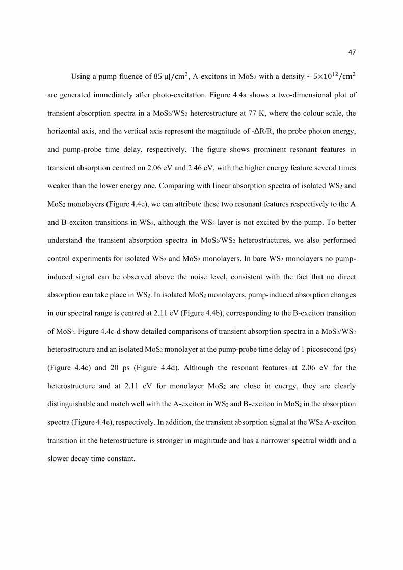
47
Using a pump fluence of 85μJ/cm2, A-excitons in MoS2 with a density ~ 5 1012/cm2
are generated immediately after photo-excitation. Figure 4.4a shows a two-dimensional plot of
transient absorption spectra in a MoS2/WS2 heterostructure at 77 K, where the colour scale, the
horizontal axis, and the vertical axis represent the magnitude of -∆R/R, the probe photon energy,
and pump-probe time delay, respectively. The figure shows prominent resonant features in
transient absorption centred on 2.06 eV and 2.46 eV, with the higher energy feature several times
weaker than the lower energy one. Comparing with linear absorption spectra of isolated WS2 and
MoS2 monolayers (Figure 4.4e), we can attribute these two resonant features respectively to the A
and B-exciton transitions in WS2, although the WS2 layer is not excited by the pump. To better
understand the transient absorption spectra in MoS2/WS2 heterostructures, we also performed
control experiments for isolated WS2 and MoS2 monolayers. In bare WS2 monolayers no pump-
induced signal can be observed above the noise level, consistent with the fact that no direct
absorption can take place in WS2. In isolated MoS2 monolayers, pump-induced absorption changes
in our spectral range is centred at 2.11 eV (Figure 4.4b), corresponding to the B-exciton transition
of MoS2. Figure 4.4c-d show detailed comparisons of transient absorption spectra in a MoS2/WS2
heterostructure and an isolated MoS2 monolayer at the pump-probe time delay of 1 picosecond (ps)
(Figure 4.4c) and 20 ps (Figure 4.4d). Although the resonant features at 2.06 eV for the
heterostructure and at 2.11 eV for monolayer MoS2 are close in energy, they are clearly
distinguishable and match well with the A-exciton in WS2 and B-exciton in MoS2 in the absorption
spectra (Figure 4.4e), respectively. In addition, the transient absorption signal at the WS2 A-exciton
transition in the heterostructure is stronger in magnitude and has a narrower spectral width and a
slower decay time constant.

48
Figure 4.4 Transient absorption spectra of MoS2/WS2 heterostructures. a. and b. Two-dimensional plots of
transient absorption spectra at 77 K from a MoS2/WS2 heterostructure (a) and an isolated MoS2 monolayer (b) upon
excitation of the MoS2 A-exciton transitions. The horizontal axis, vertical axis, and colour scale represent the probe
photon energy, pump-probe time delay, and the transient absorption signal, respectively. Positive signals indicate a
pump-induced decrease in absorption. c. and d. Transient absorption spectra for MoS2/WS2 (red circles) and MoS2
(green square) at 1 ps and 20 ps pump-probe delay, respectively. e. Linear absorption spectra of monolayers of MoS2
(magenta line) and WS2 (blue line). Although only MoS2 A-exciton transitions are optically excited, transient
absorption spectra in the MoS2/WS2 heterostructure are dominated by a resonance feature (red circles in c and d)
corresponding to the WS2 A-exciton transition (blue line in e), which is clearly distinguishable from the resonance
feature corresponding to the MoS2 B-exciton transition in an isolated MoS2 monolayer (green squares in c and d and
magenta line in e). It demonstrates unambiguously an efficient hole transfer from the photoexcited MoS2 layer to the
WS2 layer in MoS2/WS2 heterostructures.
Our transient absorption measurements of MoS2/WS2 heterostructures establish
unambiguously that optical excitation in MoS2 leads to strong modification of exciton transitions
in WS2, which has a larger optical bandgap. It provides direct evidence of efficient charge
separation in photo-excited MoS2/WS2 heterostructures as described in Figure 4.1: electron hole

49
pairs are initially created in the MoS2 layer, but holes quickly transfer to the WS2 layer due to the
type-II band alignment, while electrons stay in the MoS2 layer. The photo-excited electrons in
MoS2 and holes in WS2 lead to strong transient absorption signal for exciton transitions in both
MoS2 and WS2. Transient absorption signals are the strongest for the A-excitons due to their
sharper resonances and efficient photo-bleaching effects from Pauli blocking, but B-exciton
transitions are also affected. Consequently, the transient absorption spectra in MoS2/WS2
heterostructures are dominated by the A-exciton transition in WS2. Photo-induced changes of B-
exciton transitions in the MoS2/WS2 heterostructure (Figure 4.4a) and in the MoS2 monolayer
(Figure 4.4b) can also be identified, but they are significantly weaker than that of A-exciton
transitions. Room temperature data show similar.
4.3.4 Determination of charge transfer time
The rise time of the WS2 A-exciton transient absorption signal probes directly the hole
transfer dynamics from the MoS2 layer because this signal exists only after the hole transfer, but
not right at the excitation of MoS2. Figure 4.5 shows the dynamic evolution of the WS2 A-exciton
resonance in the MoS2/WS2 heterostructure (Figure 4.5a), which can be compared to the transient
absorption signal for the B-exciton resonance in an isolated MoS2 monolayer (Figure 4.5b). We
found that the rise time in both signals are almost identical, and it is limited by the laser pulse
duration ~ 250 fs. In Figure 4b the MoS2 monolayer is directly pumped, and the photo-induced
signal should appear instantaneously. (The rise time of pump-induced A exciton and B exciton
signals in MoS2 has indistinguishable behavior.) We could reproduce the ultrafast dynamics in the
MoS2 monolayer in Figure 4.5b by convoluting the instrument response function (the blue dashed
curve in Figure 4.5b) with an instantaneous response in MoS2. Using the same instrument response
function for time convolution, we can then reproduce the experimentally observed signal in the
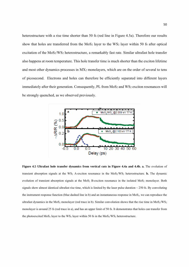
50
heterostructure with a rise time shorter than 50 fs (red line in Figure 4.5a). Therefore our results
show that holes are transferred from the MoS2 layer to the WS2 layer within 50 fs after optical
excitation of the MoS2/WS2 heterostructure, a remarkably fast rate. Similar ultrafast hole transfer
also happens at room temperature. This hole transfer time is much shorter than the exciton lifetime
and most other dynamics processes in MX2 monolayers, which are on the order of several to tens
of picosecond. Electrons and holes can therefore be efficiently separated into different layers
immediately after their generation. Consequently, PL from MoS2 and WS2 exciton resonances will
be strongly quenched, as we observed previously.
Figure 4.5 Ultrafast hole transfer dynamics from vertical cuts in Figure 4.4a and 4.4b. a. The evolution of
transient absorption signals at the WS2 A-exciton resonance in the MoS2/WS2 heterostructure. b. The dynamic
evolution of transient absorption signals at the MoS2 B-exciton resonance in the isolated MoS2 monolayer. Both
signals show almost identical ultrafast rise time, which is limited by the laser pulse duration ~ 250 fs. By convoluting
the instrument response function (blue dashed line in b) and an instantaneous response in MoS2, we can reproduce the
ultrafast dynamics in the MoS2 monolayer (red trace in b). Similar convolution shows that the rise time in MoS2/WS2
monolayer is around 25 fs (red trace in a), and has an upper limit of 50 fs. It demonstrates that holes can transfer from
the photoexcited MoS2 layer to the WS2 layer within 50 fs in the MoS2/WS2 heterostructure.

51
4.3.5 Effect of Coulomb interaction and lattice mismatch on charge transfer
dynamics
Our experimental data establishes that charge separation in MoS2/WS2 heterostructures is
very efficient, although the band offset between MoS2 and WS2 is smaller than the predicted
exciton binding energy in monolayer MX2. Energetically uncorrelated free electrons and holes in
separated MoS2 and WS2 layers cannot be produced through the excitation of MoS2 A-excitons.
However, the MoS2 and WS2 layers are only ~0.62 nm separated from each other[72], suggesting
that even for layer-separated electrons and holes, strong Coulomb interactions can lead to bound
exciton states. These exciton states with electron and hole residing in different layers can be
energetically favourable compared to an exciton confined to only MoS2 layer, and are likely to be
responsible for the efficient charge separation observed in MoS2/WS2 heterostructures. Such
bounded excitons with electron and hole in different materials, known as charge transfer excitons
(CTC), have also been investigated in other type-II heterojunctions, such as molecular
donor/acceptor interfaces in the context of organic photovoltaics[77, 78, 86].
The observed sub-50 fs hole transfer time is remarkably short considering that the MoS2
and WS2 layers are twisted relative to each other and are coupled by relatively weak van der Waals
interactions. One factor contributing to the ultrafast charge transfer rate in atomically thin
heterostructures is the close proximity of the two heterolayers, because electrons or holes only
need to move less than 1 nm vertically for the charge transfer process to happen. Still, the 50 fs
hole transfer time for van der Waals heterostructures is fast. Microscopic understanding of this
ultrafast hole transfer in MX2 heterostructures requires detailed theoretical studies to examine the
hybridization of electronic states in twisted heterolayers and the dynamic evolution of photo-
excited states due to electron-phonon and electron-electron interactions. For example, because
52
MoS2/WS2 heterostructures are extended crystalline 2D layers, resonant charge transfer has to
satisfy both energy and momentum conservations, and electronic coupling between states with
different momenta in the Brillouin zone can vary significantly. It is known that for MoS2 bilayers,
electronic coupling at the K point in the Brillouin zone is weak. Electron wavefunction
hybridization at the Γ point, however, is much stronger, which leads to a rise in Γ point valence
band and an indirect bandgap in bilayer MoS2.[6, 7] Electronic coupling between incommensurate
MoS2 and WS2 can play an important role in the charge transfer dynamics of twisted MoS2/WS2
heterostructures, the behaviour of which has been little studied so far. Because van der Waals
heterostructures have atomically sharp interfaces with no dangling bonds and well-defined optical
resonances, they provide an ideal model system for further experimental and theoretical
investigations of interfacial charge transfer processes and the charge transfer exciton states.
The ultrafast charge transfer process in atomically thin MX2 heterostructures has important
implications for photonic and optoelectronic applications. MX2 semiconductors have extremely
strong optical absorption, and has been considered previously for photodetectors[69],
photovoltaics[87] and photocatalysis[88]. Compared with organic photovoltaic materials, these 2D
layers have crystalline structure and better electrical transport properties. Our studies here show
that the type-II MX2 heterostructures also exhibit femtosecond charge transfer rate, which provides
an ideal way to spatially separate electrons and holes for electrical collection and utilization.
4.4 Conclusions and outlook
In summary, I have demonstrated for the first time efficient charge transfer in MoS2/WS2
heterostructures through combined PL mapping and transient absorption measurement. We

53
quantitatively determine the ultrafast hole transfer time to be less than 50 fs. Our study suggests
that MX2 heterostructures, with their remarkable electrical and optical properties and rapid
development of large area synthesis, hold great promise for future optoelectronic and photovoltaic
applications.
54
Bibliography
1. Geim, A.K. and K.S. Novoselov, The rise of graphene. Nat Mater, 2007. 6(3): p. 183-
191.
2. Geim, A.K. and I.V. Grigorieva, Van der Waals heterostructures. Nature, 2013.
499(7459): p. 419-425.
3. Mak, K.F., et al., Optical spectroscopy of graphene: From the far infrared to the
ultraviolet. Solid State Communications, 2012. 152(15): p. 1341-1349.
4. Wang, F., et al., Gate-Variable Optical Transitions in Graphene. Science, 2008.
320(5873): p. 206-209.
5. Horng, J., et al., Drude conductivity of Dirac fermions in graphene. Physical Review B,
2011. 83(16): p. 165113.
6. Splendiani, A., et al., Emerging Photoluminescence in Monolayer MoS2. Nano Letters,
2010. 10(4): p. 1271-1275.
7. Mak, K.F., et al., Atomically thin MoS 2: a new direct-gap semiconductor. Physical
Review Letters, 2010. 105(13): p. 136805.
8. Xiao, D., et al., Coupled Spin and Valley Physics in Monolayers of MoS2 and Other
Group-VI Dichalcogenides. Physical Review Letters, 2012. 108(19).
9. Chernikov, A., et al., Exciton Binding Energy and Nonhydrogenic Rydberg Series in
Monolayer $\mathrmWS_2$. Physical Review Letters, 2014. 113(7): p. 076802.
10. Ye, Z., et al., Probing excitonic dark states in single-layer tungsten disulphide. Nature,
2014. 513(7517): p. 214-218.
11. Ugeda, M.M., et al., Giant bandgap renormalization and excitonic effects in a monolayer
transition metal dichalcogenide semiconductor. Nat Mater, 2014. 13(12): p. 1091-1095.

55
12. Gunawan, O., et al., Valley Susceptibility of an Interacting Two-Dimensional Electron
System. Physical Review Letters, 2006. 97(18): p. 186404.
13. Nair, R.R., et al., Fine Structure Constant Defines Visual Transparency of Graphene.
Science, 2008. 320(5881): p. 1308.
14. Mak, K.F., et al., Measurement of the Optical Conductivity of Graphene. Physical
Review Letters, 2008. 101(19): p. 196405.
15. Li, Z.Q., et al., Dirac charge dynamics in graphene by infrared spectroscopy. Nat Phys,
2008. 4(7): p. 532-535.
16. Schuller, J.A., et al., Plasmonics for extreme light concentration and manipulation. Nat
Mater, 2010. 9(3): p. 193-204.
17. Mühlschlegel, P., et al., Resonant Optical Antennas. Science, 2005. 308(5728): p. 1607-
1609.
18. Lezec, H.J., J.A. Dionne, and H.A. Atwater, Negative Refraction at Visible Frequencies.
Science, 2007. 316(5823): p. 430-432.
19. Valentine, J., et al., Three-dimensional optical metamaterial with a negative refractive
index. Nature, 2008. 455(7211): p. 376-379.
20. Chen, H.-T., et al., Active terahertz metamaterial devices. Nature, 2006. 444(7119): p.
597-600.
21. Chen, H.-T., et al., A metamaterial solid-state terahertz phase modulator. Nat Photon,
2009. 3(3): p. 148-151.
22. Chen, H.-T., et al., Electronic control of extraordinaryterahertz transmission
throughsubwavelength metal hole arrays. Opt. Express, 2008. 16(11): p. 7641-7648.
23. Yu, P.Y. and M. Cardona, Fundamentals of Semiconductors. 2004: p. p. 305.

56
24. Novoselov, K.S., et al., Two-dimensional gas of massless Dirac fermions in graphene.
Nature, 2005. 438(7065): p. 197-200.
25. Zhang, Y., et al., Experimental observation of the quantum Hall effect and Berry's phase
in graphene. Nature, 2005. 438(7065): p. 201-204.
26. Papasimakis, N., et al., Graphene in a photonic metamaterial. Opt. Express, 2010. 18(8):
p. 8353-8359.
27. Liu, M., et al., A graphene-based broadband optical modulator. Nature, 2011.
474(7349): p. 64-67.
28. Xia, F., et al., Ultrafast graphene photodetector. Nat Nano, 2009. 4(12): p. 839-843.
29. Ju, L., et al., Graphene plasmonics for tunable terahertz metamaterials. Nat Nano, 2011.
6(10): p. 630-634.
30. Yan, H., et al., Tunable infrared plasmonic devices using graphene/insulator stacks. Nat
Nano, 2012. 7(5): p. 330-334.
31. Fei, Z., et al., Gate-tuning of graphene plasmons revealed by infrared nano-imaging.
ArXiv:1202.4993v2, 2012.
32. Echtermeyer, T.J., et al., Strong plasmonic enhancement of photovoltage in graphene.
Nat Commun, 2011. 2: p. 458.
33. Liu, Y., et al., Plasmon resonance enhanced multicolour photodetection by graphene.
Nat Commun, 2011. 2: p. 579.
34. Dawlaty, J.M., et al., Measurement of the optical absorption spectra of epitaxial
graphene from terahertz to visible. Applied Physics Letters, 2008. 93(13): p. 131905.
35. Gusynin, V.P., S.G. Sharapov, and J.P. Carbotte, Sum rules for the optical and Hall
conductivity in graphene. Physical Review B, 2007. 75(16): p. 165407.

57
36. Link, S. and M.A. El-Sayed, Spectral Properties and Relaxation Dynamics of Surface
Plasmon Electronic Oscillations in Gold and Silver Nanodots and Nanorods. The Journal
of Physical Chemistry B, 1999. 103(40): p. 8410-8426.
37. Kim, K.S., et al., Large-scale pattern growth of graphene films for stretchable
transparent electrodes. Nature, 2009. 457(7230): p. 706-710.
38. Li, X., et al., Large-Area Synthesis of High-Quality and Uniform Graphene Films on
Copper Foils. Science, 2009. 324(5932): p. 1312-1314.
39. Zou, Y., et al., Interaction between graphene and metamaterials: split rings vs. wire
pairs. Opt. Express, 2012. 20(11): p. 12198-12204.
40. Noda, S., M. Fujita, and T. Asano, Spontaneous-emission control by photonic crystals
and nanocavities. Nat Photon, 2007. 1(8): p. 449-458.
41. Faraon, A., et al., Fast Electrical Control of a Quantum Dot Strongly Coupled to a
Photonic-Crystal Cavity. Physical Review Letters, 2010. 104(4): p. 047402.
42. Sukang, B., et al., 30-Inch Roll-Based Production of High-Quality Graphene Films for
Flexible Transparent Electrodes. CORD Conference Proceedings, 2009.
43. Xu, X., et al., Spin and pseudospins in layered transition metal dichalcogenides. Nat
Phys, 2014. 10: p. 343.
44. Wang, Q.H., et al., Electronics and optoelectronics of two-dimensional transition metal
dichalcogenides. Nature Nanotechnology, 2012. 7(11): p. 699-712.
45. Cao, T., et al., Valley-selective circular dichroism of monolayer molybdenum disulphide.
Nature Communications, 2012. 3.
46. Mak, K.F., et al., Control of valley polarization in monolayer MoS2 by optical helicity.
Nature Nanotechnology, 2012. 7(8): p. 494-498.

58
47. Zeng, H.L., et al., Valley polarization in MoS2 monolayers by optical pumping. Nature
Nanotechnology, 2012. 7(8): p. 490-493.
48. Jones, A.M., et al., Optical generation of excitonic valley coherence in monolayer WSe2.
Nature Nanotechnology, 2013. 8(9): p. 634-638.
49. Zhang, Y.J., et al., Electrically Switchable Chiral Light-Emitting Transistor. Science,
2014. 344(6185): p. 725-728.
50. Mak, K.F., et al., The valley Hall effect in MoS2 transistors. Science, 2014. 344(6191): p.
1489-1492.
51. Poole, C.P., Electron spin resonance 2nd edn (Wiley, New York, 1983)
52. Koppens, F.H.L., et al., Driven coherent oscillations of a single electron spin in a
quantum dot. Nature, 2006. 442(7104): p. 766-771.
53. Gupta, J.A., et al., Ultrafast manipulation of electron spin coherence. Science, 2001.
292(5526): p. 2458-2461.
54. Press, D., et al., Complete quantum control of a single quantum dot spin using ultrafast
optical pulses. Nature, 2008. 456(7219): p. 218-221.
55. Shi, H., et al., Exciton Dynamics in Suspended Monolayer and Few-Layer MoS2 2D
Crystals. ACS Nano, 2012. 7(2): p. 1072-1080.
56. Wang, Q., et al., Valley Carrier Dynamics in Monolayer Molybdenum Disulfide from
Helicity-Resolved Ultrafast Pump–Probe Spectroscopy. ACS Nano, 2013. 7(12): p.
11087-11093.
57. Sie, E.J., et al., Biexciton formation in monolayer MoS2 observed by transient absorption
spectroscopy. arXiv preprint arXiv:1312.2918, 2013.

59
58. Mak, K.F., et al., Measurement of the Optical Conductivity of Graphene. Physical
Review Letters, 2008. 101(19).
59. Cohentannoudji, C. and S. Reynaud, Dressed-atom description of resonance fluorescence
and absorption-spectra of a multilevel atom in an intense laser-beam. Journal of Physics
B-Atomic Molecular and Optical Physics, 1977. 10(3): p. 345-363.
60. Shen, Y.-R., The principles of nonlinear optics. New York, Wiley-Interscience, 1984,
1984. 1.
61. Von Lehmen, A., et al., Optical Stark effect on excitons in GaAs quantum wells. Optics
Letters, 1986. 11(10): p. 609-611.
62. Rostami, H., A.G. Moghaddam, and R. Asgari, Effective lattice Hamiltonian for
monolayer MoS2: Tailoring electronic structure with perpendicular electric and
magnetic fields. Physical Review B, 2013. 88(8).
63. Shi, H.L., et al., Quasiparticle band structures and optical properties of strained
monolayer MoS2 and WS2. Physical Review B, 2013. 87(15).
64. Ponomarenko, L.A., et al., Cloning of Dirac fermions in graphene superlattices. Nature,
2013. 497(7451): p. 594-597.
65. Hunt, B., et al., Massive Dirac Fermions and Hofstadter Butterfly in a van der Waals
Heterostructure. Science, 2013. 340(6139): p. 1427-1430.
66. Dean, C.R., et al., Hofstadter/'s butterfly and the fractal quantum Hall effect in moire
superlattices. Nature, 2013. 497(7451): p. 598-602.
67. Britnell, L., et al., Field-Effect Tunneling Transistor Based on Vertical Graphene
Heterostructures. Science, 2012. 335(6071): p. 947-950.

60
68. Sup Choi, M., et al., Controlled charge trapping by molybdenum disulphide and
graphene in ultrathin heterostructured memory devices. Nat Commun, 2013. 4: p. 1624.
69. Britnell, L., et al., Strong Light-Matter Interactions in Heterostructures of Atomically
Thin Films. Science, 2013. 340(6138): p. 1311-1314.
70. Lopez-Sanchez, O., et al., Ultrasensitive photodetectors based on monolayer MoS2. Nat
Nano, 2013. 8(7): p. 497-501.
71. Gong, C., et al., Band alignment of two-dimensional transition metal dichalcogenides:
Application in tunnel field effect transistors. Applied Physics Letters, 2013. 103(5): p.
053513.
72. Komsa, H.-P. and A.V. Krasheninnikov, Electronic structures and optical properties of
realistic transition metal dichalcogenide heterostructures from first principles. Physical
Review B, 2013. 88(8): p. 085318.
73. Kang, J., et al., Band offsets and heterostructures of two-dimensional semiconductors.
Applied Physics Letters, 2013. 102(1): p. 012111.
74. Terrones, H., F. López-Urías, and M. Terrones, Novel hetero-layered materials with
tunable direct band gaps by sandwiching different metal disulfides and diselenides. Sci.
Rep., 2013. 3.
75. Berkelbach, T.C., M.S. Hybertsen, and D.R. Reichman, Theory of neutral and charged
excitons in monolayer transition metal dichalcogenides. Physical Review B, 2013. 88(4):
p. 045318.
76. Qiu, D.Y., F.H. da Jornada, and S.G. Louie, Optical Spectrum of
$\mathrmMoS_2$: Many-Body Effects and Diversity of Exciton States. Physical
Review Letters, 2013. 111(21): p. 216805.
61
77. Grancini, G., et al., Hot exciton dissociation in polymer solar cells. Nat Mater, 2013.
12(1): p. 29-33.
78. Jailaubekov, A.E., et al., Hot charge-transfer excitons set the time limit for charge
separation at donor/acceptor interfaces in organic photovoltaics. Nat Mater, 2013. 12(1):
p. 66-73.
79. Kaake, L.G., D. Moses, and A.J. Heeger, Coherence and uncertainty in nanostructured
organic photovoltaics. The Journal of Physical Chemistry Letters, 2013. 4(14): p. 2264-
2268.
80. van der Zande, A.M., et al., Grains and grain boundaries in highly crystalline monolayer
molybdenum disulphide. Nature materials, 2013. 12(6): p. 554-561.
81. Zhang, Y., et al., Controlled growth of high-quality monolayer WS2 layers on sapphire
and imaging its grain boundary. ACS nano, 2013. 7(10): p. 8963-8971.
82. Lee, C., et al., Anomalous lattice vibrations of single-and few-layer MoS2. ACS nano,
2010. 4(5): p. 2695-2700.
83. Berkdemir, A., et al., Identification of individual and few layers of WS2 using Raman
Spectroscopy. Scientific reports, 2013. 3.
84. Luo, X., et al., Effects of lower symmetry and dimensionality on Raman spectra in two-
dimensional WSe 2. Physical Review B, 2013. 88(19): p. 195313.
85. Terrones, H., et al., New first order Raman-active modes in few layered transition metal
dichalcogenides. Scientific reports, 2014. 4.
86. Gélinas, S., et al., Ultrafast long-range charge separation in organic semiconductor
photovoltaic diodes. Science, 2014. 343(6170): p. 512-516.
62
87. Gourmelon, E., et al., MS 2 (M= W, Mo) photosensitive thin films for solar cells. Solar
Energy Materials and Solar Cells, 1997. 46(2): p. 115-121.
88. Ho, W., et al., Preparation and photocatalytic behavior of MoS2 and WS2 nanocluster
sensitized TiO2. Langmuir, 2004. 20(14): p. 5865-5869.


