Cellular Antenna Switches for Multimode Applications Based on a Silicon-On-Insulator (S-O-I) Technology Ali Tombak, Christian Iversen, Jean-Blaise Pierres, Dan Kerr, Mike Carroll, Phil Mason, Eddie Spears and Todd Cillenwater
• Motivation
• Silicon-on-Insulator (SOI) for Antenna Switches
• Design of High Order Switches on SOI
• Small Signal Measurements
• Harmonics and IMD Performance
• Spurious Emissions
• Summary and Conclusions
Outline
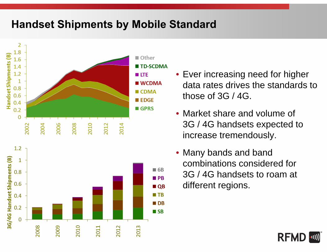
• Ever increasing need for higher data rates drives the standards to those of 3G / 4G.
• Market share and volume of 3G / 4G handsets expected to increase tremendously.
• Many bands and band combinations considered for 3G / 4G handsets to roam at different regions.
Handset Shipments by Mobile Standard

• 3G / 4G system architectures require a complex integration of switch, filter, and duplex functions in the front-end.
GSM RX1
GSM RX2
GSM RX3
GSM RX4
GSM 1800/1900
GSM 850/900
UMTS1 TX
UMTS2 TX
UMTS3 TX
UMTS3 RX
UMTS2 RX
UMTS1 RX
Duplexer 2
Duplexer 3
Duplexer 1
RX SAW FiltersSP9T Switch
GSM TX Filters
Control Lines
3G/4G Front End Architectures
Switch Duplexer Module
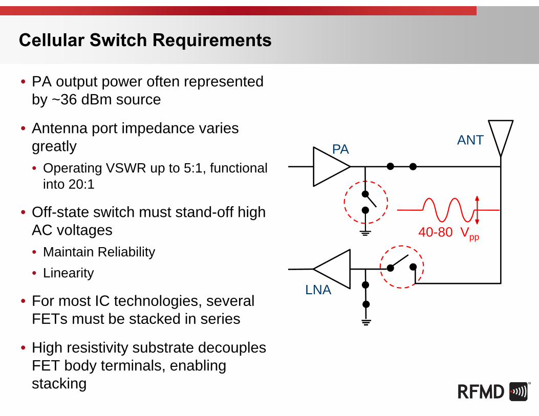
• PA output power often represented by ~36 dBm source
• Antenna port impedance varies greatly • Operating VSWR up to 5:1, functional
into 20:1
• Off-state switch must stand-off high AC voltages• Maintain Reliability• Linearity
• For most IC technologies, several FETs must be stacked in series
• High resistivity substrate decouples FET body terminals, enabling stacking
40-80 Vpp
PA
LNANA
ANT
Cellular Switch Requirements

• Thick-film SOI• Device layer thickness > S/D junction
depth• Device operation similar to bulk Si• Circuit blocks can be transferred from
bulk Si with minimal changes
• Thin-film SOI• S/D doping extends to buried oxide
reduced S/D capacitance (Coff)• More extensive re-design needed for
existing circuit blocks
DS
B
~ 1.5 um
BG
DS
~1000 Ohm-cm Si substrate
PWELL
BG
DS
PWELLn+ n+ p+ n+ n+ p+
BURIED OXIDE (~ 1 um)
Deep Trench Shallow Trench
G
DSB
~ 0.2 um
G DS
~1000 Ohm-cm Si substrate
n+ n+
Shallow Trench
G DSn+ n+
G DSn+ n+
BURIED OXIDE (~ 1 um)
Thick and Thin – Film SOI
B
G

Process Device Ron [Ω-mm] Coff [fF/mm] Ron*Coff [fs]
0.18um thick-film SOI5V NFETLg=0.6um
13.0nm gate ox1.9 255 485
0.18um thin-film SOI2.5V NFETLg=0.32um
5.2nm gate ox0.8 310 250
0.5um SOS NFET10.0nm gate ox 2.8 270 756
0.25um SOS NFET5.0nm gate ox 1.6 280 448
pHEMT Single gate 1.4 160 224
• 0.18um thin-film SOI offers Ron*Coff similar to GaAs pHEMT.
• Integrated switch controller in the SOI die.
Switch Technology Figure of Merit

Switch Branch Data
• NFET switch branch, 0.18 um thin-film SOI.
• Common gate series stack of NFETs.
• SOI requires larger FET stack number, but switch branch is very compact due to 0.18 um BEOL design rules.
Parameter Unit SOI pHEMT
Insertion Loss (2GHz) dB 0.34 0.24
Isolation (2GHz) dB 20.2 15.0
Ron Ohms 2.7 1.9
Coff fF 92 147
Ron*Coff fs 250 280

TRX2
TX1 TRX3TX2
RX3RX4 RX2 RX1
TRX1
ANT
Control Pins
• Wire bond and flip chip SOI SP9T switches designed for an SDM application.• 2 high power GSM TX,
• 3 high power WCDMA, and
• 4 low power GSM RX ports
SOI SP9T Switch for SDMA Applications
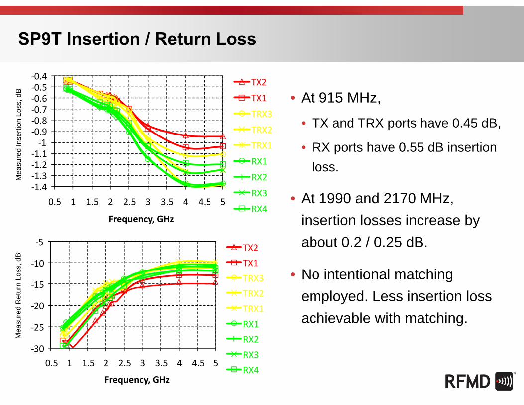
• At 915 MHz,
• TX and TRX ports have 0.45 dB,
• RX ports have 0.55 dB insertion loss.
• At 1990 and 2170 MHz, insertion losses increase by about 0.2 / 0.25 dB.
• No intentional matching employed. Less insertion loss achievable with matching.
‐1.4‐1.3‐1.2‐1.1‐1
‐0.9‐0.8‐0.7‐0.6‐0.5‐0.4
0.5 1 1.5 2 2.5 3 3.5 4 4.5 5
Frequency, GHz
TX2TX1TRX3TRX2TRX1RX1RX2RX3RX4
‐30
‐25
‐20
‐15
‐10
‐5
0.5 1 1.5 2 2.5 3 3.5 4 4.5 5
Frequency, GHz
TX2TX1TRX3TRX2TRX1RX1RX2RX3RX4
Mea
sure
d In
serti
on L
oss,
dB
Mea
sure
d R
etur
n Lo
ss, d
B
SP9T Insertion / Return Loss
dB 1990 MHz915 MHz 2170 MHz
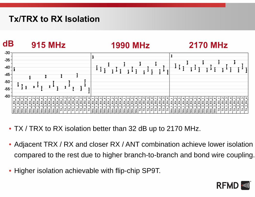
• TX / TRX to RX isolation better than 32 dB up to 2170 MHz.
• Adjacent TRX / RX and closer RX / ANT combination achieve lower isolation compared to the rest due to higher branch-to-branch and bond wire coupling.
• Higher isolation achievable with flip-chip SP9T.
Tx/TRX to RX Isolation
1990 MHz915 MHz 2170 MHzdB
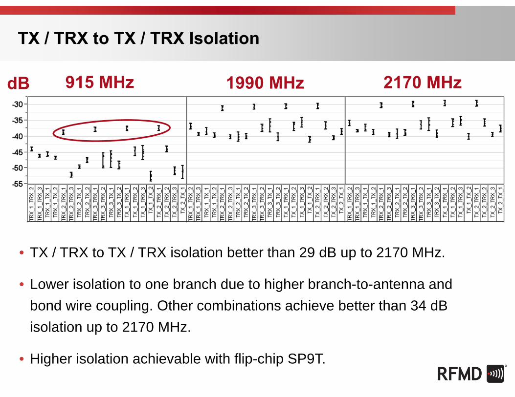
• TX / TRX to TX / TRX isolation better than 29 dB up to 2170 MHz.
• Lower isolation to one branch due to higher branch-to-antenna and bond wire coupling. Other combinations achieve better than 34 dB isolation up to 2170 MHz.
• Higher isolation achievable with flip-chip SP9T.
TX / TRX to TX / TRX Isolation
1990 MHz915 MHz 2170 MHzdB
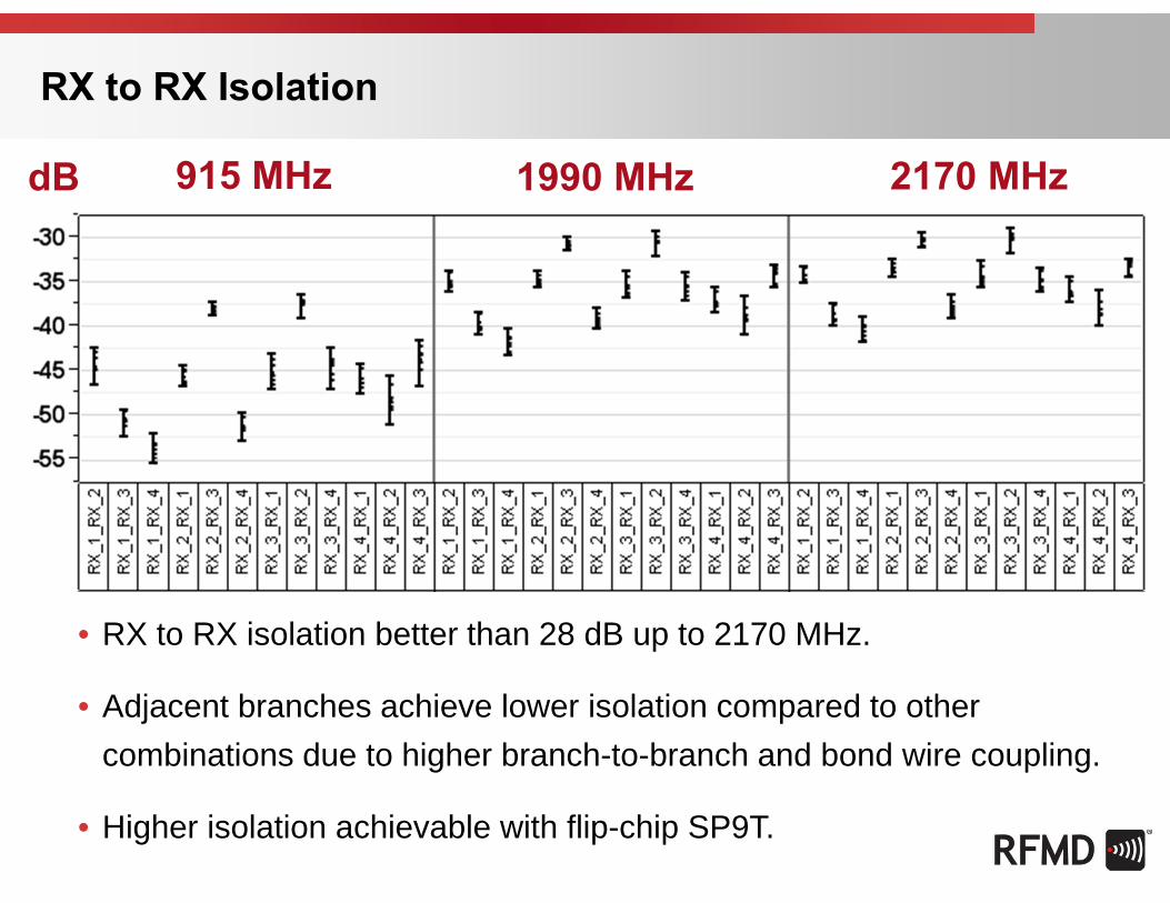
• RX to RX isolation better than 28 dB up to 2170 MHz.
• Adjacent branches achieve lower isolation compared to other combinations due to higher branch-to-branch and bond wire coupling.
• Higher isolation achievable with flip-chip SP9T.
RX to RX Isolation
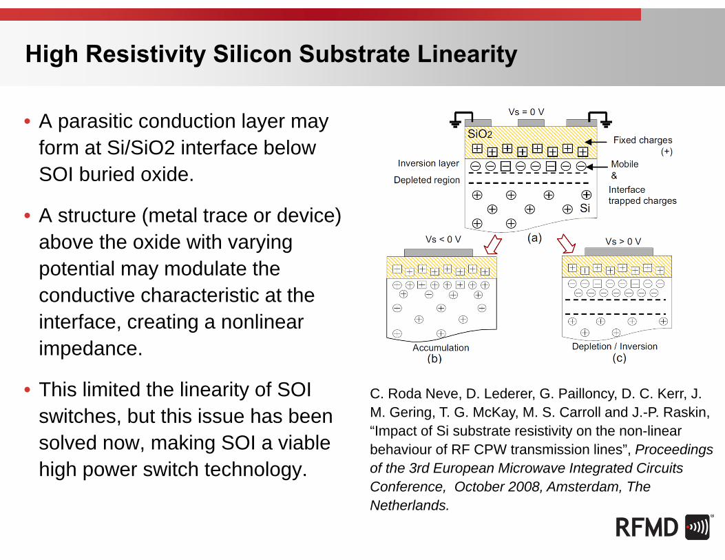
• A parasitic conduction layer may form at Si/SiO2 interface below SOI buried oxide.
• A structure (metal trace or device) above the oxide with varying potential may modulate the conductive characteristic at the interface, creating a nonlinear impedance.
• This limited the linearity of SOI switches, but this issue has been solved now, making SOI a viable high power switch technology.
C. Roda Neve, D. Lederer, G. Pailloncy, D. C. Kerr, J. M. Gering, T. G. McKay, M. S. Carroll and J.-P. Raskin, “Impact of Si substrate resistivity on the non-linear behaviour of RF CPW transmission lines”, Proceedings of the 3rd European Microwave Integrated Circuits Conference, October 2008, Amsterdam, The Netherlands.
High Resistivity Silicon Substrate Linearity
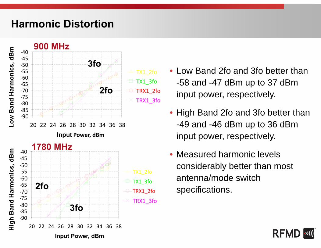
900 MHz
1780 MHz
• Low Band 2fo and 3fo better than -58 and -47 dBm up to 37 dBm input power, respectively.
• High Band 2fo and 3fo better than -49 and -46 dBm up to 36 dBm input power, respectively.
• Measured harmonic levels considerably better than most antenna/mode switch specifications.
2fo
3fo
2fo
‐90‐85‐80‐75‐70‐65‐60‐55‐50‐45‐40
20 22 24 26 28 30 32 34 36 38
Input Power, dBm
TX1_2foTX1_3foTRX1_2foTRX1_3fo
‐90‐85‐80‐75‐70‐65‐60‐55‐50‐45‐40
20 22 24 26 28 30 32 34 36 38
Input Power, dBm
TX1_2fo
TX1_3fo
TRX1_2fo
TRX1_3fo
Low
Ban
d H
arm
onic
s, d
Bm
3fo
2fo
Hig
h B
and
Har
mon
ics,
dB
m
Harmonic Distortion

• SP9T high power branches tested for breakdown.
• No measurable degradation in insertion loss and harmonics observed up to 37.5 dBm with VSWR = 3:1 at LB.
VSWR=3:1
VSWR=3:1
VSWR=3:1
SP9T Power Handling
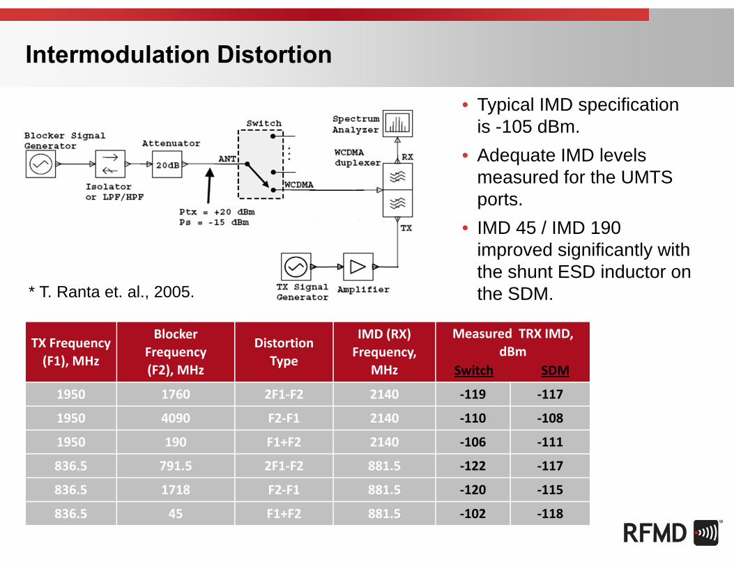
* T. Ranta et. al., 2005.
TX Frequency (F1), MHz
Blocker Frequency (F2), MHz
Distortion Type
IMD (RX) Frequency,
MHz
Measured TRX IMD, dBm
Switch SDM
1950 1760 2F1‐F2 2140 ‐119 ‐117
1950 4090 F2‐F1 2140 ‐110 ‐108
1950 190 F1+F2 2140 ‐106 ‐111
836.5 791.5 2F1‐F2 881.5 ‐122 ‐117
836.5 1718 F2‐F1 881.5 ‐120 ‐115
836.5 45 F1+F2 881.5 ‐102 ‐118
• Typical IMD specification is -105 dBm.
• Adequate IMD levels measured for the UMTS ports.
• IMD 45 / IMD 190 improved significantly with the shunt ESD inductor on the SDM.
Intermodulation Distortion

RBW=30 kHz
VBW=500 kHz
‐150‐145‐140‐135‐130‐125‐120‐115‐110‐105‐100
0.8
0.82
0.84
0.86
0.88 0.9
0.92
0.94
0.96
0.98 1
Spurious Level, dBm
Frequency, GHz
Offset -17 dB0
-150
-145
-140
-135
-130
-125
-120
-115
-110
-105
-100
SWP 50 of 50
• Measured RX mode spurious emissions better than -123 dBm.
• Measured RX band noise better than -97 dBm with fTX = 915 MHz and PTX = 35 dBm.
Spurious Emissions

• 3G / 4G smart handsets will dominate the market in the next few years, presenting a great opportunity for front-end suppliers.
• High resistivity SOI enables FET stacking, allowing the design of high power antenna / mode switches.
• Low RON*COFF product results in competitive switch insertion loss and isolation performance.
• High resistivity SOI substrate linearity issues solved, enabling the design of high throw count SOI antenna switches with excellent harmonic and intermodulation distortion performance.
• Adequate levels of TX and RX mode spurious emissions measured.
• 2000 V Human Body Model (HBM) ESD tolerance achieved on the RF ports (no blocking capacitors used on ports).
Conclusion

Do You Have Any Questions?


![14 RFDZ MW.ppt [Kompatibilitätsmodus] · Multimode Cavity Monomode (Single Mode) Cavity (rectangular waveguide) antenna magnetron mode stirrer sample sample wave guide magnetron](https://cdn.vdocuments.mx/doc/165x107/5b7be53e7f8b9a4c4a8d8ca8/14-rfdz-mwppt-kompatibilitaetsmodus-multimode-cavity-monomode-single-mode.jpg)


