
Analysis and Experiment on Harmonic CurrentDistortion in Wireless Power Transfer System
Using a Diode Rectifier
Katsuhiro Hata, Takehiro Imura, and Yoichi HoriThe University of Tokyo,
5–1–5, Kashiwanoha, Kashiwa, Chiba, 277–8561, JapanPhone: +81-4-7136-3881, Fax: 81-4-7136-3881
Email: [email protected], [email protected], [email protected]
Abstract—Wireless power transfer (WPT) via magnetic reso-nance coupling provides highly efficient mid-range transmission.Its transmitting power can be controlled using a diode rectifierand a DC-DC converter on the secondary side. Previous researchreplaces the load and the rectifier circuit with an equivalentload resistance or a fundamental harmonic sine wave voltagesource to analyze the charging power of WPT. In such a casehowever, the effect caused by the rectifier circuit becomes unclearbecause the harmonic components are neglected. As a result,the theoretical charging power and its true value have an errordue to the harmonic current distortion. In this paper, a novelWPT circuit model is proposed for the analysis of the harmoniccurrent distortion on the secondary side. The proposed modeluses the secondary voltage as the input variable of transferfunctions and makes clear the effect caused by the rectifier circuit.Experiments demonstrate that the harmonic current distortion isincreased with the increase in the secondary voltage. These resultsaccord with the analysis using the proposed model and verify theeffectiveness of the proposed model.
Keywords—Wireless power transfer, Magnetic resonance cou-pling, Diode rectifier, Harmonic current distortion.
I. INTRODUCTION
Electric vehicles (EVs) have environmental advantages andthe capacity for advanced motion control due to the fastresponse time of their electric motors [1]. However, EVs needto be charged frequently due to their limited mileage percharge. Charging operations should be simplified to reduce theburden on the user.
Wireless power transfer (WPT) can mitigate complicatedcharging operations and apply dynamic charging to EVs in mo-tion [2], [3]. WPT via magnetic resonance coupling provideshighly efficient mid-range transmission and it has robustness tomisalignment between a transmitter and a receiver [4], [5]. Itstransmitting efficiency and its charging power are determinednot only by the parameters of the transmitter and the receiverbut also by the load [6]. The load condition can be controlledusing a diode rectifier and a DC-DC converter on the secondaryside [7], [8]. As a result, the transmitting efficiency can bemaximized [9], [10] or the charging power can be controlledon the secondary side [11]–[13].
Many papers on the modeling of the WPT circuit use anequivalent load resistance, which includes the load and therectifier circuit [14]–[16]. A previous study [17] has proposed
RL
V1
Power source Load
V2
I1
I2
C1
C2
R2
L2
R1
L1
Lm
Transmitter and Receiver
(a) Equivalent circuit of magnetic resonant coupling.
RLV
1
Power source Load
V2
I1
I2
C1
C2R
2R1 L
1-L
m
Lm
Transmitter and receiver
L2-L
m
(b) T–type equivalent circuit.
Fig. 1. Equivalent circuit of the wireless power transfer system.
a fundamental mode equivalent circuit, which replaces theload and the rectifier circuit with a fundamental harmonicsine wave voltage source. Furthermore, the WPT circuit modelconsidering the discontinuous mode of the diode rectifierhas been represented [18], [19]. However, the actual load isreplaced by an equivalent load resistance or a fundamentalharmonic sine wave voltage source. As a result, the effectscaused by the diode rectifier cannot be made clear because theharmonic components are neglected. This causes an error inthe theoretical charging power of WPT.
This paper proposes a novel WPT circuit model, whichis expressed by multi-input, multi-output (MIMO) transferfunctions using the secondary voltage as the input variable.The proposed model can analyze the harmonic current dis-tortion caused by the rectifier circuit because the load is notapproximated by any elements. Experiments show that thecharging power control on the secondary side using the dioderectifier has the potential for causing the harmonic currentdistortion. This result is analyzed using the proposed modeland the effectiveness of the proposed model is verified.

0
0.5
1
1.5
2
2.5
0
0.2
0.4
0.6
0.8
1
1 10 100 1000 10000 100000
Ch
agin
g p
ow
erP
[kW
]
Tra
nsm
itti
ng e
ffic
ien
cy η
Load resistance RL [Ω]
η
P
Fig. 2. Load resistance vs. transmitting efficiency and charging power.
II. WIRELESS POWER TRANSFER VIA MAGNETICRESONANCE COUPLING
A. Characteristics at resonance frequency
A series-series circuit topology is used for the wirelesspower transfer circuit and its equivalent circuit is shown inFig. 1 [20]. The transmitter and the receiver are characterizedby the inductances L1, L2, the series-resonance capacitors C1,C2, and the internal resistances R1, R2, respectively. Lm is themutual inductance between the transmitter and the receiver.V1 is the RMS voltage of a power source and its angularfrequency is expressed as ω0. The transmitter and the receiverare designed to satisfy the following equation.
ω0 =1√L1C1
=1√L2C2
(1)
When the load resistance is RL, the voltage ratio AV
and the current ratio AI between the secondary-side and theprimary-side are expressed as follows:
AV =V2
V1= j
ω0LmRL
R1R2 +R1RL + (ω0Lm)2(2)
AI =I2I1
= jω0Lm
R2 +RL(3)
where V2, I1, and I2 are the RMS values of the secondaryvoltage, the primary current, and the secondary current, re-spectively. Then, the transmitting efficiency η is expressed asfollows:
η =(ω0Lm)2RL
(R2 +RL)R1R2 +R1RL + (ω0Lm)2(4)
and the charging power P is described as follows:
P =(ω0Lm)2RL
R1R2 +R1RL + (ω0Lm)22V1
2. (5)
Fig. 2 shows the load resistance RL versus the transmittingefficiency η and the charging power P . The parameters of thetransmitter and the receiver, which are used in this work, aregiven in TABLE I. The amplitude of V1 is equal to 100 V. ηis maximized if RL is given as follows:
RLηmax =
√R2
(ω0Lm)2
R1+R2
. (6)
0
0.5
1
1.5
2
2.5
0
0.2
0.4
0.6
0.8
1
1 10 100 1000 10000
Ch
argin
g p
ow
er P
[kW
]
Tra
nsm
itti
ng e
ffic
ien
cy η
Secondary voltage V2 [V]
η
P
Fig. 3. Secondary voltage vs. transmitting efficiency and charging power.
TABLE I. PARAMETERS OF TRANSMITTER AND RECEIVER.
Primary side Secondary side
Resistance R1, R2 1.14 Ω 1.19 Ω
Inductance L1, L2 637.9 µH 638.4 µHCapacitance C1, C2 4002 pF 3996 pFResonant frequency f1, f2 99.6 kHz 99.6 kHz
Mutual inductance Lm 81.5 µH (gap: 200 mm)
Outer diameter 448 mm
Number of turns 56 turns
P is maximized if RL is expressed as follows:
RLPmax =(ω0Lm)2
R1+R2. (7)
B. Charging power control on the secondary side
The load resistance RL is determined by the amplitudeof the secondary voltage V2, which can be controlled by theDC-DC converter on the secondary side. Fig. 3 shows thesecondary voltage V2 versus the transmitting efficiency η andthe charging power P . If the maximum efficiency is achieved,V2 satisfies the following equation [9].
V2ηmax =
√R2
R1
ω0Lm√R1R2 + (ω0Lm)2 +
√R1R2
V1 (8)
Charging power control can be achieved by secondaryvoltage control [12], [13]. However, it is effective only if V2
is controlled below the maximum secondary voltage V2max,which is expressed as follows:
V2max =ω0Lm
R1V1. (9)
Then, the equivalent load resistance RL goes to infinity andthe voltage ratio AV becomes saturated [6]. The maximumpower is obtained when V2 is given as follows:
V2Pmax =ω0Lm
2R1V1 =
V2max
2. (10)
For efficient transmission, it is important to define theoperating range of V2 to be below V2Pmax. As a result, the

Receiver
Transmitter
DC-DC
converter
Rectifier
M
Battery
Power source
Motor drive
Electric vehicle
Ground facility
Fig. 4. System configuration of wireless charging for electric vehicle.
Idc
Vdc C
L r
E
IL
LmC1 C2R2
L2
R1
L1V
1
Power source Transmitter and receiver Rectifier DC-DC converter Battery
V2
I1 I2
VS
P
d
Fig. 5. Circuit diagram of the wireless charging system.
reference voltage V2∗, which obtains the desired power P ∗, is
given as follows [13]:
V2∗ =
(ω0LmV1
2R1
)−√(
ω0LmV1
2R1
)2
− R1R2 + (ω0Lm)2P ∗
R1. (11)
C. Effect of the diode rectifier
Fig. 4 shows a system configuration of wireless chargingfor an EV. Assuming that the voltage control of the DC-DCconverter is designed properly, the charging power controlcan be achieved. The circuit diagram of the wireless chargingsystem is shown in Fig. 5. In this paper, the motor drive systemis neglected as this is a fundamental study.
The secondary voltage is generated by the diode rectifier.If the absolute value of the secondary voltage exceeds theamplitude of the DC link voltage Vdc, the rectifier is conductedand the absolute value of the secondary voltage becomes thesame amplitude as Vdc, where the forward voltage of the diodeis ignored. Furthermore, if the amplitude of Vdc is much lowerthan the amplitude of V2max, the secondary voltage can beassumed to be a square wave.
On the other hand, in the case where the absolute value ofthe secondary voltage cannot be larger than the amplitude ofVdc, the secondary current cannot flow through the rectifier.Therefore, the secondary current includes the discontinuousstate and could not be strictly approximated by the sine wave.
III. MODELING OF THE WIRELESS POWER TRANSFERCIRCUIT
A. Conventional model using the equivalent load resistance
Previous research [16] has proposed a transfer functionmodel of the WPT circuit using the equivalent load resistanceRL. Its block diagram is shown in Fig. 6. Yc1(s) and Yc2(s)are transfer functions from the primary voltage V1(s) to theprimary current I1(s) and the secondary current I2(s). Forthe charging power control on the secondary side, this paperfocuses on Yc2(s). This is given as follows:
Yc2(s) =I2(s)
V1(s)=
bc3s3
s4 + ac3s3 + ac2s2 + ac1s+ ac0(12)
where each coefficient is defined as follows:
ac3 =R1L2 + (R2 +RL)L1
L1L2 − Lm2 (13)
ac2 =R1(R2 +RL) + (L1/C2) + (L2/C1)
L1L2 − Lm2 (14)
ac1 =(R1/C2) + (R2 +RL)/C1
L1L2 − Lm2 (15)
ac0 =1
C1C2(L1L2 − Lm2)
(16)
bc3 =−Lm
L1L2 − Lm2 . (17)
The bode diagram of Yc2(s) is shown in Fig. 7. In thismodel, it is difficult to analyze the harmonic current distor-

Yc2 (s)
Yc1 (s)
RL = f (V2 (s))
V1 (s)
I2 (s)
I1 (s)
Fig. 6. Block diagram of the conventional model.
104
105
106
-100
-80
-60
-40
-20
0
Mag
nit
ud
e [d
B]
104
105
106
-90
0
90
180
270
Frequency [Hz]
Ph
ase
[deg
]
RL=10 Ω
RL=100 Ω
RL=10 Ω
RL=100 Ω
Fig. 7. Bode diagram of the conventional transfer function Yc2.
tion because the bode diagram is changed by RL, which iscontrolled to achieve the desired charging power.
B. Proposed model using the secondary voltage as an inputvariable
This paper proposes a transfer function model of theWPT circuit using the secondary voltage V2(s) as the inputvariable instead of using the equivalent load resistance RL.The dynamics of the T-type equivalent circuit in Fig. 1 can beexpressed as follows:[
I1(s)
I2(s)
]=
[Y11(s) Y12(s)
Y21(s) Y22(s)
] [V1(s)
V2(s)
](18)
where Y11(s), Y12(s), Y21(s), and Y22(s) are transfer functionsfrom V1(s) and V2(s) to I1(s) and I2(s). The block diagramof the proposed model is shown in Fig. 8. Then, I2(s) isexpressed as follows:
I2(s) = Y21(s)V1(s) + Y22(s)V2(s). (19)
From the circuit equations, Y21(s) and Y22(s) are described asfollows:
Y21(s) =I2(s)
V1(s)=
b3s3
s4 + a3s3 + a2s2 + a1s+ a0(20)
Y22(s) =I2(s)
V2(s)=
d3s3 + d2s
2 + d1s
s4 + a3s3 + a2s2 + a1s+ a0(21)
Y21 (s)
V1 (s)
++
Y22 (s)
Y12 (s)
Y11 (s)
V2 (s) I2 (s)
I1 (s)+
+
Fig. 8. Block diagram of the proposed model.
104
105
106
-100
-80
-60
-40
-20
0
Mag
nit
ud
e [d
B]
Y21
Y22
104
105
106
-90
0
90
180
270
Frequency [Hz]
Ph
ase
[deg
]
Y21
Y22
Fig. 9. Bode diagram of the proposed transfer functions Y21 and Y22.
where each coefficient is defined as follows:
a3 =R1L2 +R2L1
L1L2 − Lm2 (22)
a2 =R1R2 + (L1/C2) + (L2/C1)
L1L2 − Lm2 (23)
a1 =(R1/C2) + (R2/C1)
L1L2 − Lm2 (24)
a0 =1
C1C2(L1L2 − Lm2)
(25)
b3 =−Lm
L1L2 − Lm2 (26)
d3 =L1
L1L2 − Lm2 (27)
d2 =R1
L1L2 − Lm2 (28)
d1 =1
C1(L1L2 − Lm2). (29)
The bode diagram of Y21(s) and Y22(s) is shown in Fig. 9.Since two out of three zeros of Y22(s) exist at the resonancefrequency, the gain of Y22(s) is decreased at the resonancefrequency. As a result, the harmonic components of V2(s) arenot suppressed and have an effect on the harmonic distortionof I2(s).

V1
Power source
V2
I1
I2
C1
C2R
2R1 L
1-Lm
Lm
Transmitter and receiver
L2-Lm
Vdc
Rectifier
Fig. 10. Experimental circuit of the wireless power transfer system.
(a) Transmitter and receiver.
(b) Rectifier.
Function generator
Power analyzer
Electronic load
High speed bipolar amplifier
(c) Power source, load, and analyzer.
Fig. 11. Experimental equipment.
IV. EXPERIMENTS
A. Experimental setup
The wireless power transfer system, which is indicatedin Fig. 10, was built and tested. In order to eliminate theharmonic components caused by the primary voltage, a sinewave voltage source was used. Therefore, the harmonic currentdistortion is caused by only the diode rectifier, which generatesthe secondary voltage. In addition, the DC-DC converter wasreplaced by an electronic load, which simulated a constantvoltage load.
The experimental equipment is shown in Fig. 11.The power source was composed of a function generator(AFG3021B, Tektronix) and a high speed bipolar amplifier(HSA4014, NF Corporation). The amplitude of the primaryvoltage V1 was tuned to 10 V and the operating frequency wasset to 99.6 kHz. The diode rectifier consisted of Schottky bar-rier diodes (SB560, Fairchild semiconductor). The amplitudeof the DC link voltage Vdc was regulated by the electronic load(PLZ1004W, KIKUSUI). Waveforms of the secondary voltageand the secondary current were measured by a mixed signaloscilloscope (MSO3034, Tektronix) and their harmonics wereanalyzed by a power analyzer (PPA5530, Newtons4th Ltd.).
-0.4
-0.3
-0.2
-0.1
0
0.1
0.2
0.3
0.4
-20
-15
-10
-5
0
5
10
15
20
0 5 10 15 20
Sec
on
dar
y c
urr
ent
i 2[A
]
Sec
on
dar
y v
olt
age
v2
[V]
Time [µs]
v2
i2
(a) Vdc = 10 V.
-0.25
-0.2
-0.15
-0.1
-0.05
0
0.05
0.1
0.15
0.2
0.25
-100
-80
-60
-40
-20
0
20
40
60
80
100
0 5 10 15 20
Sec
on
dar
y c
urr
ent
i 2[A
]
Sec
on
dar
y v
olt
age
v2
[V]
Time [µs]
v2
i2
(b) Vdc = 50 V.
Fig. 12. Measured waveforms of the secondary voltage and the secondarycurrent.
B. Experimental results
The measured waveforms are shown in Fig. 12. Whenthe amplitude of Vdc is equal to 10 V, the waveform of thesecondary current is close to a sine wave. On the other hand,when the amplitude of Vdc is set to 50 V, it is seen thatthe secondary current is distorted slightly at the zero-crossingbecause of the discontinuous state. Additionally, the secondaryvoltage and the secondary current are not in phase. This iscaused by the harmonic components of the secondary voltage.
The total harmonic distortion (THD) of the secondarycurrent is indicated in Fig. 13. As the amplitude of Vdc isincreased, the secondary current has a higher proportion of theharmonic components. This result can be analyzed using theproposed model. When the amplitude of Vdc is larger than theamplitude of V1, the secondary current is dominantly affectedby Y22(s) due to eq. (19). Since Y22(s) cannot suppress theharmonic components of the secondary voltage, the harmoniccomponents of the secondary current is increased.
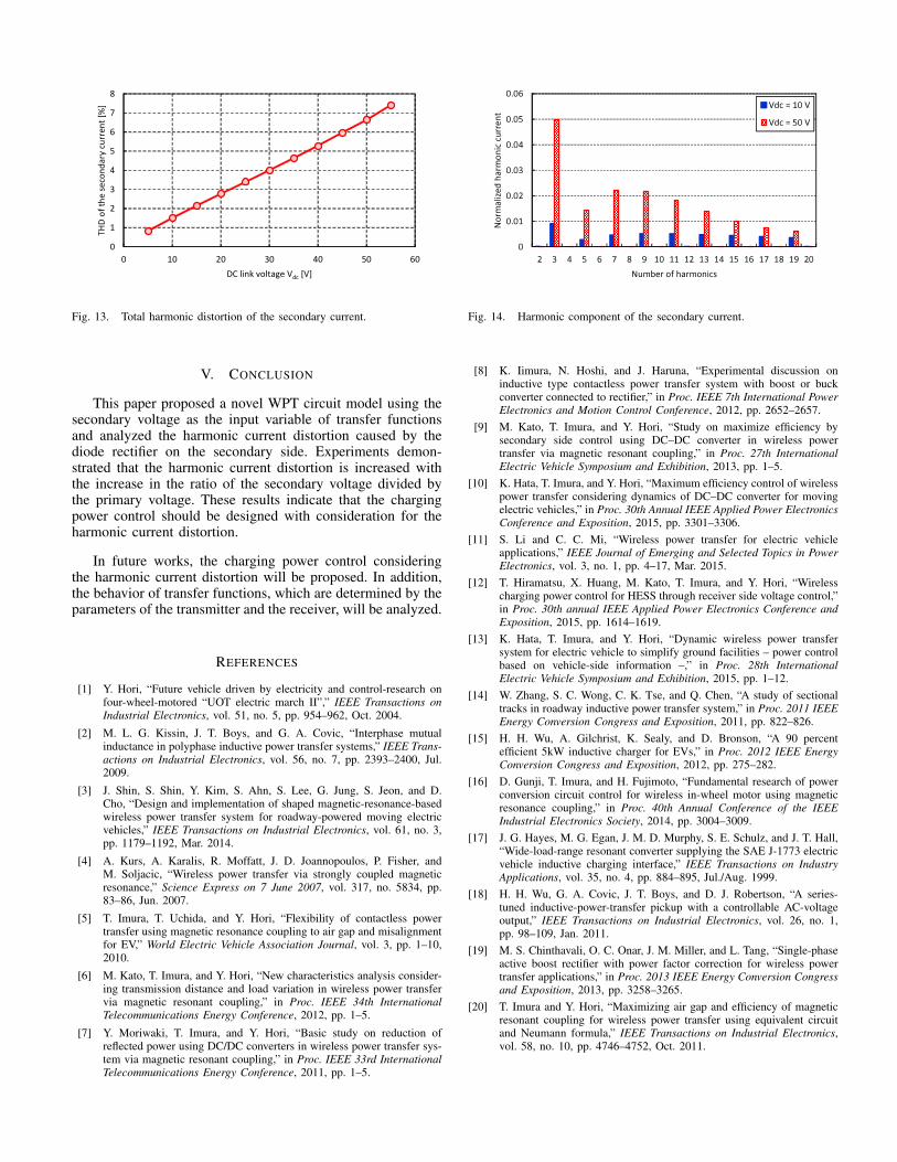
Fig. 14 shows the harmonic component of the secondarycurrent and indicates that the secondary current has odd-orderharmonics. Therefore, it is verified that the secondary current isdistorted by the harmonic components of the secondary voltagedue to the diode rectifier.
In the case where the desired charging power is larger, theamplitude of Vdc has to be increased. Therefore, the chargingpower control should be designed considering the harmoniccurrent distortion to achieve the desired charging power.
0
1
2
3
4
5
6
7
8
0 10 20 30 40 50 60
TH
D o
f th
e s
eco
nd
ary
cu
rre
nt
[%]
DC link voltage Vdc
[V]
Fig. 13. Total harmonic distortion of the secondary current.
V. CONCLUSION
This paper proposed a novel WPT circuit model using thesecondary voltage as the input variable of transfer functionsand analyzed the harmonic current distortion caused by thediode rectifier on the secondary side. Experiments demon-strated that the harmonic current distortion is increased withthe increase in the ratio of the secondary voltage divided bythe primary voltage. These results indicate that the chargingpower control should be designed with consideration for theharmonic current distortion.
In future works, the charging power control consideringthe harmonic current distortion will be proposed. In addition,the behavior of transfer functions, which are determined by theparameters of the transmitter and the receiver, will be analyzed.
REFERENCES
[1] Y. Hori, “Future vehicle driven by electricity and control-research onfour-wheel-motored “UOT electric march II”,” IEEE Transactions onIndustrial Electronics, vol. 51, no. 5, pp. 954–962, Oct. 2004.
[2] M. L. G. Kissin, J. T. Boys, and G. A. Covic, “Interphase mutualinductance in polyphase inductive power transfer systems,” IEEE Trans-actions on Industrial Electronics, vol. 56, no. 7, pp. 2393–2400, Jul.2009.
[3] J. Shin, S. Shin, Y. Kim, S. Ahn, S. Lee, G. Jung, S. Jeon, and D.Cho, “Design and implementation of shaped magnetic-resonance-basedwireless power transfer system for roadway-powered moving electricvehicles,” IEEE Transactions on Industrial Electronics, vol. 61, no. 3,pp. 1179–1192, Mar. 2014.
[4] A. Kurs, A. Karalis, R. Moffatt, J. D. Joannopoulos, P. Fisher, andM. Soljacic, “Wireless power transfer via strongly coupled magneticresonance,” Science Express on 7 June 2007, vol. 317, no. 5834, pp.83–86, Jun. 2007.
[5] T. Imura, T. Uchida, and Y. Hori, “Flexibility of contactless powertransfer using magnetic resonance coupling to air gap and misalignmentfor EV,” World Electric Vehicle Association Journal, vol. 3, pp. 1–10,2010.
[6] M. Kato, T. Imura, and Y. Hori, “New characteristics analysis consider-ing transmission distance and load variation in wireless power transfervia magnetic resonant coupling,” in Proc. IEEE 34th InternationalTelecommunications Energy Conference, 2012, pp. 1–5.
[7] Y. Moriwaki, T. Imura, and Y. Hori, “Basic study on reduction ofreflected power using DC/DC converters in wireless power transfer sys-tem via magnetic resonant coupling,” in Proc. IEEE 33rd InternationalTelecommunications Energy Conference, 2011, pp. 1–5.
0
0.01
0.02
0.03
0.04
0.05
0.06
2 3 4 5 6 7 8 9 10 11 12 13 14 15 16 17 18 19 20
No
rm
alize
d h
arm
on
ic c
urre
nt
Number of harmonics
Vdc = 10 V
Vdc = 50 V
Fig. 14. Harmonic component of the secondary current.
[8] K. Iimura, N. Hoshi, and J. Haruna, “Experimental discussion oninductive type contactless power transfer system with boost or buckconverter connected to rectifier,” in Proc. IEEE 7th International PowerElectronics and Motion Control Conference, 2012, pp. 2652–2657.
[9] M. Kato, T. Imura, and Y. Hori, “Study on maximize efficiency bysecondary side control using DC–DC converter in wireless powertransfer via magnetic resonant coupling,” in Proc. 27th InternationalElectric Vehicle Symposium and Exhibition, 2013, pp. 1–5.
[10] K. Hata, T. Imura, and Y. Hori, “Maximum efficiency control of wirelesspower transfer considering dynamics of DC–DC converter for movingelectric vehicles,” in Proc. 30th Annual IEEE Applied Power ElectronicsConference and Exposition, 2015, pp. 3301–3306.
[11] S. Li and C. C. Mi, “Wireless power transfer for electric vehicleapplications,” IEEE Journal of Emerging and Selected Topics in PowerElectronics, vol. 3, no. 1, pp. 4–17, Mar. 2015.
[12] T. Hiramatsu, X. Huang, M. Kato, T. Imura, and Y. Hori, “Wirelesscharging power control for HESS through receiver side voltage control,”in Proc. 30th annual IEEE Applied Power Electronics Conference andExposition, 2015, pp. 1614–1619.
[13] K. Hata, T. Imura, and Y. Hori, “Dynamic wireless power transfersystem for electric vehicle to simplify ground facilities – power controlbased on vehicle-side information –,” in Proc. 28th InternationalElectric Vehicle Symposium and Exhibition, 2015, pp. 1–12.
[14] W. Zhang, S. C. Wong, C. K. Tse, and Q. Chen, “A study of sectionaltracks in roadway inductive power transfer system,” in Proc. 2011 IEEEEnergy Conversion Congress and Exposition, 2011, pp. 822–826.
[15] H. H. Wu, A. Gilchrist, K. Sealy, and D. Bronson, “A 90 percentefficient 5kW inductive charger for EVs,” in Proc. 2012 IEEE EnergyConversion Congress and Exposition, 2012, pp. 275–282.
[16] D. Gunji, T. Imura, and H. Fujimoto, “Fundamental research of powerconversion circuit control for wireless in-wheel motor using magneticresonance coupling,” in Proc. 40th Annual Conference of the IEEEIndustrial Electronics Society, 2014, pp. 3004–3009.
[17] J. G. Hayes, M. G. Egan, J. M. D. Murphy, S. E. Schulz, and J. T. Hall,“Wide-load-range resonant converter supplying the SAE J-1773 electricvehicle inductive charging interface,” IEEE Transactions on IndustryApplications, vol. 35, no. 4, pp. 884–895, Jul./Aug. 1999.
[18] H. H. Wu, G. A. Covic, J. T. Boys, and D. J. Robertson, “A series-tuned inductive-power-transfer pickup with a controllable AC-voltageoutput,” IEEE Transactions on Industrial Electronics, vol. 26, no. 1,pp. 98–109, Jan. 2011.
[19] M. S. Chinthavali, O. C. Onar, J. M. Miller, and L. Tang, “Single-phaseactive boost rectifier with power factor correction for wireless powertransfer applications,” in Proc. 2013 IEEE Energy Conversion Congressand Exposition, 2013, pp. 3258–3265.
[20] T. Imura and Y. Hori, “Maximizing air gap and efficiency of magneticresonant coupling for wireless power transfer using equivalent circuitand Neumann formula,” IEEE Transactions on Industrial Electronics,vol. 58, no. 10, pp. 4746–4752, Oct. 2011.


