SN54ALS138A, SN54AS138, SN74ALS138A, SN74AS1383-LINE TO 8-LINE DECODERS/DEMULTIPLEXERS
SDAS055E – APRIL 1982 – REVISED JULY 1996
1POST OFFICE BOX 655303 • DALLAS, TEXAS 75265
Designed Specifically for High-SpeedMemory Decoders and Data TransmissionSystems
Incorporate Three Enable Inputs to SimplifyCascading and/or Data Reception
Package Options Include PlasticSmall-Outline (D) Packages, Ceramic ChipCarriers (FK), and Standard Plastic (N) andCeramic (J) 300-mil DIPs
description
The ′ALS138A and ′AS138 are 3-line to 8-linedecoders/demultiplexers designed for high-performance memory-decoding or data-routingapplications requiring very short propagationdelay times. In high-performance systems, thesedevices can be used to minimize the effects ofsystem decoding. When employed withhigh-speed memories with a fast enable circuit,the delay times of the decoder and the enable timeof the memory are usually less than the typicalaccess time of the memory. The effective systemdelay introduced by the Schottky-clamped systemdecoder is negligible.
The conditions at the binary-select (A, B, and C)inputs and the three enable (G1, G2A, and G2B)inputs select one of eight output lines. Twoactive-low and one active-high enable inputsreduce the need for external gates or inverters when expanding. A 24-line decoder can be implemented withoutexternal inverters and a 32-line decoder requires only one inverter. An enable input can be used as a data inputfor demultiplexing applications.
The SN54ALS138A and SN54AS138 are characterized for operation over the full military temperature rangeof –55°C to 125°C. The SN74ALS138A and SN74AS138 are characterized for operation from 0°C to 70°C.
Copyright 1996, Texas Instruments IncorporatedPRODUCTION DATA information is current as of publication date.Products conform to specifications per the terms of Texas Instrumentsstandard warranty. Production processing does not necessarily includetesting of all parameters.
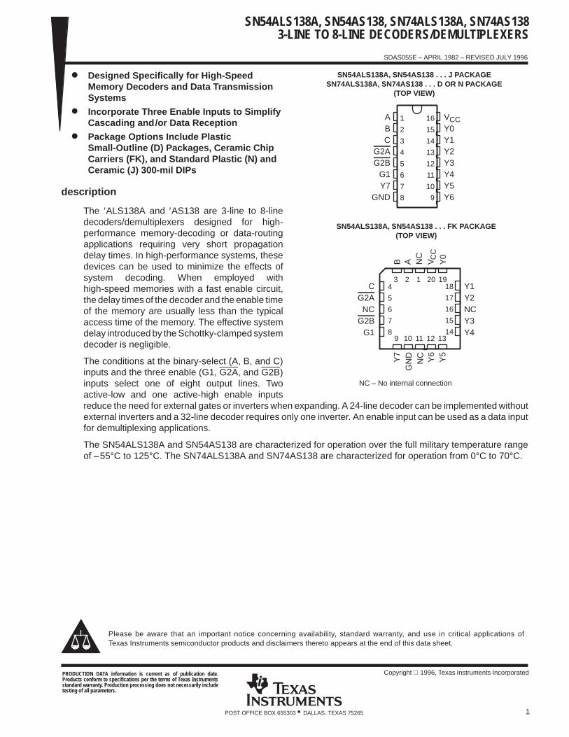
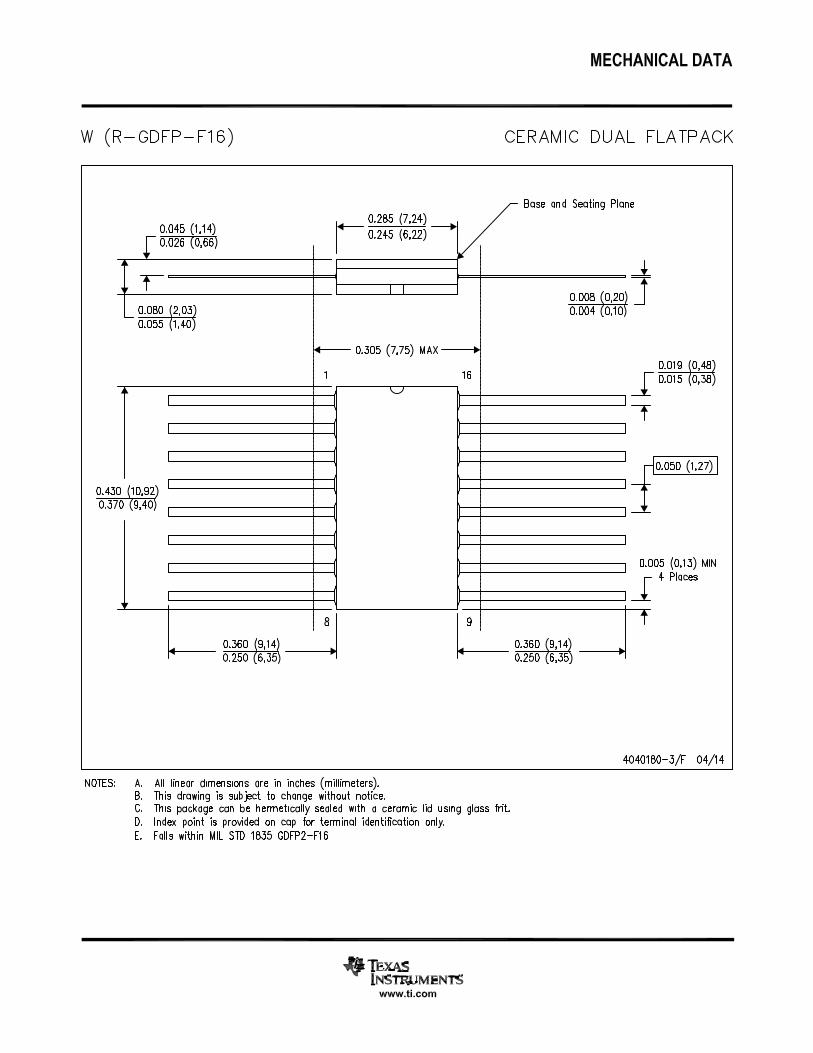
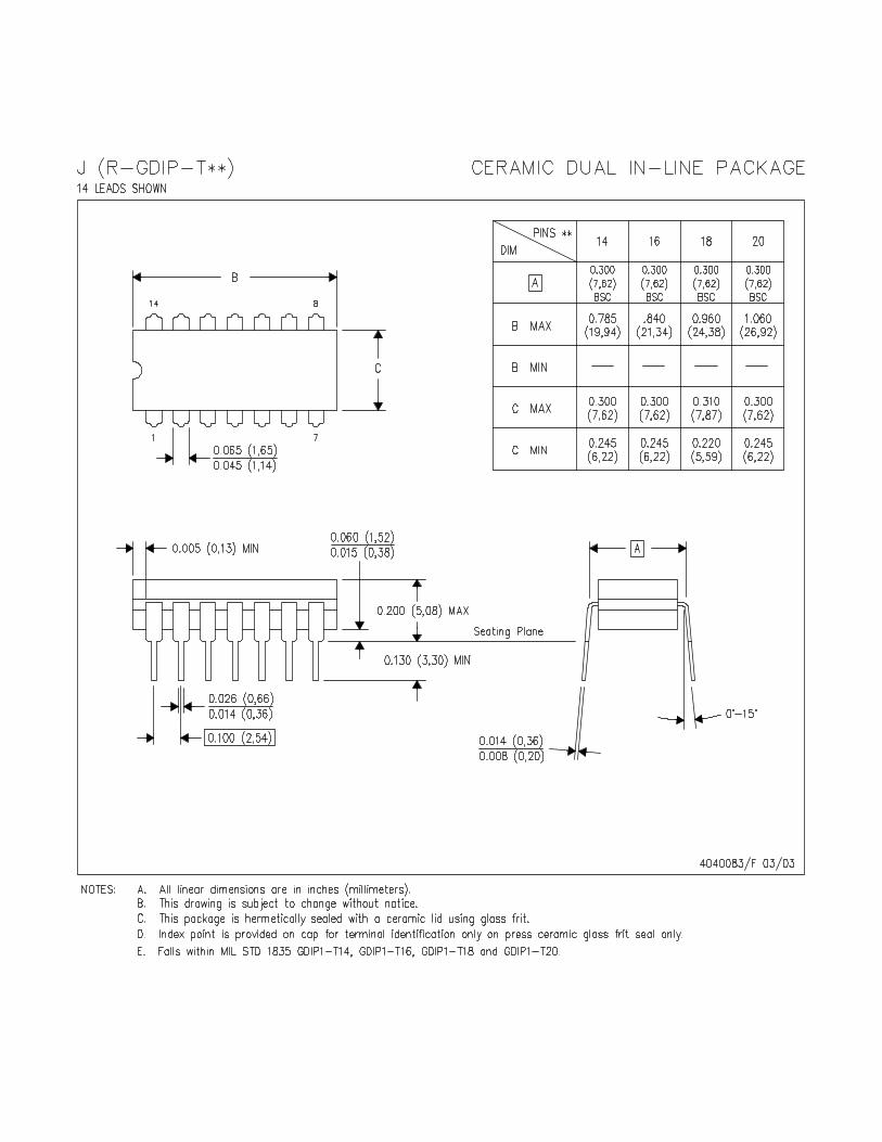
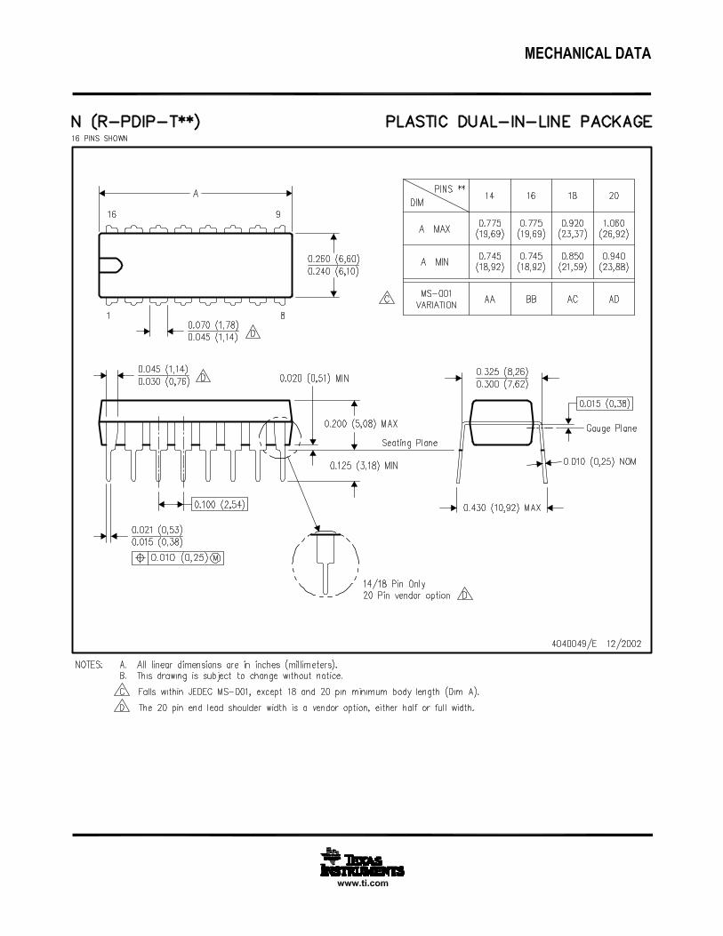
SN54ALS138A, SN54AS138 . . . J PACKAGESN74ALS138A, SN74AS138 . . . D OR N PACKAGE
(TOP VIEW)
3 2 1 20 19
9 10 11 12 13
4
5
6
7
8
18
17
16
15
14
Y1Y2NCY3Y4
CG2ANC
G2BG1
SN54ALS138A, SN54AS138 . . . FK PACKAGE(TOP VIEW)
B A NC
Y6
Y5
Y0
Y7
GN
DN
C
NC – No internal connection
VC
C
1
2
3
4
5
6
7
8
16
15
14
13
12
11
10
9
ABC
G2AG2B
G1Y7
GND
VCCY0Y1Y2Y3Y4Y5Y6
Please be aware that an important notice concerning availability, standard warranty, and use in critical applications ofTexas Instruments semiconductor products and disclaimers thereto appears at the end of this data sheet.
SN54ALS138A, SN54AS138, SN74ALS138A, SN74AS1383-LINE TO 8-LINE DECODERS/DEMULTIPLEXERS
SDAS055E – APRIL 1982 – REVISED JULY 1996
2 POST OFFICE BOX 655303 • DALLAS, TEXAS 75265
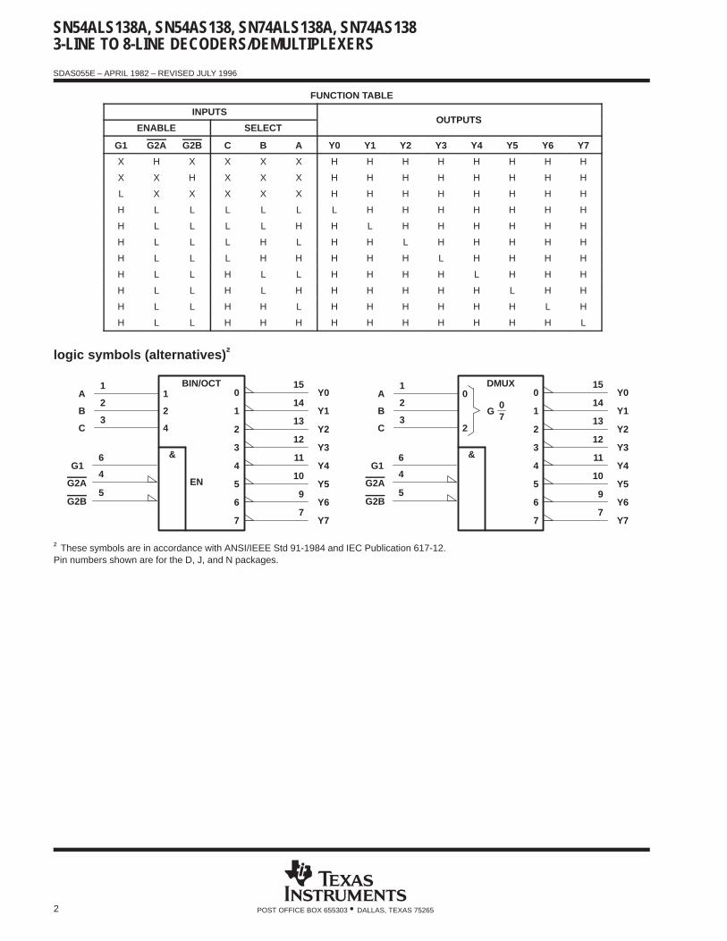
FUNCTION TABLE
INPUTSOUTPUTS
ENABLE SELECTOUTPUTS
G1 G2A G2B C B A Y0 Y1 Y2 Y3 Y4 Y5 Y6 Y7
X H X X X X H H H H H H H H
X X H X X X H H H H H H H H
L X X X X X H H H H H H H H
H L L L L L L H H H H H H H
H L L L L H H L H H H H H H
H L L L H L H H L H H H H H
H L L L H H H H H L H H H H
H L L H L L H H H H L H H H
H L L H L H H H H H H L H H
H L L H H L H H H H H H L H
H L L H H H H H H H H H H L
logic symbols (alternatives) †
BIN/OCT1
1A
22
B
43
C
4
5
6G1
Y015
0
&
EN
Y114
1
Y213
2
Y312
3
Y411
4
Y510
5
Y69
6
Y77
7
DMUX0
1A
2B
23
C
4
5
6G1
Y015
0
&
Y114
1
Y213
2
Y312
3
Y411
4
Y510
5
Y69
6
Y77
7
G 70
G2A
G2B
G2A
G2B
† These symbols are in accordance with ANSI/IEEE Std 91-1984 and IEC Publication 617-12.Pin numbers shown are for the D, J, and N packages.
SN54ALS138A, SN54AS138, SN74ALS138A, SN74AS1383-LINE TO 8-LINE DECODERS/DEMULTIPLEXERS
SDAS055E – APRIL 1982 – REVISED JULY 1996
3POST OFFICE BOX 655303 • DALLAS, TEXAS 75265
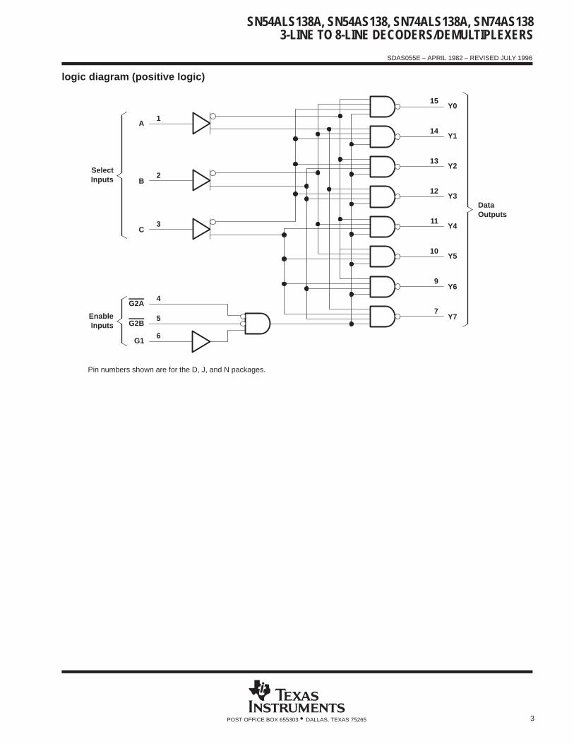
logic diagram (positive logic)
G2B
G2A
G1
C
B
A
Y7
Y6
Y5
Y4
Y3
Y2
Y1
Y0
DataOutputs
SelectInputs
EnableInputs
1
2
3
6
4
5
15
14
13
12
11
10
9
7
Pin numbers shown are for the D, J, and N packages.
SN54ALS138A, SN54AS138, SN74ALS138A, SN74AS1383-LINE TO 8-LINE DECODERS/DEMULTIPLEXERS
SDAS055E – APRIL 1982 – REVISED JULY 1996
4 POST OFFICE BOX 655303 • DALLAS, TEXAS 75265
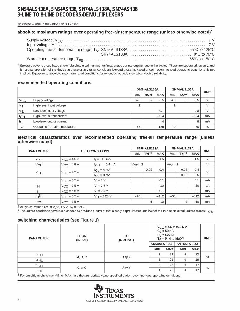
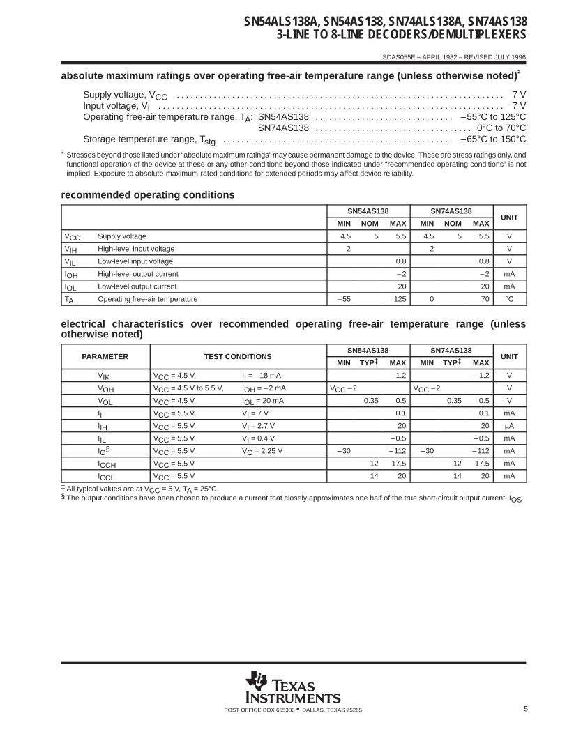
absolute maximum ratings over operating free-air temperature range (unless otherwise noted) †
Supply voltage, VCC 7 V. . . . . . . . . . . . . . . . . . . . . . . . . . . . . . . . . . . . . . . . . . . . . . . . . . . . . . . . . . . . . . . . . . . . . . . Input voltage, VI 7 V. . . . . . . . . . . . . . . . . . . . . . . . . . . . . . . . . . . . . . . . . . . . . . . . . . . . . . . . . . . . . . . . . . . . . . . . . . . Operating free-air temperature range, TA: SN54ALS138A –55°C to 125°C. . . . . . . . . . . . . . . . . . . . . . . . . . .
SN74ALS138A 0°C to 70°C. . . . . . . . . . . . . . . . . . . . . . . . . . . . . . . Storage temperature range, Tstg –65°C to 150°C. . . . . . . . . . . . . . . . . . . . . . . . . . . . . . . . . . . . . . . . . . . . . . . . . .
† Stresses beyond those listed under “absolute maximum ratings” may cause permanent damage to the device. These are stress ratings only, andfunctional operation of the device at these or any other conditions beyond those indicated under “recommended operating conditions” is notimplied. Exposure to absolute-maximum-rated conditions for extended periods may affect device reliability.
recommended operating conditions
SN54ALS138A SN74ALS138AUNIT
MIN NOM MAX MIN NOM MAXUNIT
VCC Supply voltage 4.5 5 5.5 4.5 5 5.5 V
VIH High-level input voltage 2 2 V
VIL Low-level input voltage 0.7 0.8 V
IOH High-level output current –0.4 –0.4 mA
IOL Low-level output current 4 8 mA
TA Operating free-air temperature –55 125 0 70 °C
electrical characteristics over recommended operating free-air temperature range (unlessotherwise noted)
PARAMETER TEST CONDITIONSSN54ALS138A SN74ALS138A
UNITPARAMETER TEST CONDITIONSMIN TYP‡ MAX MIN TYP‡ MAX
UNIT
VIK VCC = 4.5 V, II = –18 mA –1.5 –1.5 V
VOH VCC = 4.5 V, IOH = –0.4 mA VCC –2 VCC –2 V
VOL VCC = 4 5 VIOL = 4 mA 0.25 0.4 0.25 0.4
VVOL VCC = 4.5 VIOL = 8 mA 0.35 0.5
V
II VCC = 5.5 V, VI = 7 V 0.1 0.1 mA
IIH VCC = 5.5 V, VI = 2.7 V 20 20 µA
IIL VCC = 5.5 V, VI = 0.4 V –0.1 –0.1 mA
IO§ VCC = 5.5 V, VO = 2.25 V –20 –112 –30 –112 mA
ICC VCC = 5.5 V 5 10 5 10 mA
‡ All typical values are at VCC = 5 V, TA = 25°C.§ The output conditions have been chosen to produce a current that closely approximates one half of the true short-circuit output current, IOS.
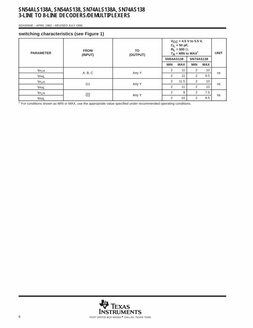
switching characteristics (see Figure 1)
PARAMETERFROM
(INPUT)TO
(OUTPUT)
VCC = 4.5 V to 5.5 V,CL = 50 pF,RL = 500 Ω,TA = MIN to MAX ¶ UNIT(INPUT) (OUTPUT)
SN54ALS138A SN74ALS138A
MIN MAX MIN MAX
tPLHA B C Any Y
2 28 5 22ns
tPHLA, B, C Any Y
6 22 6 18ns
tPLHG or G Any Y
2 22 3 17ns
tPHLG or G Any Y
4 21 4 17ns
¶ For conditions shown as MIN or MAX, use the appropriate value specified under recommended operating conditions.
SN54ALS138A, SN54AS138, SN74ALS138A, SN74AS1383-LINE TO 8-LINE DECODERS/DEMULTIPLEXERS
SDAS055E – APRIL 1982 – REVISED JULY 1996
5POST OFFICE BOX 655303 • DALLAS, TEXAS 75265
absolute maximum ratings over operating free-air temperature range (unless otherwise noted) †
Supply voltage, VCC 7 V. . . . . . . . . . . . . . . . . . . . . . . . . . . . . . . . . . . . . . . . . . . . . . . . . . . . . . . . . . . . . . . . . . . . . . . Input voltage, VI 7 V. . . . . . . . . . . . . . . . . . . . . . . . . . . . . . . . . . . . . . . . . . . . . . . . . . . . . . . . . . . . . . . . . . . . . . . . . . . Operating free-air temperature range, TA: SN54AS138 –55°C to 125°C. . . . . . . . . . . . . . . . . . . . . . . . . . . . . .
SN74AS138 0°C to 70°C. . . . . . . . . . . . . . . . . . . . . . . . . . . . . . . . . . Storage temperature range, Tstg –65°C to 150°C. . . . . . . . . . . . . . . . . . . . . . . . . . . . . . . . . . . . . . . . . . . . . . . . . .
† Stresses beyond those listed under “absolute maximum ratings” may cause permanent damage to the device. These are stress ratings only, andfunctional operation of the device at these or any other conditions beyond those indicated under “recommended operating conditions” is notimplied. Exposure to absolute-maximum-rated conditions for extended periods may affect device reliability.
recommended operating conditions
SN54AS138 SN74AS138UNIT
MIN NOM MAX MIN NOM MAXUNIT
VCC Supply voltage 4.5 5 5.5 4.5 5 5.5 V
VIH High-level input voltage 2 2 V
VIL Low-level input voltage 0.8 0.8 V
IOH High-level output current –2 –2 mA
IOL Low-level output current 20 20 mA
TA Operating free-air temperature –55 125 0 70 °C
electrical characteristics over recommended operating free-air temperature range (unlessotherwise noted)
PARAMETER TEST CONDITIONSSN54AS138 SN74AS138
UNITPARAMETER TEST CONDITIONSMIN TYP‡ MAX MIN TYP‡ MAX
UNIT
VIK VCC = 4.5 V, II = –18 mA –1.2 –1.2 V
VOH VCC = 4.5 V to 5.5 V, IOH = –2 mA VCC –2 VCC –2 V
VOL VCC = 4.5 V, IOL = 20 mA 0.35 0.5 0.35 0.5 V
II VCC = 5.5 V, VI = 7 V 0.1 0.1 mA
IIH VCC = 5.5 V, VI = 2.7 V 20 20 µA
IIL VCC = 5.5 V, VI = 0.4 V –0.5 –0.5 mA
IO§ VCC = 5.5 V, VO = 2.25 V –30 –112 –30 –112 mA
ICCH VCC = 5.5 V 12 17.5 12 17.5 mA
ICCL VCC = 5.5 V 14 20 14 20 mA
‡ All typical values are at VCC = 5 V, TA = 25°C.§ The output conditions have been chosen to produce a current that closely approximates one half of the true short-circuit output current, IOS.
SN54ALS138A, SN54AS138, SN74ALS138A, SN74AS1383-LINE TO 8-LINE DECODERS/DEMULTIPLEXERS
SDAS055E – APRIL 1982 – REVISED JULY 1996
6 POST OFFICE BOX 655303 • DALLAS, TEXAS 75265
switching characteristics (see Figure 1)
PARAMETERFROM
(INPUT)TO
(OUTPUT)
VCC = 4.5 V to 5.5 V,CL = 50 pF,RL = 500 Ω,TA = MIN to MAX † UNIT(INPUT) (OUTPUT)
SN54AS138 SN74AS138
MIN MAX MIN MAX
tPLHA B C Any Y
2 11 2 10ns
tPHLA, B, C Any Y
2 11 2 9.5ns
tPLHG1 Any Y
2 11.5 2 10ns
tPHLG1 Any Y
2 11 2 10ns
tPLHG2 Any Y
2 9 2 7.5ns
tPHLG2 Any Y
2 10 2 8.5ns
† For conditions shown as MIN or MAX, use the appropriate value specified under recommended operating conditions.
SN54ALS138A, SN54AS138, SN74ALS138A, SN74AS1383-LINE TO 8-LINE DECODERS/DEMULTIPLEXERS
SDAS055E – APRIL 1982 – REVISED JULY 1996
7POST OFFICE BOX 655303 • DALLAS, TEXAS 75265
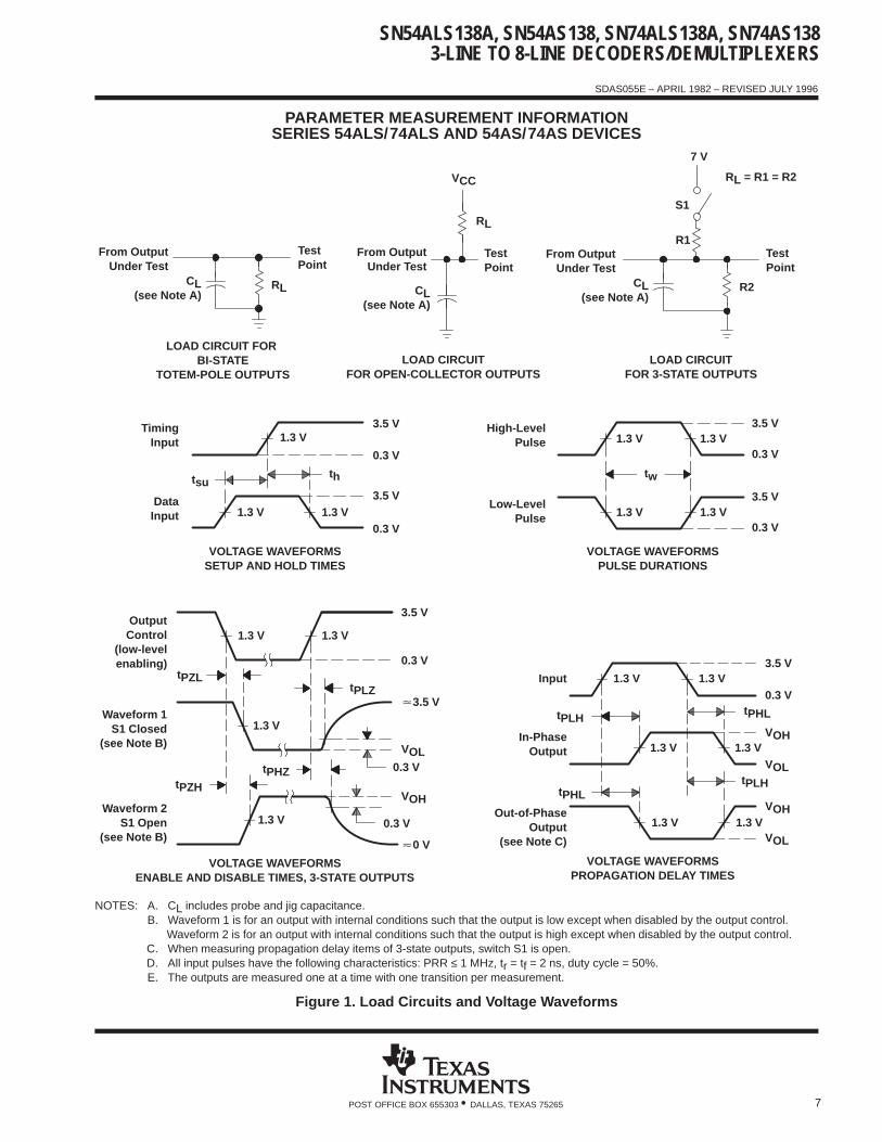
PARAMETER MEASUREMENT INFORMATIONSERIES 54ALS/74ALS AND 54AS/74AS DEVICES
tPHZ
tPLZ
tPHLtPLH
0.3 V
tPZL
tPZH
tPLHtPHL
LOAD CIRCUITFOR 3-STATE OUTPUTS
From OutputUnder Test
Test Point
R1
S1
CL(see Note A)
7 V
1.3 V
1.3 V1.3 V
3.5 V
3.5 V
0.3 V
0.3 V
thtsu
VOLTAGE WAVEFORMSSETUP AND HOLD TIMES
TimingInput
DataInput
1.3 V 1.3 V3.5 V
3.5 V
0.3 V
0.3 V
High-LevelPulse
Low-LevelPulse
tw
VOLTAGE WAVEFORMSPULSE DURATIONS
Input
Out-of-PhaseOutput
(see Note C)
1.3 V 1.3 V
1.3 V1.3 V
1.3 V 1.3 V
1.3 V1.3 V
1.3 V
1.3 V
3.5 V
3.5 V
0.3 V
0.3 V
VOL
VOH
VOH
VOL
OutputControl
(low-levelenabling)
Waveform 1S1 Closed
(see Note B)
Waveform 2S1 Open
(see Note B)0 V
VOH
VOL
3.5 V
In-PhaseOutput
0.3 V
1.3 V 1.3 V
VOLTAGE WAVEFORMSPROPAGATION DELAY TIMES
VOLTAGE WAVEFORMSENABLE AND DISABLE TIMES, 3-STATE OUTPUTS
R2
VCC
RL
Test Point
From OutputUnder Test
CL(see Note A)
LOAD CIRCUITFOR OPEN-COLLECTOR OUTPUTS
LOAD CIRCUIT FOR BI-STATE
TOTEM-POLE OUTPUTS
From OutputUnder Test
Test Point
CL(see Note A)
RL
RL = R1 = R2
NOTES: A. CL includes probe and jig capacitance.B. Waveform 1 is for an output with internal conditions such that the output is low except when disabled by the output control.
Waveform 2 is for an output with internal conditions such that the output is high except when disabled by the output control.C. When measuring propagation delay items of 3-state outputs, switch S1 is open.D. All input pulses have the following characteristics: PRR ≤ 1 MHz, tr = tf = 2 ns, duty cycle = 50%.E. The outputs are measured one at a time with one transition per measurement.
Figure 1. Load Circuits and Voltage Waveforms
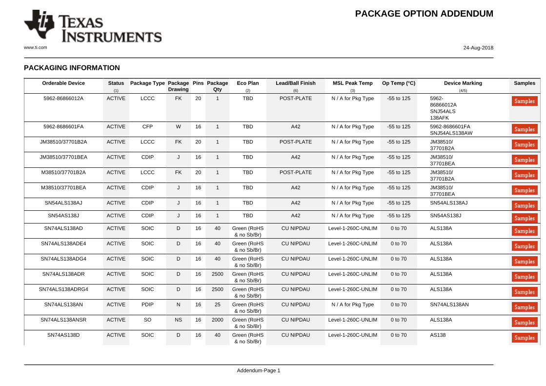
PACKAGE OPTION ADDENDUM
www.ti.com 24-Aug-2018
Addendum-Page 1
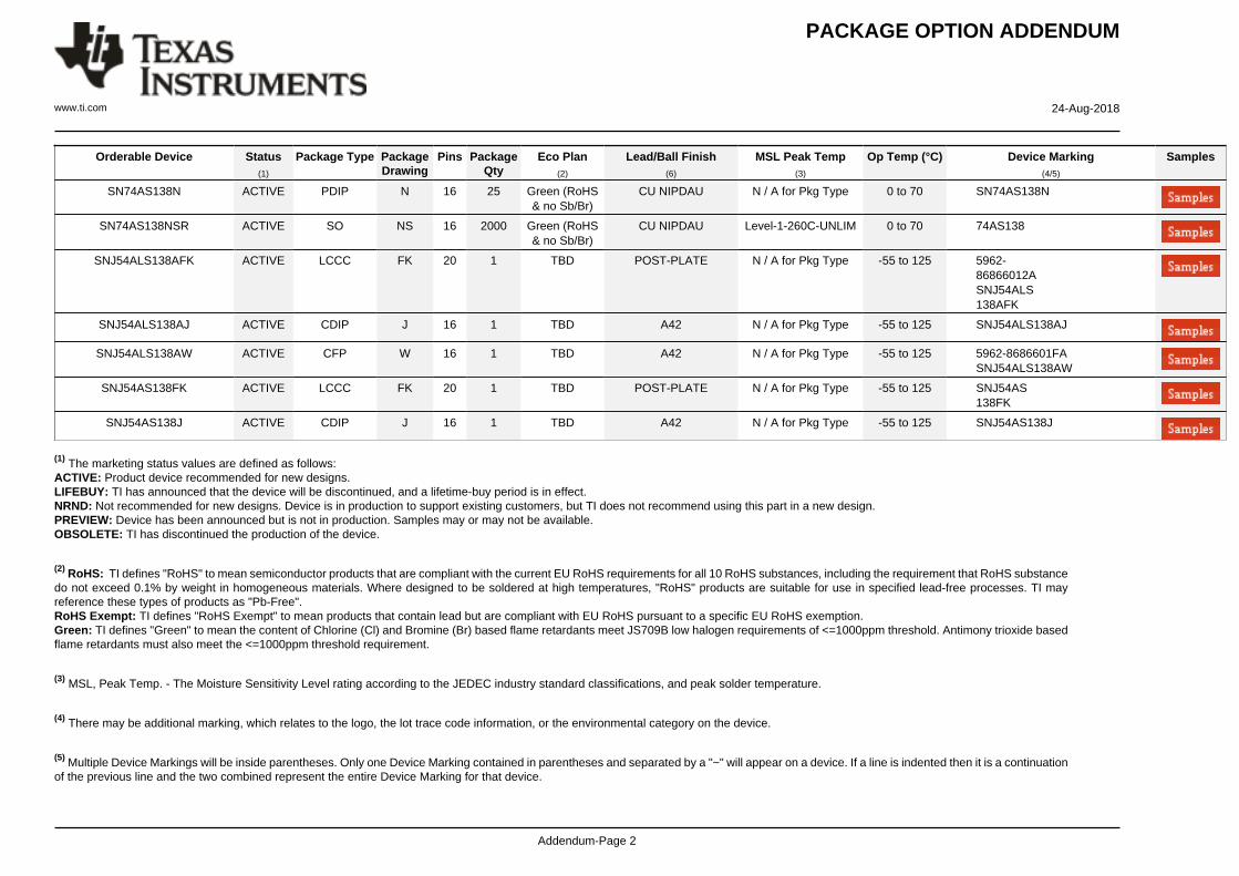
PACKAGING INFORMATION
Orderable Device Status(1)
Package Type PackageDrawing
Pins PackageQty
Eco Plan(2)
Lead/Ball Finish(6)
MSL Peak Temp(3)
Op Temp (°C) Device Marking(4/5)
Samples
5962-86866012A ACTIVE LCCC FK 20 1 TBD POST-PLATE N / A for Pkg Type -55 to 125 5962-86866012ASNJ54ALS138AFK
5962-8686601FA ACTIVE CFP W 16 1 TBD A42 N / A for Pkg Type -55 to 125 5962-8686601FASNJ54ALS138AW
JM38510/37701B2A ACTIVE LCCC FK 20 1 TBD POST-PLATE N / A for Pkg Type -55 to 125 JM38510/37701B2A
JM38510/37701BEA ACTIVE CDIP J 16 1 TBD A42 N / A for Pkg Type -55 to 125 JM38510/37701BEA
M38510/37701B2A ACTIVE LCCC FK 20 1 TBD POST-PLATE N / A for Pkg Type -55 to 125 JM38510/37701B2A
M38510/37701BEA ACTIVE CDIP J 16 1 TBD A42 N / A for Pkg Type -55 to 125 JM38510/37701BEA
SN54ALS138AJ ACTIVE CDIP J 16 1 TBD A42 N / A for Pkg Type -55 to 125 SN54ALS138AJ
SN54AS138J ACTIVE CDIP J 16 1 TBD A42 N / A for Pkg Type -55 to 125 SN54AS138J
SN74ALS138AD ACTIVE SOIC D 16 40 Green (RoHS& no Sb/Br)
CU NIPDAU Level-1-260C-UNLIM 0 to 70 ALS138A
SN74ALS138ADE4 ACTIVE SOIC D 16 40 Green (RoHS& no Sb/Br)
CU NIPDAU Level-1-260C-UNLIM 0 to 70 ALS138A
SN74ALS138ADG4 ACTIVE SOIC D 16 40 Green (RoHS& no Sb/Br)
CU NIPDAU Level-1-260C-UNLIM 0 to 70 ALS138A
SN74ALS138ADR ACTIVE SOIC D 16 2500 Green (RoHS& no Sb/Br)
CU NIPDAU Level-1-260C-UNLIM 0 to 70 ALS138A
SN74ALS138ADRG4 ACTIVE SOIC D 16 2500 Green (RoHS& no Sb/Br)
CU NIPDAU Level-1-260C-UNLIM 0 to 70 ALS138A
SN74ALS138AN ACTIVE PDIP N 16 25 Green (RoHS& no Sb/Br)
CU NIPDAU N / A for Pkg Type 0 to 70 SN74ALS138AN
SN74ALS138ANSR ACTIVE SO NS 16 2000 Green (RoHS& no Sb/Br)
CU NIPDAU Level-1-260C-UNLIM 0 to 70 ALS138A
SN74AS138D ACTIVE SOIC D 16 40 Green (RoHS& no Sb/Br)
CU NIPDAU Level-1-260C-UNLIM 0 to 70 AS138
PACKAGE OPTION ADDENDUM
www.ti.com 24-Aug-2018
Addendum-Page 2
Orderable Device Status(1)
Package Type PackageDrawing
Pins PackageQty
Eco Plan(2)
Lead/Ball Finish(6)
MSL Peak Temp(3)
Op Temp (°C) Device Marking(4/5)
Samples
SN74AS138N ACTIVE PDIP N 16 25 Green (RoHS& no Sb/Br)
CU NIPDAU N / A for Pkg Type 0 to 70 SN74AS138N
SN74AS138NSR ACTIVE SO NS 16 2000 Green (RoHS& no Sb/Br)
CU NIPDAU Level-1-260C-UNLIM 0 to 70 74AS138
SNJ54ALS138AFK ACTIVE LCCC FK 20 1 TBD POST-PLATE N / A for Pkg Type -55 to 125 5962-86866012ASNJ54ALS138AFK
SNJ54ALS138AJ ACTIVE CDIP J 16 1 TBD A42 N / A for Pkg Type -55 to 125 SNJ54ALS138AJ
SNJ54ALS138AW ACTIVE CFP W 16 1 TBD A42 N / A for Pkg Type -55 to 125 5962-8686601FASNJ54ALS138AW
SNJ54AS138FK ACTIVE LCCC FK 20 1 TBD POST-PLATE N / A for Pkg Type -55 to 125 SNJ54AS138FK
SNJ54AS138J ACTIVE CDIP J 16 1 TBD A42 N / A for Pkg Type -55 to 125 SNJ54AS138J
(1) The marketing status values are defined as follows:ACTIVE: Product device recommended for new designs.LIFEBUY: TI has announced that the device will be discontinued, and a lifetime-buy period is in effect.NRND: Not recommended for new designs. Device is in production to support existing customers, but TI does not recommend using this part in a new design.PREVIEW: Device has been announced but is not in production. Samples may or may not be available.OBSOLETE: TI has discontinued the production of the device.
(2) RoHS: TI defines "RoHS" to mean semiconductor products that are compliant with the current EU RoHS requirements for all 10 RoHS substances, including the requirement that RoHS substancedo not exceed 0.1% by weight in homogeneous materials. Where designed to be soldered at high temperatures, "RoHS" products are suitable for use in specified lead-free processes. TI mayreference these types of products as "Pb-Free".RoHS Exempt: TI defines "RoHS Exempt" to mean products that contain lead but are compliant with EU RoHS pursuant to a specific EU RoHS exemption.Green: TI defines "Green" to mean the content of Chlorine (Cl) and Bromine (Br) based flame retardants meet JS709B low halogen requirements of <=1000ppm threshold. Antimony trioxide basedflame retardants must also meet the <=1000ppm threshold requirement.
(3) MSL, Peak Temp. - The Moisture Sensitivity Level rating according to the JEDEC industry standard classifications, and peak solder temperature.
(4) There may be additional marking, which relates to the logo, the lot trace code information, or the environmental category on the device.
(5) Multiple Device Markings will be inside parentheses. Only one Device Marking contained in parentheses and separated by a "~" will appear on a device. If a line is indented then it is a continuationof the previous line and the two combined represent the entire Device Marking for that device.
PACKAGE OPTION ADDENDUM
www.ti.com 24-Aug-2018
Addendum-Page 3
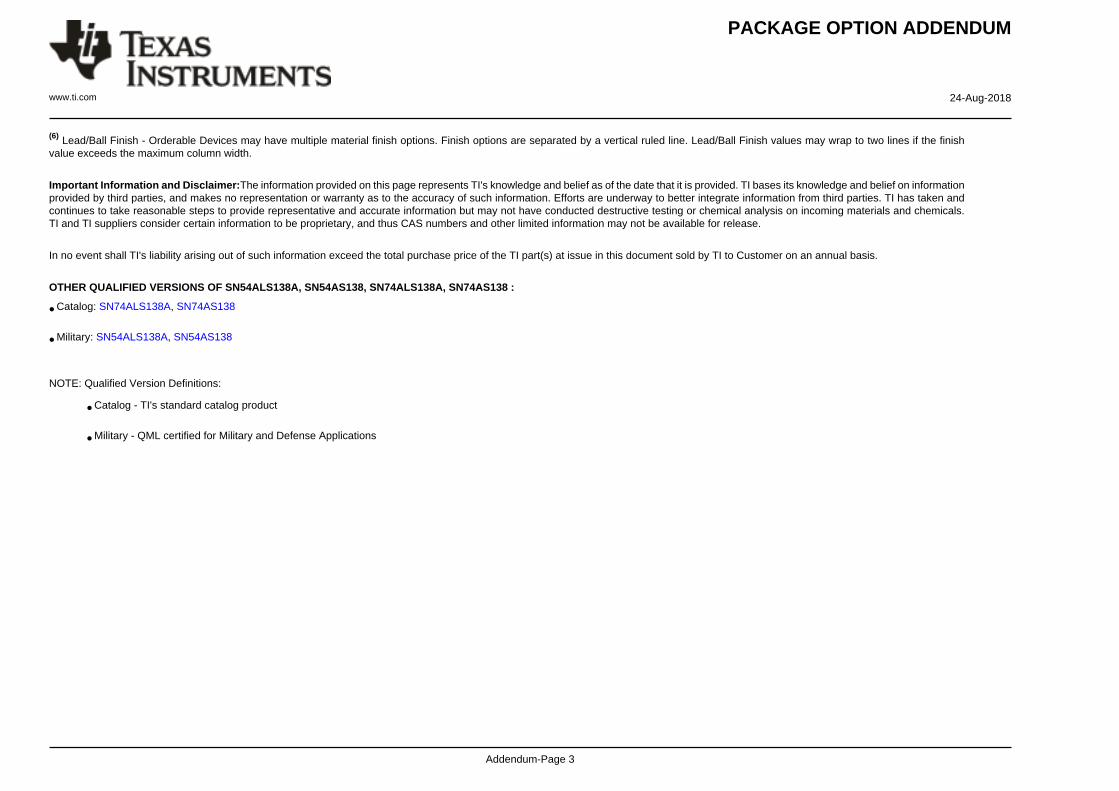
(6) Lead/Ball Finish - Orderable Devices may have multiple material finish options. Finish options are separated by a vertical ruled line. Lead/Ball Finish values may wrap to two lines if the finishvalue exceeds the maximum column width.
Important Information and Disclaimer:The information provided on this page represents TI's knowledge and belief as of the date that it is provided. TI bases its knowledge and belief on informationprovided by third parties, and makes no representation or warranty as to the accuracy of such information. Efforts are underway to better integrate information from third parties. TI has taken andcontinues to take reasonable steps to provide representative and accurate information but may not have conducted destructive testing or chemical analysis on incoming materials and chemicals.TI and TI suppliers consider certain information to be proprietary, and thus CAS numbers and other limited information may not be available for release.
In no event shall TI's liability arising out of such information exceed the total purchase price of the TI part(s) at issue in this document sold by TI to Customer on an annual basis.
OTHER QUALIFIED VERSIONS OF SN54ALS138A, SN54AS138, SN74ALS138A, SN74AS138 :
• Catalog: SN74ALS138A, SN74AS138
• Military: SN54ALS138A, SN54AS138
NOTE: Qualified Version Definitions:
• Catalog - TI's standard catalog product
• Military - QML certified for Military and Defense Applications
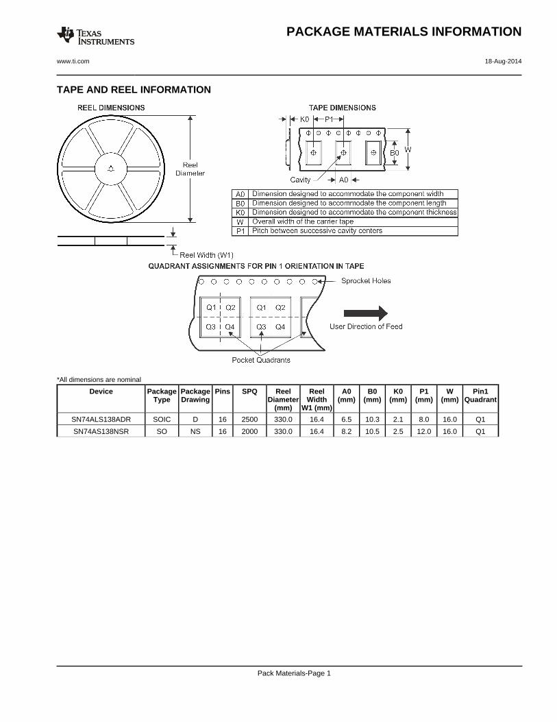
TAPE AND REEL INFORMATION
*All dimensions are nominal
Device PackageType
PackageDrawing
Pins SPQ ReelDiameter
(mm)
ReelWidth
W1 (mm)
A0(mm)
B0(mm)
K0(mm)
P1(mm)
W(mm)
Pin1Quadrant
SN74ALS138ADR SOIC D 16 2500 330.0 16.4 6.5 10.3 2.1 8.0 16.0 Q1
SN74AS138NSR SO NS 16 2000 330.0 16.4 8.2 10.5 2.5 12.0 16.0 Q1
PACKAGE MATERIALS INFORMATION
www.ti.com 18-Aug-2014
Pack Materials-Page 1
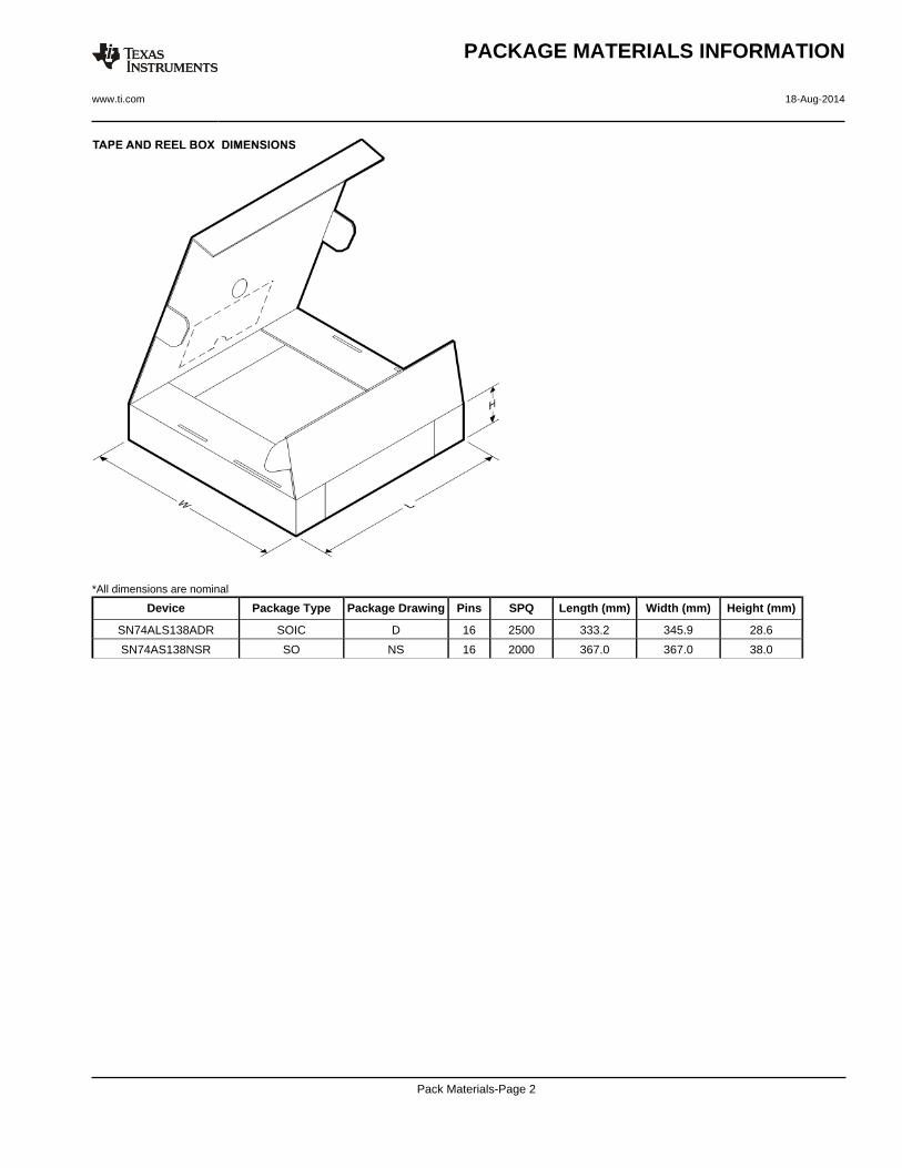
*All dimensions are nominal
Device Package Type Package Drawing Pins SPQ Length (mm) Width (mm) Height (mm)
SN74ALS138ADR SOIC D 16 2500 333.2 345.9 28.6
SN74AS138NSR SO NS 16 2000 367.0 367.0 38.0
PACKAGE MATERIALS INFORMATION
www.ti.com 18-Aug-2014
Pack Materials-Page 2
IMPORTANT NOTICE
Texas Instruments Incorporated (TI) reserves the right to make corrections, enhancements, improvements and other changes to itssemiconductor products and services per JESD46, latest issue, and to discontinue any product or service per JESD48, latest issue. Buyersshould obtain the latest relevant information before placing orders and should verify that such information is current and complete.TI’s published terms of sale for semiconductor products (http://www.ti.com/sc/docs/stdterms.htm) apply to the sale of packaged integratedcircuit products that TI has qualified and released to market. Additional terms may apply to the use or sale of other types of TI products andservices.Reproduction of significant portions of TI information in TI data sheets is permissible only if reproduction is without alteration and isaccompanied by all associated warranties, conditions, limitations, and notices. TI is not responsible or liable for such reproduceddocumentation. Information of third parties may be subject to additional restrictions. Resale of TI products or services with statementsdifferent from or beyond the parameters stated by TI for that product or service voids all express and any implied warranties for theassociated TI product or service and is an unfair and deceptive business practice. TI is not responsible or liable for any such statements.Buyers and others who are developing systems that incorporate TI products (collectively, “Designers”) understand and agree that Designersremain responsible for using their independent analysis, evaluation and judgment in designing their applications and that Designers havefull and exclusive responsibility to assure the safety of Designers' applications and compliance of their applications (and of all TI productsused in or for Designers’ applications) with all applicable regulations, laws and other applicable requirements. Designer represents that, withrespect to their applications, Designer has all the necessary expertise to create and implement safeguards that (1) anticipate dangerousconsequences of failures, (2) monitor failures and their consequences, and (3) lessen the likelihood of failures that might cause harm andtake appropriate actions. Designer agrees that prior to using or distributing any applications that include TI products, Designer willthoroughly test such applications and the functionality of such TI products as used in such applications.TI’s provision of technical, application or other design advice, quality characterization, reliability data or other services or information,including, but not limited to, reference designs and materials relating to evaluation modules, (collectively, “TI Resources”) are intended toassist designers who are developing applications that incorporate TI products; by downloading, accessing or using TI Resources in anyway, Designer (individually or, if Designer is acting on behalf of a company, Designer’s company) agrees to use any particular TI Resourcesolely for this purpose and subject to the terms of this Notice.TI’s provision of TI Resources does not expand or otherwise alter TI’s applicable published warranties or warranty disclaimers for TIproducts, and no additional obligations or liabilities arise from TI providing such TI Resources. TI reserves the right to make corrections,enhancements, improvements and other changes to its TI Resources. TI has not conducted any testing other than that specificallydescribed in the published documentation for a particular TI Resource.Designer is authorized to use, copy and modify any individual TI Resource only in connection with the development of applications thatinclude the TI product(s) identified in such TI Resource. NO OTHER LICENSE, EXPRESS OR IMPLIED, BY ESTOPPEL OR OTHERWISETO ANY OTHER TI INTELLECTUAL PROPERTY RIGHT, AND NO LICENSE TO ANY TECHNOLOGY OR INTELLECTUAL PROPERTYRIGHT OF TI OR ANY THIRD PARTY IS GRANTED HEREIN, including but not limited to any patent right, copyright, mask work right, orother intellectual property right relating to any combination, machine, or process in which TI products or services are used. Informationregarding or referencing third-party products or services does not constitute a license to use such products or services, or a warranty orendorsement thereof. Use of TI Resources may require a license from a third party under the patents or other intellectual property of thethird party, or a license from TI under the patents or other intellectual property of TI.TI RESOURCES ARE PROVIDED “AS IS” AND WITH ALL FAULTS. TI DISCLAIMS ALL OTHER WARRANTIES ORREPRESENTATIONS, EXPRESS OR IMPLIED, REGARDING RESOURCES OR USE THEREOF, INCLUDING BUT NOT LIMITED TOACCURACY OR COMPLETENESS, TITLE, ANY EPIDEMIC FAILURE WARRANTY AND ANY IMPLIED WARRANTIES OFMERCHANTABILITY, FITNESS FOR A PARTICULAR PURPOSE, AND NON-INFRINGEMENT OF ANY THIRD PARTY INTELLECTUALPROPERTY RIGHTS. TI SHALL NOT BE LIABLE FOR AND SHALL NOT DEFEND OR INDEMNIFY DESIGNER AGAINST ANY CLAIM,INCLUDING BUT NOT LIMITED TO ANY INFRINGEMENT CLAIM THAT RELATES TO OR IS BASED ON ANY COMBINATION OFPRODUCTS EVEN IF DESCRIBED IN TI RESOURCES OR OTHERWISE. IN NO EVENT SHALL TI BE LIABLE FOR ANY ACTUAL,DIRECT, SPECIAL, COLLATERAL, INDIRECT, PUNITIVE, INCIDENTAL, CONSEQUENTIAL OR EXEMPLARY DAMAGES INCONNECTION WITH OR ARISING OUT OF TI RESOURCES OR USE THEREOF, AND REGARDLESS OF WHETHER TI HAS BEENADVISED OF THE POSSIBILITY OF SUCH DAMAGES.Unless TI has explicitly designated an individual product as meeting the requirements of a particular industry standard (e.g., ISO/TS 16949and ISO 26262), TI is not responsible for any failure to meet such industry standard requirements.Where TI specifically promotes products as facilitating functional safety or as compliant with industry functional safety standards, suchproducts are intended to help enable customers to design and create their own applications that meet applicable functional safety standardsand requirements. Using products in an application does not by itself establish any safety features in the application. Designers mustensure compliance with safety-related requirements and standards applicable to their applications. Designer may not use any TI products inlife-critical medical equipment unless authorized officers of the parties have executed a special contract specifically governing such use.Life-critical medical equipment is medical equipment where failure of such equipment would cause serious bodily injury or death (e.g., lifesupport, pacemakers, defibrillators, heart pumps, neurostimulators, and implantables). Such equipment includes, without limitation, allmedical devices identified by the U.S. Food and Drug Administration as Class III devices and equivalent classifications outside the U.S.TI may expressly designate certain products as completing a particular qualification (e.g., Q100, Military Grade, or Enhanced Product).Designers agree that it has the necessary expertise to select the product with the appropriate qualification designation for their applicationsand that proper product selection is at Designers’ own risk. Designers are solely responsible for compliance with all legal and regulatoryrequirements in connection with such selection.Designer will fully indemnify TI and its representatives against any damages, costs, losses, and/or liabilities arising out of Designer’s non-compliance with the terms and provisions of this Notice.
Mailing Address: Texas Instruments, Post Office Box 655303, Dallas, Texas 75265Copyright © 2018, Texas Instruments Incorporated


