AN1376APPLICATION NOTE
25W QUASI-RESONANT FLYBACK CONVERTER FORSET-TOP BOX APPLICATION USING THE L6565
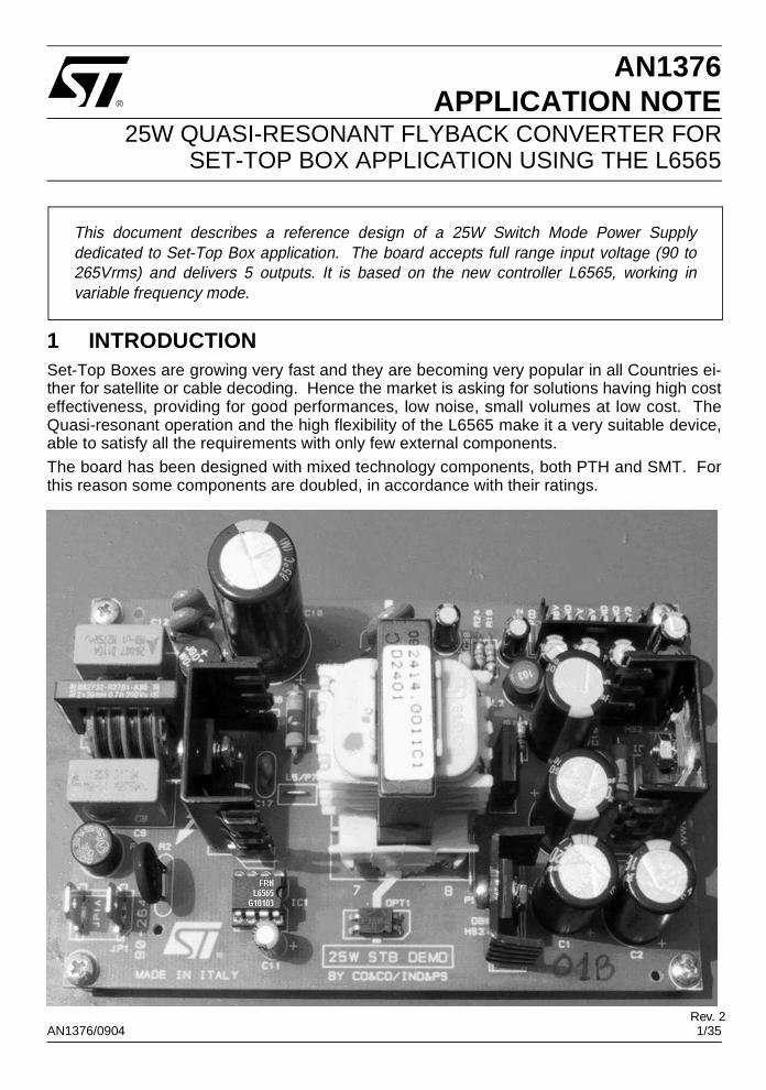
This document describes a reference design of a 25W Switch Mode Power Supplydedicated to Set-Top Box application. The board accepts full range input voltage (90 to265Vrms) and delivers 5 outputs. It is based on the new controller L6565, working invariable frequency mode.
1 INTRODUCTIONSet-Top Boxes are growing very fast and they are becoming very popular in all Countries ei-ther for satellite or cable decoding. Hence the market is asking for solutions having high costeffectiveness, providing for good performances, low noise, small volumes at low cost. TheQuasi-resonant operation and the high flexibility of the L6565 make it a very suitable device,able to satisfy all the requirements with only few external components.
The board has been designed with mixed technology components, both PTH and SMT. Forthis reason some components are doubled, in accordance with their ratings.
Rev. 2
1/35AN1376/0904
AN1376 APPLICATION NOTE
2 MAIN CHARACTERISTICSThe main characteristics of the SMPS are listed here below:
INPUT VOLTAGE:Vin: 90 - 264 Vrmsf: 45-66 Hz
OUTPUT VOLTAGES:
NOTES:(A) Dedicated to 5V digital circuitry and to 3.3v local post regulators(B) Dedicated to SCART, LNBP21 for satellite STB. For other applications the current is 0.4A(C) Dedicated to 5V local post regulators(D) Dedicated to tuner
STAND-BYNo stand-by mode is foreseen by equipment
OVERCURRENT PROTECTIONOn all outputs, with auto-restart at short protection
PCB TYPE & SIZE:Cu Single Side 35 um, FR-4, 122.5 x 75 mm
SAFETY:In acc. with EN60950, creepage and clearance minimum distance 6.4mm
EMI:In acc. with EN50022 Class B
Vout (V): Iout (A): Pout (W): STABILITY NOTES
3.3 2.00 6.6 +/- 2%
5 1.1 5.5 +/- 2% (A)
12 0.7 8.4 +/- 5% (B)
7 0.5 3.5 +/- 8% (C)
30 0.015 0.45 +/- 2% (D)
POUT (W) = 24.45
2/35

AN1376 APPLICATION NOTE
3 ELECTRICAL DIAGRAM
Figure 1. Electrical Diagram
D1
SM
BY
T0
1-4
00
C1
22
00
uF
-16
V Y
XF
C4
100u
F-1
6V -
YX
F
C8
2N
2-2
KV
(Y
1)
C2
22
00
uF
-16
V Y
XF
2
1
4
3
D2
2W
08
G-G
S
C9
10
0N
F1
FU
SE
2A
C1
04
7u
F-4
00
V
D3
ST
TH
1L
06
U
D4
LL
41
48
R1
27
0K
-12
06
C1
122
uF-2
5V Y
XF
R2
NT
C_
16
R S
23
6
32 1
4
L1
39
mH
- E
PC
OS
Q1
ST
P4
NK
60
ZF
P
T1
24
14
.00
11
re
v. C
1
R3
33
R-0
80
5
R4
10
0K
- 0
80
5
R6
0R47
- 1
/2W
PT
H
C1
21
N0
-1K
VC
13
1N
0-1
KV
R7
2K
7 -
08
05
R8
56
0R
-08
05
R9
82
R -
08
05
R1
02
20
R -
08
05
IC2
TL
43
1A
CD
- S
O-8
C1
43
30
N -
12
06
C1
5N
OT
MO
UN
TE
D
R1
14
K7
- 0
80
5
R1
24
70
K-1
20
6C
16
10
0N
R1
3N
OT
MO
UN
TE
D
C1
722
0PF
-1K
V H
RR
FB
1
ISE
N4
VF
F3
CO
MP
2
OU
T7
ZC
D
5
VC
C8
GN
D6
IC1
L6
56
5 -
DIP
8
C3
2200
uF-1
6V Y
XF
R1
42
70
K-1
20
6R
15
47
0K
-12
06
D1
0B
ZV
55
-C1
5C
18
22
uF
-50
V Y
XF
D6
ST
PS
2H
10
0U
C1
922
00uF
-16V
- Y
XF
TO-2
20
HE
AT
SIN
KC
510
0uF
-16V
- Y
XF
L2
10
u E
LC
06
D
C6
100u
F-1
6V -
YX
F
L3
10
u E
LC
06
DC
710
0uF
-16V
- Y
XF
L4
2u
7 E
LC
08
D
C2
022
uF-5
0V Y
XF
1 2
4 3
OP
T1
SF
H6
17
A-4
JP
1
FA
ST
ON
6m
m
JP
1A
FA
ST
ON
6m
m
8 9
1011
121314
2 4 6 7
D7
ST
PS
10
L6
0F
P
D8
ST
PS
10
L6
0F
PTO
-22
0 H
EA
T S
INK
D9
SM
CJ
13
0C
A
AB
L LS
22
0
AB
L LS
22
0TO
-22
0 H
EA
T S
INK
R1
91K
0 -
1/2W
PT
H
R2
01
0K
- 1
20
6
R2
14
70
R -
12
06
R2
20
R0
- 0
80
5
C2
108
05 -
NO
T M
OU
NTE
D
D1
1B
ZV
55
-C1
5
C2
22
20
PF
-08
05
C2
31
N0
-08
05
R2
3N
OT
MO
UN
TE
D
GN
DVO
UT
VIN
IC3
LD
10
86
V5
0
C2
710
0N -
080
5
C2
81
00
N -
08
05
C2
51
00
N -
08
05
C2
61
00
N -
08
05
C2
41
00
N -
08
05
18
12
V @
0.7
A
30
V @
0.0
15
A
7V
@0
.5A
5V
@1
.1A
3.3
V @
2A
GN
D
GN
D
GN
D
R2
41
80
R 1
/2W
PT
H
C3
02
20
PF
-1K
V H
RR R
18
47
R
- 1
/2W
PT
H
P8
JU
MP
ER
R2
82
4K
-08
05
C3
31
00
N -
08
05
R2
71
20
K -
08
05
D1
2L
L4
14
8
Q3
BC
84
7B
Q4
BC
84
7B
R2
61
K0
- 0
80
6
R2
51
K8
- 0
80
6
D5
LL
41
48
C3
22
N2
- 0
80
5
Q2
BC
85
6C
31
22
0P
- 0
80
5
R5
3K
3 -
08
05
D9
AN
OT
MO
UN
TED
R1
647
0R -
1/2
W P
TH
R1
71R
0 -
2W -
PT
HC
29
100N
- 0
805
JP
2M
KS
18
58
-6-0
-80
8
GB
IP
TH
3/35

AN1376 APPLICATION NOTE
The switching frequency (minimum is ~30 kHz @Vin = 80 VDC) has been chosen to get a com-promise between the transformer size and the harmonics of the switching frequency, in orderto optimise the input filter size and its cost. The MOSFET is a standard and cheap 600V-1.76Ωtyp., TO-220FP. It needs a small heat sink. The transformer reflected voltage is 90V, providingenough room for the leakage inductance voltage spike with still margin for reliability. The net-work D9+D3 clamps the peak of the leakage inductance voltage spike. These two componentsare SMT, allowing cost saving of the manual labour with respect to a passive solution, needingmanual insertion on the PCB. A 220pF HV capacitor has been added across the drain to opti-mise MOSFET losses by a small snubbing effect on the drain voltage rate of rise.
The controller L6565 is activated by a couple of dropping resistors (R1+R14, for voltage andpower rating reasons) that draws current from the DC bus and charges the capacitor C11. Thiscircuit dissipates only about 240mW @ 264 Vac, thanks to the extremely low start-up current.During the normal operation the controller is powered by the transformer via the diode D4. Thenetwork Q101, C102, R104 acts as a spike killer, improving the auxiliary voltage fluctuationsand the performance in short circuit. R12+R15 and R11 compensate for the power capabilitychange vs. the input voltage (Voltage Feed-forward). A 1nF ceramic capacitor bypasses anynoise on pin #3 to ground (C23). The current flowing in the transformer primary is sensed bythe resistor R6. The circuit connected to pin1 (FB) provides for the over voltage protection incase of feedback network failures and open loop operation.
The output rectifiers have been chosen in accordance with the maximum reverse voltage andpower dissipation. The rectifiers for 3.3V and 7V outputs are Schottky, type STPS10L60FP.These diodes are low forward voltage drop, hence dissipating less power with respect to stan-dard types. Both are the same to decrease the component diversity, as well as for the capac-itors C1 to C3 and C19. The diode D8 needs a small heat sink, as indicated on the BOM. Theother two output rectifiers are SMT, fast recovery. The snubber R102 and C101 damps the os-cillation produced by the diode D1 at MOSFET turn-on.
The output voltage regulation is performed by secondary feedback on the 3.3V output, whilefor other voltages the regulation is achieved by the transformer coupling. The feedback net-work is the classical TL431 driving an optocoupler, in this case an SFH617A-4, insuring therequired insulation between primary and secondary. The opto-transistor drives directly theCOMP pin of the controller. The 5V output is linearly post-regulated from the 7V output to geta very stable voltage. A zener regulator assures the 30V stability at low cost. The 5V regulatorneeds to be dissipated.
A small LC filter has been added on the +12V, +7V, +3.3V in order to filter the high frequencyripple without increasing the output capacitors.
A 100nF capacitor has been connected on each output, very close to the output connector sol-dering points to limit the spike amplitude.
The input EMI filter is a classical Pi-filter, 1-cell for differential and common mode noise. A NTClimits the inrush current produced by the capacitor charging at plug-in.
The transformer is slot type, manufactured by Eldor Corporation, in accordance with theEN60950.
Here following some waveforms during the normal operation at full load:
4/35

AN1376 APPLICATION NOTE
Figure 2. Vds & Id @ Full Load
The pictures above show the drain voltage and current at the nominal input mains voltage dur-ing normal operation at full load. The Envelope acquisition of the scope provides for the pos-sibility to see the modulation of the two waveforms due to the input voltage ripple.
Figure 3. Vds & Id @ Full Load (Vin = 265 Vrms - 50 Hz)
Figure 4. Vin = 265 Vrms - 50 Hz, @FULL LOAD: DIODE PIV
Vin = 115 Vrms - 50 Hz Vin = 220 Vrms - 50 Hz
CH1: DRAIN VOLTAGE;CH2: RAIN CURRENT - VR.SENSE (R6)
CH1: DRAIN VOLTAGE;CH2: RAIN CURRENT - VR.SENSE (R6)
This picture gives the measurement of thedrain peak voltage at full load and maximuminput mains voltage. The voltage peak, whichis 548V, assures a reliable operation of thePowerMOS with a good margin against themaximum BVDSS.
CH3: +35V DIODE: ANODE VOLTAGE;CH4: +12V DIODE: ANODE VOLTAGE
CH3: +7V DIODE: ANODE VOLTAGE;CH4: +3V3 DIODE: ANODE VOLTAGE
5/35

AN1376 APPLICATION NOTE
The maximum PIV of the diodes has been measured during the worst operating condition andit is indicated on the right of each picture. The margin, with respect to the maximum voltagesustained by the diodes, assures a safe operating condition for the devices.
Here following the most salient controller IC signals are depicted. In both the pictures is pos-sible to distinguish clean waveforms free of hard spikes or noise that could affect the controllercorrect operation.
Figure 5. Vin = 115 Vrms - 50 Hz Vin = 220 Vrms - 50 Hz
4 CROSS REGULATIONIn the following tables the output voltage cross regulation is measured with static and dynamicloads and the overall efficiency of the converter measured at different input voltages. All theoutput voltages have been measured after the load connector soldering point of the STBmotherboard. The length of the connection cable is 100 mm.
FULL LOAD
Vout [V = 30.06 7.23 12.297 3.278 4.492 Vin [Vrms]= 115
Iout [A] = 0.015 0.500 0.702 2.073 1.103 Iin [Arms] = 0.51
Pout [W] = 0.451 3.615 8.632 6.795 4.955 Pin [W] = 36.0
VUNREG = 37.2 PoutTOT [W] = 24.448
VC11 = 11.88 EFF. = 67.91%
fS = 41÷51 kHz ALL VOLTAGES ARE WITHIN TOLERANCE
CH1: VPIN5 - ZCD
CH2: VPIN4 - ISENSE
CH3: VPIN7 - OUT
CH4: VPIN2 - COMP
6/35

AN1376 APPLICATION NOTE
The efficiency of the converter is not very high but it is heavily affected by 5V the linear regu-lator delivering 1.1 A. Delivering 1.6A on the 7V output but removing the 5V regulator the ef-ficiency measured is 75.6% @220Vac and 76.9% at 115Vac.
Reduced Load - for Cable STB, without the LNB
The above tables shown the output voltage measured applying the same loads that we couldhave in case of a different Set-top Box type is powered (e.g. a terrestrial or cable) without theLNB block of the satellite antenna. Like before all the output voltages are within the toleranc-es.
Vout [V = 30.5 7.197 12.19 3.279 4.94 Vin [Vrms]= 220
Iout [A] = 0.015 0.5 0.702 2.073 1.103 Iin [Arms] = 0.31
Pout [W] = 0.458 3.599 8.557 6.797 5.449 Pin [W] = 35.1
VUNREG = 37.2 PoutTOT [W] = 24.860
VC11 = 12.04 EFF. = 70.82%
fS = 66÷68 kHz ALL VOLTAGES ARE WITHIN TOLERANCE
Vout [V = 31.4 7.18 12.11 3.359 4.965 Vin [Vrms]= 115
Iout [A] = 0 0.25 0.3 1.008 0.55 Iin [Arms] = 0.26
Pout [W] = 0.000 1.795 3.633 3.386 2.731 Pin [W] = 16.8
VUNREG = 35.5 PoutTOT [W] = 11.545
VC11 = 11.39 EFF. = 68.72%
fS = 83÷89 kHz ALL VOLTAGES ARE WITHIN TOLERANCE
Vout [V = 31.4 7.16 12.08 3.36 4.975 Vin [Vrms]= 220
Iout [A] = 0 0.25 0.3 1.008 0.55 Iin [Arms] = 0.17
Pout [W] = 0.000 1.790 3.624 3.387 2.736 Pin [W] = 17.6
VUNREG = 35.4 PoutTOT [W] = 11.537
VC11 = 11.5 EFF. = 65.55%
fS = 112 kHz ALL VOLTAGES ARE WITHIN TOLERANCE
7/35

AN1376 APPLICATION NOTE
Reduced Load - 9W
Even still reducing the load till 9W, Thanks to the good coupling of the transformer, all the out-put voltages are still in tolerance.
At No-Load (Output connector unplug)
Vout [V = 31.6 7.16 12.77 3.36 4.96 Vin [Vrms]= 115
Iout [A] = 0 0.300 0.051 1.008 0.6 Iin [Arms] = 0.22
Pout [W] = 0.000 2.148 0.651 3.387 2.976 Pin [W] = 14.2
VUNREG = 36 PoutTOT [W] = 9.162
VC11 = 11.48 EFF. = 64.52%
fS = 94÷101 kHz ALL VOLTAGES ARE WITHIN TOLERANCE
Vout [V = 31.5 7.16 12.76 3.36 4.96 Vin [Vrms]= 220
Iout [A] = 0 0.300 0.051 1.008 0.602 Iin [Arms] = 0.15
Pout [W] = 0.000 2.148 0.651 3.387 2.986 Pin [W] = 15.2
VUNREG = 35.8 PoutTOT [W] = 9.172
VC11 = 11.7 EFF. = 60.34%
fS = PFM/PWM ALL VOLTAGES ARE WITHIN TOLERANCE
Vout [V] = 30.4 7.20 12.15 3.39 5.00 Vin [Vrms]= 220
Pin [W] = 1.6
Vin [Vrms]= 115
Vout [V] = 30.4 7.20 12.0 3.38 5.00 Pin [W] = 1.5
8/35

AN1376 APPLICATION NOTE
Figure 6.
Vin = 115 Vrms - 50 HzUnplugging the output connector the circuitis still able to maintain all the voltages per-fectly under control and within the tolerance.Hence a perfect functionality of the circuit isachieved also in this abnormal condition.During the no load operation the circuitworks in burst mode and, thanks to the con-troller functionality, the switching frequencyinside the Burst pulses is kept at low. Thisprovides for a low power consumption of thepower supply, making it suitable to supportstand-by operation with low consumptionfrom the mains. It has to be kept into ac-count that this circuit has not been opti-mized for the Stand-by operation, hence itcould be improved.
Vin = 220 Vrms - 50 Hz
CH1: VPIN5 - ZCD
CH2: VPIN4 - ISENSE
CH3: VPIN7 - OUT
CH4: VPIN2 - COMP
9/35

AN1376 APPLICATION NOTE
5 OUTPUT VOLTAGE RIPPLE @FULL LOADIn the following picture all the output voltage ripple at switching and mains frequency are mea-sured. As per the previous measures, the probes have been connected on test points after theoutput flat cable. As shown in the pictures, the ripple and the spikes are very low.
Figure 7.
@115 VAC - 50Hz
@220 VAC - 50Hz
CH2: +7 Vout CH2: +30 Vout
CH3: +3.3 Vout CH3: +5 Vout
CH4: +12 Vout
10/35

AN1376 APPLICATION NOTE
Figure 8.
The low frequency residual ripple compared with the ripple across C10 (input Elcap) shows anexcellent rejection of the circuit (>80 dB).
6 MEASUREMENT OF THE RMS CAPACITOR CURRENTSThe tables show the rms currents flowing in the output capacitors at 115Vac and 220Vac, fullload. All the rms currents are within the rating of the capacitor type indicated (Rubycon, YXFseries). This avoids the component overstress that should affect the reliability and/or the ex-pected lifetime of the SMPS.
@ 115Vac: ICAP C1 = 1.02 ARMS @ 115Vac: ICAP C3 = 1.78 ARMS
@ 115Vac: ICAP C19 = 1.15 ARMS @ 115Vac: ICAP C18 = 140 mARMS
@ 220Vac: ICAP C1 = 0.7 ARMS @ 220Vac: ICAP C1 = 1.4 ARMS
@ 220Vac: ICAP C19 = 0.92 ARMS @ 220Vac: ICAP C18 = 130 mARMS
@115 VAC - 50Hz - LINE FREQUENCY RIPPLE
CH1: VC10 CH2: +30 Vout
CH2: +7 Vout CH3: +5 Vout
CH3: +3.3 Vout
CH4: +12 Vout
11/35

AN1376 APPLICATION NOTE
7 DYNAMIC LOAD TESTSRegulated Output
Figure 9.
The pictures show the output voltage regulation against a dynamic load variation of the feedbacked voltage, at the nominal input voltage values. As shown in the left pictures the responseafter the connector is not very good from the peak point of view, even if the response is quitefast. Making the same measure before the filter inductor (L4), at the feed back divider connec-tion points, the response is much better (≈2.2 %). This means that the filter inductor heavily
Load condition: +5V, +7V, +12V, +30V: FULL LOAD
+3,3V: LOAD 50 %÷100%, 70Hz
@115 VAC - 50Hz
@220 VAC - 50Hz
CH3: +3V3 Vout at test points CH1: +30 Vout
CH4: +3V3 Iout CH2: +12 Vout
R1: +3V3 Vout before L4 CH3: +7 Vout
CH4: +3V3 Iout
12/35

AN1376 APPLICATION NOTE
affect the response. To avoid any expensive solution to improve it the better way is to measurethe voltage regulation during the normal operation, powering the real load circuitry. This, be-cause there are some local capacitors or filters helping a lot the regulation. Moreover, normallythe dynamic load changes are less than the testing value indicated.
The regulation for all the other output voltage is good, remaining well within tolerances.
Unregulated Outputs
The following tests show the response of the output voltages varying the load for each unreg-ulated output. The load conditions are specified at the right of each picture. The regulationhas been tested at both the nominal mains voltages.
Figure 10. @115 VAC - 50Hz
CH1: +12 Vout
CH2: +7 Vout
CH3: +3V3 Vout
CH4: +5V Iout
+3,3V +5V, +7V, +30V: FULL LOAD
+12V: DYNAMIC LOAD 0.1 to 0.7A, 70Hz
@ 220Vac the waveforms have the sameamplitude.
CH1: +12 Vout
CH2: +7 Vout
CH3: +3V3 Vout
CH4: +12V Iout
+3,3V +5V, +7V, +30V: FULL LOAD
+5V: DYNAMIC LOAD 0.5 to 1.1A, 70Hz
5V modulation: 20 mVpp
@ 220Vac the waveforms have the sameamplitude.
ALL THE VOLTAGES ARE WITHIN TOLERANCES, AT BOTH INPUT MAINS VOLTAGES
13/35

AN1376 APPLICATION NOTE
Figure 11.
8 START-UP BEHAVIOUR @FULL LOAD
Figure 12.
@115 VAC - 50Hz
CH1: +12 Vout CH3: +3V3 Vout
CH2: +7 Vout CH4: +7V Iout
+3,3V +5V, +7V, +30V: FULL LOAD
+7V: DYNAMIC LOAD 0.1 to 0.5A, 70Hz
5V modulation: 20 mVpp
@ 220Vac the waveforms have the sameamplitude.
ALL THE VOLTAGES ARE WITHIN TOL-ERANCES, AT BOTH INPUT MAINSVOLTAGES
@115 VAC - 50Hz @220 VAC - 50Hz
@85 VAC - 50Hz @265 VAC - 50Hz
CH1: +12 Vout CH3: +3.3 Vout CH2: +5 Vout CH4: +7V Iout
14/35

AN1376 APPLICATION NOTE
In the previous 4 pictures there are the rising slopes at full load of the more significant outputvoltages at nominal, minimum and maximum input mains voltage. As shown in the pictures,the rising times are constant and there is only a slight difference for the 5V rise time, with re-spect to the other outputs. This characteristic is quite important when the loads are a µP andits peripherals as in our case, to avoid problem at start-up. At minimum voltage a super im-posed ripple at line frequency is present, due to the high ripple at the input that is not complete-ly rejected by the loop before reaching the steady state operation. This because while the inputvoltage is rising, the ripple valley voltage is less than the minimum operating voltage of the cir-cuit, therefore the ripple it is properly rejected only when it reaches that value.
9 WAKE-UP TIMEIn the following pictures there are the waveforms with the wake-up time measures at the nom-inal input mains. Obviously, due to the circuitry characteristics, the wake-up time is not con-stant but it is dependent on the input voltage. The measured time at 115 and 220 Vac are 1.2and 0.6 second, which are rather common values for this kind of Power Supplies.
The worst condition, of course, is at 85 Vac when the start-up time becomes around 1.7 sec-onds, which is quite a long time even if still acceptable. This because there is anyway the start-up time of the STB which is longer. Additionally, the 85Vac input mains is a steady state volt-age but it is not a very common value.
Figure 13.
In Figure 14 there are the waveforms at minimum and maximum voltage with a magnificationof the time base: on the picture is clearly indicated that no any overshoot, undershoot, dip orlost of control happens during the power supply start-up phase. Obviously also the nominalvoltages are been detected without showing any abnormal behaviour.
@115 VAC - 50Hz @220 VAC - 50Hz
15/35

AN1376 APPLICATION NOTE
Figure 14.
10 TURN-OFFEven at turn off the transition is clean, without any abnormal behaviour like restart or glitchesboth on the primary or secondary side.
Figure 15.
@85 VAC - 50Hz @265 VAC - 50Hz
CH1: VDD CH1: VDD
CH2: VC11 (Vaux) CH2: VC11 (Vaux)
CH3: +3V3 Vout CH3: +3V3 Vout
@85 VAC - 50Hz @265 VAC - 50Hz
CH1: VDD CH1: VDD
CH2: VC11 (Vaux) CH2: VC11 (Vaux)
CH3: +3V3 Vout CH3: +3V3 Vout
16/35

AN1376 APPLICATION NOTE
11 SHORT-CIRCUIT TESTS @ FULL LOADThe short circuit tests have been done in two phases, both making the test shorting by a powerswitch the output electrolytic capacitor or making the short by the active load option. This givesan idea about the circuit behaviour with a hard short (at very low impedance) or with a "soft"short that could happen on the STB main board, having slightly higher impedance. All the testshave been done at maximum and minimum input voltage. For all conditions the drain voltageis always below the BVDSS, while the mean value of the output current has a value close tothe nominal one, then preventing component melting for excessive dissipation. The auto-re-start is correct at short removal in all conditions.
Figure 16. 7V OUTPUT: SHORT C3
As clearly indicated by the waveforms, the circuit start to work in hic-cup mode, so maintaing the meanvalue of the current at levels supported by the component rating. Because the working time and the deadtime are imposed by the charging and discharging time of the auxiliary capacitor C11, it is proportionalto the input mains voltage.
Figure 17. 7V OUTPUT: SHORT BY ACTIVE LOAD
@85 VAC @265 VAC
CH1: DRAIN VOLTAGE CH1: DRAIN VOLTAGE
CH2: VC11 (Vaux) CH2: VC11 (Vaux)
CH4: ISHORT CIRCUIT CH4: ISHORT CIRCUIT
@85 VAC @265 VAC
CH1: DRAIN VOLTAGE CH1: DRAIN VOLTAGE
CH2: VC11 (Vaux) CH2: VC11 (Vaux)
CH4: ISHORT CIRCUIT CH4: ISHORT CIRCUIT
17/35

AN1376 APPLICATION NOTE
As expected the circuit protects itself as well. The secondary peak current is obviously lower,due to the higher circuit impedance.
Figure 18. 3V3 OUTPUT: SHORT C1
Like the previous output voltage the controller keeps under control the circuit preventing in allconditions the circuit from catastrophic failures. This happens even shorting the output by theactive load.
Figure 19. 12V OUTPUT: SHORT C19
Even the 12V output is well protected against shorts, either by a power switch or by the activeload
@85 VAC @265 VAC
CH1: DRAIN VOLTAGE CH1: DRAIN VOLTAGE
CH2: VC11 (Vaux) CH2: VC11 (Vaux)
CH4: ISHORT CIRCUIT CH4: ISHORT CIRCUIT
@85 VAC @265 VAC
CH1: DRAIN VOLTAGE CH1: DRAIN VOLTAGE
CH2: VC11 (Vaux) CH2: VC11 (Vaux)
CH4: ISHORT CIRCUIT CH4: ISHORT CIRCUIT
18/35
AN1376 APPLICATION NOTE
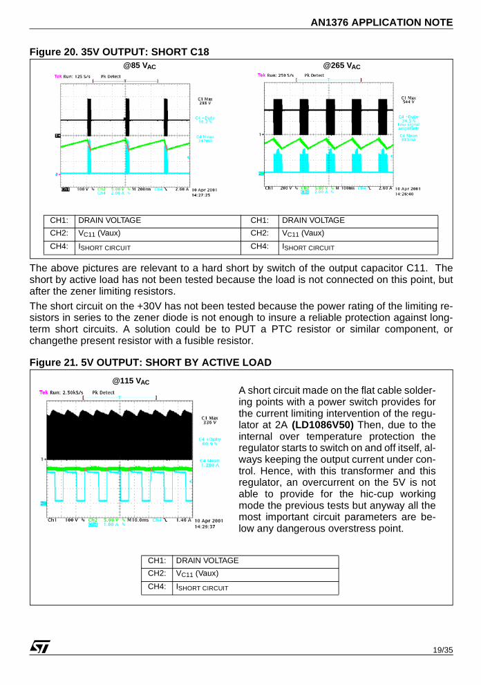
Figure 20. 35V OUTPUT: SHORT C18
The above pictures are relevant to a hard short by switch of the output capacitor C11. Theshort by active load has not been tested because the load is not connected on this point, butafter the zener limiting resistors.
The short circuit on the +30V has not been tested because the power rating of the limiting re-sistors in series to the zener diode is not enough to insure a reliable protection against long-term short circuits. A solution could be to PUT a PTC resistor or similar component, orchangethe present resistor with a fusible resistor.
Figure 21. 5V OUTPUT: SHORT BY ACTIVE LOAD
@85 VAC @265 VAC
CH1: DRAIN VOLTAGE CH1: DRAIN VOLTAGE
CH2: VC11 (Vaux) CH2: VC11 (Vaux)
CH4: ISHORT CIRCUIT CH4: ISHORT CIRCUIT
@115 VACA short circuit made on the flat cable solder-ing points with a power switch provides forthe current limiting intervention of the regu-lator at 2A (LD1086V50) Then, due to theinternal over temperature protection theregulator starts to switch on and off itself, al-ways keeping the output current under con-trol. Hence, with this transformer and thisregulator, an overcurrent on the 5V is notable to provide for the hic-cup workingmode the previous tests but anyway all themost important circuit parameters are be-low any dangerous overstress point.
CH1: DRAIN VOLTAGE
CH2: VC11 (Vaux)
CH4: ISHORT CIRCUIT
19/35

AN1376 APPLICATION NOTE
12 SHORT CIRCUIT PROTECTION @ LOW LOADAfter the full load tests some checks on the short circuit protection with reduced loads havebeen done.
@Half Load
At Vin = 115Vac: shorting each output by the active load the over current protection workscorrectly, providing for the hic-cup working mode, except for the 5V which is protected by thecurrent limiting of the linear regulator.
At Vin = 220Vac: the circuit behaves like at 115V.
@Reduced Load - 1
At Vin = 115Vac: shorting the 3.3V, 7V, 12V and 35V it provides for the hic-cup working modeof the circuit.
At Vin = 220Vac: the behaviour is the same.
@Reduced Load - 2
Both at 115V and 220V the circuit is still protected against short circuits on all the outputs
13 SHORT CIRCUIT PROTECTION @ NO LOAD Even in this abnormal condition, with the output connector unplugged, a short on the outputsprovides for the same results of the previous tests, both at 115Vac or at 220 Vac.
Figure 22. 3.3V OUTPUT: SHORT @NO LOAD
35V 12V 7V 5V 3.3V
15mA 0.25 A 0.35A 0.55A 1A
PoutTOT = 12.6W
35V 12V 7V 5V 3.3V
15mA 0.5 A 0A 0A 1A
PoutTOT = 9.5W
35V 12V 7V 5V 3.3V
15mA 0.4 A 0A 0A 0A
@115 VAC @220 VAC
CH1: DRAIN VOLTAGE CH1: DRAIN VOLTAGE
CH2: VC11 (Vaux) CH2: VC11 (Vaux)
CH3: 3.3V OUTPUT CH4: 3.3V OUTPUT
20/35

AN1376 APPLICATION NOTE
14 SHORT CIRCUIT OF THE OUTPUT RECTIFIERS A frequent problem in a power supply is relevant to the protection of the SMPS itself: thussometimes it is easy to find circuits with a good protection capability against shorts of the loadbut which are not able to survive in case of a very hard short like an output electrolytic capacitoror a diode. Besides, in case of a rectifier shorted the equivalent circuit changes and the energyis delivered even during the on time, like in forward mode.
To insure reliable operation of the design, even this fault condition has been simulated for eachrectifier. Thanks to the controller functionality, the SMPS can withstand this failure, working inburst mode as visible in the pictures,
Figure 23. RECTIFIERS SHORT: @FULL LOAD - 220 VAC
In case of an output diode short, the current sensing voltage exceeds a second protection lev-el, then the controller stops the operation, so avoiding the destruction of the components atprimary side. The controller remains in off-state until the voltage across the Vcc pin decreasesbelow the UVLO threshold. Then it try to restart and it will switch off again until the secondaryshort is removed. This provides for the hic-cup working mode, preventing the circuit destruc-tion. The operating frequency inside the burst is the internal timer one (~2.5 Khz).
7V
CH1: DRAIN VOLTAGE CH1: DRAIN VOLTAGE
CH2: VPIN4 - ISENSE CH2: VPIN4 - ISENSE
12V 35V
CH1: DRAIN VOLTAGE CH1: DRAIN VOLTAGE
CH2: VPIN4 - ISENSE CH2: VPIN4 - ISENSE
3.3V
21/35

AN1376 APPLICATION NOTE
15 SWITCH ON AND TURN OFF IN SHORT CIRCUIT CONDITION FULL LOAD SHORT ON 3V3 BY ACTIVE LOAD
The following pictures describe the SMPS behaviour during the start-up phase with an outputvoltage shorted. As clearly visible the circuit starts correctly then it works in hic-cup mode pro-tecting itself. The start-up phase is clean in all conditions, without showing any dangerous tran-sition for the SMPS circuitry.
Figure 24. START
Figure 25. TURN-OFF
Even at turn off in short circuit the SMPS functionalities are good, protecting properly the cir-cuit. No any abnormal transition or level has been observed during the tests.
@85 VAC - 50Hz @265 VAC - 50Hz
@85 VAC - 50Hz @265 VAC - 50Hz
CH1: VDD CH1: VDD
CH2: VC11 (Vaux) CH2: VC11 (Vaux)
CH3: +3V3 Vout CH3: +3V3 Vout
22/35

AN1376 APPLICATION NOTE
16 OVER VOLTAGE PROTECTIONA dangerous fault that could happen in case is the failure of the feedback circuitry. If this oc-curs, the SMPS output voltages can get high values, depending on the load by each outputand the transformer coupling between the windings. Consequently, the rectifiers and the out-put capacitors are overstressed and can be destroyed. To avoid the SMPS failure a suitableprotection circuit has been added. Then the circuit has been tested opening the loop, givingthe following results:
3.3V OUTPUT: @ full load 3.3V OUTPUT: @ No load
@115V – 50Hz @220V – 50Hz @115V – 50Hz @220V – 50Hz
V3V3: 4.02 V V3V3: 4.08 V V3V3: 4.64 V V3V3: 4.67 V
23/35

AN1376 APPLICATION NOTE
17 CONDUCTED NOISE MEASUREMENTS (Pre-Compliance Test)The following pictures are the peak and quasi-peak conducted noise measurements at fullload and nominal mains voltages. The limits shown on the diagrams are the EN55022 CLASSB ones, which is the most widely rule for domestic equipments like a STB. As visible on thediagrams there is a good margin of the measures with respect to the limits, either in peak orquasi-peak mode.
The detail of the filtering components used is on the right of each diagram.
Figure 26.
PEAK MEASUREBOARD #2
C9 = 100nF EPCOS
L = 39 mH EPCOS
C16 = 100nF EPCOS
TRAFO 2412.0011 REV. C1
Pout = 25W
QUASI-PEAK MEASUREBOARD #2
C9 = 100nF EPCOS
L = 39 mH EPCOS
C16 = 100nF EPCOS
TRAFO 2412.0011 REV. C1
Pout = 25W
Vin = 115 Vrms 50 Hz – FULL LOAD Limits: EN55022 CLASS B
24/35

AN1376 APPLICATION NOTE
Figure 27.
PEAK MEASUREBOARD #2
C9 = 100nF EPCOS
L = 39 mH EPCOS
C16 = 100nF EPCOS
TRAFO 2412.0011 REV. C1
Pout = 25W
QUASI-PEAK MEASUREBOARD #2
C9 = 100nF EPCOS
L = 39 mH EPCOS
C16 = 100nF EPCOS
TRAFO 2412.0011 REV. C1
Pout = 25W
Vin = 220 Vrms 50 Hz – FULL LOAD Limits: EN55022 CLASS B
25/35

AN1376 APPLICATION NOTE
18 THERMAL MEASURESIn order to check the reliability of the design a thermal mapping by means of an IR Camerawas done. Here below the thermal measures on the board, at both nominal input voltages atambient temperature (24 °C) are shown. The pointers A¸E have been placed across some keycomponents, affecting the reliability of the circuit. The points correspond to the following com-ponents:
As shown on the maps, all the other points of the board are within the temperature limits as-suring a reliable performance of the devices.
Figure 28.
component side
A Input coil - L1
B PowerMOS – Q1
C +7V diode – D7
D +3.3V diode – D8
E +5V regulator – IC3
@115VAC - FULL LOAD
COMPONENT SIDE
A 47.41°C
B 47.24°C
C 78.39°C
D 59.02°C
E 70.67°C
SMD SIDE
26/35

AN1376 APPLICATION NOTE
The highest temperatures are for the NTC thermistor, the filter inductor, the input bridge, theclamp diode (D9), the 5V regulator and the output diodes D7 and D6. The temperature rise ofthe transformer is around 40 °C.
Regarding the thermistor, the bridge and the output diodes the temperature rise is compatiblewith reliable operation of the circuit.
Figure 29.
At 220Vac the input circuitry is thermally less stressed and generally the component temper-ature rise is lower.
@220VAC - FULL LOAD
COMPONENT SIDE
A 39.31°C
B 54.21°C
C 80.15°C
D 60.05°C
E 72.00°C
SMD SIDE
27/35

AN1376 APPLICATION NOTE
19 CONCLUSIONSA SMPS for Set-Top Box has been completely designed, assembled and tested, giving posi-tive results from all the different aspects (Component Stress, Functionalities, Protections, EMI,thermal behaviour). The design meets also the low-cost requirement, a key driver in the Con-sumer Electronic market.
20 REFERENCES[1] "L6561-based Fly-back Converters" (AN1060)[2] "L6565 Quasi-Resonant Controller " (AN1326)[3] "How to handle Short Circuit Conditions with ST's Advanced PWM Controllers" (AN1215)
21 ANNEX 1 Table 1. PART LIST
Designator Part Type Description Supplier
1 C1 2200uF-16V YXF ELCAP RUBYCON
2 C10 47uF-400V ELCAP SAMHWA
3 C11 22uF-25V YXF ELCAP RUBYCON
4 C12 1N0-1KV 30LVD10 CERCAP HV CERA-MITE
5 C13 1N0-1KV 30LVD10 CERCAP HV CERA-MITE
6 C14 330N - 1206 CHIP CAPACITOR AVX
7 C15 0805 - NOT MOUNTED CHIP CAPACITOR AVX
8 C16 100N-275Vac - B81133 X CAP EPCOS
9 C17 220PF-1KV HRR CERCAP HV MURATA
10 C18 22uF-50V YXF ELCAP RUBYCON
11 C19 2200uF-16V - YXF ELCAP RUBYCON
12 C2 2200uF-16V YXF ELCAP RUBYCON
13 C20 22uF-50V YXF ELCAP RUBYCON
14 C21 0805 - NOT MOUNTED CHIP CAPACITOR AVX
15 C22 220PF-0805 CHIP CAPACITOR AVX
16 C23 1N0-0805 CHIP CAPACITOR AVX
17 C24 100N-0805 CHIP CAPACITOR AVX
18 C25 100N-0805 CHIP CAPACITOR AVX
19 C26 100N-0805 CHIP CAPACITOR AVX
20 C27 100N-0805 CHIP CAPACITOR AVX
21 C28 100N-0805 CHIP CAPACITOR AVX
22 C29 100N-0805 CHIP CAPACITOR AVX
23 C3 2200uF-16V YXF ELCAP RUBYCON
24 C30 220PF-1KV HRR CERCAP HV MURATA
25 C31 220P - 0806 CHIP CAPACITOR AVX
26 C32 2N2-0805 CHIP CAPACITOR AVX
27 C33 100N-0805 CHIP CAPACITOR AVX
28 C4 100uF-16V - YXF ELCAP RUBYCON
29 C5 100uF-16V - YXF ELCAP RUBYCON
30 C6 100uF-16V - YXF ELCAP RUBYCON
28/35

AN1376 APPLICATION NOTE
Designator Part Type Description Supplier
31 C7 100uF-16V - YXF ELCAP RUBYCON
32 C8 2N2-4KV (Y1) 44LD22 CERCAP-SAFETY CERA-MITE
33 C9 100N-275Vac - B81133 X CAP EPCOS
34 D1 SMBYT01-400 RECTIFIER STMICROELECTRONICS
35 D10 BZV55-C15 ZENER DIODE PHILIPS SEMICOND.
36 D11 BZV55-C15 ZENER DIODE PHILIPS SEMICOND.
37 D12 LL4148 GEN. PURPOSE DIODE PHILIPS SEMICOND.
38 D2 2W08G-GS BRIDGE RECTIFIER GEN. SEMICOND.
39 D3 STTH1L06U RECTIFIER STMICROELECTRONICS
40 D4 LL4148 GEN. PURPOSE DIODE PHILIPS SEMICOND.
41 D5 LL4148 GEN. PURPOSE DIODE PHILIPS SEMICOND.
42 D6 STPS2H100U RECTIFIER STMICROELECTRONICS
43 D7 STPS10L60FP RECTIFIER STMICROELECTRONICS
44 D8 STPS10L60FP RECTIFIER STMICROELECTRONICS
45 D9 SMCJ130CA (GBI) - SMC TRANSIL STMICROELECTRONICS
46 D9A 1,5KE150A - NOT MOUNTED TRANSIL STMICROELECTRONICS
47 F1 FUSE 2A WICKMANN
48 HS1 ABL LS220 HEAT SINK FOR Q1 ABL
49 HS2 ABL LS220 HEAT SINK FOR IC3 ABL
50 HS3 6073 HEAT SINK FOR D8 THERMALLOY
51 IC1 L6565 - DIP8 INTEGRATED CIRCUIT STMICROELECTRONICS
52 IC2 TL431ACD INTEGRATED CIRCUIT STMICROELECTRONICS
53 IC3 LD1086V50 LIN. REGULATOR STMICROELECTRONICS
54 JP1 FASTON 6mm CONNECTOR
55 JP1A FASTON 6mm CONNECTOR
56 JP2 MKS1858-6-0-808 CONNECTOR - 8 POLES STOCKO
57 L1 B82732-R2701-B30 2*39 mH - FILTER COIL EPCOS
58 L2 10u ELC06D INDUCTOR PANASONIC
59 L3 10u ELC06D INDUCTOR PANASONIC
60 L4 2u7 ELC06D INDUCTOR PANASONIC
61 OPT1 SFH617A-4 OPTOCOUPLER INFINEON
62 P1 0R0-1206 CHIP RESISTOR BEYSCHLAG
63 P2 0R0-1206 CHIP RESISTOR BEYSCHLAG
64 P3 0R0-1206 CHIP RESISTOR BEYSCHLAG
65 P4 0R0-1206 CHIP RESISTOR BEYSCHLAG
66 P5 JUMPER, WIRE
67 P6 0R0-1206 CHIP RESISTOR BEYSCHLAG
68 P7 0R0-1206 CHIP RESISTOR BEYSCHLAG
69 L5 NOT MOUNTED - SHORTED JUMPER, WIRE
70 PCB 35u, SINGLE SIDE, FR4
71 Q1 STP4NK60ZFP POWER MOSFET STMICROELECTRONICS
72 Q2 BC856 SMALL SIGNAL BJT ZETEX
73 Q3 BC847B SMALL SIGNAL BJT STMICROELECTRONICS
Table 1. PART LIST (continued)
29/35

AN1376 APPLICATION NOTE
Designator Part Type Description Supplier
74 Q4 BC847B SMALL SIGNAL BJT STMICROELECTRONICS
75 R1 270K-1206 CHIP RESISTOR BEYSCHLAG
76 R10 220R - 0805 CHIP RESISTOR BEYSCHLAG
77 R11 4K7 - 0805 CHIP RESISTOR BEYSCHLAG
78 R12 470K-1206 CHIP RESISTOR BEYSCHLAG
79 R13 0805 - NOT MOUNTED CHIP RESISTOR BEYSCHLAG
80 R14 270K-1206 CHIP RESISTOR BEYSCHLAG
81 R15 470K-1206 CHIP RESISTOR BEYSCHLAG
82 R16 470R - 1/2W PTH FUSE RESISTOR PTH NEOHM
83 R17 1R0 - 2W PTH POWER RESISTOR NEOHM
84 R18 47R - 1/2W PTH SFR RESISTOR PTH BEYSCHLAG
85 R19 1K0 - 1/2W PTH SFR RESISTOR PTH BEYSCHLAG
86 R2 NTC_16R S236 NTC THERMISTOR EPCOS
87 R20 10K - 1206 CHIP RESISTOR BEYSCHLAG
88 R21 470R - 1206 CHIP RESISTOR BEYSCHLAG
89 R22 0R0-0805 CHIP RESISTOR BEYSCHLAG
90 R23 0805 - NOT MOUNTED CHIP RESISTOR BEYSCHLAG
91 R24 180R 1/2W PTH SFR RESISTOR PTH BEYSCHLAG
92 R25 1K8 - 0805 CHIP RESISTOR BEYSCHLAG
93 R26 1K0 - 0805 CHIP RESISTOR BEYSCHLAG
94 R27 120K - 0805 CHIP RESISTOR BEYSCHLAG
95 R28 24K - 0805 CHIP RESISTOR BEYSCHLAG
96 R3 33R-0805 CHIP RESISTOR BEYSCHLAG
97 R4 100K - 0805 CHIP RESISTOR BEYSCHLAG
98 R5 3K3 - 0805 CHIP RESISTOR BEYSCHLAG
99 R6 0R47 - 1/2W PTH SFR RESISTOR PTH BEYSCHLAG
100 R7 2K7 - 0805 CHIP RESISTOR BEYSCHLAG
101 R8 560R-0805 CHIP RESISTOR BEYSCHLAG
102 R9 82R - 0805 CHIP RESISTOR BEYSCHLAG
103 T1 2414.0011 rev. C1 TRANSFORMER ELDOR CORPORATION
Table 1. PART LIST (continued)
30/35

AN1376 APPLICATION NOTE
22 ANNEX 2
Figure 30. SILK SCREEN -TOP SIDE
Figure 31. SILK SCREEN -BOTTOM SIDE
31/35

AN1376 APPLICATION NOTE
Figure 32. COPPER TRACKS
32/35

AN1376 APPLICATION NOTE
Table of Contents
1 INTRODUCTION................................................................................................................................12 MAIN CHARACTERISTICS ...............................................................................................................23 ELECTRICAL DIAGRAM ...................................................................................................................34 CROSS REGULATION ......................................................................................................................65 OUTPUT VOLTAGE RIPPLE @FULL LOAD...................................................................................106 MEASUREMENT OF THE RMS CAPACITOR CURRENTS ...........................................................117 DYNAMIC LOAD TESTS .................................................................................................................128 START-UP BEHAVIOUR @FULL LOAD.........................................................................................149 WAKE-UP TIME ...............................................................................................................................1510 TURN-OFF .......................................................................................................................................1611 SHORT-CIRCUIT TESTS @ FULL LOAD .......................................................................................1712 SHORT CIRCUIT PROTECTION @ LOW LOAD............................................................................2013 SHORT CIRCUIT PROTECTION @ NO LOAD...............................................................................2014 SHORT CIRCUIT OF THE OUTPUT RECTIFIERS.........................................................................2115 SWITCH ON AND TURN OFF IN SHORT CIRCUIT CONDITION ..................................................2216 OVER VOLTAGE PROTECTION.....................................................................................................2317 CONDUCTED NOISE MEASUREMENTS (PRE-COMPLIANCE TEST)........................................2418 THERMAL MEASURES ...................................................................................................................2619 CONCLUSIONS ...............................................................................................................................2820 REFERENCES.................................................................................................................................2821 ANNEX 1 .........................................................................................................................................2822 ANNEX 2 ..........................................................................................................................................31
33/35

AN1376 APPLICATION NOTE
Table 2. Revision History
Date Revision Description of Changes
November 2001 1 First Issue
September 2004 2 Changed the style look & feel.Changed the Figure 1.Changed in "Table 1. Part List" the items 39, 43, 44, 70, 73 & 74.
34/35

Information furnished is believed to be accurate and reliable. However, STMicroelectronics assumes no responsibility for the consequencesof use of such information nor for any infringement of patents or other rights of third parties which may result from its use. No license is grantedby implication or otherwise under any patent or patent rights of STMicroelectronics. Specifications mentioned in this publication are subjectto change without notice. This publication supersedes and replaces all information previously supplied. STMicroelectronics products are notauthorized for use as critical components in life support devices or systems without express written approval of STMicroelectronics.
The ST logo is a registered trademark of STMicroelectronics.All other names are the property of their respective owners
© 2004 STMicroelectronics - All rights reserved
STMicroelectronics group of companiesAustralia - Belgium - Brazil - Canada - China - Czech Republic - Finland - France - Germany - Hong Kong - India - Israel - Italy - Japan -
Malaysia - Malta - Morocco - Singapore - Spain - Sweden - Switzerland - United Kingdom - United States of Americawww.st.com
35/35
AN1376 APPLICATION NOTE
The present note which is for guidance only, aims at providing customers with information regarding their products inorder for them to save time. As a result, STMicroelectronics shall not be held liable for any direct, indirect orconsequential damages with respect to any claims arising from the content of such a note and/or the use made bycustomers of the information contained herein in connection with their products.


