dna hybridization sensor based on pentacene thin film transistor
TRANSCRIPT
D
Ja
b
a
ARAA
KPDDL
1
daig1otdiawoD“inmegao
UT
0d
Biosensors and Bioelectronics 26 (2011) 2264–2269
Contents lists available at ScienceDirect
Biosensors and Bioelectronics
journa l homepage: www.e lsev ier .com/ locate /b ios
NA hybridization sensor based on pentacene thin film transistor�
ung-Min Kima, Sandeep Kumar Jhaa, Rohit Chanda, Dong-Hoon Leea, Yong-Sang Kima,b,∗
Department of Nano Science & Engineering, Myongji University, Gyeonggi-do 449-728, Republic of KoreaDepartment of Electrical Engineering, Myongji University, Gyeonggi-do 449-728, Republic of Korea
r t i c l e i n f o
rticle history:eceived 18 August 2010ccepted 23 September 2010vailable online 1 October 2010
a b s t r a c t
A DNA hybridization sensor using pentacene thin film transistors (TFTs) is an excellent candidate fordisposable sensor applications due to their low-cost fabrication process and fast detection. We fabri-cated pentacene TFTs on glass substrate for the sensing of DNA hybridization. The ss-DNA (polyA/polyT)
eywords:entacene thin film transistorsNA hybridization sensorisposable sensor
or ds-DNA (polyA/polyT hybrid) were immobilized directly on the surface of the pentacene, producinga dramatic change in the electrical properties of the devices. The electrical characteristics of deviceswere studied as a function of DNA immobilization, single-stranded vs. double-stranded DNA, DNA lengthand concentration. The TFT device was further tested for detection of �-phage genomic DNA usingprobe hybridization. Based on these results, we propose that a “label-free” detection technique for
sible
abel-free DNA hybridization is pospentacene TFTs.. Introduction
Completion of Human genome project has necessitated rapidevelopment in the field of nucleic acid diagnostics. The detectionnd quantification of DNA hybridization is also of great importancen many applications, such as medical diagnostics, forensic science,enotyping, and pathogen detection (Patolsky et al., 2001; Ramsay,998). Traditional methods for detection of DNA mainly focusn radio labeled system or optical detection using fluorochromeagged oligonucleotides (Liu et al., 2009; Baselt et al., 1998). Theseetection techniques have limitations due to the complications
n sample preparation as well as the necessary usage of complexnd expensive optical systems, along with health risk. Comparedith these techniques, label-free electronic methods promise to
ffer sensitivity, selectivity, and low cost for the detection ofNA hybridization. Recently, DNA hybridization sensors, using the
label-free” method, have been studied with much interest, includ-ng electrochemical detection (Cash et al., 2009), carbon nanotubeetwork field-effect transistors (Tang et al., 2006), atomic forceicroscopy (AFM) (Wang and Bard, 2001), amperometry (Evtugyn
t al., 2005), surface plasmon resonance (SPR) (Nelson et al., 2001),enetic field effect transistor (FET) (Estrale and Migliorato, 2007),nd microcantilevers (McKendry et al., 2002). Among these meth-ds, a DNA hybridization sensor using organic thin film transistors
� The paper was presented at the World Congress on Biosensors 2010.∗ Corresponding author at: Department of Nano Science & Engineering, Myongjiniversity, 38-2 Nam-dong Yongin, Gyeonggi 449-728, Republic of Korea.el.: +81 31 338 6327; fax: +81 31 321 0271.
E-mail address: [email protected] (Y.-S. Kim).
956-5663/$ – see front matter © 2010 Elsevier B.V. All rights reserved.oi:10.1016/j.bios.2010.09.047
through direct measurement of electrical properties of DNA-immobilized
© 2010 Elsevier B.V. All rights reserved.
(OTFTs) is an excellent candidate for the application as disposablesensors, due to their potentially low-cost fabrication process andquicker response time (Yan et al., 2009). Moreover, due to theirbiocompatibility and flexibility, an organic semiconductor materialoffers great opportunity for integration with biological systems.
For these reasons, in the present work, we fabricated organicTFTs using pentacene on glass substrates as a biosensor for DNAhybridization. Pentacene was the choice for the organic semicon-ductor material due to its excellent electrical properties and ease inimmobilization of DNA on it. The target DNA was immobilized onthe pentacene surface through physical adsorption without requir-ing any binding agents thereby reducing the use of reagents andfabrication cost. The adsorbed DNA on the OTFT attracts holes fromchannel region, causing a change in the resultant channel currentand field-effect mobility during analysis. The magnitude of thischange was significantly different for single stranded DNA (ss-DNA)and double stranded DNA (ds-DNA), thereby allowing us to sensethe DNA hybridization.
2. Experimental
2.1. Materials
Poly(4-vinylphenol) (PVP), pentacene, ethidium bromide,propylene glycol methyl ether acetate, methylated poly(melamine-
co-formaldehyde) and Eco-RI restriction-digested genomic DNA oflambda phage virus were purchased from Sigma Aldrich, Korea.Other chemicals and solvents were of analytical reagent grade andwere used without further purification. The 25, 50 and 100 merss-DNA (polyA/polyT) or 25, 50 and 100 bp ds-DNA (polyA/polyT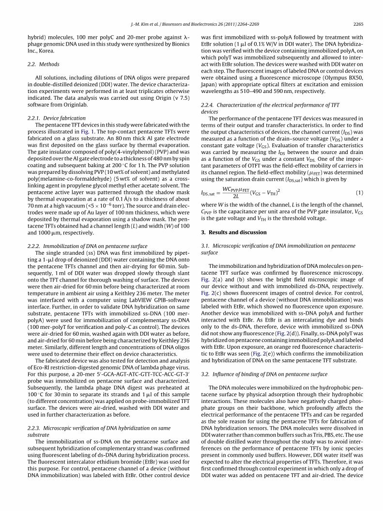
Bioele
hpI
2
itis
2
pfwTdcwplpb7tdta
2
ttsowtwisp(wamw
oFpS1(su
2s
suTtD
J.-M. Kim et al. / Biosensors and
ybrid) molecules, 100 mer polyC and 20-mer probe against �-hage genomic DNA used in this study were synthesized by Bionics
nc., Korea.
.2. Methods
All solutions, including dilutions of DNA oligos were preparedn double-distilled deionized (DDI) water. The device characteriza-ion experiments were performed in at least triplicates otherwisendicated. The data analysis was carried out using Origin (v 7.5)oftware from Originlab.
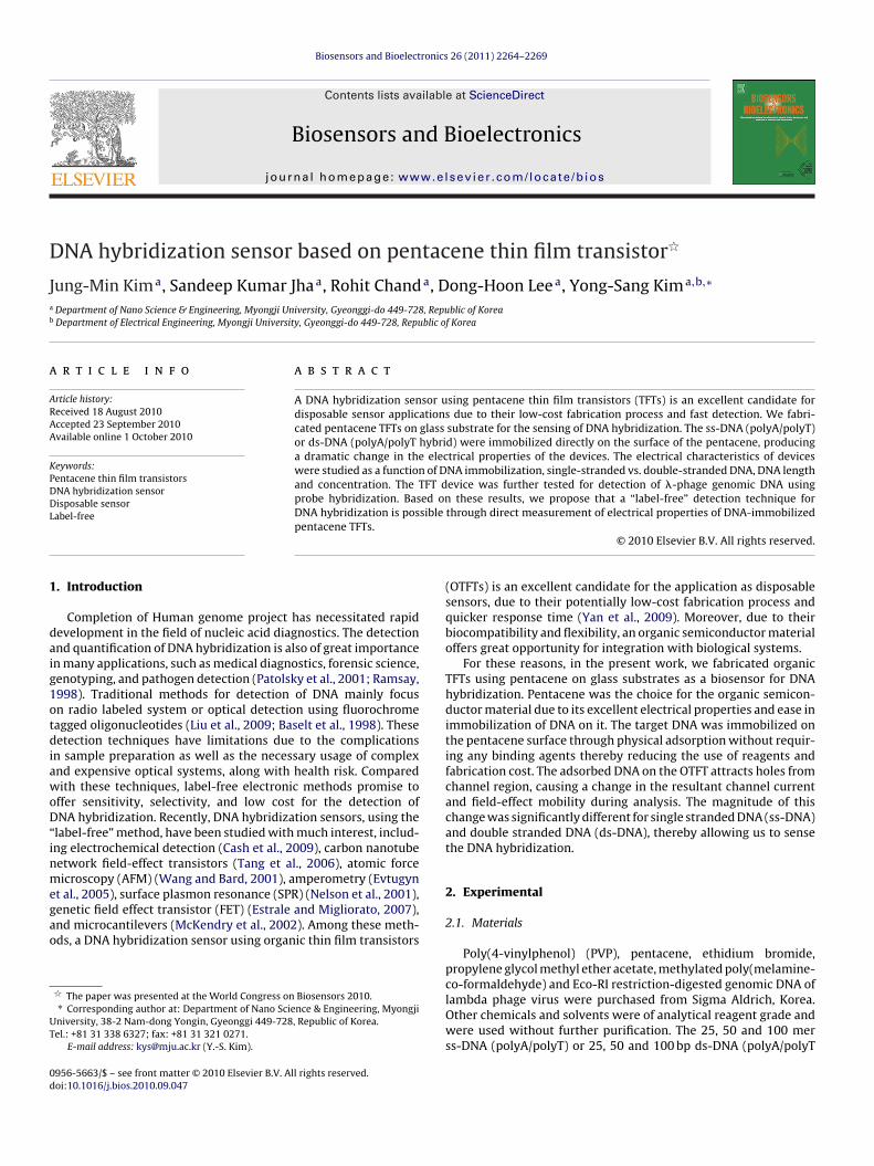
.2.1. Device fabricationThe pentacene TFT devices in this study were fabricated with the
rocess illustrated in Fig. 1. The top-contact pentacene TFTs wereabricated on a glass substrate. An 80 nm thick Al gate electrodeas first deposited on the glass surface by thermal evaporation.
he gate insulator composed of poly(4-vinylphenol) (PVP) and waseposited over the Al gate electrode to a thickness of 480 nm by spinoating and subsequent baking at 200 ◦C for 1 h. The PVP solutionas prepared by dissolving PVP (10 wt% of solvent) and methylatedoly(melamine-co-formaldehyde) (5 wt% of solvent) as a cross-
inking agent in propylene glycol methyl ether acetate solvent. Theentacene active layer was patterned through the shadow masky thermal evaporation at a rate of 0.1 A/s to a thickness of about0 nm at a high vacuum (<5 × 10⁻⁶ torr). The source and drain elec-rodes were made up of Au layer of 100 nm thickness, which wereeposited by thermal evaporation using a shadow mask. The pen-acene TFTs obtained had a channel length (L) and width (W) of 100nd 1000 �m, respectively.
.2.2. Immobilization of DNA on pentacene surfaceThe single stranded (ss) DNA was first immobilized by pipet-
ing a 1-�l drop of deionized (DDI) water containing the DNA ontohe pentacene TFTs channel and then air-drying for 60 min. Sub-equently, 1 ml of DDI water was dropped slowly through slantnto the TFT channel for thorough washing of surface. The devicesere then air-dried for 60 min before being characterized at room
emperature in ambient air using a Keithley 236 meter. The meteras interfaced with a computer using LabVIEW GPIB-software
nterface. Further, in order to validate DNA hybridization on sameubstrate, pentacene TFTs with immobilized ss-DNA (100 mer-olyA) were used for immobilization of complementary ss-DNA100 mer-polyT for verification and poly-C as control). The devicesere air-dried for 60 min, washed again with DDI water as before,
nd air-dried for 60 min before being characterized by Keithley 236eter. Similarly, different length and concentrations of DNA oligosere used to determine their effect on device characteristics.
The fabricated device was also tested for detection and analysisf Eco-RI restriction-digested genomic DNA of lambda phage virus.or this purpose, a 20-mer 5′-GCA-AGT-ATC-GTT-TCC-ACC-GT-3′
robe was immobilized on pentacene surface and characterized.ubsequently, the lambda phage DNA digest was preheated at00 ◦C for 30 min to separate its strands and 1 �l of this sampleto different concentration) was applied on probe-immobilized TFTurface. The devices were air-dried, washed with DDI water andsed in further characterization as before.
.2.3. Microscopic verification of DNA hybridization on sameubstrate
The immobilization of ss-DNA on the pentacene surface and
ubsequent hybridization of complementary strand was confirmedsing fluorescent labeling of ds-DNA during hybridization process.he fluorescent intercalator ethidium bromide (EtBr) was used forhis purpose. For control, pentacene channel of a device (withoutNA immobilization) was labeled with EtBr. Other control devicectronics 26 (2011) 2264–2269 2265
was first immobilized with ss-polyA followed by treatment withEtBr solution (1 �l of 0.1% W/V in DDI water). The DNA hybridiza-tion was verified with the device containing immobilized polyA, onwhich polyT was immobilized subsequently and allowed to inter-act with EtBr solution. The devices were washed with DDI water oneach step. The fluorescent images of labeled DNA or control deviceswere obtained using a fluorescence microscope (Olympus BX50,Japan) with appropriate optical filters at excitation and emissionwavelengths as 510–490 and 590 nm, respectively.
2.2.4. Characterization of the electrical performance of TFTdevices
The performance of the pentacene TFT devices was measured interms of their output and transfer characteristics. In order to findthe output characteristics of devices, the channel current (IDS) wasmeasured as a function of the drain–source voltage (VDS) under aconstant gate voltage (VGS). Evaluation of transfer characteristicswas carried by measuring the IDS between the source and drainas a function of the VGS under a constant VDS. One of the impor-tant parameters of OTFT was the field-effect mobility of carriers inits channel region. The field-effect mobility (�FET) was determinedusing the saturation drain current (IDS,sat) which is given by
IDS,sat = WCPVP�FET
2L(VGS − VTH)2 (1)
where W is the width of the channel, L is the length of the channel,CPVP is the capacitance per unit area of the PVP gate insulator, VGSis the gate voltage and VTH is the threshold voltage.
3. Results and discussion
3.1. Microscopic verification of DNA immobilization on pentacenesurface
The immobilization and hybridization of DNA molecules on pen-tacene TFT surface was confirmed by fluorescence microscopy.Fig. 2(a) and (b) shows the bright field microscopic image ofour device without and with immobilized ds-DNA, respectively.Fig. 2(c) shows fluorescent images of control device. For control,pentacene channel of a device (without DNA immobilization) waslabeled with EtBr, which showed no fluorescence upon exposure.Another device was immobilized with ss-DNA polyA and furtherinteracted with EtBr. As EtBr is an intercalating dye and bindsonly to the ds-DNA, therefore, device with immobilized ss-DNAdid not show any fluorescence (Fig. 2(d)). Finally, ss-DNA polyT washybridized on pentacene containing immobilized polyA and labeledwith EtBr. Upon exposure, an orange red fluorescence characteris-tic to EtBr was seen (Fig. 2(e)) which confirms the immobilizationand hybridization of DNA on the same pentacene TFT substrate.
3.2. Influence of binding of DNA on pentacene surface
The DNA molecules were immobilized on the hydrophobic pen-tacene surface by physical adsorption through their hydrophobicinteractions. These molecules also have negatively charged phos-phate groups on their backbone, which profoundly affects theelectrical performance of the pentacene TFTs and can be regardedas the sole reason for using the pentacene TFTs for fabrication ofDNA hybridization sensors. The DNA molecules were dissolved inDDI water rather than common buffers such as Tris, PBS, etc. The useof double distilled water throughout the study was to avoid inter-
ferences on the performance of pentacene TFTs by ionic speciespresent in commonly used buffers. However, DDI water itself wasexpected to alter the electrical properties of TFTs. Therefore, it wasfirst confirmed through control experiment in which only a drop ofDDI water was added on pentacene TFT and air-dried. The device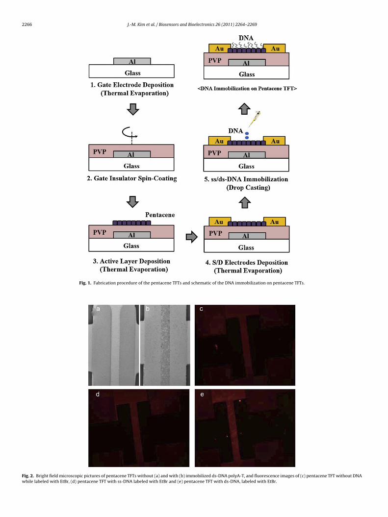
2266 J.-M. Kim et al. / Biosensors and Bioelectronics 26 (2011) 2264–2269
Fig. 1. Fabrication procedure of the pentacene TFTs and schematic of the DNA immobilization on pentacene TFTs.
Fig. 2. Bright field microscopic pictures of pentacene TFTs without (a) and with (b) immobilized ds-DNA polyA-T, and fluorescence images of (c) pentacene TFT without DNAwhile labeled with EtBr, (d) pentacene TFT with ss-DNA labeled with EtBr and (e) pentacene TFT with ds-DNA, labeled with EtBr.
J.-M. Kim et al. / Biosensors and Bioelectronics 26 (2011) 2264–2269 2267
Foi
sOcdoiitb
w1spttsTIVgpCaD
tacene TFTs. When the DNA molecules were immobilized on the
ig. 3. Performance of the pentacene TFTs with DNA immobilized on pentacene: (a)utput and (b) transfer characteristics of two pentacene TFTs (original, ss-DNA). Thenset of shows the DNA sensing mechanism on the pentacene TFTs.
howed no alteration in the electrical properties of pentacene TFTs.n the other hand, pentacene TFTs showed reductions in channelurrent and field-effect mobility while analyzing DNA immobilizedevices after rinsing with DDI water and air-drying for 1 h. More-ver, it is well known fact that adsorption of molecules on a surfaces controlled through temperature and is governed by Freundlichsotherm curve. Therefore, all the studies were carried out at roomemperature (25 ◦C in ambient air) to minimize variations in immo-ilization condition.
The influence of the immobilized DNA on pentacene surfacesas first studied by fabricating the pentacene TFTs with 100 mer,
00 pmol ss-DNA (polyA) for 60 min (immobilization time). Fig. 3(a)hows the IDS as a function of VDS under different VGS (the out-ut characteristic), whereas, Fig. 3(b) shows IDS as a function ofhe VGS measured at a constant VDS (the transfer characteris-ic). At the same applied VGS, original pentacene TFTs (withouts-DNA immobilization) showed higher IDS than for pentaceneFTs with immobilized ss-DNA. After immobilizing ss-DNA, the
DS of the device reduced approximately to 58.9% (at VDS = −30 V,GS = −30 V). The field-effect mobility in the pentacene TFTs asiven by Eq. (1) is influenced by the DNA molecules. Original
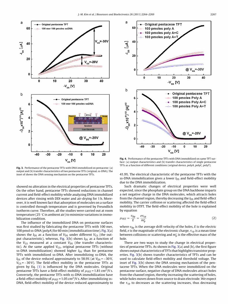
entacene TFTs have a field-effect mobility of �FET = 1.81 cm2/V s.onversely, the pentacene TFTs with ss-DNA immobilization havefield-effect mobility of �FET = 1.05 cm2/V s. After immobilizing ss-NA, field-effect mobility of the device reduced approximately toFig. 4. Performance of the pentacene TFTs with DNA immobilized on same TFT sur-face: (a) output characteristics and (b) transfer characteristics of single pentaceneTFTs as a function of different conditions (original device, polyA, polyC, polyT).
41.9%. The electrical characteristic of the pentacene TFTs with thess-DNA immobilization gives a lower IDS and field-effect mobilitydue to the DNA immobilization.
Such dramatic changes of electrical properties were wellexpected, since the phosphate group on the DNA backbone impartsa net negative charge in the DNA molecules, which attracts holesfrom the channel region, thereby decreasing the IDS and field-effectmobility. The carrier collision or scattering affected the field-effectmobility in OTFT. The field-effect mobility of the hole is explainedby equation
�FET = vdp
E= e�cp
m∗p
(2)
where vdp is the average drift velocity of the holes, E is the electricfield, e is the magnitude of the electronic charge, �cp is a mean timebetween collisions or scattering and m∗
p is the effective mass of thehole.
There are two ways to study the change in electrical proper-ties of pentacene TFTs. As shown in Fig. 3(a) and (b), the first figureshows output characteristics of TFTs that highlights transistor prop-erties. Fig. 3(b) shows transfer characteristics of TFTs and can beused to calculate field-effect mobility and threshold voltage. Theinset of Fig. 3(b) shows the DNA sensing mechanism of the pen-
pentacene surface, negative charge of DNA molecules attract holesfrom the channel region, thereby increasing the scattering of holes,while holes moves down from source to drain electrode. We expectthe �cp to decreases as the scattering increases, thus decreasing

2268 J.-M. Kim et al. / Biosensors and Bioelectronics 26 (2011) 2264–2269
FTc
fiTfitbap
p1tttitVtatttf
11
Fig. 6. Performance of the pentacene TFTs with single stranded 20-mer probe immo-bilized on pentacene surface and upon hybridization of �-phage DNA. (a) Output
ig. 5. Reduction ratio of channel current and field-effect mobility for the pentaceneFTs with immobilized ss-DNA, with respect to original device, as a function of DNAoncentration (a) and DNA length (b).
eld-effect mobility as calculated by Eq. (2). The IDS of pentaceneFTs as given by Eq. (1) is influenced by the DNA molecules. Theeld-effect mobility decreases as the scattering of holes increases,hereby decreasing IDS. This observation contradicts previous claimy Zang and Subramanian (2007) where the investigators reportedn increase in IDS level, which was a misinterpretation of currenthenomena as we can show on the basis of present results.
Additionally, we also found a dramatic difference in the IDS andattern in field-effect mobility upon exposure to either 100 mer,00 pmol ss-DNA or ds-DNA at same pentacene TFT. Fig. 4 showshe difference in the sensor output and the transfer characteris-ics from the original pentacene TFT (without ss-DNA) comparedo the pentacene TFT with immobilized ss-DNA or ds-DNA. Aftermmobilizing ds-DNA, the IDS of the device reduced approximatelyo 86.55% compared with that of original device (at VDS = −30 V,GS = −30 V) which was more than that for ss-DNA (58.9%). In addi-ion, the field-effect mobility reduced to 41.9 and 84.41% for ss-DNAnd ds-DNA, respectively. This enables the direct electrical detec-ion of the DNA hybridization through the measurement of IDS forhe pentacene TFTs. The net difference in the IDS (�IDS) on the pen-acene TFTs due to the single or double stranded DNA was the basis
or the analysis of the DNA hybridization.To confirm the DNA hybridization on single pentacene TFT,00 pmol of 100 mer polyC was dropped on the polyA (100 mer,00 pmol) immobilized pentacene TFT. In this device, polyC did
characteristics and (b) transfer characteristics of three pentacene TFTs (original,ss-DNA, hybridized �-phage DNA).
not immobilize on pentacene channel layer as polyA was alreadyimmobilized on this surface. Also, as expected, polyC did nothybridize to polyA. As a result, there was no significant alterationin the electrical properties of pentacene TFT (Fig. 4). On the otherhand, the TFT device showed significant change in electrical proper-ties due to hybridization by same concentration of polyT over polyA(Fig. 4). This result indicates the possibility of selective responsefrom devices having different DNA molecules immobilized on pen-tacene.
In order to derive any correlation between the device responseand the extent of the DNA concentration, the output and transfercharacteristics of the devices were also measured by varying theconcentration of the ss-DNA on the pentacene surface (Fig. 5(a)). AsDNA concentration was increased, the IDS value decreased approxi-mately to 47.36, 59.31 and 80.35%, respectively and so a decrease inthe field-effect mobility was observed which were approximately38.06, 53.32 and 79.31%, respectively for 50, 100 and 200 pmol of50-mer ss-DNA. Such a reduction in IDS and field-effect mobilitywas due to the increase in the concentration of immobilized DNA onthe pentacene surface, which collectively attracts more holes from
the channel region. This result indicates the possibility of dynamicresponse from devices having low concentration of DNA immobi-lized on pentacene and enable estimation of DNA concentrationupon hybridization.
Bioele
atbswcdaaain
po2Pisfisshwsptol
4
l
J.-M. Kim et al. / Biosensors and
As the length of ss-DNA immobilized on pentacene surface islso expected to influence the device properties, the output andransfer characteristics of the devices were measured while immo-ilizing varying length of ss-DNA on the pentacene surface. Fig. 5(b)hows the influence of the DNA length on pentacene surface, whichas studied with 25, 50 and 100 mer ss-DNA of the same con-
entration (50 pmol). As DNA length was increased, the IDS valueecreased approximately to 34.8, 47.36 and 56.99% respectivelynd so a decrease in the field-effect mobility was observed topproximately 14.35, 38.06 and 50% level, respectively for 25, 50nd 100 mer DNA. Such a reduction in IDS and field-effect mobil-ty was due to the fact that longer DNA length carries more netegative charge.
Finally, as a proof of concept, we attempted to detect bacterio-hage lambda through hybridization of genomic DNA of the virusver a probe-immobilized pentacene TFT device. For this purpose, a0-mer probe 5′-GCA-AGT-ATC-GTT-TCC-ACC-GT-3′ similar to theCR primer used for amplification of organism’s genomic DNA wasmmobilized on pentacene surface and characterized (Fig. 6). Sub-equently, the lambda phage DNA digest was preheated at 100 ◦Cor 30 min to separate its strands and 1 �l of this sample (contain-ng 1 �g and 100 ng DNA) was applied on probe-immobilized TFTurface. Restriction digestion of lambda phage DNA ensured fivemaller fragments of ds-DNA for ease in separating the strands andybridization over its probe. The devices were air-dried, washedith DDI water and used in further characterization as before. As
een from Fig. 6, the device showed significant change in electricalroperties on response to different concentrations of complemen-ary DNA from �-phage. This result demonstrates the feasibility ofur device as a disposable sensor for DNA hybridization and canead to development of biosensor for rapid pathogen detection.
. Conclusion
The single and double stranded DNA molecules were immobi-ized on the surface of the pentacene layer, producing a change
ctronics 26 (2011) 2264–2269 2269
in the performance of the pentacene TFTs. It is attributable to thenegative charges on the DNA molecules having the ability to attractholes from the channel region. The electrical characteristic of thepentacene TFTs with the ds-DNA immobilization gives a lower cur-rent output and field-effect mobility compared to ss-DNA sincethe ds-DNA carry more net negative charge. Therefore, we pro-pose, in conclusion, that a “label-free” detection technique for DNAhybridization with high sensitivity and selectivity is possible torealize portable and disposable DNA sensor having application inmolecular biology laboratories, medical diagnostics, forensic inves-tigations, genotyping, pathogen detection and so on.
Acknowledgement
This work was supported by Grant no. (ROA-2006-000-10274-0) from the National Research Laboratory Program of the KoreaScience & Engineering Foundation.
References
Baselt, D.R., Lee, G.U., Natesan, M., Metzger, S.W., Sheehan, P.E., Colton, R.J., 1998.Biosens. Bioelectron. 13, 731–739.
Cash, K.J., Heeger, A.J., Plaxco, K.W., Xiao, Y., 2009. Anal. Chem. 81, 656–661.Estrale, P., Migliorato, P., 2007. J. Mater. Chem. 17, 219–224.Evtugyn, G.A., Goldfarb, O.E., Budnikov, H.C., Ivanov, A.N., Vinter, V.G., 2005. Sensors
5, 364–376.Liu, J., Cao, Z., Lu, Y., 2009. Chem. Rev. 109, 1948–1998.McKendry, R., Zhang, J.Y., Arntz, Y., Strunz, T., Hegner, M., Lang, H.P., Baller, M.K.,
Certa, U., Meyer, E., Guntherodt, H.J., Gerber, C., 2002. Proc. Natl. Acad. Sci. U.S.A.99, 9783–9788.
Nelson, B.P., Grimsrud, T.E., Liles, M.R., Goodman, R.M., Corn, R.M., 2001. Anal. Chem.73, 1–7.
Patolsky, F., Lichtenstein, A., Willner, I., 2001. Nat. Biotechnol. 19, 253–257.Ramsay, G., 1998. Nat. Biotechnol. 16, 40–44.
Tang, X., Bansaruntip, S., Nakayama, N., Yenilmez, E., Chang, Y.L., Wang, Q., 2006.Nano Lett. 6, 1632–1636.Wang, J., Bard, A., 2001. J. Anal. Chem. 73, 2207–2212.Yan, F., Mok, S.M., Yu, J., Chan, H.L.W., Yang, M., 2009. Biosens. Bioelectron. 24,
1241–1245.Zang, Q.T., Subramanian, V., 2007. Biosens. Bioelectron. 22, 3182–3187.