development of a batch fabrication process for chemical ... · development of a batch fabrication...
TRANSCRIPT
National Aeronautics and Space Administration
www.nasa.gov
Development of a Batch Fabrication Process for Chemical Nanosensors:
Recent Advancements at NASA Glenn Research Center
Dr. Azlin M. Biaggi-Labiosa
NASA Glenn Research Center
Email: [email protected]
http://www.grc.nasa.gov/WWW/sensors/

National Aeronautics and Space Administration
www.nasa.govCommunications and Intelligent Systems DivisionSmart Sensors and Electronics Systems Branch
OUTLINE
• Background
• Previous Work
• Experimental
• Results and Discussion
• Summary
• Acknowledgements
2

National Aeronautics and Space Administration
www.nasa.gov 3
Nanocrystalline Tin
Oxide NOx and CO
Sensor
Oxygen Sensor
H2 Sensor
SiC Hydrocarbon Sensor
“Lick and Stick” Space Launch Vehicle Leak Sensors with Power and Telemetry
Sensor EquippedPrototype Medical
Pulmonary Monitor
Aircraft Propulsion Exhaust High Temperature Electronic Nose
Multi Species Fire Sensors for Aircraft Cargo Bays and Space Applications
Hydrazine EVA Sensors
(ppb Level Detection)
Environmental monitoring(ISS Whitesand Testing)
Integration of Micro Sensor Combinations into Small, Rugged Sensor Suites
Example Applications: AEROSPACE VEHICLE FIRE, FUEL LEAKS, EMISSIONS,
ENVIRONMENTAL MONITORING, CREW HEALTH, SECURITY
National Aeronautics and Space Administration
www.nasa.govCommunications and Intelligent Systems DivisionSmart Sensors and Electronics Systems Branch
BACKGROUND
• Fabrication of operational sensors from nanostructures is less mature than MEMS sensors.
• No matter how good the sensor, if you cannot make contact with the sensor, then the device will be ineffective.
• Micro-nano integration/contacts
– Major question for nanostructured based sensors: how are the nanostructured materials integrated into a micro/macro structure
• Cost effectiveness, time-efficient, controlled electrical contact
• Typical standard method of deposition of nanostructures onto a sensor platform
– Disperse in suspension and deposit on a substrate
• Simple but difficult to reproduce
• Inability to mass produce sensors in a controllable way.
4
National Aeronautics and Space Administration
www.nasa.govCommunications and Intelligent Systems DivisionSmart Sensors and Electronics Systems Branch
BACKGROUND
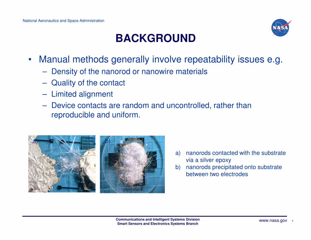
• Manual methods generally involve repeatability issues e.g.
– Density of the nanorod or nanowire materials
– Quality of the contact
– Limited alignment
– Device contacts are random and uncontrolled, rather than reproducible and uniform.
5
a) b)
a) nanorods contacted with the substrate via a silver epoxy
b) nanorods precipitated onto substrate between two electrodes
National Aeronautics and Space Administration
www.nasa.govCommunications and Intelligent Systems DivisionSmart Sensors and Electronics Systems Branch
BACKGROUND
• Attempts to control orientation and alignment ofnanostructures on microdevices:
– AFM or laser tweezers
• Labor-intensive
• Not viable for mass production
– e-beam lithography
• High-end processing
• Limited to nanodimensional linewidths (standard microfabricationtechniques require larger linewidth resolutions)
– Langmuir-Blodgett method
• Slow compression of dispersed nanostructures in organic solution onsubstrate until desired structure is achieved.
• Range of materials is limited
– Superlattice nanowire pattern transfer (SNAP)
• Range of materials is limited.
6
National Aeronautics and Space Administration
www.nasa.govCommunications and Intelligent Systems DivisionSmart Sensors and Electronics Systems Branch
PREVIOUS WORK
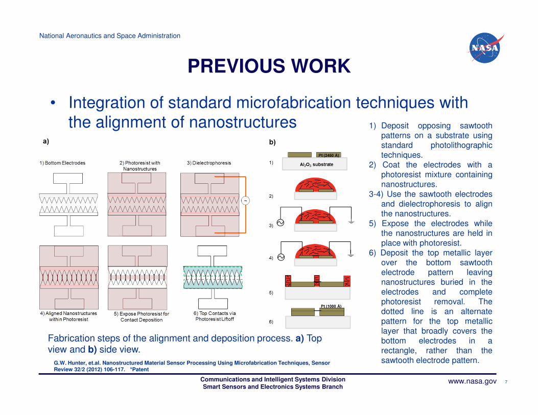
• Integration of standard microfabrication techniques with the alignment of nanostructures
7
1) Deposit opposing sawtoothpatterns on a substrate usingstandard photolithographictechniques.
2) Coat the electrodes with aphotoresist mixture containingnanostructures.
3-4) Use the sawtooth electrodesand dielectrophoresis to alignthe nanostructures.
5) Expose the electrodes whilethe nanostructures are held inplace with photoresist.
6) Deposit the top metallic layerover the bottom sawtoothelectrode pattern leavingnanostructures buried in theelectrodes and completephotoresist removal. Thedotted line is an alternatepattern for the top metalliclayer that broadly covers thebottom electrodes in arectangle, rather than thesawtooth electrode pattern.
Fabrication steps of the alignment and deposition process. a) Top view and b) side view.
G.W. Hunter, et.al. Nanostructured Material Sensor Processing Using Microfabrication Techniques, Sensor Review 32/2 (2012) 106-117. *Patent
National Aeronautics and Space Administration
www.nasa.govCommunications and Intelligent Systems DivisionSmart Sensors and Electronics Systems Branch
PREVIOUS WORK
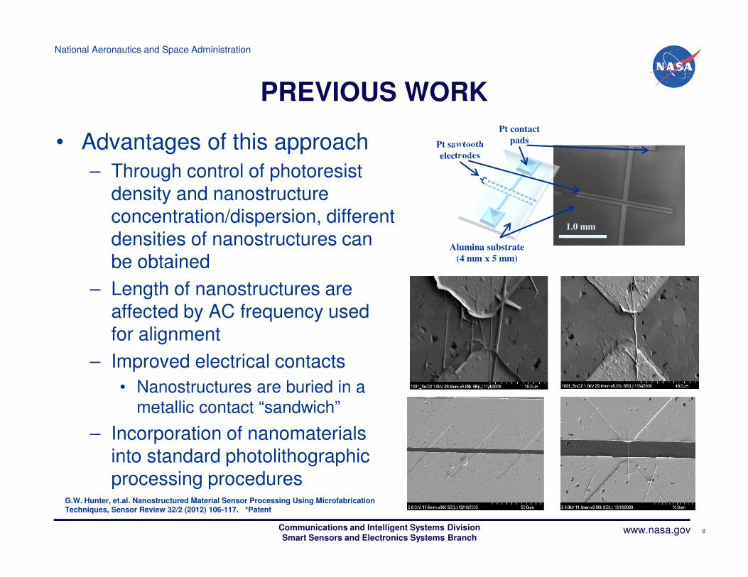
• Advantages of this approach
– Through control of photoresist density and nanostructure concentration/dispersion, different densities of nanostructures can be obtained
– Length of nanostructures are affected by AC frequency used for alignment
– Improved electrical contacts
• Nanostructures are buried in a metallic contact “sandwich”
– Incorporation of nanomaterials into standard photolithographic processing procedures
8
1.0 mm
Pt sawtooth
electrodes
Pt contact
pads
Alumina substrate
(4 mm x 5 mm)
G.W. Hunter, et.al. Nanostructured Material Sensor Processing Using Microfabrication Techniques, Sensor Review 32/2 (2012) 106-117. *Patent

National Aeronautics and Space Administration
www.nasa.govCommunications and Intelligent Systems DivisionSmart Sensors and Electronics Systems Branch
PREVIOUS WORK
• Motivation:
– Build a SnO2-based sensor for H2 and hydrocarbons that can operate at room temperature as well as high temperatures.
– SnO2 is an n-type wide band gap (~3.6 eV) semiconductor.
– Sensors usually operate above 200°C due to their reactionmechanism.
9
(a) Adsorption of oxygen at the surface creates
surface-acceptor sites that immobilize
conduction band electrons from the near
surface region, creating a depletion layer.
(b) Reducing gases, such as CO, remove
surface bound oxygen atoms, releasing the
immobilized electrons, reducing the
thickness of the depletion layer.
Schematic representation of the reactions occurring at the surface of an n-type
semiconductor metal oxide

National Aeronautics and Space Administration
www.nasa.govCommunications and Intelligent Systems DivisionSmart Sensors and Electronics Systems Branch
PREVIOUS WORK
10
• The shaded part shows the core region
and the unshaded part shows the
depletion layer and GB = grain
boundary.
• a) D >> 2L, the conductance, which is
higher in the non-depleted core region,
is controlled by grain boundaries.
• b) D ≈ 2L, where necks between
coalesced primary grains control the
conductance.
• c) D < 2L, when the grains are small
enough to be fully depleted the
conductance is grain controlled [4]
A. Rothschild and Y. Komen. The effect of grain size on the sensitivity of nanocrystallinemetal-oxide gas sensors, J. App. Phys. 95, 6374 (2004).
Three mechanisms of conductance in metal-oxide gas sensitive materials:
When the SnO2 crystallite size is
comparable with or less than 2L (~ 6
nm), where L is the depth of the space-
charge layer, the sensitivity can be
greatly increased.
National Aeronautics and Space Administration
www.nasa.govCommunications and Intelligent Systems DivisionSmart Sensors and Electronics Systems Branch
PREVIOUS WORK
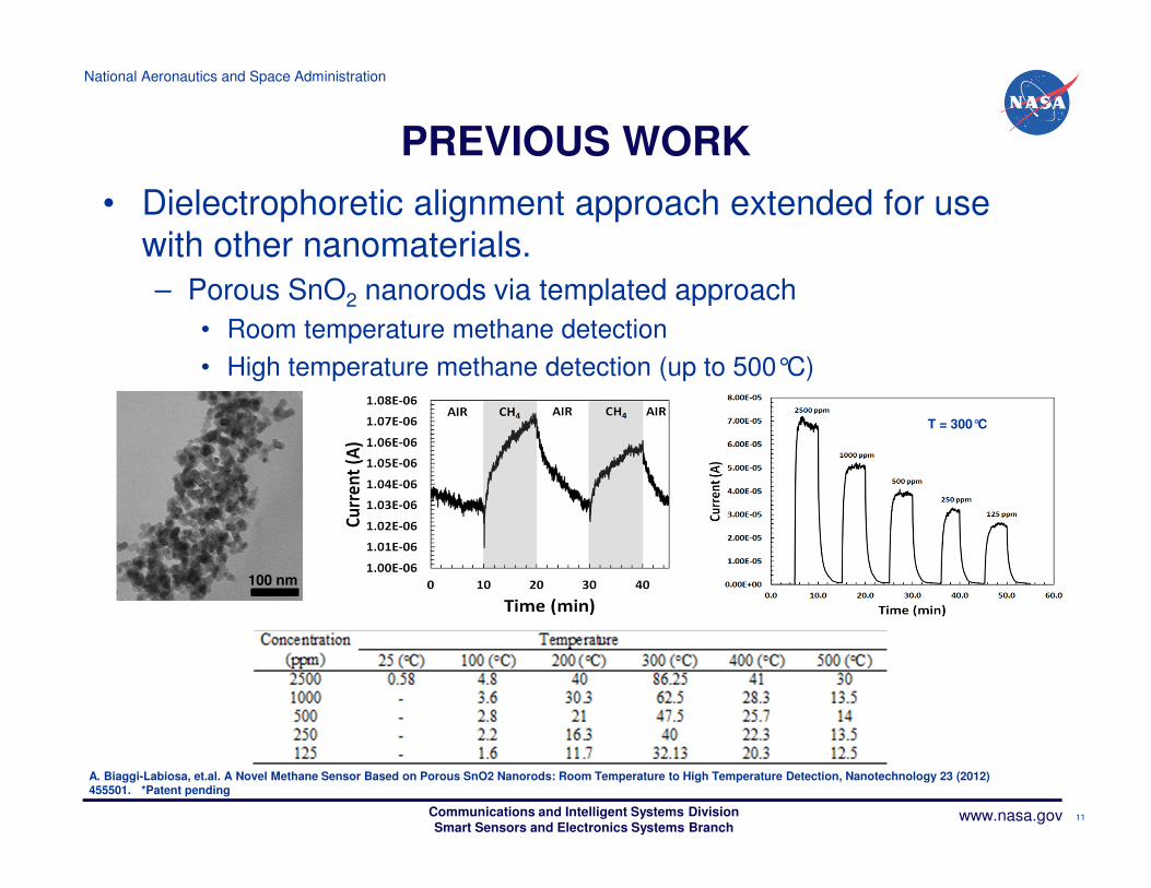
• Dielectrophoretic alignment approach extended for use with other nanomaterials.
– Porous SnO2 nanorods via templated approach
• Room temperature methane detection
• High temperature methane detection (up to 500°C)
11
100 nm
T = 300°C
A. Biaggi-Labiosa, et.al. A Novel Methane Sensor Based on Porous SnO2 Nanorods: Room Temperature to High Temperature Detection, Nanotechnology 23 (2012) 455501. *Patent pending
National Aeronautics and Space Administration
www.nasa.govCommunications and Intelligent Systems DivisionSmart Sensors and Electronics Systems Branch
EXPERIMENTAL
• Goal: Mass production of sensors with uniformly controlled properties.
– Broader applications
• Commercial MWCNTs (NanoLab) were used for the proof-of-concept.
– Diameter 15±5 nm
– Length 5-20 µm
– S1805 photoresist solution concentration 2 mg/mL
• Array of paired patterned Pt electrodes on a 2” alumina wafer.
– Electrical connection in such a way that a field applied to one set of electrodes is simultaneously applied to the full array on the wafer.
– Distance between opposing sawtooth electrodes ~1-2 µm
– 20 MHz, 10 Vp-p, 0 Voffset for 20 min
12

National Aeronautics and Space Administration
www.nasa.govCommunications and Intelligent Systems DivisionSmart Sensors and Electronics Systems Branch
RESULTS AND DISCUSSION
• Design
– There are 16 patterns, each with 146 opposing sawtooth electrodes for a total of 2336 electrodes.
– Can be separated into individual sensors.
13
2
6
4
8
10
12
14
20
30
40
Probe contact
Probe contact

National Aeronautics and Space Administration
www.nasa.govCommunications and Intelligent Systems DivisionSmart Sensors and Electronics Systems Branch
RESULTS AND DISCUSSION
• Proof-of-concept
– SEM images of aligned MWCNTs on the whole wafer
14
a) Lower magnification to show
alignment on more than one
sawtooth electrode.
b) Alignment of a few nanotubes
between opposing electrodes.
c) Alignment of more nanotubes
between opposing electrodes.
d) Image of alumina substrate
showing that there are no
nanotubes (or a little amount)
demonstrating that the nanotubes
are found between opposing
electrodes.
Managed to obtain alignment on 2313 of the2336 electrodes for a 99% yield.
National Aeronautics and Space Administration
www.nasa.govCommunications and Intelligent Systems DivisionSmart Sensors and Electronics Systems Branch
SUMMARY
• Standardized approach to chemical sensors processing using nanostructures.
– Integration and alignment of nanostructures with microfabrication methods.
• Mass production of sensors with uniformly controlled properties.
• Approach addresses significant barriers in integrating nanotechnology with microsensors, such as
– Deposition control
– Contact robustness
– Simplified processing
15

National Aeronautics and Space Administration
www.nasa.govCommunications and Intelligent Systems DivisionSmart Sensors and Electronics Systems Branch
SUMMARY
• Resulting sensors can be used in applications where presently microsensors are used.
• Further refinement of the DEP and photoresist suspension are planned to increase and to better control the yield for each paired contact pattern.
• Current work in applying mass production approach with metal oxide nanostructures.
16
National Aeronautics and Space Administration
www.nasa.govCommunications and Intelligent Systems DivisionSmart Sensors and Electronics Systems Branch
ACKNOWLEDGEMNTS
• Dr. Gary Hunter, Laura Evans, Gordon Berger andDr. Jennifer Xu
• Technical Support:
― José M. González
― Michelle Mrdenovich
― Christopher Hampton
• Dr. Lawrence G. Matus and Dr. Mary V. Zeller forhelpful discussions.
• Research supported by the Vehicle Systems SafetyTechnologies (VSST) Project.
17

National Aeronautics and Space Administration
www.nasa.govCommunications and Intelligent Systems DivisionSmart Sensors and Electronics Systems Branch
QUESTIONS
18