designand applications q passivedevices multi-layered...
TRANSCRIPT
Design and Applications of High Q Passive Devices
on Multi-Layered Liquid Crystalline PolymerBased Substrates for Handset Applications
Amit Bavisi, Wansuk Yun, Venky Sundaram, and Madhavan Swaminathan
School of Electrical and Computer Engineering, Georgia Institute of Technology, Atlanta, Georgia 30332
Abstract- In the recent past, fully packaged RF modulessuitable for integration in wireless handsets have been fabricatedon organic packaging technology that uses a single sheet LiquidCrystalline Polymer (LCP) substrate. This paper demonstratesthe RF characterization of inductors that were fabricated on twodifferent stack-ups utilizing different configurations of the LCPsubstrate. The paper, then, shows the implementations of theembedded LC passives in RF front-end modules such as voltagecontrolled oscillators (VCOs) and tunable filters. The firstapplication is the design and implementation of a 1.8 GHzfeedback oscillator in a novel multi-layer laminate-type processtechnology that uses three layers of LCP substrate. Themicrostrip type oscillator measures a phase noise of -117 dBc/Hzat 100 KHz offset at 10 mW of power consumption. The oscillatormeets the stringent phase noise specifications of cellular systemsfor both mobile-station and base-stations. The final application ofthe high quality factor (Q) passives is in the design andimplementation of voltage tunable filters useful for WLANapplications. The filters were fabricated on a completely differentstack-up that uses two layers of LCP substrate. The filterprototype is tunable from 1.75 to 2.03 GHz with an insertion lossof 2.5 dB using lossy surface-mount varactor diodes.
I. INTRODUCTION
Recent developments in the Liquid Crystalline Polymer(LCP) based processing technology have made LCP apromising technology for reliable system-in-package (SiP)applications at RF and microwave frequencies [ 1], [2].Electrical characteristics such as (a) low and stable dielectricconstant (£r = 2.95) and low loss (tan 6 = 0.002) uptomicrowave frequencies, and (b) low moisture absorption fordimensional stability [2] and high temperature tolerance makeit usable in harsh environments. The entire process is done at alow temperature and is compatible with standard printedwiring board infrastructure [2]. Additionally, it is a largepanel-area fabrication process (12" x 18") and has themechanical strength to be the final printed circuit board(PCB). Both manufacturing and electrical merits, as will bepresented in this paper, lead to a reduction in themanufacturing cost per component; thereby, making thetechnology useful for commercial RF applications. At mid-RFfrequencies (- 6 GHz), embedded capacitors with Qs in therange of 200-300 and inductors with Qs greater than 50 can bedesigned in LCP [2]. Because of the embedded nature of thecapacitors (Cs) and inductors (Ls), their characteristics can becontrolled over a large frequency range. The above mentioned
characteristics make LCP a feasible alternative to surfacemount Ls and Cs, as the solution will become completelyembedded. Unlike LTCC, components on LCP can beintegrated into the inner layers of a PCB. Hence, integrationusing LCP improves reliability and reduces mounting costs.The above stated characteristics make LCP an excellentcandidate for applications such as integrated filters [2],diplexers, duplexers, baluns, multiplexers, low noise amplifiers(LNAs) and VCOs [1],[3]. Present implementations of LCPbased passive and active modules are mostly planar and useonly one LCP sheet, which is bonded to multiple lower meltadhesives. But multi-band portable handsets require higherlevel of integrations for heavy signal routing, RF-digitalisolation, and form-factor reduction. Furthermore, currenttrend in the volume reduction of portable phones has placedadditional restrictions on the PCB thickness. The abovementioned restrictions map to a high Q process technology thatcan support large numbers of metal layers (- 10) and at thesame time have a low overall thickness (height).
This paper demonstrates novel, multiple cross-sections ofstacked-LCP based packaging technologies. Depending on theapplication requirements the position and the number of LCPsheets is changed. Fully-packaged modules such as a VCO andtunable filters are then demonstrated. In particular, this paperpresents a 10 mW, 1.8 GHz VCO on a three-LCP layer (6metal layers) process, suitable for cellular applications.Additionally, this paper shows the first implementation oftunable filters on LCP substrate. The filters were fabricated ona two-LCP layer (8 metal layers) process and were tuned usingcommercially available silicon varactor diodes. The effect oflossy varactor diodes on the LCP based filters is studied.
This paper is organized as follows: Section II shows themeasured Qs of the Ls on the proposed technologies. SectionIII shows the measurement results of the fully-packaged, novelVCO that is fabricated in a volume of 5.5 x 4.8 x 0.7 mm3.Section IV summarizes the measured results of the tunablefilter and discusses the effect of the lossy varactors on LCPbased filters. Finally, the conclusions are made in section V.
II. NOVEL LCP BASED PROCESS TECHNOLOGIES
Upto 10 GHz, lumped-element inductors and capacitors aretypically suitable for the design of RF front-end modules. Animprovement in the VCO and filter design methodology, in
0-7803-9433-X/05/$20.00 02005 IEEE. APMC2005 Proceedings
addition to size reduction, can be attained by moving fromtransmission line to lumped-element high Q inductors [1], [2].Many design methods, (a) line or slab inductors, (b) multiplelayer spiral inductors, and (c) patterned ground plane to namea few, have been employed for the optimization of the Qs ofthe inductors. In silicon, the metal loss and the substrate lossare the major contributors to the losses in an inductor, whichconstrains the design of oscillators and filters. Additionally,cellular base-stations impose severe temperature and reliabilityrequirements, where silicon based solutions fail. This sectionpresents two, LCP based process technologies and themeasured results of the high Q spiral inductors.
1) P-PIC Process Technology
Micro-vias Thsr-hole
|r MI-M2
LC -* ____ _ M3-M4
Core M5-M6
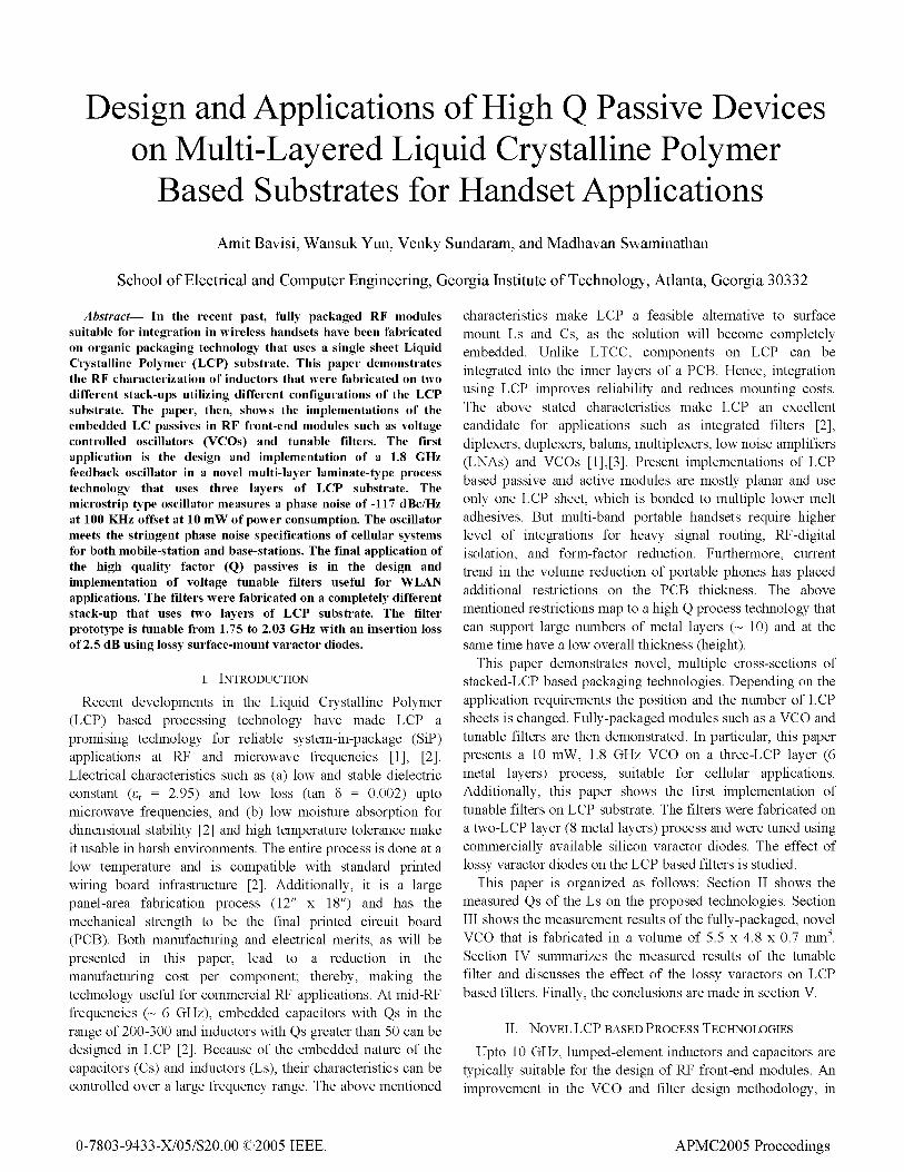
Fig. 1. Cross-section of the P-PIC process technology.
Fig. 1 shows the cross-section of the LCP based packagingtechnology that is suitable for both integration in both cellularhandsets and base-stations. Called Plastic-packaged IntegratedCircuitry (P-PIC), the stack-up consists of three, one mil thickLCP sheets that are bonded together by a lower melt adhesive.In total there are six metal layers and the total height of thestack-up is 0.7 mm. The LCP dielectric layer has a dielectricconstant of 2.95 and a loss tangent of 0.002. The adhesivelayer has a loss tangent of 0.0035. The low loss tangent andthick metal results in high Q inductors and high Q capacitors.High density inter-metal micro-vias with diameters < 100 pimcan be formed with high yield. The metal layers on the top andbottom of the LCP sheets were connected through micro-vias.The ability to form micro-vias is essential for high componentdensity and for high routing density. Additionally, lowresistance through-holes were employed for connection withthe bottom metal layer. P-PIC is a large area process, 12"x18",and hence, provides a means to manufacture large volume ofcomponents. A microstrip inductor designed on the metallayers MI and M2 is separated from the ground layer (M6) byatleast 0.7 mm and hence, enables the design of inductors withQs > 150. Additionally, M5 and M6 can be used to make largede-coupling capacitors for active circuits.
2) Balanced LCP Process TechnologyA variant of the above shown technology is a more balanced
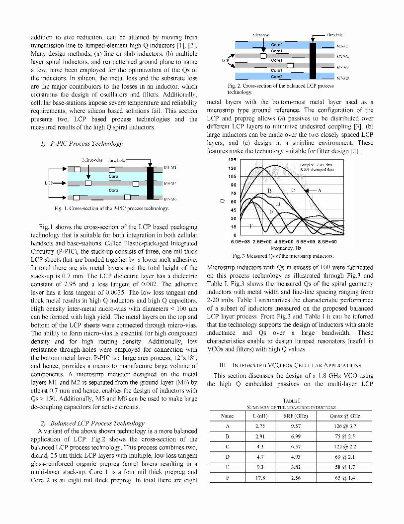
application of LCP. Fig.2 shows the cross-section of thebalanced LCP process technology. This process combines two,diclad, 25 um thick LCP layers with multiple, low loss tangentglass-reinforced organic prepreg (core) layers resulting in a
multi-layer stack-up. Core 1 is a four mil thick prepreg andCore 2 is an eight mil thick prepreg. In total there are eight
-4 Core2Corel
LCP Corel_~~~~~~~'l _
Corel _Ce _____
MI-M2
M3-M4
M5-M6
M7-M8
Fig. 2. Cross-section of the balanced LCP processtechnology.
metal layers with the bottom-most metal layer used as amicrostrip type ground reference. The configuration of theLCP and prepreg allows (a) passives to be distributed overdifferent LCP layers to minimize undesired coupling [3], (b)large inductors can be made over the two closely spaced LCPlayers, and (c) design in a stripline environment. Thesefeatures make the technology suitable for filter design [2].
135Sampled: VNA data
120 Solid: Averaged data
90 ____X_\75 ____
15
90
5.OE+08 2.5E+09 4.5E+09 6.5E+09 8.5E+09Frequency, Hz
Fig. 3 Measured Qs of the microstrip inductors.
Microstrip inductors with Qs in excess of 100 were fabricatedon this process technology as illustrated through Fig.3 andTable I. Fig.3 shows the measured Qs of the spiral geometryinductors with metal width and line-line spacing ranging from2-20 mils. Table I summarizes the characteristic performanceof a subset of inductors measured on the proposed balancedLCP layer process. From Fig.3 and Table I it can be inferredthat the technology supports the design of inductors with stableinductance and Qs over a large bandwidth. Thesecharacteristics enable to design lumped resonators (useful inVCOs and filters) with high Q values.
III. INTEGRATED VCO FOR CELLULAR APPLICATIONS
This section discusses the design of a 1.8 GHz VCO usingthe high Q embedded passives on the multi-layer LCP
TABLE ISUMMARY OF THE MEASURED INDUCTORS
Name L (nH) SRF (GHz) Qmax @ GHz
A2.75 9.57 126 @ 3.7
B 2.91 6.99 75 @ 2.5
C 4.3 6.57 122 @ 2.2
D 4.7 4.93 [email protected]
E 3e Q9.3 3.82 58m i1.7
F 17.8 2.56 65s 1.4
Micro-vias IqV- Thru-hole

substrate as shown in Fig. 1. The stack-up is attractive for VCOapplication due to (a) the stack-up separates the resonatorinductor from the ground and hence, minimizes thedegradation of the inductor Q that happens due to the closeproximity to ground, and (b) the presence of micro-vias in thetop LCP layer simplifies signal, dc, and inter componentrouting. In the case of feedback oscillators the phase noise isinversely proportional to the square of the resonator Q and tothe dc power consumption (from Leeson's formula [4]). From[4] it can be concluded that higher Qs of the resonator willlead to lower phase noise at low power levels.
A. VCO Design
Ci
Vo
RE A network
Fig. 4. Schematic of the fabricated feedback oscillator. L and Ciare feedback elements.
Fig.4 shows the schematic of the 1.8 GHz VCO. The proposedoscillator utilizes the concept of capacitive feedback from thebase terminal to the collector terminal of the transistor with theresonator inductor at the collector. Since the feedback isthrough a capacitive-divider network the circuit functioningresembles a Colpitt's oscillator [1]. The oscillator works on a
concept similar to a Colpitt's oscillator, as shown in [1], withan exception that in the present case the feedback is from thecollector terminal to the base of the transistor. Hence, theresonator is loaded by the high input impedance of the emitter-degenerated transistor, on one side, and by the high collector-resistance of the transistor on the other side. As a result, thedegradation of phase noise due to resonator loading is avoided,which is present in the Colpitt's oscillator [1].
B. Experimental ResultsCarrier Power 0 dBrm Atten 0.00 dB MWr 100.000 kHzRef -9000dBc/H, -1 16.73 dBc/Hz
I X AK SS 1 g2L1B01L
10 kHz Frequencg Offset 10 MHz~~~~~~~~~~~~~~.
(a) (b)Fig. 5. (a) Measured spectrum of the 1.8 GHz VCO, (b)Measured phase noise of the 1.8 GHz oscillator.
This section discusses the measurement results of themodified-Colpitt's oscillator. The circuit was powered using a
single, low noise, dc power supply. Additional filtering to thesupply line was provided through microwave bias-tees and
surface mount de-coupling capacitors. All the passives were
designed using a full-wave method-of-moments (Sonnet) basedplanar EM solver. The LC passives, as illustrated in Fig.4, are
embedded in the top four metal layers, MI through M4, of thetechnology shown in Fig.1. Under steady-state, the oscillatorwas biased at 3.7 mA from a 2.7 V power supply. The core
was biased using two surface mount chip resistors and a
surface mount wire-wound type RF inductor (Lc). Fig.5a andFig.5b illustrates the measured center frequency and the phasenoise. A phase noise of -117 dBc/Hz at 100 KHz offset meetsthe requirements for both cellular mobile- and base-stations.The phase noise and the spectrum were measured usingE4407B spectrum analyzer from Agilent Technologies.Finally, Fig.6 shows the photograph of the fabricatedoscillator.
Fig. 6. Photograph of the fabricated oscillator
Table gives the figure of merit (FOM) [1] comparison of
this oscillator with other fully-packaged oscillators. From
Table it can be concluded that the designed small area
oscillator has low phase noise and low power consumption.
LCP based oscillators have characteristics that are comparable
to LTCC based oscillators.
IV. VOLTAGE-TUNABLE FILTERS
This section discusses the implementation of the filters and
tunable filters on the balanced LCP substrate. To the author's
knowledge this paper presents the first implementation of
tunable filters on a multi-LCP layer technology. Fig.7 shows
the circuit schematic of the varactor tuned filter. It is a second-
order capacitively-coupled Chebychev filter [2]. The filters
were designed using the stack-up as shown in Fig.2. As
compared to Fig. 1, the current stack-up is balanced
TABLE 11COMPARISON OF WITH OTHER PUBLISHED WORK ON VCOS
Technology Center PDC Phase FOM Area,and Freq (mW) Noise, (dB) mm2, &
References (GHz) dBc/Hz at metaloffset layers
LCP 1.8 10 -117@ 192.1 5.3 xThis work 100 KHz 4.8, 6LTCC 2.32 39 -121 @ 192.3 12x 11,
[5] 100 KHz 12LTCC 1.8 21.6 -140@ 182.2 5.5 x
[6] 3 MHz 4.8,NASiGe HBT 2.23 32 -110@ 166.1 1.8 x
[7] 600 KHz 1.2,NA
Mk,l 1.8002B GH.R.10 dB. Aft.. 10 dB -9.761 dB.
P:;kladB/
Wl S2S3 FC
AA
(mechanically and electrically) and allows the filters to bedesigned with ground planes on both top and bottom sides(stripline); thereby, minimizing any losses associated withradiation and at the same time minimizes electromagneticinterference issues.
CmlIl
CcIL
Cm2II-
Lt CiL2 C2
Fig. 7. Schematic of the tunable filter: capacitors Cl and C2are replaced with varactor diodes (SMV 1405) for tuning.
Fig.8 compares the measured results (square marker) of thefixed frequency filter with the results obtained from Sonnet(solid line) i.e. instead of varactors embedded capacitors were
used. The data line with 'x' marker is the measured result of a
similar filter with the exception that the capacitors C1 (1.1 pF)and C2 (1.1 pF) are replaced with silicon varactor diodes fromSkyworks Inc. (model SMV 1405). Each abrupt-junction typediode can provide a capacitance of 2.7 pF to 0.6 pF over a
reverse junction voltage of 0 V to 30 V (tuning of 4.2: 1). Thedata of the tunable filter in Fig.8 is at a tuning voltage of 6 Vwhere the varactors give 1.05 pF of capacitance and hence,comparable to the results of the fixed frequency filter.
,_- _.
1.0 1.5 2.0 2.5 3.0
Fig. 8. Comparison of filter responses: both tunable and fixedfrequency. Insertion losses is shown in the inset
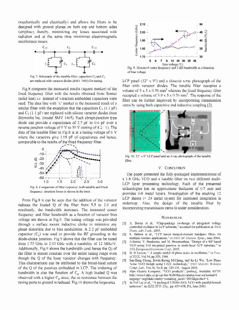
From Fig.8 it can be seen that the addition of the varactorreduces the loaded Q of the filter from 5.5 to 2.6 andresultantly, the bandwidth increases. The measured centerfrequency and filter bandwidth as a function of varactor biasvoltage are shown in Fig.9. The tuning voltage was providedthrough a surface mount inductive choke to minimize any
phase distortion due to bias modulation. A 2.2 pF embeddedcapacitor (Cg) was used to provide the RF grounding at thediode-choke junction. Fig.9 shows that the filter can be tunedfrom 1.75 GHz to 2.03 GHz with a tunability of 12 MHz/V.Additionally, Fig.9 shows the bandwidth (and hence the Q) ofthe filter is almost constant over the entire tuning range even
though the Q of the lossy varactor changes with frequency.This characteristic can be attributed to the broad-band natureof the Q of the passives embedded in LCP. The widening ofbandwidth is also the function of Cg. A high loaded Q was
observed with a higher Cg since, the ac resistance between thetuning ports to ground is reduced. Fig. 10 shows the large-area
2.10N
- 2.00 -
0
= 1.90-
Q 1.80-
1.70
50
45 9;
-40 C
-35 i
305 6 7 8 10 15 20 25 28
Bias voltage (V)Fig. 9. Measured center frequency and 3 dB bandwidth as a functionof bias voltage
LCP panel (12" x 9") and a close-in x-ray photograph of thefilter with varactor diodes. The tunable filter occupies avolume of 5 x 5 x 0.76 mm3 whereas the fixed frequency filteroccupied a volume of 3.9 x 5 x 0.76 mm3. The response of thefilter can be further improved by incorporating transmissionzeros by using both capacitive and inductive coupling [2].
Fig. 10. 12" x 9" LCP panel and an X-ray photograph ofthe tunablefilter.
V. CONCLUSION
The paper presented the fully-packaged implementations ofa 1.8 GHz VCO and a tunable filter on two different multi-LCP layer processing technology. Each of the presentedtechnologies has an approximate thickness of 0.7 mm andprovides 6-8 metal layers. Investigation of the stacking 12LCP sheets (> 24 metal layers) for increased integration isunderway. Also, the design of the tunable filter byincorporating transmission zeros is under consideration.
REFERENCES[1] A. Bavisi et al., "Chip-package co-design of integrated voltage
controlled oscillator in LCP substrate," accepted for publication at IEEETrans. Adv. Pack., 2005.
[2] S. Dalmia et al., "LCP based lumped-element bandpass filters formultiple wireless applications," in IEEE Int. Microw. Symp., June 2004.
[3] A.Bavisi, V. Sundaram, and M. Swaminathan, "Design of a SiP basedVCO using 3-D integrated passives in multi-layer LCP substrate," in35th European Microwave Conf, 2005.
[4] D. B Leeson, " A simple model of phase noise in oscillators," in Proc.ofIEEE, Vol.54, pp.329, 1966
[5] Sin-Hang Cheng, Kwok-Kueng M.Cheng, and Ke-Li Wu, "Low PhaseNoise VCO Design using LTCC technology," IEEE Microw. WirelessComp. Lett., Vol.30, No.8, pp. 329-33 1, August 2003.
[6] Alps Electric Company, "VCO products", [online], Available HTTP:http://www3.alps.co.jp/cgi-bin/WebObjects/catalog.woa/wa/normal?language=english&country=com&top_mode=2003&product=I.
[7] Ja-Yol Lee et al., "A packaged 2.3GHz SiGe VCO with parallel-branchinductors", in IEEE RFIC Dig., pp. 655-658, PA, June 2003.